1
No. CP-SP-1096E
SDU10
Compact Operation Unit
for the DMC10 Distributed Multi-channel Controller
User's Manual
Thank you for purchasing the SDU10 Compact
Operation Unit for the DMC10 Distributed Multi-channel
Controller .
This manual contains information for ensuring correct
use of the SDU10. It also provides necessary information for installation, maintenance, and troubleshooting.
This manual should be read by those who design and
maintain devices that use the SDU10.
Be sure to keep this manual nearby for handy reference.
Contents
1. INTRODUCTION & SYSTEM CONFIGURATION ...1
2. NAMES & FUNCTIONS OF PARTS ........................2
3. MOUNTING..............................................................2
4. WIRING....................................................................4
5. OPERATION PROCEDURES..................................7
6. RECIPE FUNCTION ..............................................23
7. HOST COMMUNICATIONS FUNCTION ...............24
8. ALARM CODES ....................................................25
9. SPECIFICATIONS .................................................26
Appendix 1. USER-DEFINED ITEM NAMES............27
Appendix 2. USE OF AN SDU10 AS A SLAVE........28
Appendix 3. SDU10 INTERNAL SETUP DATA
BATCH COPY FUNCTION ...................29
Appendix 4. SDU10 COMMUNICATIONS
PARAMETER TABLES.........................31
RESTRICTIONS ON USE
This product has been designed, developed and manufactured for general-purpose
application in machinery and equipment.
Accordingly, when used in applications outlined below, special care should be taken to
implement a fail-safe and/or redundant design concept as well as a periodic
maintenance program.
• Safety devices for plant worker protection
• Start/stop control devices for transportation and material handling machines
• Aeronautical/aerospace machines
• Control devices for nuclear reactors
Never use this product in applications where human safety may be put at risk.
NOTICE
Be sure that the user receives this manual before the product is used.
Copying or duplicating this user’s manual in part or in whole is forbidden. The information and specifications in this manual are subject to
change without notice.
Considerable effort has been made to ensure that this manual is free
from inaccuracies and omissions. If you should find an error or omission, please contact Yamatake Corporation.
In no event is Yamatake Corporation liable to anyone for any indirect,
special or consequential damages as a result of using this product.
©2000 Yamatake Corporation ALL RIGHTS RESERVED
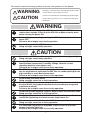
This manual uses the following symbols to ensure safe operation of this device.
WARNING
CAUTION
Warnings are indicated when mishandling this product might
result in death or serious injury to the user.
Cautions are indicated when mishandling this product might
result in minor injury to the user, or only physical damage to
this product.
WARNING
Note that incorrect wiring of the SDU10 can damage the SDU10 and
lead to other hazards. Check that the SDU10 has been correctly wired
before turning the power ON.
Before wiring, or removing/mounting the SDU10, be sure to turn the
power OFF.
Failure to do so might cause faulty operation.
Do not disassemble the SDU10.
Doing so might cause faulty operation.
CAUTION
Do not operate the keys with a propelling pencil or sharp-tipped object.
Doing so might cause faulty operation.
Use the SDU10 within the operating ranges recommended in the
specifications (temperature, humidity, voltage, vibration, shock,
mounting direction, atmosphere, etc.).
Failure to do so might cause fire or faulty operation.
The SDU10 used with the rubber packing enclosed in the package satisfies the requirements equivalent to IP65. Use the rubber packing for the
high humidity or much dust environment.
Failure to do so might cause fire or faulty operation.
Do not block ventilation holes.
Doing so might cause fire or faulty operation.
Wire the SDU10 properly according to predetermined standards. Also
wire the SDU10 using specified power leads according to recognized
installation methods.
Failure to do so might cause fire or faulty operation.
Do not allow leads clippings, chips or water to enter the controller case.
Doing so might cause fire or faulty operation.
Firmly tighten the terminal screws at the torque listed in the specifications.
Insufficient tightening of terminal screws might cause fire.
Do not use unused terminals on the SDU10 as relay terminals.
Doing so might cause fire or faulty operation.
Use Yamatake Corporation’s SurgeNon if there is the risk of power
surges caused by lightning.
Failure to do so might cause fire or faulty operation.
i
Unpacking
Check the following items when removing the SDU10 from its package:
Name
Model No.
Q’ty
Body
SDU10T0100
1
Mounting bracket
User’s Manual
Unit indicator seal
Rubber packing
81446403-001
CP-SP-1096E
1
1
1
1
Remarks
This manual
After unpacking, handle the SDU10 and its accessories taking care to prevent damage or loss of parts.
If an inconsistency is found or the package contents are not in order, immediately contact your dealer.
Conventions Used in This Manual
The following conventions are used in this manual:
Handling Precautions
: Handling Precautions indicate items that the user should pay attention to
when handling the SDU10.
Note
: Notes indicate useful information that the user might benefit by knowing.
ii
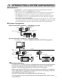
1. INTRODUCTION & SYSTEM CONFIGURATION
■ Introduction
The SDU10 is a compact operation display unit for the Modular Controller
DMC10. The features of the SDU10 are as follows:
• The compact size of the SDU10 enables it to be installed in restricted spaces.
• Only the necessary number of locations can be monitored and operated.
• The SDU10 can be used as a monitor/operation device especially for on-site
use in addition to use as a communications device with a personal computer,
touch panel or other host device.
• The recipe function enables DMC10 setup parameters (SP, P, I, D, etc.) that differ
according to product lot to be stored internally on the SDU10 so that they can be
batch changed by key operation, external switch input and communications.
■ System Configuration
● Instrumentation example 1: Host device no exist
Slave (See Appendix 2.)
Master
SDU10
SDU10
Slave communications
Slave communications
DMC10 max. 15 units
RS-485
4
ADR 0
4
LDR
ADR 0
8
C
CH3
PWR
23
21
22
22
23
23
24
24
24
25
DMC10
21
17
22
18
23
19
24
20
25
21
21
22
22
23
23
24
24
25
25
DMC10
DMC10
25
4
LDR
ADR 0
8
PWR
17
18
19
20
23
24
25
DMC10
21
22
23
24
25
CH1
16
17
23
18
18
24
19
25
PWR
22
17
24
LDR
21
16
23
8
C
CH3
CH1
22
19
25
20
CH4
22
ADR 0
PWR
21
CH2
21
4
LDR
8
C
CH3
CH1
16
CH4
25
24
25
25
16
CH2
21
23
23
24
25
CH4
C
CH3
CH1
24
20
22
22
4
ADR 0
PWR
23
19
CH2
21
21
22
LDR
8
C
CH3
22
18
CH4
CH2
21
4
ADR 0
21
17
25
20
CH4
16
24
19
25
CH1
23
18
24
PWR
22
17
23
LDR
21
16
22
8
C
CH3
CH1
21
20
CH4
CH2
21
21
22
22
23
23
24
24
25
25
DMC10
CH2
21
22
23
24
25
DMC10
● Instrumentation example 2: Host device exist
For details, see “7. HOST COMMUNICATIONS FUNCTION” (page 24).
Host device
RS-485
Host
communications
Master
Host
communications
Slave (See Appendix 2.)
SDU10
SDU10
Slave
communications
SDU10
Slave communications
Slave communications
DMC10 max. 15 units
4
ADR 0
RS-485
4
LDR
ADR 0
8
C
CH3
PWR
16
22
17
23
18
24
19
25
20
CH4
21
22
23
24
25
17
23
18
24
24
19
25
25
23
24
25
DMC10
23
24
25
16
20
CH4
CH2
21
21
22
22
23
23
24
24
25
25
DMC10
ADR 0
PWR
17
22
18
23
19
24
20
25
16
17
18
19
20
CH4
21
21
22
22
23
23
24
24
25
25
22
17
23
18
24
19
25
20
23
24
25
DMC10
21
22
23
24
25
22
17
23
18
24
19
25
20
22
23
24
25
DMC10
21
22
23
24
25
22
17
23
18
24
19
25
20
23
24
25
DMC10
21
22
23
24
25
23
18
24
24
19
25
25
20
23
24
25
DMC10
23
24
25
CH4
CH2
21
21
22
22
23
23
24
16
21
17
22
18
23
19
24
20
25
CH2
21
22
22
23
23
24
24
25
25
25
DMC10
DMC10
24
25
ADR 0
PWR
17
18
19
20
16
17
23
18
24
19
25
20
23
24
25
DMC10
21
22
23
24
25
23
24
25
DMC10
CH1
16
22
17
23
18
24
19
25
20
CH4
22
PWR
21
CH2
21
LDR
8
C
CH3
CH1
22
CH4
22
ADR 0
PWR
21
CH2
21
4
LDR
8
C
CH3
CH1
16
CH4
21
4
LDR
8
C
CH3
CH1
22
17
23
22
4
ADR 0
PWR
21
22
21
LDR
8
C
CH3
CH1
16
CH4
22
ADR 0
PWR
21
CH2
21
4
LDR
8
C
CH3
CH1
16
CH4
22
ADR 0
PWR
21
CH2
21
4
LDR
8
C
CH3
CH1
16
CH4
21
4
ADR 0
PWR
21
CH2
DMC10 max. 15 units
RS-485
LDR
8
C
CH3
CH1
16
CH4
22
ADR 0
PWR
21
CH2
21
4
LDR
8
C
CH3
CH1
21
CH2
DMC10
4
LDR
8
C
CH3
CH1
22
23
22
4
ADR 0
PWR
21
22
21
LDR
8
C
CH3
CH1
16
CH4
22
ADR 0
PWR
21
CH2
21
4
LDR
8
C
CH3
CH1
21
Master
21
22
23
24
25
CH2
21
22
23
24
25
DMC10
Handling Precautions
• The RS-232C⇔RS-485 converter is needed when performing communications
with the host device (including the EST240Z touch panel) on the RS-232C
interface. The Yamatake Corporation CMC10L can also be used.
• When accessing the DMC10 from the host device via the SDU10, set the timeout for when there is no response to at least one second. Accessing of SDU10
data is determined by SDU10 setup C04.
• The SDU10 cannot be used together with the CMC10A or B.
• The host device cannot communicate with the Yamatake's SDC series (slave)
via the SDU10.
1
2. NAMES & FUNCTIONS OF PARTS
PV, SP lamps:
Indicate the content displayed on the upper and
lower displays.
• Only PV lamp lit:
PV value on both upper and lower displays
• Only SP lamp lit:
SP value on both upper and lower displays
• Both PV and SP lamp lit:
PV value on upper display and SP on lower
display
Moves between DMC10 channels.
RDY
key:
Hold down for at least 1s to activate preset
functions. Factory setting is disabled.
Common mode lamps:
F1: Lit/blinks when function preset to F1 is ON.
F2: Lit/blinks when function preset to F2 is ON.
F3: Lit/blinks when function preset to F3 is ON.
F4: Lit/blinks when function preset to F4 is ON.
AL1: Blinks when an SDU10 communications error
occurs. Lights when an SDU10 memory error
occurs.
AL2: Blinks when a DMC10 PV error occurs. Lights
when a DMC10 memory error occurs.
F1
RDY
CH
SP
F2
F3
F4 AL1 AL2
CH
Upper display: Displays PV values or setup items.
Channel display:
Displays the channel No. on
the DMC10.
PARA
key:
PV
No
Address display:
Displays the device address
No. of the DMC10 unit.
CH
MAN
AT
RDY
MAN
AT
RDY
CH
key:
PARA
SDU10
Switches the display items.
Hold down for at least 3s or 6s depending on the
display item.
Upper mode lamps:
Indicate the states of channels in the upper display.
MAN: Lights in the Manual mode.
AT: Lights in the Auto-tuning mode or Self-tuning
mode.
RDY: Lights when ready.
Lower display: Displays PV values or setup items
Lower mode lamps:
Indicate the states of channels in the lower display.
MAN: Lights in the Manual mode.
AT: Lights in Auto-tuning mode or Self-tuning
mode.
RDY: Lights when ready.
key:
Used for incrementing numeric values and performing
arithmetic shift operations.
3. MOUNTING
■ External Dimensions
Unit: mm
* Dimension becomes 3mm when the unit is used with the
rubber packing.
2*
48
38
44.8
PV
No
CH
SP
F1
F2
F3
RDY
F4 AL1 AL2
CH
MAN
AT
MAN
AT
44.8
48
CH
RDY
RDY
PARA
SDU10
■ Panel Cutout
(48 X N -3) +0.5
0
2
45+0.5
0
45+0.5
0
45 +0.5
0
Unit: mm
■ Mounting Locations
Do not install the SDU10 in locations where it is:
• subject to extreme temperature and humidity
• subject to sulfuric or corrosive gases
• subject to dust or oil smoke
• subject to direct sunlight, or splashing by rain or water
• subject to mechanical vibrations and shock
• subject to high-voltage lines, welding machines and sources of electric noise
• less than 15m from high-voltage ignition devices
• subject to electromagnetic fields
• subject to flammable liquids or vapor
Handling Precautions
The inside of the SDU10 cannot be drawn out of its case.
■ Mounting Method
CAUTION
Use the SDU10 within the operating ranges recommended in the specifications (temperature, humidity, voltage, vibration, shock, mounting direction,
atmosphere, etc.).
Failure to do so might cause fire or faulty operation.
The SDU10 used with the rubber packing enclosed in the package satisfies
the requirements equivalent to IP65. Use the rubber packing for the high
humidity or much dust environment.
Failure to do so might cause fire or faulty operation.
Do not block ventilation holes.
Doing so might cause fire or faulty operation.
● Required tools
Phillips screwdriver for
turning M2.5 screws
● Procedure
(1)Insert the SDU10 into the
opening on the front side
of the panel.
Panel
Mounting bracket
(2)Attach the mounting bracket at the rear side of the panel.
(3)Press the SDU10 against the mounting bracket to make sure that the bracket
claws enter the grooves of the controller.
(4)Tighten the top and bottom screws. (When the screws touch the panel, turn the
screws another half turn.)
Handling Precautions
• Do not operate the keys with a propelling pencil or sharp tipped
object. Be sure to mount this SDU10 on a panel.
• Do not overtighten the screws to prevent deformation of the front
panel.
3
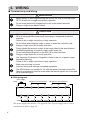
4. WIRING
■ Terminal Array and Wiring
WARNING
Before wiring, or removing/mounting the SDU10, be sure to turn the power
OFF. Failure to do so might cause faulty operation.
Do not touch electrically charged parts such as the power terminals.
Doing so might cause electric shock.
CAUTION
Wire the SDU10 properly according to predetermined standards. Also wire the
SDU10 using specified power leads according to recognized installation
methods.
Failure to do so might cause fire or faulty operation.
Do not allow leads clippings, chips or water to enter the controller case.
Doing so might cause fire or faulty operation.
Firmly tighten the terminal screws at the torque listed in the specifications.
Insufficient tightening of terminal screws might cause fire.
Do not use unused terminals on the SDU10 as relay terminals.
Doing so might cause fire or faulty operation.
Use Yamatake Corporation’s SurgeNon if there is the risk of power surges
caused by lightning.
Failure to do so might cause fire or faulty operation.
Make sure all wiring is correct.
Incorrect wiring may damage connected equipment.
The SDU10 does not operate for 15s after the power has been turned ON.
Special arrangements must be made when the device signals are to be used
as an interlock signal.
● Wiring diagrams
Power supply*
RS-485 host communications
24Vdc
+
–
2
1
9
10
EV2
EV1
RSW8
RSW7
RS-485 slave communications
DA
DB
SG
DA
DB
SG
3
4
5
6
7
8
11
RSW6
12
RSW5
13
RSW4
14
RSW3
15
RSW2
16
RSW1
*The power supply unit must be a UL approved Class 2 power supply unit or Class 2
transformer in order to apply UL.
4
Handling Precautions
• Check the model number of the display unit and terminal numbers on the label
on the side of the display unit to prevent any wiring errors.
• When wiring, take care to prevent leads from contacting adjacent terminals.
• Do not use unused terminals as relay terminals.
• Two or more SDU10 display units can be connected in parallel by external
switch input.
• The display unit can be connected with the Yamatake Corporation
SDC10/20/30/40 series in parallel by external switch input.
• Before connecting in parallel to other equipment, first check the conditions of
the other equipment.
• A common terminals is used for external switch input (RSW7, 8) and event output (EV1, 2). To use only external switch input, do not set event output.
Alternately, do not set external switch input when only event output is to be
used. The following figure shows the circuit configuration of this terminal:
For event output
+
Load
9 or 10
●
(To RSW circuit)
●
From EV circuit
−
8
●
●
For external switch input
Contact
9 or 10
●
To RSW circuit
●
(From EV circuit)
8
●
●
• A mechanism, which does similar function to the terminating resistor, is builtinto the host communications and slave communications of the SDU10.
Therefore, do not connect any external terminating resistor to the SDU10.
(For details, see the next page.)
Even though a device instructed to connect a terminating resistor is connected
to the same line, to which the SDU10 is connected, do not connect any terminating resistor. Doing so might cause a communication error to occur.
● Cable specifications
• Wire type: Single wire and strand wire both acceptable
• Wire size: 0.13 to 1.31mm2 (AWG26 to 16)
• Recommended stripped length : 4mm
4mm
5
■ Meaning of Symbols in the Terminal Wiring Label
The following table shows the meanings of symbols in the terminal wiring label
on the side of the instrument:
Symbol
Description
Direct current
CAUTION
Note
Terminating resistor
Basically, the terminating resistor provides two main aims.
One is that the matching with the cable impedance is made to suppress the reflection of the communication signal.
The other is that the impedance is decreased by the terminating resistor to make
the communications stable.
Generally, the former is effective when the transmission speed is high (at a speed
of several Mbps). According to Yamatake's past results, even if the terminating
resistor is connected or not, the communication waveform is not disturbed even
though the cable is run up to 500 m.
(Even though the waveform is actually observed, almost no changes are found.)
For the latter, there is a method that the impedance of a communication line is
decreased inside the product even without use of a terminating resistor.
This unit uses such method.
Therefore, if any external terminating resistor is connected to this unit, it may
conflict with the internal circuit, causing the communications not to be established.
In this case, however, even though any conflict occurs, this does not cause any
damage to the product.
The communications system of Yamatake's products (DMC10, SDU10, and
CMC10G) is designed like the foregoing.
Even though other company's product recommends to connect a terminating resistor when performing the communications with Yamatake's product connected to
other company's product, the terminating resistor must not be connected to
Yamatake's product since its internal circuit provides similar effect.
Additionally, as a background, in which the above method is used, this method
ensures the energy saving of the customer's equipment.
6
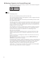
5. OPERATION PROCEDURES
Complete the setup for slave DMC10s before setting up the SDU10.
Step
1
See Page
10
Set SDU10 setup items.
Make the initial settings on the SDU10 itself.
Step
2
Execute C27 (execute automatic detection).
Step
3
Set recipe items.
16
19
Set the recipe items only when the recipe functions are used. For details, see “6. RECIPE FUNCTION.”
Step
4
Read DMC10 parameters for recipes.
19
Perform this operation only when the recipe functions are used.
Handling Precautions
After setting up the DMC10s, Execute the function prompt "execute automatic
detection (C27)".
If not, the settings in the DMC10s are not reflected to the operation of the
SDU10.
How to Set up Data
Procedure
(1)Enter numeric values with the
keys.
No
CH
MAN
AT
RDY
MAN
AT
RDY
CH
PARA
(Note)
“
” is displayed in the
lower display for about 2s
to indicate that an incorrect
key or data entry was made.
Such entries are ignored.
No
CH
Numeric values blink for
about 2s.
During blinking, the PARA
key cannot be used.
Blinking stops to indicate
that the data has been set.
No
MAN
AT
RDY
MAN
AT
RDY
CH
CH
PARA
MAN
AT
RDY
MAN
AT
RDY
CH
PARA
7
■ Overall Operation Flow
Power ON
PV
No
F1
RDY
CH
SP
F2
F3
F4 AL1 AL2
CH
This value is displayed for 15s.
MAN
AT
MAN
AT
RDY
CH
RDY
PARA
SDU10
Press the
Press the
Previous display channel monitor
• PV/SP (PV/PV) monitor
(• SP/SP monitor)
(• CT monitor)
(• Max./min. PV monitor)
(• SP set selection screen)
(• Recipe set selection screen)
Hold down the
PARA key for 3s.
key.
Press the
Next channel monitor
CH
CH
• PV/SP (PV/PV) monitor
(• SP/SP monitor)
(• CT monitor)
(• Max./min. PV monitor)
(• SP set selection screen)
(• Recipe set selection screen)
• PV/SP (PV/PV) monitor
(• SP/SP monitor)
(• CT monitor)
(• Max./min. PV monitor)
(• SP set selection screen)
(• Recipe set selection screen)
Hold down the
PARA key for 3s.
CH
Hold down
the PARA key
for 6s.
(• CF20: User-defined setting 20)
CH
key.
Press the
Change setting of above channel.
• SP (SP1): SP value (SP1 value)
(• SP2: SP2 value)
(• SP3: SP3 value)
(• SP4: SP4 value)
(• SP5: SP5 value)
(• SP6: SP6 value)
(• SP7: SP7 value)
(• SP8: SP8 value)
• SPA:SP set in use
• AT: Start Auto-tuning
• P: Proportional band
• I: Reset time
• D: Rate time
• PbIA: PV vias
(• CF1: User-defined setting 1)
CH
(• CF20: User-defined setting 20)
SDU10 setup
8
PARA
key for 3s.
Hold down the
Recipe items
CH
key.
Change setting of above channel.
• SP (SP1): SP value (SP1 value)
(• SP2: SP2 value)
(• SP3: SP3 value)
(• SP4: SP4 value)
(• SP5: SP5 value)
(• SP6: SP6 value)
(• SP7: SP7 value)
(• SP8: SP8 value)
• SPA:SP set in use
• AT: Start Auto-tuning
• P: Proportional band
• I: Reset time
• D: Rate time
• PbIA: PV vias
(• CF1: User-defined setting 1)
key.
DMC10
setting
change
(• CF20: User-defined setting 20)
Hold down the
Hold down the
DMC10
monitor
Hold down the
PARA key for 3s.
Press the
Press the
Change setting of above channel.
• SP (SP1): SP value (SP1 value)
(• SP2: SP2 value)
(• SP3: SP3 value)
(• SP4: SP4 value)
(• SP5: SP5 value)
(• SP6: SP6 value)
(• SP7: SP7 value)
(• SP8: SP8 value)
• SPA:SP set in use
• AT: Start Auto-tuning
• P: Proportional band
• I: Reset time
• D: Rate time
• PbIA: PV vias
(• CF1: User-defined setting 1)
key.
key.
Nth unit M channel monitor
PARA
PARA
key for 3s.
key for 3s.
Read to recipe set
• C01: Key lock
• C02: Slave device setting
• C03: Device address
• C04: Host communications conditions
• C05: Slave communications conditions
• C06: Display method in Run mode
• C07: LED operation type
• C08: RDY key function
• C09: Event 1 operation type
• C10: Event 2 operation type
• C11: External switch input 1 operation type
(• r1: Recipe item 1)
(• r2: Recipe item 2)
(• r3: Recipe item 3)
(• r4: Recipe item 4)
(• r5: Recipe item 5)
(• r6: Recipe item 6)
(• r7: Recipe item 7)
(• r8: Recipe item 8)
(• r9: Recipe item 9)
(• r10: Recipe item 10)
(• r11: Recipe item 11)
(• rf1: Recipe set 1)
(• rf2: Recipe set 2)
(• rf3: Recipe set 3)
(• rf4: Recipe set 4)
(• rf5: Recipe set 5)
(• rf6: Recipe set 6)
(• rf7: Recipe set 7)
(• rf8: Recipe set 8)
(• rf9: Recipe set 9)
(• rf10: Recipe set 10)
(• rf11: Recipe set 11)
(• C112: Event 2 onderey)
(• r199: Recipe item 199)
(• rf99: Recipe set 99)
SDU10
settings
Note
• The “previous displayed channel” refers to the device address and channel of the
DMC10 that was last monitored, and monitoring starts from that address and channel.
The
hatched section are sometimes not displayed depending on the SDU10 setup
details. The next parameter is moved to within each group by pressing the PARA key as
normal.
• For details of actual displays, refer to ■ DMC10 Monitoring (page 19).
• The display transition when the
as follows:
CH
key is pressed on the DMC10 monitor screen is
Press the CH key
Press the CH key
Press the CH key
Press the CH key
Press the CH key
Press the CH key
Press the CH key
Press the CH key
9
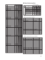
■ List of SDU10 Setup Items
M: Setting enabled when in the Master mode
M, S: Setting enabled when in either the Master or Slave mode
*1: For the parameters of which each digit has its own setting content individually,
the rightmost digit is the first digit.
*2: Use DMC10 version 7.XX onwards.
Function
Item
Prompt
C01
Key lock
10
C02
Slave device setting
C03
C04
Device address
Host communications
settings *1
C05
Slave communications
settings *1
C06
Display method in Run
mode *1
Description
Factory Master /
Setting Slave
0 M, S
0 : Key lock not engaged
1 : All setup items excluding key lock cannot be set
2 : Only key lock and SP set/recipe set switching are available
3 : All parameters excluding key lock cannot be set
0 : Master
0
1 : Slave
0 to 127 : Address conversion OFF
0
1st digit: Transmission speed
0002
0 : 4800bps
1 : 9600bps
2 : 19200bps
2nd digit: Communication format
0 : 8bits, even parity, 1 stop bit
1 : 8bits, no parity, 2 stop bits
2 : 7bits, even parity, 1 stop bit
3 : 7bits, no parity, 2 stop bits
3rd digit: Min. communications response time
0 : 1ms
1 : 10ms
2 : 100ms
3 : 200ms
4th digit: Communications protocol
0 : CPL
1 : MOD BUS (ASCII)
2 : MOD BUS (binary)
1st digit: Transmission speed
0002
0 : 4800bps
1 : 9600bps
2 : 19200bps
2nd digit: Communication format
0 : 8bits, even parity, 1 stop bit
1 : 8bits, no parity, 2 stop bits
2 : 7bits, even parity, 1 stop bit
3 : 7bits, no parity, 2 stop bits
3rd digit: Communications time-out
0 : 500ms
1 : 1000ms
2 : 2000ms
4th digit:
0 : Fixed
1st digit: Basic display (upper/lower)
0000
0 : PV/SP display
1 : PV/PV display
2 : PV/PV display + SP/SP display
3 : PV/SP display + CT display
4 : PV/PV display + CT display
5 : PV/PV display + SP/SP display + CT display
2nd digit: Min./max. CT/PV value display
0 : Does not display
1 : Min./Max. PV value display
2 : Min./Max. PV value display (peak hold)
3rd digit: SP set change/recipe set change screen display
0 : Does not display
1 : SP set selection screen only
2 : Recipe set selection screen only
3 : SP set selection screen + recipe set selection screen
4th digit: Fixed/scan display mode selection
0 : Fixed display
1 : Scan display
M, S
M, S
M, S
M, S
M
Function
Item
Prompt
C07
LED operation type
C08
RDY key function *1
C09
C10
Event 1 operation type *1
Event 2 operation type *1
C11
C12
C13
C14
C15
C16
C17
C18
C19
C20
External switch input 1 operation type
External switch input 2 operation type
External switch input 3 operation type
External switch input 4 operation type
External switch input 5 operation type
External switch input 6 operation type
External switch input 7 operation type
External switch input 8 operation type
C21
C22
C23
C27
C28
C29
Description
F1
F2
F3
F4
0 : None
EV2
EV3
EV4
1 : DMC10 event output state: EV1
EV bus 1 EV bus 2 EV bus 3 EV bus 4
2 : DMC10 bus output state:
Communi- Communi- Communi- Communi3 : DMC10 communications
cations DI1 cations DI2 cations DI3 cations DI4
DI input state *2:
4 : DMC10 external switch input state RSW1 RSW2 RSW3 RSW4
5 : DMC10 control output state: OUT1 OUT2 OUT3 OUT4
6 : DMC10 selected SP set display:
(MSB) binary display (LSB)
7 : SDU10 selected recipe set:
8 : SDU10 communications state: Up TXD Up RXD Down TXD Down RXD
1st digit: RDY key function
0 : None
1 : RUN/READY *2 (all modules, all channels)
2 : RUN/READY (indicated module, upper display channel)
3 : Auto-tuning *2 (all modules, all channels)
4 : Auto-tuning (indicated module, upper display channel)
5 : SP set switching *2
6 : Recipe set switching
7 : SDU10 event latch canceled
2nd digit
0 : Fixed
3rd digit: SP set/recipe switching by RDY key
0 : Switching of 2 sets
1 : Switching of 3 sets
2 : Switching of 4 sets
4th digit
0 : Fixed
1st digit
0 : None
1 : ON output when error lamp lights
2 : ON output when desired channel is ready
3 : ON output when auto-tuning is executed on desired channel
4 : ON output when event 5 of all modules is ON
5 : ON output when event tables 5 to 8 of all modules are ON
6 : ON output when event table 5 of a desired module is ON
7 : ON output when event tables 5 to 8 of a desired module are ON
8 : Upper/lower limits of Min./Max. PV value
2nd digit
0 : Direct
1 : Reverse
3rd digit
0 : Latch disabled
1 : Latch enabled
4th digit
0 : Fixed
0 : None
1 : RUN/READY *2 (all channels)
2 : Auto-tuning start/stop *2 (all channels)
3 : SP set switching
4 : Recipe switching
5 : Event latch release
6 : Clearing the Min./Max. PV value
Number of user-defined items Adds the number of items to DMC10 Setup screen. (0 to 20)
Number of additional buffers Determines the number of configurations used in buffered
communications. (0 to 10)
Number of recipe items Sets the number of items per recipe. (0 to 199)
Number of recipe sets
Sets the number of recipe sets. (0 to 99)
DMC10 setup screen
Bit 0 : SP (0 : display, 1 : hide)
display settings
Bit 1 : AT (0 : display, 1 : hide)
Bit 2 : P (0 : display, 1 : hide)
Bit 3 : I (0 : display, 1 : hide)
Bit 4 : D (0 : display, 1 : hide)
Bit 5 : PbIA (0 : display, 1 : hide)
Bit 6 to 15 : Unused
Execute automatic detection 0 : End automatic detection
1 : Execute automatic detection
Automatic detection results Number of automatically detected DMC10
Version information
Current version
Factory Master /
Setting Slave
0
M
0000
M
0000
M, S
0
M, S
0
0
M
M
0
0
M
M
0
M
0
M
0
–
M
M, S
11
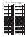
Function
Prompt
C30
C31
C32
C33
C34
C35
C36
C37
C38
C39
C40
C41
C42
C43
C44
C45
C46
C47
C48
C49
C50
C51
C52
C53
C54
C55
C56
C57
C58
C59
C60
C61
C62
C63
C64
C65
C66
C67
C68
C69
C70
C71
C72
C73
C74
C75
C76
C77
C78
C79
C80
C81
C82
C83
C84
C85
C86
C87
C88
C89
12
Item
User-defined item 1 address
User-defined item 2 address
User-defined item 3 address
User-defined item 4 address
User-defined item 5 address
User-defined item 6 address
User-defined item 7 address
User-defined item 8 address
User-defined item 9 address
User-defined item 10 address
User-defined item 11 address
User-defined item 12 address
User-defined item 13 address
User-defined item 14 address
User-defined item 15 address
User-defined item 16 address
User-defined item 17 address
User-defined item 18 address
User-defined item 19 address
User-defined item 20 address
User-defined item 1 name
User-defined item 2 name
User-defined item 3 name
User-defined item 4 name
User-defined item 5 name
User-defined item 6 name
User-defined item 7 name
User-defined item 8 name
User-defined item 9 name
User-defined item 10 name
User-defined item 11 name
User-defined item 12 name
User-defined item 13 name
User-defined item 14 name
User-defined item 15 name
User-defined item 16 name
User-defined item 17 name
User-defined item 18 name
User-defined item 19 name
User-defined item 20 name
User-defined item 1 decimal point
User-defined item 2 decimal point
User-defined item 3 decimal point
User-defined item 4 decimal point
User-defined item 5 decimal point
User-defined item 6 decimal point
User-defined item 7 decimal point
User-defined item 8 decimal point
User-defined item 9 decimal point
User-defined item 10 decimal point
User-defined item 11 decimal point
User-defined item 12 decimal point
User-defined item 13 decimal point
User-defined item 14 decimal point
User-defined item 15 decimal point
User-defined item 16 decimal point
User-defined item 17 decimal point
User-defined item 18 decimal point
User-defined item 19 decimal point
User-defined item 20 decimal point
Description
256 to 9999:Set the address of items to be added in the
DMC10 Setup screen.
Can be entered using the characters in Appendix 1.
0 : No decimal point
1 : Decimal point No.1
2 : Decimal point No.2
3 : Decimal point No.3
Factory Master /
Setting Slave
256
M
CF 1
CF 2
CF 3
CF 4
CF 5
CF 6
CF 7
CF 8
CF 9
CF 10
CF 11
CF 12
CF 13
CF 14
CF 15
CF 16
CF 17
CF 18
CF 19
CF 20
0
M
M
M
M
M
M
M
M
M
M
M
M
M
M
M
M
M
M
M
M
M
Function
Prompt
C90
C91
C92
C93
C94
C95
C96
C97
C98
C99
C101
C102
C103
C104
C105
C106
C107
C108
C109
C110
C111
C112
Factory Master /
Setting Slave
Additional buffering address 1 256 to 9999:Sets the address of items to be additionally buffered.
256
M
Additional buffering address 2
Additional buffering address 3
Additional buffering address 4
Additional buffering address 5
Additional buffering address 6
Additional buffering address 7
Additional buffering address 8
Additional buffering address 9
Additional buffering address 10
Event 1 setting value A -1999 to +9999
0 M, S
Event 1 setting value B -1999 to +9999
0 M, S
Position of decimal point 0 to 3
0 M, S
in event 1 setting value A
Position of decimal point 0 to 3
0 M, S
in event 1 setting value B
Event 1 standby
0 : Non
0 M, S
1 : Standby
Event 1 ON delay
0 to 9999(s)
0 M, S
Event 2 setting value A -1999 to +9999
0 M, S
Event 2 setting value B -1999 to +9999
0 M, S
Position of decimal point 0 to 3
0 M, S
in event 2 setting value A
Position of decimal point 0 to 3
0 M, S
in event 2 setting value B
Event 2 standby
0 : Non
0 M, S
1 : Standby
Event 2 ON delay
0 to 9999(s)
0 M, S
Item
Description
13
■ Item Descriptions
● C01 (key lock)
The relationship between the value set in this parameter and the parameters which
can be set with the value. Key lock can be set in any case.
«:Available
Setting Setup
DMC10 setting SP set / Recipe set
parameter
parameter
change parameter
✕ :Not available
0
1
2
3
«
✕
✕
✕
«
«
✕
✕
«
«
«
✕
● C02 (slave device setting)
This item enables the display of data in the master device on a specified slave
device. This item is mainly used for monitoring all PV values simultaneously on a
4-channel model. PV values are only displayed on the slave device, and key operations are disabled except for setup items.
● C03 (device address)
This item need not be set when host communications is not performed.
For details, see “7. HOST COMMUNICATIONS FUNCTION” (page 19).
When adding an SDU10 to instrumentation that was communicating directly
with a DMC10, set this item to “0”.
The device address must be specified, for example, when there are 16 or more
DMC10s.
When MODBUS is set for the host communication conditions, the host communications cannot be performed for the 16 to 127 setting.
● C06 (display method in Run mode)
“Min./max. value display” refers to display of the minimum value (lower display)
and maximum value (upper display) of all PV values of all DMC10s currently
connected to the SDU10.
“Scan display” is a function for automatically switching and displaying channels
at 4-second intervals. The values of all channels can be monitored even from a
remote locations as key operation is not required.
● C07 (LED operation type)
This item is for setting the operation conditions for LEDs F1 to F4 on the front
panel.
For setting “3: DMC10 communications DI input state,” use DMC10 version
7.XX onwards.
● C08 (RDY key function)
1st digit
1: RUN/READY (all modules, all channels):
RUN/READY operation is executed on all channels based upon the
RUN/READY state of the channel currently displayed on the upper display.
Use DMC10 version 7.XX onwards.
14
1st digit
3: Auto-tuning (all modules, all channels):
Auto-tuning is executed on all channels based upon the auto-tuning state of the
channel currently displayed on the upper display.
Use DMC10 version 7.XX onwards.
1st digit
2: RUN/READY (indicated module, upper display channel),
4: Auto-tuning (indicated module, upper display channel)
Auto-tuning is executed on the channel currently displayed on the upper display.
1st digit
For “5: SP set switching”, use DMC10 version 7.XX onwards.
The 3rd digit is enabled only when “5: SP set switching” and “6: Recipe set
switching” is set at the 1st digit.
● C09 to 10 (event operation type)
The effective settings vary according to the event operation type.
C09
C10
1 to 7
8
C101
C107
C102
C108
C103
C109
C104
C110
«
«
«
«
C105
C111
«
«
C106
C112
«
«
Normally, if the state of the DMC10 has changed, it takes 200 to 3,000 ms until the
event output of the SDU10 is turned on. However, this period may be prolonged
(that is, longer than 3,000 ms) while the recipe is being written.
Example: Event output update of the SDU10 (if the recipe is not being written)
Update period of time = n X 200 ms (n: the number of DMC10 units)
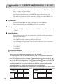
● C11 to 18 (external switch input operation type)
Input is performed in binary in the case of SP set and recipe set switching.
Example: When RSW 3 to 5 are used when switching eight sets
RSW5 RSW4
SP1
SP2
SP3
SP4
SP5
SP6
SP7
SP8
OFF
OFF
OFF
OFF
ON
ON
ON
ON
OFF
OFF
ON
ON
OFF
OFF
ON
ON
RSW3
OFF
ON
OFF
ON
OFF
ON
OFF
ON
1: RUN/READY (all channels)
2: Auto-tuning start/stop (all channels)
Use DMC10 version 7.XX onwards.
● C19 (number of user-defined items)
This item allows you to add up to 20 parameters from the entire DMC10 parameters in addition to existing items on the DMC10 setting change screen.
No additions are made when this item is set to “0”.
When “1” or more is set, set the desired items as related parameters are displayed
from C30 onwards.
15
● C20 (number of additional buffers)
This item allows you to add up to ten data items on currently connected DMC10s
in addition to currently buffered data. No additions are made when this item is set
to “0”.
When “1” or more is set, set the desired items as related parameters are displayed
from C90 onwards.
● C21 (number of recipe items)
This item is for setting the number of parameter types on the DMC10s per recipe.
Up to 199 parameters can be set.
When the parameter items are different on each DMC10, execute this item by the
total number of parameters in question for all DMC10s.
Example: If SP only is set for the 1st DMC10 and P, I and D are set for the 2nd
DMC10, the number of recipe items to set here in this item is four (SP,
P, I and D).
● C22 (number of recipe sets)
This item is for setting the number of recipe sets (maximum 99). Set so that the
following restriction is satisfied:
Number of recipe items (C21) x number of recipe sets (C22) x number of
DMC10 units ≤ 2860
● C23 (DMC10 setup screen display settings)
You can hide any desired item on the DMC10 setup screen.
This setting is made by setting the corresponding bits. Refer to the example
shown below to make the setting.
Example: If you want to hide AT, P, I and D, set C23 to 001Eh by setting each bit
as follows:
bit 0=0, bit 1=1, bit 2=1, bit 3=1, bit 4=1, bit 5=0
● C27 (execute automatic detection)
When setting this item, it is presumed that all DMC10s have finished being set
up, and that setup items C01 to C22 on the SDU10 have been completed.
Executing this item stores the information of DMC10s currently connected to the
SDU10 internally on the SDU10. Execute this item again when the settings of
the DMC10s have been changed after this item has been executed.
During execution of this item, the display blinks, and blinking stops within 2min
at most after execution is completed.
● C28 (automatic detection results)
This item allows you to check the number of currently connected DMC10s after
execution of automatic detection (C27) is completed.
● C29 (version information)
You can get the version information of the firmware.
This item displays the current version as long as the version is a new one (i.e. version 3.10 or later). However, the old version (i.e. version 3.02 or earlier) is not
displayed.
16
● C30 to C49 (user-defined item addresses)
This item is for setting the item address Nos. to be added.
For a list of addresses, see Modular Controller DMC10 User’s Manual
Description of Functions CP-UM-5143E.
● C50 to C69 (user-defined item name)
This item is for setting the names of items actually displayed in setting screen.
The characters and symbols in “Appendix 1. USER-DEFINED ITEM NAMES”
(page 27) can be used.
● C70 to C89 (user-defined item decimal point)
This item is for setting a decimal point if decimal point information is required
for numbers in screens that are set by setup items C50 to C69.
The information set here is for display only.
● C90 to C99 (additional buffering addresses)
“Additional buffering addressing” is a handy function for reading required parameters by host communications.
SDU10 is provided with memory area for storing the latest data. Data required
for running of the SDU10 is stored on the SDU10 at all times. This data is called
“buffered parameters.”
In addition to already determined parameter types (PV, SP, alarm states, etc.), up
to ten extra types of parameters can be defined as desired as buffered parameters
for each DMC10 unit.
As the parameters that are handled by host communications are arranged continuously on SDU10 internal memory, these buffered parameters can be read from
the host device using the minimum number of commands.
Normally, buffered parameters are read from the DMC10 at roughly 15-second
cycles and are updated. However, it sometimes takes 30 seconds or more to read
buffered parameters, for example, during writing of recipes.
For a list of addresses, see Modular Controller DMC10 User’s Manual
Description of Functions CP-UM-5143E.
● C101, C107 (event setting value A)
An event setting value. This is effective while the event operation type has been
set to 8.
If the minimum PV value went down below this value, the event becomes an ON
condition.
● C102, C108 (event setting value B)
An event setting value. This is effective while the event operation type has been
set to 8.
If the maximum PV value exceeded this value, the event becomes an ON condition.
17
● C103, C109 (Position of decimal point in event setting value A)
The positional information of the decimal point for the event setting value A. This
is effective while the event operation type has been set to 8.
A comparison is made between the minimum PV value and the event setting
value A with this positional information of decimal point.
● C104, C110 (Position of decimal point in event setting value B)
The positional information of the decimal point for the event setting value B. This
is effective while the event operation type has been set to 8.
A comparison is made between the maximum PV value and the event setting
value B with this positional information of decimal point.
● C105, C111 (event standby)
The "event standby" is a function to prevent an event in use from being turned on
even if the event is satisfying the ON condition when the power is turned on.
It functions when the ON condition is satisfied again after the OFF condition was
satisfied once.
● C106, C112 (event ON delay)
You can set the delay time after an event has satisfied the ON condition until it is
actually turned on in seconds.
18
■ List of SDU10 Recipe Items
Function
Prompt
r1
r2
r3
r4
r5
Recipe item 1
Recipe item 2
Recipe item 3
Recipe item 4
Recipe item 5
r199
Recipe item 199
Item
M: Setting enabled when in the Master mode
Factory Master/
Setting Slave
256
M
Description
Refer to the DMC10 User’s Manual.
Set the parameter addresses of the connected DMC10 for r1 to r199 (recipe
items).
■ List of SDU10 Recipe Sets
Function
Prompt
rf1
rf2
rf3
rf4
rf5
Recipe set 1
Recipe set 2
Recipe set 3
Recipe set 4
Recipe set 5
rf99
Recipe set 99
Item
M: Setting enabled when in the Master mode
Description
0: Disabled
1: Start reading of parameters rf1 to rf99 from the connected
DMC10.
Factory Master/
Setting Slave
0 M
Start reading of the recipe items from the DMC10 connected here for rf1 to rf199
(recipe sets).
Execute reading at the set No. of the recipe in question.
Setting “1” starts reading, and the display blinks. When reading ends, blinking
stops.
Setting “0” disables that recipe set No.
■ DMC10 Monitoring
Function Prompt
Item
Upper display:PV value
Basic display
Lower display:SP value or PV value
Upper display:SP value
Lower display:SP value
SP display
Upper display:
Lower display:CT1 value
Upper display:
Lower display:CT 2 value
Upper display: Max. PV value
Lower display: Min. PV value
Upper display:
Lower display:SP set value
Upper display:
Lower display:Recipe set value
CT1 current value
CT2 current value
Min./max. PV values
of all DMCs
SP set switching
display
Recipe set switching
display
Description
Display details can also be displayed
by setting C06 on SDU10.
Can also be displayed on slave units.
Displays only when basic display is PV
(upper display) and PV (lower display).
Can also be displayed on slave units.
Displayed only on model Nos. with CT.
Can also be displayed on slave units.
Displayed only on model Nos. with CT.
Factory
Setting
–
Remarks
–
C06: XXX2
–
C06: XX1X or
C06: XX3X
C06: XX1X or
C06: XX3X
C06: XX2X or
C06: XX3X
C06: XX1X or
C06: XX3X
C06: XX2X or
C06: XX3X
–
–
Enabled by multi-SP use on DMC10
1
Enabled by setting C22 on SDU10
1
19
■ Item Descriptions
● Basic display
“– – – –” is displayed on both the upper and lower displays when the SDU10 is
turned ON for the first time.
As the SDU10 does not have any information on currently connected DMC10s,
execute automatic detection (C27) after SDU10 setup is completed.
When the SDU10 is turned ON again after monitoring of DMC10s is enabled,
the current values of the modules and channels that were last displayed are displayed.
For the PV values of currently monitored DMC10s, the PV value and PV alarm
are displayed alternately if a sensor line break or other malfunction occurs.
To shift between the basic display displays in DMC10 address order (ascending
order), press the CH key.
● SP display
Display of SP on the upper and lower displays is enabled only when PV is set for
the upper and lower displays in the basic display. Press the PARA key in the PV
value display mode.
Set the basic display in the Run mode (C06).
To shift between the basic display displays in DMC10 address order (ascending
order), press the CH key.
● CT1, CT2 current value
This screen can be displayed by setting the Run mode (C06).
To shift between the CT displays in DMC10 address order (ascending order),
press the CH key.
If, during display, there is a DMC10 that does not support CT input, that DMC10
is skipped.
● Min./max. PV value display
This screen can be displayed by setting the Run mode (C06).
The “min./max. PV value display” is a function for simultaneously displaying the
minimum and maximum values from among the PV value of all channels on all
DMC10s currently connected to the SDU10.
This function can be used, for example, to check whether or not the temperature
distribution width of control targets such as chambers or glass substrates that are
heated at multiple locations is within predetermined values.
The current minimum and maximum values are displayed. This item can be set to
hold peak values after the SDU10 is turned ON. Minimum and maximum values
can be cleared either by pressing the CH key or external switch inputs.
● SP set switching display
On 2-channel DMC10 models, the SP sets can be changed within the range 1 to
8, and on 4-channel models within the range 1 to 4.
● Recipe switching display
Recipes can be switched up to the value set at number of recipe sets (C22).
Note
For details on the slave functions, see “Appendix 2. USE OF AN SDU10 AS A
SLAVE” (page 28).
20
■ Changing DMC10 Settings
Function
Prompt
SP or SP1
SP2
SP3
SP4
SP5
SP6
SP7
SP8
SP A
SP value or SP1 value
SP2 value
SP3 value
SP4 value
SP5 value
SP6 value
SP7 value
SP8 value
All the SP values in use
AT
P
Auto-tuning start/stop
Proportional band
I
Reset time
D
Rate time
PbIA
PV vias
CF1
Number of user-defined
items 1
Number of user-defined
items 2
Number of user-defined
items 3
Number of user-defined
items 4
Number of user-defined
items 5
Number of user-defined
items 6
Number of user-defined
items 7
Number of user-defined
items 8
Number of user-defined
items 9
Number of user-defined
items 10
Number of user-defined
items 11
Number of user-defined
items 12
Number of user-defined
items 13
Number of user-defined
items 14
Number of user-defined
items 15
Number of user-defined
items 16
Number of user-defined
items 17
Number of user-defined
items 18
Number of user-defined
items 19
Number of user-defined
items 20
CF2
CF3
CF4
CF5
CF6
CF7
CF8
CF9
CF10
CF11
CF12
CF13
CF14
CF15
CF16
CF17
CF18
CF19
CF20
Item
Factory
Setting
Differs according to setting of single-/multi-SP on DMC10
–
–
–
–
–
–
–
–
Simultaneously sets the SP values used by all the
–
channels of all the modules.
Starts/stops auto-tuning of currently displayed channel.
–
Changes setting of P (proportional band) of currently
–
displayed channel.
Changes setting of D (reset time) of currently displayed
–
channel.
Changes setting of I (rate time) of currently displayed
–
channel.
Changes setting of PV vias of currently displayed
–
channel.
Enabled by setting of number of user-defined items
–
(C19)
–
Description
Remarks
Displayed
only on
2-channels
DMC10 models
C30, C50, C70
must be set.
C31, C51, C71
must be set.
–
C32, C52, C72
must be set.
–
C33, C53, C73
must be set.
–
C34, C54, C74
must be set.
–
C35, C55, C75
must be set.
–
C36, C56, C76
must be set.
–
C37, C57, C77
must be set.
–
C38, C58, C78
must be set.
–
C39, C59, C79
must be set.
–
C40, C60, C80
must be set.
–
C41, C61, C81
must be set.
–
C42, C62, C82
must be set.
–
C43, C63, C83
must be set.
–
C44, C64, C84
must be set.
–
C45, C65, C85
must be set.
–
C46, C66, C86
must be set.
–
C47, C67, C87
must be set.
–
C48, C68, C88
must be set.
–
C49, C69, C89
must be set.
21
■ Item Descriptions
● SP (SP1 to 8)
The SP is only displayed when single-SP use is set on the DMC10s.
When multi-SP use is enabled, SP1 to 8 are displayed on 2-channel DMC10 models, and SP1 to 4 are displayed on 4-channel DMC10 models.
● SP A (All the SP values in use)
The SPs in use on all the DMC10 units connected to the SDU10 can be changed
by one operation.
● AT (auto-tuning start/stop)
This item is for starting/stopping auto-tuning on the currently displayed channel.
● P (proportional band)
This item is for changing the P (proportional band) setting of the currently displayed channel.
● I (reset time)
This item is for changing the I (reset time) setting of the currently displayed channel.
● D (rate time)
This item is for changing the D (rate time) setting of the currently displayed channel.
● PbIA (PV vias)
This item is for changing the PV vias setting of the currently displayed channel.
● CF1 to CF20 (user-defined items)
These items are enabled by setting SDU10 setup C19.
To use these functions, set setups C19 and C30 to C89.
22
6. RECIPE FUNCTION
■ Introduction
On the SDU10, each of the setup parameters can be provided with up to 99 files
called “recipes.” Recipes can be used to change the setup parameters (temperature
setting, alarm values, control parameters, etc.) by a single batch operation on multiple DMC10 by individual model. Recipes can be switched to by the front panel
keys on the SDU10, by external switch input from the SDU10, and by host communications.
■ Specifications
Max. number of recipes: 99
Max. number of parameter types/recipes: 199
Note, however, that the following restriction applies:
Number of recipes x parameter types x number of DMC10 units ≤ 2860
■ Setup Procedure
● Setting the parameter type (r1 to r199)
Set the DMC10 parameter types to be saved to recipes. Specify the parameter
type by the DMC10’s internal word address No.
● Reading and saving parameters
DMC10 internal parameter values are read to SDU10 for each recipe (1 to 99),
and read parameters are saved within recipes.
Handling Precautions
Recipe parameters can be set only when they have been read from a DMC10. To
change data in recipes, change the parameters held internally on the DMC10,
and read the parameters again.
■ Method of Use
Setup recipe parameters are written in a single operation to the target DMC10 by
specifying the recipe No. on the keys on the front panel of the SDU10, external
switch input or by communications.
Use the following formula to calculate the approximate time it takes to complete
writing of recipe parameters to each DMC10:
{30 x (number of parameter items per recipe) + 40} x (number of DMC10 units)
Unit: ms
Handling Precautions
• The above figure is merely a guideline, and may increase depending on the
operation circumstances of the SDU10. In particular, the communications time
increases when the external switch input function is used and slave devices are
used. When recipes are written by operating the keys on the front panel of the
SDU10, the recipe set No. blinks during writing. For this reason, when writing
recipes by external switch input or communications, measure the time it takes
to write the recipes by operating the keys on the front panel of the SDU10, and
use this value as reference.
• The communications time increases if wiring trouble, for example, prevents successful communications between the DMC10 and SDU10. Make sure that communications errors are not occurring.
23
7. HOST COMMUNICATIONS FUNCTION
The SDU10 is equipped with an RS-485 host communications function as part of the standard
specification. This function allows the user to communicate with a host device such as a personal
computer, PLC or Yamatake Corporation EST240Z touch panel using a program created by the user.
■ Features
• Up to 31 SDU10s can be connected to a single host device.(For the MODBUS, maximum
15 units)
When 16 or more DMC10s are to be used, DMC10s can be added on by using the SDU10.
• The CMC10L (sold separately) is required when the communications specifications of the
host device conforms to the RS-232C interface.
• For details on the communications parameters of SDU10, see “Appendix 4. SDU10
COMMUNICATIONS PARAMETER TABLES” (page 31).
• A wide range of communications commands are available to enable accessing of remote
parameters by a single command. The same commands as those for the DMC10 are supported.
• Some of the data of currently connected DMC10s is buffered. For this reason, DMC10
data can be easily accessed by accessing SDU10 internal parameters. Also, up to ten extra
parameters can be buffered.
SDU10 setups C20 and C90 to C99 must be set.
■ Specifications
SDU10 host communications is the same as DMC10 communications specifications except the cautions for the device address described as follows. (These are
two ways of specifying the device address on the SDU10.)
For details, refer to Modular Controller DMC10 User’s Manual Description of
Functions CP-UM-5143E, Chapter 10. Communications Functions.
• Example 1: When sub-addresses are not used
• Example 2: When sub-addresses are used
Features: - Common communications software from the host device is used
regardless of whether or not an SDU10 is included in the configuration.
15 or fewer DMC10s are used.
Specifications: - DMC10 device addresses shall be unique.
- The device address of the SDU10 shall be “0”.
- The addresses of commands from the host device shall be as
follows:
Device address: Device address of DMC10
Sub address:
“00”
Note:
- The addresses of commands from the host device shall be as follows.
Note, however, that a multi-drop configuration such as that shown in
figure below is not allowed.
Device address: “FE”
Sub address:
“00”
- For the MODBUS, set the DMC10 address to the device address.
PC
Device
address: 0
PC
Device
SDU10 address: 0
SDU10
Device
SDU10 address: 2
SDU10
Device
address: 1
DMC10
DMC10
4
ADR 0
4
LDR
ADR 0
8
C
CH3
PWR
16
22
17
23
18
24
19
25
20
CH4
21
22
23
24
25
23
24
25
ADR 0
PWR
22
17
23
18
24
24
19
25
25
20
CH4
CH2
21
22
22
22
23
23
23
24
24
23
19
24
20
25
21
21
22
22
23
23
24
25
25
DMC10
DMC10
3
DMC10
DMC10
4
ADR 0
PWR
17
18
19
20
23
24
25
ADR 0
PWR
22
17
23
18
24
24
19
25
25
20
CH4
CH2
21
22
22
22
23
23
23
24
24
23
19
24
20
25
21
21
22
22
23
23
24
25
25
DMC10
DMC10
9
4
ADR 0
PWR
17
18
19
20
ADR 0
23
24
25
16
17
23
18
18
24
24
19
19
25
25
20
21
22
23
24
25
2
CH4
CH2
21
21
22
22
23
23
24
17
18
24
25
22
22
23
23
19
20
CH4
24
25
25
DMC10
DMC10
3
16
23
21
23
24
25
DMC10
2
LDR
8
C
CH3
CH1
PWR
CH1
21
16
16
22
22
17
17
23
23
18
18
24
24
19
19
25
25
20
20
CH4
22
4
ADR 0
PWR
21
CH2
21
LDR
8
C
CH3
CH1
22
21
CH2
24
25
ADR 0
PWR
21
20
25
24
4
LDR
8
C
CH3
CH1
22
17
23
DMC10
Device address: 1
4
ADR 0
PWR
21
16
22
CH4
22
CH1
LDR
8
C
CH3
PWR
21
CH2
21
4
LDR
8
C
CH3
CH1
16
CH4
24
25
8
22
18
25
24
25
21
17
CH2
21
21
16
LDR
8
C
CH3
CH1
21
16
23
DMC10
7
4
LDR
8
C
CH3
CH1
22
CH4
22
ADR 0
PWR
21
CH2
21
4
LDR
8
C
CH3
CH1
16
CH4
24
25
2
22
18
25
24
25
21
17
CH2
21
21
16
LDR
8
C
CH3
CH1
21
16
23
DMC10
Device address: 1
4
LDR
8
C
CH3
CH1
22
CH4
22
ADR 0
PWR
21
CH2
21
4
LDR
8
C
CH3
CH1
21
24
Feature: - 16 or more DMC10 units can be used.
Specifications: - The same DMC10 device address can be
used on different SDU10s.
- The addresses of commands from the
host device shall be as follows:
Device address: Address of SDU10
Device address of DMC10
Sub address:
Note: - The addresses for accessing SDU10 internal data
shall be as follows:
Device address: Address of SDU10
Sub address:
“00”
- For the MODBUS, the one group of upper 4 bits in
the device address is the SDU10 address. Another
group of lower 4 bits is the DMC10 address.
CH4
CH2
CH2
21
21
21
21
22
22
22
22
23
23
23
23
24
24
24
24
25
25
25
25
DMC10
DMC10
3
4
Handling Precautions
• When accessing the DMC10 from the host device via the SDU10, pay attention
to the following time-out setting condition. Accessing of SDU10 data is determined by SDU10 setup C04.
Condition: Set the time-out for when there is no response to at least 1s.
• Use example 1 above when using the EST240Z DMC10 package.
8. ALARM CODES
Alarms on the SDU10 can be identified by alarm lamps when an error occurs on connected
DMC10s and on the SDU10.
DMC10 alarm codes can also be viewed on the upper and lower displays.
■ Alarm Lamp Indications
Lamps State
Cause
Countermeasure
Remarks
AL1 Blinking Display unit communications • Check for miswiring or broken communications line.
error
• Check communications conditions.
• A DMC10 is not responding. • Check for changes to DMC10 settings after automatic
• A DMC10 returns the
detection.
abnormal end code.
• Slave response time is longer than time-out. (Check
setup C08.)
• Check additional setting items or recipe addresses.
Lit Display unit memory error
Request SDU10 repair.
• SDU10 memory is damaged.
AL2
Blinking DMC10 PV error
• Operate the [CH] key to check for any DMC10s for
For details
• A PV-related alarm is
which ALXX is alternately displayed.
of ALXX,
established on a DMC10.
• Follow the description in the DMC10 User’s Manual.
see table
below.
Lit DMC10 memory error
• Operate the [CH] key to check for any DMC10s for
For details
• A DMC10 memory error is
which ALXX is alternately displayed.
of ALXX,
occurring
• Follow the description in the DMC10 User’s Manual.
see table
below.
■ DMC10 Alarm Codes
Display
Cause
Countermeasure
AL01 PV upper limit alarm has occurred on Follow the description in the DMC10 User’s Manual.
currently displayed DMC10 channel.
AL02 PV lower limit alarm has occurred on
currently displayed DMC10 channel.
AL03 CJ error/BC line alarm has occurred
on currently displayed DMC10 channel.
AL70 A/D alarm has occurred on currently
displayed DMC10 channel.
AL96 EEPROM error has occurred on
currently displayed DMC10.
AL97 Adjustment RAM error has occurred
on currently displayed DMC10.
AL98 Setting RAM error has occurred on
currently displayed DMC10.
Remarks
■ Other Error Indications
Display State
Cause
Loc
Lit for Key lock is set.
1s
Err
Lit for Settings could not be written
1s on the DMC10 Setting
screen because of a
communications error.
---Lit There is no display data as a
communications error has
occurred.
(no-response/abnormal end
code)
...
Lit
PV value and SP value
cannot be displayed.
Countermeasure
Set setup C01 to “0: Key lock not engaged.”
Remarks
• When DMC10 additional setting items are being
implemented, check the set addresses.
• Check the DMC10 mode and other settings.
• Make sure that automatic detection is being executed.
• Check for changes to DMC10 settings after automatic
detection.
• Check the DMC10 power supply.
• Check for miswiring and broken lines.
• Check the communications conditions of the SDU10
and DMC10.
• Set a larger value to setup C08 (slave time-out)
The PV and SP values are not displayed for channels
that fall under the following categories:
• Channels to which the PV input type of the DMC10 is “0”
• Channels that are used as RSP
• Channels that are used for feeding back the motor drive
25
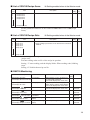
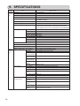
9. SPECIFICATIONS
Category
Item
General
Model No.
Specifica- Memory backup
tions
Rated power supply voltage
Power consumption
Insulation resistance
Dielectric strength
Inrush current (power ON)
Isolation
Operating conditions Ambient temperature
Ambient humidity
Power voltage
Vibration resistance
Impact resistance
Transport/storage
Ambient temperature
Ambient humidity
Package drop
Mass
Terminal screw tightening torque
Applicable standards
Case material / color
Additional External switch input No. of points
SpecificaFunctions
tions
Allowable ON
contact resistance
Allowable OFF
contact resistance
Allowable ON
residual voltage
Open terminal
voltage
ON terminal current
Event output
No. of points
Functions
Output type
OFF leakage
current
ON output voltage
Output rating
Host/slave
Signal level
communications
Transmission path
connection
Communication
system
Max. line length
Terminating
resistor
26
Specifications
SDU10T0100
Non-volatile semiconductor memory
24Vdc
Max. 3W
Across power terminal and secondary terminals: 20MΩ min.
(by 500Vdc megger)
Across power terminal and secondary terminals: 500Vac, 1min.
Max. 10A
• Across power circuit and secondary side circuit
• Across host communications and slave communications
• Non-isolation across slave communications and RSW/EVENT
0 to 50°C
10 to 90%RH
21.6 to 26.4Vdc
0 to 2m/s2
0 to 10m/s2
–20 to +70°C
10 to 95%RH
60cm
Max. 200g
Max. 0.25N•m
EN61000-6-4, EN61000-6-2, IP65 equivalent
PC resin / Light gray (Muncell: 2.5Y7.5/1 equivalent)
8 (2 of which are shared with events)
See SDU10 setups C11 to C18.
Max. 250Ω
Min. 100kΩ
Max. 1V
5Vdc
Approx. 4mA
2 (shared use with external switch input)
See SDU10 setups C09 and C10.
Open-collector
Max. 100μA
Max. 1V
Max. 30Vdc (External power), Max. 70mA
RS-485 compliant
Multi-point (host: max. 31 units, slave: max. 15 units DMC10)
Half duplex, asynchronous
Max. 500m
External resistor must not be attached as equivalent terminating resistance is built-in.
Appendix 1. USER-DEFINED ITEM NAMES
In addition to the existing setup items, up to 20 extra items can be added on to the DMC10’s setting items.
These items are set in SDU10 setups C50 to C69 (user-defined item name). (For details, see
page 17.)
After a setting item has been added, it can be assigned a name (symbol) up to four character
long.
The symbols can be used for the name and displayed are as follows.
Pressing the
or
keys in SDU10 setups C50 to C69 (user-defined item name)
moves the selection cyclically as follows. (When a symbol stops blinking and stays lit, this indicates that the symbol has been applied.)
Space
Space
key
key
Space
Space
27
Appendix 2. USE OF AN SDU10 AS A SLAVE
■ Purpose
The PV value for up to two channels can be displayed as the SDU10 has two displays, an upper and lower display.
Adding on another SDU10 as a slave enables the PV values for four channels to
be monitored simultaneously (when DMC10s on four channels are used).
The number of points can also be extended by adding on another SDU10 as a
slave when there are not enough external switch inputs or event terminals.
■ Connection
Connect the SDU10 for the slave to the same line as the DMC10.
Host communications on the SDU10 for the slave is disabled.
■ Setup
Before the SDU10 is to be used as a slave, the SDU10 setup C02 must be set to
“1: Slave”.
■ Specifications
Items displayed on the slave are automatically matched with the items that are
displayed on the master.
Only the items shown below are displayed. Other items are not displayed.
Also, DMC10 settings cannot be changed on the slave.
The external switch inputs and events provided on the slave can be used in the
same way on the master.
• Basic display
• SP display
• CT display
Handling Precautions
•If the master-slave function is used while SDU10 units of old version and new
version are used together, the operation may be unstable.
For identification of the old and new versions, see ●C29 (version information)
(on page 16).
•You can change the display contents of the master and the slave using the CH
key on the SDU10 for the master. The CH key and the RDY key on the SDU10
for the slave are not available. The items to be displayed on the master and the
slave are predefined. You cannot operate the displays on the master and the
slave individually nor display the same contents on both the unit.
•The tables below show the items to be displayed on the devices while a slave is used.
Items displayed when PV/PV display has been selected Items displayed when PV/SP display has been selected
display
Master
display
Slave
display
28
Upper
Lower
Upper
Lower
2CH Model 4CH Model
display
display
PV1 value
PV2 value
None
None
PV1 value
PV2 value
PV3 value
PV4 value
display
Master
display
Slave
display
Upper
Lower
Upper
Lower
2, 4CH Model 4CH Model
display
display
PV1 value
SP1 value
PV2 value
SP2 value
PV3 value
SP3 value
PV4 value
SP4 value
Appendix 3. SDU10 INTERNAL SETUP DATA BATCH COPY FUNCTION
This function is for transferring all setup data from the SDU10 to another SDU10.
This function comes in useful for copying all setup data to a spare SDU10 instead of storage
media for saving all SDU10 settings or setting up a new SDU10 unit.
Handling Precautions
Do not use the copy function between an old version SDU and a new version
SDU. For identification of the old and new versions, see ●C29 (version information) (on page 16).
■ Download
Perform this procedure to batch-transfer all setting data already saved on a spare
SDU10 to an SDU10 newly added to the configuration.
(1)Connect the receiving SDU10 and sending SDU10 for host communications.
Note: Disable host communications on the SDU10 newly added to the configuration if host communications is already enabled.
(2)Turn ON the receiving SDU10.
(3)Turn the sending SDU10 ON with its CH key held down.
If the following does not appear on the display on the sending SDU10, perform this step again.
PV
No
CH
SP
F1
F2
F3
RDY
F4 AL1 AL2
CH
CH
MAN
AT
RDY
MAN
AT
RDY
PARA
SDU10
(4)Press the PARA key to start the batch transfer.
During the transfer, Send blinks on the lower display on the sending SDU10,
and rEcv is displayed on the receiving SDU10.
If the transfer ends successfully, Fin is lit on the lower display on the sending
SDU10, and the display on the receiving SDU10 changes to the regular display.
If the transfer ends in error, err is lit on the lower display on the sending
SDU10, and the display on the receiving SDU10 changes to the regular display.
(5)When the transfer ends successfully, turn ON the receiving SDU10 again.
29
■ Upload
Perform this procedure to save all SDU10 setting data to a spare SDU10.
(1)Connect the receiving SDU10 and sending SDU10 for host communications.
Note: Disable host communications on the SDU10 newly added to the configuration if host communications is already enabled.
(2)Turn ON the sending SDU10.
(3)Turn the receiving SDU10 ON with its CH key held down.
If the following does not appear on the display on the receiving SDU10, perform this step again.
PV
No
CH
SP
F1
F2
F3
RDY
F4 AL1 AL2
CH
CH
MAN
AT
MAN
AT
RDY
RDY
PARA
SDU10
(4)Press the
key to set the display as follows on the receiving SDU10.
PV
No
CH
SP
F1
F2
F3
RDY
F4 AL1 AL2
CH
CH
MAN
AT
MAN
AT
RDY
RDY
PARA
SDU10
(5)Press the PARA key to start the batch transfer.
During the transfer, rEcv blinks on the lower display on the receiving SDU10,
and Send is displayed on the sending SDU10.
If the transfer ends successfully, Fin is lit on the lower display on the receiving
SDU10, and the display on the sending SDU10 changes to the regular display.
If the transfer ends in error, err is lit on the lower display on the receiving
SDU10, and the display on the sending SDU10 changes to the regular display.
30
Appendix 4. SDU10 COMMUNICATIONS PARAMETER TABLES
■ SDU10 Setup Items
R: Read, W: Write
«: Available, ✕: Not available
Function
Item
Prompt
C01 Key lock
Address
RAM ROM
RAM ROM R W R W
1001 5001 « « « «
Function
Item
Prompt
C51 User-defined item 2 name
Address
RAM ROM
RAM ROM R W R W
1203 5203 « « « «
C02
Slave device setting
1002 5002 « « « «
C52
User-defined item 3 name
1205 5205 « « « «
C03
Device address
1003 5003 « « « «
C53
User-defined item 4 name
1207 5207 « « « «
C04
Host communications settings 1004 5004 « « « «
C54
User-defined item 5 name
1209 5209 « « « «
C05
Slave communications settings 1005 5005 « « « «
C55
User-defined item 6 name
1211 5211 « « « «
C06
Display method in Run mode 1006 5006 « « « «
C56
User-defined item 7 name
1213 5213 « « « «
C07
LED operation type
1007 5007 « « « «
C57
User-defined item 8 name
1215 5215 « « « «
C08
RDY key function
1008 5008 « « « «
C58
User-defined item 9 name
1217 5217 « « « «
C09
Event 1 operation type
1009 5009 « « « «
C59
User-defined item 10 name 1219 5219 « « « «
C10
Event 2 operation type
1010 5010 « « « «
C60
User-defined item 11 name 1221 5221 « « « «
C11
External switch input 1 operation type 1011 5011 « « « «
C61
User-defined item 12 name 1223 5223 « « « «
C12
External switch input 2 operation type 1012 5012 « « « «
C62
User-defined item 13 name 1225 5225 « « « «
C13
External switch input 3 operation type 1013 5013 « « « «
C63
User-defined item 14 name 1227 5227 « « « «
C14
External switch input 4 operation type 1014 5014 « « « «
C64
User-defined item 15 name 1229 5229 « « « «
C15
External switch input 5 operation type 1015 5015 « « « «
C65
User-defined item 16 name 1231 5231 « « « «
C16
External switch input 6 operation type 1016 5016 « « « «
C66
User-defined item 17 name 1233 5233 « « « «
C17
External switch input 7 operation type 1017 5017 « « « «
C67
User-defined item 18 name 1235 5235 « « « «
C18
External switch input 8 operation type 1018 5018 « « « «
C68
User-defined item 19 name 1237 5237 « « « «
C19
Number of user-defined items 1019 5019 « « « «
C69
User-defined item 20 name 1239 5239 « « « «
C20
Number of additional buffers 1020 5020 « « « «
C70
User-defined item 1 decimal point 1301 5301 « « « «
C21
Number of recipe items
1021 5021 « « « «
C71
User-defined item 2 decimal point 1302 5302 « « « «
C22
Number of recipe sets
1022 5022 « « « «
C72
User-defined item 3 decimal point 1303 5303 « « « «
C23
DMC10 setup screen display settings 1023 5023 « « « «
C73
User-defined item 4 decimal point 1304 5304 « « « «
C27
Execute automatic detection 1027 5027 « « ✕ ✕
C74
User-defined item 5 decimal point 1305 5305 « « « «
C28
Automatic detection results 1028 5028 « ✕ ✕ ✕
C75
User-defined item 6 decimal point 1306 5306 « « « «
C29
Version information
1029 5029 « ✕ ✕ ✕
C76
User-defined item 7 decimal point 1307 5307 « « « «
C30
User-defined item 1 address 1101 5101 « « « «
C77
User-defined item 8 decimal point 1308 5308 « « « «
C31
User-defined item 2 address 1102 5102 « « « «
C78
User-defined item 9 decimal point 1309 5309 « « « «
C32
User-defined item 3 address 1103 5103 « « « «
C79
User-defined item 10 decimal point 1310 5310 « « « «
C33
User-defined item 4 address 1104 5104 « « « «
C80
User-defined item 11 decimal point 1311 5311 « « « «
C34
User-defined item 5 address 1105 5105 « « « «
C81
User-defined item 12 decimal point 1312 5312 « « « «
C35
User-defined item 6 address 1106 5106 « « « «
C82
User-defined item 13 decimal point 1313 5313 « « « «
C36
User-defined item 7 address 1107 5107 « « « «
C83
User-defined item 14 decimal point 1314 5314 « « « «
C37
User-defined item 8 address 1108 5108 « « « «
C84
User-defined item 15 decimal point 1315 5315 « « « «
C38
User-defined item 9 address 1109 5109 « « « «
C85
User-defined item 16 decimal point 1316 5316 « « « «
C39
User-defined item 10 address 1110 5110 « « « «
C86
User-defined item 17 decimal point 1317 5317 « « « «
C40
User-defined item 11 address 1111 5111 « « « «
C87
User-defined item 18 decimal point 1318 5318 « « « «
C41
User-defined item 12 address 1112 5112 « « « «
C88
User-defined item 19 decimal point 1319 5319 « « « «
C42
User-defined item 13 address 1113 5113 « « « «
C89
User-defined item 20 decimal point 1320 5320 « « « «
C43
User-defined item 14 address 1114 5114 « « « «
C90
Additional buffering address 1 1401 5401 « « « «
C44
User-defined item 15 address 1115 5115 « « « «
C91
Additional buffering address 2 1402 5402 « « « «
C45
User-defined item 16 address 1116 5116 « « « «
C92
Additional buffering address 3 1403 5403 « « « «
C46
User-defined item 17 address 1117 5117 « « « «
C93
Additional buffering address 4 1404 5404 « « « «
C47
User-defined item 18 address 1118 5118 « « « «
C94
Additional buffering address 5 1405 5405 « « « «
C48
User-defined item 19 address 1119 5119 « « « «
C95
Additional buffering address 6 1406 5406 « « « «
C49
User-defined item 20 address 1120 5120 « « « «
C96
Additional buffering address 7 1407 5407 « « « «
C50
User-defined item 1 name
1201 5201 « « « «
C97
Additional buffering address 8 1408 5408 « « « «
31
■ SDU10 Recipe Items
Address
RAM ROM
Function
Item
Prompt
RAM ROM R W R W
C98 Additional buffering address 9 1409 5409 « « « «
Address
RAM ROM
RAM ROM R W R W
1501 5501 « « « «
Additional buffering address 10 1410 5410 « « « «
r2
Recipe item 2
1502 5502 « « « «
C101 Event 1 setting value A
1421 5421 « « « «
r3
Recipe item 3
1503 5503 « « « «
C102 Event 1 setting value B
1422 5422 « « « «
r4
Recipe item 4
1504 5504 « « « «
C103 Position of decimal point in 1423 5423 « « « «
event 1 setting value A
r5
Recipe item 5
1505 5505 « « « «
r6
Recipe item 6
1506 5506 « « « «
C104 Position of decimal point in 1424 5424 « « « «
event 1 setting value B
r7
Recipe item 7
1507 5507 « « « «
r8
Recipe item 8
1508 5508 « « « «
r9
Recipe item 9
1509 5509 « « « «
r10
Recipe item 10
1510 5510 « « « «
r11
Recipe item 11
1511 5511 « « « «
r12
Recipe item 12
1512 5512 « « « «
r13
Recipe item 13
1513 5513 « « « «
C110 Position of decimal point in 1430 5430 « « « «
event 2 setting value B
r14
Recipe item 14
1514 5514 « « « «
r15
Recipe item 15
1515 5515 « « « «
C111 Event 2 standby
1431 5431 « « « «
r16
Recipe item 16
1516 5516 « « « «
C112 Event 2 ON delay
1432 5432 « « « «
r17
Recipe item 17
1517 5517 « « « «
r18
Recipe item 18
1518 5518 « « « «
r19
Recipe item 19
1519 5519 « « « «
r20
Recipe item 20
1520 5520 « « « «
r21
Recipe item 21
1521 5521 « « « «
r22
Recipe item 22
1522 5522 « « « «
r23
Recipe item 23
1523 5523 « « « «
r24
Recipe item 24
1524 5524 « « « «
r25
Recipe item 25
1525 5525 « « « «
r26
Recipe item 26
1526 5526 « « « «
r27
Recipe item 27
1527 5527 « « « «
r28
Recipe item 28
1528 5528 « « « «
r29
Recipe item 29
1529 5529 « « « «
r30
Recipe item 30
1530 5530 « « « «
r31
Recipe item 31
1531 5531 « « « «
r32
Recipe item 32
1532 5532 « « « «
r33
Recipe item 33
1533 5533 « « « «
r34
Recipe item 34
1534 5534 « « « «
r35
Recipe item 35
1535 5535 « « « «
r36
Recipe item 36
1536 5536 « « « «
r37
Recipe item 37
1537 5537 « « « «
r38
Recipe item 38
1538 5538 « « « «
r39
Recipe item 39
1539 5539 « « « «
r40
Recipe item 40
1540 5540 « « « «
r41
Recipe item 41
1541 5541 « « « «
r42
Recipe item 42
1542 5542 « « « «
r43
Recipe item 43
1543 5543 « « « «
r44
Recipe item 44
1544 5544 « « « «
r45
Recipe item 45
1545 5545 « « « «
r46
Recipe item 46
1546 5546 « « « «
r47
Recipe item 47
1547 5547 « « « «
r48
Recipe item 48
1548 5548 « « « «
r49
Recipe item 49
1549 5549 « « « «
r50
Recipe item 50
1550 5550 « « « «
C99
C105 Event 1 standby
1425 5425 « « « «
C106 Event 1 ON delay
1426 5426 « « « «
C107 Event 2 setting value A
1427 5427 « « « «
C108 Event 2 setting value B
1428 5428 « « « «
C109 Position of decimal point in 1429 5429 « « « «
event 2 setting value A
32
Function
Item
Prompt
r1
Recipe item 1
Function
Item
Prompt
r51 Recipe item 51
Address
RAM ROM
RAM ROM R W R W
1551 5551 « « « «
Function
Item
Prompt
r101 Recipe item 101
Address
RAM ROM
RAM ROM R W R W
1601 5601 « « « «
r52
Recipe item 52
1552 5552 « « « «
r102 Recipe item 102
1602 5602 « « « «
r53
Recipe item 53
1553 5553 « « « «
r103 Recipe item 103
1603 5603 « « « «
r54
Recipe item 54
1554 5554 « « « «
r104 Recipe item 104
1604 5604 « « « «
r55
Recipe item 55
1555 5555 « « « «
r105 Recipe item 105
1605 5605 « « « «
r56
Recipe item 56
1556 5556 « « « «
r106 Recipe item 106
1606 5606 « « « «
r57
Recipe item 57
1557 5557 « « « «
r107 Recipe item 107
1607 5607 « « « «
r58
Recipe item 58
1558 5558 « « « «
r108 Recipe item 108
1608 5608 « « « «
r59
Recipe item 59
1559 5559 « « « «
r109 Recipe item 109
1609 5609 « « « «
r60
Recipe item 60
1560 5560 « « « «
r110 Recipe item 110
1610 5610 « « « «
r61
Recipe item 61
1561 5561 « « « «
r111 Recipe item 111
1611 5611 « « « «
r62
Recipe item 62
1562 5562 « « « «
r112 Recipe item 112
1612 5612 « « « «
r63
Recipe item 63
1563 5563 « « « «
r113 Recipe item 113
1613 5613 « « « «
r64
Recipe item 64
1564 5564 « « « «
r114 Recipe item 114
1614 5614 « « « «
r65
Recipe item 65
1565 5565 « « « «
r115 Recipe item 115
1615 5615 « « « «
r66
Recipe item 66
1566 5566 « « « «
r116 Recipe item 116
1616 5616 « « « «
r67
Recipe item 67
1567 5567 « « « «
r117 Recipe item 117
1617 5617 « « « «
r68
Recipe item 68
1568 5568 « « « «
r118 Recipe item 118
1618 5618 « « « «
r69
Recipe item 69
1569 5569 « « « «
r119 Recipe item 119
1619 5619 « « « «
r70
Recipe item 70
1570 5570 « « « «
r120 Recipe item 120
1620 5620 « « « «
r71
Recipe item 71
1571 5571 « « « «
r121 Recipe item 121
1621 5621 « « « «
r72
Recipe item 72
1572 5572 « « « «
r122 Recipe item 122
1622 5622 « « « «
r73
Recipe item 73
1573 5573 « « « «
r123 Recipe item 123
1623 5623 « « « «
r74
Recipe item 74
1574 5574 « « « «
r124 Recipe item 124
1624 5624 « « « «
r75
Recipe item 75
1575 5575 « « « «
r125 Recipe item 125
1625 5625 « « « «
r76
Recipe item 76
1576 5576 « « « «
r126 Recipe item 126
1626 5626 « « « «
r77
Recipe item 77
1577 5577 « « « «
r127 Recipe item 127
1627 5627 « « « «
r78
Recipe item 78
1578 5578 « « « «
r128 Recipe item 128
1628 5628 « « « «
r79
Recipe item 79
1579 5579 « « « «
r129 Recipe item 129
1629 5629 « « « «
r80
Recipe item 80
1580 5580 « « « «
r130 Recipe item 130
1630 5630 « « « «
r81
Recipe item 81
1581 5581 « « « «
r131 Recipe item 131
1631 5631 « « « «
r82
Recipe item 82
1582 5582 « « « «
r132 Recipe item 132
1632 5632 « « « «
r83
Recipe item 83
1583 5583 « « « «
r133 Recipe item 133
1633 5633 « « « «
r84
Recipe item 84
1584 5584 « « « «
r134 Recipe item 134
1634 5634 « « « «
r85
Recipe item 85
1585 5585 « « « «
r135 Recipe item 135
1635 5635 « « « «
r86
Recipe item 86
1586 5586 « « « «
r136 Recipe item 136
1636 5636 « « « «
r87
Recipe item 87
1587 5587 « « « «
r137 Recipe item 137
1637 5637 « « « «
r88
Recipe item 88
1588 5588 « « « «
r138 Recipe item 138
1638 5638 « « « «
r89
Recipe item 89
1589 5589 « « « «
r139 Recipe item 139
1639 5639 « « « «
r90
Recipe item 90
1590 5590 « « « «
r140 Recipe item 140
1640 5640 « « « «
r91
Recipe item 91
1591 5591 « « « «
r141 Recipe item 141
1641 5641 « « « «
r92
Recipe item 92
1592 5592 « « « «
r142 Recipe item 142
1642 5642 « « « «
r93
Recipe item 93
1593 5593 « « « «
r143 Recipe item 143
1643 5643 « « « «
r94
Recipe item 94
1594 5594 « « « «
r144 Recipe item 144
1644 5644 « « « «
r95
Recipe item 95
1595 5595 « « « «
r145 Recipe item 145
1645 5645 « « « «
r96
Recipe item 96
1596 5596 « « « «
r146 Recipe item 146
1646 5646 « « « «
r97
Recipe item 97
1597 5597 « « « «
r147 Recipe item 147
1647 5647 « « « «
r98
Recipe item 98
1598 5598 « « « «
r148 Recipe item 148
1648 5648 « « « «
r99
Recipe item 99
1599 5599 « « « «
r149 Recipe item 149
1649 5649 « « « «
1600 5600 « « « «
r150 Recipe item 150
1650 5650 « « « «
r100 Recipe item 100
33
■ SDU10 Recipe Sets
34
Function
Item
Prompt
r151 Recipe item 151
Address
RAM ROM
RAM ROM R W R W
1651 5651 « « « «
Function
Item
Prompt
rf1
Recipe set 1
Address
RAM ROM
RAM ROM R W R W
1701 5701 « « « «
r152 Recipe item 152
1652 5652 « « « «
rf2
Recipe set 2
1702 5702 « « « «
r153 Recipe item 153
1653 5653 « « « «
rf3
Recipe set 3
1703 5703 « « « «
r154 Recipe item 154
1654 5654 « « « «
rf4
Recipe set 4
1704 5704 « « « «
r155 Recipe item 155
1655 5655 « « « «
rf5
Recipe set 5
1705 5705 « « « «
r156 Recipe item 156
1656 5656 « « « «
rf6
Recipe set 6
1706 5706 « « « «
r157 Recipe item 157
1657 5657 « « « «
rf7
Recipe set 7
1707 5707 « « « «
r158 Recipe item 158
1658 5658 « « « «
rf8
Recipe set 8
1708 5708 « « « «
r159 Recipe item 159
1659 5659 « « « «
rf9
Recipe set 9
1709 5709 « « « «
r160 Recipe item 160
1660 5660 « « « «
rf10
Recipe set 10
1710 5710 « « « «
r161 Recipe item 161
1661 5661 « « « «
rf11
Recipe set 11
1711 5711 « « « «
r162 Recipe item 162
1662 5662 « « « «
rf12
Recipe set 12
1712 5712 « « « «
r163 Recipe item 163
1663 5663 « « « «
rf13
Recipe set 13
1713 5713 « « « «
r164 Recipe item 164
1664 5664 « « « «
rf14
Recipe set 14
1714 5714 « « « «
r165 Recipe item 165
1665 5665 « « « «
rf15
Recipe set 15
1715 5715 « « « «
r166 Recipe item 166
1666 5666 « « « «
rf16
Recipe set 16
1716 5716 « « « «
r167 Recipe item 167
1667 5667 « « « «
rf17
Recipe set 17
1717 5717 « « « «
r168 Recipe item 168
1668 5668 « « « «
rf18
Recipe set 18
1718 5718 « « « «
r169 Recipe item 169
1669 5669 « « « «
rf19
Recipe set 19
1719 5719 « « « «
r170 Recipe item 170
1670 5670 « « « «
rf20
Recipe set 20
1720 5720 « « « «
r171 Recipe item 171
1671 5671 « « « «
rf21
Recipe set 21
1721 5721 « « « «
r172 Recipe item 172
1672 5672 « « « «
rf22
Recipe set 22
1722 5722 « « « «
r173 Recipe item 173
1673 5673 « « « «
rf23
Recipe set 23
1723 5723 « « « «
r174 Recipe item 174
1674 5674 « « « «
rf24
Recipe set 24
1724 5724 « « « «
r175 Recipe item 175
1675 5675 « « « «
rf25
Recipe set 25
1725 5725 « « « «
r176 Recipe item 176
1676 5676 « « « «
rf26
Recipe set 26
1726 5726 « « « «
r177 Recipe item 177
1677 5677 « « « «
rf27
Recipe set 27
1727 5727 « « « «
r178 Recipe item 178
1678 5678 « « « «
rf28
Recipe set 28
1728 5728 « « « «
r179 Recipe item 179
1679 5679 « « « «
rf29
Recipe set 29
1729 5729 « « « «
r180 Recipe item 180
1680 5680 « « « «
rf30
Recipe set 30
1730 5730 « « « «
r181 Recipe item 181
1681 5681 « « « «
rf31
Recipe set 31
1731 5731 « « « «
r182 Recipe item 182
1682 5682 « « « «
rf32
Recipe set 32
1732 5732 « « « «
r183 Recipe item 183
1683 5683 « « « «
rf33
Recipe set 33
1733 5733 « « « «
r184 Recipe item 184
1684 5684 « « « «
rf34
Recipe set 34
1734 5734 « « « «
r185 Recipe item 185
1685 5685 « « « «
rf35
Recipe set 35
1735 5735 « « « «
r186 Recipe item 186
1686 5686 « « « «
rf36
Recipe set 36
1736 5736 « « « «
r187 Recipe item 187
1687 5687 « « « «
rf37
Recipe set 37
1737 5737 « « « «
r188 Recipe item 188
1688 5688 « « « «
rf38
Recipe set 38
1738 5738 « « « «
r189 Recipe item 189
1689 5689 « « « «
rf39
Recipe set 39
1739 5739 « « « «
r190 Recipe item 190
1690 5690 « « « «
rf40
Recipe set 40
1740 5740 « « « «
r191 Recipe item 191
1691 5691 « « « «
rf41
Recipe set 41
1741 5741 « « « «
r192 Recipe item 192
1692 5692 « « « «
rf42
Recipe set 42
1742 5742 « « « «
r193 Recipe item 193
1693 5693 « « « «
rf43
Recipe set 43
1743 5743 « « « «
r194 Recipe item 194
1694 5694 « « « «
rf44
Recipe set 44
1744 5744 « « « «
r195 Recipe item 195
1695 5695 « « « «
rf45
Recipe set 45
1745 5745 « « « «
r196 Recipe item 196
1696 5696 « « « «
rf46
Recipe set 46
1746 5746 « « « «
r197 Recipe item 197
1697 5697 « « « «
rf47
Recipe set 47
1747 5747 « « « «
r198 Recipe item 198
1698 5698 « « « «
rf48
Recipe set 48
1748 5748 « « « «
r199 Recipe item 199
1699 5699 « « « «
rf49
Recipe set 49
1749 5749 « « « «
rf50
Recipe set 50
1750 5750 « « « «
■ State Monitoring Data
Function
Item
Prompt
rf51 Recipe set 51
Address
RAM ROM
RAM ROM R W R W
1751 5751 « « « «
rf52
Recipe set 52
1752 5752 « « « «
rf53
Recipe set 53
1753 5753 « « « «
rf54
Recipe set 54
1754 5754 « « « «
rf55
Recipe set 55
1755 5755 « « « «
rf56
Recipe set 56
1756 5756 « « « «
rf57
Recipe set 57
1757 5757 « « « «
rf58
Recipe set 58
1758 5758 « « « «
rf59
Recipe set 59
1759 5759 « « « «
rf60
Recipe set 60
1760 5760 « « « «
rf61
Recipe set 61
1761 5761 « « « «
rf62
Recipe set 62
1762 5762 « « « «
rf63
Recipe set 63
1763 5763 « « « «
rf64
Recipe set 64
1764 5764 « « « «
rf65
Recipe set 65
1765 5765 « « « «
rf66
Recipe set 66
1766 5766 « « « «
rf67
Recipe set 67
1767 5767 « « « «
rf68
Recipe set 68
1768 5768 « « « «
rf69
Recipe set 69
1769 5769 « « « «
rf70
Recipe set 70
1770 5770 « « « «
rf71
Recipe set 71
1771 5771 « « « «
rf72
Recipe set 72
1772 5772 « « « «
rf73
Recipe set 73
1773 5773 « « « «
rf74
Recipe set 74
1774 5774 « « « «
rf75
Recipe set 75
1775 5775 « « « «
rf76
Recipe set 76
1776 5776 « « « «
rf77
Recipe set 77
1777 5777 « « « «
rf78
Recipe set 78
1778 5778 « « « «
rf79
Recipe set 79
1779 5779 « « « «
rf80
Recipe set 80
1780 5780 « « « «
rf81
Recipe set 81
1781 5781 « « « «
rf82
Recipe set 82
1782 5782 « « « «
rf83
Recipe set 83
1783 5783 « « « «
rf84
Recipe set 84
1784 5784 « « « «
rf85
Recipe set 85
1785 5785 « « « «
rf86
Recipe set 86
1786 5786 « « « «
rf87
Recipe set 87
1787 5787 « « « «
rf88
Recipe set 88
1788 5788 « « « «
rf89
Recipe set 89
1789 5789 « « « «
rf90
Recipe set 90
1790 5790 « « « «
rf91
Recipe set 91
1791 5791 « « « «
rf92
Recipe set 92
1792 5792 « « « «
rf93
Recipe set 93
1793 5793 « « « «
rf94
Recipe set 94
1794 5794 « « « «
rf95
Recipe set 95
1795 5795 « « « «
rf96
Recipe set 96
1796 5796 « « « «
rf97
Recipe set 97
1797 5797 « « « «
rf98
Recipe set 98
1798 5798 « « « «
rf99
Recipe set 99
1799 5799 « « « «
R: Read, W: Write
DMC10
Item
SDU alarm monitor
DMC communications state
SP set change
Recipe set change
Minimum PV value
Maximum PV value
Position of decimal point
in minimum PV value
Position of decimal point
in maximum PV value
Address
RAM ROM
RAM ROM R W R W
1801 ---- « ✕ ✕ ✕
1802
1803
1804
1805
1806
1807
-------------------
«
«
✕ ✕
✕
« ✕
« ✕
« ✕
« ✕
1808
----
«
«
«
«
«
«
«
✕
✕
✕
✕
✕
✕
✕ ✕
* SDU alarm monitor (1801W)
Bit
Bit 0
Bit 1
Bit 2
Bit 3
Bit 4
Bit 5
Bit 6
Bit 7
Bit 8
Bit 9
Bit 10
Bit 11
Bit 12
Bit 13
Bit 14
Bit 15
Item
Reserved
EEPROM checksum error
Reserved
Reserved
Reserved
Reserved
Reserved
Reserved
Alarm lamp 1 information 1
Alarm lamp 1 information 2
Alarm lamp 2 information 1
Alarm lamp 2 information 2
Reserved
Reserved
Reserved
Reserved
Value
0 at all times
At error = 1
0 at all times
0 at all times
0 at all times
0 at all times
0 at all times
0 at all times
Blinking = 1
Lit, blinking = 1
Blinking =1
Lit, blinking = 1
0 at all times
0 at all times
0 at all times
0 at all times
Remarks
* DMC communications state (1802W)
Bit
Bit 0
Bit 1
Bit 2
Bit 3
Bit 4
Bit 5
Bit 6
Bit 7
Bit 8
Bit 9
Bit 10
Bit 11
Bit 12
Bit 13
Bit 14
Bit 15
Item
Reserved
Device address 1DMC
Device address 2DMC
Device address 3DMC
Device address 4DMC
Device address 5DMC
Device address 6DMC
Device address 7DMC
Device address 8DMC
Device address 9DMC
Device address 10DMC
Device address 11DMC
Device address 12DMC
Device address 13DMC
Device address 14DMC
Device address 15DMC
Value
Remarks
0 at all times
At no-response = 1
At no-response = 1
At no-response = 1
At no-response = 1
At no-response = 1
At no-response = 1
At no-response = 1
At no-response = 1
At no-response = 1
At no-response = 1
At no-response = 1
At no-response = 1
At no-response = 1
At no-response = 1
At no-response = 1
35
■ DMC10 Buffering Data
Nos. 1, 2, 3 and so on are temporary numbers assigned to currently connected DMC10s that are resorted in
ascending order as a result of automatic detection. These Nos. are not the device address of detected DCM10s.
R: Read, W: Write
Address
RAM ROM
No.1 PV value CH1
1901 ---PV value CH2
1902 ---PV value CH3
1903 ---PV value CH4
1904 ---SP value CH1
1905 ---SP value CH2
1906 ---SP value CH3
1907 ---SP value CH4
1908 ---CT value CH1
1909 ---CT value CH2
1910 ---All alarm representative
1911 ---PV alarm details
1912 ---Control-related information *1 1913 ---Results of internal operation on 1914 ---event output/external switch input
External switch input state 1915 ---Event output/control output state 1916 ---Communications DI *2
1917 ---Control-related status
1918 ---Additional buffering data 1 1919 ---Additional buffering data 2 1920 ---Additional buffering data 3 1921 ---Additional buffering data 4 1922 ---Additional buffering data 5 1923 ---Additional buffering data 6 1924 ---Additional buffering data 7 1925 ---Additional buffering data 8 1926 ---Additional buffering data 9 1927 ---Additional buffering data 10 1928 ---No.2 PV value CH1
1929 ---PV value CH2
1930 ---PV value CH3
1931 ---PV value CH4
1932 ---SP value CH1
1933 ---SP value CH2
1934 ---SP value CH3
1935 ---SP value CH4
1936 ---CT value CH
1937 ---CT value CH2
1938 ---All alarm representative
1939 ---PV alarm details
1940 ---Control-related information *1 1941 ---Results of internal operation on 1942 ---event output/external switch input
External switch input state 1943 ---Event output/control output state 1944 ---Communications DI *2
1945 ---Control-related status
1946 ---Additional buffering data 1 1947 ---Additional buffering data 2 1948 ---Additional buffering data 3 1949 ---Additional buffering data 4 1950 ---Additional buffering data 5 1951 ---Additional buffering data 6 1952 ---Additional buffering data 7 1953 ---Additional buffering data 8 1954 ---Additional buffering data 9 1955 ---Additional buffering data 10 1956 ----
DMC10
36
Item
RAM
R W
« ✕
« ✕
« ✕
« ✕
« ✕
« ✕
« ✕
« ✕
« ✕
« ✕
« ✕
« ✕
« ✕
« ✕
«
«
«
«
«
«
«
«
«
«
«
«
«
«
«
«
«
«
«
«
«
«
«
«
«
«
«
«
«
«
«
«
«
«
«
«
«
«
«
«
«
«
ROM
R W
✕ ✕
✕ ✕
✕ ✕
✕ ✕
✕ ✕
✕ ✕
✕ ✕
✕ ✕
✕ ✕
✕ ✕
✕ ✕
✕ ✕
✕ ✕
✕ ✕
✕
✕
✕
✕
✕
✕
✕
✕
✕
✕
✕
✕
✕
✕
✕
✕
✕
✕
✕
✕
✕
✕
✕
✕
✕
✕
✕
✕
✕
✕
✕
✕
✕
✕
✕
✕
✕
✕
✕
✕
✕
✕
✕
✕
✕
✕
✕
✕
✕
✕
✕
✕
✕
✕
✕
✕
✕
✕
✕
✕
✕
✕
✕
✕
✕
✕
✕
✕
✕
✕
✕
✕
✕
✕
✕
✕
✕
✕
✕
✕
✕
✕
✕
✕
✕
✕
✕
✕
✕
✕
✕
✕
✕
✕
✕
✕
✕
✕
✕
✕
✕
✕
✕
✕
✕
✕
✕
✕
✕
✕
✕
✕
✕
✕
✕
✕
✕
✕
✕
✕
✕
✕
✕
✕
✕
✕
DMC10
Item
No.3 PV value CH1
PV value CH2
PV value CH3
PV value CH4
SP value CH1
SP value CH2
SP value CH3
SP value CH4
CT value CH1
CT value CH2
All alarm representative
PV alarm details
Control-related information *1
Results of internal operation on
event output/external switch input
External switch input state
Event output/control output state
Communications DI *2
Control-related status
Additional buffering data 1
Additional buffering data 2
Additional buffering data 3
Additional buffering data 4
Additional buffering data 5
Additional buffering data 6
Additional buffering data 7
Additional buffering data 8
Additional buffering data 9
Additional buffering data 10
No.4 PV value CH1
PV value CH2
PV value CH3
PV value CH4
SP value CH1
SP value CH2
SP value CH3
SP value CH4
CT value CH1
CT value CH2
All alarm representative
PV alarm details
Control-related information *1
Results of internal operation on
event output/external switch input
External switch input state
Event output/control output state
Communications DI *2
Control-related status
Additional buffering data 1
Additional buffering data 2
Additional buffering data 3
Additional buffering data 4
Additional buffering data 5
Additional buffering data 6
Additional buffering data 7
Additional buffering data 8
Additional buffering data 9
Additional buffering data 10
Address
RAM ROM
1957 ---1958 ---1959 ---1960 ---1961 ---1962 ---1963 ---1964 ---1965 ---1966 ---1967 ---1968 ---1969 ---1970 ----
RAM ROM
R W R W
✕ ✕
« ✕ ✕ ✕
« ✕ ✕ ✕
« ✕ ✕ ✕
« ✕ ✕ ✕
« ✕ ✕ ✕
« ✕ ✕ ✕
« ✕ ✕ ✕
« ✕ ✕ ✕
« ✕ ✕ ✕
« ✕ ✕ ✕
« ✕ ✕ ✕
« ✕ ✕ ✕
« ✕ ✕ ✕
« ✕
1971
1972
1973
1974
1975
1976
1977
1978
1979
1980
1981
1982
1983
1984
1985
1986
1987
1988
1989
1990
1991
1992
1993
1994
1995
1996
1997
1998
-------------------------------------------------------------------------------------
« ✕
1999
2000
2001
2002
2003
2004
2005
2006
2007
2008
2009
2010
2011
2012
-------------------------------------------
« ✕
« ✕
« ✕
« ✕
« ✕
« ✕
« ✕
« ✕
« ✕
« ✕
« ✕
« ✕
« ✕
« ✕
« ✕
« ✕
« ✕
« ✕
« ✕
« ✕
« ✕
« ✕
« ✕
« ✕
« ✕
« ✕
« ✕
« ✕
« ✕
« ✕
« ✕
« ✕
« ✕
« ✕
« ✕
« ✕
« ✕
« ✕
« ✕
« ✕
« ✕
*1, 2: For details on control-related information and communications DI, see page 40.
✕
✕
✕
✕
✕
✕
✕
✕
✕
✕
✕
✕
✕
✕
✕
✕
✕
✕
✕
✕
✕
✕
✕
✕
✕
✕
✕
✕
✕
✕
✕
✕
✕
✕
✕
✕
✕
✕
✕
✕
✕
✕
✕
✕
✕
✕
✕
✕
✕
✕
✕
✕
✕
✕
✕
✕
✕
✕
✕
✕
✕
✕
✕
✕
✕
✕
✕
✕
✕
✕
✕
✕
✕
✕
✕
✕
✕
✕
✕
✕
✕
✕
✕
✕
*1, 2: For details on control-related information and communications DI, see page 40.
DMC10
Item
No.5 PV value CH1
PV value CH2
PV value CH3
PV value CH4
SP value CH1
SP value CH2
SP value CH3
SP value CH4
CT value CH1
CT value CH2
All alarm representative
PV alarm details
Control-related information *1
Results of internal operation on
event output/external switch input
External switch input state
Event output/control output state
Communications DI *2
Control-related status
Additional buffering data 1
Additional buffering data 2
Additional buffering data 3
Additional buffering data 4
Additional buffering data 5
Additional buffering data 6
Additional buffering data 7
Additional buffering data 8
Additional buffering data 9
Additional buffering data 10
No.6 PV value CH1
PV value CH2
PV value CH3
PV value CH4
SP value CH1
SP value CH2
SP value CH3
SP value CH4
CT value CH1
CT value CH2
All alarm representative
PV alarm details
Control-related information *1
Results of internal operation on
event output/external switch input
External switch input state
Event output/control output state
Communications DI *2
Control-related status
Additional buffering data 1
Additional buffering data 2
Additional buffering data 3
Additional buffering data 4
Additional buffering data 5
Additional buffering data 6
Additional buffering data 7
Additional buffering data 8
Additional buffering data 9
Additional buffering data 10
Address
RAM ROM
2013 ---2014 ---2015 ---2016 ---2017 ---2018 ---2019 ---2020 ---2021 ---2022 ---2023 ---2024 ---2025 ---2026 ----
RAM
R W
✕
« ✕
« ✕
« ✕
« ✕
« ✕
« ✕
« ✕
« ✕
« ✕
« ✕
« ✕
« ✕
« ✕
«
2027
2028
2029
2030
2031
2032
2033
2034
2035
2036
2037
2038
2039
2040
2041
2042
2043
2044
2045
2046
2047
2048
2049
2050
2051
2052
2053
2054
-------------------------------------------------------------------------------------
«
2055
2056
2057
2058
2059
2060
2061
2062
2063
2064
2065
2066
2067
2068
-------------------------------------------
«
«
«
«
«
«
«
«
«
«
«
«
«
«
«
«
«
«
«
«
«
«
«
«
«
«
«
«
«
«
«
«
«
«
«
«
«
«
«
«
«
ROM
R W
✕ ✕
✕ ✕
✕ ✕
✕ ✕
✕ ✕
✕ ✕
✕ ✕
✕ ✕
✕ ✕
✕ ✕
✕ ✕
✕ ✕
✕ ✕
✕ ✕
✕
✕
✕
✕
✕
✕
✕
✕
✕
✕
✕
✕
✕
✕
✕
✕
✕
✕
✕
✕
✕
✕
✕
✕
✕
✕
✕
✕
✕
✕
✕
✕
✕
✕
✕
✕
✕
✕
✕
✕
✕
✕
✕
✕
✕
✕
✕
✕
✕
✕
✕
✕
✕
✕
✕
✕
✕
✕
✕
✕
✕
✕
✕
✕
✕
✕
✕
✕
✕
✕
✕
✕
✕
✕
✕
✕
✕
✕
✕
✕
✕
✕
✕
✕
✕
✕
✕
✕
✕
✕
✕
✕
✕
✕
✕
✕
✕
✕
✕
✕
✕
✕
✕
✕
✕
✕
✕
✕
✕
✕
✕
✕
✕
✕
✕
✕
✕
✕
✕
✕
✕
✕
✕
✕
✕
✕
DMC10
Item
No.7 PV value CH1
PV value CH2
PV value CH3
PV value CH4
SP value CH1
SP value CH2
SP value CH3
SP value CH4
CT value CH1
CT value CH2
All alarm representative
PV alarm details
Control-related information *1
Results of internal operation on
event output/external switch input
External switch input state
Event output/control output state
Communications DI *2
Control-related status
Additional buffering data 1
Additional buffering data 2
Additional buffering data 3
Additional buffering data 4
Additional buffering data 5
Additional buffering data 6
Additional buffering data 7
Additional buffering data 8
Additional buffering data 9
Additional buffering data 10
No.8 PV value CH1
PV value CH2
PV value CH3
PV value CH4
SP value CH1
SP value CH2
SP value CH3
SP value CH4
CT value CH1
CT value CH2
All alarm representative
PV alarm details
Control-related information *1
Results of internal operation on
event output/external switch input
External switch input state
Event output/control output state
Communications DI *2
Control-related status
Additional buffering data 1
Additional buffering data 2
Additional buffering data 3
Additional buffering data 4
Additional buffering data 5
Additional buffering data 6
Additional buffering data 7
Additional buffering data 8
Additional buffering data 9
Additional buffering data 10
Address
RAM ROM
2069 ---2070 ---2071 ---2072 ---2073 ---2074 ---2075 ---2076 ---2077 ---2078 ---2079 ---2080 ---2081 ---2082 ----
RAM
R W
✕
« ✕
« ✕
« ✕
« ✕
« ✕
« ✕
« ✕
« ✕
« ✕
« ✕
« ✕
« ✕
« ✕
«
2083
2084
2085
2086
2087
2088
2089
2090
2091
2092
2093
2094
2095
2096
2097
2098
2099
2100
2101
2102
2103
2104
2105
2106
2107
2108
2109
2110
-------------------------------------------------------------------------------------
«
2111
2112
2113
2114
2115
2116
2117
2118
2119
2120
2121
2122
2123
2124
-------------------------------------------
«
«
«
«
«
«
«
«
«
«
«
«
«
«
«
«
«
«
«
«
«
«
«
«
«
«
«
«
«
«
«
«
«
«
«
«
«
«
«
«
«
ROM
R W
✕ ✕
✕ ✕
✕ ✕
✕ ✕
✕ ✕
✕ ✕
✕ ✕
✕ ✕
✕ ✕
✕ ✕
✕ ✕
✕ ✕
✕ ✕
✕ ✕
✕
✕
✕
✕
✕
✕
✕
✕
✕
✕
✕
✕
✕
✕
✕
✕
✕
✕
✕
✕
✕
✕
✕
✕
✕
✕
✕
✕
✕
✕
✕
✕
✕
✕
✕
✕
✕
✕
✕
✕
✕
✕
✕
✕
✕
✕
✕
✕
✕
✕
✕
✕
✕
✕
✕
✕
✕
✕
✕
✕
✕
✕
✕
✕
✕
✕
✕
✕
✕
✕
✕
✕
✕
✕
✕
✕
✕
✕
✕
✕
✕
✕
✕
✕
✕
✕
✕
✕
✕
✕
✕
✕
✕
✕
✕
✕
✕
✕
✕
✕
✕
✕
✕
✕
✕
✕
✕
✕
✕
✕
✕
✕
✕
✕
✕
✕
✕
✕
✕
✕
✕
✕
✕
✕
✕
✕
37
*1, 2: For details on control-related information and communications DI, see page 40.
DMC10
Item
No.9 PV value CH1
PV value CH2
PV value CH3
PV value CH4
SP value CH1
SP value CH2
SP value CH3
SP value CH4
CT value CH1
CT value CH2
All alarm representative
PV alarm details
Control-related information *1
Results of internal operation on
event output/external switch input
External switch input state
Event output/control output state
Communications DI *2
Control-related status
Additional buffering data 1
Additional buffering data 2
Additional buffering data 3
Additional buffering data 4
Additional buffering data 5
Additional buffering data 6
Additional buffering data 7
Additional buffering data 8
Additional buffering data 9
Additional buffering data 10
No.10 PV value CH1
PV value CH2
PV value CH3
PV value CH4
SP value CH1
SP value CH2
SP value CH3
SP value CH4
CT value CH1
CT value CH2
All alarm representative
PV alarm details
Control-related information *1
Results of internal operation on
event output/external switch input
External switch input state
Event output/control output state
Communications DI *2
Control-related status
Additional buffering data 1
Additional buffering data 2
Additional buffering data 3
Additional buffering data 4
Additional buffering data 5
Additional buffering data 6
Additional buffering data 7
Additional buffering data 8
Additional buffering data 9
Additional buffering data 10
38
Address
RAM ROM
2125 ---2126 ---2127 ---2128 ---2129 ---2130 ---2131 ---2132 ---2133 ---2134 ---2135 ---2136 ---2137 ---2138 ----
RAM
R W
« ✕
« ✕
« ✕
« ✕
« ✕
« ✕
« ✕
« ✕
« ✕
« ✕
« ✕
« ✕
« ✕
« ✕
2139
2140
2141
2142
2143
2144
2145
2146
2147
2148
2149
2150
2151
2152
2153
2154
2155
2156
2157
2158
2159
2160
2161
2162
2163
2164
2165
2166
-------------------------------------------------------------------------------------
«
2167
2168
2169
2170
2171
2172
2173
2174
2175
2176
2177
2178
2179
2180
-------------------------------------------
«
«
«
«
«
«
«
«
«
«
«
«
«
«
«
«
«
«
«
«
«
«
«
«
«
«
«
«
«
«
«
«
«
«
«
«
«
«
«
«
«
ROM
R W
✕ ✕
✕ ✕
✕ ✕
✕ ✕
✕ ✕
✕ ✕
✕ ✕
✕ ✕
✕ ✕
✕ ✕
✕ ✕
✕ ✕
✕ ✕
✕ ✕
✕
✕
✕
✕
✕
✕
✕
✕
✕
✕
✕
✕
✕
✕
✕
✕
✕
✕
✕
✕
✕
✕
✕
✕
✕
✕
✕
✕
✕
✕
✕
✕
✕
✕
✕
✕
✕
✕
✕
✕
✕
✕
✕
✕
✕
✕
✕
✕
✕
✕
✕
✕
✕
✕
✕
✕
✕
✕
✕
✕
✕
✕
✕
✕
✕
✕
✕
✕
✕
✕
✕
✕
✕
✕
✕
✕
✕
✕
✕
✕
✕
✕
✕
✕
✕
✕
✕
✕
✕
✕
✕
✕
✕
✕
✕
✕
✕
✕
✕
✕
✕
✕
✕
✕
✕
✕
✕
✕
✕
✕
✕
✕
✕
✕
✕
✕
✕
✕
✕
✕
✕
✕
✕
✕
✕
✕
DMC10
Item
No.11 PV value CH1
PV value CH2
PV value CH3
PV value CH4
SP value CH1
SP value CH2
SP value CH3
SP value CH4
CT value CH1
CT value CH2
All alarm representative
PV alarm details
Control-related information *1
Results of internal operation on
event output/external switch input
External switch input state
Event output/control output state
Communications DI *2
Control-related status
Additional buffering data 1
Additional buffering data 2
Additional buffering data 3
Additional buffering data 4
Additional buffering data 5
Additional buffering data 6
Additional buffering data 7
Additional buffering data 8
Additional buffering data 9
Additional buffering data 10
No.12 PV value CH1
PV value CH2
PV value CH3
PV value CH4
SP value CH1
SP value CH2
SP value CH3
SP value CH4
CT value CH1
CT value CH2
All alarm representative
PV alarm details
Control-related information *1
Results of internal operation on
event output/external switch input
External switch input state
Event output/control output state
Communications DI *2
Control-related status
Additional buffering data 1
Additional buffering data 2
Additional buffering data 3
Additional buffering data 4
Additional buffering data 5
Additional buffering data 6
Additional buffering data 7
Additional buffering data 8
Additional buffering data 9
Additional buffering data 10
Address
RAM ROM
2181 ---2182 ---2183 ---2184 ---2185 ---2186 ---2187 ---2188 ---2189 ---2190 ---2191 ---2192 ---2193 ---2194 ----
RAM
R W
✕
« ✕
« ✕
« ✕
« ✕
« ✕
« ✕
« ✕
« ✕
« ✕
« ✕
« ✕
« ✕
« ✕
«
2195
2196
2197
2198
2199
2200
2201
2202
2203
2204
2205
2206
2207
2208
2209
2210
2211
2212
2213
2214
2215
2216
2217
2218
2219
2220
2221
2222
-------------------------------------------------------------------------------------
«
2223
2224
2225
2226
2227
2228
2229
2230
2231
2232
2233
2234
2235
2236
-------------------------------------------
«
«
«
«
«
«
«
«
«
«
«
«
«
«
«
«
«
«
«
«
«
«
«
«
«
«
«
«
«
«
«
«
«
«
«
«
«
«
«
«
«
ROM
R W
✕ ✕
✕ ✕
✕ ✕
✕ ✕
✕ ✕
✕ ✕
✕ ✕
✕ ✕
✕ ✕
✕ ✕
✕ ✕
✕ ✕
✕ ✕
✕ ✕
✕
✕
✕
✕
✕
✕
✕
✕
✕
✕
✕
✕
✕
✕
✕
✕
✕
✕
✕
✕
✕
✕
✕
✕
✕
✕
✕
✕
✕
✕
✕
✕
✕
✕
✕
✕
✕
✕
✕
✕
✕
✕
✕
✕
✕
✕
✕
✕
✕
✕
✕
✕
✕
✕
✕
✕
✕
✕
✕
✕
✕
✕
✕
✕
✕
✕
✕
✕
✕
✕
✕
✕
✕
✕
✕
✕
✕
✕
✕
✕
✕
✕
✕
✕
✕
✕
✕
✕
✕
✕
✕
✕
✕
✕
✕
✕
✕
✕
✕
✕
✕
✕
✕
✕
✕
✕
✕
✕
✕
✕
✕
✕
✕
✕
✕
✕
✕
✕
✕
✕
✕
✕
✕
✕
✕
✕
DMC10
Item
No.13 PV value CH1
PV value CH2
PV value CH3
PV value CH4
SP value CH1
SP value CH2
SP value CH3
SP value CH4
CT value CH1
CT value CH2
All alarm representative
PV alarm details
Control-related information *1
Results of internal operation on
event output/external switch input
External switch input state
Event output/control output state
Communications DI *2
Control-related status
Additional buffering data 1
Additional buffering data 2
Additional buffering data 3
Additional buffering data 4
Additional buffering data 5
Additional buffering data 6
Additional buffering data 7
Additional buffering data 8
Additional buffering data 9
Additional buffering data 10
No.14 PV value CH1
PV value CH2
PV value CH3
PV value CH4
SP value CH1
SP value CH2
SP value CH3
SP value CH4
CT value CH1
CT value CH2
All alarm representative
PV alarm details
Control-related information *1
Results of internal operation on
event output/external switch input
External switch input state
Event output/control output state
Communications DI *2
Control-related status
Additional buffering data 1
Additional buffering data 2
Additional buffering data 3
Additional buffering data 4
Additional buffering data 5
Additional buffering data 6
Additional buffering data 7
Additional buffering data 8
Additional buffering data 9
Additional buffering data 10
Address
RAM ROM
2237 ---2238 ---2239 ---2240 ---2241 ---2242 ---2243 ---2244 ---2245 ---2246 ---2247 ---2248 ---2249 ---2250 ----
RAM
R W
✕
« ✕
« ✕
« ✕
« ✕
« ✕
« ✕
« ✕
« ✕
« ✕
« ✕
« ✕
« ✕
« ✕
«
2251
2252
2253
2254
2255
2256
2257
2258
2259
2260
2261
2262
2263
2264
2265
2266
2267
2268
2269
2270
2271
2272
2273
2274
2275
2276
2277
2278
-------------------------------------------------------------------------------------
«
2279
2280
2281
2282
2283
2284
2285
2286
2287
2288
2289
2290
2291
2292
-------------------------------------------
«
«
«
«
«
«
«
«
«
«
«
«
«
«
«
«
«
«
«
«
«
«
«
«
«
«
«
«
«
«
«
«
«
«
«
«
«
«
«
«
«
ROM
R W
✕ ✕
✕ ✕
✕ ✕
✕ ✕
✕ ✕
✕ ✕
✕ ✕
✕ ✕
✕ ✕
✕ ✕
✕ ✕
✕ ✕
✕ ✕
✕ ✕
✕
✕
✕
✕
✕
✕
✕
✕
✕
✕
✕
✕
✕
✕
✕
✕
✕
✕
✕
✕
✕
✕
✕
✕
✕
✕
✕
✕
✕
✕
✕
✕
✕
✕
✕
✕
✕
✕
✕
✕
✕
✕
✕
✕
✕
✕
✕
✕
✕
✕
✕
✕
✕
✕
✕
✕
✕
✕
✕
✕
✕
✕
✕
✕
✕
✕
✕
✕
✕
✕
✕
✕
✕
✕
✕
✕
✕
✕
✕
✕
✕
✕
✕
✕
✕
✕
✕
✕
✕
✕
✕
✕
✕
✕
✕
✕
✕
✕
✕
✕
✕
✕
✕
✕
✕
✕
✕
✕
✕
✕
✕
✕
✕
✕
✕
✕
✕
✕
✕
✕
✕
✕
✕
✕
✕
✕
and communications DI, see page 40.
DMC10
Item
No.15 PV value CH1
PV value CH2
PV value CH3
PV value CH4
SP value CH1
SP value CH2
SP value CH3
SP value CH4
CT value CH1
CT value CH2
All alarm representative
PV alarm details
Control-related information *1
Results of internal operation on
event output/external switch input
External switch input state
Event output/control output state
Communications DI *2
Control-related status
Additional buffering data 1
Additional buffering data 2
Additional buffering data 3
Additional buffering data 4
Additional buffering data 5
Additional buffering data 6
Additional buffering data 7
Additional buffering data 8
Additional buffering data 9
Additional buffering data 10
Address
RAM ROM
2293 ---2294 ---2295 ---2296 ---2297 ---2298 ---2299 ---2300 ---2301 ---2302 ---2303 ---2304 ---2305 ---2306 ---2307
2308
2309
2310
2311
2312
2313
2314
2315
2316
2317
2318
2319
2320
-------------------------------------------
RAM
R W
✕
« ✕
« ✕
« ✕
« ✕
« ✕
« ✕
« ✕
« ✕
« ✕
« ✕
« ✕
« ✕
« ✕
«
«
«
«
«
«
«
«
«
«
«
«
«
«
«
✕
✕
✕
✕
✕
✕
✕
✕
✕
✕
✕
✕
✕
✕
ROM
R W
✕ ✕
✕ ✕
✕ ✕
✕ ✕
✕ ✕
✕ ✕
✕ ✕
✕ ✕
✕ ✕
✕ ✕
✕ ✕
✕ ✕
✕ ✕
✕ ✕
✕
✕
✕
✕
✕
✕
✕
✕
✕
✕
✕
✕
✕
✕
✕
✕
✕
✕
✕
✕
✕
✕
✕
✕
✕
✕
✕
✕
*1, 2: For details on control-related information
39
*1: Control-related information (data not on DMC10s)
Bit
Bit 0
Bit 1
Bit 2
Bit 3
Bit 4
Bit 5
Bit 6
Bit 7
Bit 8
Bit 9
Bit 10
Bit 11
Bit 12
Bit 13
Bit 14
Bit 15
Item
When CH1 is in Auto/Manual
When CH1 is in Run/Ready
When CH1 is in Local/Remote
When auto-tuning is stopped/in progress on CH1
When CH2 is in Auto/Manual
When CH2 is in Run/Ready
When CH2 is in Local/Remote
When auto-tuning is stopped/in progress on CH2
When CH3 is in Auto/Manual
When CH3 is in Run/Ready
When CH3 is in Local/Remote
When auto-tuning is stopped/in progress on CH3
When CH4 is in Auto/Manual
When CH4 is in Run/Ready
When CH4 is in Local/Remote
When auto-tuning is stopped/in progress on CH4
Value
Remarks
Manual mode = 1
Ready mode = 1
Remote mode = 1
Auto-tuning in progress on CH1 = 1
Manual mode = 1
Ready mode = 1
Remote mode = 1
Auto-tuning in progress on CH2 = 1
Manual mode = 1
Ready mode = 1
Remote mode = 1
Auto-tuning in progress on CH3 = 1
Manual mode = 1
Ready mode = 1
Remote mode = 1
Auto-tuning in progress on CH4 = 1
*2: Communications DI (data not on DMC10s)
Bit
Bit 0
Bit 1
Bit 2
Bit 3
Bit 4
Bit 5
Bit 6
Bit 7
Bit 8
Bit 9
Bit 10
Bit 11
Bit 12
Bit 13
Bit 14
Bit 15
40
Item
Communications DI1
Communications DI2
Communications DI3
Communications DI4
Reserved
Reserved
Reserved
Reserved
Reserved
Reserved
Reserved
Reserved
Reserved
Reserved
Reserved
Reserved
Value
0, 1
0, 1
0, 1
0, 1
0 at all times
0 at all times
0 at all times
0 at all times
0 at all times
0 at all times
0 at all times
0 at all times
0 at all times
0 at all times
0 at all times
0 at all times
Remarks
■ SDU10 Work Sheet
Person in charge Model No.
Drawn Up
● SDU10 setup
Function
Prompt
C01
C02
C03
C04
C05
C06
C07
C08
C09
C10
C11
C12
C13
C14
C15
C16
C17
C18
C19
C20
C21
C22
C23
C27
C30
C31
C32
C33
C34
C35
C36
C37
C38
C39
C40
C41
C42
C43
C44
C45
C46
C47
C48
C49
C50
C51
Item
Key lock
Slave device setting
Device address
Host communications settings
Slave communications settings
Display method in Run mode
LED operation type
RDY key function
Event 1 operation type
Event 2 operation type
External switch input 1 operation type
External switch input 2 operation type
External switch input 3 operation type
External switch input 4 operation type
External switch input 5 operation type
External switch input 6 operation type
External switch input 7 operation type
External switch input 8 operation type
Number of user-defined items
Number of additional buffers
Number of recipe items
Number of recipe sets
DMC10 setup screen display settings
Execute automatic detection
User-defined item 1 address
User-defined item 2 address
User-defined item 3 address
User-defined item 4 address
User-defined item 5 address
User-defined item 6 address
User-defined item 7 address
User-defined item 8 address
User-defined item 9 address
User-defined item 10 address
User-defined item 11 address
User-defined item 12 address
User-defined item 13 address
User-defined item 14 address
User-defined item 15 address
User-defined item 16 address
User-defined item 17 address
User-defined item 18 address
User-defined item 19 address
User-defined item 20 address
User-defined item 1 name
User-defined item 2 name
Value
Function
Prompt
C52
C53
C54
C55
C56
C57
C58
C59
C60
C61
C62
C63
C64
C65
C66
C67
C68
C69
C70
C71
C72
C73
C74
C75
C76
C77
C78
C79
C80
C81
C82
C83
C84
C85
C86
C87
C88
C89
C90
C91
C92
C93
C94
C95
C96
C97
/
/
Item
(Y/M/D)
Value
User-defined item 3 name
User-defined item 4 name
User-defined item 5 name
User-defined item 6 name
User-defined item 7 name
User-defined item 8 name
User-defined item 9 name
User-defined item 10 name
User-defined item 11 name
User-defined item 12 name
User-defined item 13 name
User-defined item 14 name
User-defined item 15 name
User-defined item 16 name
User-defined item 17 name
User-defined item 18 name
User-defined item 19 name
User-defined item 20 name
User-defined item 1 decimal point
User-defined item 2 decimal point
User-defined item 3 decimal point
User-defined item 4 decimal point
User-defined item 5 decimal point
User-defined item 6 decimal point
User-defined item 7 decimal point
User-defined item 8 decimal point
User-defined item 9 decimal point
User-defined item 10 decimal point
User-defined item 11 decimal point
User-defined item 12 decimal point
User-defined item 13 decimal point
User-defined item 14 decimal point
User-defined item 15 decimal point
User-defined item 16 decimal point
User-defined item 17 decimal point
User-defined item 18 decimal point
User-defined item 19 decimal pointt
User-defined item 20 decimal point
Additional buffering address 1
Additional buffering address 2
Additional buffering address 3
Additional buffering address 4
Additional buffering address 5
Additional buffering address 6
Additional buffering address 7
Additional buffering address 8
41
Function
Prompt
C98
C99
C101
C102
C103
C104
C105
C106
C107
C108
C109
C110
C111
C112
42
Item
Additional buffering address 9
Additional buffering address 10
Event 1 setting value A
Event 1 setting value B
Position of decimal point in
event 1 setting value A
Position of decimal point in
event 1 setting value B
Event 1 standby
Event 1 ON delay
Event 2 setting value A
Event 2 setting value B
Position of decimal point in
event 2 setting value A
Position of decimal point in
event 2 setting value B
Event 2 standby
Event 2 ON delay
Value
● SDU10 recipe items
Function
Prompt
r1
r2
r3
r4
r5
r6
r7
r8
r9
r10
r11
r12
r13
r14
r15
r16
r17
r18
r19
r20
r21
r22
r23
r24
r25
r26
r27
r28
r29
r30
r31
r32
r33
r34
r35
r36
r37
r38
r39
r40
r41
r42
r43
r44
r45
r46
r47
r48
r49
r50
Item
Recipe item 1
Recipe item 2
Recipe item 3
Recipe item 4
Recipe item 5
Recipe item 6
Recipe item 7
Recipe item 8
Recipe item 9
Recipe item 10
Recipe item 11
Recipe item 12
Recipe item 13
Recipe item 14
Recipe item 15
Recipe item 16
Recipe item 17
Recipe item 18
Recipe item 19
Recipe item 20
Recipe item 21
Recipe item 22
Recipe item 23
Recipe item 24
Recipe item 25
Recipe item 26
Recipe item 27
Recipe item 28
Recipe item 29
Recipe item 30
Recipe item 31
Recipe item 32
Recipe item 33
Recipe item 34
Recipe item 35
Recipe item 36
Recipe item 37
Recipe item 38
Recipe item 39
Recipe item 40
Recipe item 41
Recipe item 42
Recipe item 43
Recipe item 44
Recipe item 45
Recipe item 46
Recipe item 47
Recipe item 48
Recipe item 49
Recipe item 50
Value
Function
Prompt
r51
r52
r53
r54
r55
r56
r57
r58
r59
r60
r61
r62
r63
r64
r65
r66
r67
r68
r69
r70
r71
r72
r73
r74
r75
r76
r77
r78
r79
r80
r81
r82
r83
r84
r85
r86
r87
r88
r89
r90
r91
r92
r93
r94
r95
r96
r97
r98
r99
r100
Item
Value
Recipe item 51
Recipe item 52
Recipe item 53
Recipe item 54
Recipe item 55
Recipe item 56
Recipe item 57
Recipe item 58
Recipe item 59
Recipe item 60
Recipe item 61
Recipe item 62
Recipe item 63
Recipe item 64
Recipe item 65
Recipe item 66
Recipe item 67
Recipe item 68
Recipe item 69
Recipe item 70
Recipe item 71
Recipe item 72
Recipe item 73
Recipe item 74
Recipe item 75
Recipe item 76
Recipe item 77
Recipe item 78
Recipe item 79
Recipe item 80
Recipe item 81
Recipe item 82
Recipe item 83
Recipe item 84
Recipe item 85
Recipe item 86
Recipe item 87
Recipe item 88
Recipe item 89
Recipe item 90
Recipe item 91
Recipe item 92
Recipe item 93
Recipe item 94
Recipe item 95
Recipe item 96
Recipe item 97
Recipe item 98
Recipe item 99
Recipe item 100
43
Function
Prompt
r101
r102
r103
r104
r105
r106
r107
r108
r109
r110
r111
r112
r113
r114
r115
r116
r117
r118
r119
r120
r121
r122
r123
r124
r125
r126
r127
r128
r129
r130
r131
r132
r133
r134
r135
r136
r137
r138
r139
r140
r141
r142
r143
r144
r145
r146
r147
r148
r149
r150
44
Item
Recipe item 101
Recipe item 102
Recipe item 103
Recipe item 104
Recipe item 105
Recipe item 106
Recipe item 107
Recipe item 108
Recipe item 109
Recipe item 110
Recipe item 111
Recipe item 112
Recipe item 113
Recipe item 114
Recipe item 115
Recipe item 116
Recipe item 117
Recipe item 118
Recipe item 119
Recipe item 120
Recipe item 121
Recipe item 122
Recipe item 123
Recipe item 124
Recipe item 125
Recipe item 126
Recipe item 127
Recipe item 128
Recipe item 129
Recipe item 130
Recipe item 131
Recipe item 132
Recipe item 133
Recipe item 134
Recipe item 135
Recipe item 136
Recipe item 137
Recipe item 138
Recipe item 139
Recipe item 140
Recipe item 141
Recipe item 142
Recipe item 143
Recipe item 144
Recipe item 145
Recipe item 146
Recipe item 147
Recipe item 148
Recipe item 149
Recipe item 150
Value
Function
Prompt
r151
r152
r153
r154
r155
r156
r157
r158
r159
r160
r161
r162
r163
r164
r165
r166
r167
r168
r169
r170
r171
r172
r173
r174
r175
r176
r177
r178
r179
r180
r181
r182
r183
r184
r185
r186
r187
r188
r189
r190
r191
r192
r193
r194
r195
r196
r197
r198
r199
Item
Recipe item 151
Recipe item 152
Recipe item 153
Recipe item 154
Recipe item 155
Recipe item 156
Recipe item 157
Recipe item 158
Recipe item 159
Recipe item 160
Recipe item 161
Recipe item 162
Recipe item 163
Recipe item 164
Recipe item 165
Recipe item 166
Recipe item 167
Recipe item 168
Recipe item 169
Recipe item 170
Recipe item 171
Recipe item 172
Recipe item 173
Recipe item 174
Recipe item 175
Recipe item 176
Recipe item 177
Recipe item 178
Recipe item 179
Recipe item 180
Recipe item 181
Recipe item 182
Recipe item 183
Recipe item 184
Recipe item 185
Recipe item 186
Recipe item 187
Recipe item 188
Recipe item 189
Recipe item 190
Recipe item 191
Recipe item 192
Recipe item 193
Recipe item 194
Recipe item 195
Recipe item 196
Recipe item 197
Recipe item 198
Recipe item 199
Value
● SDU10 recipe sets
Function
Prompt
rf1
rf2
rf3
rf4
rf5
rf6
rf7
rf8
rf9
rf10
rf11
rf12
rf13
rf14
rf15
rf16
rf17
rf18
rf19
rf20
rf21
rf22
rf23
rf24
rf25
rf26
rf27
rf28
rf29
rf30
rf31
rf32
rf33
rf34
rf35
rf36
rf37
rf38
rf39
rf40
rf41
rf42
rf43
rf44
rf45
rf46
rf47
rf48
rf49
rf50
Item
Recipe set 1
Recipe set 2
Recipe set 3
Recipe set 4
Recipe set 5
Recipe set 6
Recipe set 7
Recipe set 8
Recipe set 9
Recipe set 10
Recipe set 11
Recipe set 12
Recipe set 13
Recipe set 14
Recipe set 15
Recipe set 16
Recipe set 17
Recipe set 18
Recipe set 19
Recipe set 20
Recipe set 21
Recipe set 22
Recipe set 23
Recipe set 24
Recipe set 25
Recipe set 26
Recipe set 27
Recipe set 28
Recipe set 29
Recipe set 30
Recipe set 31
Recipe set 32
Recipe set 33
Recipe set 34
Recipe set 35
Recipe set 36
Recipe set 37
Recipe set 38
Recipe set 39
Recipe set 40
Recipe set 41
Recipe set 42
Recipe set 43
Recipe set 44
Recipe set 45
Recipe set 46
Recipe set 47
Recipe set 48
Recipe set 49
Recipe set 50
Value
Function
Prompt
rf51
rf52
rf53
rf54
rf55
rf56
rf57
rf58
rf59
rf60
rf61
rf62
rf63
rf64
rf65
rf66
rf67
rf68
rf69
rf70
rf71
rf72
rf73
rf74
rf75
rf76
rf77
rf78
rf79
rf80
rf81
rf82
rf83
rf84
rf85
rf86
rf87
rf88
rf89
rf90
rf91
rf92
rf93
rf94
rf95
rf96
rf97
rf98
rf99
Item
Value
Recipe set 51
Recipe set 52
Recipe set 53
Recipe set 54
Recipe set 55
Recipe set 56
Recipe set 57
Recipe set 58
Recipe set 59
Recipe set 60
Recipe set 61
Recipe set 62
Recipe set 63
Recipe set 64
Recipe set 65
Recipe set 66
Recipe set 67
Recipe set 68
Recipe set 69
Recipe set 70
Recipe set 71
Recipe set 72
Recipe set 73
Recipe set 74
Recipe set 75
Recipe set 76
Recipe set 77
Recipe set 78
Recipe set 79
Recipe set 80
Recipe set 81
Recipe set 82
Recipe set 83
Recipe set 84
Recipe set 85
Recipe set 86
Recipe set 87
Recipe set 88
Recipe set 89
Recipe set 90
Recipe set 91
Recipe set 92
Recipe set 93
Recipe set 94
Recipe set 95
Recipe set 96
Recipe set 97
Recipe set 98
Recipe set 99
45
Revision History
Printed
Date
Manual Number
00-12
03-01
04-06
CP-SP-1096E 1st Edition
2nd Edition
3rd Edition 4
5
08-03
Edition
4th Edition
Revised pages
1
7
11
26
Description
Overall revised by new functions added
An annotation about the power supply unit added
Handling Precautions 7th item, wiring diagram
changed
Handling Precautions 4th item added.
Step 1, 3, 4 procedure changed.
LED operation type 8th item corrected.
Applicable standard corrected.
Specifications are subject to change without notice.
Advanced Automation Company
1-12-2 Kawana, Fujisawa
Kanagawa 251-8522 Japan
URL: http://www.azbil.com
Printed on recycled paper.
(07)
Printed in Japan.
1st Edition: Issued in Dec. 2000(R)
4th Edition: Issued in Feb. 2008(G)