1
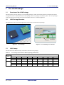
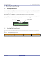
User’s Manual
LGA Mounting Manual
All information contained in these materials, including products and product specifications,
represents information on the product at the time of publication and is subject to change by
Renesas Electronics Corp. without notice. Please review the latest information published by
Renesas Electronics Corp. through various means, including the Renesas Electronics Corp.
website (http://www.renesas.com).
www.renesas.com
Rev.1.00 Mar 2014
Notice
1.
Descriptions of circuits, software and other related information in this document are provided only to illustrate the operation of
semiconductor products and application examples. You are fully responsible for the incorporation of these circuits, software, and
information in the design of your equipment. Renesas Electronics assumes no responsibility for any losses incurred by you or third
parties arising from the use of these circuits, software, or information.
2.
Renesas Electronics has used reasonable care in preparing the information included in this document, but Renesas Electronics does not
warrant that such information is error free. Renesas Electronics assumes no liability whatsoever for any damages incurred by you
resulting from errors in or omissions from the information included herein.
3.
Renesas Electronics does not assume any liability for infringement of patents, copyrights, or other intellectual property rights of third
parties by or arising from the use of Renesas Electronics products or technical information described in this document. No license,
express, implied or otherwise, is granted hereby under any patents, copyrights or other intellectual property rights of Renesas
Electronics or others.
4.
You should not alter, modify, copy, or otherwise misappropriate any Renesas Electronics product, whether in whole or in part.
Renesas Electronics assumes no responsibility for any losses incurred by you or third parties arising from such alteration, modification,
copy or otherwise misappropriation of Renesas Electronics product.
5.
Renesas Electronics products are classified according to the following two quality grades: “Standard” and “High Quality”.
recommended applications for each Renesas Electronics product depends on the product’s quality grade, as indicated below.
“Standard”:
The
Computers; office equipment; communications equipment; test and measurement equipment; audio and visual
equipment; home electronic appliances; machine tools; personal electronic equipment; and industrial robots etc.
“High Quality”: Transportation equipment (automobiles, trains, ships, etc.); traffic control systems; anti-disaster systems; anti-crime
systems; and safety equipment etc.
Renesas Electronics products are neither intended nor authorized for use in products or systems that may pose a direct threat to human
life or bodily injury (artificial life support devices or systems, surgical implantations etc.), or may cause serious property damages
(nuclear reactor control systems, military equipment etc.). You must check the quality grade of each Renesas Electronics product
before using it in a particular application. You may not use any Renesas Electronics product for any application for which it is not
intended. Renesas Electronics shall not be in any way liable for any damages or losses incurred by you or third parties arising from the
use of any Renesas Electronics product for which the product is not intended by Renesas Electronics.
6.
You should use the Renesas Electronics products described in this document within the range specified by Renesas Electronics,
especially with respect to the maximum rating, operating supply voltage range, movement power voltage range, heat radiation
characteristics, installation and other product characteristics. Renesas Electronics shall have no liability for malfunctions or damages
arising out of the use of Renesas Electronics products beyond such specified ranges.
7.
Although Renesas Electronics endeavors to improve the quality and reliability of its products, semiconductor products have specific
characteristics such as the occurrence of failure at a certain rate and malfunctions under certain use conditions. Further, Renesas
Electronics products are not subject to radiation resistance design. Please be sure to implement safety measures to guard them against
the possibility of physical injury, and injury or damage caused by fire in the event of the failure of a Renesas Electronics product, such
as safety design for hardware and software including but not limited to redundancy, fire control and malfunction prevention, appropriate
treatment for aging degradation or any other appropriate measures. Because the evaluation of microcomputer software alone is very
difficult, please evaluate the safety of the final products or systems manufactured by you.
8.
Please contact a Renesas Electronics sales office for details as to environmental matters such as the environmental compatibility of each
Renesas Electronics product. Please use Renesas Electronics products in compliance with all applicable laws and regulations that
regulate the inclusion or use of controlled substances, including without limitation, the EU RoHS Directive. Renesas Electronics
assumes no liability for damages or losses occurring as a result of your noncompliance with applicable laws and regulations.
9.
Renesas Electronics products and technology may not be used for or incorporated into any products or systems whose manufacture, use,
or sale is prohibited under any applicable domestic or foreign laws or regulations. You should not use Renesas Electronics products or
technology described in this document for any purpose relating to military applications or use by the military, including but not limited
to the development of weapons of mass destruction. When exporting the Renesas Electronics products or technology described in this
document, you should comply with the applicable export control laws and regulations and follow the procedures required by such laws
and regulations.
10. It is the responsibility of the buyer or distributor of Renesas Electronics products, who distributes, disposes of, or otherwise places the
product with a third party, to notify such third party in advance of the contents and conditions set forth in this document, Renesas
Electronics assumes no responsibility for any losses incurred by you or third parties as a result of unauthorized use of Renesas
Electronics products.
11. This document may not be reproduced or duplicated in any form, in whole or in part, without prior written consent of Renesas
Electronics.
12. Please contact a Renesas Electronics sales office if you have any questions regarding the information contained in this document or
Renesas Electronics products, or if you have any other inquiries.
(Note 1) “Renesas Electronics” as used in this document means Renesas Electronics Corporation and also includes its majority-owned
subsidiaries.
(Note 2) “Renesas Electronics product(s)” means any product developed or manufactured by or for Renesas Electronics.
(2012.4)
LGA Mounting Manual
Table of Contents
1. The LGA Package............................................................................................................................ 1
1.1
1.2
1.3
Overview of the LGA Package ................................................................................................................................. 1
LGA Package Structure ............................................................................................................................................ 1
LGA Lineup .............................................................................................................................................................. 1
2. Mounting Board Design................................................................................................................... 2
2.1
2.2
Mounting Pad Structure ............................................................................................................................................ 2
Mounting Pad Design Example ................................................................................................................................ 2
3. The Mounting Process ..................................................................................................................... 4
3.1
3.2
Details of the LGA Mounting Process ...................................................................................................................... 4
Solder Paste Printing................................................................................................................................................. 5
3.2.1
Solder Paste.................................................................................................................................................... 5
3.2.2
Stencil Examples ............................................................................................................................................ 7
3.2.3
Inspection Following Solder Printing............................................................................................................. 7
3.3
Mounting (placement)............................................................................................................................................... 8
3.3.1
Image Recognition ......................................................................................................................................... 8
3.3.2
Placement Nozzle........................................................................................................................................... 8
3.3.3
Placement Positional Error Tolerances .......................................................................................................... 9
4. The Reflow Process ....................................................................................................................... 10
4.1
Package Heat Resistance......................................................................................................................................... 10
4.1.1
Storage Conditions After Opening Moisture-Proof Packing........................................................................ 11
4.1.2
Baking Conditions........................................................................................................................................ 11
4.2
Solderability............................................................................................................................................................ 12
4.3
Post Reflow Soldered Area Inspection ................................................................................................................... 13
5. Reliability Evaluation Data............................................................................................................ 14
5.1
5.2
Impact Resistance ................................................................................................................................................... 14
Temperature Cycle Test Results ............................................................................................................................. 15
R50ZZ0006EJ0100 Rev. 1.00
Jan 22, 2014
Contents 1
LGA Mounting Manual
1. The LGA Package
1. The LGA Package
1.1
Overview of the LGA Package
The land grid array (LGA) package is a resin molding package in which the external pins have a land structure and are
arranged in a matrix on the bottom surface of the package. The LGA package is mounted by reflow. The LGA package is
widely used for microcontrollers and other semiconductor devices in consumer equipment.
1.2
LGA Package Structure
The figures below show the external appearance and structure of a Renesas LGA package.
Molded plastic
Chip
Interposer
Die attach
LGA pin
Figure 1.1 LGA Package
1.3
Figure 1.2 LGA Package Cross Section
LGA Lineup
The table below lists Renesas lineup of miniature, thin-form LGA packages.
Table 1.1
Terminal
Pitch
LGA Lineup (Pin counts for different package dimensions)
Body Size (mm)
3x3
4x4
0.65 mm
5x5
5.5x5.5
49
6x6
6.5x6.5
7x7
8x8
9x9
64
Δ81
85
113
145
100
0.50 mm
25
36
49
Δ49
64
100
113
145
177
81
Note: Cells marked with a delta (Δ) indicate which are under planning.
R50ZZ0006EJ0100 Rev. 1.00
Mar 19, 2014
Page 1 of 15
LGA Mounting Manual
2. Mounting Board Design
2. Mounting Board Design
2.1
Mounting Pad Structure
There are two types of mounting pad; solder mask defined (SMD), in which the solder resist overlays the mounting pads,
nd non solder mask defined (NSMD), in which the solder resist does not overlay the pads. While the NSMD structure is
the most common mounting pad structure, users should determine the mounting pad structure based on consideration of
the board wiring design.
The LGA land type is the NSMD type, in which the solder resist does not cover any of the land area.
The mounting pad form on the mounting board is made to be the same as that of the LGA itself, and soldering connection
geometry with a good vertical balance after reflow soldering can be achieved by designing with an NSMD structure in
which the solder resist does not cover any of the pad area.
Solder resist
Mounting pad
Mounting board
Figure 2.1 Pad Structure (NSMD structure)
2.2
Mounting Pad Design Example
This section presents a mounting pad design example for the mounting board that is matched to the LGA package land
size.
Table 2.1
Mounting Pad Design Example
(Unit: mm)
LGA land size
φ0.25
φ0.30
φ0.35
Mounting pad design
φ0.25
φ0.30
φ0.35
R50ZZ0006EJ0100 Rev. 1.00
Mar 19, 2014
Page 2 of 15
LGA Mounting Manual
2. Mounting Board Design
Mounting Pad Design Example for LGA Packages with Reinforcement Lands
Some LGA packages have the reinforcement lands which are located in the four corners. Since these reinforcement lands
increase the resistance to stress of the solder joint, we recommend designing a mounting pad that matches the
reinforcement land specifications if an LGA product that has reinforcement lands at the four corners is used.
Figure 2.2 shows a mounting pad design for a 5x5/64-pin FLGA package.
An SMD structure is used for the reinforcement pads, and an NSMD structure is used for all other pads. While the
reinforcement lands on the package have a complex shape, the form of the reinforcement pads on the mounting board is
simplified. Also, the aperture size of the metal mask used for solder printing for the reinforcement pads is set to be
roughly 80% of the SR aperture area. If an excessive amount of solder is applied to the reinforcement pad areas, a
phenomenon in which the package floats up can occur during reflow soldering due to the influence of the melted solder.
This can result in insufficient solder connections to the signal pins.
(Unit: mm)
SR aperture
Pad
Printing mask size
φ0.28 to φ0.3
φ0.24 to 0.3
C section
Line (1)
Pad diameter + 0.05 to 0.1
Mounting pad for the C section
E section
D section
Line (3)
Line (2)
0.745
Package (TopView)
0.55
0.595
Line (2)
R0.19
5
0.475
Pad
Pad for the E section
Printing mask size
About 80% of the SR
aperture area Printing
mask thickness
: 100 µm
Line (1)
0.475
0.595
SR aperture
0.55
R0.275
0.745
Line (1)
R0.12
SR aperture
Line (3)
Mounting pad for the D section
Figure 2.2 Design Example for 0.5 mm pitch 5x5/64-Pin FLGA
R50ZZ0006EJ0100 Rev. 1.00
Mar 19, 2014
Page 3 of 15
LGA Mounting Manual
3. The Mounting Process
3. The Mounting Process
3.1
Details of the LGA Mounting Process
Solder paste
(solder cream)
Lead-free solder
•
Recommended design values of stencil
Printing positional tolerances
⎯ φ0.25 mm to φ0.35 mm
0.5 mm pitch LGA: within ±0.10 mm
⎯ Thickness: 0.10 mm
0.65 mm pitch LGA: within ±0.12 mm
•
Sample solder material
⎯ M705-235C-32-11* or equivalent (M705
solder composition: Sn-3Ag-0.5Cu)
1
Placement
Precision (placement positional tolerance)
•
Placement system with recognition system
⎯ KE-760 (Juki Corporation) or equivalent
Placement positional tolerances based on
recognition of all lands or outline recognition
0.5 mm pitch LGA: within ±0.10 mm
0.65 mm pitch LGA: within ±0.12 mm
Conditions
(The same as for earlier BGA products)
0.5 mm pitch placement loading: up to 180 g
Placement speed:
39.5 mm/second to 275 mm/second
Placement push-in depth: 0 to 0.5 mm
0.65 mm pitch placement loading: 60 g to 250 g
Placement speed:
39.5 mm/second to 395 mm/second
Placement push-in depth: 0 to 2.0 mm
Reflow soldering
conditions
The reflow thermal conditions specified in the
delivery specifications document must be
followed.
•
Reflow equipment
⎯ Air reflow or nitrogen reflow equipment
(the same equipment as used for earlier
BGA products)
Notes: LGA package products can be mounted with the same conditions as BGA package, and they can also be
mounted at the same time when QFP, SOP, and similar package products are mounted.
1. Manufactured by Senju Metal Industry Co., Ltd.
The LGA mounting process is described in detail in the following pages.
R50ZZ0006EJ0100 Rev. 1.00
Mar 19, 2014
Page 4 of 15
LGA Mounting Manual
3. The Mounting Process
3.2
Solder Paste Printing
3.2.1
Solder Paste
The main components of solder paste are solder powder and flux.
(1)
Solder Powder
•
Solder powder contains a range of solder powder size as shown below, and this range affects the printability of the
solder paste.
•
The land pitch, as listed in the table below, should be taken into consideration when selecting the solder powder. Note
that solder paste with a fine particle size has issues such as the easier formation of capillary balls and degraded
wettability. This means that thorough evaluation is required during materials selection.
Source: Senju Metal Industry Co., Ltd.
Type 2
Solder powder
size range
0.075mm to 0.045mm
Type 3
0.045mm to 0.020mm
Type 4
0.038mm to 0.020mm
Type 5
0.025mm to 0.010mm
Sn-3Ag-0.5Cu
Solder powder
Figure 3.1 Electron Microscope Images of Solder Powder in Solder Paste
Table 3.1
Land Pitch and Ranges of Solder Powder Sizes in Solder Paste
Land Pitch (mm)
Solder Powder Size Range
1.27
1.00
0.80
0.65
0.50
0.40
0.075 to 0.045 mm
0.045 to 0.020 mm
0.038 to 0.020 mm
0.025 to 0.010 mm
(2)
Flux
•
There are three main types of flux: rosin based fluxes, synthetic resin fluxes, and water soluble fluxes.
•
There are three types of rosin based fluxes according to their activation level: R (rosin fluxes), RMA (mildly
activated fluxes), and RA (activated fluxes). The table below lists the features of these three types.
Table 3.2
Flux Types and Their Characteristics
Flux Type
R type, ROL type
(Non-activated Rosin, Rosin Low activity levels )
Characteristic
Non-activated fluxes, Noncorrosive.
RMA type, ROM type
Mildly activated fluxes. Noncorrosive. These fluxes have better
(Rosin Mildly Activated, Rosin Moderate activity levels) solderability than the R type fluxes.
RA type, ROH type
(Rosin Activated, Rosin High activity levels)
R50ZZ0006EJ0100 Rev. 1.00
Mar 19, 2014
Highly activated fluxes. These fluxes have better solderability
than the R and RMA type fluxes. They are, however, strongly
corrosive.
Page 5 of 15
LGA Mounting Manual
(3)
3. The Mounting Process
Characteristics Required in the Solder Paste
Printing
•
Solder powder size: A particle size of less than 1/4 to 1/5 the thickness of the stencil is most commonly selected to
assure the release characteristics in solder printing.
•
Viscosity is too high, the release characteristics of the solder can be degraded and result in thin pringing. If the
viscosity is too low, print blotting and/or print droop may occur. For printing applications, a viscosity of around 200
to 300 Pa•s/25°C is commonly used.
Before and After Reflow
•
Before reflow
⎯ Solder paste should have minimal aged deterioration during manufacturing and good printability.
⎯ Solder paste should have minimal aged deterioration after printing (it should have a long viscosity retention time
and should not cause shape collapse to occur).
⎯ The flux and the solder powder must not separate.
•
After reflow
⎯ Solder paste should have good solderability and capillary balls must not be formed.
(Note that no solder powder oxidation occurs and select a solder powder with a narrow particle size distribution.
Also, select a flux whose solvents have a low boiling point and select a solder with a high molecular weight rosin
and relatively low volume of flux itself.)
⎯ Flux residues must not affect end product reliability.
Note: The user should select the solder paste according to the application.
R50ZZ0006EJ0100 Rev. 1.00
Mar 19, 2014
Page 6 of 15
LGA Mounting Manual
3.2.2
3. The Mounting Process
Stencil Examples
The table below lists stencil design examples for various land sizes. The aperture dimensions and The thickness must be
selected by taking post reflow soldering open connections and solder bridges into account.
Table 3.3
Stencil Design Examples
φ0.25
φ0.30
φ0.35
Mounting pad design
φ0.25
φ0.30
φ0.35
Aperture diameter
φ0.25
φ0.30
φ0.35
Thickness
0.1
0.1
0.1
Stencil
3.2.3
Unit: mm
LGA land size
Inspection Following Solder Printing
The amount of solder paste has a large effect on the connection quality. In some cases, only using a 2D inspection for the
paste volume inspection will be inadequate for evaluating the post-printing print quality. We therefore recommend the
adoption of 3D inspection, especially when manufacturing high-reliability equipment.
We recommend that you consider the examples of 3D inspection equipment introduced below and examine the inspection
equipment.
Inspection photograph taken
from directly above
Inspection photograph taken
from oblique side
Low volume
3D measurement
example
Soldering evaluation
Area
2D tester
OK
Design value
Solder
Volume ICT
⎯
MK5401B
¾
NG
Source: Electronics Mounting Technology
Author: Takuo Kajima, Anritsu
Although the area is close to
the design value, the volume
is significantly below the
design value.
Figure 3.2 3D Inspection Unit Example
R50ZZ0006EJ0100 Rev. 1.00
Mar 19, 2014
Page 7 of 15
LGA Mounting Manual
3. The Mounting Process
3.3
Mounting (placement)
3.3.1
Image Recognition
When mounting devices using image recognition of lands, mounting equipment that includes land recognition software is
required. The adequate recognition ability to differentiate between signal lands (pins) and reinforcement lands, which
have a different shape and size, is necessary when performing land recognition of LGA packages that have reinforcement
lands.
All holes recognition method
All land recognition method
Fault recognized
(missing hole error)
Recognition OK
Figure 3.3 Image Recognition Result for LGA with Reinforcement Land Recognition Function
3.3.2
Placement Nozzle
Although LGA package devices have a resin molding structure, we still recommend using a suction collet that has a builtin spring to reduce the impact load applied to devices during mounting.
Placement nozzle
← Spring (to reduce mechanical shock
during placement)
LGA (suction)
Solder paste
Mounting board
Figure 3.4 Placement Nozzle Example
The optimal placement condition must be determined, following issues into consideration: the push-in amount which can
cause solder paste squashing, positional displacement, and the placement positional tolerance determined according to the
LGA package self-alignment and other issues.
R50ZZ0006EJ0100 Rev. 1.00
Mar 19, 2014
Page 8 of 15
LGA Mounting Manual
3.3.3
3. The Mounting Process
Placement Positional Error Tolerances
This section presents an example of results of self alignment evaluation for 0.5 mm pitch LGA packages.
We set the solder printing positional error and LGA placement positional error as reverse direction respectively, evaluate
and examine the tolerance.
Mounting Conditions
1. Solder paste: M705-235C-32-11 (Sn-3Ag-0.5Cu)
2. Stencil: φ0.30 mm × 0.10 mm
3. Reflow condition: 150°C to 180°C, main heating at 250°C air reflow
Solder printing positional error vs. placement positional error
(tolerances)
reinforcement lands: none
Solder paste
Top view
schematic
Solder printing
positional error (+)
LGA
Side view
schematic
Solder paste
Mounting board
Placement center
LGA placement positional error (mm)
LGA placement
positional error (-)
0.00
0.05 0.10
0.15
0.00
Self alignment region
0.20
0.25
0.30
-0.05
-0.10
-0.15
-0.20
-0.25
: NG
: OK
Placement positional error tolerance:
±0.11 mm
-0.30
Solder printing positional error (mm)
Figure 3.5 Placement Positional Error Evaluation
Figure 3.6 Placement Positional Error Evaluation Results
As a result of this evaluation, the 0.5 mm pitch LGA package placement positional error tolerances were found to be as
follows.
•
Solder paste printing positional error: ±0.10 mm
•
LGA package placement positional error: ±0.10 mm
R50ZZ0006EJ0100 Rev. 1.00
Mar 19, 2014
Page 9 of 15
LGA Mounting Manual
4. The Reflow Process
4. The Reflow Process
The reflow temperature profile must be determined based on the ability of the mounted devices to withstand heat and
their solderability.
4.1
Package Heat Resistance
To prevent adsorption of moisture after the moisture-proof packing has been opened, within the limits of the storage
condition after the opening moisture-proof packing, perform the reflow soldering operation under the following
conditions.
If time longer than the limits has elapsed, the semiconductor devices must be baked under the baking conditions shown.
Table 4.1
Component Heat Tolerance
Heat tolerance temperature: for 260°C
Maximum reflow temperature (package surface temperature)
Under 260°C
Time at temperatures over 255°C
Under 30 seconds
Time at temperatures over 217°C
60 to 150 seconds
Time at the preheat temperature of 150°C to 200°C
60 to 120 seconds
Maximum reflow temperature
(package surface temperature) (°C)
260°Cmax. Max.
255°C
217°C
200°C
150°C
30s max.
60 to 120s
60 to 150s
Time (S)
Figure 4.1 Reflow Heat Resistance Temperature Profile
•
Investigate means to assure that the heating slope is 1 to 3°C/second.
•
Set the cooling slope based on issues such as circuit board warping.
R50ZZ0006EJ0100 Rev. 1.00
Mar 19, 2014
Page 10 of 15
LGA Mounting Manual
4.1.1
Table 4.2
4. The Reflow Process
Storage Conditions After Opening Moisture-Proof Packing
Storage Conditions
Item
Conditions
Temperature
5°C to 30°C
Humidity
Under 70%RH
Time*
168 hours
4.1.2
Remarks
Note: The time from opening the moisture-proof packing until the
last reflow soldering has been completed
Baking Conditions
If the stipulated time after opening the moisture-proof packing has elapsed, the corresponding semiconductor products
should be baked. Use 10 hours at 125°C as an initial guideline.
The total baking time must not exceed 96 hours if devices are baked repeatedly.
Furthermore, if the 30% RH spot on the indicator card is pink when the moisture-proof packing is opened, the products
should be baked before mounting.
Note: The bake time is stipulated individually for each products. See the delivery specifications document for details.
R50ZZ0006EJ0100 Rev. 1.00
Mar 19, 2014
Page 11 of 15
LGA Mounting Manual
4.2
•
4. The Reflow Process
Solderability
Reflow temperature
It is important to set the temperature profile which is lower than the guaranteed heat tolerance temperature for the
mounted components. It is also important to set the temperature at the solder joint so as to exceed the lower limit
temperature which solder paste maker recommends.
If this temperature range is exceeded, solder shorting or device reliability degradation may occur, and if this
temperature range is not reached, end product quality may be reduced by failure to melt the solder or insufficient
solder joint strength.
•
Atmosphere
We recommend solder mounting in a nitrogen (N2) atmosphere, which provides improved solder wettability.
Temperature (°C)
Package heat tolerance temperature upper
limit (package surface)
Lower limit of recommended temperature for
the solder paste (for the solder joint)
Time (S)
Figure 4.2 Soldering Profile
R50ZZ0006EJ0100 Rev. 1.00
Mar 19, 2014
Page 12 of 15
LGA Mounting Manual
4.3
4. The Reflow Process
Post Reflow Soldered Area Inspection
Since the soldered section of the LGA package is the bottom surface of the package, the soldering cannot be inspected by
ordinary visual inspection. X-ray based inspection methods can therefore be effective. This section presents examples of
X-ray inspection of soldered sections.
Open circuits and solder shorts that could not be seen with visual inspection can be verified with X-ray inspection.
We recommend that the inspection results for each quality item be provided as feedback for the process management
conditions, such as the printing mask design, printing positional error allowable range, and mounting position allowable
range.
Table 4.3
Mounting Conditions
Package Type
1
Placement Force*
Placement Push-In
Reflow Temperature
180g/ic
0.20 mm
250°C
(Air Reflow)
LFLGA336-14x14-0.65
LFLGA304-13x13-0.5
Note:
1. The placement force indicates the placement nozzle spring force.
Table 4.4
Mounting Results
Metal mask thickness: 100 μm
Metal mask aperture
φ0.20 mm
LFLGA336-14x14-0.65
LFLGA304-13x13-0.5
⎯
φ0.25 mm
1
2/10*
1
6/8*
0/8
φ0.30 mm
φ0.35 mm
φ0.40 mm
φ0.45 mm
0/10
0/10
0/10
0/10
0/8
0/8
⎯
2
3/8*
Notes: 1. Solder open
2. Solder short
LFLGA336-14x14-0.65 (0.65 mm pitch)
φ0.25 mm
φ0.45 mm
φ0.20 mm
φ0.40 mm
Solder printing
After reflow
X-ray image
Solder printing positional error:
0.15 mm
Stencil
Apertures
LFLGA304-13x13-0.5 (0.5 mm pitch)
Solder short
Solder open ?
(verified by pulling away)
Solder open ?
(verified by pulling away)
Figure 4.3 X-Ray Inspection Examples
For the 0.65 mm pitch LGA package, neither opens nor shorts were found with metal mask apertures of φ0.30 to φ0.45
mm. For the 0.5 mm pitch LGA package, neither opens nor shorts were found with metal mask apertures of φ0.25 to
φ0.35 mm.
R50ZZ0006EJ0100 Rev. 1.00
Mar 19, 2014
Page 13 of 15
LGA Mounting Manual
5. Reliability Evaluation Data
5. Reliability Evaluation Data
5.1
Impact Resistance
This section presents the evaluation results of impact resistance for LGA which is mounted on the board. The evaluation
is impact bending test which is stipulated in JEITA ED-4702B, and high speed deformation is applied to the board.
This result showed that even LGA packages without reinforcement lands are resistant to ordinary impacts (1500 με).
This result also showed that LGA packages with reinforcement lands have relatively better resistance to impacts, and that
the use of LGA packages with reinforcement lands is preferable for equipment that requires increased impact resistance.
Table 5.1
Impact Bending Test Results
Reinforcement
Lands
Solder paste: M705-235C-32-11 (Sn-3Ag-0.5Cu)
Reflow conditions: Preheating at 150°C to 180°C for 90 seconds + main heating at 250°C
Solder Mask
Mounting Board Deformation
2000 με
3000 με
5000 με
φ0.25 mm
Present
φ0.30 mm
φ0.35 mm
φ0.25 mm
None
φ0.30 mm
φ0.35 mm
: Pass
: Open
Reinforcement lands present *1
No reinforcement lands
φ0.25 mm × 0.10 mmt
Drop rod
Mounting
board
φ0.30 mm × 0.10 mmt
Package
Fixed span
φ0.35 mm × 0.10 mmt
Board deformation (ppm)
Impact bending test method
(JEITA ED-4702B)
Apply impact
2000
1000
0
-1000
0
0.005
0.010
Time (s)
Board strain
waveform example
Note: 1. Reinforcement land solder mask: 0.9 mm square × 0.10 mm thickness
Figure 5.1 Impact Bending Test Inspection Result and Test Method
R50ZZ0006EJ0100 Rev. 1.00
Mar 19, 2014
Page 14 of 15
LGA Mounting Manual
5.2
5. Reliability Evaluation Data
Temperature Cycle Test Results
This section presents an example of temperature cycle test results for LGA package types mounted with a lead-free solder
paste (SAC305: Sn-3Ag-0.5Cu).
Although single-sided mounting provided superior results, fully adequate temperature cycle characteristics were achieved
even by double sided mounting that assumes the use of high-density mounting equipment.
Table 5.2
Temperature Cycle Test Results Comparison
Size
Land pitch
Reinforcement
lands
Present
Mounting type
Single sided
Sample 1
Sample 2
Sample 3
5 × 5 mm
5 × 5 mm
5 × 5 mm
0.5 mm
0.5 mm
0.65 mm
SAC305
SAC305
SAC305
None
Double sided
Solder paste
Mounting board
FR4/4 layers
FR4/4 layers
FR4/4 layers
Test conditions
−40°C to 125°C
−25°C to 125°C
−25°C to 125°C
3086 cyc
1870 cyc
2111 cyc
1%TTF
R50ZZ0006EJ0100 Rev. 1.00
Mar 19, 2014
Page 15 of 15
LGA Mounting Manual
Publication Date:
Rev.1.00
Mar 19, 2014
Published by:
Renesas Electronics Corporation
http://www.renesas.com
SALES OFFICES
Refer to "http://www.renesas.com/" for the latest and detailed information.
Renesas Electronics America Inc.
2801 Scott Boulevard Santa Clara, CA 95050-2549, U.S.A.
Tel: +1-408-588-6000, Fax: +1-408-588-6130
Renesas Electronics Canada Limited
1101 Nicholson Road, Newmarket, Ontario L3Y 9C3, Canada
Tel: +1-905-898-5441, Fax: +1-905-898-3220
Renesas Electronics Europe Limited
Dukes Meadow, Millboard Road, Bourne End, Buckinghamshire, SL8 5FH, U.K
Tel: +44-1628-585-100, Fax: +44-1628-585-900
Renesas Electronics Europe GmbH
Arcadiastrasse 10, 40472 Düsseldorf, Germany
Tel: +49-211-6503-0, Fax: +49-211-6503-1327
Renesas Electronics (China) Co., Ltd.
Room 1709, Quantum Plaza, No.27 ZhiChunLu Haidian District, Beijing 100191, P.R.China
Tel: +86-10-8235-1155, Fax: +86-10-8235-7679
Renesas Electronics (Shanghai) Co., Ltd.
Unit 301, Tower A, Central Towers, 555 Langao Road, Putuo District, Shanghai, P. R. China 200333
Tel: +86-21-2226-0888, Fax: +86-21-2226-0999
Renesas Electronics Hong Kong Limited
Unit 1601-1613, 16/F., Tower 2, Grand Century Place, 193 Prince Edward Road West, Mongkok, Kowloon, Hong Kong
Tel: +852-2265-6688, Fax: +852 2886-9022/9044
Renesas Electronics Taiwan Co., Ltd.
13F, No. 363, Fu Shing North Road, Taipei 10543, Taiwan
Tel: +886-2-8175-9600, Fax: +886 2-8175-9670
Renesas Electronics Singapore Pte. Ltd.
80 Bendemeer Road, Unit #06-02 Hyflux Innovation Centre, Singapore 339949
Tel: +65-6213-0200, Fax: +65-6213-0300
Renesas Electronics Malaysia Sdn.Bhd.
Unit 906, Block B, Menara Amcorp, Amcorp Trade Centre, No. 18, Jln Persiaran Barat, 46050 Petaling Jaya, Selangor Darul Ehsan, Malaysia
Tel: +60-3-7955-9390, Fax: +60-3-7955-9510
Renesas Electronics Korea Co., Ltd.
12F., 234 Teheran-ro, Gangnam-Ku, Seoul, 135-920, Korea
Tel: +82-2-558-3737, Fax: +82-2-558-5141
© 2014 Renesas Electronics Corporation. All rights reserved.
Colophon 3.0
LGA Mounting Manual
R50ZZ0006EJ0100