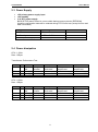
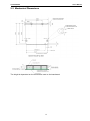
1
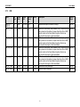
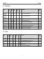
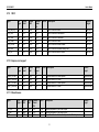
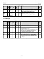
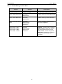
Q7-US15W-FD MSC Qseven™ Module Rev. 0.91 March 21th, 2011 User’s Manual Q7-US15W-FD Preface Copyright Notice Copyright © 2008 MSC Vertriebs GmbH. All rights reserved. Copying of this document, and giving it to others and the use or communication of the contents thereof, is forbidden without express authority. Offenders are liable to the payment of damages. All rights are reserved in the event of the grant of a patent or the registration of a utility model or design. Important Information This documentation is intended for qualified audience only. The product described herein is not an end user product. It was developed and manufactured for further processing by trained personnel. Disclaimer Although this document has been generated with the utmost care no warranty or liability for correctness or suitability for any particular purpose is implied. The information in this document is provided “as is” and is subject to change without notice. EMC Rules This unit has to be installed in a shielded housing. If not installed in a properly shielded enclosure, and used in accordance with the instruction manual, this product may cause radio interference in which case the user may be required to take adequate measures at his or her owns expense. Trademarks All used product names, logos or trademarks are property of their respective owners. Certification MSC Vertriebs GmbH is certified according to DIN EN ISO 9001:2000 standards. Life-Cycle-Management MSC products are developed and manufactured according to high quality standards. Our lifecycle-management assures long term availability through permanent product maintenance. Technically necessary changes and improvements are introduced if applicable. A productchange-notification and end-of-life management process assures early information of our customers. Product Support MSC engineers and technicians are committed to provide support to our customers whenever needed. Before contacting Technical Support of MSC Vertriebs GmbH, please consult the respective pages on our web site at www.msc-ge.com/support-boards for the latest documentation, drivers and software downloads. If the information provided there does not solve your problem, please contact our Technical Support: Email: [email protected] Phone: +49 8165 906-200 2 User’s Manual Q7-US15W-FD Content 1. 2 3 4 5 General Information ............................................................................................................................ 5 1.1 Revision History .......................................................................................................................... 5 1.2 Reference Documents ................................................................................................................ 5 1.3 Introduction.................................................................................................................................. 6 Technical Description ......................................................................................................................... 7 2.1 Key features ................................................................................................................................ 7 2.1.1 Ordering information ............................................................................................................... 9 2.2 Block diagram ........................................................................................................................... 10 2.3 Power Supply ............................................................................................................................ 11 2.4 Power dissipation ...................................................................................................................... 11 2.5 Mechanical Dimensions ............................................................................................................ 12 2.6 Thermal specifications .............................................................................................................. 13 2.7 Signal description ...................................................................................................................... 14 2.7.1 High Definition Audio ............................................................................................................ 14 2.7.2 Ethernet ................................................................................................................................ 14 2.7.3 Serial ATA ............................................................................................................................. 15 2.7.4 PCI Express Lanes ............................................................................................................... 15 2.7.5 USB ....................................................................................................................................... 16 2.7.6 LVDS Flat Panel ................................................................................................................... 17 2.7.7 LPC Bus ................................................................................................................................ 17 2.7.8 SDVO .................................................................................................................................... 18 2.7.9 SDIO ..................................................................................................................................... 19 2.7.10 Express card support ............................................................................................................ 19 2.7.11 Miscellaneous ....................................................................................................................... 19 2.7.12 Power and System Management.......................................................................................... 20 2.7.13 Power and GND .................................................................................................................... 21 2.8 Connectors ................................................................................................................................ 22 2.8.1 Module connector ................................................................................................................. 22 Jumpers ............................................................................................................................................. 26 3.1 Crisis recovery jumper .............................................................................................................. 26 3.2 Clear CMOS jumper .................................................................................................................. 27 System resources ............................................................................................................................. 28 4.1 SMB Address Map .................................................................................................................... 28 4.2 PCI Express Lanes ................................................................................................................... 28 4.3 USB ........................................................................................................................................... 28 4.4 PCI Devices............................................................................................................................... 29 BIOS .................................................................................................................................................... 30 5.1 Introduction................................................................................................................................ 30 5.1.1 Startup Screen Overview ...................................................................................................... 30 5.1.2 Activity Detection Background .............................................................................................. 30 5.2 TrustedCore Setup Utility .......................................................................................................... 31 5.2.1 Configuring the System BIOS ............................................................................................... 31 5.2.2 The Main Menu ..................................................................................................................... 33 5.2.3 The Advanced Menu ............................................................................................................. 35 5.2.4 The Power Menu .................................................................................................................. 46 5.2.5 The Boot Menu ..................................................................................................................... 47 5.2.6 The Exit Menu ....................................................................................................................... 48 5.3 BIOS and Firmware Update ...................................................................................................... 49 3 User’s Manual Q7-US15W-FD 5.4 Bios Crisis Recovery ................................................................................................................. 50 5.5 Diagnostics Postcodes .............................................................................................................. 53 5.5.1 Bootblock Bios Postcodes .................................................................................................... 53 5.5.2 System Bios Postcodes ........................................................................................................ 54 5.5.3 Memory Detection Postcodes ............................................................................................... 57 5.5.4 ACPI Postcodes .................................................................................................................... 58 4 User’s Manual Q7-US15W-FD 1. General Information 1.1 Revision History Rev. 0.1 Date Initial version, based on MSC_Q7-US15W_User_Manual.doc th Minor changes th Bios part updated according to Bios V2.00. Added PCI IRQ routing table. Jan 18 2010 0.2 Jan 18 2010 0.3 Feb 26 ,2010 0.4 Mar 2 0.5 0.6 0.7 0.8 Description th nd 2010 th Mar 12 2010 rd July 23 2010 rd August 3 2010 Minor corrections SSD Modell Number added Updated Bios chapter Minor corrections st Layout changes, minor corrections th September 1 2010 0.9 September 7 2010 Formatting 0.91 March 21th 2011 Block Diagram change chapter 2.2 (changed EDID EEPROM to SPD EEPROM) 1.2 Reference Documents [1] Qseven Specification Revision 1.11 th Last update: Nov. 26 2008 [2] PCI Local Bus Specification Rev. 2.1 PCI21.PDF st Last update: June 1 , 1995 http://www.pcisig.com [3] Serial ATA Specification Serial ATA 1.0 gold.pdf th Last update: August 29 , 2002 Rev.1.0 http://www.sata-io.org/ [4] IEEE Std. 802.3-2002 802.3-2002.pdf http://www.ieee.org [5] Universal Bus Specification usb_20.pdf th Last update: April 27 , 2000 http://www.usb.org 5 User’s Manual Q7-US15W-FD 1.3 Introduction Qseven modules are compact, highly integrated Single Board Computers. Typically a Qseven module consists of CPU, chipset, memory, Ethernet controller, BIOS flash, SATA- and USB controller. Interface controllers (e.g. for PCMCIA) or connectors (e.g. RJ45) are implemented on a base board on to which the Qseven module can be mounted. In addition to the power supply PCIe, SATA, USB, LPC etc. interfaces are present on the connector. Thanks to the standardized mechanics and interfaces the system can be scaled arbitrarily. Despite the modular concept the system design is very flat and compact. Qseven modules require a base board to build a working system. For evaluation purposes MSC recommends the official Qseven Reference Platform MSC Q7-MB-RP. 6 User’s Manual Q7-US15W-FD 2 Technical Description 2.1 Key features Core: Processors: Intel Atom Z510 (1.1 GHz) or Intel Atom Z530 (1.6 GHz) Chipset: Intel US15W Memory: DDR2 400/533Mhz, soldered on module 512MB or 1GB PCI Express Interface: One PCIe x1 channel Video: Chipset integrated Graphics Media Accelerator 500 18-24 bpp single channel LVDS 1x SDVO Ethernet: 1x 10/100/1000 Base –T LAN Audio: High-Definition Audio USB: 8x USB Ports (6x USB 1.1/2.0, 2x USB 2.0 only ports, optional 1x USB Client) I2C Bus 100kHz speed only. SMBus LPC Bus SATA/PATA SSD 1x SATA port Optional 1xPATA SSD with 4GB Memory SST85LP1004A 7 User’s Manual Q7-US15W-FD SDIO: 8 bit SDIO port (SDIO1.1 supported using 4 bit protocol) BIOS: Phoenix SecureCore BIOS with optional TPM support. Supports FWH on base board or on module. EEPROM: A SMBus EEPROM is implemented for backup of the CMOS data including user BIOS setup. Realtime Clock: A RTC (integrated in US15W chipset) is available. Watchdog Watchdog with programmable time-out Watchdog enabled via BIOS or application programs System Monitoring: Monitored values: Temperatures (CPU and Board) CPU and system fan speed Fan support: Optional connector on module to run active cooling fan or system fan. Speed control via monitoring device. TPM: Optional Infineon TPM 1.2 8 User’s Manual Q7-US15W-FD 2.1.1 Ordering information Ordering number Part name 32456 Q7-US15W-001 32457 Q7-US15W-002 32128 Q7-US15W-003 32458 Q7-US15W-004 *) Solid State Disk SSD85LP1004A CPU Z510 Z530 Z510 Z530 9 SSD NO NO 4GB*) 4GB*) TPM NO NO YES YES Memory 512MB 1GB 1GB 1GB User’s Manual Q7-US15W-FD 2.2 Block diagram Qseven Connector Qseven Connector JTAG/BSL XDP-SFF CPU TEMP CPU ATOM Z5x0 FSB MANUFACTORING PINS JTAG/BSL IMVP-6+ 400/533MHz DDR2 Channel US15W System Control Hub HD-AUDIO On Board Memory 1GByte/512MByte 400/533MHz SDIO/MMC HDA-Link SDVO CLOCK CK610 PCIe 1 SDVO PCIE0 SSD PATA/SATA Converter Sata 0 PATA USB USB 0...7 LVDS LVDS LPC LPC SMB TPM FWH SST49LF008A Gigabit Ethernet 82583V PCIe 2 GPIO GIGABIT LAN SMBUS SMBUS PWR-SEQ SPD EEPROM SMBus EEPROM AT24C02 Communication AT24C04 Power Sequencing I2C_Q7 I2C µC control signals Powersequencing I2C FAN1 FAN1 I2C_INT HW Monitor W83L771AWG Voltage Regulators CPU TEMP control signals Config EEPROM AT24C04 MSC-Q7-US15W-FD SSD Flash depends on the Module type used. 10 FAN1 User’s Manual Q7-US15W-FD 2.3 Power Supply +5V primary power supply input +5V standby 3.3V RTC power supply BIOS SETUP data is stored in a non volatile backup memory device (EEPROM), therefore configuration data will be retained during RTC-Power loss (except for time and date information) Voltage Input range Current +5V +4.75V - 5.25V See next table +5V Standby +4.75V - 5.25 V +3V RTC power supply +2.0V - 3.3V ca. 4uA/ max 6uA 2.4 Power dissipation CPU: 1.1GHz Ram: 1GByte Testsoftware: Performance Test Idle Calculation Memory Find prime Number Block read Idle DOS Windows S0 S3 3,6W 3,2W 0,5W 4,1W Graphic 2D Graphic complex test 3,6W Graphic 3D Graphic complex test 4,5W 4,5W CPU: 1.6GHz Ram: 1GByte Idle Calculation Memory Find prime number Block read Idle DOS Windows S0 S3 7,2W 4,8W 0,5W 5,3W 5,6W 11 Graphic 2D Graphic complex test Graphic 3D Graphic complex test 6W 6,6W User’s Manual Q7-US15W-FD 2.5 Mechanical Dimensions The height is dependent on the connectors used on the baseboard. 12 User’s Manual Q7-US15W-FD 2.6 Thermal specifications The cooling solution for a QSeven module is based on a heatspreader concept. A heatspreader is a metal plate (typically aluminium) mounted on top of the module. The connection between this plate and the module components is typically made using thermal interface materials such as phase change foils, gap pads and copper or aluminium blocks. A very good thermal conductivity is required in order to transfer the heat from the cpu and the chipset to the heatspreader plate. The heatspreader used by the MSC module is thermally attached using phase change materials and small aluminium blocks filling the gap between cpu and chipset dies and heatspreader plate. The heatspreader is not a heatsink! It is a defined thermal interface for the system designer with fixed mechanical dimensions, so it should be possible to use different module types without problem. There must be a cooling solution for the system, the surface temperature of the heatspreader should not exceed 60°C The main goal for the thermal design of a system is that each device on the module is operated within its specified thermal limits. The max temperature of CPU and chipset are 90°C, so there may be system implementations where the heatspreader temperature could be higher.In such a case the cooling solution design should be validated such that the thermal specifications of all the components on the module are not violated across the system operating temperature range even under worst case conditions. 13 User’s Manual Q7-US15W-FD 2.7 Signal description In the following tables signals are marked with the power rail associated with the pin, and, for input and I/O pins, with the input voltage tolerance. The pin power rail and the pin input voltage tolerance may be different. An additional label, “Suspend”, indicates that the pin is active during suspend states (S3, S4, S5). If suspend modes are used, then care must be taken to avoid loading signals that are active during suspend to avoid excessive suspend mode current draw. 2.7.1 High Definition Audio Signal HDA_RST# HDA_SYNC HDA_CLK HDA_SDO Pin Type Output Output Output Output Signal Level CMOS CMOS CMOS CMOS Power Rail Core Core Core Core Power Tolerance 3.3V 3.3V 3.3V 3.3V HDA_SDI Input CMOS Core 3.3V 2.7.2 PU/PD Description Source / Target Reset output to CODEC, active low. US15W 48kHz fixed-rate, sample-synchronization signal to the CODEC(s). US15W 24.00 MHz serial data clock US15W Serial TDM data output to the CODEC. US15W Serial TDM data inputs from up to 3 CODECs. US15W Ethernet Signal GBE0_MDI[0:3]+ GBE0_MDI[0:3]- GBE0_ACT# GBE0_LINK# Pin Signal Type Level Input/ Analog Output Open Drain Open Drain Power Rail 3.3V Sus Power PU/PD Description Tolerance Gigabit Ethernet Controller 0: Media Dependent Interface Differential Pairs 0,1,2,3. The MDI can operate in 1000, 100 and 10 Mbit / sec modes. CMOS 3.3V Sus 3.3V MDI[0]+/B1_DA+/MDI[1]+/B1_DB+/MDI[2]+/B1_DC+/MDI[3]+/B1_DD+/Gigabit Ethernet Controller 0 activity indicator, active low. CMOS 3.3V Sus 3.3V Gigabit Ethernet Controller 0 link indicator, active low. 14 Source / Target 82574 Microcontroller Microcontroller User’s Manual Q7-US15W-FD Signal Pin Type GBE0_LINK100# Open Drain GBE0_LINK1000# Open Drain GBE0_CTREF REF 2.7.3 Signal Level CMOS Power Rail 3.3V Sus CMOS 3.3V Sus Power PU/PD Description Tolerance 3.3V Gigabit Ethernet Controller 0 100 Mbit / sec link indicator, active low. 3.3V Gigabit Ethernet Controller 0 1000 Mbit / sec link indicator, active low. GND min 82574 (1000MBit) : 1,9V 3.3V max Source / Target Microcontroller Microcontroller 82574 Serial ATA Signal Pin Type O Signal Level SATA Power Rail 3.3V SATA0_RX+ SATA0_RX- I SATA 3.3V SATA_ACT# O CMOS 3.3V SATA0_TX+ SATA0_TX- 2.7.4 PCI Express Lanes Signal Pin Type Signal Level Power Rail PCIE_TX[0]+ PCIE_TX[0]- O PCIe Core PCIE_RX[0]+ PCIE_RX[0]- I PCIe Core Remark AC coupled on module AC coupled on module 3.3V PU/PD Description Serial ATA Channel 0 transmit differential pair. Source / Target JMH330 Serial ATA Channel 0 receive differential pair. JMH330 SATA activity indicator, active low. JMH330 Remark / PU/PD Description Power Tol. AC PCI Express Differential Transmit Pairs 0 coupled on module AC PCI Express Differential Receive Pairs 0 coupled off module 15 Source / Target US15W US15W User’s Manual Q7-US15W-FD 2.7.5 USB Signal Pin Type USB[0:7]+ I/O USB[0:7]USB_0_1_OC# I USB Remark / Power Tol. 3.3V Sus 3.3V CMOS 3.3V Sus 3.3V 10k PU USB_2_3_OC# I CMOS 3.3V Sus 3.3V 10k PU USB_4_5_OC# I CMOS 3.3V Sus 3.3V 10k PU USB_6_7_OC# I CMOS 3.3V Sus 3.3V 10k PU USB_CL_PRES I CMOS 3.3V Sus 3.3V 10k PU USB over-current sense, USB channels 0 and 1. A pull-up for this line is present on the module. An open drain driver from a USB current monitor on the Carrier Board may drive this line low. Do not pull this line high on the Carrier Board. USB over-current sense, USB channels 2 and 3. A pull-up for this line is present on the module. An open drain driver from a USB current monitor on the Carrier Board may drive this line low. Do not pull this line high on the Carrier Board. USB over-current sense, USB channels 4 and 5. A pull-up for this line is present on the module. An open drain driver from a USB current monitor on the Carrier Board may drive this line low. Do not pull this line high on the Carrier Board. USB over-current sense, USB channels 6 and 7. A pull-up for this line is present on the module. An open drain driver from a USB current monitor on the Carrier Board may drive this line low. Do not pull this line high on the Carrier Board. USB external Host present pin USB_HC_SEL CMOS 3.3V Sus 3.3V 100k PD USB Host control select pin I Signal Level Power Rail PU/PD Description Source / Target USB differential pairs, channels 0 through 7 US15W US15W US15W 16 US15W US15W US15W US15W User’s Manual Q7-US15W-FD 2.7.6 LVDS Flat Panel Signal Pin Type Signal Level Power Rail LVDS_A[0:3]+ LVDS_A[0:3]LVDS_A_CK+ LVDS_A_CKLVDS_PPEN O LVDS O LVDS_BLEN Description Source / Target Core LVDS Channel A differential pairs US15W LVDS Core LVDS Channel A differential clock US15W O CMOS Core 3.3V LVDS panel power enable US15W O CMOS Core 3.3V LVDS panel backlight enable US15W LVDS_BKLT_CTRL O CMOS Core 3.3V LVDS panel backlight brightness control US15W LVDS_BLC_CLK LVDS_BLC_DAT LVDS_DID_CLK I/O OD I/O OD I/O OD CMOS CMOS CMOS 3.3V 3.3V 3.3V 3.3V 3.3V 3.3V 10k PU 10k PU 10k PU I2C clock output for external SSC clock chip use I2C data line for external SSC clock chip use I2C clock output for LVDS display use US15W US15W US15W LVDS_DID_DAT I/O OD CMOS 3.3V 3.3V 10k PU I2C data line for LVDS display use US15W 2.7.7 Remark / Power Tol. PU/PD LPC Bus Signal Pin Type Signal Level Power Rail PU/PD Description Source / Target Core Remark / Power Tol. 3.3V LPC_AD[0:3] I/O CMOS 20k PU LPC multiplexed address, command and data bus US15W LPC_FRAME# LPC_LDRQ# O I CMOS CMOS Core Core 3.3V 3.3V LPC frame indicates the start of an LPC cycle 10k PU LPC serial DMA request, not supported US15W US15W SERIRQ I/O CMOS Core 3.3V 10k PU LPC serial interrupt US15W LPC_CLK O CMOS 3.3V 3.3V LPC clock output - 33MHz nominal 17 US15W User’s Manual Q7-US15W-FD 2.7.8 SDVO Signal Pin Type Signal Level SDVO_RED+ SDVO_RED- O PCIe SDVO_GREEN+ SDVO_GREEN- O PCIe SDVO_BLUE+ SDVO_BLUE- O PCIe SDVO_BCLK+ SDVO_BCLK- O PCIe SDVO_INT+ SDVO_INT- I PCIe SDVO_TVCLKIN+ SDVO_TVCLKIN- I PCIe SDVO_FLDSTALL+ I SDVO_FLDSTALL- PCIe SDVO_CTRL_CLK I/O OD CMOS SDVO_CTRL_DAT I/O OD CMOS Power Rail Description Source / Target Serial Digital Video red output differential pair US15W Serial Digital Video green output differential pair US15W Serial Digital Video blue output differential pair US15W Serial Digital Video clock output differential pair. US15W Serial Digital Video interrupt input differential pair. US15W Serial Digital Video TVOUT synchronization clock input differential pair, not supported US15W Serial Digital Video Field Stall input differential pair, not supported US15W Core Remark / PU/PD Power Tol. AC coupled on module AC coupled on module AC coupled on module AC coupled on module AC coupled off module AC coupled off module AC coupled off module 3.3V 1M PU SDVO I2C clock line - to set up SDVO peripherals. US15W Core 3.3V SDVO I2C data line - to set up SDVO peripherals. US15W 1M PU 18 User’s Manual Q7-US15W-FD 2.7.9 SDIO Signal Pin Type Signal Level Power Rail SDIO_DAT[0:7] I/O 3.3V Core Remark / Power Tol. 3.3V PU/PD Description Source / Target SDIO Controller Data US15W SDIO_CD# I 3.3V Core 3.3V SDIO Controller Card Detect US15W SDIO_CMD SDIO_CLK# I/O O 3.3V 3.3V Core Core 3.3V 3.3V SDIO_PWR# I/O 3.3V Core 3.3V SDIO Controller Power enable US15W SDIO_LED O 3.3V Core 3.3V SDIO Controller transfer activity LED US15W SDIO_WP I 3.3V Core 3.3V SDIO Controller Write Protect US15W Signal Level Power Rail EXCD0_CPPE# I EXCD0_PERST# O 3.3V 3.3V Core Core Remark / Power Tol. 3.3V 3.3V EXCD1_CPPE# I EXCD1_PERST# O 3.3V 3.3V Core Core 3.3V 3.3V 10k PU SDIO Controller Command SDIO Controller Clock US15W US15W 2.7.10 Express card support Signal Pin Type PU/PD Description Source / Target Express card slot 0 card request Express card slot 0 reset Microcontroller Microcontroller Express card slot 1 card request Express card slot 1 reset Microcontroller Microcontroller 2.7.11 Miscellaneous Signal Pin Type Signal Level I2C_CLK I2C_DAT SPKR I/O I/O O CMOS CMOS CMOS Power Remark / PU/PD Rail Power Tol. 3.3V 3.3V 2k PU 3.3V 3.3V 2k PU 3.3V 3.3V Description General purpose I2C port clock output General purpose I2C port data I/O line Output for audio enunciator - the "speaker" in PC-AT systems 19 Source / Target User’s Manual Q7-US15W-FD Signal Pin Type Signal Level BIOS_DISABLE# I WDOUT O CMOS CMOS Power Remark / PU/PD Rail Power Tol. 3.3V 3.3V 10k PU 3.3V 3.3V WDTRIG# I CMOS 3.3V FAN_TACHOIN FAN_PWMOUT I O CMOS CMOS 3.3V 3.3V 3.3V 10k PU Description Source / Target Module BIOS disable input. Pull low to disable module BIOS. Output indicating that a watchdog time-out event has occurred. Microcontroller Watchdog trigger input. This signal restarts the watchdog timer Microcontroller Tachometer input Pulse width modulation output for fan speed control Microcontroller Microcontroller 2.7.12 Power and System Management Signal Pin Type Signal Level Power Rail PWRBTN# RSTBTN# I I CMOS CMOS Remark / Power Tol. 3.3V Sus 3.3V 3.3V Sus 3.3V SUS_STAT# SUS_S3# SUS_S5# O O O CMOS CMOS CMOS 3.3V Sus 3.3V 3.3V Sus 3.3V 3.3V Sus 3.3V WAKE# BATLOW# THRM# I I I CMOS CMOS CMOS 3.3V Sus 3.3V 3.3V Sus 3.3V 3.3V 3.3V THERMTRIP# O CMOS 3.3V SMB_CLK SMB_DAT SMB_Alert SLP_BTN# I/O I/O I/O I CMOS CMOS CMOS CMOS PU/PD Description 10k PU 10k PU Power button to bring system into a power state. (Negative pulse) Reset button input. Active low input. System is held in hardware reset while this input is low, and comes out of reset upon release. (Negative pulse) Indicates low power suspend operation Indicates system is in Suspend to RAM state. Active low output. Indicates system is in Soft Off state. Also known as "PS_ON" and can be used to control an ATX power supply. External system wake up signal. Indicates that external battery is low. Input from off-module temp sensor indicating an over-temp situation. Active low output indicating that the CPU has entered thermal shutdown. System management clock line System management data line System management bus alert input Sleep button. Low active signal to bring the system in sleep state. (Negative pulse) 10k PU 10k PU 8k2 PU 3.3V 3.3V 3.3V 3.3V 3.3V Sus 2k PU 2k PU 10k 10k PU 20 Source / Target User’s Manual Q7-US15W-FD Signal Pin Type Signal Level LID_BTN# I CMOS BATLOW# PWGIN I I CMOS Low<0.6V High>0.8V Power Rail Remark / Power Tol. 3.3V Sus 3.3V Sus 5V PU/PD Description Source / Target 10k PU LID button. Low active signal detect a LID switch to bring the system in sleep state or wake up again.(Low signal) 10k PU Battery low input indicates a external battery low state 120k PD Indicates that the external power supply is ready 2.7.13 Power and GND Signal Pin Type Signal Level Power Rail VCC_5V Power 5V (±5%) VCC_5V_SBY Power 5V (±5%) VCC_RTC GND Power Power Remark / Power Tol. PU/PD Description Primary power input: +5V (±5%) Source / Target Voltage Regulators Standby power input: +5.0V (±5%) VCC3.3V All available VCC_5V_SBY pins on the connector(s) shall be used. SUS Used for microcontroller and standby and suspend functions. regulator If no standby power is available connect to VCC_5V Real-time clock circuit-power input : +3.0V (+2.0V to +3.3V) Ground - DC power and signal and AC signal return path. All available GND connector pins shall be used and tied to Carrier Board GND plane. 21 User’s Manual Q7-US15W-FD 2.8 Connectors Qseven™ Module Edge Connector 2.8.1 Module connector Row A 1 3 5 7 9 11 13 15 17 19 21 23 KEY 25 27 29 31 33 35 37 39 41 Row B 2 4 6 8 10 12 14 16 18 20 22 24 KEY 26 28 30 32 34 36 38 40 42 GND GBE_MDI3GBE_MDI3+ GBE_LINK100# GBE_MDI1GBE_MDI1+ GBE_LINK# GBE_CTREF WAKE# SUS_STAT# SLP_BTN# GND GND BATLOW# SATA0_TX+ SATA0_TXSATA_ACT# SATA0_RX+ SATA0_RXGND BIOS_DISABLE# 22 GND GBE_MDI2GBE_MDI2+ GBE_LINK1000# GBE_MDI0GBE_MDI0+ GBE_ACT# SUS_S5# SUS_S3# PWRBTN# LID_BTN# GND PWGIN RSTBTN# SATA1_TX+ SATA1_TXGND SATA1_RX+ SATA1_RXGND SDIO_CLK# User’s Manual Q7-US15W-FD 43 45 47 49 51 53 55 57 59 61 63 65 67 69 71 73 75 77 79 81 83 85 87 89 91 93 95 97 99 101 103 105 107 109 111 113 115 117 119 121 123 125 127 129 SDIO_CD# SDIO_CMD SDIO_PWR# SDIO_DAT0 SDIO_DAT2 SDIO_DAT4 SDIO_DAT6 GND HDA_SYNC HDA_RST# HDA_BITCLK HDA_SDI HDA_SDO THRM# THRMTRIP# GND USB_P7USB_P7+ USB_6_7_OC# USB_P5USB_P5+ USB_2_3_OC# USB_P3USB_P3+ USB_CL_PRES USB_P1USB_P1+ GND LVDS_A0+ LVDS_A0LVDS_A1+ LVDS_A1LVDS_A2+ LVDS_A2LVDS_PPEN LVDS_A3+ LVDS_A3GND LVDS_A_CLK+ LVDS_A_CLKLVDS_BLT_CTRL LVDS_DID_DAT LVDS_DID_CLK RSVD 44 46 48 50 52 54 56 58 60 62 64 66 68 70 72 74 76 78 80 82 84 86 88 90 92 94 96 98 100 102 104 106 108 110 112 114 116 118 120 122 124 126 128 130 23 SDIO_LED SDIO_WP SDIO_DAT1 SDIO_DAT3 SDIO_DAT5 SDIO_DAT7 NC GND SMB_CLK SMB_DAT SMB_ALERT# I2C_CLK I2C_DAT WDTRIG# WDOUT GND USB_P6USB_P6+ USB_4_5_OC# USB_P4USB_P4+ USB_0_1_OC# USB_P2USB_P2+ USB_HC_SEL USB_P0USB_P0+ GND NC NC NC NC NC NC LVDS_BLEN NC NC GND NC NC RSVD LVDS_BLC_DAT LVDS_BLC_CLK RSVD User’s Manual Q7-US15W-FD 131 133 135 137 139 141 143 145 147 149 151 153 155 157 159 161 163 165 167 169 171 173 175 177 179 181 183 185 187 189 191 193 195 197 199 201 203 205 207 209 211 213 215 217 SDVO_BCLK+ SDVO_BCLKGND SDVO_GREEN+ SDVO_GREENGND SDVO_BLUE+ SDVO_BLUEGND SDVO_RED+ SDVO_REDNC PCIE_CLK_REF+ PCIE_CLK_REFGND PCIE3_TX+ PCIE3_TXGND PCIE2_TX+ PCIE2_TXEXCD0_PERST# PCIE1_TX+ PCIE1_TXEXCD0_CPPE# PCIE0_TX+ PCIE0_TXGND LPC_AD0 LPC_AD2 LPC_CLK SERIRQ VCC_RTC FAN_TACHOIN GND RSVD RSVD RSVD VCC_5V_SB MFG_NC0 MFG_NC1 VCC VCC VCC VCC 132 134 136 138 140 142 144 146 148 150 152 154 156 158 160 162 164 166 168 170 172 174 176 178 180 182 184 186 188 190 192 194 196 198 200 202 204 206 208 210 212 214 216 218 24 SDVO_INT+ SDVO_INTGND SDVO_FLDSTALL+ SDVO_FLDSTALLGND SDVO_TVCLKIN+ SDVO_TVCLKINGND SDVO_CTRL_DAT SDVO_CTRL_CLK NC PCIE_WAKE# PCIE_RST# GND PCIE3_RX+ PCIE3_RXGND PCIE2_RX+ PCIE2_RXEXCD1_PERST# PCIE1_RX+ PCIE1_RXEXCD1_CPPE# PCIE0_RX+ PCIE0_RXGND LPC_AD1 LPC_AD3 LPC_FRAME# LPC_LDRQ# SPKR FAN_PWMOUT GND RSVD RSVD RSVD VCC_5V_SB MFG_NC2 MFG_NC3 VCC VCC VCC VCC User’s Manual Q7-US15W-FD 219 221 223 225 227 229 VCC VCC VCC VCC VCC VCC 220 222 224 226 228 230 25 VCC VCC VCC VCC VCC VCC User’s Manual Q7-US15W-FD 3 Jumpers 3.1 Crisis recovery jumper If a bios crisis recovery is necessary the crisis recovery jumper can be shorted across R0901 with a small tweezers and press the reset button. After the crisis beep the tweezers can be removed. Note: R0901 is connected to +3,3V so be aware that the tweezers do not touch the heat spreader or any other electronic component on the board. The board could otherwise be damaged. Please see also the bios recovery procedure described in the bios crisis recovery section. 26 User’s Manual Q7-US15W-FD 3.2 Clear CMOS jumper To clear the CMOS memory, short the resistor R0905 with a small pair of tweezers and press the reset button. Note: R0905 is connected to +3,3V so be aware that the tweezers must not touch the heat spreader or any other electronic component on the board. The board could otherwise be damaged. 27 User’s Manual Q7-US15W-FD 4 System resources 4.1 SMB Address Map Device A6 A5 A4 A3 A2 ICS9UMS9610 Clock 1 1 0 1 0 Synthesizer CMOS backup EEPROM 1 0 1 0 1 SPD EEPROM (SO1 0 1 0 0 DIMM) *) 8 bit address (with R/W) / 7 bit address (without R/W) A1 A0 R/W address *) 0 1 x D2h / 69h 0 0 x A8h / 54h 0 0 x A0h / 50h 4.2 PCI Express Lanes Signal /Slot Source PCIE_TX[0] PCIE_RX[0] PCIe-Channel 1 US15W 4.3 USB Signal Source / Target Remark USB[0]+ USB[0]USB[1]+ USB[1]- USB0 US15W USB1.1/2.0 USB2 US15W USB1.1/2.0 (Optional client,Chipset port 2) USB[2]+ USB[2]- USB1 US15W USB1.1/2.0 (Chipset port 1) USB[3]+ USB[3]USB[4]+ USB[4]USB[5]+ USB[5]USB[6]+ USB[6]USB[7]+ USB[7]- USB3 US15W USB1.1/2.0 USB4 US15W USB1.1/2.0 USB5 US15W USB1.1/2.0 USB6 US15W USB2.0 USB7 US15W USB2.0 28 User’s Manual Q7-US15W-FD 4.4 PCI Devices PIRQ 7 (INT H) PIRQ 6 (INT G) PIRQ 5 (INT F) 0 PIRQ 4 (INT E) Dev 02h PIRQ 3 (INT D) Internal Graphic Device USB Client Controller PIRQ 2 (INT C) IDSEL # or DEV. # PIRQ 1 (INT B) Slot Number (or Onboard Device) PIRQ 0 (INT A) Interrupts of Controller (US15W) Bus # Qseven A Dev 26 Fkt 0 0 A HD Audio Dev 27 Fkt 2 0 PCI Express Root Port Dev 28 Fkt 0/1 0 USB UHCI Host Controller Dev 29 Fkt 0 0 USB UHCI Host Controller Dev 29 Fkt 1 0 B USB UHCI Host Controller Dev 29 Fkt 2 0 C USB EHCI Controller Dev 29 Fkt 7 0 SDIO Dev 30 Fkt 0/1/2 0 SATA (optional) Dev ? Fkt 0 - GB Lan Controller (optional) Dev ? Fkt 0 - PCIe Slot 1 (optional) Dev ? Fkt 0 - A B C D PCIe Slot 2 (optional) Dev ? Fkt 0 - D A B C A B A A D A/B /C A A* (N O swit ch) A* (sw itch ) PCIe Slot 4 Dev ? Fkt 0 C D A B (optional) *) Routing for GB Lan Controller depends on how it is connected to PCIe bus (device directly connected to PCIe root port or behind PCIe switch). 29 User’s Manual Q7-US15W-FD 5 BIOS 5.1 Introduction This guide describes the Phoenix TrustedCore Startup screen and contains information on how to access Phoenix TrustedCore setup to modify the settings which control Phoenix preOS (operating system) functions. 5.1.1 Startup Screen Overview The Phoenix TrustedCore Startup screen is a graphical user interface (GUI) that is included in Phoenix TrustedCore products. The default bios behavior is to show an informational text screen during bios POST phase, but the graphical boot screen can be enabled in the bios setup. The standard boot screen is a black screen, including a progress bar at the bottom of the screen. This bar indicates the progress of the Startup Screen functions and provides user prompting and POST status. The following figure shows the various parts of a generic Startup Screen at 1024x768 resolution: 5.1.2 Activity Detection Background While the Startup screen is displayed, press the Setup Entry key (F2 – TrustedCore default). The Startup Status Bar acknowledges the input, and at the end of POST, the screen clears and setup launches. An example of the Startup Status Bar displaying changing state is shown in the following figure. The “Please Wait…” text is displayed after the F2 key is pressed to acknowledge user input. Active status bar: 30 User’s Manual Q7-US15W-FD 5.2 TrustedCore Setup Utility With the Phoenix TrustedCore Setup program, you can modify TrustedCore settings and control the special features of your computer. The Setup program uses a number of menus for making changes and turning the special features on or off. This chapter provides an overview of the Setup utility and describes at a high-level how to use it. 5.2.1 Configuring the System BIOS To start the Phoenix TrustedCore Setup utility, press [F2] to launch Setup. The Setup main menu appears. The BIOS Menu Structure The BIOS Menu is structured in the following way: Main Board Information Primary Master Primary Slave Keyboard Features Boot Options Advanced Cache Memory Atom CPU Control Sub-Menu CPU Thermal Control Sub-Menu Chipset Control Sub-menu PCI Express Control Sub-Menu US15W USB Control Sub-Menu Video (Intel IGD) Control Sub-Menu I/O Device Configuration ACPI Control Sub-Menu Watchdog Options Security Power Hardware Monitor Boot Exit 31 User’s Manual Q7-US15W-FD The Menu Bar The Menu Bar at the top of the window lists these selections: Menu Items Description Main Use this menu for basic system configuration. Advanced Use this menu to set the Advanced Features available on your system‟s chipset. Security Use this menu to set User and Supervisor Passwords and the Backup and Virus-Check reminders. Power Use this menu to configure Power-Management features. Boot Use this menu to set the boot order in which the BIOS attempts to boot to OS. Exit Exits the current menu. Use the left and right arrow keys on your keyboard to make a menu selection. The Legend Bar Use the keys listed in the legend bar on the bottom of the screen to make your selections, or to exit the current menu. The following table describes the legend keys and their alternates: Key Function F1 or Alt-H General Help window. Esc Exit this menu. Arrow keys Select a different menu. Up and down arrow keys Move cursor up and down. Tab or Shift-Tab Move cursor left and right (i.e. at System Time / System Date). Home or End Move cursor to top or bottom of window. PgUp or PgDn Move cursor to next or previous page. F5 or - Select the previous value for the field. F6 or + or Space Select the next value for the field. F9 Load the Default Configuration values (for all menus). F10 Save and exit. Enter Execute command or select submenu. 32 User’s Manual Q7-US15W-FD Select an item To select an item, use the arrow keys to move the cursor to the field you want. Then use the plus-and-minus value keys to select a value for that field. The Save Values commands in the Exit Menu save the values currently displayed in all the menus. Display a submenu To display a submenu, use the arrow keys to move the cursor to the sub menu you want. Then press Enter. A pointer marks all submenus. 5.2.2 The Main Menu You can make the following selections on the Main Menu itself. Use the sub menus for other selections. Feature Options Description Board Information Submenu Displays BIOS Version System Time Enter Time (HH:MM:SS) Set the System Time. System Date Enter Date (DD/MM/YYYY) Set the System Date. Keyboard Features Submenu Configure Keyboard Options Boot Options Submenu Configure Boot Options 33 User’s Manual Q7-US15W-FD 5.2.2.1 Board Information Feature Options Description HW Platform Informative Name of the hardware platform HW Revision Informative Hardware revision number Bios Version Informative Shows current bios version. Serial # Informative Hardware Serial Number MAC Address Informative Internal Lan Mac Adress Boot Counter Informative The number of times this board has booted up. CPU String Informative CPU Identification string CPU Speed Informative CPU Speed CPU Class Informative CPU ID Class code CPU Model Informative CPU ID Model code CPU Stepping Informative CPU ID Stepping CPU Cores Informative Number of CPU cores Microcode Patch ID Informative Microcode Patch ID EC HW Name Informative Embedded Controller Hardware Name EC HW Version Informative Embedded Controller Hardware Version EC SW Name Informative Embedded Controller Software Version EC SW Version Informative Embedded Controller software Version System Memory Informative Amount of memory below 1MB Extended Memory Informative Total amount of memory UUID Informative Shows UUID 5.2.2.2 Keyboard Features Feature Options Description NumLock Auto, On, Off Selects Power-on state for NumLock Keyclick Enabled, Disabled Enables Key click 34 User’s Manual Q7-US15W-FD Feature Options Keyboard auto-repeat rate 30/sec, 26.7/sec, 21.8/sec, 18.5/sec, 13.3/sec, 10/sec, 6/sec, 2/sec Keyboard auto-repeat delay ¼ sec, ½ sec, ¾ sec, 1 sec Description Selects key repeat rate Selects delay before key repeat 5.2.2.3 Boot Options Feature Options Description Summary screen Disabled, Enabled Enabled displays system configuration on boot. Boot-time Diagnostic Screen Disabled, Enabled Enabled displays the diagnostic screen during boot. Disabled displays the Boot Logo. Quick Boot Mode Enabled, Disabled Allows the system to skip certain tests while booting. This will decrease the time needed to boot the system. Hard Disk Pre-Delay Disabled, 3/6/9/12/15/21/30 seconds Adds a Delay before the first access of a hard disk by the Bios. Some hard disk hang if the have initialized before the have initialized themselves. This delay ensures the hard disk has initialized after power up, prior to being accessed. Extended Memory Testing Normal, Just zero it, None Determines which type of test will be performed on extended memory during POST (above 1 MB). Post Errors Pauses and displays Setup Entry or resume boot prompt if error occurs on boot. If disabled, system always attempts to boot. 5.2.3 Disabled, Enabled The Advanced Menu Feature Installed O/S Reset configuration Data Options Description Other, Win95, Win98, WinMe, Win2000, WinXP Select the operating system installed on your system which you will use most commonly. No, Yes Select „Yes‟ if you want to clear the Extended System Configuration Data (ESCD) area. NOTE: An incorrect setting can cause some operating systems to display unexpected behavior. 35 User’s Manual Q7-US15W-FD Feature Options Description Large Disk Access Mode Other, DOS Select Other for UNIX, Novell NetWare. Select DOS for all other operating systems. Small LBA-Disk CHS Translation No, Yes Select if CHS translation should be made for a LBA-capable hard disk with less than 1024 cylinders, e.g. CompactFlash(R). If you have problems with booting from a CompactFlash(R), try to change this setting. No = translate CHS only if HDD has >1024 cyls. Yes = translate CHS for all LBAcapable disks. On-board Lan Enabled, Disabled Controls Power to the onboard Device Disabled = Disables the on-board LAN device. Enabled: Enables the on-board LAN device. PXE OPROM Enabled, Disabled Enable PXE Option ROM for the onboard LAN device. Note: This option is appears only if the on-board LAN device is enabled. SDIO Controller Boot Rom Enabled, Disabled Enable or disable the SD Controller‟s Bootrom which adds support for booting from SD cards. Cache Memory Submenu Configure Cache Memory Atom CPU Control SubMenu Submenu Configure CPU Control US15W Control Sub-Menu Submenu Configure MCH Control Video (Intel IGD) Control Sub-Menu Submenu Configure Video (Intel IGD) Control I/O Device Configuration Submenu Configure I/O Device ACPI Control Sub-Menu Submenu Configure ACPI Control CK-610 Clock Chip Default, Programm Control Programming of the CK-610 Clock Chip Default = Power On Default Values. Program = TBD 36 User’s Manual Q7-US15W-FD 5.2.3.1 Cache Memory Control Menu Feature Options Description Memory Cache: Enabled, Disabled Sets the state of the memory cache. Cache System BIOS area Uncached, Write Protect Enables caching of system BIOS area. Cache Video BIOS area Uncached, Write Protect Enables caching of video BIOS area. Cache Extended Memory Area Uncached, Write Through, Write Protect, Write Back Controls caching of system memory above one megabyte. Cache D000 – D3FF Cache D400 – D7FF Cache D800 – DBFF Cache E000 – E3FFF Disabled, Write Through, Write Protect, Write Back Disabled = This block is not cached. Write through = Writes are cached and sent to main memory at once. Write Protect = Writes are ignored. Write Back = Writes are cached but not sent to main memory until necessary. 37 User’s Manual Q7-US15W-FD 5.2.3.2 Atom CPU Control Sub-Menu Feature Hyperthreading Options Enabled, Disabled Description Enabling Hyperthreading activates additional CPU threads. These threads may appear as additional processors but will share some resources with other threads within the physical package. Note: Only supported by Intel Atom Z530 Processor Power Management Disabled, GV3 only, C-States Only, Enabled Selects the Processor Power Management desired: Disabled = C-States and GV3 are disabled. GV3 Only = C-States are disabled. C-States Only = GV3 is disabled. Enabled = C-States und GV3 are enabled. Note: GV3 refers to the speed step capability of the CPU. Note: If GV3 is disabled, OS will not run with maximum frequency. To use maximum frequency, GV3 has to be enabled and OS must Control the CPU frequency via Power management. Note: For optimal response times the GV3 (Speed step) must be enabled and C-States disabled. Also disable CStates if using RS232 @ 115k baud. Otherwise receiving errors could occur. Enhanced C-States Enabled, Disabled Enables Enhanced C-State support Disabled = Enhanced C-States disabled. Enabled = Enhanced C-States enabled. Thermal Control Circuit TM1 Setting this bit enables the thermal control circuit (TCC) portion of the Thermal Monitor feature of the CPU. TM1 and TM2 Intel Thermal Monitor TM1= 50% duty cycle TM2= Geyserville III DTS Enable Disabled, Enabled 38 Enables the Atom DTS to be used for platform Thermal Management. User’s Manual Q7-US15W-FD Feature Options Description No Execute Mode Mem Protection Enabled, Disabled When disabled, forces the ExecuteDisable Bit Capability extended feature bit to always return 0. Intel ® Virtualization Technology Enabled, Disabled Enables or disables Intel Virtualization Technology. Note: Only supported by Intel Atom Z530 Set Max Ext CPUID = 3 Disabled, Enabled Sets Max CPUID extended function value to 3. PROCHOT# Enable Enabled, Disabled The processor PROCHOT# signal can be enabled for throttling. PROCHOT# is asserted by the embedded controller. To change the threshold values please contact our technical support. The CPU internal PROCHOT# generation is independent of these settings. 5.2.3.3 US15W Control Sub-Menu Feature Options Description PCI Express Control SubMenu Sub-Menu Configure PCI Express Control PCI Control Sub-Menu Sub-Menu Additional setup menus to configure PCI devices. USB Control Sub-Menu Sub-Menu Configure USB Control HD Audio Controller Disabled, Auto Control Detection of the Azalia Device. Dev 27, Fun 0 Disabled = Azalia will be unconditionally disabled, regardless of presence. Auto = Azalia will be enabled if present, disabled otherwise. SDIO Controller Enabled, Disabled Control SDIO functionality through this Setup Item. Dev 30, Fun 0/1/2 39 User’s Manual Q7-US15W-FD Feature Pop Up Mode Enable Options Disabled, Enabled Description Select the proper mode: If disabled, bus master traffic is a break event and it will return from C3/C4 to C0 based on break events. If enabled, ICH will observe a bus master request and it will take the system from a C3/C4 state to a C2 state and auto enable bus masters. Pop Down Mode Enable Disabled, Enabled Should be enabled only if Pop up is enabled: If disabled, ICH will NOT attempt to automatically return. If enabled, ICH will observe a NO bus master request and it can return to a previous C3 or C4 state. Memory Throttling 50%, 75%, 25%, Disabled Memory and graphics clock will be throttled to the selected memory bandwidth percentage on reaching the temperature threshold. To change the threshold values please contact our technical support. 5.2.3.4 PCI Express Control Sub-Menu Feature Options PCI Express – Root Port 1 Disabled, Enabled, Auto Description Control PCI Express Port via this setup option. Disabled = Port always Disabled. Auto = Only enable if card found. Note that if Root Port 1 is disabled Root Port 2 will be disabled as well. PCI Express – Root Port 2 Disabled, Enabled, Auto Control PCI Express Port via this setup option. Disabled = Port always Disabled. Auto = Only enable if card found. Note that if Root Port 1 is disabled Root Port 2 will be disabled as well. Root Port ASPM Support Disabled, Auto Control ASPM support for all the enabled Root Ports. Auto = will set APMC to the highest common supported ASPM between the Port and Endpoint. 40 User’s Manual Q7-US15W-FD ASPM Latency Checking Disabled, Enabled Disabled: ASPM latencies are ignored when enabling ASPM. Enabled: Enables ASPM latency checking when enabling ASPM. 5.2.3.5 PCI Control Sub-Menu Feature PCI IRQ Line 0 Options Disabled, Auto Select, 3, 4, 5, 6, 7, 10, 11, 12 Description Select which Interrupt should be assigned to this PCI Irq Devices: PCIe Ports PCI IRQ Line 1 Disabled, Auto Select, 3, 4, 5, 6, 7, 10, 11, 12 Select which Interrupt should be assigned to this PCI Irq Devices: PCIe Ports PCI IRQ Line 2 Disabled, Auto Select, 3, 4, 5, 6, 7, 10, 11, 12 Select which Interrupt should be assigned to this PCI Irq Devices: PCIe Ports PCI IRQ Line 3 Disabled, Auto Select, 3, 4, 5, 6, 7, 10, 11, 12 Select which Interrupt should be assigned to this PCI Irq Devices: PCIe Ports PCI IRQ Line 4 Disabled, Auto Select, 3, 4, 5, 6, 7, 10, 11, 12 Select which Interrupt should be assigned to this PCI Irq Devices: Internal Graphics, HD Audio, SD Card Controller PCI IRQ Line 5 Disabled, Auto Select, 3, 4, 5, 6, 7, 10, 11, 12 Select which Interrupt should be assigned to this PCI Irq Devices: EHCI Controller PCI IRQ Line 6 Disabled, Auto Select, 3, 4, 5, 6, 7, 10, 11, 12 Select which Interrupt should be assigned to this PCI Irq Devices: USB Client, UHCI Controller 2, UHCI Controller 3 41 User’s Manual Q7-US15W-FD Feature PCI IRQ Line 7 Options Auto Select, 3, 4, 5, 6, 7, 10, 11, 12 Description Select which Interrupt should be assigned to this PCI Irq Devices: UHCI Controller 1 5.2.3.6 US15W USB Control Sub-Menu Feature USB 1.1 Controllers Options Port 0-1 Description Select the number of enabled USB1.1 Controllers. Port 0-3 Port 0-1 = Dev 29, Fun 0 Port 0-5 Port 2-3 = Dev 29, Fun1 Port 4-5 = Dev 29, Fun 2 Note: Port 6-7 can only be used as USB 2.0 Port 1 in the chipset is equivalent to Port 2 on the Q7 connector. Port 2 in the chipset is equivalent to Port 1 on the Q7 connector. USB 2.0 Ports Disabled, Enabled Control USB 2.0 functionality of port 0-7 through this Setup Item. Dev 29, Fun 7 Note: Port 6-7 can only be used as USB 2.0 USB Client (depends on USB_HC_SE) Disabled, Enabled If enabled, one USB Port 2 can be used as a Client. 5.2.3.7 Video (Intel IGD) Control Sub-Menu Feature Options Description IGD – Device 2 Disabled, Auto Enables or Disable the Internal Graphics Device by setting item to the desired value. IGD – Boot Type VBIOS default, CRT, LFP, TV, EFP, Select the Video Device that will be activated during POST. IGD – S3 Popup Disabled, Enabled If the IGD is the primary display device and this option is set to enabled, a Popup Icon will be displayed for 5 seconds during ACPI S3 resume. 42 User’s Manual Q7-US15W-FD Feature Pre-Allocated Memory Size Options Description 1 MB, 4 MB, 8 MB Select the amount of Pre-Allocated Graphics Memory for use by the Internal Graphics Device. 640x480 1 PPC, 18b 800x600 1 PPC, 18b 1024x768 1 PPC, 18b 640x480, 1 PPC, 18b 800x480, 1 PPC, 18b 1024x600 1 PPC, 18b 800x480 1 PPC, 24b 800x600 1 PPC, 24b 1024x768 1 PPC, 24b 1280x800 1 PPC, 24b 1366x768 1 PPC, 24b 12: Reserved 13: Reserved 1280x800, 1PPC, 18b 1280x600, 1PPC, 18b 1366x768, 1PPC, 18b Select the LCD panel used by the Internal Graphics Device by selecting the appropriate setup item. The first item is Panel 1, the last item is Panel 16. Some Panels are not numbered due to size constraints. IGD – Panel Scaling Auto, Force Scaling, Off Selects the LCD panel scaling option used by the Internal Graphics Device. 1. Auto 2. Force Scaling 3. Off Backlight Brightness 10%, 20%, 30%, 40%, 50%, 60%, 70%, 80%, 90%, 100% Select the starting brightness for the LVDS backlight signal. IGD – LCD Panel Type Note: Due to size constrains not all Panels are exactly numbered. The first item is Panel 1, the last one Panel 16. Note: some backlight inverters use an inverted level for brightness control – please check the inverter spec. for the display panel 5.2.3.8 I/O Device Configuration Menu Feature Options Description Serial Port A Disabled, Enabled, Auto Disabled = Disabled the device Enabled = User configuration Auto = BIOS or OS chooses configuration Base I/O address 3F8, 2F8, 3E8, 2E8 Set the base I/O address for Serial Port A. Interrupt 3, 4 Set the interrupt for Serial Port A. Serial Port B Disabled, Enabled, Auto Disabled = Disabled the device Enabled = User configuration Auto = BIOS or OS chooses configuration Mode Normal, IR, ASK-IR Set the mode for Serial Port B (wired / infrared). 43 User’s Manual Q7-US15W-FD Feature Options Description Base I/O address 3F8, 2F8, 3E8, 2E8 Set the base I/O address for Serial Port B. Interrupt 3, 4 Set the interrupt for Serial Port B. Warning: If you choose the same I/O address or Interrupt for more than one port, the menu displays an asterisk (*) at the conflicting settings. Note: Depending on type of the Super IO used it is possible to have more than 2 Com Ports selectable in this Menu. Note: If using RS232 @ 115k baud, it is recommended to disable C-States and enable GV-3 only in CPU-Control Sub-Menu. Otherwise receiving errors could occur due to chipset and CPU related limitations. 5.2.3.9 ACPI Control Sub-Menu Feature Options Passive Cooling Trip Point Disabled, 63 C, 71 C, 79 C, 87 C Description This value controls the temperature of the ACPI Passive Trip Point – the point in which the OS will begin throttling the CPU. Note: If the DTS is enabled, only values below 90C are valid. Passive TC1 Value, 0 - 15 This value sets the TC1-2 value for the ACPI Passive Cooling Formula. Passive TSP Value 1 - 15 This item sets the TSP value for the ACPI Passive Cooling Formula. It represents in tenths of a second how often the OS will read the temperature when Passive Cooling is Enabled. Critical Trip Point POR, 63 C, 71 C, 79 C, 87 C This value controls the temperature of the ACPI Critical Trip Point – the point in which the OS will shut the system off. Passive TC2 Value, Notes: (1)100C is POR for all Intel‟s CPUs. (2) If value is > 100C and DTS is enabled, the Out-of-Spec Bit will be used. (3) The EC value will be set to 127 after ACPI initialization. FACP – RTC S4 Flag Value Disabled, Enabled Valid only for ACPI Control the value for the RTC S4 flag in the FACP Table 44 User’s Manual Q7-US15W-FD Feature Options FACP – PM Timer Flag Value Disabled, Enabled Description Valid only for ACPI Controls the timer used by the OS through the FACP Tables Flags. This is now possible with WINXP SP2 and beyond. HPET Support Disabled, Enabled This field is valid only in the Windows XP OS. Control the High Performance Event Timer through this setup option when enabled. The HPET Table will then be pointed to by the RSDT and the proper enable bits will be set. HPET Base Address 0xFED00000, 0xFED01000, 0xFED02000, 0xFED03000 Select the Base Address for the High Performance Event Timer. 5.2.3.10 Watchdog Options Feature Options Description Watchdog delay 1 second, 5 seconds, 10 seconds, 30 seconds 1 minute , 5 minutes, 10 minutes, 30 minutes After watchdog is activated, it waits selected delay time before it starts counting the timeout period. Watchdog timeout 0.4 second, 1 second, 5 seconds, 10 seconds, 30 seconds, 1 minute , 5 minutes, 10 minutes Select the maximum watchdog trigger period. If the watchdog will not be triggered during selected period, system reset will be generated. Watchdog start on boot No, Yes Select if the watchdog should be started at the end of POST. 5.2.3.11 The Security Menu Feature Options Description Supervisor Password Is Displays Supervisor Password Is User Password Is Displays the current status of the Supervisor password (“Clear” or “Set”) Displays User Password Is Displays the current status of the User password (“Clear” or “Set”) 45 User’s Manual Q7-US15W-FD Set Supervisor Password Press return to enter supervisor password Supervisor Password controls access to the setup utility. Set User Password Press return to enter user password User Password controls access to the system at boot. Password on boot Disabled, Enabled Enables password entry on boot TPM support Disabled, Enabled Enable Trusted Platform Module support Current TPM State Informative Show the current TPM State Change TPM State No Change, Enable & Activate , Deactivate and Disable, Clear Changes TPM State 5.2.4 5.2.4 The Power Menu Feature Options Description After Power Failure Power On, Off Sets the mode of operation if an AC Power Loss occurs. Power Button Wake Always, S4/S5 only This item controls from which sleep state the Power Button shall wake the system. Always – from S3, S4 and S5 S4/S5 only – from S4 and S5 Sleep Button Wake S3 only, Off This item controls from which sleep state the Sleep Button shall wake the system. S3 – from S3 only Wake Signal Off, S3 only, S4/S5 only, Always This item controls from which sleep state the Wake signal shall wake the system. Off – Never S3 – from S3 only S4/S5 only – from S4 and S5 Always – from S3, S4 and S5 Lid Switch Wake S3 only, Off This item controls from which sleep state the Lid Switch shall wake the system. Off – Never S3 – from S3 only Lid Switch Polarity Hardware Monitor Standard, Inverted Lid state (Standard): High = opened, Low = closed Submenu Configure Hardware Monitor Lid state (Inverted): High = closed. Low = opened 46 User’s Manual Q7-US15W-FD Note: All features of the Power Menu with exception for Power Button Wake are without function on modules with Hardware Revision 2. 5.2.4.1 Hardware Monitoring Menu Feature Description CPU Temperature Sensor Displays the current CPU temperature. Local Temperature Displays the current local temperature on the bottom side near the RAM. Fan Speed Shows Fan Speed 5.2.5 The Boot Menu After you turn on your computer, it will attempt to load the operating system (such as DOS, Windows XP or Linux) from a device listed in the boot priority order. If it cannot find the operating system on that device, it will attempt to load it from the next device in that list. Boot devices (i.e., with access to an operating system) can include: hard drives, floppy drives, CD ROMs, removable devices (e.g. USB sticks), and network cards. Note: Specifying any device as a boot device on the Boot Menu requires the availability of an operating system on that device. Selecting "Boot" from the Menu Bar displays the Boot menu, which looks like this: Feature Boot priority order: 1: USB KEY: 2: USB HDD: 3: USB CDROM: 4: PCI SCSI: 5: PCI BEV: 6: 7: 8: Exclude from boot order: Description Boot priority order for next boot. System tries to boot the first bootable device in this list. Use <+> and <-> to change order. Use <x> to exclude or include device to boot priority list. System does not try to boot a device from this list. : USB FDC: Pressing the “F10” key during the bios boot phase will bring up the bios boot menu, which will allow you to select a different boot device for the current boot process only. In this boot menu, only devices in the “Boot priority list” will selectable. Devices excluded from boot order will not be shown. 47 User’s Manual Q7-US15W-FD 5.2.6 The Exit Menu The following sections describe each of the options on this menu. Note that <Esc> does not exit this menu. You must select one of the items from the menu or menu bar to exit. Exit Saving Changes After making your selections on the Setup menus, always select "Exit Saving Changes". This procedures stores the selections displayed in the menus in CMOS (short for "batterybacked CMOS RAM") a special section of memory that stays on after you turn your system off. The next time you boot your computer, the BIOS configures your system according to the Setup selections stored in CMOS. If you attempt to exit without saving, the program asks if you want to save before exiting. During boot-up, Phoenix BIOS attempts to load the values saved in CMOS. If those values cause the system boot to fail, reboot and press <F2> to enter Setup. In Setup, you can get the Default Values (as described below) or try to change the selections that caused the boot to fail. Exit Discarding Changes Use this option to exit Setup without storing in CMOS any new selections you may have made. The selections previously in effect remain in effect. Load Setup Defaults To display the default values for all the Setup menus, select "Load Setup Defaults" from the Main Menu. If, during boot-up, the BIOS program detects a problem in the integrity of values stored in CMOS, it displays these messages: System CMOS checksum bad - run SETUP Press <F1> to resume, <F2> to Setup The CMOS values have been corrupted or modified incorrectly, perhaps by an application program that changes data stored in CMOS. Press <F1> to resume the boot or <F2> to run Setup with the ROM default values already loaded into the menus. You can make other changes before saving the values to CMOS. Discard Changes If, during a Setup Session, you change your mind about changes you have made and have not yet saved the values to CMOS, you can restore the values you previously saved to CMOS. Selecting “Discard Changes” on the Exit menu updates all the selections with their previous values. Save Changes Selecting “Save Changes” saves all the selections without exiting Setup. You can return to the other menus if you want to review and change your selections. 48 User’s Manual Q7-US15W-FD 5.3 BIOS and Firmware Update If a System-BIOS and Microcontroller Firmware update is required please follow these instructions: Firmware update: 1.) Create a bootable DOS disk, USB-stick or hard disk. 2.) Copy the directories \BIOS and \Firmware to this device. 3.) Boot the system from this device. 4.) Change to the directory \Firmware 5.) Type "ecupdate" to update the System Firmware. 6.) When the Firmware update has finished, the system switches off automatically. Note: Depending on how old the previous Firmware version was, the Firmware update may well fail on the first attempt (board reboots or turns off without any update) In this case simply repeat the procedures 3 – 6 above. BIOS update: 1. to 3.) see above 4.) Change to the directory \BIOS 5.) Type "update" to update the System BIOS. 6.) When the BIOS update has finished, reboot the system. Note: After the system has been updated, the CMOS has been changed to defaults and therefore it is necessary to enter Setup (press F2 at boot time) to configure the system settings. 49 User’s Manual Q7-US15W-FD 5.4 Bios Crisis Recovery Should the BIOS setup be altered, such that it is no longer possible to re-enter the BIOS setup – for example if wrong display selected, the following methods can be used to restore the default settings: 1. Blind reset to defaults 2. Crisis recovery / clear backup EEPROM jumper 3. Crisis recovery software (usually only necessary if the BIOS is corrupted – for example if power was removed during a BIOS update) 1. Blind Reset to defaults In the event that there is no display or the display is for some reason not active, in order to get the BIOS back to the default settings (and so enable the display) the following sequence must be performed: 1. During boot press F2 to get into BIOS setup (F2 can be pressed repeatedly, at least until the Numlock LED on Keyboard is on) 2. Press F9 and then enter to reset to default settings 3. Press F10 and then enter to save and exit the BIOS setup 4. System should then reboot with the default settings. 2. Crisis Recovery / Clear backup EEPROM Jumper The two pads of R0901 should be shorted (using tweezers or pliers) before applying power to the board and held shorted until the crisis recovery has started. As soon as crisis recovery is started the short can be removed. Note: R0901 is connected to +3,3V so be highly aware that the tweezers do not touch the heat spreader or any other electronic component on the board. The board could otherwise be damaged. 50 User’s Manual Q7-US15W-FD 3. Crisis Recovery software This technique should only be required in the event of a serious corruption of the BIOS – for example following an unsuccessful attempt to update the BIOS To use this technique a special software - CRISDISK - and a USB dongle must be obtained from MSC. Note: Contact the MSC customer support for information how to obtain the CRISDISK.ZIP software and the USB recovery dongle. Please follow these simple steps to create a bootable crisis recovery medium: 1. Unzip CRISDISK.ZIP and start the windows-based program WINCRIS.EXE on the host system. A window will pop up as shown below: 2. In the drop-down box, select either “Floppy Drive A” to create a recovery disk, or select “Removable Disk 0 (xxx Mb)” to create a recovery USB stick. Disk options should be left as “Create MINIDOS Crisis Disk”. 3. Press the start button to generate the selected crisis recovery medium. Proceed as follows to use the generated Disk or USB stick for the recovery: Plug the USB dongle into a free USB port on the failing system before switching the system on. Please make sure that you use different USB controllers for USB dongle and USB crisis recovery medium. After power-up, crisis recovery mode should start automatically. 51 User’s Manual Q7-US15W-FD The programming process is signalled by short beeps and terminated after successful programming with one long beep. After that, the system is automatically rebooted. Important Notes: - USB recovery dongle and USB crisis recovery device must not be plugged to the same USB controller. - Crisis recovery may take up to 5 minutes - A long beep indicated successful recovery - Crisis recovery does not include the boot block. 52 User’s Manual Q7-US15W-FD 5.5 Diagnostics Postcodes Postcodes can be seen on a special Postcode display, either on the MSC mainboard or on an external Postcode PCI card. There is an item in the bios setup to select the bus that should get the postcode data: either PCI (for external cards) or LPC (for onboard displays). If a postcode display has only 2 digits, only the lower byte of word-value postcodes will be shown. 5.5.1 Bootblock Bios Postcodes Code BBH 80h 81h 82h 83h 84h 85h 86h 87h 88h 89h 8Ah 8Bh 8Ch 8Dh 8Eh 8Fh 90h 91h 92h 93h 94h 95h 95h 96h 97h 99h Bootblock Task Description Bootblock Early Init after Reset Chipset Init Bridge Init CPU Init System Timer Init System I/O Init Check forced Recovery Boot, CMOS & CMOS Backup Clear Check BIOS Checksum Goto BIOS, start early BIOS initialzations Init Multi Processor Set Huge Segment OEM Initializations Init Interrupt and DMA Controller Init Memory Type Init Memory Size Shadow Boot Block Init SMM System Memory Test Init Interrupt Vectors Init Realtime Clock Init Standard Video Init Beeper Initialize USB Controller Init Boot Clear Huge Segment Boot OS Init Security 53 User’s Manual Q7-US15W-FD 5.5.2 System Bios Postcodes Code 04h 03h 06h 07h 08h 09h 0Ah 0Bh 0Ch 0Eh 0Fh 10h 11h 12h 13h 14h 16h 17h 18h 1Ah 1Ch 20h 22h 24h 28h 29h 2Ah 2Ch 2Eh 2Fh 32h 33h 36h 38h 3Ah 3Ch 3Dh 41h 42h 45h 46h 47h 48h 49h 4Ah 4Bh 4Ch 4Eh 4Fh 50h Beeps 1-2-2-3 1-3-1-1 1-3-1-3 1-3-4-1 1-3-4-3 2-1-2-3 POST Task Description Get CPU type Disable Non-Maskable Interrupt (NMI) Initialize system hardware Disable shadow and execute code from the ROM. Initialize chipset with initial POST values Set IN POST flag Initialize CPU registers Enable CPU cache Initialize caches to initial POST values Initialize I/O component Initialize fixed disk drives Initialize Power Management Load alternate registers with initial POST values Restore CPU control word during warm boot Initialize PCI Bus Mastering devices Initialize keyboard controller BIOS ROM checksum Initialize cache before memory Autosize 8254 timer initialization 8237 DMA controller initialization Reset Programmable Interrupt Controller Test DRAM refresh Test 8742 Keyboard Controller Set ES segment register to 4 GB Autosize DRAM Initialize POST Memory Manager Clear 512 kB Base RAM RAM Address test Base RAM Test Enable cache before system BIOS shadow Compute CPU clock speed in MHz Initialize Phoenix Dispatch Manager Warm start shut down Shadow system BIOS ROM Autosize cache Advanced configuration of chipset registers Load alternate registers with CMOS values Initialize RomPilot Initialize interrupt vectors POST device initialization Check ROM copyright notice Initialize I20 support Check video configuration against CMOS Initialize PCI bus and devices Initialize all video adapters in system QuietBoot start (optional) Shadow video BIOS ROM Display BIOS copyright notice Initialize MultiBoot Display CPU type and speed 54 User’s Manual Q7-US15W-FD Code 51h 52h 54h 55h 58h 59h 5Ah 5Bh 5Ch 60h 62h 64h 66h 67h 68h 69h 6Ah 6Bh 6Ch 70h 72h 76h 7Ch 7Dh 7Eh 80h 81h 82h 83h 84h 85h 86h 87h 88h 89h 8Ah 8Bh 8Ch 8Fh 90h 91h 92h 93h 95h 96h 97h 98h 99h 9Ah 9Ch 9Dh 9Eh 9Fh Beeps 2-2-3-1 1-2 POST Task Description Initialize EISA board Test keyboard Set key click if enabled Configure USB devices Test for unexpected interrupts Initialize POST display service Display prompt "Press F2 to enter SETUP" Disable CPU cache Conventional memory test Extended memory test Address Test on Extended Memory Jump to UserPatch1 Configure advanced cache registers CPU feature, MP, and APIC initialization Enable external and CPU caches Setup System Management Mode (SMM) area Display external L2 cache size Load custom defaults (optional) Display BIOS shadow status Display error messages Check for configuration errors Check for keyboard errors Set up hardware interrupt vectors Initialilze Intelligent System Monitoring Initialize coprocessor if present Disable onboard Super I/O ports and IRQs Late POST device initialisation Detect and install external RS232 ports Configure non-MCD IDE controllers Detect and install external parallel ports Initialize PC-compatible PnP ISA devices Re-initialize onboard I/O ports. Configure Motheboard Configurable Devices (optional) Initialize BIOS Data Area Enable Non-Maskable Interrupts (NMIs) Initialize Extended BIOS Data Area Test and initialize PS/2 mouse Initialize floppy controller Determine number of ATA drives (optional) Initialize hard-disk controllers Program timing registers according to PIO modes Jump to UserPatch2 Build MPTABLE for multi-processor boards Install CD ROM for boot Clear huge ES segment register Fixup Multi Processor table Enable PCI devices and ROM Scan One long, two short beeps on checksum failure Check for SMART Drive Shadow option ROMs Set up Power Management Initialize security engine (optional) Enable hardware interrupts Determine number of ATA and SCSI drives 55 User’s Manual Q7-US15W-FD Code A0h A2h A4h A8h AAh ACh AEh B0h B1h B2h B3h B4h B5h B6h B7h B9h BAh BCh BDh BEh BFh C0h C1h C2h C3h C4h C5h C6h C7h C8h C9h CAh CBh CCh CDh CEh D2h Beeps POST Task Description Set time of day Check key lock Initialize typematic rate Erase F2 prompt Scan for F2 key stroke Enter SETUP Clear Boot flag Check for errors Inform RomPilot about the end of POST. POST done - prepare to boot operating system store enhanced CMOS values in non-volatile area 1 One short beep before boot Terminate QuietBoot (optional) Check password (optional) Initialize ACPI BIOS Prepare Boot Initialize DMI parameters Clear parity checkers Display MultiBoot menu Clear screen (optional) Check virus and backup reminders Try to boot with INT 19 Initialize POST PEM Error Manager Initialize PEM error logging Initialize error PEM display function Initialize PEM system error handler PnPnd dual CMOS (optional) Initialize note dock (optional) Initialize note dock late Force check (optional) Extended checksum (optional) Redirect Int 15h to enable remote keyboard Redirect Int 13h to Memory Technologies Redirect Int 10h to enable remote serial video Remap I/O and memory for PCMCIA Initialize digitizer and display message Unknown interrupt or exception 56 User’s Manual Q7-US15W-FD 5.5.3 Memory Detection Postcodes Code Calistoga Memory Detection FFA0h Start memory detection FF01h Enable MCHBAR FF02h Check for DRAM initialisation interrupt and reset fail FF03h Verify all DIMMs are DDR2 and unbuffered FF04h Detect an improper warm reset and handle FF05h Detect if ECC SO-DIMMs are present in the system FF06h Verify all DIMMs are single or double sided and not asymmetric FF07h Verify all DIMMs are x8 or x16 width FF08h Find a common CAS latency between the DIMMS and the MCH FF09h Determine the memory frequency and CAS latency to program FF10h Determine the smallest common TRAS for all DIMMs FF11h Determine the smallest common TRP for all DIMMs FF12h Determine the smallest common TRCD for all DIMMs FF13h Determine the smallest refresh period for all DIMMs FF14h Verify burst length of 8 is supported by all DIMMs FF15h Determine the smallest tWR supported by all DIMMs FF16h Determine DIMM size parameters FF17h Program Graphics frequency and PLL settings FF18h Program system memory frequency FF19h Determine and set the mode of operation for the memory channels FF20h Program clock crossing registers FF21h Disable Fast Dispatch FF22h Program the DRAM Row Attributes and DRAM Row Boundary registers FF23h Program the DRAM Bank Architecture register FF24h Program the DRAM Timing & and DRAM Control registers FF25h Program ODT FF26h Perform steps required before memory init FF27h Program the receive enable reference timing control register Program the DLL Timing Control Registers , RCOMP settings FF28h FF29h FF30h FF31h FF32h FF33h FF34h FF35h FF36h FF37h Enable DRAM Channel I/O Buffers Enable all clocks on populated rows Perform JEDEC memory initialization for all memory rows Program PM Settings Perform additional steps required after memory init Program DRAM throttling and throttling event registers Setup DRAM control register for normal operation and enable Setup DRAM control register for normal operation and enable Enable RCOMP Clear DRAM initialization bit in the ICH 57 User’s Manual Q7-US15W-FD 5.5.4 ACPI Postcodes Code 03h 04h 05h ABh CDh ACPI Codes Enter Suspend State S3 Enter Hibernate State S4 Enter Softoff State S5 Enter Wakeup from Powerstate End Wakeup from Powerstate 58