1
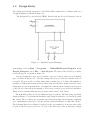
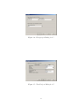
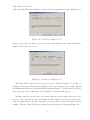
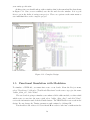
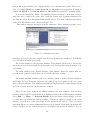
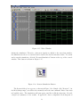
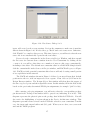
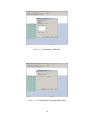
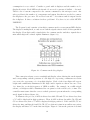
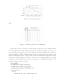
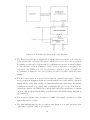
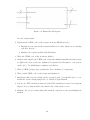
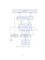
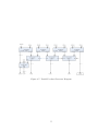
Digital Electronic Laboratory 2007: Digital Design
using FPGA Technology
by
Lucien Ngalamou
University of the West Indies, Copyright 2007
Abstract
This lab manual presents an introduction to the fundamental aspects of digital systems
design. The teaching approach undertaken aims at gradually exposing students to the
modern techniques of digital design through a series of labs and final project. The Project
is the mean by which students exercise the knowledge gained to design a decimal calculator
and its rapid prototyping on an FPGA board1 .
1
www.digilentinc.com
Contents
1 Introduction to VHDL Design using Xilinx ISE Tool
1.1 Objectives . . . . . . . . . . . . . . . . . . . . . . . . .
1.2 Bibliography . . . . . . . . . . . . . . . . . . . . . . . .
1.3 Project Navigator Overview . . . . . . . . . . . . . . .
1.4 Design Entry . . . . . . . . . . . . . . . . . . . . . . .
1.5 Functional Simulation with Modelsim . . . . . . . . . .
1.6 Design Synthesis . . . . . . . . . . . . . . . . . . . . .
1.7 Design Implementation . . . . . . . . . . . . . . . . . .
1.8 Timing Simulation . . . . . . . . . . . . . . . . . . . .
1.9 Programming the FPGA by Download Cable . . . . . .
1.10 Programming the PROM by Download Cable . . . . .
1.11 Extra question . . . . . . . . . . . . . . . . . . . . . .
1.12 References . . . . . . . . . . . . . . . . . . . . . . . . .
.
.
.
.
.
.
.
.
.
.
.
.
.
.
.
.
.
.
.
.
.
.
.
.
.
.
.
.
.
.
.
.
.
.
.
.
.
.
.
.
.
.
.
.
.
.
.
.
.
.
.
.
.
.
.
.
.
.
.
.
.
.
.
.
.
.
.
.
.
.
.
.
.
.
.
.
.
.
.
.
.
.
.
.
.
.
.
.
.
.
.
.
.
.
.
.
.
.
.
.
.
.
.
.
.
.
.
.
.
.
.
.
.
.
.
.
.
.
.
.
2 VHDL Design of a 2-bit Adder: Behavioral and Structural Methods
2.1 Objectives . . . . . . . . . . . . . . . . . . . . . . . . . . . . . . . . . . .
2.2 Sequential-Behavioral Architecture of a 2-bit Adder . . . . . . . . . . . .
2.3 Structural Architecture of a 2-bit Adder . . . . . . . . . . . . . . . . . .
2.4 Time Multiplexing of Displays . . . . . . . . . . . . . . . . . . . . . . . .
3 Keypad Encoder and Time-Multiplexing Display
3.1 Pre-lab . . . . . . . . . . . . . . . . . . . . . . . . .
3.1.1 Sequential-Behavioral Architecture of a 2-bit
3.1.2 Structural Architecture of a 2-bit Adder . .
3.2 Objectives . . . . . . . . . . . . . . . . . . . . . . .
3.3 Materials Needed . . . . . . . . . . . . . . . . . . .
3.4 Description . . . . . . . . . . . . . . . . . . . . . .
3.5 Time Multiplexing of Displays . . . . . . . . . . . .
3.6 Lab Exercises . . . . . . . . . . . . . . . . . . . . .
. . . .
Adder
. . . .
. . . .
. . . .
. . . .
. . . .
. . . .
.
.
.
.
.
.
.
.
.
.
.
.
.
.
.
.
.
.
.
.
.
.
.
.
.
.
.
.
.
.
.
.
.
.
.
.
.
.
.
.
.
.
.
.
.
.
.
.
.
.
.
.
.
.
.
.
.
.
.
.
.
.
.
.
.
.
.
.
.
.
.
.
.
.
.
.
1
1
2
2
5
10
14
15
19
20
26
30
31
.
.
.
.
32
32
32
32
33
.
.
.
.
.
.
.
.
38
38
38
38
39
39
39
41
45
4 Design Project: A Decimal Calculator
47
4.1 Introduction . . . . . . . . . . . . . . . . . . . . . . . . . . . . . . . . . . . 47
i
4.2
4.3
Design Approach . . . . . . . . . . . .
Project Description . . . . . . . . . . .
4.3.1 BCD Addition . . . . . . . . . .
4.3.2 BCD Subtraction . . . . . . . .
4.3.3 BCD Multiplication . . . . . . .
4.3.4 Project Integration and Testing
ii
.
.
.
.
.
.
.
.
.
.
.
.
.
.
.
.
.
.
.
.
.
.
.
.
.
.
.
.
.
.
.
.
.
.
.
.
.
.
.
.
.
.
.
.
.
.
.
.
.
.
.
.
.
.
.
.
.
.
.
.
.
.
.
.
.
.
.
.
.
.
.
.
.
.
.
.
.
.
.
.
.
.
.
.
.
.
.
.
.
.
.
.
.
.
.
.
.
.
.
.
.
.
.
.
.
.
.
.
.
.
.
.
.
.
.
.
.
.
.
.
47
47
49
50
50
51
List of Figures
1.1
1.2
1.3
1.4
1.5
1.6
1.7
1.8
1.9
1.10
1.11
1.12
1.13
1.14
1.15
1.16
1.17
1.18
1.19
1.20
1.21
1.22
1.23
1.24
1.25
1.26
1.27
1.28
1.29
1.30
1.31
1.32
Digilent Pegasus Kit . . . . . . . . . . . . . . . . . . .
Typical Project Navigator Windows . . . . . . . . . . .
Digilent Pegasus Kit Image . . . . . . . . . . . . . . .
New project Dialog 1 of 5 . . . . . . . . . . . . . . . .
New Project Dialog 2 of 5 . . . . . . . . . . . . . . . .
New Project Dialog 3 of 5 . . . . . . . . . . . . . . . .
New Project Dialog 4 of 5 . . . . . . . . . . . . . . . .
New Project Dialog 5 of 5 . . . . . . . . . . . . . . . .
New Project Dialog 1 of 2 . . . . . . . . . . . . . . . .
New Project Dialog 2 of 2 . . . . . . . . . . . . . . . .
Complete Design . . . . . . . . . . . . . . . . . . . . .
Test bench File Creation . . . . . . . . . . . . . . . . .
Testbench Timing Setting . . . . . . . . . . . . . . . .
Simulation Console . . . . . . . . . . . . . . . . . . . .
Wave Window . . . . . . . . . . . . . . . . . . . . . . .
Restart Simulation Button . . . . . . . . . . . . . . . .
Restart Dialog . . . . . . . . . . . . . . . . . . . . . . .
New Source Dialog 1 of 3 . . . . . . . . . . . . . . . . .
New Source Dialog 2 of 3 . . . . . . . . . . . . . . . . .
New Source Dialog 3 of 3 . . . . . . . . . . . . . . . . .
Entering Pin Location Constraints using PACE
Simulation Process Properties . . . . . . . . . . .
Generate Programming File Process Properties
Generate Programming File Process Properties
Download Cable Connection . . . . . . . . . . . . .
Configuration Mode Selection . . . . . . . . . . . .
Boundary-Scan Mode Selection . . . . . . . . . . .
Notification . . . . . . . . . . . . . . . . . . . . . . .
Selecting the FPGA Programming File . . . . . .
Placing the PROM in Bypass Mode . . . . . . . .
Select Program Device . . . . . . . . . . . . . . . .
Programming Options . . . . . . . . . . . . . . . .
iii
.
.
.
.
.
.
.
.
.
.
.
.
.
.
.
.
.
.
.
.
.
.
.
.
.
.
.
.
.
.
.
.
.
.
.
.
.
.
.
.
.
.
.
.
.
.
.
.
.
.
.
.
.
.
.
.
.
.
.
.
.
.
.
.
.
.
.
.
.
.
.
.
.
.
.
.
.
.
.
.
.
.
.
.
.
.
.
.
.
.
.
.
.
.
.
.
.
.
.
.
.
.
.
.
.
.
.
.
.
.
.
.
.
.
.
.
.
.
.
.
.
.
.
.
.
.
.
.
.
.
.
.
.
.
.
.
.
.
.
.
.
.
.
.
.
.
.
.
.
.
.
.
.
.
.
.
.
.
.
.
.
.
.
.
.
.
.
.
.
.
.
.
.
.
.
.
.
.
.
.
.
.
.
.
.
.
.
.
.
.
.
.
.
.
.
.
.
.
.
.
.
.
.
.
.
.
.
.
.
.
.
.
.
.
.
.
.
.
.
.
.
.
.
.
.
.
.
.
.
.
.
.
.
.
.
.
.
.
.
.
.
.
.
.
.
.
.
.
.
.
.
.
.
.
.
.
.
.
.
.
.
.
.
.
.
.
.
.
.
.
.
.
.
.
.
.
.
.
.
.
.
.
.
.
.
.
.
.
.
.
.
.
.
.
.
.
.
.
.
.
.
.
.
.
.
.
.
.
.
.
.
.
.
.
.
.
.
.
.
.
.
.
.
.
.
.
.
.
.
.
.
.
.
.
.
.
.
.
.
.
.
.
.
.
.
.
.
.
.
.
.
.
1
3
5
6
6
7
7
8
8
9
10
11
11
12
13
13
14
16
17
18
18
20
21
21
22
23
23
24
24
25
25
26
1.33
1.34
1.35
1.36
1.37
File Type Selection . . . . . . .
PROM Property Selection . . .
PROM Selection . . . . . . . . .
Summary Window . . . . . . . .
Add FPGA Programming Files
.
.
.
.
.
.
.
.
.
.
.
.
.
.
.
.
.
.
.
.
.
.
.
.
.
.
.
.
.
.
.
.
.
.
.
.
.
.
.
.
.
.
.
.
.
.
.
.
.
.
.
.
.
.
.
.
.
.
.
.
.
.
.
.
.
.
.
.
.
.
.
.
.
.
.
.
.
.
.
.
.
.
.
.
.
.
.
.
.
.
.
.
.
.
.
.
.
.
.
.
.
.
.
.
.
.
.
.
.
.
27
28
28
29
29
2.1
2.2
2.3
2.4
2.5
Enhanced 2-bit adder . . . . . . . .
Common anode detail . . . . . . .
Common anode Sseg display . . . .
Sseg signal timing . . . . . . . . . .
Cathode patterns for decimal digits
.
.
.
.
.
.
.
.
.
.
.
.
.
.
.
.
.
.
.
.
.
.
.
.
.
.
.
.
.
.
.
.
.
.
.
.
.
.
.
.
.
.
.
.
.
.
.
.
.
.
.
.
.
.
.
.
.
.
.
.
.
.
.
.
.
.
.
.
.
.
.
.
.
.
.
.
.
.
.
.
.
.
.
.
.
.
.
.
.
.
.
.
.
.
.
.
.
.
.
.
.
.
.
.
.
.
.
.
.
.
33
33
34
35
35
3.1
3.2
3.3
3.4
3.5
3.6
3.7
3.8
Enhanced 2-bit adder . . . . . . . . . . .
Debounce-free Keypad Decoder Diagram
Keypad decoder Module . . . . . . . . .
Common anode detail . . . . . . . . . .
Common anode Sseg display . . . . . . .
Sseg signal timing . . . . . . . . . . . . .
Cathode patterns for decimal digits . . .
Entity Block Diagram . . . . . . . . . .
.
.
.
.
.
.
.
.
.
.
.
.
.
.
.
.
.
.
.
.
.
.
.
.
.
.
.
.
.
.
.
.
.
.
.
.
.
.
.
.
.
.
.
.
.
.
.
.
.
.
.
.
.
.
.
.
.
.
.
.
.
.
.
.
.
.
.
.
.
.
.
.
.
.
.
.
.
.
.
.
.
.
.
.
.
.
.
.
.
.
.
.
.
.
.
.
.
.
.
.
.
.
.
.
.
.
.
.
.
.
.
.
.
.
.
.
.
.
.
.
.
.
.
.
.
.
.
.
.
.
.
.
.
.
.
.
.
.
.
.
.
.
.
.
.
.
.
.
.
.
.
.
39
40
41
42
43
43
44
46
4.1
4.2
4.3
4.4
4.5
4.6
4.7
Calculator Block Diagram . . . . . . . . . . .
BCD Arithmetic Module . . . . . . . . . . . .
BCD Addition Operations . . . . . . . . . . .
1-digit BCD Adder . . . . . . . . . . . . . . .
BCD Multiplication Operations . . . . . . . .
. Block diagram of a pipelined BCD Multiplier
Partial Product Generator Diagram . . . . . .
.
.
.
.
.
.
.
.
.
.
.
.
.
.
.
.
.
.
.
.
.
.
.
.
.
.
.
.
.
.
.
.
.
.
.
.
.
.
.
.
.
.
.
.
.
.
.
.
.
.
.
.
.
.
.
.
.
.
.
.
.
.
.
.
.
.
.
.
.
.
.
.
.
.
.
.
.
.
.
.
.
.
.
.
.
.
.
.
.
.
.
.
.
.
.
.
.
.
.
.
.
.
.
.
.
.
.
.
.
.
.
.
48
49
50
51
51
52
53
iv
Chapter 1
Introduction to VHDL Design using
Xilinx ISE Tool
1.1
Objectives
This lab is an introduction to logic design using VHDL with the Xilinx ISE Wepack tool.
No new logic design concepts are presented in this lab. The goals of this lab are for you
to become familiar with the tools you will be using for the rest of the semester:
- Xilinx’s ISE Project Navigator tool for VHDL.
- Diligent Pegasus Kit.
- Model Technology’s Modelsim simulator for VHDL.
Consider this lab as a "no-brainer" warm up for the next labs. Please read carefully, pay
attention, and take your time. This lab is not a race to see who gets done first. In order
to receive a bonus for this lab, you must demonstrate to the instructor that your final
design works correctly in hardware. The details of the required demonstration are at the
end of the lab handout. For this lab, no report is due. Section #8 can be omitted.
Figure 1.1: Digilent Pegasus Kit
1
1.2
Bibliography
This lab draws heavily from documents on the Xilinx website http://www.xilinx.com. The
lab leverages content from the ISE 6 In-Depth Tutorial, the ISE 6 Quick Start Tutorial,
and the Pegasus Kit Reference Manual. This lab is effectively a customized tutorial using
VHDL and the Pegasus Kit.
1.3
Project Navigator Overview
The Project Navigator is divided into four main sub-windows, as seen in figure 1.11. On
the top left is the Sources in Project window which hierarchically displays the elements
included in the project. Beneath the Sources in Project window is the Processes for Current Source window which displays available processes for the currently selected source.
The third window at the bottom of the Project Navigator is the Console window which
displays status messages, errors, and warnings, and which is updated during all project
actions. The fourth window to the right is for viewing and editing text files. Each window
may be resized, unlocked from Project Navigator or moved to a new location within the
main Project Navigator window. The default layout can always be restored by selecting
View —> Restore Default Layout.
The Sources in Project window consists of three tabs which provide information for
the user. Each tab is discussed in further detail below:
- The Module View tab displays the project name, any user documents, the specified
part type and design flow/synthesis tool, and design source files. Each file in the Module
View has an associated icon. The icon indicates the file type (VHDL file or text file, for
example). For a complete list of possible source types and their associated icons, see the
Project Navigator online help. Select Help ISE Help Contents, select the Index tab and
click Source / File types. If a file contains lower levels of hierarchy, the icon has a + to
the left of the name. VHDL files have this + to show the modules within the file. You can
expand the hierarchy by clicking the +. You can open a file for editing by double-clicking
on the filename.
- The Snapshot View tab displays all snapshots associated with the project currently
open in Project Navigator. A snapshot is a copy of the project including all files in the
working directory, and synthesis and simulation subdirectories. A snapshot is stored with
the project for which it was taken, and can be viewed in the Snapshot View. You can view
the reports, user documents, and source files for all snapshots. All information displayed
in the Snapshot View is read-only. Using snapshots provides an excellent version control
system.
- The Library View tab displays all libraries associated with the project open in Project
Navigator.
2
Figure 1.2: Typical Project Navigator Windows
3
The Processes for Current Source window contains the Process View tab. The Process
View tab is context sensitive and changes based upon the source type selected in the
Sources for Project window. From the Process View tab, you can run the functions necessary to define, run and view your design. The Process View tab provides access to the
following functions:
- Design Entry Utilities. Provides access to symbol generation, instantiation templates, HDL Converter, Command Line Log Files, Launch MTI, and simulation library
compilation.
- User Constraints. Provides access to editing location and timing constraints. indent - Synthesis. Provides access to Check Syntax, Synthesize, View RTL Schematic, and
synthesis reports. This varies depending on the synthesis tools you use.
- Implement Design. Provides access to implementation tools and design flow reports.
indent - Generate Programming File. Provides access to the configuration tools and bitstream generation.
The Processes for Current Source window incorporates automake technology. This
enables the user to select any process in the flow and the software automatically runs the
processes necessary to get to the desired step. For example, when you run the Implementation process, Project Navigator also runs the synthesis process, if necessary, because
implementation is dependent on up-to-date synthesis results.
The Console window displays errors, warnings, and informational messages. Errors
are signified by a red box next to the message, while warnings have a yellow box. Warning
and Error messages may also be viewed separately from other console text messages by
selecting either the Warnings or Errors tab at the bottom of the console window.
You can navigate from a synthesis error or warning message in the Console window
to the location of the error in a source VHDL file. To do so, select the error or warning
message, right-click the mouse, and from the menu select Goto Source. The VHDL source
file opens and the cursor moves to the line with the error.
You can also navigate from an error or warning message in the Console window to the
relevant solution records on the Xilinx support website. These types of errors or warnings
can be identified by the web icon to the left of the error. To navigate to the solution
record, select the error or warning message, right-click the mouse, and from the menu
select Goto Solution Record. The default web browser opens and displays all solution
records applicable to this message.
In the fourth window, you can access the ISE Text Editor, the ISE Language Templates, and HDL Bencher Text Editor. The ISE Text Editor enables you to edit source
files and to access the ISE Language Templates, which is a catalog of VHDL and User
Constraint File templates. You can use and modify these templates for your own design.
4
1.4
Design Entry
The design used in this tutorial is a 2-bit Full Adder enhanced by a disaply unit on a
7-segment display as shown in figure 2.2.
The design will be described in VHDL. Double-click the Project Navigator icon on
Figure 1.3: Digilent Pegasus Kit Image
your desktop or select Start –> Programs —> Xilinx ISE Project Navigator. From
Project Navigator, select File –> New Project. The first of the New Project dialog
boxes will appear, as shown in figure 1.4.
You are prompted to enter a project name, a project location, and a top level module
type, as shown in Figure 1.4. You may change the project location to another folder if
you wish. Do not use file or folder names that contain spaces. I advise all students to
purchase a USB memory stick and store their work on removable media. Even if you are
doing most of your work from home, you must have some means to transport your project
to the lab if you need help debugging it. Never store your projects on the lab machines.
When you are satisfied with the project name and location, click "Next".
The next dialog allows you to set additional project options. The first group of settings
shown in Figure 1.5 represents the hardware target that is available to you on the Pegasus
Kit board. The second group of settings represents the design entry language, synthesis
tool, and simulator preferences. Set the options as shown in Figure 1.5 and click "Next"’.
The following dialog box of Figure 1.6 gives you the opportunity to create new source files
as part of the new project process. Co not create new source files at this time, simply
5
Figure 1.4: New project Dialog 1 of 5
Figure 1.5: New Project Dialog 2 of 5
6
click "Next"’ to proceed.
The following dialog box of Figure 1.6 gives you the opportunity to add existing source
Figure 1.6: New Project Dialog 3 of 5
files as part of the new project process. Do not add existing source files at this time,
simply click "Next" to proceed.
Figure 1.7: New Project Dialog 4 of 5
The final dialog box in the new project process, shown in Figure 1.7, provides a
summary of the project that Project Navigator will create based on your settings. Review
the summary to make sure it matches what is shown in Figure 1.7. If it does not, go "Back"
and correct any errors. Otherwise, click "Finish"’ to complete this process.
At this point, the project has been created but it does not contain any source files.
Create a new source file for the 2-bit enhanced adder. Either select Project New Source
from the main menu or use the equivalent process in the Processes for Current Source
window. The first of the New Source dialog boxes will appear, as shown in Figure 1.8.
7
Figure 1.8: New Project Dialog 5 of 5
Figure 1.9: New Project Dialog 1 of 2
8
Select VHDL Module to indicate you are creating a Verilog-HDL design module. Then,
provide a file name as shown in Figure 1.9. You should not need to change the specified
location, which should be inside the project directory you created earlier. Click "Next"’.
The next dialog optionally allows you to specify the ports of the module. This may also
be done in the text editor, when creating the module, so skip it at this stage. Simply
confirm that the settings match those shown in Figure 1.10 and click "Next".
Figure 1.10: New Project Dialog 2 of 2
The final dialog box that will appear provides a summary of the source that Project
Navigator will create based on your settings. Click "Finish " to complete this process.
The new source file will be automatically opened in the text editor.
In the text editor, some of the basic file structure is already in place. Keywords
are displayed in blue, data types in red, comments in green, and values in black. This
color-coding enhances readability and recognition of typographical errors. Now, enter the
two-bit enhanced adder.
The code of the enhanced 2-bit adder is of the type "behavioral concurrent". Its code
was written three weeks ago during the studio presentation of VHL. For the Hex-to- 7
segment display; remember to use the Language templates from the Edit Menu: Edit –>
Language Templates –> VHDL –> Synthesis Templates —>HEX2LED Converter. Copy
and paste it into your VHDL code and change the name of its parameters according to
9
your entity specification.
At this point, you should end up with a window that looks somewhat like that shown
in Figure 1.11. Once you are satisfied, save the file and close the window. It is a good
idea to get in the habit of saving your project. There are options on the main menu to
save individual files or the complete project.
Figure 1.11: Complete Design
1.5
Functional Simulation with Modelsim
To simulate a VHDL file, you must first create a test bench. From the Project menu,
select "New Source", follow by "Test Bench Waveform" as the source type give the name
"adder_2bits_tb", click "Next".
The test bench is going to simulate your enhanced 2-bit adder module, so when asked
which source to associate the source with, select "adder_2bits_disp", and click "Next",
review the information and click the Finish button. The HDL Bencher now reads in the
design. Do not change the Timing parameters and continue by clicking OK.
You should set the values of vectors A and B in order to take into consideration the
10
Figure 1.12: Test bench File Creation
Figure 1.13: Testbench Timing Setting
11
sixteen different possibilities for 4 input variables of a combinational system. This can be
done by setting A[1:0] in a count up mode for 16 cycles incremented by 1 every 4
cycles and B[1:0] in a count up mode for 16 cycles incremented by 1 every cycle.
To start the simulation, double-click Simulate Behavioral Model. Modelsim creates a
work directory, compiles the source files, loads the design, and performs simulation for
the time specified. Four Modelsim windows will appear. The first, and most important,
is the main Modelsim console, shown in Figure 1.13.
This window displays messages from the simulator. These messages include notes,
Figure 1.14: Simulation Console
warnings, and errors, plus any output created by the design being simulated. You should
see text output from the test bench.
The second window is the structure window. This window allows you to browse the
hierarchy of the test bench and the design under test. In large hierarchical designs, it is
very handy.
The third window is the signals window. This window shows the signals that are
present in the portion of the design selected in the structure window.
The fourth and final window is the wave window, which is used to display simulated
waveforms. Project Navigator automatically adds all top-level signals to the wave window, as shown in Figure 1.14. Additional signals are displayed in the signal window based
upon the selected structure in the structure window.
There are two basic methods for adding signals to the wave window. You can drag
and drop them from the signals window, or highlight them in the signals window and then
select Add —> Wave —>Selected Signals. If you use this second technique, you will
see that there are additional options available. When you add new signals to the wave
window, you will notice that waveforms do not automatically appear. This is because
Modelsim did not record the simulation data for these signals. By default, Modelsim will
only record data for the signals that have been added to the waveform window before or
12
Figure 1.15: Wave Window
during the simulation. Therefore, when new signals are added to the waveform window,
the simulation needs to be restarted and re-run for the desired amount of time. To restart
and re-run the simulation, click the "Restart Simulation" button at the top of the console
window. This button is shown in Figure 1.15.
Figure 1.16: Restart Simulation Button
The Restart dialog box appears, as shown in Figure 1.16. Simply click "Restart"’. At
the Modelsim prompt, you will need to manually enter the run command. Enter "run 1000
ns"’and hit enter. The simulation will run again, just like it did the first time. Provide
a high level summary of the results. If applicable, show a simplified block diagram of
13
your design and highlight the critical path. If simulations were done, present the relevant
timing diagrams. Talk about the performance gained through your optimizations or
modifications.
Figure 1.17: Restart Dialog
1.6
Design Synthesis
With a functionally correct design description in VHDL, the next step is to use a synthesis tool to transform your description into a netlist. A netlist is a machine-readable
schematic. In this class, we will be using a tool called XST, which is integrated with
Project Navigator and can only target Xilinx devices. Select adder_2bits_disp in the
Sources in Project window. Then, double click on the Synthesize_XST process in the
Processes for Current Source window. Project Navigator will synthesize the design and
print information to the Console window in the process. As an informational note, it is
possible to change the synthesis options before you synthesize by right clicking on Synthesize_XST and then selecting Properties. For this tutorial, however, leave the options
at their default settings. You should not see any errors in the Console window. However,
you should always review the log file, which is available for viewing if you expand the
Synthesize_XST process item by clicking on the + next to it. Select View Synthesis
Report. If you donŠt understand a particular message, you should not simply ignore it.
Instead, search the Xilinx support web site or ask the instructor.
Reading the report is a good way to find out what types of (and how many) resources
the synthesis tool used. You can also catch other problems this way. For example, if you
14
found that this design description resulted in flip flops, in addition to a look-up table and
I/O buffers, you had better go back and figure out what went wrong. This is why you
must have an understanding of the hardware you are attempting to create when you write
your design description. At this point, you should have a green check mark next to the
Synthesize_XST process.
1.7
Design Implementation
Design implementation is the sequence of events that translates your synthesized design
netlist into a programming file for the FPGA device. Your design description, which you
have now synthesized, has a number of ports at the top level. The implementation tools
need to know how to assign the ports in your top level to physical pins on the FPGA,
which are connected to various resources on the Pegasus Kit board. If you do not make
explicit assignments, the tools will randomly assign pins for you. However, this is generally a bad idea because random assignments will be wrong.
The top-level design has 4 input ports (2-bit vectors A and B) and 12 output ports (
4-bit vector anode, 7-bit vector seg, and the carry out).
In order to get the ultimate performance from the device, you must tell the implementation tools what and where performance is required.
We will focus first on physical constraints or pin allocations. If you inspect the top
of the Pegasus Kit board, you will notice that almost every resource has been thoughtfully annotated with text indicating which FPGA pins are connected to it (in parentheses). This information is also available in the Pegasus Kit User’s Manual in tabular and
schematic form. Try to identify which FPGA pins are used for SW0, SW1, SW2, SW3,
AN3, AN2, AN1, AN0, seg(0), seg(1), seg(2), seg (3), seg(4), seg(5), seg(6), and LD0
(used for carry out), and then check your results with what is shown below. You will need
to be able to do this on your own in future lab assignments:
* SW0–> FPGA Pin 89: A(0)
* SW1–> FPGA Pin 88: A(1)
* SW2–> FPGA Pin 87: B(0)
* SW3–> FPGA Pin 86: B(1)
* AN0–> FPGA Pin 60: anode(0)
* AN1–> FPGA Pin 69: anode(1)
* AN2–> FPGA Pin 71: anode(2)
* AN3–> FPGA Pin 75: anode(3)
* seg(0)–> FPGA Pin 74
* seg(1)–> FPGA Pin 70
* seg(2)–> FPGA Pin 67
15
* seg(3)–> FPGA Pin 62
* seg(4)–> FPGA Pin 61
* seg(5)–> FPGA Pin 73
* seg(6)–> FPGA Pin 68
LD0–> FPGA Pin 46: Cout
You now have enough information to create what is called a user constraint file, or
UCF. This file contains design constraints that you did not specify in the VHDL description, such as pin location and design performance constraints. It is convenient to provide
them in a UCF rather than in the Verilog-HDL description. For instance, if you make a
mistake in the pin assignments, you do not need to go back and resynthesize your design.
You can add a UCF to the project using the same process you used for adding the design
and its test bench. Create a new source file; select Project –> New Source from the main
menu or use the equivalent process in the Processes for Current Source window. The first
of the New Source dialog boxes will appear, as shown in Figure 1.17.
Figure 1.18: New Source Dialog 1 of 3
Select Implementation Constraints File to indicate you are creating a constraints file.
Then, provide a file name as shown in Figure 1.18. You should not need to change the
specified location, which should be inside the project directory you created earlier. Click
"Next".
The second dialog, shown in Figure 1.19, asks you to identify a design module with
which the constraints file should be associated. Select the adder_2bits_disp design as
shown and click "Next".
The final dialog box of Figure 1.20 provides a summary of the source that Project Nav16
Figure 1.19: New Source Dialog 2 of 3
igator will create based on your settings. Review the summary to make sure it matches
what is shown in Figure 1.20. If it does not, go "Back" and correct any errors. Otherwise,
click "Finish"’ to complete this process. This time, however, you will notice that the new
source file is not automatically opened in the text editor.
If you select the constraint file in the Sources in Project Window, and then expand
the Processes for Current Source window item for User Constraints by clicking on the
+ next to it, you will see that there are a number of ways to edit a user constraint file,
including a text editor. The default user constraint editor is called PACE. Simply double
click the constraint file in the Sources in Project window, and PACE will open, see Figure
1.21. PACE is a fairly powerful constraint editor but we will only be using a small portion
of its capabilities in this tutorial.
The PACE sub-windows shown in Figure 1.21 have been moved from their default
positions in order to yield an improved screen capture. First click on I/O Pins in the
Design Browser window. The Design Object List window will then show the names of
the three top level ports and their signal directions. In this window, fill in the LOC fields
based on the previously determined FPGA pin assignments, for example "p89" for A(0).
After entering each pin assignment, you will notice that the corresponding package
pin shown in the Package Pins window will be grayed out, indicating it is in use. This
diagram represents the physical pins on the package that holds the FPGA die. You will
also notice the highlighting of regions shown in the Device Architecture window. This
diagram represents resources in use on the FPGA die related to your constraints Ű in this
case, the input and output buffers and I/O pads. When you are done, save your work
and exit the PACE program.
17
Figure 1.20: New Source Dialog 3 of 3
Figure 1.21: Entering Pin Location Constraints using PACE
18
Now that you have a constraint file in your project, you can implement the design.
Select adder_2bits_disp in the Sources in Project window. Then, double click on the Implement Design process in the Processes for Current Source window. Project Navigator
will implement the design and print information to the Console window in the process.
As an informational note, it is possible to change the implementation options before you
implement by right clicking on Implement Design and then selecting Properties. For this
tutorial, however, leave the options at their default settings.
You should not see any errors in the Console window. However, you should always
review the three log files, which are available for viewing if you expand the Implement
Design process item by clicking on the + next to it. There are log files located under
Translate, Map, and Place and Route. If you donŠt understand a particular message,
you should not simply ignore it. Instead, search the Xilinx support web site or ask the
instructor. At this point, you should have a green checkmark next to the Implement
Design process.
1.8
Timing Simulation
After completing the implementation steps, you can simulate your design again this time,
using a structural representation of your synthesized, placed, and routed design with
worstcase delay information. The idea is to simulate your design, as physically implemented in the FPGA device.
The simulation processes enable you to run simulation on the design using Modelsim.
To locate the Modelsim simulator processes, select the test bench in the Sources in Project
window. Then, click the + next to the Modelsim Simulator entry in the Processes for
Source window to expand the item. You will perform a timing simulation using Simulate
Post-Place & Route Verilog Model but you must specify the simulation process properties
first, just like you did for functional simulation. Right click on Simulate Post-Place &
Route VHDL Model, and select Simulation Properties. The Process Properties dialog
box appears, as shown in Figure 1.22.
Make sure the properties are set as shown in Figure 1.22. The most interesting of
these parameters is probably the simulation run time_again, 1000 ns is more than sufficient for the test bench in the project. For test benches that require more simulation
time, this property should be adjusted as needed. Click "Ok".
To start the simulation, double-click Simulate Post-Place & Route Verilog Model. Modelsim creates a work
directory, compiles the source files, loads the design, and performs simulation for the time
specified. The simulator will run, and you’ll see results as before. Are the simulation
results different from the previous ones? Explain. What are the type of hazards present
19
Figure 1.22: Simulation Process Properties
at carry out? Do they influence what is seen at LD0?
At this point, you are ready to program the FPGA with your design. The Pegasus Kit
board may be programmed by two different methods. One is to program the FPGA by
download cable. The other is to program the PROM by download cable, and then have
the PROM program the FPGA. Both are covered in the following sections.
1.9
Programming the FPGA by Download Cable
Programming the FPGA directly by the download cable is a convenient way to try out a
design. This method is useful when you want to quickly test something, or are not certain
your design is final. For example, at this point you are fairly confident your design is
correct. However, you should realize by this point in your education that complex designs
rarely ever work "on the first try". One of the great advantages FPGAs have over ASICs
is that the penalty for being wrong on the first try is minimal.
The first order of business is to create a programming file for the FPGA. Select
adder_2bits_disp in the Sources in Project window. In the Processes for Current Source
window, right click on Generate Programming File and then select Properties. The Process Properties dialog box appears. Select the Configuration Options tab, as shown in
Figure 1.23.
Change the Unused IOB Pins option to Float. The other settings should already be
correct, but make sure they match what is shown in Figure 1.23 Next, select the Startup
Options tab, as shown in Figure 24.
Change the FPGA Start-Up Clock option to JTAG Clock. The other settings should
already be correct, but make sure they match what is shown in Figure 1.24. Click "Ok"’
to save the settings. Confirm that adder_2bits_disp is selected in the Sources in Project
20
Figure 1.23: Generate Programming File Process Properties
Figure 1.24: Generate Programming File Process Properties
21
window. Then, double click on the Generate Programming File process in the Processes
for Current Source window. Project Navigator will generate a programming file and print
information to the Console window in the process.
Before you continue, you must have the Pegasus Kit board, power supply, and download cable available. Connect the download cable to the parallel port of the machine
you are using. Plug the power supply into the wall.connect the download cable to its
connector, as shown in Figure 1.25.
To download your bitstream to the FPGA device, expand the Generate Programming
Figure 1.25: Download Cable Connection
File process by clicking on the + next to it, and then double click on the Configure Device
(iMPACT) process. This will launch the iMPACT program in another window. You will
be immediately presented with several dialog boxes, the first of which is shown in Figure
1.26.
There are actually a bewildering number of ways to configure an FPGA device. The
board has an integrated JTAG programming function, which is also called Boundary-Scan
mode. Select this option and proceed to the next dialog box, shown in Figure 1.27.
Allow the program to automatically connect to the cable and identify the devices
on the board. After you finish this sequence, the program will automatically detect the
FPGA and PROM devices and prompt you to specify a programming file for each device.
You should see a message like that shown in Figure 1.28. Click "OK".
In the first file requester, shown in Figure 1.29, right click on "xc250...File..?", select
the adder_2bits_disp.bit file you created with the implementation process. This is the
FPGA programming file. Click "OPEN".
If you right click on "xcf01s...File..?", you will obtain the next file requester, shown in
22
Figure 1.26: Configuration Mode Selection
Figure 1.27: Boundary-Scan Mode Selection
23
Figure 1.28: Notification
Figure 1.29: Selecting the FPGA Programming File
24
Figure 1.30, asks for a PROM programming file. We are not programming the PROM at
this time, therefore select Bypass.
Finally, you will reach the point shown in Figure 1.31. iMPACT is ready to program
Figure 1.30: Placing the PROM in Bypass Mode
the FPGA. Select the FPGA icon in the window and then use the right mouse button to
activate the menu as shown and select the Program option.
Figure 1.31: Select Program Device
You will be presented with a dialog box listing programming options. Most of these
options are ghosted out for FPGA programming and are of no concern, see Figure 1.32.
25
Disable the Verify option, if selected, and then click "Ok" to start the programming
sequence.
A progress indicator will appear. Once the programming is complete, the program
Figure 1.32: Programming Options
will be sure to let you know if it was successful or if it failed. If the programming has
failed, re-check your cable connections, the power connections, and the jumpers, and then
try again. If it still fails, ask the instructor for assistance.
Now, you can test your design in hardware. Locate SW0, SW1, SW2, and SW3 on the
board, and exercise your design by trying the four possible combinations of switch settings
while observing LD0 and the rightmost 7-segment display. Does the circuit behave as you
expect? If it does not, seek assistance. If it does work properly, you are ready to try the
other programming method. Exit iMPACT (you do not need to save). Keep the board
connected to power and the download cable.
1.10
Programming the PROM by Download Cable
The other method is to program the PROM by download cable, and then have the PROM
program the FPGA. Typically you would program the PROM when you believe your
26
design is completely done. After the PROM is programmed, each time the power is
cycled, the FPGA will automatically load the programming file from the PROM. After
the PROM is programmed, the need for the download cable is eliminated.
Expand the Generate Programming File process by clicking on the + next to it, and
then double click on the Generate PROM, ACE, or JTAG File process. This will launch
the iMPACT program again.
Figure 1.33: File Type Selection
You will be immediately presented with several dialog boxes, the first of which is
shown in Figure 1.33. Select the PROM File option and proceed to the next dialog box,
shown in Figure 34.
In the dialog box of Figure 1.34, change the settings to match those shown. Do not
forget to change the PROM File Name. Then proceed to the next dialog box.
In the dialog box of Figure 1.35, select the XCF02S PROM type, and then click "Add".
You should see the PROM listed in the sub-window, at position zero. Then click "Next".
Figure 1.36 shows a summary of what you have selected. If your results do not match
that shown in Figure 36, go "Back" and correct your error. Otherwise, click "Next" to
proceed.
In the dialog box of Figure 1.37, click "Add File" When the file requester dialog
box appears, select the adder_2bits_disp.bit file, which is the same one you used before.
You will receive a warning that iMPACT needed to change the startup clock; dismiss the
warning. You may recall, from a previous step, that we set the Startup Clock option to
JTAG Clock when creating the programming file. This setting is required when programming the FPGA directly by the cable, but for programming the PROM the CCLK setting
27
Figure 1.34: PROM Property Selection
Figure 1.35: PROM Selection
28
Figure 1.36: Summary Window
Figure 1.37: Add FPGA Programming Files
29
should be used. iMPACT makes this change for you without requiring that you revisit
the Generate Programming File process.
After you add the adder_2bits_disp.bit file, iMPACT will ask you if you want to add
another design file to the PROM data stream. Click "No". You will see another dialog
box, which instructs you to click "Finish" to start generating the PROM file. Click "Finish". iMPACT will ask you if you want to create the file now. Click "Yes".
You have now created the PROM programming file. You need to program the PROM.
From the iMPACT main menu, select Mode –> Configuration Mode. Then, select File
–> Initialize Chain. At this point, you will be prompted for programming files for the
two devices in the chain, just like you were in the previous section. However, this time
around, put the FPGA in Bypass mode and assign the adder_2bits_disp.mcs file to the
PROM. Then, select the PROM icon, right click, and select Program and "OK"’ to start
the programming sequence.
A progress indicator will appear. Once the programming is complete, the program
will be sure to let you know if it was successful or if it failed. If the programming has
failed, re-check your cable connections, the power connections, and the jumpers; and then
try again. If it still fails, ask the instructor for assistance.
Now, you can test your design again. Exit iMPACT (you do not need to save). Unplug
the download cable from the board. Unplug the power supply, wait three seconds, and
then reapply power. The FPGA should load your design automatically from the PROM.
To verify it worked properly, locate SW0 , SW1, Sw2, and SW3 on the board, and exercise
your design by trying the four possible combinations of switch settings while observing
LD0. Does the circuit behave as you expect? If it does not, seek assistance. If it does
work properly, you are done with the lab. In order to receive credit, demonstrate your
final result to the instructor.
Other aspects such as the state machine and schematic editors will be covered later in
this class.
1.11
Extra question
While testing your design you have realized that the maximum value being displayed on
the rightmost 7-segment Led is 3, modify your code so that the display result contains
the 2-bit sum and carry out. You will then have on the display values that range from 0
to 6.
30
1.12
References
- Xilinx 6 In-Depth Tutorial
- Pegasus User’s Manual
- San Jose State University, Dept. of Electrical Engineering, EE178 Laboratory 1
31
Chapter 2
VHDL Design of a 2-bit Adder:
Behavioral and Structural Methods
2.1
Objectives
In the previous lab, we learned how to use Xilinx ISE in order to create, simulate,
and synthesize VHDL models of digital circuits. We used in our example the design of a
2-bits adder, whose architecture was of the type concurrent behavioral.
We will use the same example and write its architecture in two forms, that are the
behavioral sequential architecture and the structural architecture. For the structural
approach you will have to use the concept of package. The second part of the lab is
related to time multiplexing of data for 7-segment displays. A set of template codes for
this lab are provided on the course web site. Download and unzip them in your working
directory.
2.2
Sequential-Behavioral Architecture of a 2-bit Adder
The design being used in this part of the lab is a 2-bit Full Adder enhanced by a
7-segment display unit as shown in figure 2.1.
Start Xilinx ISE and open the project file adder_2bitsseq.npl, complete its vhdl
code, run a simulation, and use the constraint file of the previous lab for synthesis/implementation
. Program the FPGA board and test that your design is working. Before moving to the
next part of the lab exercise your TA must signed the check off sheet.
2.3
Structural Architecture of a 2-bit Adder
Open the project adder_2bitsstruct.npl. Following the same procedure of the
previous section. The difference here is that you have to complete your code using the
concept of component instantiation.
32
Figure 2.1: Enhanced 2-bit adder
You are advised to edit the file pckg_adder.vhd and see how it’s constructed. This
concept will be useful to you later in this class.
2.4
Time Multiplexing of Displays
Seven-segment displays are now widely used in almost all microprocessor-based instruments. A single seven-segment display can display the digits from 0 to 9 and the hex
digits A to F. Each display is composed of seven LEDs that are arranged in a way to
allow the display of different digits using different combinations of LEDs (figure 2.2).
Figure 2.2: Common anode detail
Since the display is composed of LEDs, which need high current to drive them, power
33
consumption is very critical. Consider a panel with 4 displays and the number to be
displayed is 8888. Each LED needs 20 mA. So we need a current of 20x7x4 = 560 mA.
That’s a lot of current compared to the current consumed by the microprocessor. Another problem is the number of components and output bits that are needed to connect
the displays to the processor. We need at least 4x7 = 28 resistors and 28 output bits for
the 4 displays. Is there a solution for these problems? Yes, there is, it’s called MULTIPLEXING!
The Pegasus board contains a four-digit common anode seven-segment LED display.
The display is multiplexed, so only seven cathode signals exist to drive all 28 segments in
the display. Four digit-enable signals drive the common anodes and these signals determine which digit the cathode signals illuminate (figure 2.3).
Figure 2.3: Common anode Sseg display
This connection scheme creates a multiplexed display, where driving the anode signals
and corresponding cathode patterns of each digit in a repeating, continuous succession
can create the appearance of a four-digit display. Each of the four digits will appear
bright and continuously illuminated if the digit enable signals are driven low once every
1 to 16ms (for a refresh frequency of 1KHz to 60Hz). For example, in a 60Hz refresh
scheme, each digit would be illuminated for one quarter of the refresh cycle, or 4ms. The
controller must assure that the correct cathode pattern is present when the corresponding
anode signal is driven (figure 2.4).
To illustrate the process, if AN0 is driven low while CB and CC are driven low, then
a "1" will be displayed in digit position 0. Then, if AN1 is driven low while CA, CB and
CC are driven low, then a "7"will be displayed in digit position 1. If A1 and CB, CC are
driven for 4ms, and then A2 and CA, CB, CC are driven for 4ms in an endless succession,
the display will show "17" in the first two digits. Figure 2.5 shows the pattern of decimal
34
Figure 2.4: Sseg signal timing
digit.
Figure 2.5: Cathode patterns for decimal digits
In this lab exercise we will all the 8 slide switches as inputs in order to displays simultaneously numbers 00 to FF in hexadecimal on two 7-segment displays (#2 and #1) or
two among the four available. We need for this purpose an input signals whose frequency
varies from 60Hz to 1KHz. The first thing one has to consider when approaching a new
design are the inputs and the outputs of the circuit. The assignment requires the control
of the seven segment displays. In order to control the seven segment displays, one needs
4 signals for activating the anodes and seven signals for controlling the cathodes. The
entity declaration is given as follows:
library IEEE;
use IEEE.STD_LOGIC_1164.ALL;
use IEEE.STD_LOGIC_ARITH.ALL;
use IEEE.STD_LOGIC_UNSIGNED.ALL;
entity mux7seg is
Port (
muxclk: in std_logic; – multiplexing clock
35
areset: in std_logic; – asynchronous reset
switchs : in std_logic_vector(7 downto 0); – slide switches inputs
sseg : out std_logic_vector(6 downto 0); – 7-segement leds
a : buffer std_logic_vector(3 downto 0)); – selection of the 7-segment
end mux7seg;
The function of the circuit is described in the architecture. There are certain considerations that have to be taken into account.
- Only one of the seven segment displays can be active at a time (see Fig. 8). It is
selected by the output signal a. The signal a can have at a single given moment only one
value like 1110, 1101, 1011, or 0111. This function can be implemented by a shift register
with a parallel load. The shifting operation of this shift register must be clocked by an
internal clock signal with a period between 0.25 ms and 4 ms. Let it be 1 ms. The input
clock is at 50 MHz, so it must be divided by 50000 in order to get an internal clock of
1000 Hz (1 ms period).
- If the signal a is 1110 (selecting display #1), then only bits 3 downto 0 are displayed. If a=1101, then bits 7 downto 4 are displayed (display#2). This means that the
upper and lower 4 bits coming from the 8 switches SW7 to SW0 must be multiplexed to
the decoder for the seven segment display. In all other cases the control signals sseg must
be set to ’1’ in order to turn off the diodes. There are three processes associated with
displaying the result from input data (8 switches): (1) select the seven segment display;
(2) select the four bits to decode; (3) decode the bits.
- The shifting process is synchronized with the muxclk signal, and is reset by the
asynchronous signal areset. You can think of it as a shift register. The shifting can be
expressed with a construct like this:
a <= (a(0) & a(3 downto 1)); Remember to load a with an initial value of say
1110, when areset is high.
- The multiplexing process is sensitive to the changes both in the displayed signal(data from the input switches) and in the selection signal a. The multiplexing can be
done with a case construct:
case a is
when "1110" => disp_led <= ...
...
end case;
Notice that bits to decode must be an internal signal with which the multiplexing and
the decoding processes will communicate with each other.
- The decoding process is sensitive to changes in the selected display (changes in
a) and to changes in the displayed value (bits to decode). The project file to be used here
is mux7seg_lab3.npl.
For implementation purposes use the pin configuration that was given in lab #2.
Muxclk is allocated to pin #77 and areset to pin #59.
36
Write the VHDL code of the multiplexing display, simulate it, synthesize and test it
on the FPGA board. In your report, you will have to add the complete code and the
simulation result.
Can we use NPN transistors instead of the PNP transistors for the seven-segment
display? If yes, what would be the initial value of the anode vector?
Estimate the power saving using this method compared to the non-multiplexed method.
37
Chapter 3
Keypad Encoder and
Time-Multiplexing Display
3.1
Pre-lab
In the previous lab, we learned how to use Xilinx ISE in order to create, simulate, and
synthesize VHDL models of digital circuits. We used in our example the design of a 2-bit
adder that has a concurrent behavioral architecture.
We will use the same example and write its architecture in two forms, which are
the behavioral sequential architecture and the structural architecture. For the structural
approach you will have to use the concept of package.
3.1.1
Sequential-Behavioral Architecture of a 2-bit Adder
The design being used in this part of the lab is a 2-bit Full Adder enhanced by a
7-segment display unit as shown in figure 3.1.1.
Start Xilinx ISE and open the project file adder_2bitsseq.npl, complete its vhdl
code, run a simulation, and use the constraint file of the previous lab for synthesis/implementation
. Program the FPGA board and test that your design is working. Before moving to the
next part of the lab exercise your TA must signed the check off sheet.
3.1.2
Structural Architecture of a 2-bit Adder
Open the project adder_2bitsstruct.npl. Following the same procedure of the
previous section. The difference here is that you have to complete your code using the
concept of component instantiation.
You are advised to edit the file pckg_adder.vhd and see how it’s constructed. This
concept will be useful to you later in your subsequent Labs and EE17D Project.
38
Figure 3.1: Enhanced 2-bit adder
3.2
Objectives
This lab exercise deals with the design of a keypad encoder and a time-multiplexing
display. This is a good "jumpstart" for your EE17D Project. You are advised to use the
structural approach in your design. Each submodule must be coded/simulated. Next,
you have to organize your simulated submodules as a package of components. Finally use
the concept of component instantiation to complete your final design.
3.3
Materials Needed
1. The Pegasus Board
2. A 3 x 4 Keypad and an array of 10 resistors with a common pin (2). These two
modules are integrated in a proto board.
3.4
Description
Consider figure 3.2 which consists of a keypad encoder, a key-code register, and a timemultiplexing display decoder. The functionalities of the different elements are given as
follows:
39
Figure 3.2: Debounce-free Keypad Decoder Diagram
• The Keypad encoder has 13 inputs and 4 outputs that represent the code of the key
being pressed and a detector "Keypress" which is set to one once a key is pressed.
It consists of a debounce element and of a combinational encoder as shown in figure
3. The debounce element eliminates contact bounces that may occur when a key
is pressed. The VHDL code of a 1-bit debounce element is given , you will have
to customize it using the concept of package in order to build a 12-bit debounce
module.
• The key-code register is a special 16-bit shift-left parallel load register. When a
key is pressed its rightmost 4 bits are loaded with the new value and its content is
shifted left by 4 bits. This register accommodates four successive keys. Its internal
organization is made of a counter that re-initializes the process once four keys are
pressed successively. Its VHDL code is given. In Your lab report will have to explain
on your own words its functionality, together with a Modelsim timing diagram of
its simulation.
• The frequency divider takes as input a 50 MHz clock signal a produces a 1 kHz
signal (division by 50,000).
• The time-multiplexing decoder recognizes only digits 0 to 9 and generates their
equivalent 7-segment codes at its outputs.
40
• The reset signal must be buffered using the IBUF component, the output of IBUF
is then used as the real reset signal.
The internal structure of the keypad encoder is given in figure 3.3
Figure 3.3: Keypad decoder Module
Table 3.1 shows the data format that is recognized by the keypad encoder:
3.5
Time Multiplexing of Displays
Seven-segment displays are now widely used in almost all microprocessor-based instruments. A single seven-segment display can display the digits from 0 to 9 and the hex
digits A to F. Each display is composed of seven LEDs that are arranged in a way to
allow the display of different digits using different combinations of LEDs (figure 3.5).
Since the display is composed of LEDs, which need high current to drive them, power
consumption is very critical. Consider a panel with 4 displays and the number to be
displayed is 8888. Each LED needs 20 mA. So we need a current of 20x7x4 = 560 mA.
That’s a lot of current compared to the current consumed by the microprocessor. Another problem is the number of components and output bits that are needed to connect
the displays to the processor. We need at least 4x7 = 28 resistors and 28 output bits for
the 4 displays. Is there a solution for these problems? Yes, there is, it’s called MULTIPLEXING!
41
Key
Character
*
7
4
1
0
8
5
2
#
9
6
3
Equivalent 12-Bit
Code Output
Key
Pin#
Connector FPGA
A2 Pin#
Pin#
1000
0100
0010
0001
0000
0000
0000
0000
0000
0000
0000
0000
2
3
4
5
6
7
8
9
10
11
12
13
1(+3.3 V)
21
20
19
18
17
16
15
14
13
12
11
10
0000
0000
0000
0000
1000
0100
0010
0001
0000
0000
0000
0000
0000
0000
0000
0000
0000
0000
0000
0000
1000
0100
0010
0001
162
163
164
165
166
167
168
172
173
174
175
176
Table 3.1: Keypad Character Code
Figure 3.4: Common anode detail
The Pegasus board contains a four-digit common anode seven-segment LED display.
The display is multiplexed, so only seven cathode signals exist to drive all 28 segments
in the display. Four digit-enable signals drive the common anodes and these signals
determine which digit the cathode signals illuminate (figure 3.5).
This connection scheme creates a multiplexed display, where driving the anode signals
and corresponding cathode patterns of each digit in a repeating, continuous succession
can create the appearance of a four-digit display. Each of the four digits will appear
bright and continuously illuminated if the digit enable signals are driven low once every
1 to 16ms (for a refresh frequency of 1KHz to 60Hz). For example, in a 60Hz refresh
scheme, each digit would be illuminated for one quarter of the refresh cycle, or 4ms. The
controller must assure that the correct cathode pattern is present when the corresponding
anode signal is driven (figure 3.5).
To illustrate the process, if AN0 is driven low while CB and CC are driven low, then
a "1" will be displayed in digit position 0. Then, if AN1 is driven low while CA, CB and
42
Figure 3.5: Common anode Sseg display
Figure 3.6: Sseg signal timing
CC are driven low, then a "‘7"will be displayed in digit position 1. If A1 and CB, CC are
driven for 4ms, and then A2 and CA, CB, CC are driven for 4ms in an endless succession,
the display will show "‘17" in the first two digits. Figure 3.5 shows the pattern of decimal
digit.
43
Figure 3.7: Cathode patterns for decimal digits
The output of the key-code register (0000 to 9999) should be displayed simultaneously on the four 7-segment displays available. We need for this purpose an input signals
whose frequency varies from 60Hz to 1KHz. The first thing one has to consider when
approaching a new design are the inputs and the outputs of the circuit. The assignment
requires the control of the seven segment displays. In order to control the seven segment
displays, one needs 4 signals for activating the anodes and seven signals for controlling
the cathodes.
The entity declaration is given as follows:
library IEEE;
use IEEE.STD_LOGIC_1164.ALL;
use IEEE.STD_LOGIC_ARITH.ALL;
use IEEE.STD_LOGIC_UNSIGNED.ALL;
entity mux7seg is
Port (
muxclk: in std_logic; – multiplexing clock
areset: in std_logic; – asynchronous reset
switchs : in std_logic_vector(15 downto 0); – data inputs
sseg : out std_logic_vector(6 downto 0); – 7-segement leds
a : buffer std_logic_vector(3 downto 0)); – selection of the 7-segment
end mux7seg;
The function of the circuit is described in the architecture. There are certain considerations that have to be taken into account.
- Only one of the seven segment displays can be active at a time (see Fig. 6). It is
selected by the output signal a. The signal a can have at a single given moment only one
value like 1110, 1101, 1011, or 0111. This function can be implemented by a shift register
with a parallel load. The shifting operation of this shift register must be clocked by an
internal clock signal with a period between 0.25 ms and 4 ms. Let it be 1 ms. The input
44
clock is at 50 MHz, so it must be divided by 50000 in order to get an internal clock of
1000 Hz (1 ms period).
- If the signal a is 1110 (selecting display #1), then only bits 3 downto 0 are displayed. If a=1101, then bits 7 downto 4 are displayed (display#2), up to 0111 for the
display of bits 15 downto 0. This means that the key-code register outputs must be multiplexed to the decoder for the seven segment display. In all other cases the control signals
sseg must be set to ’1’ in order to turn off the diodes. There are three processes associated
with displaying the key-code register data : (1) select the seven segment display; (2) select
the four bits to decode; (3) decode the bits.
- The shifting process is synchronized with the muxclk signal, and is reset by the
asynchronous signal areset. You can think of it as a shift register. The shifting can be
expressed with a construct like this:
a <= (a(0) & a(3 downto 1)); Remember to load a with an initial value of say
1110, when areset is high.
- The multiplexing process is sensitive to the changes
both in the displayed signal(data from the input switches) and in the selection signal a.
The multiplexing can be done with a case construct:
case a is
when "1110" => disp_led <= ...
...
end case;
Notice that bits to decode must be an internal signal with which the multiplexing and
the decoding processes will communicate with each other.
The decoding process is sensitive to changes in the selected display (changes in a) and to
changes in the displayed value (bits to decode). Use the project file mux7seg_lab3.npl
to test this module.
For implementation purposes use the pin configuration that was given in lab #3.
3.6
Lab Exercises
At the beginning of your coding process, you must have a good understanding of the
design in terms of its interface (entity) and architecture. Figure 3.6 gives you a block diagram of the system. Your report contain have the complete VHDL code of all the modules
you have implemented and their relevant simulation results. The pre-lab is compulsory
and must be added to your report.
1. Analyze and write a VHDL model of the KeyPad Encoder, use for this purpose
the basic debounce code that is posted on the course web site. Use Moldelsim to
simulate its behavior. Keys * and # are not considered to be valid codes (the
45
Figure 3.8: Entity Block Diagram
decoder outputs 0000).
2. Download the VHDL code of the register from the EE19D web site:
• Explain on your own words its functionality (to be done when you are writing
your Lab Report).
• Simulate the register module with Modelsim.
3. Write the VHDL code of the frequency divider.
4. Analyze and complete the VHDL code of the time-multiplexing Encoder that is used
to display the keys on the two rightmost 7-segment leds (Incomplete code posted
on the web). Use Moldelsim to simulate its behavior.
5. Write a VHDL package that contains the above modules as components.
6. Write a final VHDL code of the design and simulate it.
7. Implement and test your design on the pegasus board. You should create a constraint file for the design using table #1 and the Pegaus Manual.
8. Can we use NPN transistors instead of the PNP transistors for the seven-segment
display? If yes, what would be the initial value of the anode vector?
9. Estimate the power saving using this method compared to the non-multiplexed
method.
46
Chapter 4
Design Project: A Decimal Calculator
4.1
Introduction
One important electronic device commonly used by high-school students is a scientific
calculator. This project investigates the digital design of a pocket calculator that allows
three basic arithmetic operations (+, -, *) on integers. In order to reduce the complexity
of your design the range of numbers to be used by your calculator is 0 to 9999.
4.2
Design Approach
For this design we will use a FPGA board as the target architecture and Xiinx ISE/Modelsim
as the software development platform. We consider the following steps that are crucial
for the project completion:
1. Modular analysis and implementation of the system.
2. Analysis of electrical properties (power consumption, operating frequency, size on
chip).
3. Implementation and testing of the final design.
4. Writing of a small user manual to be included in your project report.
4.3
Project Description
The block diagram of figure 4.1 gives a general overview of the design to be implemented.
The system is made of combinational modules (adder, subtractor, encoders, ..) and
sequential modules (arithmetic controller, frequency divider, control processes for the
time-multiplexing display and keypad encoder). We can identify the following operative
steps for the calculator:
• entering operands and operators via a 4 x 3 key pad,
47
• decoding of the data entered trough the key pad,
• realization of the selected arithmetic operation,
• display of the results.
The system is made of the following elements as shown in figure 4.2:
• A debounce-free keypad encoder, which an improvement version of the one you
designed in Lab 4.
• A time-multiplexing display.
• An Arithmetic unit that performs addition, subtraction, and multiplication on BCD
numbers.
• A frequency divider for the generation of the appropriate clock signals.
• The operation code is entered via the slide switches SW0 and SW1 on the FPGA
board (00: no operation, 01: +, 10: -, 11: *).
4.3.1
BCD Addition
The BCD adder is a 4-digit BCD adder that receives four BCD digits, performs addition on
them, and returns the result in a BCD format. Either packed or unpacked BCD numbers
can be summed. BCD addition follows the same rules as binary addition (textbook).
However, if the addition produces a carry and/or creates an invalid BCD number, an
adjustment is required to correct the sum. The correction method is to add 6 to the sum
in any digit position that has caused an error. The block diagram of a one digit BCD
adder [R. Tinder’s textbook] is presented in figure 4.4.
Use the 4-bit Carry Look-Ahead Adder provided (adder_CL_4bits.vhd) to build an
one-digit BCD adder (adder_bcd_1digit.vhd) of figure 3. Simulate and test your design.
Create a package from this file.
Develop the VHDL structural model of a 4-digit BCD adder using previously defined
one-digit BCD adders.
Use the same approach to implement a 5-digit BCD adder that will be used in the
BCD multiplier. Create a package called mul_4bcd_pkg that contains a 4-digit BCD
adder for further use in the design.
4.3.2
BCD Subtraction
Use internet to search documents about BCD subtraction. This link may be useful to
you (http://www.eeng.dcu.ie/∼digital1/notes/notes2.pdf). From you findings write and
test the VHDL model of a 4-digit BCD subtractor. Add your code to the mul_4bcd_pkg
package.
48
4.3.3
BCD Multiplication
Let us recall what we did at the primary school by considering the multiplication of A by
B (figure 4.5).
The complete working block diagram of the BCD pipelined multiplier is given in figure 4.6.
The partial product generator is given in the figure 4.7. It allows the multiplication of a
4-digit BCD number by a BCD digit, and generates a partial product on 5-digit BCD.
The multiplicand register is a 16-bit parallel load register. Its inputs are transferred to
its outputs when “load” signal is 1 after a clock pulse. The Product register is a parallel
load and shift right register. When “write” signal is set to 1 its leftmost 20 bits are loaded
by the output of the 5-digit BCD adder (figure 6). When the “shift_right” signal is set
to 1 the entire content of the product register is shifted right by four bits. The control
module of the pipelined BCD multiplier is a finite state machine with nine states: start
state (S0), load state (S1), wait for partial product state (S2), partial product ready state
(S3), load BCD adder state (S4), wait for BCD addition state (S5), read BCD addition
state (S6) shift right state (S7), and done state (S8).
The multiplicand register is a 16-bit parallel load register. Its inputs are transferred
to its outputs when "‘load" signal is 1 after a clock pulse.
The Product register is a parallel load and shift right register. When "‘write" signal
is set to 1 its leftmost 20 bits are loaded by the output of the 5-digit BCD adder (figure
6). When the "‘shift_right" signal is set to 1 the entire content of the product register is
shifted right by four bits.
Write the VHDL module of the 4-digit BCD multiplier. Simulate and test it. Create
a package called mul_4bcd_pkg for further use in the design.
4.3.4
Project Integration and Testing
First we must define clearly how to enter operands A and B via the keypad. The debouncefree keypad encoder performs this function. This module is designed using the design of
Lab 4 with some few modifications as follows:
• Initially when no key is pressed; all its outputs are set to zero.
• When the reset button (btn1 on the FPGA board) is pressed; all the outputs are
set to zero.
• A validation of operation on the two 4-digit operand is done by the key #.
• A negative number is entered starting with * followed by the 4-digit BCDs.
Modify the debounce-free keypad encoder of Lab 4 to suit these new specifications. Write
and simulate its VHDL model. Create a package debounce_all_pkg for further use in
the design.
49
4.2. The arithmetic controller supervises all the arithmetic operator modules, generates the result sign, and allows the selection of the correct operands at the inputs of each
arithmetic operators. This module is made of the following sub-modules:
• A sign detector sub-module that generates the sign of the result depending on the
operand signs/magnitudes and the type of operation.
• A 4-gigit BCD magnitude comparator with three outputs (AeqB, AltB, AgtB).
• he Data selector that generates the correct data selector signals for the multiplexers
(result selection and operand selection) depending on the opcode and Result sign.
It also toggles the start signal high for a duration of one clock pulse once a multiplication operation is requested. For an operation such as (-A) + B even though
the code of an addition is entered, internally the circuit will perform a subtraction
according to the following specification :
a) If B≥ A => B - A (Subractor result, SelA = 1, SelB = 0, and R_sign = 0).
b) A≥ B => A - B (Subractor result, SelA = 0, SelB = 1, and R_sign = 1).
Draw the complete block diagram of the arithmetic controller. Implement and test
the VHDL codes of all its sub-modules. Write the structural VHDL model of this module,
and verify it by simulation. Create a package called arith_contr_pkg for further use in
the design.
Identify all the functional modules (tested packages) of the calculator and arrange all
their VHDL models in a single package called cal_pckg. Write the VHDL code of the
calculator using the cal_pckg package and simulate it.
Use the data sheet of the FPGA board and the specification of the keypad-display
module in order to create the ucf file of your design.
Generate the bit file of your design and program the FPGA board. Test your design
with the display and keypad connected to the FPGA board.
50
Figure 4.1: Calculator Block Diagram
51
Figure 4.2: BCD Arithmetic Module
Figure 4.3: BCD Addition Operations
52
Figure 4.4: 1-digit BCD Adder
Figure 4.5: BCD Multiplication Operations
53
Figure 4.6: . Block diagram of a pipelined BCD Multiplier
54
Figure 4.7: Partial Product Generator Diagram
55