1
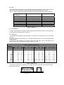
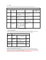
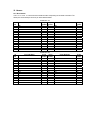
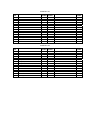
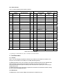
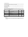
3DK1657
USER MANUAL
FOR H8SX/1657 ON-CHIP FLASH
MICROCONTROLLER
Warning
Check the silkscreen around the power jack (J9) for the minimum and maximum voltage input levels for this 3DK.
Always use a centre positive supply for this board.
DO NOT USE AN E6000 POWER SUPPLY with this 3DK
Preface
Cautions
1.
This document may be, wholly or partially, subject to change without notice.
2.
All rights reserved. No one is permitted to reproduce or duplicate, in any form, a part or this
entire document without Renesas Technology Europe Limited's written permission.
Trademarks
General
All brand or product names used in this manual are trademarks or registered trademarks of their
respective companies or organisations.
Document Information
Product Code:
D005463_11
Version:
1
Date:
23/11/2004
Copyright © Renesas Technology Europe Ltd. 2004. All rights reserved.
Website:
http://www.eu.renesas.com/
TABLE OF CONTENTS
TABLE OF CONTENTS .......................................................................................................................................................3
1.
POWER REQUIREMENTS ..........................................................................................................................................4
2.
POWER – UP BEHAVIOUR ........................................................................................................................................4
3.
PURPOSE ...............................................................................................................................................................4
4.
BOARD LAYOUT ......................................................................................................................................................4
5.
BLOCK DIAGRAM ....................................................................................................................................................5
6.
USER CIRCUITRY ....................................................................................................................................................5
6.1. SWITCHES...........................................................................................................................................................5
6.2. LEDS ....................................................................................................................................................................6
6.3. POTENTIOMETER...............................................................................................................................................6
6.4. SERIAL PORT ......................................................................................................................................................6
6.5. JUMPERS.............................................................................................................................................................7
7.
OSCILLATOR SOURCES ...........................................................................................................................................7
8.
MODES ...................................................................................................................................................................8
8.1. BOOT MODE........................................................................................................................................................8
8.2. USER MODE ........................................................................................................................................................8
9.
PROGRAMMING METHODS .......................................................................................................................................8
9.1. PORT PROGRAMMING.......................................................................................................................................9
9.2. FDM HEADER ......................................................................................................................................................9
9.3. E7 HEADER..........................................................................................................................................................9
9.4. OFF-BOARD PROGRAMMING............................................................................................................................9
10. HEADERS .............................................................................................................................................................10
10.1. MICON HEADERS..............................................................................................................................................10
10.2. GENERIC HEADERS .........................................................................................................................................12
11. CODE DEVELOPMENT ............................................................................................................................................12
11.1. OVERVIEW ........................................................................................................................................................12
11.2. MODE SUPPORT...............................................................................................................................................12
11.3. BREAKPOINT SUPPORT ..................................................................................................................................13
11.4. CODE LOCATED IN RAM..................................................................................................................................13
11.5. HMON CODE SIZE.............................................................................................................................................13
11.6. MEMORY MAP...................................................................................................................................................13
11.7. BAUD RATE SETTING.......................................................................................................................................14
11.8. INTERRUPT MASK SECTIONS.........................................................................................................................15
11.9. ADDITIONAL INFORMATION ............................................................................................................................15
1. POWER REQUIREMENTS
All 3DK boards are centre positive with a 2.5mm barrel power jack.
The diode, D1 provides reverse polarity protection.
A 9V, centre positive supply is suitable for use with this board.
Warning
Check the silkscreen around the power jack (J9) for the minimum and maximum voltage input levels for this 3DK.
The 3DK is neither under nor over voltage protected.
Always use a centre positive supply for this board.
DO NOT USE AN E6000 POWER SUPPLY with this 3DK
2. POWER – UP BEHAVIOUR
The 3DK board has code pre-programmed into the Renesas microcontroller. On powering up the board, pressing
switch 2 will cause the red user LEDs to flash. Switches 2 and 3 as well as the potentiometer can be used to
modify the LED flashing pattern.
3. PURPOSE
This 3DK board is an evaluation tool for Renesas microcontrollers.
Features include:
a. Renesas Microcontroller Programming
b. User Code Debugging
c. User Circuitry such as Switches, LEDs and potentiometer(s)
d. User or Base Board Connectivity
The 3DK board contains all the circuitry required for microcontroller operation.
4. BOARD LAYOUT
The following diagram shows top layer component layout of the board.
Note: The diagram below is for illustrative purposes and does not accurately reflect the 3DK detailed in this
manual.
RES
J3
DEBUG
U1
OFF
USER
SWITCHES
ON
MICON
HEADER
J2
MICON
HEADER
J3
MCU_SEL
FLASH
HEADER
J4
19-WAY
GENERIC
HEADER J5
MCU
SELECT
SWITCH
SW3
SERIAL
PORT
CLED8
CLED7
Renesas
Microcontroller
J8
CLED6
SW2
CLED5
CLED4
BOOTJ7
USER
LEDS
J12
CLED3
J2
POWER
JACK
SW1/BOOT
J5
J6
CLED2
J9
CLED1
BOOT LED
J1
BOOT
MICON
SINGLE TURN
HEADER POTENTIOMETER
J4
MICON
HEADER
J1
DEBUG
HEADER
20-WAY
GENERIC
HEADER
J6
RS232
Transceiver
IC
C 2004 Renesas Technology Europe LTD.
BOOT LATCH
U2
HC74 dual
D-type logic
U5
Crystal / Oscillator /
Resonator Components
/ Footprints
U6
5. BLOCK DIAGRAM
Diagram x.1 is representative of the 3DK components and their connectivity.
Power Jack & Regulator IC
Generic Headers
Microcontroller
Boot mode pins
Flash/Boot Header
Micon Headers
RESET pin
Boot Circuitry
RESn
D-type latch
Serial Connector
BOOT & BOOTn signals
IRQ/wakeup pin
IRQ/wakeup pin
Debug Header
SW2
Potentiometer
RES
SW3
BOOT
SWITCHES
LEDs
8 Red LEDS
1 Green
LED
6. USER CIRCUITRY
6.1. SWITCHES
There are four switches located on the 3DK. These are:
Switch
SW1/BOOT
Function
This switch is used in conjunction with the RES switch to place the
device in BOOT mode.
SW2
This switch is connected via a 0R link to an IRQ line capable of
waking up the microcontroller device from sleep mode.
SW3
This switch is connected via a 0R link to another IRQ line capable of
waking up the microcontroller device from sleep mode.
RES
This switch when pressed resets the 3DK microcontroller.
NB. Refer to schematic for detailed connectivity information.
Microcontroller
IRQ0-A, Pin 72
(Port 1, pin 0)
IRQ1-A , Pin73
(Port 1, pin 1)
IRQ2-A, Pin 74
(Port 1, pin 2)
RESn
Regulator
IC
6.2. LEDS
There are nine LEDs on the 3DK board. The green BOOT LED indicates the device is in boot mode when lit. The
eight red LEDs are connected to an IO port and will light when their corresponding port pin is set low.
Table 6-1, below, shows the LED pin references and their corresponding microcontroller port pin connections.
LED Reference (As shown
on silkscreen)
Microcontroller Port Pin function
CLED1
CLED2
CLED3
CLED4
CLED5
CLED6
CLED7
CLED8
Microcontroller Pin Number
PH0
PH1
PH2
PH3
PH4
PH5
PH6
PH7
53
54
55
56
58
59
60
61
Table 6-1:LED Port
6.3. POTENTIOMETER
A single turn potentiometer is connected to AN0 of the microcontroller. This may be used to vary the input analog
voltage value to this pin between AVCC and Ground.
6.4. SERIAL PORT
The microcontroller programming serial port (SCI4) is connected to the D–type connector J8 via an RS232
transceiver.
A secondary microcontroller serial port (SCI1) is connected to generic header, J6 via the second channel of the
RS232 transceiver.
The serial baud rates supported by this 3DK are shown below. Note: these values are calculated from the
frequency value of the main oscillating source fitted by default on this 3DK.
Baud Rate Register Settings for Serial Communication Rates
Values are calculated for 29.4984MHz clock
SMR Setting:
Comm. Baud
0
1
2
3
BRR
setting
Actual
Rate
ERR
(%)
BRR
setting
Actual
Rate
ERR
(%)
BRR
setting
Actual
Rate
ERR
(%)
BRR
setting
Actual
Rate
ERR (%)
110 invalid
invalid
invalid
300 invalid
invalid
invalid
invalid
invalid
invalid
invalid
invalid
invalid
64
111
0.70
invalid
invalid
invalid
95
300
0.00
23
300
0.00
1200 invalid
invalid
invalid
95
1200
0.00
23
1200
0.00
5
1200
0.00
2400
0.00
47
2400
0.00
11
2400
0.00
2
2400
0.00
2400
191
4800
95
4800
0.00
23
4800
0.00
5
4800
0.00
1
3600
-25.00
9600
47
9600
0.00
11
9600
0.00
2
9600
0.00
invalid
invalid
invalid
19200
23
19200
0.00
5
19200
0.00
1
14400
-25.00
invalid
invalid
invalid
38400
11
38400
0.00
2
38400
0.00
invalid
invalid
invalid
invalid
invalid
invalid
57600
7
57600
0.00
1
57600
0.00
invalid
invalid
invalid
invalid
invalid
invalid
115200
3
115200
0.00
0
115200
0.00
invalid
invalid
invalid
invalid
invalid
invalid
Table 6-2 : BRR Settings
This serial port may be used as a debugging communication port or as a normal serial communication port when
the device is in user mode.
5
4
9
3
8
2
7
1
6
Female serial
connector showing
pin numbering
Power Jack
6.5. JUMPERS
Table 6-3 below describes the function of the 2-Pin jumpers contained on this 3DK board.
2-Pin Jumper Settings
Reference
Jumper
Function
Fitted
Alternative (Removed)
Footprint for jumper
only/Jumper pins
fitted
J10
RX Disable
PRXD from the RS232
device to U1 is enabled.
This enables serial port
communication.
Disabled. This allows the
FDM to program the
microcontroller
Jumper pins fitted
J11
UVCC power
Measurement
Bypasses R11, a 1206 0R
resistor,
for
current
measurement
R11 must be fitted to
power UVCC
Footprint only
J13
User Boot
A transition to user mode is
made once a boot switch
sequence is performed by
the user
A transition to boot mode
is made once a boot
switch
sequence
is
performed by the user
J14
Regulator
Bypass
Bypasses the regulator;
power to board is taken
directly from external
supply (additionally R87
must be fitted and R85
removed)
Board supply is taken via
regulator
Table 6-4: 2-Pin jumpers
7. OSCILLATOR SOURCES
A ceramic resonator is fitted on the 3DK and used to supply the main clock input to the Renesas microcontroller.
Table 7-1 details the oscillators that are fitted and alternative footprints provided on this 3DK:
Component
Resonator
(X1)
Crystal (X2)
Crystal (X3)
Subclock
Details
Footprint Only
&/or fitted*
14.7458MHz
Footprint Only
&/or fitted*
14.745MHz
Footprint only
14.7456MHz recommended
value (HC/49U package)
115200
(4.1mm x 4.7mm package)
115200
(low profile package 5mm x
7mm x 1.3mm)
115200
None
Table 7-1: Oscillators / Resonators
* Either X1 or X2 will be fitted on this board.
Warning: When replacing the default oscillator with that of another frequency, the FDT programming kernels
supplied will need rebuilding. The supplied HMON debugging monitor will not function. The user is responsible for
code written to support operating speeds other than the default. See the HMON user manual for details of making
the appropriate modifications in the code to accommodate different operating frequencies.
8. MODES
The 3DK supports User mode, Boot mode and User Boot mode. User mode may be used to run and debug user
code, while Boot mode may only be used to program the Renesas microcontroller with program code. User Boot
mode can only be used to program the User Mat (the main area, 768Kbytes, of Flash ROM on the device). It does
not support programming of the user boot area. User Boot mode is used to run a user bootloader program stored
in the user boot MAT (the smaller area, 8Kbytes, of Flash ROM). To program the user boot MAT, the device must
be in Boot mode. Further details of programming the MATs are available in the H8SX/1657 hardware manual.
To enter boot mode, press and hold the boot button so that the mode pins are held in their boot states while reset
is pressed and released. Then release the boot button. The BOOT LED will be illuminated to indicate that the
microcontroller is in boot mode.
8.1. BOOT MODE
The boot mode settings for this 3DK are shown in Table 8-1 below:
MD0
1
1
MD1
1
0
MD2
1
0
LSI State after Reset End
User Mode
Boot Mode
Table 8-1: Mode pin settings
8.2. USER BOOT MODE
A Note on Mats:
The H8SX/1657 possesses two distinct areas of Flash, User MAT (768KByte) and User Boot MAT (8KByte). The
User Boot MAT is a separate area of FLASH from User MAT, intended to hold user boot code.
A custom boot stub could be programmed into User Boot MAT which allows programming and erasing of the User
MAT in User Mode, without erasing the contents of the User Boot MAT. Once User Boot Mode is entered, code
contained in the User Boot MAT is executed. This differs to Boot mode, as Boot mode erases all User MAT and
requires an auto-baud on a fixed SCI port to be performed. The existence of the user boot Mat therefore allows an
alternative communications port to be used for further code download to the User MAT. Programming of the user
boot mat may only be performed in boot mode.
The user may place the H8SX/1657 device provided on a 3DK1657 board in user boot mode by fitting jumper J13.
The Boot procedure must then be performed for entry into user boot mode. The Boot LED should light, suggesting
a transition to user boot mode.
The user boot mode settings for this 3DK are shown in Table 8-1 below:
MD0
0
MD1
1
MD2
0
LSI State after Reset End
User Boot Mode
Table 8-2: Mode pin settings
8.3. USER MODE
For the device to enter User Mode, reset must be held active while the microcontroller mode pins are held in
states specified for User Mode operation. 100K pull up and pull down resistors are used to set the pin states
during reset.
The H8SX/1657 supports 4 user modes. The memory map in all of these modes is 16Mbyte in size. The default
user mode for 3DK1657 is 7.
9. PROGRAMMING METHODS
All of the Flash ROM on the device (i.e. both MATs) can be programmed when the device is in Boot mode. Once
in boot mode, the bootloader program pre-programmed into the microcontroller executes and attempts a
connection with a host (for example, a PC). The host, on establishing a connection with the microcontroller, may
then transmit program data to the microcontroller via the appropriate programming port.
Table 9-1below shows the programming port for this Renesas Microcontroller and its associated pins
Programming Port Table – Programming port pins and their 3DK signal names
SCI4
TXD4, PIN 89
RXD4, PIN 90
SCK4, PIN 91
3DK Signal Name
PTXD
PRXD
PSCK
Table 9-1: Serial Port Boot Channel
9.1. PORT PROGRAMMING
The microcontroller must enter boot mode for programming, and the programming port must be connected to a
host for program download. To execute the boot transition, and allow programs to download to the microcontroller,
the user must perform the following procedure:
1.
2.
3.
4.
Connect a 1:1 serial cable between the host PC and the 3DK board
Depress the RESET switch and keep this held down
Depress the BOOT switch once, and release
Release the RESET switch
9.2. FDM HEADER
The Renesas FDM (Flash Debug Module) is a USB based programming tool for control and programming of
Renesas microcontrollers, available separately from Renesas. The 3DK serial programming signals PTXD, PRXD,
PSCK and the microcontroller mode pins as well as the microcontroller reset signal are all connected to this
header. The FDM, when connected to the Flash Programming header, is therefore capable of forcing the
microcontroller into boot mode, programming and resetting the 3DK microcontroller.
To utilise this header the user must make the following changes to the board configuration.
1.
Jumper link J10 must be removed.
9.3. E7, E10A AND E10T HEADERS
This device does not currently support any of the E7, E10A or E10T programming tools.
9.4. OFF-BOARD PROGRAMMING
All 3DKs are capable of programming an alternative microcontroller on a secondary board. The user is responsible
for providing this second board containing the alternative microcontroller, its supporting circuitry and an FDM or
FoUSB header for the microcontroller.
To program the alternative microcontroller, the user should perform the following steps
•
•
Connect a cable between the 3DK programming header and that located on the secondary board.
Slide switch MCU_SEL to the off-board programming position (OFF). This holds the microcontroller on
the 3DK in reset, preventing it from being programmed.
10. HEADERS
10.1. MICON HEADERS
Table 10-1 to Table 10-4 shows the micon headers and their corresponding microcontroller connections. The
header pins connect directly to the micon pin unless otherwise stated.
Table 10-1: J1
J1
Pin
1
3
5
7
9
11
13
15
17
19
21
23
25
27
29
Circuit Net Name
PB1
PB3
PF7
PF5
PF3
PF2
PF0
PE6
GROUND
BOARD_VCC
PE2
PE0
PD6
PD5
PD3
U1 pin
number
1
3
5
7
9
11
13
15
17
19
21
23
25
27
29
J1 pin
number
2
4
6
8
10
12
14
16
18
20
22
24
26
28
30
Circuit Net Name
PB2
MD2
PF6
PF4
GROUND
PF1
PE7
PE5
PE4
PE3
PE1
PD7
GROUND
PD4
PD2
U1 pin
number
2
4
6
8
10
12
14
16
18
20
22
24
26
28
30
Table 10-2: J2
J2
Pin
1
3
5
7
9
11
13
15
17
19
21
23
25
27
29
Circuit Net Name
PD1
EMLE
P21
P23
RXD1
P27
P30
P31
P33
P35
P37
PH0
PH2
GROUND
PH5
U1 pin
number
31
33
35
37
39
41
43
45
47
49
51
53
55
57
59
J2 pin
number
2
4
6
8
10
12
14
16
18
20
22
24
26
28
30
Circuit Net Name
PD0
P20
P22
P24
TXD1
GROUND
BOARD_VCC
P32
P34
P36
NMI
PH1
PH3
PH4
PH6
U1 pin
number
32
34
36
38
40
42
44
46
48
50
52
54
56
58
60
Table 10-3: J3
J3
Pin
1
3
5
7
9
11
13
15
17
19
21
23
25
27
29
Circuit Net Name
PH7
PI0
PI2
GROUND
PI5
PI7
P11
P13
RESn
P14
WDTOVFn
XTAL
BOARD_VCC
P17
PTXD
U1 pin
number
61
63
65
67
69
71
73
75
77
79
81
83
85
87
89
J3 pin
number
2
4
6
8
10
12
14
16
18
20
22
24
26
28
30
Circuit Net Name
Board_Vcc
PI1
PI3
PI4
PI6
P10
P12
GROUND
NC (Vcl Pin)
P15
GROUND
EXTAL
P16
STBYn
P61
U1 pin
number
62
64
66
68
70
72
74
76
78
80
82
84
86
88
90
Table 10-4: J4
J1
Pin
1
3
5
7
9
11
13
15
17
19
21
23
25
27
29
Circuit Net Name
P62
P63
P64
MD0
P51
CON_AVCC
CON_AVSS
CON_VREF
P56
MD1
PA1
PA3
PA5
GROUND
BOARD_VCC
U1 pin
number
91
93
95
97
99
101
103
105
107
109
111
113
115
117
119
J1 pin
number
2
4
6
8
10
12
14
16
18
20
22
24
26
28
30
Circuit Net Name
NC (PLL Pin)
NC (PLL Pin)
P65
P50
P52
P53
P54
P55
P57
PA0
PA2
PA4
PA6
PA7
PB0
U1 pin
number
92
94
96
98
100
102
104
106
108
110
112
114
116
118
120
10.2. GENERIC HEADERS
Table 10-5below shows the generic header connections
19 way generic Header
Pin
Generic
Number Header Name
1
Supply
3DK Signal Name
20 way generic Header
Supply
Micon
Pin
N\A
Generic Header
Pin
Name
Number
1
IOPORT_TXD
3DK Signal
Name
IOPORT_TXD
Micon
Pin
N\A
2
Xin
CON_EXTAL
N\A
2
IOPORT_RXD
IOPORT_RXD
N\A
3
Vcc
Board_VCC
N\A
3
IOPORT_T1
IOPORT_T1
48
4
Vss
Ground
N\A
4
IOPORT_T2
IOPORT_T2
49
5
Vcc
Board_VCC
N\A
5
IOPORT_T3
IOPORT_T3
50
6
Vss
Ground
N\A
6
IOPORT_T4
IOPORT_T4
51
7
AVcc
AVCC
101
7
IOPORT_U
NC
N\A
8
AVss
AVSS
103
8
IOPORT_V
NC
N\A
9
Vref
VREF
105
9
IOPORT_W
NC
N\A
10
AN0
PIN98
98
10
IOPORT_0
IOPORT_0
53
11
AN1
PIN99
99
11
IOPORT_1
IOPORT_1
54
12
AN2
PIN100
100
12
IOPORT_2
IOPORT_2
55
13
AN3
PIN102
102
13
IOPORT_3
IOPORT_3
56
14
DAC0
PIN107
107
14
IOPORT_4
IOPORT_4
58
15
DAC1
PIN108
108
15
IOPORT_5
IOPORT_5
59
16
SCL
N\A
N\A
16
IOPORT_6
IOPORT_6
60
17
SDA
N\A
N\A
17
IOPORT_7
IOPORT_7
61
18
CTX
N\A
N\A
18
/Reset
RESn
77
19
CRX
N\A
N\A
19
IOPORT_INT
NMIn
52
20
VSS
GROUND
N\A
Table 10-5: Generic Headers
* Connected via a DNF 0R Link, refer to schematic for further details.
11. CODE DEVELOPMENT
11.1. OVERVIEW
Note: For all code debugging using Renesas software tools, the 3DK board must either be connected to a PC
serial port via a serial cable or a PC USB port via an FDM (Flash Debug Module).
The HMON embedded monitor code is modified for each specific 3DK Renesas Microcontroller. HMON enables
HEW to establish a serial connection to the 3DK microcontroller, and control code execution on the
microcontroller. Breakpoints may be set in memory to halt code execution at a specific point. The code may be
started from this point.
The HMON embedded monitor code must be compiled with user software and downloaded to the 3DK, allowing
the users’ code to be debugged within HEW.
11.2. MODE SUPPORT
The HMON library is built to support 16Mbyte advanced Mode for the H8SX family only.
11.3. BREAKPOINT SUPPORT
The device has no break controller. No breakpoints can be located in ROM code. However, code located in RAM
may have multiple breakpoints limited only by the size of the On-Chip RAM.
11.4. CODE LOCATED IN RAM
Double clicking in the breakpoint column in the code sets the breakpoint. Breakpoints will remain unless they are
double clicked to remove them.
11.5. HMON CODE SIZE
HMON is built along with the debug code. Certain elements of the HMON code must remain at a fixed location in
memory. The following table details the HMON components and their size and location in memory. For more
information, refer to the map file when building code.
Section
Description
Start Location
Size
(H’bytes)
RESET_VECTOR
HMON Reset Vector (Vector 0)
Required for Startup of HMON
HMON Serial Port Vectors (Vector 160, 161, 162, 163)
Used by HMON when EDK is configured to connect to the
default serial port.
HMON Code
HMON Constant Data
HMON Uninitialised data
H’ 0000 0000
4
H’0000 0280
F
H’0000 3000
H’0000 5730
H’00FF 6494
2730
134
21F
FDT Kernel.
This is at a fixed location and must not be moved. Should
the kernel need to be moved it must be re-compiled.
Pointer used by HMON to point to the start of user code.
H’0000 1000
E64
H’0000 0800
4
SCI_VECTORS
PHMON
CHMON
BHMON
UGenU
CUser_Vectors
11.6. MEMORY MAP
The memory map shown in this section visually describes the locations of program code sections related
to HMON, the FDT kernels and the supporting code within the ROM/RAM memory areas of the
microcontroller.
H'0000
Vectors
H'0800
H'0803
H'1000
RESET Vector
H'0000
H'0003
SCI Vectors
H'0280
H'028B
CUser_Vectors
UGenU FDT Kernel
H'1E63
H'3000
PHMON
CHMON
H'5863
On-Chip FLASH
ROM
H'BFFFF
H'FF6000
On-Chip RAM
H'FF6494
BHMON
H'FF66B2
H'FFBE00
Stack
H'FFBFFF
H'FFFB80
H'FFFFFF
Internal I/O
REGISTERS
11.7. BAUD RATE SETTING
HMON is initially set to connect at 115200 Baud. The value set in the baud rate register for the microcontroller
must be altered if the user wishes to change either the serial communication baud rate of the serial port or the
operating frequency of the microcontroller. This value is held in the HMONserialconfiguser.c file, as
SCI_CFG_BRR (see the Serial Port section for baud rate register setting values). The project must be re-built and
the resulting code downloaded to the microcontroller once the BRR value is changed. Please refer to the HMON
User Manual for further information.
11.8. INTERRUPT MASK SECTIONS
HMON has an interrupt priority of 6. The serial port has an interrupt priority of 7. Modules using interrupts should
be set to lower than this value (6 or below), so that serial communications and debugging capability is maintained.
11.9. ADDITIONAL INFORMATION
For details on how to use High-performance Embedded Workshop (HEW), with HMON, refer to the HEW manual
available on the CD or from the web site.
For information about the H8SX/1657 series microcontrollers refer to the H8SX/1657 Series Hardware Manual
For information about the H8SX/1657 assembly language, refer to the H8 Series Programming Manual
Further information available for this product can be found on the Renesas web site at:
http://www.eu.renesas.com/tools
General information on Renesas Microcontrollers can be found at the following URLs.
Global:
http://www.renesas.com/