1
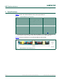
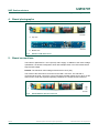
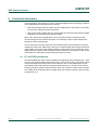
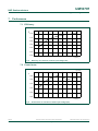
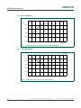
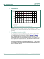
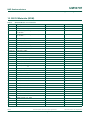
UM10797 SSL5015DB1201 120 V 18 W low THD low ripple dual stage converter Rev. 1 — 28 May 2014 User manual Document information Info Content Keywords SSL5015DB1201, non-dimmable, LED driver, boost buck dual stage converter, TLED, Low Total Harmonic Distortion (LTHD), Low Ripple (LR) Abstract This document describes the operation of a 120 V 18 W non-dimmable LED driver featuring the SSL5015 using a boost/buck dual stage topology. The SSL5015DB1201 demo board has a form factor that is compatible with the base of a T8 LED lamp fitting used in Solid State Lighting (SSL) applications UM10797 NXP Semiconductors SSL5015DB1201 120 V 18 W low THD low ripple dual stage converter Revision history Rev Date Description v.1 20140528 first issue Contact information For more information, please visit: http://www.nxp.com For sales office addresses, please send an email to: [email protected] UM10797 User manual All information provided in this document is subject to legal disclaimers. Rev. 1 — 28 May 2014 © NXP Semiconductors N.V. 2014. All rights reserved. 2 of 19 UM10797 NXP Semiconductors SSL5015DB1201 120 V 18 W low THD low ripple dual stage converter 1. Introduction WARNING Lethal voltage and fire ignition hazard The non-insulated high voltages that are present when operating this product, constitute a risk of electric shock, personal injury, death and/or ignition of fire. This product is intended for evaluation purposes only. It shall be operated in a designated test area by personnel qualified according to local requirements and labor laws to work with non-insulated mains voltages and high-voltage circuits. This product shall never be operated unattended. This document describes the operation of a 120 V 18 W non-dimmable LED driver featuring the SSL5015. The SSL5015DB1201 demo board has a form factor that is T8 LED lamp compatible. The boost buck dual stage converter topology provides a simple and efficient solution that achieves low input THD and low output ripple with a small output buffer capacitor. The total input power (VA) of the board is 18.6 W at 120 V/155 mA. The demo board is designed to drive an LED load, delivering an output power of 15.6 W at 60 V/260 mA. The power factor (PF) is 0.96 which gives an actual input power of 0.96 18.6 W = 17.86 W. The resulting efficiency is > 87 %. The demo board complies with EMI and safety regulations. Figure 2 shows the SSL5015DB1201 demo board dimensions. The design and the components used ensure that the board fits into a T8 lamp base. 2. Safety warning The SSL5015DB1201 demo board input is connected to the 120 V mains. Avoid touching the board while it is connected to the mains voltage and when it is in operation. An isolated housing is obligatory when used in uncontrolled, non-laboratory environments. Galvanic isolation from the mains phase using a fixed or variable transformer is always recommended. Figure 1 shows the symbols that identify the isolated and non-isolated devices. 019aab174 019aab173 a. Isolated Fig 1. UM10797 User manual b. Not isolated Variable transformer (variac) isolation symbols All information provided in this document is subject to legal disclaimers. Rev. 1 — 28 May 2014 © NXP Semiconductors N.V. 2014. All rights reserved. 3 of 19 UM10797 NXP Semiconductors SSL5015DB1201 120 V 18 W low THD low ripple dual stage converter 3. Specifications Table 1 contains the SSL5015DB1201 demo board specifications. Table 1. SSL5015DB1201 specifications Symbol Parameter Value Vmains AC mains supply voltage 120 V VLED output voltage 60 V ILED output current 260 mA ILED/VLED output voltage rejection 3 mA/15 V efficiency > 87 % PF Power Factor 0.96 THD Total Harmonic Distortion < 30 % Toper operating temperature -40 C to +100 C fsw switching frequency 70 kHz Io(ripple) ripple output current 7 % (16 mA)[1] [1] The ripple current can be reduced by using a larger bus capacitor or output capacitor. For example, with a 100 F capacitor at output, the ripple current can be reduced around 5 % at rated voltage input. Figure 2 shows the dimensions of the SSL5015DB1201 demo board. Fig 2. UM10797 User manual SSL5015DB1201 board dimensions All information provided in this document is subject to legal disclaimers. Rev. 1 — 28 May 2014 © NXP Semiconductors N.V. 2014. All rights reserved. 4 of 19 UM10797 NXP Semiconductors SSL5015DB1201 120 V 18 W low THD low ripple dual stage converter 4. Board photographs a. Top view b. Bottom view Fig 3. SSL5015 18 W demo board 5. Board connections The board is optimized for a 120 V (60 Hz) mains supply. In addition to the mains voltage optimization, the board is designed to work with multiple LEDs or an LED module with a high forward voltage. Remark: The maximum rated voltage of the board is 132 V (AC). The anode of the LED load is connected to the LED+ connector. The cathode is connected to the LED connector. Use an LED string forward voltage of up to 60 V on this demo board. Under the expected operating conditions, the output current is 260 mA. Fig 4. UM10797 User manual SSL5015DB1201 board connections All information provided in this document is subject to legal disclaimers. Rev. 1 — 28 May 2014 © NXP Semiconductors N.V. 2014. All rights reserved. 5 of 19 UM10797 NXP Semiconductors SSL5015DB1201 120 V 18 W low THD low ripple dual stage converter 6. Functional description In this application, the SSL5015 is used in a double stage boost-buck topology instead of in the designated buck topology for two reasons: • With a boost stage at the input side, the input capacitance of the system can be kept to a minimum, allowing a high power factor. • With a buck stage at output side, the output ripple can be low because the bus voltage supplied by the preceding boost stage is stable. When using the boost-buck application, only one switching FET is required to draw current through the boost and buck stages. The switching current in both stages flows through the same switching FET. The IC senses the current through the sense resistor (R6; R13) and switches off when it reaches the peak value. Most of the current in the sense resistor flows mainly through the output LEDs. The boost current follows a different return path through resistor R8. It only slightly effects the peak current through the sense resistors. So, the output current can be calculated in the same way as with an SSL5015 buck converter. 6.1 PF and THD performance The SSL5015DB1201 demo board is designed for high power factor operation (PF > 0.95 at 120 V (AC)) and low THD performance (THD < 30 % at 120 V (AC)). The return current of the boost stage shapes the input current waveform. So, PF and THD depend on the ratio between the boost inductor (L2) and the buck inductor (L3). A ratio of L2/L3 that is smaller generally provides a higher PF and a lower THD. However, it also causes a higher bus voltage which challenges the IC voltage rating. So, keep the inductor value accuracy of both within 5 %. UM10797 User manual All information provided in this document is subject to legal disclaimers. Rev. 1 — 28 May 2014 © NXP Semiconductors N.V. 2014. All rights reserved. 6 of 19 UM10797 NXP Semiconductors SSL5015DB1201 120 V 18 W low THD low ripple dual stage converter 7. Performance 7.1 Efficiency Ș DDD Fig 5. 9L9$& Efficiency as a function of mains input voltage (AC) 7.2 Power factor DDD 3) Fig 6. UM10797 User manual 9L9$& Power factor as a function of mains input voltage (AC) All information provided in this document is subject to legal disclaimers. Rev. 1 — 28 May 2014 © NXP Semiconductors N.V. 2014. All rights reserved. 7 of 19 UM10797 NXP Semiconductors SSL5015DB1201 120 V 18 W low THD low ripple dual stage converter 7.3 Line regulation DDD ,R $ Fig 7. 9L9$& Output current as a function of mains input voltage (AC) 7.4 Load regulation DDD ,R $ Fig 8. UM10797 User manual 9R9 Output current as a function of output voltage All information provided in this document is subject to legal disclaimers. Rev. 1 — 28 May 2014 © NXP Semiconductors N.V. 2014. All rights reserved. 8 of 19 UM10797 NXP Semiconductors SSL5015DB1201 120 V 18 W low THD low ripple dual stage converter 7.5 Ripple and THD DDD 5LSSOH7+' 9L9 (1) Output ripple (2) Input THD Fig 9. Output ripple and input THD as a function of input voltage Remark: To increase the bus voltage, reduce the L2 (boost inductance) / L3 (buck inductance) ratio. The reduction ensures better output ripple performance in 100 V (AC) applications. 7.6 ElectroMagnetic Interference (EMI) EMI was measured according to the EN55015 standard. The SSL5015DB1201 demo board complies with the requirements of the standard (see Figure 10 to Figure 12). The SSL5015 series operates as a boundary conduction mode converter. A special feature, called valley detection, is an integrated part of the SSL5015 series circuitry. Dedicated built-in circuitry connected to the DRAIN pin senses when the voltage on the drain of the switch has reached its lowest value. This feature reduces switching losses. It also greatly benefits the EMI performance of the LED driver. The switching point follows immediately after the buck stage. Both inductors in this circuit are sensitive to other magnets. So, to optimize the EMI performance, an outer shielding has been added on both inductors. This shielding ensures better EMI performance over frequency ranges are > 300 kHz. UM10797 User manual All information provided in this document is subject to legal disclaimers. Rev. 1 — 28 May 2014 © NXP Semiconductors N.V. 2014. All rights reserved. 9 of 19 UM10797 NXP Semiconductors SSL5015DB1201 120 V 18 W low THD low ripple dual stage converter Fig 10. EMI performance - Conduction Emission (CE) - L-phase Fig 11. EMI performance - Conduction Emission (CE) - N-phase UM10797 User manual All information provided in this document is subject to legal disclaimers. Rev. 1 — 28 May 2014 © NXP Semiconductors N.V. 2014. All rights reserved. 10 of 19 UM10797 NXP Semiconductors SSL5015DB1201 120 V 18 W low THD low ripple dual stage converter Fig 12. EMI performance - Radiation Emission (SE) 8. Protections 8.1 Bus OverVoltage Protection (OVP) Additional protections are embedded to provide input overvoltage protection (R2; R3; R4; R5; ZD1; Q2) for the boost stage (see Figure 13). The input overvoltage protection switches off the IC when the bus voltage on C1 is too high. If the bus voltage exceeds the OVP set point (= 282 V), it pulls down the VCC voltage. The limit can be tuned by adjusting the ratio between R2, R3 and R4. The limit must be tuned below the maximum voltage rating of the IC. The protection automatically restarts when the input voltage is reduced. 8 5 Nȍ +9 6285&( 5 Nȍ 6285&( 5 9&& ȍ =' 4 %& 9 5 Nȍ 5 Nȍ & ) ,& '5$,1 *1' '9'7 17& & ) 9 DDD Fig 13. Bus overvoltage protection UM10797 User manual All information provided in this document is subject to legal disclaimers. Rev. 1 — 28 May 2014 © NXP Semiconductors N.V. 2014. All rights reserved. 11 of 19 UM10797 NXP Semiconductors SSL5015DB1201 120 V 18 W low THD low ripple dual stage converter 8.2 Boost OverCurrent Protection (OCP) If the boost peak current exceeds Vth / R8 (Vth is the threshold voltage of Q3 and D7; see Figure 14), the overcurrent protection in the boost stage (R8; Q3; D7) pulls down the VCC voltage. This circuit is not active under typical conditions. However, the circuit is required because the IC cannot detect boost stage peak currents in this topology. 8 +9 6285&( 6285&( 5 ȍ 4 (& 9&& & ) 9 ,& *1' '5$,1 *1' '9'7 17& ' 1 5 ȍ 5 ȍ 5 ȍ DDD Fig 14. Boost overcurrent protection 8.3 Output OverVoltage Protection (OVP) The voltage rating of the output capacitor can be limited to 100 V. However, extra components (ZD2; Q4; R11; R12) are then required to protect the output capacitor against possible high voltages (see Figure 15). The circuit provides a low impedance path if the output voltage exceeds the breakdown voltage of Zener diode ZD2. The IC detects this low impedance as a short at the output and activates the output short protection (latched protection). /(' =' 9 5 Nȍ 4 %7' 5 ȍ & ) 9 /(' DDD Fig 15. Output overvoltage protection UM10797 User manual All information provided in this document is subject to legal disclaimers. Rev. 1 — 28 May 2014 © NXP Semiconductors N.V. 2014. All rights reserved. 12 of 19 xxxxxxxxxxxxxxxxxxxxx xxxxxxxxxxxxxxxxxxxxxxxxxx xxxxxxx x x x xxxxxxxxxxxxxxxxxxxxxxxxxxxxxx xxxxxxxxxxxxxxxxxxx xx xx xxxxx xxxxxxxxxxxxxxxxxxxxxxxxxxx xxxxxxxxxxxxxxxxxxx xxxxxx xxxxxxxxxxxxxxxxxxxxxxxxxxxxxxxxxxx xxxxxxxxxxxx x x xxxxxxxxxxxxxxxxxxxxx xxxxxxxxxxxxxxxxxxxxxxxxxxxxxx xxxxx xxxxxxxxxxxxxxxxxxxxxxxxxxxxxxxxxxxxxxxxxxxxxxxxxx xxxxxxxx xxxxxxxxxxxxxxxxxxxxxxxxx xxxxxxxxxxxxxxxxxxxx xxx NXP Semiconductors UM10797 User manual 9. Schematic ' QP ) / 9L 9$& ' / + / P+ &; Q) 029 .' 1 /(' 5 %' 0%6 (6- Nȍ / / P+ + 6285&( 6285&( 5 ȍ =' ȍ ȍ ,& *1' 5 Nȍ 4 %& 4 %7' & ) 9 9R 9 OR P$ & S) 9 5 Nȍ / '5$,1 P+ *1' 5 ȍ & ) 9 /(' & Q) 9 '9'7 17& 17& QP 4 %& 9 5 Nȍ 9&& & ) 9 5 8 +9 5 Nȍ 5 & ) ' 1 5 ' 30(*%(3 ȍ 5 ȍ 5 ȍ Fig 16. 120 V 18 W TLED LTHD_LR dual stage converter with SSL5015DB1201 demo board schematic UM10797 13 of 19 © NXP Semiconductors N.V. 2014. All rights reserved. DDD SSL5015DB1201 120 V 18 W low THD low ripple dual stage converter Rev. 1 — 28 May 2014 All information provided in this document is subject to legal disclaimers. 5 Nȍ =' 9 ' (6- (6- & Q) 9 & Q) 9 ' UM10797 NXP Semiconductors SSL5015DB1201 120 V 18 W low THD low ripple dual stage converter 10. Bill Of Materials (BOM) Table 2. SSL5015DB1201 bill of materials Reference Description and values Part number Manufacturer BD1 bridge rectifier MB6S - CX1 X-capacitor; 10 nF; pitch = 10 mm - - C1 capacitor; 10 F; 400 V; pitch = 5 mm; 10 20 mm - NCC C2 capacitor; 68 F; 100 V; pitch =5 mm; 10 16 mm - Rubycon C3 capacitor; 68 pF; 630 V; 1206 GRM31A7U3A680JW31D Murata C4 capacitor; 1 F; 50 V; 0805 - - C5 capacitor; 0.1 F; 25 V; 0603 - - C6 capacitor; 22 nF; 250 V; pitch = 7.5 mm - - C7 capacitor; 100 nF; 250 V; pitch = 7.5 mm - - C8 capacitor; 4.7 nF; 630 V; 1206 GRM31BR72J472KW01L Murata D1; D3; D4 diode; ES1J; SMA - - D6 diode; SOD128 PMEG3020BEP NXP Semiconductors D7 diode; SOD323 1N4148 - F1 fuse; 250 V (AC); 1 A; pitch = 5 mm - - L1 inductor; 2.2 mH; Isat = 0.35 A; 8 10 mm 744 772 022 2 Würth Elektronik L2 inductor; 900 H; 5 %; EFD15 - - L3 inductor; 1 mH; 5 %; EFD15 - - L4 inductor; 4.7 mH; Isat = 0.25 A; 8 10 mm 744 772 472 Würth Elektronik L5 inductor; 240 H; 7Ts; T8 4.2 3.8 mm - - MOV1 varistor; 241KD07 - - Q2; Q3 transistor; SOT23_123 BC847 NXP Semiconductors Q4 thryristor; TO92 BT169D NXP Semiconductors R2 resistor; 475 k; 1 %; 1206 - - R3 resistor; 432 k; 1 %; 1206 - - R4 resistor; 30.1 k; 1 %; 0603 - - R5 resistor; 20 k; 1 %; 0603 - - R6; R13 resistor; 1.8 ; 1 %; 0805 - - R7 resistor; 47 ; 5 %; 0603 - - R8 resistor; 1 ; 1 %; 1206 - - R10; R15 resistor; 510 ; 5 %; 1206 - - R11 resistor; 100 k; 5 %; 0805 - - R12 resistor; 30 ; 1 W; 5 %; 2512 - - R14 resistor; 20 k; 5 %; 1206 - - U1 IC; SSL5015TE; HS08 SSL5015TE NXP Semiconductors ZD1 Zener diode; SOD323 BZX384-B6V8 NXP Semiconductors ZD2 Zener diode; SOD323 BZX384-C75 NXP Semiconductors UM10797 User manual All information provided in this document is subject to legal disclaimers. Rev. 1 — 28 May 2014 © NXP Semiconductors N.V. 2014. All rights reserved. 14 of 19 UM10797 NXP Semiconductors SSL5015DB1201 120 V 18 W low THD low ripple dual stage converter 11. Board layout a. Top view b. Bottom view Fig 17. 120 V 18 W TLED LTHD low ripple dual stage converter with SSL5015DB1201 demo board layout UM10797 User manual All information provided in this document is subject to legal disclaimers. Rev. 1 — 28 May 2014 © NXP Semiconductors N.V. 2014. All rights reserved. 15 of 19 UM10797 NXP Semiconductors SSL5015DB1201 120 V 18 W low THD low ripple dual stage converter 12. Inductor specification 12.1 L2 boost inductor SDUWPXVWLQVHUWIXOO\WRVXUIDFH$ LQUHFRPPHQGHGJULGVT[ $ GRWORFDWHVWHUP PLQ PD[ PD[ PD[ ORWFRGHDQGGDWHFRGH WHUPQXPEHUV IRUUHIHUHQFHRQO\ [ UHFRPPHQGHG SFSDWWHUQFRPSRQHQWVLGH 'LPHQVLRQVLQPP DDD Fig 18. Boost inductor layout and dimensions Table 3. L2 boost inductor specifications Parameter Value Test conditions DC resistance 2-6 maximum 1.327 at 20 C inductance 2-6 0.9 mH ±5 % 50 kHz; 100 mV (AC); 1 s 40 C to +125 C incl. temperature increase Electrical specifications General specifications operating temperature range UM10797 User manual All information provided in this document is subject to legal disclaimers. Rev. 1 — 28 May 2014 © NXP Semiconductors N.V. 2014. All rights reserved. 16 of 19 UM10797 NXP Semiconductors SSL5015DB1201 120 V 18 W low THD low ripple dual stage converter 12.2 L3 buck inductor SDUWPXVWLQVHUWIXOO\WRVXUIDFH$ LQUHFRPPHQGHGJULGVT[ $ GRWORFDWHVWHUP PLQ PD[ PD[ PD[ ORWFRGHDQGGDWHFRGH WHUPQXPEHUV IRUUHIHUHQFHRQO\ [ UHFRPPHQGHG SFSDWWHUQFRPSRQHQWVLGH 'LPHQVLRQVLQPP DDD Fig 19. Buck inductor layout and dimensions Table 4. L3 buck inductor specifications Parameter Value Test conditions DC resistance 1-6 maximum 1.221 at 20 C inductance 1-6 1.0 mH ±5 % 50 kHz; 100 mV (AC); 1 s 40 C to +125 C incl. temperature increase Electrical specifications General specifications operating temperature range UM10797 User manual All information provided in this document is subject to legal disclaimers. Rev. 1 — 28 May 2014 © NXP Semiconductors N.V. 2014. All rights reserved. 17 of 19 UM10797 NXP Semiconductors SSL5015DB1201 120 V 18 W low THD low ripple dual stage converter 13. Legal information 13.1 Definitions Draft — The document is a draft version only. The content is still under internal review and subject to formal approval, which may result in modifications or additions. NXP Semiconductors does not give any representations or warranties as to the accuracy or completeness of information included herein and shall have no liability for the consequences of use of such information. NXP Semiconductors does not accept any liability related to any default, damage, costs or problem which is based on any weakness or default in the customer’s applications or products, or the application or use by customer’s third party customer(s). Customer is responsible for doing all necessary testing for the customer’s applications and products using NXP Semiconductors products in order to avoid a default of the applications and the products or of the application or use by customer’s third party customer(s). NXP does not accept any liability in this respect. Export control — This document as well as the item(s) described herein may be subject to export control regulations. Export might require a prior authorization from competent authorities. 13.2 Disclaimers Limited warranty and liability — Information in this document is believed to be accurate and reliable. However, NXP Semiconductors does not give any representations or warranties, expressed or implied, as to the accuracy or completeness of such information and shall have no liability for the consequences of use of such information. NXP Semiconductors takes no responsibility for the content in this document if provided by an information source outside of NXP Semiconductors. In no event shall NXP Semiconductors be liable for any indirect, incidental, punitive, special or consequential damages (including - without limitation - lost profits, lost savings, business interruption, costs related to the removal or replacement of any products or rework charges) whether or not such damages are based on tort (including negligence), warranty, breach of contract or any other legal theory. Notwithstanding any damages that customer might incur for any reason whatsoever, NXP Semiconductors’ aggregate and cumulative liability towards customer for the products described herein shall be limited in accordance with the Terms and conditions of commercial sale of NXP Semiconductors. Right to make changes — NXP Semiconductors reserves the right to make changes to information published in this document, including without limitation specifications and product descriptions, at any time and without notice. This document supersedes and replaces all information supplied prior to the publication hereof. Suitability for use — NXP Semiconductors products are not designed, authorized or warranted to be suitable for use in life support, life-critical or safety-critical systems or equipment, nor in applications where failure or malfunction of an NXP Semiconductors product can reasonably be expected to result in personal injury, death or severe property or environmental damage. NXP Semiconductors and its suppliers accept no liability for inclusion and/or use of NXP Semiconductors products in such equipment or applications and therefore such inclusion and/or use is at the customer’s own risk. Applications — Applications that are described herein for any of these products are for illustrative purposes only. NXP Semiconductors makes no representation or warranty that such applications will be suitable for the specified use without further testing or modification. Customers are responsible for the design and operation of their applications and products using NXP Semiconductors products, and NXP Semiconductors accepts no liability for any assistance with applications or customer product design. It is customer’s sole responsibility to determine whether the NXP Semiconductors product is suitable and fit for the customer’s applications and products planned, as well as for the planned application and use of customer’s third party customer(s). Customers should provide appropriate design and operating safeguards to minimize the risks associated with their applications and products. Evaluation products — This product is provided on an “as is” and “with all faults” basis for evaluation purposes only. NXP Semiconductors, its affiliates and their suppliers expressly disclaim all warranties, whether express, implied or statutory, including but not limited to the implied warranties of non-infringement, merchantability and fitness for a particular purpose. The entire risk as to the quality, or arising out of the use or performance, of this product remains with customer. In no event shall NXP Semiconductors, its affiliates or their suppliers be liable to customer for any special, indirect, consequential, punitive or incidental damages (including without limitation damages for loss of business, business interruption, loss of use, loss of data or information, and the like) arising out the use of or inability to use the product, whether or not based on tort (including negligence), strict liability, breach of contract, breach of warranty or any other theory, even if advised of the possibility of such damages. Notwithstanding any damages that customer might incur for any reason whatsoever (including without limitation, all damages referenced above and all direct or general damages), the entire liability of NXP Semiconductors, its affiliates and their suppliers and customer’s exclusive remedy for all of the foregoing shall be limited to actual damages incurred by customer based on reasonable reliance up to the greater of the amount actually paid by customer for the product or five dollars (US$5.00). The foregoing limitations, exclusions and disclaimers shall apply to the maximum extent permitted by applicable law, even if any remedy fails of its essential purpose. Safety of high-voltage evaluation products — The non-insulated high voltages that are present when operating this product, constitute a risk of electric shock, personal injury, death and/or ignition of fire. This product is intended for evaluation purposes only. It shall be operated in a designated test area by personnel that is qualified according to local requirements and labor laws to work with non-insulated mains voltages and high-voltage circuits. The product does not comply with IEC 60950 based national or regional safety standards. NXP Semiconductors does not accept any liability for damages incurred due to inappropriate use of this product or related to non-insulated high voltages. Any use of this product is at customer’s own risk and liability. The customer shall fully indemnify and hold harmless NXP Semiconductors from any liability, damages and claims resulting from the use of the product. Translations — A non-English (translated) version of a document is for reference only. The English version shall prevail in case of any discrepancy between the translated and English versions. 13.3 Trademarks Notice: All referenced brands, product names, service names and trademarks are the property of their respective owners. GreenChip — is a trademark of NXP Semiconductors N.V. UM10797 User manual All information provided in this document is subject to legal disclaimers. Rev. 1 — 28 May 2014 © NXP Semiconductors N.V. 2014. All rights reserved. 18 of 19 UM10797 NXP Semiconductors SSL5015DB1201 120 V 18 W low THD low ripple dual stage converter 14. Contents 1 2 3 4 5 6 6.1 7 7.1 7.2 7.3 7.4 7.5 7.6 8 8.1 8.2 8.3 9 10 11 12 12.1 12.2 13 13.1 13.2 13.3 14 Introduction . . . . . . . . . . . . . . . . . . . . . . . . . . . . 3 Safety warning . . . . . . . . . . . . . . . . . . . . . . . . . . 3 Specifications. . . . . . . . . . . . . . . . . . . . . . . . . . . 4 Board photographs . . . . . . . . . . . . . . . . . . . . . . 5 Board connections . . . . . . . . . . . . . . . . . . . . . . 5 Functional description . . . . . . . . . . . . . . . . . . . 6 PF and THD performance . . . . . . . . . . . . . . . . 6 Performance . . . . . . . . . . . . . . . . . . . . . . . . . . . . 7 Efficiency . . . . . . . . . . . . . . . . . . . . . . . . . . . . . 7 Power factor . . . . . . . . . . . . . . . . . . . . . . . . . . . 7 Line regulation . . . . . . . . . . . . . . . . . . . . . . . . . 8 Load regulation . . . . . . . . . . . . . . . . . . . . . . . . . 8 Ripple and THD . . . . . . . . . . . . . . . . . . . . . . . . 9 ElectroMagnetic Interference (EMI) . . . . . . . . . 9 Protections . . . . . . . . . . . . . . . . . . . . . . . . . . . . 11 Bus OverVoltage Protection (OVP). . . . . . . . . 11 Boost OverCurrent Protection (OCP) . . . . . . . 12 Output OverVoltage Protection (OVP) . . . . . . 12 Schematic . . . . . . . . . . . . . . . . . . . . . . . . . . . . . 13 Bill Of Materials (BOM) . . . . . . . . . . . . . . . . . . 14 Board layout . . . . . . . . . . . . . . . . . . . . . . . . . . . 15 Inductor specification . . . . . . . . . . . . . . . . . . . 16 L2 boost inductor . . . . . . . . . . . . . . . . . . . . . . 16 L3 buck inductor . . . . . . . . . . . . . . . . . . . . . . . 17 Legal information. . . . . . . . . . . . . . . . . . . . . . . 18 Definitions . . . . . . . . . . . . . . . . . . . . . . . . . . . . 18 Disclaimers . . . . . . . . . . . . . . . . . . . . . . . . . . . 18 Trademarks. . . . . . . . . . . . . . . . . . . . . . . . . . . 18 Contents . . . . . . . . . . . . . . . . . . . . . . . . . . . . . . 19 Please be aware that important notices concerning this document and the product(s) described herein, have been included in section ‘Legal information’. © NXP Semiconductors N.V. 2014. All rights reserved. For more information, please visit: http://www.nxp.com For sales office addresses, please send an email to: [email protected] Date of release: 28 May 2014 Document identifier: UM10797