1
Agilent E361xA 60W BENCH SERIES DC POWER SUPPLIES
OPERATING AND SERVICE MANUAL FOR MODELS:
Agilent E3614A
Agilent E3615A
Agilent E3616A
Agilent E3617A
April 2000
Edition 8
Manual Part No. 5959-5310
1-1
SAFETY SUMMARY
The following general safety precautions must be observed during all phases of operation, service, and repair of this instrument.
Failure to comply with these precautions or with specific warnings elsewhere in this manual violates safety standards of design,
manufacture, and intended use of the instrument. Agilent Technologies assumes no liability for the customer's failure to comply
with these requirements.
SAFETY SYMBOLS
BEFORE APPLYING POWER.
Verify that the product is set to match the available line voltage
and that the correct fuse is installed.
Instruction manual symbol; the product will
be marked with this symbol when it is necessary for the user to refer to the instruction
manual.
!
GROUND THE INSTRUMENT.
This product is a Safety Class I instrument (provided with a protective earth terminal). To minimize shock hazard, the instrument
chassis and cabinet must be connected to an electrical ground.
The instrument must be connected to the ac power supply mains
through a three-conductor power cable, with the third wire firmly
connected to an electrical ground(safety ground) at the power
outlet. Any interruption of the protective(grounding) conductor or
disconnection of the protective earth terminal will cause a potential shock hazard that could result in personal injury. If the instrument is to be energized via an external autotransformer for
voltage reduction, be certain that the autotransformer common
terminal is connected to the neutral(earthed pole) of the ac power
lines (supply mains).
or
WARNING
DO NOT OPERATE IN AN EXPLOSIVE ATMOSPHERE.
Do not operate the instrument in the presence of flammable
gases or fumes.
CAUTION
KEEP AWAY FROM LIVE CIRCUITS.
Operating personnel must not remove instrument covers. Component replacement and internal adjustments must be made by
qualified service personnel. Do not replace components with
power cable connected. Under certain conditions, dangerous voltages may exist even with the power cable removed. To avoid injuries, always disconnect power, discharge circuits and remove
external voltage sources before touching components.
NOTE
DO NOT SERVICE OR ADJUST ALONE.
Do not attempt internal service or adjustment unless another person, capable of rendering first aid and resuscitation, is present.
Indicate earth(ground) terminal.
The WARNING sign denotes a hazard. It
calls attention to a procedure, practice,
or the like, which, if not correctly performed or
adhered to, could result inpersonal injury. Do
not proceed beyond a WARNING sign until
the indicated conditions are fully understood
and met.
The CAUTION sign denotes a hazard. It calls
attention to an operating procedure, or the
like, which, if not correctly performed or
adhered to, could result in damage to or
destruction of part or all of the product. Do
not proceed beyond CAUTION sign until the
indicated conditions are fully understood and
met.
The NOTE sign denotes important information. It calls attention to a procedure, practice, condition or the like, which is essential to
highlight.
DO NOT SUBSTITUTE PARTS OR MODIFY INSTRUMENT.
Because of the danger of introducing additional hazards, do not
install substitute parts or perform any unauthorized modification
to the instrument. Return the instrument to a Agilent Technologies
Sales and Service Office for service and repair to ensure that
safety features are maintained.
Instruments that appear damaged or defective should be made inoperative and secured against unintended
operation until they can be repaired by qualified service personnel.
1-2
Table of Contents
SAFETY SUMMARY . . . . . . . . . . . . . . . . . . . . . . . . . . . . . . . . . . . . . . . . . . . . . . . . . . . . . . . . . . . . . . 1-2
GENERAL INFORMATION . . . . . . . . . . . . . . . . . . . . . . . . . . . . . . . . . . . . . . . . . . . . . . . . . . . . . . . . . 1-4
INTRODUCTION . . . . . . . . . . . . . . . . . . . . . . . . . . . . . . . . . . . . . . . . . . . . . . . . . . . . . . . . . . . . . . . . 1-4
SAFETY REQUIREMENTS . . . . . . . . . . . . . . . . . . . . . . . . . . . . . . . . . . . . . . . . . . . . . . . . . . . . . . . . 1-4
INSTRUMENT AND MANUAL IDENTIFICATION . . . . . . . . . . . . . . . . . . . . . . . . . . . . . . . . . . . . . . . 1-4
OPTIONS. . . . . . . . . . . . . . . . . . . . . . . . . . . . . . . . . . . . . . . . . . . . . . . . . . . . . . . . . . . . . . . . . . . . . . 1-4
ACCESSORY . . . . . . . . . . . . . . . . . . . . . . . . . . . . . . . . . . . . . . . . . . . . . . . . . . . . . . . . . . . . . . . . . . 1-4
DESCRIPTION . . . . . . . . . . . . . . . . . . . . . . . . . . . . . . . . . . . . . . . . . . . . . . . . . . . . . . . . . . . . . . . . . 1-4
SPECIFICATIONS . . . . . . . . . . . . . . . . . . . . . . . . . . . . . . . . . . . . . . . . . . . . . . . . . . . . . . . . . . . . . . . 1-5
INSTALLATION. . . . . . . . . . . . . . . . . . . . . . . . . . . . . . . . . . . . . . . . . . . . . . . . . . . . . . . . . . . . . . . . . . 1-6
INITIAL INSPECTION . . . . . . . . . . . . . . . . . . . . . . . . . . . . . . . . . . . . . . . . . . . . . . . . . . . . . . . . . . . . 1-6
Mechanical Check. . . . . . . . . . . . . . . . . . . . . . . . . . . . . . . . . . . . . . . . . . . . . . . . . . . . . . . . . . 1-6
Electrical Check . . . . . . . . . . . . . . . . . . . . . . . . . . . . . . . . . . . . . . . . . . . . . . . . . . . . . . . . . . . 1-6
INSTALLATION DATA. . . . . . . . . . . . . . . . . . . . . . . . . . . . . . . . . . . . . . . . . . . . . . . . . . . . . . . . . . . . 1-6
Location and Cooling . . . . . . . . . . . . . . . . . . . . . . . . . . . . . . . . . . . . . . . . . . . . . . . . . . . . . . . 1-6
Outline Diagram . . . . . . . . . . . . . . . . . . . . . . . . . . . . . . . . . . . . . . . . . . . . . . . . . . . . . . . . . . . 1-6
Rack Mounting . . . . . . . . . . . . . . . . . . . . . . . . . . . . . . . . . . . . . . . . . . . . . . . . . . . . . . . . . . . . 1-6
INPUT POWER REQUIREMENTS . . . . . . . . . . . . . . . . . . . . . . . . . . . . . . . . . . . . . . . . . . . . . . . . . . 1-6
Line Voltage Option Conversion . . . . . . . . . . . . . . . . . . . . . . . . . . . . . . . . . . . . . . . . . . . . . . . 1-6
Power Cord . . . . . . . . . . . . . . . . . . . . . . . . . . . . . . . . . . . . . . . . . . . . . . . . . . . . . . . . . . . . . . . 1-7
OPERATING INSTRUCTIONS . . . . . . . . . . . . . . . . . . . . . . . . . . . . . . . . . . . . . . . . . . . . . . . . . . . . . . 1-7
INTRODUCTION . . . . . . . . . . . . . . . . . . . . . . . . . . . . . . . . . . . . . . . . . . . . . . . . . . . . . . . . . . . . . . . . 1-7
TURN-ON CHECKOUT PROCEDURE . . . . . . . . . . . . . . . . . . . . . . . . . . . . . . . . . . . . . . . . . . . . . . . 1-7
OPERATING MODES . . . . . . . . . . . . . . . . . . . . . . . . . . . . . . . . . . . . . . . . . . . . . . . . . . . . . . . . . . . . . 1-8
LOCAL OPERATING MODE . . . . . . . . . . . . . . . . . . . . . . . . . . . . . . . . . . . . . . . . . . . . . . . . . . . . . . . 1-8
Constant Voltage Operaton. . . . . . . . . . . . . . . . . . . . . . . . . . . . . . . . . . . . . . . . . . . . . . . . . . . 1-8
Constant Current Operation . . . . . . . . . . . . . . . . . . . . . . . . . . . . . . . . . . . . . . . . . . . . . . . . . . 1-8
Overvoltage Protection (OVP). . . . . . . . . . . . . . . . . . . . . . . . . . . . . . . . . . . . . . . . . . . . . . . . . 1-8
CONNECTING LOADS . . . . . . . . . . . . . . . . . . . . . . . . . . . . . . . . . . . . . . . . . . . . . . . . . . . . . . . . . . . 1-8
OPERATION BEYOND RATED OUTPUT. . . . . . . . . . . . . . . . . . . . . . . . . . . . . . . . . . . . . . . . . . . . . 1-8
REMOTE OPERATING MODES . . . . . . . . . . . . . . . . . . . . . . . . . . . . . . . . . . . . . . . . . . . . . . . . . . . . 1-9
Remote Voltage Sensing . . . . . . . . . . . . . . . . . . . . . . . . . . . . . . . . . . . . . . . . . . . . . . . . . . . . 1-9
Remote Analog Voltage Programming . . . . . . . . . . . . . . . . . . . . . . . . . . . . . . . . . . . . . . . . . . 1-9
MULTIPLE-SUPPLY OPERATION . . . . . . . . . . . . . . . . . . . . . . . . . . . . . . . . . . . . . . . . . . . . . . . . . . 1-10
NORMAL PARALLEL OPERATION . . . . . . . . . . . . . . . . . . . . . . . . . . . . . . . . . . . . . . . . . . . . . . . . 1-10
AUTO-PARALLEL OPERATION . . . . . . . . . . . . . . . . . . . . . . . . . . . . . . . . . . . . . . . . . . . . . . . . . . . 1-10
NORMAL SERIES OPERATION . . . . . . . . . . . . . . . . . . . . . . . . . . . . . . . . . . . . . . . . . . . . . . . . . . . 1-11
AUTO-SERIES OPERATION . . . . . . . . . . . . . . . . . . . . . . . . . . . . . . . . . . . . . . . . . . . . . . . . . . . . . 1-12
AUTO-TRACKING OPERATON . . . . . . . . . . . . . . . . . . . . . . . . . . . . . . . . . . . . . . . . . . . . . . . . . . . 1-13
LOAD CONSIDERATIONS . . . . . . . . . . . . . . . . . . . . . . . . . . . . . . . . . . . . . . . . . . . . . . . . . . . . . . . . 1-14
PULSE LOADING . . . . . . . . . . . . . . . . . . . . . . . . . . . . . . . . . . . . . . . . . . . . . . . . . . . . . . . . . . . . . . 1-14
REVERSE CURRENT LOADING . . . . . . . . . . . . . . . . . . . . . . . . . . . . . . . . . . . . . . . . . . . . . . . . . . 1-14
OUTPUT CAPACITANCE . . . . . . . . . . . . . . . . . . . . . . . . . . . . . . . . . . . . . . . . . . . . . . . . . . . . . . . . 1-14
REVERSE VOLTAGE LOADING. . . . . . . . . . . . . . . . . . . . . . . . . . . . . . . . . . . . . . . . . . . . . . . . . . . 1-14
BATTERY CHARGING . . . . . . . . . . . . . . . . . . . . . . . . . . . . . . . . . . . . . . . . . . . . . . . . . . . . . . . . . . 1-14
1-3
GENERAL INFORMATION
OPTIONS
Options 0EM, 0E3 and 0E9 determine which line voltage is
selected at the factory. The standard unit is configured for 115
Vac ± 10%. For information about changing the line voltage
setting, see paragraph "INPUT POWER REQUIREMENTS",
page 1-6.
0EM:
Input power, 115 Vac ± 10%, 47-63 Hz
0E3:
Input power, 230 Vac ± 10%, 47-63 Hz
0E9:
Input power, 100 Vac ± 10%, 47-63 Hz
0L2:
One additional manual
INTRODUCTION
This manual describes all models in the Agilent E361xA 60W
Bench Power Supply family and unless stated otherwise, the
information in this manual applies to all models.
SAFETY REQUIREMENTS
This product is a Safety Class I instrument, which means
that it is provided with a protective earth ground terminal.
This terminal must be connected to an ac source that has a
3-wire ground receptacle. Review the instrument rear panel
and this manual for safety markings and instructions before
operating the instrument. Refer to the Safety Summary page
at the beginning of this manual for a summary of general
safety information. Specific safety information is located at
the appropriate places in this manual.
ACCESSORY
The accessory listed below may be ordered from your local
Agilent Technologies Sales Office either with the power supply or separately. (Refer to the list at the rear of the manual for
address.)
Agilent Part No. Description
5063-9240
Rack Kit for mounting one or two 3 1/2" high
supply in a standard 19" rack
This power supply is designed to comply with the following
safety and EMC(Electromagnetic Compatibility) requirements
nIEC 348: Safety Requirements for Electronic Measuring
Apparatus
nIEC 1010-1/EN 61010: Safety Requirements for Electrical
Equipment for Measurement, Control, and Laboratory Use
nCSA C22.2 No.231: Safety Requirements for Electrical and
Electronic Measuring and Test Equipment
nUL 1244: Electrical and Electronic Measuring and Testing
Equipment.
nEMC Directive 89/336/EEC: Council Directive entitled
Approximation of the Laws of the Member States relating to
Electromagnetic Compatibility
nEN 55011(1991) Group 1, Class B/CISPR 11: Limits and
nMethods of Radio Interference Characteristics of
nIndustrial, Scientific, and Medical(ISM) Radio-Frequency
Equipment
nEN 50082-1(1991) /
IEC 801-2(1991): Electrostatic Discharge Requirements
IEC 801-3(1984): Radiated Electromagnetic Field
Requirements
IEC 801-4(1988): Electrical Fast Transient/Burst
Requirements
nICES/NMB-001
This ISM device complies with Canadian ICES-001.
Cet appareil ISM est conforme à la norme NMB-001 du Canada.
The rack mount kit is needed for rack mounting of all models
in the Agilent E361xA power supply because these supplies
have molded feet.
DESCRIPTION
This power supply is suitable for either bench or rack
mounted operation. It is a compact, well-regulated, Constant
Voltage/Constant Current supply that will furnish full rated
output voltage at the maximum rated output current or can be
continuously adjusted throughout the output range. The output can be adjusted both locally from the front panel and
remotely by changing the settings of the rear panel switches
(See paragraph "REMOTE OPERATING MODES", page 1-9).
The models in this family offer up to 60 watts of output power,
with voltage up to 60 volts and current up to 6 amps as shown
in Table 1.
The front panel VOLTAGE control can be used to establish
the voltage limit when the supply is used as a constant current source and the CURRENT control can be used to establish the output current limit when the supply is used as a
constant voltage source. The supply will automatically cross
over from constant voltage to constant current operation and
vice versa if the output current or voltage exceeds these preset limits.
INSTRUMENT AND MANUAL IDENTIFICATION
The front panel includes an autoranging (E3614A singlerange) digital voltmeter and a single-range digital ammeter.
Two 3 1/2 digit voltage and current displays accurately show
the output voltage and current respectively. The output ratings for each model are shown in the Specifications and
Operating Characteristics Table.
A serial number identifies your power supply. The serial
number encodes the country of manufacture, the date of the
latest significant design change, and a unique sequential
number. As an illustration, a serial number beginning with
KR306 denotes a power supply built in 1993 (3=1 993,
4=1994, etc), 6th week manufacture in Korea(KR). The
remaining digits of the serial number are a unique, five-digit
number assigned sequentially.
The OVP/CC SET switch is used to check the OVP trip voltage and current control set value. When pressing this switch,
the voltage display indicates the OVP trip voltage and the current display indicates the current control set value.
If a yellow Change Sheet is supplied with this manual, its purpose is to explain any differences between your instrument
and the instrument described in this manual. The change
sheet may also contain information for correcting errors in
the manual.
The power supply has both front and rear output terminals.
Either the positive or negative output terminal may be
1-4
be grounded or the power supply can be operated floating at up to a maximum of 240 Volts off ground. Total output voltage to ground must not exceed 240 Vdc.
LINE FUSE
Line Voltage
100/115 Vac
230 Vac
Fuse
2.0 AT
1.0 AT
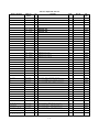
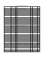
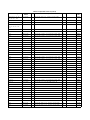
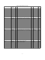
SPECIFICATIONS
Detailed specifications for the power supply are given in Table
1. All specifications are at front terminals with a resistive load,
and local sensing unless otherwise stated. Operating characteristics provide useful, but non-warranted information in the
form of the nominal performance.
Agilent Part No.
2110-0702
2110-0457
Table 1. Specifications and Operating Characteristics
*AC INPUT
*STABILITY (OUTPUT DRIFT)
An internal switch permits operation from 100, 115, or 230 Vac
lines.
100 Vac ± 10%, 47-63 Hz, 163 VA, 125 W
115 Vac ± 10%, 47-63 Hz, 163 VA, 125 W
230 Vac ± 10%, 47-63 Hz, 163 VA, 125 W
Maximum change in output for an 8 hours following a 30 minute
warm-up under constant line, load and ambient temperature.
Constant Voltage: Less than 0.1% plus 5 mV
Constant Current: Less than 0.1% plus 10 mA
LOAD TRANSIENT RESPONSE TIME
Less than 50 µsec for output recovery to within 15 mV following a
change in output current from full load to half load, or vice versa.
DC OUTPUT
Voltage and current can be programmed via front panel control or
remote analog control over the following ranges;
E3614A: 0 - 8 V, 0 - 6 A
E3615A: 0 - 20 V, 0 - 3 A
E3616A: 0 - 35 V, 0 - 1.7 A
E3617A: 0 - 60 V, 0 - 1 A
METER ACCURACY:B±(0.5% of output + 2 counts)Bat
25oC ± 5oC
METER (PROGRAMMING) RESOLUTION
Voltage: E3614A
E3615A
E3616A
E3617A
Current: E3614A
E3615A
E3616A
E3617A
*OUTPUT TERMINALS
The output terminals are provided on the front and rear panel.
They are isolated from the chassis and either the positive or negative terminal may be connected to the ground terminal.
LOAD REGULATION
Constant Voltage - Less than 0.01% plus 2 mV for a full load to no
load change in output current.
Constant Current - Less than 0.01% plus 250 µA for a zero to
maximum change in output voltage.
10 mV
10 mV (0 to 20 V), 100 mV (above 20 V)
10 mV (0 to 20 V), 100 mV (above 20 V)
10 mV (0 to 20 V), 100 mV (above 20 V)
10 mA
10 mA
1 mA
1 mA
*OVERLOAD PROTECTION
A continuously acting constant current circuit protects the power
supply for all overloads including a direct short placed across the
terminals in constant voltage operation. The constant voltage circuit limits the output voltage in the constant current mode of operation.
LINE REGULATION
Constant Voltage - Less than 0.01% plus 2 mV for any line voltage change within the input rating.
Constant Current - Less than 0.01% plus 250 µA for any line voltage change within the input rating.
*OVERVOLTAGE PROTECTION
Trip voltage adjustable via front panel control.
E3615A
E3616A
E3617A
E3614A
Range: 2.5-10 V 2.5-23 V
2.5-39 V
5-65 V
Margin: Minimum setting above output voltage to avoid
false tripping: 4% of output + 2 V for all models
PARD (Ripple and Noise)
Constant Voltage: Less than 200 µV rms and 1 mV p-p
(20 Hz-20 MHz).
Constant Current: E3614A: Less than 5 mA rms
E3615A: Less than 2 mA rms
E3616A: Less than 500 µA rms
E3617A: Less than 500 µA rms
*REMOTE ANALOG VOLTAGE PROGRAMMING (25 ± 5oC)
Remotely varied voltage from 0 to 10 V provides zero to maximum rated output voltage or current.
Voltage: Linearity 0.5% Current: Linearity 0.5%
The programming inputs are protected against input voltages up
to ±40 V.
OPERATING TEMPERATURE RANGE
0 to 40oC for full rated output. Maximum current is derated 1%
per degree C at 40oC-55oC.
*TEMPERATURE COEFFICIENT
REMOTE SENSING
Maximum change in output per oC after a 30-minute warm-up.
Constant Voltage: Less than 0.02% plus 500 µV.
Constant Current: E3614A: Less than 0.02% plus 3 mA
E3615A: Less than 0.02% plus 1.5 mA
E3616A: Less than 0.02% plus 1 mA
E3617A: Less than 0.02% plus 0.5 mA
Meets load-regulation specification when correcting for load-lead
drops of up to 0.5 V per lead with sense wire resistance of less
than 0.5 ohms per sense lead and lead lengths of less than 5
meters.
1-5
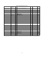
Table 1. Specifications and Operating Characteristics (Cont’d)
*REMOTE PROGRAMMING SPEED
DC ISOLATION
Maximum time required for output voltage to change from initial
value to within a tolerance band (0.1%) of the newly programmed
value following the onset of a step change in the programming
input voltage.
Full load
No load
Up:
E3614A:
3 msec
2 msec
E3615A:
9 msec
6 msec
85 msec
85 msec
E3616A:
200 msec
200 msec
E3617A:
Down: E3614A:
7 msec
1.6 sec
13 msec
2.2 sec
E3615A:
65 msec
1.8 sec
E3616A:
E3617A:
200 msec
3.2 sec
± 240 Vdc maximum between either output terminal and earth
ground including the output voltage.
INSTALLATION
instructions.
*COOLING: Convection cooling is employed.
*WEIGHT: 12.1 lbs/5.5 Kg net, 14.9 lbs/6.75 Kg shipping.
* Operating Characteristics
INITIAL INSPECTION
Before shipment, this instrument was inspected and found to be
free of mechanical and electrical defects. As soon as the instrument is unpacked, inspect for any damage that may have
occurred in transit. Save all packing materials until the inspection
is completed. If damage is found, a claim should be filed with the
carrier. The Agilent Technologies Sales and Service office should
be notified.
Mechanical Check
This check should confirm that there are no broken knobs or connectors, that the cabinet and panel surfaces are free of dents and
scratches, and that the meter is not scratched or cracked.
Electrical Check
The instrument should be checked against its electrical specifications. Paragraph "TURN-ON CHECKOUT PROCEDURE" contains a brief checkout procedure and "PERFORMANCE TEST" in
section SERVICE INFORMATION includes an instrument performance check to verify proper instrument operation.
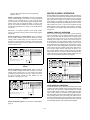
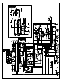
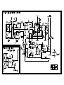
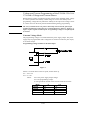
Figure 1. Outline Diagram
INPUT POWER REQUIREMENTS
The instrument is shipped ready for bench operation. It is necessary only to connect the instrument to a source of power and it is
ready for operation.
This power supply may be operated from nominal 100, 115, or
230 Vac 47-63 Hertz power source. A label on the rear panel
shows the nominal input voltage set for the unit at the factory. If
necessary, you can convert the supply to another nominal input
voltage by following the instructions below
Location and Cooling
Line Voltage Option Conversion
This instrument is air cooled. Sufficient space should be allowed so
that a free flow of cooling air can reach the sides and rear of the
instrument when it is in operation. It should be used in an area where
the ambient temperature does not exceed 40oC. Maximum current is
derated 1% per oC at 40oC-55oC.
Line voltage conversion is accomplished by adjusting two components: the line select switch and the rear panel fuse F1. To convert the supply from one line voltage option to another, proceed
as follows:
INSTALLATION DATA
a. Disconnect power cord.
b. Turn off the supply and remove the top cover by lifting the
cover upwards after taking it off from both sides of the chassis
by inserting a flat-blade screwdriver into the gap on the lower
rear portion of the cover.
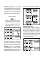
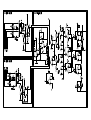
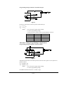
c. Set two sections of the line voltage selector switch on the PC
board for the desired line voltage (see Figure 2).
d. Check the rating of the fuse F1 installed in the rear panel fuse
holder and replace with the correct fuse if necessary. For 100
and 115 V operation, use a normal blow 2 A fuse and for 230
V use a time delay 1 A fuse.
Outline Diagram
Figure 1 is a outline diagram showing the dimensions of the
instrument.
Rack Mounting
This instrument may be rack mounted in a standard 19-inch rack
panel either by itself or alongside a similar unit. Please see
ACCESSORY, page 1-4, for available rack mounting accessories. Each rack-mounting kit includes complete installation
1-6
e. Replace the cover and mark the supply clearly with a tag or
label indicating the correct line voltage and fuse that is in
use.
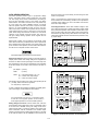
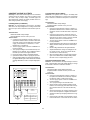
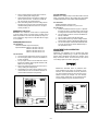
4. DISPLAY OVP/CC SET Switch: Pressing this switch causes
the VOLTS display to show voltage setting for overvoltage
shutdown (trip voltage) and the AMPS display to show the
current control set value. Setting values are either front panel
settings or remote voltage programmed settings.
5. OVP Adjust Screwdriver Control: While pressing the DISPLAY OVP/CC SET switch, rotating the control clock-wise
with a small, flat-blade screwdriver increases the setting for
overvoltage shutdown.
6. VOLTS Display: Digital display of actual output voltage, or
OVP shutdown setting.
7. AMPS Display: Digital display of actual output current, or
output-current setting.
8. CV LED Indicator: Output voltage is regulated when lighted.
This means the power supply is operating in the constant voltage mode.
9. CC LED Indicator: Output current is regulated when lighted.
This means the power supply is operating in the constant current mode.
10. OVP LED Indicator: Output is shutdown by the occurrence
of an overvoltage when lighted. Removing the cause of overvoltage and turning the power off, then on, resets the power
supply.
Figure 2. Line Voltage Selector (set for 115 Vac)
Power Cord
To protect operating personnel, the instrument should be
grounded. This instrument is equipped with a three conductor
power cord. The third conductor is the ground conductor and
when the power cord is plugged into an appropriate receptacle,
the supply is grounded.
The power supply was shipped with a power cord for the type of
outlet used at your location. If the appropriate cord was not
included, contact your nearest Agilent Sales Office to obtain the
correct cord.
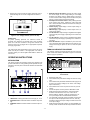
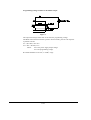
TURN-ON CHECKOUT PROCEDURE
The following checkout procedure describes the use of the front
panel controls and indicators illustrated in Figure 3 and ensures
that the supply is operational:
OPERATING INSTRUCTIONS
LOCAL
MASTER
_
+
+
_
+
_
INTRODUCTION
This section explains the operating controls and indicators and
provides information on many operating modes possible with your
instrument. The front panel controls and indicators are illustrated
in Figure 3.
M/S 1
M/S 2
SLAVE
CV
CC
SENSE
+S
OUT
-S
CV
CC
VREF A1 A2 A3
A4 A5
REMOTE
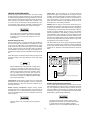
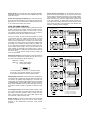
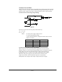
Figure 4. Switch Settings of Rear-Panel Control for TurnOn Checkout
a. Disconnect power cord.
b. Check that the rear-panel switch settings are as shown in Figure 4.
c. Check that the rear panel label indicates that the supply is set
to match your input line voltage (If not, refer to "Line Voltage
Option Conversion".).
d. Check that the fuse on the rear panel is correct for your line
voltage.
e. Connect the power cord and push the LINE switch to ON.
f. While pressing OVP/CC SET switch, verify that the OVP
shutdown is set above 8.0, 20.0, 35.0, or 60.0 Vdc for
E3614A, E3615A, E3616A, or E3617A respectively. If not,
turn up OVP Adjust with a small flat-blade screwdriver.
g. Turn VOLTAGE control fully counter clockwise to ensure that
the output of VOLTS display decreases to 0 Vdc, then fully
clockwise to ensure that output voltage increases to the maximum output voltage.
h. While pressing OVP/CC SET switch, turn the CURRENT control fully counter clockwise and then fully clockwise to ensure
Figure 3. Front-Panel Controls and Indicators
1. LINE Switch: Pressing this switch turns the supply on, or off.
2. VOLTAGE Control: Clockwise rotation increases output voltage.
3. CURRENT Control: Clockwise rotation increases output current.
1-7
that the current limit value can be set from zero to maximum
rated value.
False OVP shutdowns may occur if you set the OVP shutdown
too close to the supply's operating voltage. Set the OVP shutdown voltage 4% of output +2.0 V or more above the output voltage to avoid false shutdowns from load-induced transients.
OPERATING MODES
The setting of the rear panel switch determines the operating
modes of the power supply. The local operating mode is set so
the power supply senses the output voltage directly at the output
terminals (local sensing) for operation using the front panel controls (local programming). Other operating modes are: remote
voltage sensing and remote programming of output voltage and
current using external voltages.
Adjusting OVP. Follow this procedure to adjust the OVP shutdown voltage.
a. With the VOLTAGE control fully counter clockwise, turn on
the power supply.
b. While depressing DISPLAY OVP/CC SET switch, adjust
the OVP Adjust control to the desired OVP shutdown using
a small, flat-blade screwdriver.
c. Follow the procedure for CC or CV operaton to set the output voltage and current
LOCAL OPERATING MODE
The power supply is shipped from the factory configured in the
local operating mode. Local operating mode requires the switch
settings of the rear panel, as shown in Figure 4. The power supply provides constant voltage(CV) or constant current(CC) output.
Resetting OVP. If OVP shutdown occurs, reset the supply by
turning power off. Wait one or more seconds, and turn power on
again. If OVP shutdown continue to occur, check the connections
to the load and sense terminals, and check the OVP limit setting..
Constant Voltage Operaton
To set up a power supply for constant voltage operation, proceed
as follows:
a. Turn on the power supply and adjust 10-turn VOLTAGE control for desired output voltage (output terminals open).
b. While depressing DISPLAY OVP/CC SET switch, adjust 10turn CURRENT control for the desired current limit.
c. With power off connect the load to the output terminals.
d. Turn on the power supply. Verify that CV LED is lighted.
During actual operation, if a load change causes the current
limit to be exceeded, the power supply will automatically
cross over to constant current mode and the output voltage
will drop proportionately.
Strong electrostatic discharge to power supply can make
OVP trip and eventually crowbar the output, which can
effectively protect output loads from the hazardous ESD
current.
CONNECTING LOADS
The output of the supply is isolated from earth ground. Either output terminal may be grounded or the output can be floated up to
240 volts off ground. Total output voltage to ground must not
exceed 240 Vdc.
Constant Current Operation
To set up a power supply for constant current operation, proceed
as follows:
Each load should be connected to the power supply output terminals
using separate pairs of connecting wires. This will minimize mutual
coupling effects between loads and will retain full advantage of the
low output impedance of the power supply. Each pair of connecting
wires should be as short as possible and twisted or shielded to
reduce noise pick-up. (If a shield is used, connect one end to the
power supply ground terminal and leave the other end unconnected.)
a. Turn on power supply.
b. While depressing DISPLAY OVP/CC SET switch, adjust
CURRENT control for the desired output current.
c. Turn up the VOLTAGE control to the desired voltage limit.
d. With power off connect the load to the output terminal.
e. Turn on power supply and then verify that CC LED is lighted.
(If CV LED is lighted, choose a higher voltage limit. A voltage
setting that is greater than the current setting multiplied by the
load resistance in ohms is required for CC operation.) During
actual operation, if a load change causes the voltage limit to
be exceeded, the power supply will automatically cross over
to constant voltage operation at the preset voltage limit and
output current will drop proportionately.
If load considerations require that the output power distribution
terminals be remotely located from the power supply, then the
power supply output terminals should be connected to the remote
distribution terminals via a pair of twisted or shielded wires and
each load separately connected to the remote distribution terminals. For this case, remote sensing should be used (See paragraph "Remote Voltage Sensing").
Overvoltage Protection (OVP)
Adjustable overvoltage protection guards your load against overvoltage. When the voltage at the output terminals increases (or is
increased by an external source) to the OVP shutdown voltage as
set by the OVP ADJUST control, the supply's OVP circuit disables the output causing the output voltage and current to drop to
zero. During OVP shutdown the OVP LED lights.
OPERATION BEYOND RATED OUTPUT
The output controls can adjust the voltage or current to values up
to 5% over the rated output. Although the supply can be operated
in the 5% overrange region without being damaged, it can not be
guaranteed to meet all of its performance specifications in this
region.
1-8
REMOTE OPERATING MODES
Output Noise. Any noise picked up on the sense leads will
appear at the supply's output voltage and may degrade CV load
regulation. Twist the sense leads to minimize the pickup of external noise and run them parallel and close to the load leads. In
noisy environments, it may be necessary to shield the sense
leads. Ground the shield at the power supply end only. Do not use
the shield as one of the sensing conductors.
Remote operating modes discussed below are remote voltage
sensing and remote voltage programming. You can set up the unit
for remote operating modes by changing the settings of the rear
panel switch and connecting the leads from the rear panel terminals to the load or the external voltage. Solid conductors of 0.75
to 1.5 mm2 can be connected to the rear panel terminals by simply push fitting. Thinner wires or conductors are inserted into the
connection space after depressing the orange opening lever.
Stability. When the supply is connected for remote sensing, it is
possible for the impedance of the load wires and the capacitance
of the load to form a filter, which will become part of the supply's
CV feedback loop. The extra phase shift created by this filter can
degrade the supply's stability and can result in poor transient
response performance or loop stability. In extreme cases, it can
cause oscillations. Keep the leads as short as possible and twist
the leads of the load to eliminate the load lead inductance and
keep the load capacitance as small as possible.The load leads
should be of the largest diameter practical, heavy enough to limit
the voltage drop in each lead to 0.5 volts.
Turn off the supply while making changes to rear panel
switch settings or connections. This avoids the possibility
of damage to the load and OVP shutdown from unintended output.
Remote Voltage Sensing
Remote voltage sensing is used to maintain good regulation at
the load and reduce the degradation of regulation that would
occur due to the voltage drop in the leads between the power
supply and the load. By connecting the supply for remote voltage
sensing, voltage is sensed at the load rather than at the supply's
output terminals. This will allow the supply to automatically compensate for the voltage drop in the load leads and improve regulation.
The sense leads are part of the supply's programming feedback
control loop. Accidental open-connections of sense or load leads
during remote sensing operation have various unwanted effects.
Provide secure, permanent connections-especially for the sense
leads.
LOCAL
MASTER
When the supply is connected for remote sensing, the OVP circuit
senses the voltage at the sense leads and not the main output
terminals.
M/S 1
M/S 2
CV
CC
SLAVE
Remote voltage sensing compensates for a voltage drop of
up to 0.5 V in each load, and there may be up to a 0.1 V
drop between the output terminal and the internal sensing
resistor, at which point the OVP circuit is connected. Therefore, the voltage sensed by the OVP circuit could be as
much as 1.1 V more than the voltage being regulated at the
load. It may be necessary to re-adjust the OVP trip voltage
when using remote sensing.
_
+
SENSE
+S
OUT
+
-S
_
CV
+
CC
_
VREF A1 A2 A3 A4 A5
REMOTE
+
nqcf
_
pqvg\BvBBBBB
CV Regulation. Notice that any voltage drop in the sense leads
adds directly to the CV load regulation. In order to maintain the
specified performance, keep the sense lead resistance to 0.5
ohms per lead or less.
Figure 5. Remote Voltage Sensing
Remote Analog Voltage Programming
Remote analog voltage programming permits control of the regulated output voltage or current by means of a remotely varied voltage. The programming (external) voltage should not exceed 10
volts. The stability of the programming voltages directly affects
the stability of the output. The voltage control on the front panel is
disabled during remote analog programming.
Remote Sensing Connections. Remote sensing requires
changing settings of the rear panel switch and connecting the
load leads from + and - output terminals to the load and connecting the sense leads from the +S and -S terminals to the load as
shown in Figure 5.
The supply includes clamp circuits to prevent it from
supplying more than about 120% of rated output voltage
or current when the remote programming voltage is
greater than 10 Vdc. Do not intentionally operate the sup-
Observe polarity when connecting the sensing leads to
the load.
1-9
MULTIPLE-SUPPLY OPERATION
ply above 100% rated output. Limit your programming
voltage to 10 Vdc.
Normal parallel and auto-parallel operation provides increased output current while normal series and auto-series provides increased
output voltage. Auto-tracking provides single control of output voltage of more than one supply. You can set up the unit for multiplesupply operation by changing the settings of the rear panel switch
and connecting the leads from the rear panel terminals to the load.
Remote Programming Connections. Remote programming
requires changing settings of the switch and connecting external
voltages to + and - terminals of "CV" or "CC" on the rear panel.
Any noise picked up on the programming leads will appear on the
supply's output and may degrade regulation. To reduce noise
pick-up, use a twisted or shielded pair of wires for programming,
with the shield grounded at one end only. Do not use the shield as
a conductor.
Solid conductors of 0.75 to 1.5 mm2 can be connected to the rear
panel terminals by simply push fitting. Thinner wires or conductors
are inserted into the connection space after depressing the orange
opening lever.
Notice that it is possible to operate a power supply simultaneously in the remote sensing and the remote analog programming modes.
NORMAL PARALLEL OPERATION
Two or more power supplies being capable of CV/CC automatic
cross over operation can be connected in parallel to obtain a total
output current greater than that available from one power supply.
The total output current is the sum of the output currents of the
individual power supplies. The output of each power supply can
be set separately. The output voltage controls of one power supply should be set to the desired output voltage; the other power
supply should be set for a slightly higher output voltage. The supply with the higher output voltage setting will deliver its constant
current output, and drop its output voltage until it equals the output of the other supply, and the other supply will remain in constant voltage operation and only deliver that fraction of its rated
output current which is necessary to fulfill the total load demand.
Figure 8 shows the rear panel switch settings and terminal connections for normal parallel operation of two supplies.
Remote Programming, Constant Voltage. Figure 6 shows the
rear panel switch settings and terminal connections for remotevoltage control of output voltage. A 1 Vdc change in the remote
programming voltage produces a change in output voltage (voltage gain) as follows: E3614A: 0.8 Vdc, E3615A: 2 Vdc, E3616A:
3.5 Vdc, E3617A: 6 Vdc
LOCAL
MASTER
M/S 1
M/S 2
CV
CC
SLAVE
_
+
SENSE
OUT
+S
+
-S
_
_
+
CV
CC
VREF A1
A2
A3
A4
A5
REMOTE
NOTE:
POWER SUPPLY
LOCAL
MASTER
See the supplementary Manual, if you are not using
_
+
+
_
+
_
isolated programming voltage source.
Figure 6. Remote Voltage Programming, Constant
Voltage
M/S 1 M/S 2
SLAVE
Remote Programming, Constant Current. Figure 7 shows the
rear panel switch settings and terminal connections for remotevoltage control of output current. A 1 Vdc change in the remote
programming voltage produces a change in output current (current gain) as follows: E3614A: 0.6 Adc, E3615A: 0.3 Adc,
E3616A: 0.17 Adc, E3617A: 0.1 Adc
_
+
+
_
CC
SENSE
OUT
+S
-S
CC VREF A1 A2 A3 A4 A5
CV
REMOTE
LOAD
POWER SUPPLY
LOCAL
MASTER
M/S 1 M/S 2
SLAVE
LOCAL
MASTER
CV
CV
CC
+
SENSE
+S
_
OUT
+
-S
CV
_
+
_
CC VREF A1 A2 A3 A4 A5
REMOTE
_
+
Figure 8. Normal Parallel Operation of Two Supplies
AUTO-PARALLEL OPERATION
M/S 1
M/S 2
SLAVE
CV
CC
SENSE
+S
OUT
-S
CV
CC
VREF A1
A2
A3
A4
Auto-parallel operation permits equal current sharing under all load
conditions, and allows complete control of output current from one
master supply. The control unit is called the master; the controlled
units are called slaves. Normally, only supplies having the same
model number should be connected for auto-parallel operation,
since the supplies must have the same voltage drop across the current monitoring resistor at full current rating. The output current of
each slave is approximately equal to the master's. Figure 9 and Figure 10 show the rear panel switch settings and terminal connections
for auto-parallel operation of two supplies and three supplies.
A5
REMOTE
NOTE:
See the supplementary Manual, if you are not using
isolated programming voltage source.
Figure 7. Remote Voltage Programming, Constant
Current
Remote Programming Speed. See the table of Specifications,
page 1-5.
1-10
Setting Voltage and Current. Turn the slave unit's CURRENT
control fully clockwise. Adjust the master unit's controls to set the
desired output voltage and current. The master supply operates
in a completely normal fashion and may be set up for either constant voltage or constant current operation as required. Verify that
the slave is in CV operation.
gramming according to the remote-programming instructions.
MASTER POWER SUPPLY
For auto-parallel operation of two supplies, the combined output
voltage is the same as the master unit's voltage setting, and the
combined output current is two times the master unit's current. In
general, for two supplies, the auto-parallel output current(Io) is
M/S 1
M/S 2
CV
SLAVE
CC
_
+
LOCAL
MASTER
SENSE
OUT
+S
+
-S
_ + _
CC VREF A1 A2 A3 A4 A5
CV
REMOTE
LOAD
SLAVE POWER SUPPLY
M/S 1
M/S 2
CV
SLAVE
CC
SENSE
OUT
+S
+ _ + _
_
+
LOCAL
MASTER
Io = Im + Is = 2Im
where Im = master unit's output current
Is = slave unit's output current
-S
CV
CC VREF A1 A2 A3 A4 A5
REMOTE
SLAVE POWER SUPPLY
Proportional currents from auto-paralleled units require
equal load-lead voltage drops. Connect each supply to
the load using separate pairs of wire with length chosen
to provide equal voltage drops from pair to pair. If this is
not feasible, connect each supply to a pair of distribution
terminals using equal- voltage-drop wire pairs, and then
connect the distribution terminals to the load with a single
pair of leads.
M/S 1
LOCAL
M/S 1 M/S 2
SLAVE
CV
CC
_
+
SENSE
OUT
+S
+
-S
_
+
_
LOAD
SLAVE POWER SUPPLY
LOCAL
M/S 1 M/S 2
SLAVE
CV
CC
+
SENSE
+S
_
OUT
+
-S
CV
_
+
SENSE
OUT
+S
-S
CC VREF A1 A2 A3 A4 A5
CV
REMOTE
Series operation of two or more power supplies can be accomplished up to the output isolation rating of any one supply to
obtain a higher voltage than that available from a single supply.
Series connected supplies can be operated with one load across
both supplies or with a separate load for each supply. These
power supplies have a reverse polarity diode connected across
the output terminals so that if operated in series with other supplies, damage will not occur if the load is short-circuited or if one
supply is turned on separately from its series partners. When this
connection is used, the output voltage is the sum of the voltages
of the individual supplies. Each of the individual supplies must be
adjusted in order to obtain the total output voltage. Figure 11
shows the rear panel switch settings and terminal connections for
normal series operation of two supplies.
REMOTE
MASTER
CC
NORMAL SERIES OPERATION
CC VREF A1 A2 A3 A4 A5
CV
CV
Figure 10. Auto-Parallel Operation of Three Supplies
MASTER POWER SUPPLY
MASTER
M/S 2
SLAVE
+ _ + _
_
+
LOCAL
MASTER
_
CC VREF A1 A2 A3 A4 A5
REMOTE
POWER SUPPLY
Figure 9. Auto-Parallel Operation of Two Supplies
LOCAL
MASTER
Overvoltage Protection. Adjust the desired OVP shutdown limit
using the master unit's OVP Adjust control. Set the slave units'
OVP limits above the master's. When a master-unit shuts down,
the master programs the slave units to zero voltage output. If a
slave unit shuts down, it shuts only itself down. If the required current is great enough, the master will switch from CV to CC operation.
M/S 1 M/S 2
SLAVE
CV
CC
_
+
SENSE
OUT
+S
+
-S
_
CV
+
_
CC VREF A1 A2 A3 A4 A5
REMOTE
LOAD
POWER SUPPLY
LOCAL
MASTER
+
_
+
_
+
_
Remote Sensing. To remote sense with auto-parallel operation,
connect remote-sense leads only to the master unit according to
the remote-sensing instructions.
M/S 1 M/S 2
SLAVE
Remote Analog Voltage Programming. To remote program with
auto-parallel operation, set up only the master unit for remote pro-
CV
CC
SENSE
+S
OUT
-S
CV
CC VREF A1 A2 A3 A4 A5
REMOTE
Figure 11. Normal Series Operation of Two Supplies
1-11
AUTO-SERIES OPERATION
above the master unit's current setting to avoid having the slave
switch to CC operation.
Auto-series operation permits equal or proportional voltage
sharing, and allows control of output voltage from one master
unit. The voltage of the slaves is determined by the setting of
the front panel VOLTAGE control on the master and voltage
divider resistor. The master unit must be the most positive supply of the series. The output CURRENT controls of all series
units are operative and the current limit is equal to the lowest
setting. If any output CURRENT controls are set too low, automatic cross over to constant current operation will occur and the
output voltage will drop. Figure 12 and Figure 13 show the rear
panel switch settings and terminal connections for Auto-series
operation of two supplies and three supplies. This mode can
also give ±voltage tracking operation of two supplies with two
separate loads.
When in CC operation the combined output current is the same
as the master unit's current setting, and when in CV operation the
combined output voltage is the sum of the master unit's and the
slave unit's output voltages.
Overvoltage Protection. Set the OVP shutdown voltage in each
unit so that it shuts down at a voltage higher than its output voltage
during auto-series operation. When a master unit shuts down, it programs any slave units to zero output. When a slave unit shuts down,
it shuts down only itself (and any slaves below it in the stack). The
master (and all slaves above the shut-down slave) continues to supply output voltage.
Mixed model numbers may be employed in auto-series combination without restriction, provided that each slave is specified as
being capable of auto-series operation. If the master supply is set
up for constant current operation, then the master-slave combination will act as a composite constant current source.
MASTER POWER SUPPLY
LOCAL
MASTER
M/S 1 M/S 2
SLAVE
CV
CC
_
+
SENSE
OUT
+S
_
+
-S
CV
+
_
CC VREF A1 A2 A3 A4 A5
REMOTE
LOAD
R1
R2
SLAVE POWER SUPPLY
Total output voltage to ground must not exceed 240 Vdc.
LOCAL
MASTER
Determining Resistors. External resistors control the fraction (or
multiple) of the master unit's voltage setting that is supplied from
the slave unit. Notice that the percentage of the total output voltage contributed by each supply is independent of the magnitude
of the total voltage. For two units in auto-series the ratio of R1 to
R2 is
M/S 1 M/S 2
SLAVE
CV
CC
_
+
SENSE
OUT
+S
_
+
-S
CV
+
_
CC VREF A1 A2 A3 A4 A5
REMOTE
Figure 12. Auto-Series Operation of Two Supplies
(R1+R2)/R1 = (Vo/Vm)
R2/R1
= (Vs/Vm)
MASTER POWER SUPPLY
+
LOCAL
MASTER
Where
_
+
Vo = auto-series voltage = Vs + Vm
Vm = master unit's output voltage
Vs = slave unit's output voltage
M/S 1
For example, using the E3617A as a slave unit and putting R2=50
kΩ (1/4 watt), then from the above equations,
R1 = R2(Vm/Vs) = 50(Vm/Vs) kΩ
M/S 2
CV
SLAVE
CC
SENSE
+S
OUT
-S
CV
_ + _
CC VREF A1 A2 A3 A4 A5
REMOTE
LOAD
R1
R2
SLAVE POWER SUPPLY(S1)
+
LOCAL
MASTER
_
+
_ + _
In order to maintain the temperature coefficient and stability performance of the supply, choose stable, low noise resistors.
M/S 1
M/S 2
CV
SLAVE
CC
SENSE
+S
OUT
-S
CV
CC VREF A1 A2 A3 A4 A5
REMOTE
R3
It is recommended to connect a 0.1 µF capacitor in parallel with R2 in two supplies operation or R2 and R4 in
three supplies operation to ensure the stable operation.
R4
SLAVE POWER SUPPLY(S2)
Setting Voltage and Current. Use the master unit's controls to
set the desired output voltage and current. The VOLTAGE control
of the slave unit is disabled. Turning the voltage control of the
master unit will result in a continuous variation of the output of the
series combination, with the contribution of the master's output
voltage to that of the slave's voltage always remaining in the ratio
of the external resistors. Set the CURRENT control of slave unit
M/S 1
M/S 2
SLAVE
+
LOCAL
MASTER
CV
CC
SENSE
+S
OUT
_
+
-S
CV
_ + _
CC VREF A1 A2 A3 A4 A5
REMOTE
R2 R2 R4
)
Vo=Vm(1+ +
R1 R1 R3
Where
Vo = Auto-Series voltage = Vm + Vs1 + Vs2
Vm = master unit's output voltage
Vs1 = slave(S1) unit's output voltage
Vs2 = slave(S2) unit's output voltage
Figure 13. Auto-Series Operation of Three Supplies
1-12
Remote Sensing. To remote sense with auto-series operation,
set SENSE switch of the master unit and set SENSE switch of the
slave unit to remote.
Remote Analog Programming. To simultaneously remote program both units' output voltages, set up only the master unit for
remote voltage programming according to the remote programming instructions. To vary the fraction of the output voltage contribution by the slave unit, connect a variable resistor in place of R2
in two units operation. To independently remote program each
unit's output current setting, set up each unit for remote control of
output current according to the instructions under "Remote Programming, Constant Current" paragraph.
Remote Analog Voltage Programming. To remote analog program with auto-series operation, connect program (external) voltages to the "CV" or "CC"" terminal of the master unit and set "CV"
or "CC" switch of the master unit to remote.
AUTO-TRACKING OPERATON
Auto-tracking operation of power supplies is similar to auto-series
operation except that the master and slave supplies have the
same output polarity with respect to a common bus or ground.
This operation is useful where simultaneous turn-up, turn-down or
proportional control of all power supplies is required.
MASTER POWER SUPPLY
LOCAL
MASTER
M/S 1 M/S 2
SLAVE
Figure 14 and Figure 15 show two and three supplies connected
in auto-tracking with their negative output terminals connected
together as a common or ground point. For two units in autotracking a fraction R2/(R1+R2) of the output of the master supply
is provided as one of the inputs to the comparison amplifier of the
slave supply, thus controlling the slave's output. The master supply in an auto-tracking operation must be the positive supply having the largest output voltage. Turn-up and turn-down of the
power supplies are controlled by the master supply. In order to
maintain the temperature coefficient and stability specifications of
the power supply, the external resistor should be stable, low
noise, low temperature.
CV
CC
_
+
SENSE
+
OUT
+S
-S
_
CV
+
_
CC VREF A1 A2 A3 A4 A5
REMOTE
LOAD
R1
R2
LOAD
SLAVE POWER SUPPLY
LOCAL
MASTER
M/S 1 M/S 2
SLAVE
CV
CC
_
+
SENSE
+
OUT
+S
-S
CV
_
+
_
CC VREF A1 A2 A3 A4 A5
REMOTE
Figure 14. Auto-Tracking Operation of Two Supplies
Determining Resistors. External resistors control the fraction of
the master unit's voltage that is supplied from the slave unit. For
two units in auto-tracking the ratio R1 and R2 is
MASTER POWER SUPPLY
R2/(R1+R2 = (Vs/Vm)
Where Vm = master output voltage
Vs = slave output voltage
M/S 1
M/S 2
+
LOCAL
MASTER
CV
SLAVE
CC
SENSE
+S
_
OUT
+
-S
CV
_ + _
CC VREF A1 A2 A3 A4 A5
REMOTE
LOAD
Setting Voltage and Current. Use the master unit's VOLTAGE control to set the output voltage from both units. When the master is in
CV operation, the master's output voltage(Vm) is the same as its
voltage setting, and the slave's output voltage for two units operation
is Vm(R2/(R1+R2)). The VOLTAGE control of the slave unit is disabled. Set the CURRENT controls of master and slave units above
the required currents to assure CV operation of master and slave
units.
M/S 1
M/S 2
+
LOCAL
MASTER
It is recommended to connect a 0.1 µF capacitor in parallel with R2 in two supplies operation or R2 and R4 in
three supplies operation to ensure the stable operation.
CV
SLAVE
CC
R1
LOAD
SLAVE POWER SUPPLY(S1)
SENSE
+S
OUT
-S
CV
CC VREF A1 A2 A3 A4 A5
REMOTE
R3
M/S 1
M/S 2
+
LOCAL
MASTER
CV
SLAVE
R2
Vs1 =
Vm
R1+ R2
R4
Vs2 =
Vs1
R3+ R4
CC
R4
LOAD
SLAVE POWER SUPPLY(S2)
Overvoltage Protection. Set the OVP shutdown voltage in each
unit so that it shuts down at a voltage higher than its output voltage during auto-tracking operation. When a master unit shuts
down, it programs any slave units to zero output. When a slave
unit shuts down, it shuts down only itself.
R2
_ + _
+
_
SENSE
+S
OUT
_ + _
+
_
-S
CV
CC VREF A1 A2 A3 A4 A5
REMOTE
Where
Vm = masters unit's output voltage
Vs1 = slave(S1) unit's output voltage
Vs2 = slave(S2) unit's output voltage
Figure 15. Auto-Tracking Operation of Three Supplies
Remote Sensing. To include remote sensing with auto-tracking
operation independently, set up each unit for remote sensing
according to the remote-sensing instructions under previous
paragraph.
1-13
LOAD CONSIDERATIONS
a. The output impedance of the power supply decreases with
increasing frequency.
b. The recovery time of the output voltage is longer for load
resistance changes.
c. A large surge current causing a high power dissipation in the
load occurs when the load resistance is reduced rapidly.
This section provides information on operating your supply with
various types of loads connected to its output.
PULSE LOADING
The power supply will automatically cross over from constantvoltage to constant current operation in response to an increase
(over the preset limit) in the output current. Although the preset
limit may be set higher than the average output current, high peak
currents (as occur in pulse loading) may exceed the preset current limit and cause cross over to occur. If this cross over limiting
is not desired, set the preset limit for the peak requirement and
not the average.
REVERSE VOLTAGE LOADING
A diode is connected across the output terminals with reverse
polarity. This diode protects the output electrolytic capacitors and
the series regulator transistors from the effects of a reverse voltage applied across the output terminals. For example, in series
operation of two supplies, if the AC is removed from one supply,
the diode prevents damage to the unenergized supply which
would otherwise result from a reverse polarity voltage.
REVERSE CURRENT LOADING
An active load connected to the power supply may actually
deliver a reverse current to the power supply during a portion of
its operating cycle. An external source can not be allowed to
pump current into the supply without loss of regulation and possible damage to the output capacitor of the power supply. To avoid
these effects, it is necessary to preload the supply with a dummy
load resistor so that the power supply delivers current through the
entire operating cycle of the load devices.
Since series regulator transistors cannot withstand reverse voltage, another diode is connected across the series transistor. This
diode protects the series regulators in parallel or auto-parallel
operation if one supply of the parallel combination is turned on
before the other.
BATTERY CHARGING
The power supply's OVP circuit contains a crowbar SCR, which
effectively shorts the output of the supply whenever the OVP trips. If
an external voltage source such as a battery is connected across the
output, and OVP inadvertently triggered, the SCR will continuously
sink a large current from the source; possibly damaging the supply.
To avoid this a diode must be connected in series with the output as
shown in Figure 17.
Figure 16. Reverse Current Loading Solution
Figure 17. Recommended Protection Circuit for
Battery Charging
OUTPUT CAPACITANCE
An internal capacitor, connected across the output terminals of
the power supply, helps to supply high-current pulses of short
duration during constant voltage operation. Any capacitance
added externally will improve the pulse current capability, but will
decrease the safety provided by the current limiting circuit. A
high-current pulse may damage load components before the
average output current is large enough to cause the current limiting circuit to operate.
The effect of the output capacitor during constant current operation are as follows:
1-14
SERVICE INFORMATION
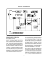
Figure A-1. Block Diagram
PRINCIPLES OF OPERATION
The main secondary winding of the power transformer has
three sections (N1, N2, and N3), each of which has a different
turns ratio with respect to the primary winding. At the beginning of each half-cycle of the input ac, the control circuit
determines whether one pair, both or none of the SCR will be
fired. If neither SCR is fired, the bridge diode (CR13) receives
an ac input voltage that is determined by N1 turns and the
input capacitors charge to a corresponding level. If SCR
CR15 and CR18 are fired, input capacitors charge to the voltage determined by N1+N2 turns. Similarly, if CR10 and CR12
are fired the capacitors are charged by N1 + N3. Finally, if all
SCRs are fired simultaneously, input capacitors charge to its
highest voltage level determined by N1 + N2 + N3 turns.
(Block Diagram Overview)
Throughout this discussion, refer to both the block diagram of
Figure A-1 and the schematic diagrams at the rear of the
manual. The input ac line voltage is first applied to the preregulator which operates in conjunction with the SCR control circuit (preregulator control circuit) to rectify the tap switched AC
voltage. This preregulator minimizes the power dissipated in
the series regulating elements by controlling the dc level
across the input filter capacitor, depending on the output voltage.
To achieve this, tap switching is accomplished by four SCRs
and one bridge diode (CR10, CR12, CR15, CR18 and CR13)
and the SCR control circuit. By selecting different SCR firing
combinations from SCR control circuit, these circuits allow the
input capacitors (C7 and C8) to charge to one of four discrete
voltage levels, depending on the output voltage required.
The SCR control circuit determines which SCRs are to be
fired by monitoring the output voltage and comparing these
values against a set of three internally derived reference levels. These three reference levels are translated into boundary
lines to allow the output characteristic to be mapped into four
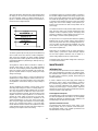
operating regions (Figure A-2). The boundary lines, which are
invisible to the user, are divided into four operating regions
(V1, V2, V3, and V4) to minimize the power dissipation in the
A-1
series pass transistors. Whenever the output voltage is below
the sloping V1 line, the control circuit inhibits four SCRs and
the input capacitors charge to a voltage determined by N1.
Figure A-2 indicates the windings that are connected as a
result of the other voltage decisions.
Full protection against any overload condition is inherent in
the Constant Voltage/Constant Current design principle since
there is not any load condition that can cause an output which
lies outside the operating region. For either constant voltage
or constant current operation, the proper choice of front panel
voltage and current control settings insures optimum protection for the load device as well as full protection for the
power supply.
The reference and bias circuit provides stable reference voltages which are used by the constant voltage/current error
amplifier circuits for comparison purpose. The display circuit
provides an indication of output voltage and current for constant voltage or constant current operating modes.
An operator error or a component failure within the regulating
feedback loop can drive a power supply's output voltage to
many times its preset value. The overvoltage protection circuit is to protect the load against this possibility. The circuit
insures that the power supply voltage across the load will
never exceed a preset limit.
Figure A-2. Output Power Plot
Diode CR19 is connected across the output terminals in
reverse polarity. It protects the output electrolytic capacitor
and the series regulator transistors from the effects of a
reverse voltage applied across the output terminals.
The series regulators (Q1 and Q4) are part of a feedback loop
which consists of the driver and the Constant Voltage/Constant Current error amplifier. The series regulator feedback
loop provides "fine and fast" regulation of the output while the
preregulator feedback loop handles large, relatively slow, regulation demands.
The display power circuit provides voltage which is used by A/
D converter and LED drive.
MAINTENANCE
The regulator is made to alter its conduction to maintain a
constant output voltage or current. The voltage developed
across the current sampling resistors (R58 and R59) is the
input to the constant current error amplifier. The constant voltage error amplifier obtains its input by sampling the output
voltage of the supply.
INTRODUCTION
This section provides performance test and calibration procedures and troubleshooting information. The following operation verification tests comprise a short procedure to verify that
the power supply is performing properly, without testing all
specified parameters.
Any changes in output voltage or current are detected and
amplified by the constant voltage or constant current error circuit and applied to the series regulator in the correct phase
and amplitude to counteract the change in output voltage or
current.
If a fault is detected in the power supply while making the
performance check or during normal operation, proceed to
the troubleshooting procedures. After troubleshooting, perform any necessary adjustments and calibrations. Before
returning the power supply to normal operation, repeat the
performance check to ensure that the fault has been properly
corrected and that no other faults exist.
Two error amplifiers are included in a CV/CC supply, one for
controlling output voltage, the other for controlling output current. Since the constant voltage amplifier tends to achieve
zero output impedance and alters the output current whenever the load resistance changes, while the constant current
amplifier causes the output impedance to be infinite and
changes the output voltage in response to any load resistance change, it is obvious that the two amplifiers can not
operate simultaneously. For any given value of load resistance, the power supply must act either as a constant voltage
source or as a constant current source - it can not be both;
transfer between these two modes is accomplished at a value
of load resistance equal to the ratio of the output voltage control setting to the output current control setting.
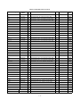
Test Equipment Required
The following Table A-1 lists the equipment required to perform
the tests and adjustments of this section. You can separately
identify the equipment for performance tests, calibration, and
troubleshooting in the USE column of the table.
Operation Verification Tests
The following tests assure that the power supply is performing properly. They do not, however, check all the specified parameters tested in the complete performance test
described below. Proceed as follows:
A-2
Electronic Load. The test and calibration procedures use an
electronic load to test the supply quickly and accurately. An
electronic load is considerably easier to use than load resistor. It eliminates the need for connecting resistors or rheostats
in parallel to handle the power, it is much more stable than
carbon-pile load, and it makes easy work of switching
between load conditions as is required for the load regulation
and load transient response tests.
a. Perform turn-on checkout procedure given in page 1-7.
b. Perform the CV and CC Load Regulation performance tests given in the following paragraphs
respectively.
PERFORMANCE TESTS
The following paragraphs provide test procedures for verifying the power supply's compliance with the specifications of
Table 1. Please refer to adjustment and calibration or troubleshooting procedure if you observe any out of specification
performance.
Current Monitoring Resistor Rs. To eliminate output-current
measurement error caused by voltage drops in the leads and
connections, connect the current monitoring (sampling) resistor between -OUT and the load as a four-terminal device. Figure A-3 shows correct connections. Connect the current
monitoring test leads inside the load lead connections directly
at the monitoring resistor element. Select a resistor with stable characteristics and lower temperature coefficient (see
Table A-1).
Measurement Techniques
Setup for All Tests. Measure the output voltage directly at the
+S and -S terminals on the rear panel; in this way the monitoring
device sees the same performance as the feedback amplifier
within the power supply. Failure to connect the monitoring device
to the proper points shown in Figure A-3 will result in the measurement not of the power supply characteristics, but of the
power supply plus the resistance of the leads between its output
terminals and the point of connection.
Use separate leads to all measuring devices to avoid the subtle mutual coupling effects that may occur between measuring devices unless all are returned to the low impedance
terminals of the power supply. Twisted pairs or shielded cable
should be used to avoid pickup on the measuring leads.
Figure A-3. Current Monitoring Resistor Connections
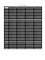
Table A-1. Test Equipment Required
TYPE
REQUIRED CHARACTERISTICS
USE
RECOMMENDED MODEL
Oscilloscope
Sensitivity : 1 mV
Bandwidth : 20 MHz/100 MHz
Input : Differential, 50 ohm and 100 ohm
P, T
Agilent 54600A
RMS Voltmeter
True rms, 20 MHz bandwidth
Sensitivity : 1 mV
Accuracy : 5%
P
Multimeter
Resolution : 100 nV
Accuracy : 0.0035%
P, A, T
Agilent 34401A
Electronic Load
Voltage Range : 240 Vdc
Current Range : 10 Adc
Open and short switches
Transient on/off
P
Agilent 6063A
Load Resistor (RL)
1.3 ohm 60 W, 6.6 ohm 60 W, 20.5 ohm 60 W,
60 ohm 60 W
P
Current Monitoring
(Sampling) Resistor (RS)
0.1 ohm 0.1% 10 W, 1 ohm 1% 5 W
P, A
Variable Voltage
Auto Transformer
Range : 85-130 and 200-260 Volts
P, T
* P = Performance testing A = Calibration adjustments T = Troubleshooting.
A-3
CONSTANT VOLTAGE (CV) TESTS
Line Regulation (Source Effect)
CV Setup. For all CV tests set the output current at full rated
output to assure CV operation. The onset of constant current
can cause a drop in output voltage, increased ripple, and
other performance changes not properly ascribed to the constant voltage operation of the supply.
Definition: Line regulation is the change in the steady state
value of dc output voltage due to a change in ac input voltage
from a minimum to a maximum value(±10% of nominal voltage).
Test Parameter:
Measured Variable: Output Voltage
Expected Results: Less than 0.01% plus 2 mV
Test Procedure:
a. Connect the test equipment as shown in Figure A-4.
Operate the electronic load in constant current mode
and set its current to the full rated value of the power
supply.
b. Connect the supply to the ac power line through a
variable autotransformer which is set for low line voltage(104 Vac for nominal 115 Vac, 90 Vac for nominal
100 Vac, and 207 Vac for nominal 230 Vac).
c. Turn the supply's power on and turn CURRENT control fully clockwise.
d. Adjust VOLTAGE control until the front panel VOLTS
display indicates exactly the maximum rated output
voltage.
e. Record voltage indicated on the digital voltmeter.
f. Adjust autotransformer to high line voltage(127 Vac
for nominal 115 Vac, 110 Vac for nominal 100 Vac,
and 253 Vac for nominal 230 Vac).
g. When the reading settles, record the output voltage
again. Check that the two recorded readings differ
less than 0.01% of output voltage plus 2 mV.
Load Regulation (Load Effect)
Definition: CV Load regulation is the change in the steady
state value of dc output voltage due to a change in load resistance from open circuit to full load or from full load to open circuit.
Test Parameters:
Measured Variable: Output Voltage
Expected Results: Less than 0.01% plus 2 mV
Test Procedure:
a. Connect the test equipment as shown in Figure A-4.
Operate the electronic load in constant current mode
and set its current to the full rated value of the power
supply (6 A for E3614A, 3 A for E3615A, 1.7 A for
E3616A and 1 A for E3617A).
b. Turn the supply's power on and turn CURRENT control fully clockwise.
c. Turn up output voltage to the full rated value (8 V for
E3614A, 20 V for E3615A, 35 V for E3616A and 60 V
for E3617A) as read on the digital voltmeter.
d. Record the output voltage at the digital voltmeter.
e. Operate the electronic load in open(input off) mode.
f. When the reading settles, record the output voltage on
the digital voltmeter again. Check that the two recorded
readings differ less than 0.01% of output voltage plus 2
mV.
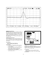
Definition : This is the time for the output voltage to return to
within a specified band around its voltage following a change
from full load to half load or half load to full load.
Test Parameter:
Measured Variable: Output Voltage Transients
Expected Results: Less than 50 usec (at 15 mV from
base line)
Test Procedure:
a. Connect the test equipment as shown in Figure A-4,
but replace the DVM with the oscilloscope. Operate
the electronic load in constant current mode.
b. Turn the supply's power on and turn CURRENT control fully clockwise.
c. Turn up output voltage to the full rated value.
d. Set the electronic load to transient operation mode
between one half of supply's full rated value and supply's full rated value at a 1 KHz rate with 50% duty
cycle.
e. Set the oscilloscope for ac coupling, internal sync and
lock on either the positive or negative load transient.
f. Adjust the oscilloscope to display transients as in Figure A-5.
g. Check that the pulse width of the transients at 15 mV
from the base line is no more than 50 usec as shown.
POWER SUPPLY
LOCAL
MASTER
Load Transient Response Time
UNDER TEST
M/S 1
CV
M/S 2
REMOTE
+
+S
SENSE
CC
SLAVE
-
+
-S
OUT
-
CV
+
-
CC
VREF A1 A2 A3 A4 A5
+
-
Rs
DIGITAL
VOLTMETER
TO
DVM
+
Model
-
+
ELECTRONIC
LOAD
E3614A, 15A, 16A
E3617A
Rs
0.1 ohm 0.1% 10W
1 ohm 1% 5W
Figure A-4. Basic Test Setup
A-4
Figure A-5. Load Transient Response Time Waveform
PARD(Ripple and Noise)
Definition: PARD is the Periodic and Random Deviation of
the dc output voltage from its average value, over a specified
bandwidth and with all other parameters maintained constant.
Constant voltage PARD is measured in the root-meansquare(rms) or peak-to-peak(pp) values over a 20 Hz to 20
MHz bandwidth. Fluctuations below the lower frequency limit
are treated as drift.
PARD(RMS) Measurement
The rms measurement is not an ideal representation of the
noise, since fairly high output noise spikes of short duration
could be present in the ripple and not appreciably increase
the rms value.
Test Parameter:
Measured Variable: Output Voltage(rms)
Expected Results: Less than 200 µV rms
Test Procedure:
a. Connect the test equipment as shown in Figure A-6.
b. Turn the supply's power on and turn CURRENT control fully clockwise.
c. Turn up output voltage to the full rated value. Check
that the supply's CV indicator remains lighted.
Reduce VOLTAGE control if not lighted.
d. Check that the rms noise voltage at the true rms voltmeter is less than 200BµV.
Figure A-6. CV PARD RMS Measurement Test Setup
PARD(Peak-to-Peak) Measurement
The peak-to-peak measurement is particularly important for
applications where noise spikes could be detrimental to a
sensitive load, such as logic circuitry.
Test Parameter:
Measured Variable: Output voltage(peak-to-peak)
Expected Results: Less than 1 mV p-p (20 Hz-20 MHz)
Test Procedure:
A-5
CONSTANT CURRENT (CC) TESTS
a. Connect the test equipment as shown in Figure A-7.
b. Turn the supply's power on and turn CURRENT control fully clockwise.
c. Turn up output voltage to the full rated value. Check
that the supply's CV indicator remains lighted.
Reduce VOLTAGE control if not lighted.
d. Set the oscilloscope to AC mode and bandwidth to 20
MHz.
e. Check that the peak-to-peak noise is less than 1 mV.
CC Setup. Constant current tests are analogous to constant
voltage tests, with the supply's output short circuited and the
voltage set to full output to assure CC operation. For output
current measurements the current monitoring resistor must
be treated as a four terminal device. Refer to the "Measurement Techniques" for details. All constant current measurements are made in terms of the change in voltage across this
resistor; the current performance is calculated by dividing
these voltage changes by ohmic value of Rs.
Load Regulation (Load Effect)
Definition: CC Load regulation is the change in the steady state
value of dc output current due to a change in load resistance
from short circuit to full load or from full load to short circuit.
Test Parameter:
Measured Variable: Output Current
Expected Results: Less than 0.01% plus 250 µA
Test Procedure:
a. Connect the DVM across Rs in Figure A-4. Operate
the electronic load in constant voltage mode and set
its voltage to the full rated value of power supply.
b. Turn the supply's power on and turn VOLTAGE control fully clockwise.
c. Turn up output current to the full rated value. Check
that the AMPS display reads full rated values and CC
indicator remains lighted. Reduce CURRENT control
if not lighted.
d. Record the voltage across Rs and convert it to current by dividing this voltage by Rs.
e. Operate the electronic load in short (input short)
mode.
f. When the reading settles, record voltage across Rs
again and convert it current. Check that the two
recorded readings differ less than 0.01% of output
current plus 250 µA.
Figure A-7.BCV PARD Peak-to-Peak Measurement Test
Setup
CV Drift (Stability)
Definition: The change in output voltage (dc to 20 Hz) for the
first 8 hours following a 30-minute warm-up period with constant input line voltage, constant load resistance and constant
ambient temperature.
Line Regulation (Source Effect)
Definition: Line regulation is the change in the steady state
value of dc output current due to a change in ac input voltage
from the minimum to maximum value(±10% of nominal voltage).
Test Parameter:
Measured Variable: Output Voltage
Expected Results: Less than 0.1% plus 5 mV
Test Procedure:
a. Connect the DVM across Rs in Figure A-4.
b. Operate the electronic load in constant current mode
and set its current to the full rated value of power supply.
c. Turn the supply's power on and turn CURRENT control fully clockwise.
d. Turn up output voltage to the full rated value as read
on the digital voltmeter.
e. After a 30-minute warm-up, note the voltage on DVM.
f. The output voltage reading should deviate less than
0.1% plus 5 mV from the reading obtained in step e
over a period of 8 hours.
Test Parameter:
Measured Variable: Output Current
Expected Results: Less than 0.01% plus 250 µA
Test Procedure:
a. Connect the DVM across Rs in Figure A-4. Operate
the electronic load in constant voltage mode and set
its voltage to the full rated value of power supply.
b. Connect the supply to the ac power line through a
variable autotransformer that set for low line voltage(104 Vac for nominal 115 Vac, 90 Vac for nominal
100 Vac, and 207 Vac for nominal 230 Vac).
c. Turn the supply's power on and turn VOLTAGE control fully clockwise.
d. Turn up output current to the full rated value. Check
that the AMPS display reads full rated values and CC
indicator remains lighted. Reduce CURRENT control
if not lighted.
A-6
CC Drift (Stability)
e. Record output voltage across Rs and convert it to
current by dividing this voltage by Rs.
f. Adjust autotransformer to the high line voltage (127
Vac for nominal 115 Vac, 110 Vac for nominal 100
Vac, and 253 Vac for nominal 230 Vac).
g. When the reading settles, record the voltage across
Rs again and convert it current. Check that the two
recorded readings differ less than 0.01% of output
current plus 250 µA.
Definition: The change in output current for the first 8 hours following a 30-minute warm-up with constant input line voltage,
constant load resistance and constant ambient temperature.
Test Parameter:
Measured Variable: Output Current
Expected Results: Less than 0.1% plus 10 mA
Test Procedure:
a. Connect the DVM across Rs in Figure A-4. Operate
the electronic load in constant voltage mode and set
its voltage to the full rated value of the power supply.
b. Turn the supply's power on and turn VOLTAGE control fully clockwise.
c. Turn up output current to the full rated value.
d. After a 30-minute warm-up, note the voltage on DVM
and convert it to current by dividing this voltage by Rs.
e. The converted output current should deviate less than
0.1% plus 10 mA from the current obtained in step d
over a period of 8 hours.
PARD(Ripple and Noise)
Definition : The residual ac current which is superimposed
on the dc output current of a power supply. Constant current
PARD is specified as the root-mean-square(rms) output current in a frequency range of 20 Hz to 20 MHz with the supply
in CC operation.
PARD(RMS) Measurement
Test Parameter:
Measured Variable: Output Current(rms)
Expected Results: E3614A: Less than 5 mA rms
E3615A: Less than 2 mA rms
E3616A: Less than 500 µA rms
E3617A: Less than 500 µA rms
Test Procedure:
a. Connect the test equipment as shown in Figure A-8.
b. Turn the supply's power on and turn VOLTAGE control fully clockwise.
c. Turn up output current to the full rated value. Check
that the CC indicator remains lighted. Reduce CURRENT control if not lighted.
d. Record rms voltage across Rs and convert it to current by dividing this voltage by Rs.
e. Check that the rms noise current is less than 5 mA
rms for E3614A, 2 mA rms for E3615A and 500 µA
rms for E3616A and E3617A respectively.
ADJUSTMENT AND CALIBRATION
PROCEDURE
Adjustment and calibration may be required after performance testing, troubleshooting, or repair and replacement.
Perform those adjustments that affect the operation of the
faulty circuit and no others. To remove the top cover, refer to
"Line Voltage Option Conversion" paragraph.
Maintenance described herein is performed with
power supplied to the supply, and protective covers
removed. Such maintenance should be performed
only service-trained personnel who are aware of the
hazards involved (for example, fire and electrical
shock). Where maintenance can be performed without power applied, the power should be removed.
Figure A-8. CC PARD RMS Measurement Test Setup
Figure A-9. Calibration Test Setup
A-7
Ammeter and CC Set Calibration
Overall Troubleshooting Procedure
To calibrate ammeter and CC set, proceed as follows:
a. Connect test setup on Figure A-9.
b. Turn VOLTAGE and CURRENT control fully clockwise.
c. Turn on the supply and to calibrate ammeter adjust
R5 on the display board until front panel AMPS display reads exactly DVM value divided by Rs.
d. To calibrate CC Set adjust R69 on the main board
until front panel AMPS display reads exactly DVM
value divided by Rs while depressing OVP/CC Set
switch.
To locate the cause of trouble follow steps 1, 2, and 3 in
sequence. Before attempting overall troubleshooting, ensure
that the rear-panel switches M/S 1 and M/S 2 be set to MASTER position and CV, CC, and SENSE to LOCAL position.
1. Check that input power is available, and check the
power cord and rear panel line fuse. When replacing
line fuse, be certain to select fuse of proper rating for
line voltage being used.
2. In almost all cases, the trouble source can be caused
by the dc bias or reference voltages; thus, it is a good
practice to check voltages in Table A-2 before proceeding with step 3.
3. Disconnect the load and examine Table A-3 to determine your symptom, then check the probable cause.
Voltmeter and OVP Set Calibration
To calibrate voltmeter and OVP set, proceed as follows:
a. Disconnect Rs from test setup on Figure A-9 and
connect DVM across output terminal of the supply.
b. Turn on the supply.
c. To calibrate voltmeter for E3614A, adjust R16 on the
display board until front panel VOLTS display reads
exactly DVM value. To calibrate voltmeter for
E3615A, E3616A and E3617A set the output voltage
below 18V (ex, 15V), and adjust R16 on the display
board until front panel VOLTS display reads exactly
DVM value. Next, set the output voltage above 20V
(ex, 21V) and adjust R17 on the display board until
front panel VOLTS display reads exactly DVM value.
d. To calibrate OVP Set, turn down the OVP Adjust
screwdriver control on the front panel slowly until the
OVP circuit trips. Record the output voltage when the
OVP trip occurs. Then adjust R97 on the main board
until front panel VOLTS display reads exactly OVP
trip voltage while depressing OVP/CC Set switch.
Reference and Bias Circuit
a. Make an ohmmeter check to be certain that neither
the positive and negative output terminal is grounded.
b. Turn front panel VOLTAGE and CURRENT controls
fully clockwise.
c. Turn on power supply (no load connected).
d. Proceed as instructed in Table A-2.
Regulating Loop Troubles
If the voltages in Table A-2 have been checked to eliminate
the reference and bias circuits as a source of trouble; the malfunction is caused by either the series regulator or preregulator feedback loop. Because the interaction between these two
loops makes logical troubleshooting difficult, the following
steps help you to locate the source of troubles in these two
feedback loops. Once the trouble has been located to one of
the feedback loops, the operation of either loop can be analyzed independently. This method should be followed whenever a low output voltage condition exists. Notice that
troubleshooting can proceed directly as described in Table A4 whenever a high output voltage condition exists.
1. Turn on the power supply with full load connected
and increase output voltage by turning up the front
panel voltage control. The output voltage is clamped
and CV indicator is turned off at some output voltage
(below full rated output voltage). If this is the case,
the series regulator feedback loop is operating
normally and the trouble condition is probably due to
a defect in the preregulator feedback loop (refer to
Table A-6). If the output voltage remains in low stage,
and varying the front panel voltage control has little or
no effect, then the trouble is probably in the series
regulator feedback loop. Refer to Table A-5.
2. Measure the voltage between TP2 and TP1 (shown
on the schematic diagram at the rear of the manual)
with full load with oscilloscope while increasing the
output voltage from 0 to full rated voltage. The voltage measured has step changes three times during 0
to full output voltage swing. If this is the case, preregulator feedback loop is operating normally. If this is
not the case, the trouble is probably in the preregulator feedback loop. Refer to Table A-6.
TROUBLESHOOTING
Before attempting to troubleshoot the power supply, ensure
that the fault is with the supply and not with an associated circuit. The performance test enables this to be determined
without having to remove the covers from the supply.
The applicable test points are identified by encircled
numbers on the schematic diagrams at the rear of the
manual, Figure A-10, Figure A-11, Figure A-12, and
Figure 13.
A good understanding of the principles of operation is a helpful aid in troubleshooting, and it is recommended that principles of operation in this manual be reviewed before
attempting to troubleshoot the supply. Once the principles of
operation are understood, refer to the overall troubleshooting
procedures paragraph to locate the symptom and probable
cause.
Once the defective component has been located (by means
of visual inspection or trouble analysis) replace it and reconduct the performance test. After a component is replaced,
perform the meter calibration.
A-8
After the trouble has been isolated to one of the feedback
loops, troubleshooting can proceed as described in Tables A4, A-5, or A-6.
series regulator backwards a stage at a time, since loop failures occur more often at the higher power levels.
Preregulator Feedback Loop. The preregulator feedback
loop (SCR control circuit) can be conveniently checked using
Table A-6. As indicated in Table A-6, the control circuit is
checked by starting with the waveform at point 7 and point 6
(shown on the schematic diagram) and tracing forwards and
backwards from this point.
Series Regulating Feedback Loop. When troubleshooting
the series regulating loop, it is useful to open the loop since
measurements made anywhere within a closed loop may
appear abnormal. With a loop closed, it is very difficult to separate cause from effect. As described in Tables A-4 and A-5,
the conduction or cutoff capability of each stage is checked
by shorting or opening a previous stage, as follows:
1. Shorting the emitter to collector of a transistor simulates saturation, or the full ON condition.
2. Shorting the emitter to base of a transistor cuts it off,
and simulates an open circuit between emitter and
collector.
Overvoltage Protection Circuit Troubles
When troubleshooting the overvoltage protection circuit, it is
useful to check the turn-on overshoot control circuit which
includes U20 and Q10. The function of the control circuit is to
slow down the rising speed of the +15 V bias the moment the
power is turned on. This function prevents the supply from
false OVP tripping the moment the power is turned on. After
the troubles has been isolated to overvoltage protection circuit, troubleshooting can proceed as described in Table A-7.
Although a logical first choice might be to break the loop
somewhere near its mid-point, and then perform successive
subdividing tests, it is more useful to trace the loop from the
Table A-2. Reference and Bias Circuit Troubleshooting
METER
COMMON
METER
POSITIVE
NORMAL INDICATION
NORMAL RIPPLE
(p-p)
PROBABLE CAUSE
TP6
point 2
+15.0 +/- 0.3 Vdc
2 mV
Check U13, CR31, and CR32.
TP6
point 4
-12.0 +/- 0.3 Vdc
2 mV
Check +15 V bias or U14.
TP6
TP7
+10.5 +/- 0.2 Vdc
2 mV
Check +15 V bias, U11, and U14.
TP6
point 3
-5.1 +/- 0.5 Vdc
2 mV
Check -12 V bias or VR1.
TP6
point 5
+5.0 +/- 0.3 Vdc
4 mV
Check U1 and CR2.
Table A-3. Overall Troubleshooting
SYMPTOM
CHECKS AND PROBABLE CAUSES
High Output Voltage
a. Check series regulator feedback loop or preregulator feedback loop.
b. Refer to "Regulating Loop Troubles" paragraph or Table A-4 or A-6 as instructed.
Low and No Output Voltage
a. If output is zero, check fuse.
b. Check series regulator feedback loop or preregulator loop.
Refer to "Regulating Loop Troubles" paragraph or Table A-5 or A-6 as instructed.
c. Check CR20 shorted.
High Ripple
a. Check operating setup for ground loops.
b. If output floating, connect 1 µF capacitor between output and ground.
c. Ensure that the supply is not crossing over to constant current mode
under loaded conditions.
d. Check for low voltage across C7 or Q1 and Q4.
e. Check for excessive ripple on reference voltages (Table A-2).
Poor Line Regulation
(Constant Voltage)
a. Check +10 V reference voltage.
b. Check U9.
A-9
Table A-3. Overall Troubleshooting (Cont’d)
SYMPTOM
CHECKS AND PROBABLE CAUSES
Poor Load Regulation
(Constant Voltage)
a. Refer to "Measurements Techniques" paragraph.
b. Check +10 V reference voltage.
c. Ensure that the supply is not going into current limit.
Poor Load Regulation
(Constant Current)
a. Check +10 V reference voltage.
b. CR1, CR19, CR20, C2, C31 leaky.
c. Ensure that the supply is not crossing over to constant voltage operation.
Oscillates (Constant Voltage/
Constant Current)
a. Check C29 and C36 in constant voltage circuit.
b. Check C31 and C33 in constant current circuit.
Poor Stability
(Constant Voltage)
a.
b.
c.
d.
Check +10 V reference voltage.
CR27, CR28, CR23, and CR26 leaky.
U9 defective.
Noisy programming resistor R83.
Poor Stability
(Constant Current)
a.
b.
c.
d.
Check +10 V reference voltage.
CR24, CR25, CR29, and CR30 leaky.
U9 and U10 defective.
Noisy programming resistor R85.
Excessive heat
a. Check preregulator control circuit. Refer to Table A-6.
b. CR10, CR12, CR15, and CR18 short
OVP Shutdown
a. Check that the front panel OVP Adjust screw control is rotated fully clockwise.
b. Check the overvoltage protection circuit.
Refer to "Overvoltage Protection Circuit Troubles" paragraph or Table A-7.
Table A-4. High Output Voltage Troubleshooting
STEP
ACTION
RESPONSE
PROBABLE CAUSE
1
Check turn off of Q1 and
Q4 by shorting Q9 emitter
to collector.
a. Output voltage remains high.
b. Output voltage decreases.
a. Q1 or Q4 shorted.
b. Remove short and proceed to step 2.
2
Check turn on of Q9 by
shorting point 1 to -12 V.
a. Output voltage remains high.
b. Output voltage decreases.
a. Q9 open.
b. Remove short and proceed to step 3.
3
Check voltage from pin 5
to pin 6 of U9.
a. Input voltage is positive.
b. Input voltage is negative.
a. U9B is defective.
b. Turn down the voltage control fully
counter clockwise. Check the voltage
of U9 pin 1 is 0.
Table A-5. Low Output Voltage Troubleshooting
STEP
ACTION
RESPONSE
PROBABLE CAUSE
1
Check turn on of Q1 and
Q4 by disconnecting emitter
of Q9.
a. Output voltage remains low.
b. Output voltage increases.
a. Q1 or Q4 open.
b. Reconnect emitter lead and proceed to step 2.
2
Check turn off of Q9 by
shorting point 1 to +15 V.
a. Output voltage remains low.
b. Output voltage increases.
a. Q9 shorted.
b. Remove short and proceed to step 3.
3
Eliminate constant current
comparator as a source of
trouble by disconnecting
anode of CR22.
a. Output voltage is increases.
b. Output voltage remains low.
a. Proceed to step 4.
b. Reconnect lead and proceed to step 5.
A-10
Table A-5. Low Output Voltage Troubleshooting (Cont’d)
STEP
ACTION
RESPONSE
PROBABLE CAUSE
4
Check voltage from pin 13 to
pin 12 of U9.
a. Measured voltage is positive.
b. Measured voltage is negative.
a. Check U9A is defective.
b. Check U10 and U9D is defective.
Check R85 is open.
5
Check voltage from pin 6
to pin 5 of U9.
a. Measured voltage is positive.
b. Measured voltage is negative.
a. U9B is defective.
b. Check U9C is defective.
Table A-6. Preregulator/Control Circuit Troubleshooting
STEP
MEASURE
RESPONSE
1
Set output voltage to 4.5 V +- 0.5 V for E3614A.
Set output voltage to 10 V +- 1 V for E3615A.
Set output voltage to 15 V +- 1 V for E3616A.
Set output voltage to 26 V +- 5 V for E3617A.
2
E3614A
E3615A
Waveform form from
TP6(common) to point 6
a. Normal firing pulse
b. No firing pulse
E3616A
Voltage from TP6
(common) to point 6
a. High voltage (+0.7 V)
PROBABLE CAUSE
a. Check CR18, CR15, Q7, Q8
for defective.
b. Proceed to step 3.
b. Low voltage (0 V)
a. CR15, CR18, U2, U21
defective
b. Proceed to step 3.
3
Voltage from TP6(common) to
U4 pin 1
a. Low voltage (-12 V)
b. High voltage (+5 V)
a. U3 defective
b. Proceed to step 4.
4
Voltage from TP6(common) to
U5 pin 1
a. High voltage (+15 V)
b. Low voltage (-12 V)
a. U4 defective
b. Proceed to step 5.
5
Voltage from pin 6 to
pin 7 of U5
a. Measured voltage is positive.
b. Measured voltage is negative.
a. U5 defective
b. U6 defective
6
Set output voltage to 7 V +- 1 V for E3614A.
Set output voltage to 16 V +- 2 V for E3615A.
Set output voltage to 25 V +- 2 V for E3616A.
Set output voltage to 44 V +- 5 V for E3617A.
7
Waveform form from TP6
(common) to point 7
a. Normal firing pulse
b. No firing pulse
a. CR10, CR12, Q5, Q6
defective
b. Proceed to step 8.
8
Voltage from TP6(common)
to U4 pin 14
a. Low voltage (-12 V)
b. High voltage (+5 V)
a. U3 defective
b. Proceed to step 9.
9
Voltage from TP6(common)
to U5 pin 14
a. High voltage (+15 V)
b. Low voltage (-12 V)
a. U4 defective
b. Proceed to step 10.
10
Voltage from pin 8 to
pin 9 of U5
a. Measured voltage is positive.
b. Measured voltage is negative.
a. U5 defective
b. U6 defective
A-11
Table A-7. Overvoltage Protection Circuit Troubleshooting
STEP
ACTION
RESPONSE
PROBABLE CAUSE
1
Short U19 pin 4 to TP6.
a. Shutdown release
(OVP indicator OFF)
b. Output voltage remains
shutdown(0 V)
a. U20 defective or C57
shorted.
b. Proceed to step 2.
2
Measure the voltage from
TP6(common) to TP9.
a. High voltage (+5 V)
b. Low voltage (0 V)
a. U19 defective or proceed step 3.
b. U4D defective.
3
Measure the voltage from
TP6(common) to TP8.
a. Below +2.6 V
b. Above +2.6 V
a. U12 or U8 defective
b. U18 defective
Table A-8. Reference Designators
REPLACEABLE PARTS
A
C
CR
DS
F
G
J
L
Q
R
S
T
TP
VR
U
W
INTRODUCTION
This section contains information for ordering replacement
parts. Table A-10 lists parts by reference designators and provides the following information:
a.
b.
c.
d.
e.
f.
Reference designators. Refer to Table A-8.
Agilent Technologies Part Number.
Total quantity used in that assembly.
Description.
Manufacturer's supply code number. Refer to Table
A-9 for manufacturer's name and address.
Manufacturer's part number or type.
Mechanical and miscellaneous parts are not identified by reference designator.
Assembly
Capacitor
Diode
Signaling Device(light)
Fuse
Pulse Generator
Jack
Inductor
Transistor
Resistor
Switch
Transformer
Test Point
Zener Diode
Integrated Circuit
Wire
ORDERING INFORMATION
To order a replacement part, address order or inquiry to your local Agilent Technologies sales office (see lists at rear of this manual for
addresses). Specify the following information for each part: Model, complete serial number of the power supply; Agilent Technologies
part number; circuit reference designator; and description.
Table A-9. Code List of Manufacturers
CODE
MANUFACTURER
ADDRESS
01295
Texas Instruments Inc, Semicon Comp Div.
Dallas, TX
14936
General Instruments Corp, Semicon Prod
Hicksville, N.Y.
27014
National Semiconductor Corporation
Santa Clara, CA
28480
Agilent Technologies
Palo Alto, CA
04713
Motorola Semiconductor Products
Phoenix, AZ
32997
Bourns Inc.
Riverside, CA
34371
Harris Corp.
Melbourne, FL
A-12
Table A-10. Replaceable Parts List
Reference Designator
R84,85
Agilen Part
Number
Q'ty
Description
Model
Mfr. P/N
Mfr.
Code
E3614A
1
60W BENCH POWER SUPPLY - E3614A MODEL
E3615A
1
60W BENCH POWER SUPPLY - E3615A MODEL
E3616A
1
60W BENCH POWER SUPPLY - E3616A MODEL
E3617A
1
60W BENCH POWER SUPPLY - E3617A MODEL
E3614-60005
1
MAIN BODY ASSY
14
28480
E3615-60005
1
MAIN BODY ASSY
15
28480
E3616-60005
1
MAIN BODY ASSY
16
28480
E3617-60005
1
MAIN BODY ASSY
17
28480
0371-3806
1
KEY CAP - WHT
ALL
28480
0371-8624
1
KEY CAP - GRAY
ALL
28480
E361X-60003
1
FRONT PANEL ASSY
ALL
28480
E361X-60009
1
DISPLAY BOARD ASSY
ALL
28480
2100-4503
2
RES-VAR 10K 5% 10-TURN WW
ALL
3590S-A17-103 32997
E3631-20011
1
BINDING POST RED
ALL
28480
E3631-20012
1
BINDING POST BLACK
ALL
28480
E3631-20013
1
BINDING POST GREEN
ALL
28480
2950-0144
3
NUT- BINDING POST
ALL
28480
5041-8621
2
KNOB
ALL
28480
E3614-60002
1
MAIN BOARD ASSY
14
28480
E3615-60002
1
MAIN BOARD ASSY
15
28480
E3617-60002
1
MAIN BOARD ASSY
16
28480
E3617-60002
1
MAIN BOARD ASSY
17
28480
5021-8128
1
PCB MAIN FOR E3614A,E3615A
14,15
28480
5021-8139
1
PCB MAIN FOR E3616A,E3617A
16,17
28480
C1,3,47
0160-4835
3
CAP-FXD .1UF +-10% 50V CER X7R
ALL
28480
C2
0180-4360
1
CAP-FXD 1000UF 25V +-20% AL-ELECTLT
14
28480
C2
0180-4355
1
CAP-FXD 470UF 50V +-20% AL-ELECTLT
15
28480
C2
0180-4452
1
CAP-FXD 330UF 63V +-20% AL-ELECTLT
16
28480
C2
0180-3595
1
CAP-FXD 220UF 100V +-20% AL-ELECTLT
17
28480
C4,5
0160-0269
2
CAP-FXD 0.1UF +-20% 500V CER Z5U
ALL
28480
C6
0180-3990
1
CAP-FXD 4700UF +-20% 25V AL-ELECTLT
ALL
28480
C7,8
0180-4567
2
CAP-FXD 39000UF 25V +-20% AL-ELECTLT
14
28480
C7,8
0180-4568
2
CAP-FXD 12000UF 63V +-20% AL-ELECTLT
15
28480
C7,8
0180-4607
2
CAP-FXD 5600UF 100V +-20% AL-ELECTLT
16
28480
C7,8
0180-4566
2
CAP-FXD 2700UF 160V +-20% AL-ELECTLT
17
28480
C9,41,42,43,55
0180-3970
5
CAP-FXD 1UF +-20% 50V AL-ELECTLT
ALL
28480
C10,48,49
0160-7449
3
CAP-FXD 0.33UF +-10% 50V POLYE-FL
ALL
28480
C11,16,17,25,26
0160-4832
5
CAP-FXD 0.01UF +-10% 100V CER X7R
14,15
28480
C12
0160-4835
1
CAP-FXD .1UF +-10% 50V CER X7R
14,15
28480
C13,14,15,30,32,
34,38,39,50,54
0160-4832
10
CAP-FXD 0.01UF +-10% 100V CER X7R
ALL
28480
A-13
Table A-10. Replaceable Parts List (Cont'd)
Reference Designator
Agilent Part
Number
Q'ty
Description
Model
Mfr. P/N
Mfr.
Code
C18,21,24,27
0160-7077
4
CAP-FXD .1UF +-10% 630V POLYE-FL
14,15
28480
C19,22
0160-4822
2
CAP-FXD 1000PF +-5% 100V CER COG
14,15
28480
C20,23
0180-3970
2
CAP-FXD 1UF +-20% 50V AL-ELECTLT
14,15
28480
C28
0160-6225
1
CAP-FXD 0.33UF +-10% 250V POLYE-MET
ALL
28480
C29
0160-4832
1
CAP-FXD 0.01UF +-10% 100V CER X7R
14,15
28480
C29
0160-7673
1
CAP-FXD .047UF +-10% 100V POLYP-MET
16,17
28480
C31
0160-7075
1
CAP-FXD 4700PF +-2% 50V POLYP-FL
ALL
28480
C33,35,44,45,46,
56
0160-4822
6
CAP-FXD 1000PF +-5% 100V CER COG
ALL
28480
C36
0160-7548
1
CAP-FXD 2200PF +-10% 50V CER Y5P
ALL
28480
C37
0160-4801
1
CAP-FXD 100PF +-5% 100V CER COG
ALL
28480
C40
0160-7673
1
CAP-FXD .047UF +-10% 100V POLYP-MET
ALL
28480
C52
0180-4085
1
CAP-FXD 330UF +-20% 35V AL-ELECTLT
ALL
28480
C53
0180-4355
1
CAP-FXD 470UF 50V +-20% AL-ELECTLT
ALL
28480
C57
0180-4437
1
CAP-FXD 47UF +-20% 50V AL-ELECTLT
ALL
28480
C58
0160-4065
1
CAP-FXD 0.1UF +-20% 250V PPR-MET
ALL
28480
C59,60
0160-7049
2
CAP-FXD 4700PF +-20% 250V CER X5V
ALL
28480
C61
0160-7363
1
CAP-FXD 1UF +-10% 250V POLYP-MET
16,17
28480
C62
0160-4808
1
CAP-FXD 470PF +-5% 100V CER COG
16,17
28480
C63,64,65,66
0160-0301
4
CAP-FXD 0.012UF +-10% 200V PE-FL
17
28480
R1,2
0811-3478
2
RESISTOR 0.1 +-1% 5W PWN TC=0+-90
14
28480
R1,2
0811-3839
2
RESISTOR 0.2 +-1% 5W PWN TC=0+-90
15
28480
R1,2
0811-3864
2
RESISTOR 0.6 +-5% 5W PWN TC=0+-90
16
28480
R1,2
0811-3861
2
RESISTOR 1.78 +-1% 5W PWN TC=0+-90
17
28480
R3,7,21,22,105,
106
0698-3160
6
RESISTOR 31.6K +-1% .125W TF TC=0+-100
ALL
28480
R4,71,73,76,112
0757-0465
5
RESISTOR 100K +-1% .125W TF TC=0+-100
ALL
28480
R5,6,80
0757-0401
3
RESISTOR 100 +-1% .125W TF TC=0+-100
ALL
28480
R8,9,12
0757-0280
3
RESISTOR 1K +-1% .125W TF TC=0+-100
14,15
28480
R8,9
0761-0021
2
RESISTOR 1K +-5% 1W TF TC=0+-100
16,17
28480
R10,108
0699-2715
2
RESISTOR-FUSE 1OHM +-5%; 0.5W @70
ALL
28480
R11
0811-1806
1
RESISTOR 2K +-5% 3W PWI 20PPM
14
28480
R11
0811-2188
1
RESISTOR 5K +-5% 3W PWI 20PPM
15
28480
R11
0764-0007
1
RESISTOR 27K +-5% 2W MO TC=0+-200PPM
16
28480
R11
0699-3105
1
RESISTOR 45K +-5% 2W MO TC=0+-500PPM
17
28480
R13
0757-0461
1
RESISTOR 68.1K +-1% .125W TF TC=0+-100
14,15
28480
R14,48,52
0698-3157
3
RESISTOR 19.6K +-1% .125W TF TC=0+-100
14,15
28480
R15
0757-0442
1
RESISTOR 10K +-1% .125W TF TC=0+-100
14,15
28480
R16
0757-0465
1
RESISTOR 100K +-1% .125W TF TC=0+-100
14,15
28480
R17,18,66,78,110, 0757-0280
123
6
RESISTOR 1K +-1% .125W TF TC=0+-100
ALL
28480
R19,113
0698-0083
2
RESISTOR 1.96K +-1% .125W TF TC=0+-100
ALL
28480
R20,23
0757-0463
2
RESISTOR 82.5K +-1% .125W TF TC=0+-100
ALL
28480
A-14
Table A-10. Replaceable Parts List (Cont'd)
Reference Designator
Agilent Part
Number
Q'ty
Description
Model
Mfr. P/N
Mfr.
Code
R24,26,27,37,38,
64,88,117,120
0757-0442
9
RESISTOR 10K +-1% .125W TF TC=0+-100
ALL
28480
R25,30,33
0698-8824
3
RESISTOR 562K +-1% .125W TF TC=0+-100
ALL
28480
R28,111
0698-3228
2
RESISTOR 49.9K +-1% .125W TF TC=0+-100
ALL
28480
R29,68,86,89,91,
92,95,96,99,114,
121
0698-3162
11
RESISTOR 46.4K +-1% .125W TF TC=0+-100
ALL
28480
R31,32,35
0698-0084
3
RESISTOR 2.15K +-1% .125W TF TC=0+-100
ALL
28480
R34
0757-0288
1
RESISTOR 9.09K +-1% .125W TF TC=0+-100
ALL
28480
R36
0698-3518
1
RESISTOR 7.32K +-1% .125W TF TC=0+-100
14
28480
R36
0757-0439
1
RESISTOR 6.81K +-1% .125W TF TC=0+-100
15
28480
R36
0757-0441
1
RESISTOR 8.25K +-1% .125W TF TC=0+-100
16
28480
R36
0698-8580
1
RESISTOR 9.53K +-1% .125W TF TC=0+-100
17
28480
R39
0757-0440
1
RESISTOR 7.5K +-1% .125W TF TC=0+-100
14
28480
R39
0698-4471
1
RESISTOR 7.15K +-1% .125W TF TC=0+-100
15
28480
R39
0698-3498
1
RESISTOR 8.66K +-1% .125W TF TC=0+-100
16
28480
R39
0757-0442
1
RESISTOR 10K +-1% .125W TF TC=0+-100
17
28480
R40
0757-0431
1
RESISTOR 2.43K +-1% .125W TF TC=0+-100
14
28480
R40
0698-4438
1
RESISTOR 3.09K +-1% .125W TF TC=0+-100
15
28480
R40
0698-0063
1
RESISTOR 5.23K +-1% .125W TF TC=0+-100
16
28480
R40
0757-0439
1
RESISTOR 6.81K +-1% .125W TF TC=0+-100
17
28480
R41
0698-4473
1
RESISTOR 8.06K +-1% .125W TF TC=0+-100
14
28480
R41
0757-0454
1
RESISTOR 33.2K +-1% .125W TF TC=0+-100
15
28480
R41
0698-4503
1
RESISTOR 66.5K +-1% .125W TF TC=0+-100
16
28480
R41
0757-0467
1
RESISTOR 121K +-1% .125W TF TC=0+-100
17
28480
R42,44,54,56
0757-0346
4
RESISTOR 10 +-1% .125W TF TC=0+-100
14,15
28480
R42,44,54,56
0698-3438
4
RESISTOR 147 +-1% .125W TF TC=0+-100
16,17
28480
R43,55
0757-0293
2
RESISTOR 1.96K +-1% .125W TF TC=0+-100
16,17
28480
R43,45,55,57
0757-0401
4
RESISTOR 100 +-1% .125W TF TC=0+-100
14,15
28480
R46,53
0757-0489
2
RESISTOR 10 +-1% .25W TF TC=0+-100
14,15
28480
R47,50
0698-4123
2
RESISTOR 499 +-1% .125W TF TC=0+-100
14,15
28480
R49,51
0757-0293
2
RESISTOR 1.96K +-1% .125W TF TC=0+-100
14,15
28480
R58,59
0811-3909
2
RESISTOR 0.2 +-1% 10W PWN TC=0+-90
14
28480
R58
0811-3909
1
RESISTOR 0.2 +-1% 10W PWN TC=0+-90
15
28480
R58
0811-4118
1
RESISTOR 0.6 +-1% 10W PWN TC=0+-90
16
28480
R58,59
0811-3861
2
RESISTOR 1.78 +-1% 5W PWN TC=0+-90
17
28480
R60
0811-1799
1
RESISTOR 390 +-5% 3W PWI TC=0+-20
14
28480
R60
0813-0001
1
RESISTOR 1K +-5% 3W PWI TC=0+-20
15
28480
R60
0811-0071
1
RESISTOR 1.52K +-5% 3W PWI TC=0+-20
16
28480
R60
0811-1808
1
RESISTOR 2.6K +-5% 3W PWI TC=0+-20
17
28480
R61
0698-0085
1
RESISTOR 2.61K +-1% .125W TF TC=0+-100
ALL
28480
R62
0698-7634
1
RESISTOR 42.2K +-1% .125W TF TC=0+-100
14
28480
R62
0698-4514
1
RESISTOR 105K +-1% .125W TF TC=0+-100
15
28480
R62
0757-0481
1
RESISTOR 475K +-1% .125W TF TC=0+-100
16
28480
A-15
Table A-10. Replaceable Parts List (Cont'd)
Reference Designator
Agilent Part
Number
Q'ty
Description
Model
Mfr. P/N
Mfr.
Code
R62
0698-8826
1
RESISTOR 825K +-1% .125W TF TC=0+-100
17
28480
R63
0698-8827
1
RESISTOR 1M +-1% .125W TF TC=0+-100
ALL
28480
R65
0757-0274
1
RESISTOR 1.21K +-1%.125W TF TC=0+-100
ALL
28480
R67
0757-0438
1
RESISTOR 5.11K +-1% .125W TF TC=0+-100
ALL
R69
2100-4306
1
RESISTOR-TRMR 50K 10% TKF TOP-ADJ 25-T
ALL
R70
0698-3243
1
RESISTOR 178K +-1% .125W TF TC=0+-100
14
28480
R70
0698-3459
1
RESISTOR 383K +-1% .125W TF TC=0+-100
15
28480
R70
0698-3158
1
RESISTOR 23.7K +-1% .125W TF TC=0+-100
16
28480
R70
0757-0465
1
RESISTOR 100K +-1% .125W TF TC=0+-100
17
28480
R72
0757-0289
1
RESISTOR 13.3K +-1% .125W TF TC=0+-100
14
28480
R72
0757-0290
1
RESISTOR 6.19K +-1% .125W TF TC=0+-100
15
28480
R72
0757-0458
1
RESISTOR 51.1K +-1% .125W TF TC=0+-100
16
28480
R72
0698-8123
1
RESISTOR 26.1K +-1% .125W TF TC=0+-100
17
28480
R74,75
0757-0444
2
RESISTOR 12.1K +-1% .125W TF TC=0+-100
14,15
28480
R74,75
0698-3245
2
RESISTOR 20.5K +-1% .125W TF TC=0+-100
16
28480
R74,75
0698-3136
2
RESISTOR 17.8K +-1% .125W TF TC=0+-100
17
28480
R77
0698-3430
1
RESISTOR 21.5 +-1% .125W TF TC=0+-100
14,15
28480
R77
0757-0395
1
RESISTOR 56.2 +-1% .125W TF TC=0+-100
16,17
28480
R79
0698-4767
1
RESISTOR 147K +-1% .125W TF TC=0+-100
14
28480
R79
0698-3460
1
RESISTOR 422K +-1% .125W TF TC=0+-100
15
28480
R79
0698-8825
1
RESISTOR 681K +-1% .125W TF TC=0+-100
16
28480
R79
0698-8827
1
RESISTOR 1M +-1% .125W TF TC=0+-100
17
28480
R81,122
0698-3157
2
RESISTOR 19.6K +-1% .125W TF TC=0+-100
ALL
28480
R82
0698-8123
1
RESISTOR 26.1K +-1% .125W TF TC=0+-100
14,15
28480
R82
0757-0461
1
RESISTOR 68.1K +-1% .125W TF TC=0+-100
16,17
28480
R83,119
0757-0440
2
RESISTOR 7.5K +-1% .125W TF TC=0+-100
ALL
28480
R87
0698-3444
1
RESISTOR 316 +-1% .125W TF TC=0+-100
ALL
28480
R90
0757-0346
1
RESISTOR 10 +-1% .125W TF TC=0+-100
ALL
28480
R93
0698-3581
1
RESISTOR 13.7K +-1% .125W TF TC=0+-100
ALL
28480
R94
2100-4357
1
RESISTOR-VAR 10K +-10%
ALL
52UAL-T22-A15 32997
R97
2100-4305
1
RESISTOR-TRMR 10K 10% TKF TOP-ADJ 25-T
ALL
3296Y-1-103
R98
0698-3455
1
RESISTOR 261K +-1% .125W TF TC=0+-100
14
28480
R98
0757-0465
1
RESISTOR 100K +-1% .125W TF TC=0+-100
15
28480
R98
0757-0461
1
RESISTOR 68.1K +-1% .125W TF TC=0+-100
16
28480
R98
0698-3160
1
RESISTOR 31.6K +-1% .125W TF TC=0+-100
17
28480
R100
0698-4123
1
RESISTOR 499 +-1% .125W TF TC=0+-100
ALL
28480
R101
0698-3441
1
RESISTOR 215 +-1% .125W TF TC=0+-100
ALL
28480
R102
0698-3438
1
RESISTOR 147 +-1% .125W TF TC=0+-100
ALL
28480
R103
0757-0428
1
RESISTOR 1.62K +-1% .125W TF TC=0+-100
ALL
28480
R104,107
0698-3156
2
RESISTOR 14.7K +-1% .125W TF TC=+-100
ALL
28480
R109
0698-3153
1
RESISTOR 3.83K +-1% .125W TF TC=0+-100
ALL
28480
R115
0757-0462
1
RESISTOR 75K +-1% .125W TF TC=0+-100
14
28480
A-16
28480
3296Y-1-503
32997
32997
Table A-10. Replaceable Parts List (Cont'd)
Reference Designator
Agilent Part
Number
Q'ty
Description
Model
Mfr. P/N
Mfr.
Code
R115
0757-0463
1
RESISTOR 82.5K +-1% .125W TF TC=0+-100
15
28480
R115
0757-0462
1
RESISTOR 75K +-1% .125W TF TC=0+-100
16
28480
R115
0757-0461
1
RESISTOR 68.1K +-1% .125W TF TC=0+-100
17
28480
R116
0698-4489
1
RESISTOR 28K +-1% .125W TF TC=0+-100
14
28480
R116
0698-3161
1
RESISTOR 38.3K +-1% .125W TF TC=0+-100
15,16
28480
R116
0698-4494
1
RESISTOR 35.7K +-1% .125W TF TC=0+-100
17
28480
R118
0698-8678
1
RESISTOR 178 +-1% .125W TF TC=0+-100
ALL
28480
R124
0698-8812
1
RESISTOR 1 +-1% .125W TF TC=0+-100
16,17
28480
R125
0698-8825
1
RESISTOR 681K +-1% .125W TF TC=0+-100
16,17
28480
R126
0757-0401
1
RESISTOR 100 +-1% .125W TF TC=0+-100
ALL
28480
U1
1826-0144
1
IC V RGLTR-FXD-POS 4.8/5.2V TO-220 PKG
ALL
U2
1826-0346
1
IC OP AMP GP DUAL 8 PIN DIP-P
14,15 LM358N
27014
U3,16,20
1826-0412
3
IC COMPARATOR PRCN DUAL 8 PIN DIP-P
ALL
LM393N
27014
U4,5
1826-0138
2
IC COMPARATOR GP QUAD 14 PIN DIP-P
ALL
LM339
27014
U6,9
1826-0665
2
IC OP AMP LOW-BIAS-H-IMPD QUAD 14 PIN
ALL
LF347BN
27014
U7,15,17
1826-1297
3
IC V RGLTR-V-REF-FXD 4.8/5.2V TO-92 PKG
ALL
LM336BZ-5.0
27014
U8
1990-1659
1
OPTO-ISOLATOR LED-TRIAC IF=100MA-MAX
ALL
MCP3020Z
14936
U10
1826-1702
1
IC OP AMP PRCN 8 PIN DIP-P
ALL
U11
1826-1075
1
IC OP AMP GP DUAL 8 PIN DIP-P
ALL
LF442CN
27014
U12
1826-0468
1
IC V RGLTR-OV-V-SEN 2.3/37.8V 8-DIP-P
ALL
MC3423P1
04713
U13
1826-0393
1
IC V RGLTR-ADJ-POS 1.2/37V TO-220 PKG
ALL
LM317T
27014
U14
1826-0221
1
IC V RGLTR-FXD-NEG -11.5/-12.5V TO-220
ALL
MC7912CT
04713
U18
1826-0346
1
IC OP AMP GP DUAL 8 PIN DIP-P
ALL
LM358N
27014
U19
1820-1197
1
IC GATE TTL/LS NAND QUAD 2-INP
ALL
SN74LS00N
01295
U21,22,23,24
1990-1659
4
OPTO-ISOLATOR LED-TRIAC IF=100MA-MAX
16,17 MCP3020Z
Q1,4
1855-0989
2
TRANSISTOR MOSFET N-CHAN E-MODE TO 247AC 14,15 IRFP044
28480
Q1,4
1855-0536
2
TRANSISTOR MOSFET N-CHAN E-MODE TO-3 SI
28480
Q2,3,10,11
1854-0477
4
TRANSISTOR NPN 2N2222A SI TO-18 PD=500MW ALL
2N2222A
04713
Q5,6,7,8
1854-0477
4
TRANSISTOR NPN 2N2222A SI TO-18 PD=500MW 14,15 2N2222A
04713
Q6,7
1853-0281
2
TRANSISTOR PNP 2N2907A SI TO-18 PD=400MW 16,17 2N2907A
04713
Q9
1853-0041
1
TRANSISTOR PNP SI TO-39 PD=1W FT=60MHZ
ALL
MM5007
04713
CR1,19
1901-1273
2
DIODE-PWR RECT 100V 6A 35NS
ALL
FE6B
14936
CR2
1906-0284
1
DIODE-FW BRIDGE 100V 1A
ALL
DF01
14936
CR3,4,5,6,7
1901-0033
5
DIODE-GEN PRP 180V 200MA DO-35
14,15 1N645
27014
CR8,9,16,17,31,32 1901-1149
6
DIODE-PWR RECT 400V 1A 50NS DO-41
ALL
UF4004
14936
CR10,12,15,18,20
1884-0332
5
THRYSTER-SCR TO-220AB VRRM=200V
ALL
MCR264-4
04713
CR11,14
1901-1149
2
DIODE-PWR RECT 400V 1A 50NS DO-41
14,15 UF4004
14936
CR13
1906-0400
1
DIODE-BRIDGE 600V 6A
ALL
14936
A-17
MC7805CT
04713
28480
16,17
GBU8J
14936
Table A-10. Replaceable Parts List (Cont'd)
Reference Designator
Agilent Part
Number
Q'ty
Description
Model
Mfr. P/N
Mfr.
Code
CR21,22,23,24,25, 1901-0033
26,27,28,29,30
10
DIODE-GEN PRP 180V 200MA DO-35
ALL
1N645
27014
VR1,2,3
1902-0579
3
DIODE-ZNR 5.1V 5% PD=1W IR=10UA
ALL
1N4733APL
04713
RT1,2
0837-0261
2
DIODE-VARISTOR
ALL
V275LA20A
34371
C67
0160-0263
1
CAP-FXD 0.22uF +-20% 50V CER
ALL
T1
9100-5068
1
TRANSFORMER-POWER
14
28480
T1
9100-5069
1
TRANSFORMER-POWER
15
28480
T1
NO P/N
1
TRANSFORMER-POWER
16
28480
T1
9100-5070
1
TRANSFORMER-POWER
17
28480
T2,3
9100-4969
2
TRANSFORMER-PULSE; PRI IND:5MH
14,15
28480
L1
9170-0894
1
CORE-SHIELDING BEAD
ALL
28480
MAGNETIC DEVICE
MISCELLANEOUS
J1
1252-4159
1
CONNECTOR-POST TYPE 2.5-PIN-SPCG 11-CO- ALL
NT
28480
TP1-16
0360-2359
16
TERMINAL-TEST POINT .230IN ABOVE
ALL
28480
S1,2,3,4
3101-3237
4
SWITCH-SL SPDT SUBMIN 6A 250VAC
ALL
28480
S5
3101-3238
1
SWITCH-SL DPDT SUBMIN 6A 250VAC
ALL
28480
S6
3101-1914
1
SWITCH-SL 2-DPDT STD 1.5A 250VAC PC
ALL
28480
S7
3101-3115
1
SWITCH-PB MOM .5A 250VAC
ALL
28480
S8
3101-3083
1
SWITCH-PB DPSTALTNG 6A 250VAC
ALL
28480
0360-2548
3
TERMINAL BLOCK
ALL
28480
0360-2545
1
TERMINAL BLOCK
ALL
28480
0360-2546
9
TERMINAL BLOCK
ALL
28480
0360-2547
1
TERMINAL BLOCK
ALL
28480
A-18
Table A-11. Component Value
Model
Component
E3614A
E3615A
E3616A
E3617A
C2
1000UF 25V +-20% AL-ELECTLT
470UF 50V +-20% AL-ELECTLT
330UF 50V +-20% AL-ELECTLT
220UF 100V +-20% AL-ELECTLT
C7,8
39000UF 25V +-20% AL-ELECTLT
12000UF 63V +-20% AL-ELECTLT
5600UF 100V +-20% AL-ELECTLT
2700UF 160V +-20% AL-ELECTLT
C11,16,17,25,26 0.01UF 100V +-10% CER X7R
0.01UF 100V +-10% CER X7R
C12
0.1UF 50V +-10% CER X7R
0.1UF 50V +-10% CER X7R
C18,21,24,27
0.1UF 630V +-10% POLYE-FL
0.1UF 630V +-10% POLYE-FL
C19,22
1000PF 100V +-5% COG
1000PF 100V +-5% COG
C20,23
1UF 50V +-20% AL-ELECTLT
1UF 50V +-20% AL-ELECTLT
C29
0.01UF 100V +-10% CER X7R
0.01UF 100V +-10% CER X7R
0.047UF 100V +-10% POLYP-MET
0.047UF 100V +-10% POLYP-MET
C61
1UF +-10% 250V POLYP-MET
1UF +-10% 250V POLYP-MET
C62
470PF +-5% 100V CER COG
470PF +-5% 100V CER COG
C63,64,65,66
0.012UF +-10% 200V PE-FL
R1,2
0.1 +-1% 5W
0.2 +-1% 5W
0.6 +-5% 5W
1.78 +-1% 5W
R8,9
1K 1% .125W
1K 1% .125W
1K +-5% 1W
1K +-5% 1W
R11
2K +-5% 3W
5K +-5% 3W
27k +-5% 2W
45K +-5% 2W
R12
1K +-1% .125W
1K +-1% .125W
R13
68.1K +-1% .125W
68.1K +-1% .125W
R14,48,52
19.6K +-1% .125W
19.6K +-1% .125W
R15
10K +-1% .125W
10K +-1% .125W
R16
100K +-1% .125W
100K +-1% .125W
R36
7.32K +-1% .125W
6.81K +-1% .125W
8.25K +-1% .125W
9.53K +-1% .125W
R39
7.5K +-1% .125W
7.15K +-1% .125W
8.66K +-1% .125W
10K +-1% .125W
R40
2.43K +-1% .125W
3.09K +-1% .125W
5.23K +-1% .125W
6.81K +-1% .125W
R41
8.06K +-1% .125W
33.2K +-1% .125W
66.5K +-1% .125W
121K +-1% .125W
R42,44,54,56
10 +-1% .125W
10 +-1% .125W
147 +-1% .125W
147 +-1% .125W
R43,55
100 +-1% .125W
100 +-1% .125W
1K +-1% .125W
1K +-1% .125W
R45,57
100 +-1% .125W
100 +-1% .125W
R46,53
10 +-1% .25W
10 +-1% .25W
R47,50
499 +-1% .125W
499 +-1% .125W
R49,51
1.96K +-1% .125W
1.96K +-1% .125W
R58
0.2 +-1% 10W
0.2 +-1% 10W
0.6 +-1% 10W
1.78 +-1% 5W
R59
0.2 +-1% 10W
R60
390 +-5% 3W
1K +-5% 3W
1.52K +-5% 3W
2.6K +-5% 3W
R62
42.2K +-1% .125W
105K +-1% .125W
475K +-1% .125W
825K +-1% .125W
R70
178K +-1% .125W
383K +-1% .125W
23.7K +-1% .125W
100K +-1% .125W
R72
13.3K +-1% .125W
6.19K +-1% .125W
51.1K +-1% .125W
26.1K +-1% .125W
R74,75
12.1K +-1% .125W
12.1K +-1% .125W
20.5 +-1% .125W
17.8K +-1% .125W
R77
21.5 +-1% .125W
21.5 +-1% .125W
56.2 +-1% .125W
56.2 +-1% .125W
R79
147K +-1% .125W
422K +-1% .125W
681K +-1% .125W
1M +-1% .125W
R82
26.1K +-1% .125W
26.1K +-1% .125W
68.1K +-1% .125W
68.1K +-1% .125W
R98
261K +-1% .125W
100K +-1% .125W
68.1K +-1% .125W
31.6K +-1% .125W
R115
75K +-1% .125W
82.5K +-1% .125W
75K +-1% .125W
68.1K +-1% .125W
R116
28K +-1% .125W
38.3K +-1% .125W
38.3K +-1% .125W
35.7K +-1% .125W
R124
1 +-1% .125W
1 +-1% .125W
R125
681K +-1% .125W
681K +-1% .125W
MOSFET N-CHAN E-MODE TO 3 SI
MOSFET N-CHAN E-MODE TO 3 SI
PNP 2N2907A SI TO-18 PD=400MW
PNP 2N2907A SI TO-18 PD=400MW
OPTO-ISOLATOR LED-TRIAC
OPTO-ISOLATOR LED-TRIAC
TRANSFORMER-POWER FOR E3616A
TRANSFORMER-POWER FOR E3617A
1.78 +-1% 5W
Q1,4
MOSFET N-CHAN E-MODE TO 204AE
MOSFET N-CHAN E-MODE TO 204AE
Q5,8
NPN 2N2222A SI TO-18 PD=500MW2
NPN 2N2222A SI TO-18 PD=500MW
Q6,7
NPN 2N2222A SI TO-18 PD=500MW2
NPN 2N2222A SI TO-18 PD=500MW2
U2
IC OP AMP GP DUAL 8 PIN DIP-P
IC OP AMP GP DUAL 8 PIN DIP-P
CR3,4,5,6,7
DIODE-GEN PRP 180V 200MA D0-35
DIODE-GEN PRP 180V 200MA D0-35
CR11,14
DIODE-PWR RECT 400V 1A 50NS DO-41 DIODE-PWR RECT 400V 1A 50NS DO-41
T1
TRANSFORMER-POWER FOR E3614A
TRANSFORMER-POWER FOR E3615A
T2,3
TRANSFORMER-PULSE; PRI IND:5MH
TRANSFORMER-PULSE; PRI IND:5MH
U21,22,23,24
A-19
Manual Supplement
Supplement Agilent Part Number : 5959-5336, Edition 4
Supplement Print Date : 14 April, 2000
This supplement updates the following document:
Agilent E361XA 60W Series Lab Bench DC Power Supplies
Manual Agilent Part Number : 5959-5310
What is a manual supplement?
A manual supplement keeps your manual up-to-date. The supplement, which
consists of additional pages for your manual, is shipped with the manual that it
updates. Additional pages have page numbers with a lower-case letter. For
example, if one additional page is added between pages 1-10 and 1-11, it will be
numbered 1-10-1.
This supplement is new information that was not described in the manual
for remote programming of the E3614A/E3615A/E3616A/E3617A with a voltage
or current source and resistors.
Voltage and Current Programming of the E3614A/15A/16A/
17A with a Voltage and Current Source
Remote analog voltage programming permits control of the regulated output voltage
or current by means of a remotely varied voltage or current. The stability of the
programming voltages directly affects the stability of the output. The voltage control
or current control on the front panel are disabled during analog programming.
NOTE
The CV(-) terminal on the rear panel is internally connected to the plus output
terminal. In following connections, it is recommended to use Figure 2, Figure 4, or
Figure 6 if the negative terminal of the “Programming Voltage” is not floted from
its circuits.
Constant Voltage Mode
The programming voltage is not isolated from the power supply output. The power
supply may be programmed with a voltage that is common to either the plus output,
or the minus output.
Programming Voltage Common to the Plus output
Figure 1
Set the CV switch down on the rear panel, and all others up.
Vin = 1/A x Vout
Vout = A x Vin
Where
Vout is the power supply output voltage.
Vin is the programming voltage.
A is the gain factor and the values of each model are as below.
Model
A
1/A
E3614A
0.8
1.25
E3515A
2.0
0.5
E3616A
3.5
0.29
E3617A
6.0
0.17
1-10-1
Programming Voltage Common to the Minus Output
Figure 2
Set the CV switch down on the rear panel, and all others up.
Vin = 1/A x Vout
Vout = A x Vin
Where
Vout is the power supply output voltage.
Vin is the programming voltage.
A is the gain factor and the values of each model are as below.
Model
A
1/A
E3614A
0.44
2.25
E3515A
0.67
1.5
E3616A
0.78
1.29
E3617A
0.86
1.17
Alternative Voltage Programming Using Resistors
Programming Voltage Common to the Plus Output
Figure 3
The M/S2 switch must be in the down position. For best results, place a 0.1µF capacitor in
parallel with R2.
Vin = (R1/R2) x Vout
Vout = (R2/R1) x Vin
Where
Vout is the power supply output voltage.
Vin is the programming voltage.
R1 and R2 should be in the 1KΩ to 100KΩ range.
1-10-2
Programming Voltage Common to the Minus Output
Figure 4
The output will always be the same or less than the programming voltage.
The M/S2 switch must be in the down position. For best results, place a 0.1µF capacitor
in parallel with R2.
Vin = (R1R2) / R2 x Vout
Vout = R2 / R1+R2) x Vin
Where
Vout is the power supply output voltage.
Vin is the programming voltage.
R1 and R2 should be in the 1KΩ to 100KΩ range.
1-10-3
Constant Current Mode
The E3614A/15A/16A/17A may be programmed for constant current with an analog
voltage or current. Constant current with analog voltage programming can only be
achieved with a voltage source that is common with the positive output terminal.
Constant Current with Voltage Programming
Figure 5
Set the CC switch down the rear panel, and all others up.
Vin = 1/A x Iout
Iout = A x Vin
Where
Iout is the power supply output current.
Vin is the programming voltage.
A is the transconductance in Amp/Volt and the values of each
model are as below.
Model
A (A/V)
1/A (V/A)
E3614A
0.6
1.67
E3515A
0.3
3.33
E3616A
0.17
6.0
E3617A
0.1
10
Constant Current with Current Programming
When using current to program the power supply, the source must have a
dynamic range of 10 volts when the programming source is common to the plus
output and 10 volts plus the maximum output voltage expected when the
programming source is common to the minus output of the power supply.
The load to the power supply must be stable for the constant current
output to be accurate. Current transient response is not specified,
and depends on the change of the output voltage of the power supply.
1-10-4
Figure 6
Set the CC switch down, and all others up.
Iin = 1/A x Iout
Iout = A x Vin
Where
Iout is the power supply output current in amps.
Iin is the programming current in µamps.
A is the gain.
A (A/µA)
Model
1/A (µV/A)
E3614A
0.055
18
E3515A
0.0278
35.9
E3616A
0.0158
63.4
E3617A
0.00928
108
Programming currents can be increased by adding a resistor across the CC+ and CC-. A
10 volts drop across R1 represents full scale current of the power supply. When a 1 kohm
resistor is added across R1, the programming currents are as follows with the
programming current in mA.
Model
A (A/mV)
Parallel resistor required for a
1 amp/mamp value of A (kohm)
1/A (mA/A)
E3614A
0.594
1.69
1.7
E3515A
0.297
3.37
3.45
E3616A
0.168
5.95
6.28
E3617A
0.0989
1.01
11.2
Current Monitoring
Current of the power supply can be monitored across the internal current monitoring
resistor. One side of the resistor is at the +output and A3; the other side of the resistor
is at A1. The table below shows the resistor value and conversion factors. To obtain
the current divide the measured voltage by the resistor value or multiply the amps/V
times the voltage measured.
Resistor
value (Ω)
Model
amps/V
E3614A
0.1
10
E3515A
0.2
5
E3616A
0.6
1.67
E3617A
0.89
1.12
1-10-5
Voltage and Current Programming of the
E3614A/15A/16A/17A with Resistors
Remote programming with resistors permits control of the regulated output or current
by means of a remotely varied resistor. The sum of the resistance of external
programming resistors (R1 + R2) should be more than 40 kohm. To have more precise
output voltage, use a variable resistor more than 40 kohm. The voltage control on the
front panel is disabled during remote resistor programming.
NOTE
Do not operate the power supply simultaneously in the remote analog voltage
programming and in the remote resistor programming.
Remote Resistor Programming Connections
Remote resistor programming requires changing the setting of the switches and
connecting external resistors between “+” and “`-” terminals of “CV” and “VREF”
terminal or “+” and “-” terminals of “CC” and “VREF” terminal. Any noise picked up
on the programming leads will appear on the power supply's output and may degrade
regulation. To reduce noise pickup, use a twisted or shielded pair of wires for
programming, with the shield grounded at one end only.
Remote Resistor Programming, Constant Voltage
Figure 7
Set the CV switch down on the rear panel, and all others up.
Vout = A x [VREF x {R/(R + R2 + 100)}]
Where
Vout is the power supply output voltage.
A is the gain factor and the values of each model are as below.
VREF is between 10.11 V and 11.40 V.
R = (92800 x R1)/(92800 + R1)
R1 + R2 > 40 kohm
Model
A
E3614A
0.8
E3515A
2.0
E3616A
3.5
E3617A
6.0
1-10-6
Remote Resistor Programming, Constant Current
Figure 8
Set the CC switch down on the rear panel, and all others up.
Iout = A x [VREF x {R/(R + R2 + 100)}]
Where
Iout is the power supply output current.
A is the gain factor and the values of each model are as below.
VREF is between 10.11 V and 11.40 V.
R = (92800 x R1)/(92800 + R1)
R1 + R2>> 40 kohm
Model
A
E3614A
0.6
E3515A
0.3
E3616A
0.17
E3617A
0.1
1-10-7
I
CERTIFICATION
Agilent Technologies certifies that this product met its published specifications at time of shipment from the factory. Agilent
Technologies further certifies that its calibration measurements are traceable to the United States National Institute of Standards and Technology (formerly National Bureau of Standards), to the extent allowed by that organization's calibration facility,
and to the calibration facilities of other International Standards Organization members.
WARRANTY
This Agilent Technologies hardware product is warranted against defects in material and workmanship for a period of three
years from date of delivery. Agilent software and firmware products, which are designated by Agilent for use with a hardware
product and when properly installed on that hardware product, are warranted not to fail to execute their programming instructions due to defects in material and workmanship for a period of 90 days from date of delivery. During the warranty period,
either Agilent or Agilent Technologies will, at its option, either repair or replace products which prove to be defective. Agilent
does not warrant that operation the software, firmware, or hardware shall be uninterrupted or error free.
For warranty service, with the exception of warranty options, this product must be returned to a service facility designated by
Agilent. Return to Englewood Colorado Service Center for repair in United States(1-800-258-5165). Customer shall prepay
shipping charges by (and shall pay all duty and taxes) for products returned to Agilent for warranty service. Except for the
products returned to Customer from another country, Agilent shall pay for return of products to Customer.
Warranty services outside the country of initial purchase are included in Agilent's product price, only if Customer pays Agilent
international prices (defined as destination local currency price, or U.S. or Geneva Export price).
If Agilent is unable, within a reasonable time, to repair or replace any product to condition as warranted, the Customer shall
be entitled to a refund of the purchase price upon return of the product to Agilent.
The warranty period begins on the date of delivery or on the date of installation if installed by Agilent.
LIMITATION OF WARRANTY
The foregoing warranty shall not apply to defects resulting from improper or inadequate maintenance by the Customer, Customer-supplied software or interfacing, unauthorized modification or misuse, operation outside of the environmental specifications for the product, or improper site preparation and maintenance. TO THE EXTENT ALLOWED BY LOCAL LAW, NO
OTHER WARRANTY IS EXPRESSED OR IMPLIED. AND AGILENT SPECIFICALLY DISCLAIMS THE IMPLIED WARRANTIES OF MERCHANTABILITY AND FITNESS FOR A PARTICULAR PURPOSE.
For consumer transactions in Australia and New Zealand:
The warranty terms contained in this statement, except to the extent lawfully permitted, do not exclude, restrict or modify and
are in addition to the mandatory rights applicable to the sale of this product to you.
EXCLUSIVE REMEDIES
TO THE EXTENT ALLOWED BY LOCAL LAW, THE REMEDIES PROVIDED HEREIN ARE THE CUSTOMER'S SOLE AND
EXCLUSIVE REMEDIES. AGILENT SHALL NOT BE LIABLE FOR ANY DIRECT, INDIRECT, SPECIAL, INCIDENTAL, OR
CONSEQUENTIAL DAMAGES, WHETHER BASED ON CONTRACT, TORT, OR ANY OTHER LEGAL THEORY.
ASSISTANCE
The above statements apply only to the standard product warranty. Warranty options, extended support contacts, product
maintenance agreements and customer assistance agreements are also available. Contact your nearest Agilent Technologies Sales and Service office for further information on Agilent's full line of Support Programs.
DECLARATION OF CONFORMITY
According to ISO/IEC Guide 22 and CEN/CENELEC EN 45014
Manufacturer’s Name and Addresss
Responsible Party
Agilent Technologies, Inc.
550 Clark Drive, Suite 101
Budd Lake, New Jersey 07828
USA
Alternate Manufacturing Site
Agilent Technologies (Malaysia) Sdn. Bhd
Malaysia Manufacturing
Bayan Lepas Free Industrial Zone, PH III
11900 Penang,
Malaysia
Declares under sole responsibility that the product as originally delivered
Product Name:
a) Single Output dc Power Supply (dual range)
b) Single Output dc Power Supply (single range)
c) Single Output System Power Supply
d) Multiple Output dc Power Supply
e) Multiple Output System dc Power Supply
Model Number:
a) E3610A, E3611A, E3612A
b) E3614A, E3615A, E3616A, E3617A
c) E3632A
d) E3620A, E3630A
e) E3631A
Product Options:
This declaration covers all options of the above product(s).
Complies with the essential requirements of the Low Voltage Directive 73/23/EEC and the EMC
Directive 89/336/EEC (including 93/68/EEC) and carries the CE Marking accordingly .
EMC Information
ISM Group 1 Class A Emissions
As detailed in
Electromagnetic Compatibility (EMC), Certificate of Conformance Number
CC/TCF/00/102 based on Technical Construction File (TCF) ANJ12, dated
Dec.20, 2000.
Assessed by:
Celestica Ltd, Appointed Competent Body
Westfields House, West Avenue
Kidsgrove, Stoke-on-Trent
Straffordshire, ST7 1TL
United Kingdom
Safety Information
and Conforms to the following safety standards.
IEC 61010-1:2001 / EN 61010-1:2001
CSA C22.2 No. 1010.1:1992
This DoC applies to above-listed products placed on the EU market after:
January 1, 2004
Date
Bill Darcy/ Regulations Manager
For further information, please contact your local Agilent Technologies sales office, agent or distributor, or
Agilent Technologies Deutschland GmbH, Herrenberger Straβe 130, D71034 Böblingen, Germany
Revision: B.00.00
Issue Date: Created on 11/24/2003 3:10
PM
Document No. KIO_10-32.11.24doc.doc