1
EK -RlV 12-UG-002
RLV12
Disk Controller
User's Guide
RLV12
Disk Controller
User's Guide
Prepared by Educational Services
of
Digital Equipment Corporation
.
1st Edition, July 1981
2nd Printing (Rev), March 1982
Copyright © 1981, 1982 by Digital Equipment Corporation
All Rights Reserved
The material in this manual is for informational purposes and is subject to change without notice.
Digital Equipment Corporation assumes no responsibility for any errors which may appear in this manual.
Printed in U.S.A.
This document was set on DIGITAL's DECset-8000 computerized
typesetting system.
The following are trademarks of Digital Equipment
Corporation:
DIGITAL
DEC
PDP
DECUS
UNIBUS
DECLAB
D ECsystem -10
DECSYSTEM-20
DIBOL
EduSystem
VAX
VMS
MASSBUS
OMNIBUS
OS/8
RSTS
RSX
lAS
MINC-Il
7/82-15
CONTENTS
CHAPTER 1
INTRODUCTION
1.1
1.2
1.3
1.3.1
1.3.2
DESCRIPTION .....................................................................................................
FEATURES ...........................................................................................................
SPECIFIC.lL\TIONS...............................................................................................
RL V 12 Disk Controller..................................................................................
RLOI/RL02 Disk Drives................................................................................
CHAPTER 2
FUNCTIONAL DESCRIPTION
2.1
2.2
2.3
2.4
2.4.1
2.4.2
2.4.3
2.4.4
2.6.1
2.6.2
2.7
2.8
2.9
INTRODUCTION.................................................................................................
BUS PROTOCOL..................................................................................................
BUS TRANSCEIVERS ........................................................................... '" .... .......
PROGRAMMABLE REGISTERS ......................................................................
Bus Address Register (BAR)..........................................................................
Bus Address Extension Register (BAE) .........................................................
Disk Address Register (DAR) ........................................................................
Control/Status Register (CSR) ...... ................................................................
MUltipurpose Register (MPR) .......................................................................
FIFO Memory, FIFO Serializer and Word Difference Counter ...................
DATA SOURCE MULTIPLEXER AND CRC GENERATOR ........................
MICROSEQUENCER, CONTROL STORE PROMS,
AND BUFFER REGISTER ..................................................................................
Buffer Register Fields .....................................................................................
Fatal Error Clearing Logic .............................................................................
CONTROL REGISTERS AND PULSE GENERATORS .................................
WRITE ENCODER AND PRECOMPENSATION LOGIC .............................
DATA SEPARATOR READ CIRCUIT ..............................................................
CHAPTER 3
CONFIGURATION AND INSTALLATION
3.1
3.2
3.3
3.4
3.S
3.6
3.7
3.8
3.9
INTRODUCTION.................................................................................................
DEVICE ADDRESS SELECTION......................................................................
BUS SELECTION .................................................................................................
INTERRUPT VECTOR........................................................................................
INTERRUPT REQUEST LEVEL .......................................................................
MEMORY PARITY ERROR ABORT FEATURE.............................................
JUMPERS THAT REMAIN INSTALLED ........................................................
INSTALLATION ..................................................................................................
ACCEPTANCE TESTING ...................................................................................
CHAPTER 4
REGISTERS
4.1
4.2
4.3
4.4
4.4.1
4.4.2
4.4.3
INTRODUCTION .................................................................................................
CONTROL/STATUS REGISTER (CSR) ...........................................................
BUS ADDRESS REGISTER (BAR)....................................................................
DISK ADDRESS REGISTER (DAR) .................................................................
DAR During a Seek Command ......................................................................
DAR During a Read, Write, or Write Check Command ...............................
DAR During a Get Status Command.............................................................
2.4.S
2.4.6
2.S
2.6
111
1-1
1-1
1-1
1-1
1-3
2-1
2-3
2-4
2-4
2-S
2-S
2-S
2-7
2-8
L-'J
2-10
2-10
2-11
2-11
2-12
2-12
2-1S
3-1
3-1
3-1
3-2
3-2
3-4
3-4
3-S
3-S
4-1
4-1
4-1
4-4
4-4
4-4
4-4
CONTENTS (Coot)
4.5
4.5.1
4.5.2
4.5.3
4.6
MULTIPURPOSE REGISTER (MPR) ...............................................................
Writing the MPR to Set the Word Count.......................................................
Reading the MPR After a Read Header Command ......................................
Reading the MPR After a Get Status Command...........................................
BUS ADDRESS EXTENSION REGISTER (BAE) ...........................................
CHAPTER 5
COMMANDS
5.1
5.2
5.3
5.4
5.5
5.6
5.8
5.9
5.10
5.10.1
5.10.2
5.11
INTRODUCTION.................................................................................................
WRITE CHECK (1) ..............................................................................................
GET STATUS (2) ..................................................................................................
SEEK (3) ................................................................................................................
READ HEADER (4)..............................................................................................
WRITE DATA (5) .................................................................................................
READ DATA (6) ...................................................................................................
READ WITHOUT HEADER CHECK (7) ..........................................................
MAINTENANCE FUNCTION (0)......................................................................
EXAMPLES OF USING COMMANDS .............................................................
Seek Operation ...............................................................................................
Data Transfer Operation ................................................................................
ERROR RECOVERY ...........................................................................................
CHAPTER 6
DISK DRIVE
6.1
6.2
6.3
INTRODUCTION.................................................................................................
USER SWITCHES AND INDiCATORS............................................................
110/220 VOLTAGE AND NORMAL/LOW VOLTAGE
RANGE SETTING ...............................................................................................
5.7
4-4
4-4
4-7
4-7
4-7
5-1
5-1
5-1
5-2
5-2
5-2
5-2
5-2
5-3
5-3
5-4
5-4
5-5
6-1
6-2
6-2
TABLES
Table No.
2-1
3-1
4-1
4-2
4-3
4-4
4-5
4-6
5-1
5-2
6-1
Title
Control/Status Register Bits ..................................................................................
Address Selection....................................................................................................
CSR Word Format..................................................................................................
DAR Seek Command Word FormaL......................................................................
DAR Read/Write Data Command Word FormaL.................................................
DAR Get Status Command Word Format .............................................................
MPR Word Count Format ......................................................................................
MPR Status Word Format......................................................................................
Controller Status Errors..........................................................................................
Disk Drive Status Errors.........................................................................................
Voltage and Range Selector Setting .......................................................................
IV
Page
2-8
3-2
4-2
4-5
4-5
4-6
4-6
4-8
5-5
5-6
6-3
FIGURES
Figure No.
2-1
2-2
2-3
2-4
2-5
2-6
2-7
2-8
2-9
2-10
2-11
2-12
2-13
3-1
3-2
3-3
3-4
4-1
4-2
4-3
4-4
4-5
4-6
4-7
4-8
4-9
6-1
6-2
Title
RL V 12 Block Diagram ...........................................................................................
Bus Protocol Logic ..................................................................................................
Bus Transceivers .....................................................................................................
Bus Address Register (BAR) Circuit......................................................................
Bus Address Extension Register (BAE) Circuit .....................................................
Disk Address Register (DAR) Circuit....................................................................
Control/Status Register (CSR) Circuit..................................................................
FI Fa RAM, Buffers, and Serializer .......................................................................
Microsequencer, Control Store PROMs, and Buffer Register. ..............................
MFM Encoding .......................................................................................................
Peak Shift Waveform ..............................................................................................
Write Encoder and Precompensation Circuit .........................................................
Data Separator Read Circuit..................................................................................
RL V 12 Jumper Locations.......................................................................................
RL V 12 Device Address Format..............................................................................
RLV12 Interrupt Vector Format ............................................................................
RL V 12 Installation .................................................................................................
Control/Status Register (CSR) ..............................................................................
Bus Address Register (BAR) ..................................................................................
DAR During a Seek Command ..............................................................................
DAR During a Read, Write, or Write Data Command ..........................................
DAR During a Get Status Command .....................................................................
Writing the MPR to Set the Word Count...............................................................
Reading the MPR After a Read Header Command
(Three Header Words)............................................................................................
Reading the MPR After a Get Status Command ...................................................
BAE Register Word Format ...................................................................................
RLO 1jRL02 Disk Drive (Front View) ....................................................................
RLOljRL02 Disk Drive (Rear View).....................................................................
v
Page
2-2
2-3
2-4
2-5
2-6
2-6
2-7
2-9
2-10
2-12
2-13
2-14
2-15
3-3
3-4·
3-4
3-6
4-3
4-3
4-5
4-5
4-6
4-6
4-7
4-7
4-8
6-1
6-3
rHADT~R 1
'-...-.1.
.t"1..1.
.I. b I
.I.
INTRODUCTION
1.1 DESCRIPTION
The RL V 12 Disk Controller interfaces RLO 1 and RL02 disk drives to any quad- or hex-size backplane
that uses a 16-, 18-, or 22-bit LSI-II bus. One RL V12 controls up to four disk drives. The RL V 12
consists of one quad-size module (M806I), a BC80M cable, a drive terminator, and drive identification
hardware.
The RLO 1 and RL02 disk drives are random-access, mass-storage, subsystems that store data in fixedlength blocks on a preformatted disk cartridge. Each RLOI can store 5.24 million bytes, and each RL02
can store 10.48 million bytes. The drives are 26.67 cm (10.5 in) high, self-cooled, rack-mountable units
and come complete with a power supply. Option RLVI2-AK includes one RLOI drive, and option
RL V22-AK includes one RL02 drive.
The RLVI2 transfers data to and from the LSI-II bus using direct memory access (DMA)
tions. This allows data transfers to occur without first going to the processor.
1.2 FEATURES
The RL V 12 controller has the following features.
•
•
•
•
•
•
Single quad-size module; needs no C-D connections.
Supports DMA data transfers in 16-, 18-, or 22-bit addressing modes.
Software compatible with RL VII controller (16- or I8-bit mode only).
Supports 22-bit addressing on an LSI-II bus.
Controls from one to four RLO 1/RL02 drives.
Memory parity error abort feature for use with memories that have a parity option.
1.3 SPECIFICATIONS
1.3.1
RLV12 Disk Controller
Module
1 quad-size module, M806I
Size
Height: 26.56 cm (10.457 in)
\Vidth: 1.27 cm (0.5 in)
Length: 22.70 cm: (8.94 in)
Power Requirements
+ 5 Vdc
± 5% at 5.0 A
+12 Vdc ± 5% at 0.1 A
Bus Loads
ac bus loads
dc bus load
Addressing Modes
2.7
1
16-, 18-, and 22-bit (determined by user)
1-1
transac~
Minimum Configuration
for 22-Bit Address Mode
H9275-A or similar backplane that supports 22-bit addressing, and
memory capable of 22-bit addresses, such as the MSV II-L or the
MSVII-P.
Limitations
The RL V 12 will not fit in the dual-height LSI-II mini-series H9281
backplane.
Drives per Controller
Up to four RLOI and RL02 drives in any combination
LSI-II Bus-Addressable
Registers
8 (5 are used; 3 are not used)
Base Device Address
Selected by jumpers as follows.
Addressing Mode
Base Device Address
16-bit
18-bit
22-bit
1744008
7744008
177744008
Device I nterrupt Vector
0001608, jumper selectable
Data Transfer Rates
4.9
3.9
2.0
Error Detection Capability
~s/word
~s/word
~s/word
(avg) drive to controller, controller to memory
(peak) drive to controller
(peak) controller to memory
Cyclic redundancy check (CRC) on data and headers
Memory parity error abort for use with memories that have parity
checking
Maximum Cable Length
Controller to Last Drive
30 m (100 ft)
Environment Specifications
Temperature
Storage
Operating*
-40 0 C to 66 0 C (-40 0 F to 150 0 F)
50 C to 60 0 C (41 0 F to 11 0 0 F)
Relative Humidity
Storage
Operating
10% to 90%, noncondensing
10% to 90%, noncondensing
Altitude
Not operating
Operating*
9 km (5.6 mi) max
2.4 km (1.5 mi) max
Airflow
Operating
Max temperature rise across module must not exceed 10° C
(18 0 F) input to output.
* Reduce
the maximum operating temperature by 1.8 0 C for each 1000 m altitude above sea level or 10 F for each 1000 ft
above sea level.
1-2
1.3.2
RLOI/RL02 Disk Drives
Storage Type
Medium
Magnetic disk cartridge
Recording Surfaces
2 data surfaces
2 read/write heads
iVlagnetic heads
Recording Capacity (formatted)
Cylinders per cartridge
Tracks per cylinder
Tracks per cartridge
Sectors per track
Bytes per sector
Bytes per track
Bytes per cylinder
Bytes per cartridge
Recording Method
RLOI
RL02
256
2
512
40
256
10,240
20,480
5.24 M
512
2
1024
40
256
10,240
20,480
10.48 rv1
,-1" f" d 1.requency
f
. rno d U1.atlOn
. 1 • (MJ:'M'I
1. J
M Oulde
1
1.
1
Performance
Transfer Rate
40-sector (16-bit data words):
4.9 Jis/word (avg) drive to controller, controller to memory
3.9 Jis/word (peak) drive to controller
::.::.
_~
f~ •• ~\
JJ
111~
\Q.Vt,)
17 ms (one track)
100 ms (max)
Revolution Latency
12.5 ms (avg)
Operating Environment
Temperature Range
Relative Humidity
Wet Bulb Temperature
Altitude
Heat Dissipation
10° C to 40° C (50° F to 104°F) at sea level
10% to 90%, noncondensing
28° C (82° F) max
Up to 2400 m (8000 ft) at max temperature of 36° C (96° F)
150 W (546 Btu/hr)
Operation
Start Time
Stop Time
Revolutions per Minute
50 s
30 s
2400
1-3
Power
Drive
Single-phase
Starting Current
5 A (rms) max, 120 V, 47/63 Hz
2.5 A (rms) max, 240 V, 47/63 Hz
l\1echanical Drive
Size
48 cm wide X 63.4 cm deep X 27 cm high (19 in wide X 25 in
deep X 10.5 in high)
Weight
33.75 kg (75 Ib )
Mounting
The drive mounts on slides in a standard 48.26 cm (I9 in) cabinet
(provided). Recommended max height from floor is 18.9 cm (48
in).
Cartridge
Embedded servo
Top loading cartridge with 2 data surfaces.
Standard Cable Lengths
Power cord
2.74 m (9 ft)
Controller to First Drive
1.83 m (6 [t)
Drive to Drive
3.05 m (10 ft)
Optional Drive Cables
Cable
Part No.
Length
BC20J-20
BC20J-40
BC20J-60
7012122-20
7012122-40
7012122-60
6 m (20 ft)
12 m (40 [t)
18 m (60 [t)
NOTE
Total length of cable(s) from controller to the last
drive must not exceed 30 m (100 ft).
]-4
CHAPTER 2
FUNCTIONAL DESCRIPTION
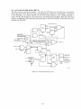
2.1 INTRODUCTION
The RL V 12 controller interfaces the RLO 1 and RL02 disk drives to a 16-, 18-, or 22-bit LSI-II bus.
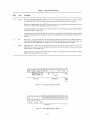
One RLV12 can support up to four RLOI and RL02 disk drives in any combination. The RLV12 module, M8061, has the LSI-II bus transceivers and decoders, programmable registers, the controller timing and sequence logic, and the data formatting circuits necessary to read and write on the disk.
The main sections of the RL V12 are shown in Figure 2-1. The RL V 12 has the following five programmable registers.
Control/status register (CSR)
Bus address register (BAR)
Disk address register (DAR)
Multipurpose register (MPR)
Bus address extension register (BAE) (22-bit addressing only)
These registers can be addressed like any memory location. The CSR is always written last of these five
registers because it starts the microsequencer operation.
An RLVI2 program can selectI6-, 18-, or 22-bit LSI-II bus addressing. When not enabled for 22-bit
addressing, the module is software compatible with and can replace the RLVII or RLV21.
NOTE
The RLV12 may be used in a 16- or IS-bit system
while configured to a 22-bit operation (factory shipped configuration) provided it is the only RLV12 in
the system.
To issue a command to the RL V 12, the processor first places the address of the register on the LSI-II
bus. Then it places the data on the bus. The RLV12 controller decodes the address and channels the
data to the correct register. The processor loads the bus address register (BAR) with bits 0 through 15.
H 18- or 22-bit addressing is used, the processor also loads the bus address extension register (BAE)
with bits 16 through 21. Bits 16 and 17 may also be written to or read from the control/status register
(CSR). The CSR is loaded in the same way.
Once the command is written into the control/status register, the RL VI2 starts a microsequencer routine. The microsequencer decodes the command and branches to an address in the control store
PROMs. There the microsequencer finds a routine for the command issued. The microsequencer then
generates the control signals needed to channel the data through the controller.
Included on the controller are error detection features, such as the memory parity error abort feature
for use with memories that have parity error checking. When reading system memory, data bits 16 and
17 from the bus are checked for a parity error. If an error is detected, the current command to the
controller is aborted.
2-1
6 ,1
"
, OR 22-BI T
~
-
BDAl
16,17
MEMORY
PARITY ERROR
ABORT LOGIC
I
PAR ERR
~
SET OPI_
OPI
ERROR
F/F
r-- DRI VE 1/0
FATAL ERR H
~ LSI -11 BUS
n
~
NXM
NXM
ERROR
lOGIC
BUS
DRIVE ERROR
DR ERR
DRIVE READY
DR ROY
°
DRIVE SElECTO
DR SEl
DRIVE SELECT 1
DRSEl1
ZERO l
-
CSR
~----------------~~
FUNCTION CMOS
~
MICROSEQUENCE R
ST A TUS FLAGS
CONTROL STORE
DATA lATE
BUFF ERR EG ISTE RS
•
'---
BUS
PROTOCOL
SEC P lS
SECTOR PULSE
r-___--'W--'R,;..T;..:E~G_A;.:.T.;:E_ _ _ _ _ _-I
r---S-Y~S:--T:--E-M-"'8.2
CONTROL REGISTERS
A,B,C, AND 0 PULSE
MUX SEl
GENERATORS,
(FIFO CONTROL,
ClK SEl
DATA PATH CONTROL
AND MUX SElECTI
CLOCK
8.2MHZ
--2-
WR GATE
MHZ
SYS1 H
1--
SYS ClK
(41 MHZ)
SYSO H
CRCERR
C RC CH ECK E R i 4 - - . - - - t - - - - - - - - e > i
GENERATOR
MS ClK
• A ... J\.
I' -
AND
A
"
./ ----- '\
'\ ADDRESS
~DECODER
~
¢=::) _
DAR
r----v<
REGISTER
ZERO BIT--'
v'
v~
_~
I
TS )7FIr-F_0_1_5_:0_0
_ _ _ _ _......,I./
......_____________
,~,,,
j I
......------"
BPOK
POWER
OK
BUFFER
CN'~
DS DATA
I
MUX DATA H
ClK SEl
CLOCK
MUX
i+--
MS ClK
8,2
~HZ
WR DATA
STATUS ClK
D~ _(SMS elK IMAINTI
DATA SEPARATOR
READ CIRCUIT
I (PHASE
WRITE ENCODERi+--
:
~..J...;."':J---'7-'-"-"-~'" ~ ~ ~~~ 0 N
WR DATA PlS
lOCK LOOPI
\-..c:R.;:D....:D:.;.A..,;..T'-CA-'--_ _ _ _ _ _ _--I
{\-_~S~T~A-'-T~U~S~IN_ _ _ _ _ _ _ _ _ _ _~---------------~
RD DATA
STATUS
MA~NT
READ STATUS
FSMI ClK
DIFFERENCE
COUN1ER
UP
(ON TRANSFER TO RAMI
SER
DATA IN
i
BIT~
MUX S E l -
SERIAlFIFO
IZER
/~-r----'
WORD
FIFO RAM
256 X 16
~lK
WRITE MARKER
IVlS
FIFO
FIFO
OUTPUT
~
INPUT
BU F FER I /I......__V
_____--I BU F FE R
7
SER DATA OUT SOURCE
.---+-.J.::.=:'';:';'D-'-S'-'D-'-A-=T'':A'-'+I M U l TIP lEX E R
SHIFT
,
-~
~_ _ _~_+_~_S_E_R_D_A~DATA
"DA 15:00V~
"
DR CMD
SEND DRIVE COMMAND
CRC
DISK
ADDRESS
BUS
TRANSCEIVERS
DR
CMD
F/F
WD FOUR (RD NPRI
CNt DN
(ON TRANSFER FROM RAMI
POK
Figure 2-1
RL V I 2 Block Diagram
PWRFAll
The RL V 12 has a 256 X 16-bit RA M to store data for or from direct memory access (0 MA) transactions. The RAM is a first-in, first-out (FIFO) memory that can store up to 256 words of data.
During a write command, a FIFO serializer is used with the FIFO RAM to convert parallel data into
serial format to be written on the disk. During a read command, the FIFO serializer converts the serial
data into parallel data to be loaded into the FIFO RAM.
2.2 BUS PROTOCOL
The bus protocol logic (Figure 2-2) generates the control signals to read from or write to the controller.
This logic uses a DC004 as a bus protocol chip. Two negative logic decoders and one positive logic
decoder provide the read and write signals to the five RL V 12 registers: CSR, BAR, DAR, MPR, and
BAE. The following events occur.
1.
At addressing time, R SYNC H clocks in the address bits (TSDAL 1, 2 and 3). These address bits are decoded to read or write to the five registers.
2.
The DC004 generates a slave reply signal, SRPL Y H, that becomes BRPL Y L to the processor and completes the LSI-II bus protocol.
ENADDLQ.
EN DAT L
XMIT H
TO BUS
TRANSCEIVERS
WRITE
DECODER
FROM
THREESTATE
BUS
D-TYPE
FLlPFLOPS
READ TO
REGISTERS
ILJ-"--+-+-+-It- R D CS R L
IL}----'--+--t--1~
R DBA R L
LJ-----'--+-t- R D DA R L
DECODER
TO
REGiSTERS
11 r1
WR CSR L
LJ------'L.- R D BAE L
WR CSR PLS H
WR BAR L
WR BAR PLS H
WR DAR L
WR DAR PLS H
vv~ !I.~!l~
TS DAL 3
ATCH
!...
WR BAE L
V'!R
~!!PR
PLS H
WR BAE PLS H
TS DAL 2
SEL
TS DAL 1
DATA
R SYNC H
CLK
EN
R DOUT L
WR PLS H
SEL
BRPLY
IN WD
DCOO4
CRDY H
MRPL Y L
D
CLK
S DEV EN H
BRPL Y L
TO LSI-ll BUS
IN WD L
-MASTER H
MASTER H
DSK WRT H
MRPLY H
TRANSCEIVERS
SINGLE RANK
SYNCHRONIZER
MR 5738
Figure 2-2
Bus Protocol Logic
2-3
3.
A single rank synchronizer monitors controller ready (CRDY) to enable the slave device (the
addressed register). MRPLY L clocks in CRDY and generates S DEV EN H.
4.
When CRDY is asserted, the RL V 12 is ready to accept another command.
5.
The signals XMIT Hand REC H go to the DCOOS transceivers that interface the LSI-II bus
and the 16-bit three-state DAL bus.
2.3 BUS TRANSCEIVERS
The bus transceivers on the RL V 12 are DCOOSs, as shown in Figure 2-3. These transceivers transmit
and receive both data and address information. They interface the LSI-II BDAL 0-15 H signals and
the RL V 12 TS DAL 0-15 H bus/address signals. BBS7 L must be asserted during address time to
enable the transceivers. The transceivers are controlled by the signals XMIT Hand REC H from the
bus protocol logic.
The jumper pins connected to the transceivers select the device address and the interrupt vector of the
RLVI2.
DC005
N/OUT
H
TO/FROM
LSI-11 BUS
DC005
}i8;:=:E~~TATEHN/OUT
BUS
TS DAL 11-14
}TSDAL89
" 10 , 15
J
J
MATCH H {
MATCH H
BDAL 8-10
BDAL "_'4{
BDAL15
BBS7 L
TO WIRE
WRAP PINS
ADDRESS
ADDRESS
TO WIRE
WRAP PINS
-RD BAE H
VECTOR
XMIT H
REC H
TO OTHER DC005
BUS TRANSCEIVERS
MR 5739
Figure 2-3
Bus Transceivers
2.4 PROGRAMMABLE REGISTERS
The five programmable registers of the RL V 12 interface to a three-state bus (TS DAL BUS). These
registers receive address, data, and control information, via the bus, and they return data and status
information on the same bus.
2-4
2.4.1 Bus Address Register (BAR)
The BAR (Figure 2-4) has two DC006 binary counters. The BAR is loaded with the 16-bit bus address
to which the first word of a DMA transfer is to be made. The signal WR BAR L enables the register to
load this address.
WR BAR L------..J'1I
X}---r--
SEL BAR
RD BAR L
BUS ADDRESS REGISTER
Dcaa6
Dcaa6
DUAL!
BIN
COUNTER
DUAL!
BIN
COUNTER
MAX-C H
SA
I - - I f - - - - - - - ( : J I SA
MAX A CRY H
L . . . - . . - - - - - - L J RD
RD
MAX C CRY H
r---~
CLK-A
CLK-C
CLK-C
WR MPR l
B INIT L
CLK-A
S-C
1--If-----+--4~
LD
1--If-----+--4:.11 LD
I
I
-SRPLYL=LjJ'
WCBARLD
R DOUT l
S-C
,
~
WC BAR ClK l
MR 5740
Figure 2-4
Bus Address Register (BAR) Circuit
2.4.2 Bus Address Extension Register (BAE)
The BAE (Figure 2-5) is a 6-bit register for the extended address bits, 16 through 21. For 22-bit addressing, the BAE is loaded from TS DAL 0-5 using a write BAE command.
For 18-bit addressing, the extended address bits 16 and 17 can be loaded either into BAE bits 0 and 1 or
into CSR bits 4 and 5.
NOTE
Writing CSR bits 4 and 5 modifies BAE bits 0 and 1
and vice versa.
2.4.3 Disk Address Register (DAR)
The DAR (Figure 2-6) holds the next sector address to read or write data on the disk. After each sector
is read or written, the contents of the DAR is incremented by 1. The output of the DAR goes to the
DAR serializer.
During a Seek command, the DAR is used for the head selected, the direction to travel, and the cylinder address difference. During a Read, Write, or Write Check command, the DAR is used for the head
selected, the next sector address to read or write, and the cylinder address. During a Get Status command, the DAR is used to get the drive status and to clear the drive error register of soft errors.
The DAR serializer has two 8-bit shift registers that load parallel data in and shift serial data out. The
DAR serializer sends the data to the header compare circuit.
2-5
BIN CNTR
TS OAL 5
0
BAE 21X H
TS OAL 4
0
BAE 20X H
TS OAL 3
0
BAE 19X H
2
0
BAE 18 X H
TS DAL
RO BAE L
00
WR BAE L
lOAD
WR BAE PlS H
ClK
....-+---------------1o
MUX
BAE
RSLT H
BIN
CNTR
t--""----t- BA E 17 X H
r-+-~-------------------~O
TS OAL 4
BAE 16X H
TS OAl
OH
0
WR CSR l
RO BAE L
TS DAL 0
TS DAL 5
0
TS OA.L 1
1
-VJR CSR H
"'-~-____,LOAO
CLK
L--J
WR BAE l
B
WR BAE PlS H
WR CSR PlS H
MAX-A H
!'viR 5741
Figure 2-5
Bus Address Extension Register (BAE) Circuit
FROM
THREE-STATE
BUS
TSOALO-15H
RO DAR l
DAR
SER OA H
SHFT lO
_M_S_C_l_K_H
___-1 C l K
lOA 0
INC DAR H
DAR
SERIAlIZER
OAO-15 H
00
--"--'--..;;:;....~
WR DAR PlS H
SHIFT
REGISTER
(1 OF 2)
BINARY
COUNTER
(1 OF 4)
MARKER H
-SER OA INH l
ClK
INHIBIT
MR 5742
Figure 2-6
Disk Address Register (DAR) Circuit
2-6
2.4.4 Control/Status Register (CSR)
The CSR (Figure 2-7) is a holding register for the command to the microsequencer. The register also
holds the interrupt enable bit, the controller ready signal, the drive select bits, and error flags. A command to read the CSR gets status information as shown in Table 2-1.
TS DAl 0
CSR
F1 H
TS DAl 2 H
FROM
THREESTATE
BUS
TS DAL 1
FO H
TS DAl 1 H
F2 H
TSDAl3H
IE H
TS DAl 6 H
TS DAL 2
DRSElOH
TSDAl8H
DR SEll H
TS DAL 9 H
ClK
TS DAL 7 H
WR CSR PLS H
TS DAL 3
I
I
TO
THREESTATE
BUS
CRDY H
0
PAR ERR L
F/F
Ie
0
OPI H
-CRDY H
TS DAL 10
OPI
F/F
K
D/H CRC H
TS DAL 11
DL T/HNF H
TS DAL 12
TIMER
RDAL16XH~
M25
WR CSR
RDAL17XH
DATA FROM
LSI-11 BUS
.n,)A
J
,.,..,/
550 MS
l
- - - - - - - - - - - - - - - ,
An
~ '''L~
= M23
r\O\'"
ERROR
F/F
EN ADD L
K
NXM
ONE
SHOT
NXM H
0
TS DAL 13
NXM
F/F
C
lOJ.1S
ERR H
RD CSR L
MR·5743
Figure 2-7
Control/Status Register (CSR) Circuit
When set by the hardware, the controller ready flip-flop indicates that the RL V 12 is ready to accept a
command. The CRDY bit in the CSR is cleared by software. After this bit is clear, the firmware-generated signal PLS OPI H starts the OPI watchdog timer.
The watchdog timer allows 550 ms for the controller to complete an instruction. The timer prevents the
controller from taking too much time to perform an instruction and keeping out other instructions. If
the instruction is not complete within 550 ms, the timer clocks the OPI flip-flop, enabling OPI H, which
turns off the controller.
2-7
Some of the CSR status error signals have two meanings depending on the state of the OPI flip-flop.
When the DjH CRC flag is set without OPI H set~ a data CRC error occurred; with OPI H set~ a
header CRC error occurred.
When the DL T jHNF flag is set without OPI H
header not found error occurred.
set~
a data late error occurred; with OPI H set, a
During a DMA transfer, the NXM one-shot allows 10 J.ls for·the addressed memory location to send and
return BRPL Y L. This one-shot prevents the RLV 12 from indefinitely holding the LSI-II bus. If the
one-shot times out~ it clocks the NXM flip-flop~ setting NXM H~ and releases the LSI-II bus.
If NXM H is set without OPI H set~ a nonexistent memory error occurred. If NXM H is set with OPI
H set, a memory parity error occurred. (A memory parity error forces both the NXM flip-flop and the
OPI flip-flop set.)
Any error that occurs also sets status bit 15.
Table 2-1
Control/Status Register Bits
CSR Bit(s)
Status Information
°
Drive ready (DRDY)
Command function code (FO, Fl, F2)
Extended address bits 16 and 17 (DAL 16-17)
Interrupt enable (IE)
Cuniruiit:r ready (CRDY)
Drive selected (DS)
Operation incomplete (OPI)
Data CRC error (DCRC)
Header CRC error (HCRC)
Data late (DL T)
Header not found (HNF)
Nonexistent memory (NXM)
Parity error abort (PAR ERR)
Drive error (DE)
Error flag (ERR)
1-3
4, 5
6
7
8, 9
10
II
10, II
12
10, 12
13
10, 13
14
15
2.4.5 lVlultipurpose Register (lVIPR)
The MPR has three functions and uses different circuits depending on the command being performed.
1.
Word Count Register - During a Read Data or Write Data command~ the MPR functions as
a word count (WC) register and uses the same circuit as the bus address register, shown in
Figure 2-4. Before either command is issued~ the number of words to be transferred (the word
count) is written into the MPR. The words transferred go through one of the FIFO buffers to
the FI Fa memory (see Paragraph 2.4.6). At the end of each sector read or written, the word
count is incremented. When the count is complete~ the word count overflow (MAX-C H In
Figure 2-4) clocks the word count flip-flop and ends the data transfer.
2.
Status Register - Following a Get Status command, the MPR functions as a status register.
The controller places the disk status information in the FI Fa output buffer, shown in Figure
2-8. The disk status word from the selected drive is placed in this buffer and can be read by
reading the MPR. (See Paragraph 4.5.3.)
2-8
3.
Memory Buffer Register - Following a Read Header command, the MPR functions as a
memory buffer register. The controller places the three header words in the FIFO memory.
Reading the MPR places the header words, one at a time, in the FIFO output buffer. To read
the three header words requires three successive read MPR instructions. (See Paragraph
II
~.
2.4.6
~
'"l \
.J.k.)
FIFO Memory, FIFO Serializer, and Word Difference Counter
The FI FO memory is a first-in, first-out 256 X 16-bit RAM that can store up to 256 data words. A
FIFO serializer takes serial data from the disk, makes it parallel, and places it in the FIFO memory.
The FIFO serializer also takes parallel data out of the FIFO memory, makes it serial, and sends it to
the disk. See Figure 2-8.
A word difference counter keeps track of the number of words coming from the disk to the FI FO buffer. After four words are read from the disk, the word difference counter signals the microsequencer to
start a D MA transaction.
RD FIFO EN l
I
I
ADDRESS
GENER- ~------I
ATOR
RAM ADD 0-7 H
RD MPR l
elK C
ClK A
SEl APT H
TS F I F 0 0-15 H
FROM
o PU lSE
GENERATORS
FIFO OUTPUT
BUFFER
FIFO INPUT
BUFFER
D-TYPE
F/F
is r i r G 0- i 5 i-i
THREE-STATE BUS
RD MPR H
RD MPR OUT l
EN OAT H
EN OUT
A MPR ClK OUT H ClK
RD MPR IN l
EN OUT
-,-T....::D..:...;IN-,--,-,-H- - - i C l K
DISK STATUS IN H
FROM CONTROL
REGISTER C
RD STATUS H
SER DATA IN H
-RD STATUS H
FIFO
SERIAlIZER
FROM DATA DS DATA H
SEPARATOR
DO/EVEN DATA
(SER DATA OUT)
TO DATA SOURCE
MULTIPLEXER
M R5744
Figure 2-8
FIFO RAM, Buffers, and Serializer
2-9
2.5 DATA SOURCE MULTIPLEXER AND CRC GENERATOR
Data that is to be written on the disk goes to a data source multiplexer (see Figure 2-1). MUX SEL 0,
1, and 2 determine which of the following inputs reaches the multiplexer output.
Serial Input
Source
SER DA (disk address)
SER DATA OUT
DS DATA
CRC
DAR (disk address register)
FIFO serializer
Data separator
CRC checker/generator
The multiplexer's serial output, MUX DATA H, goes to the write encoder precompensation circuit to
be written on the disk. At the same time, a CRC check word is being created by the CRC checker /generator. This check word is then added to the end of the data field of the sector.
When the header or sector is read from the disk, the data is again sent through the CRC checker /generator. Any errors in the data or in the CRC word are detected, and a data CRC (DCRC) or a
header CRC (HCRC) error bit is set in the control/status register.
2.6 MICROSEQUENCER, CONTROL STORE PROMS, AND BUFFER REGISTER
The microsequencer decodes the function commands of the CSR and points to an address in the control
store PROMs, where the routine resides, to execute the command. The microsequencer sends an address (PR ADD 0-9 H) to the control store PROMs. (See Figure 2-9.)
PR ADD 0-9
LD CTRL C
PR OUT 0-23
LD CTRL B
CONTROL
STORE
PROMS
BUFFER
REGISTER
- T FLAG X H
LD CTRL A
TO CONTROL
REGISTER A,B,C
AND PULSE 0
GENERATORS
T MUX SEL 0-2
CRDY H
DEVSELH
INSTR 0-4
T MUX SEL
RE L
CONDITIONAL
BRANCH
LOGIC
FE L
SO H
S1 H
SEL
FLAGS
1\JIR 5745
Figure 2-9
Microsequencer, Control Store PROMs. and Burrer Register
2-10
The control store PROMs receive the address from the microsequencer and generate a 24-bit microinstruction at the outputs (PR OUT 0-23 H). The PROM outputs go to a buffer register, which is
divided into five fields as follows.
1.
2.
3.
4.
5.
Instruction field
T MUX SEL field
T FLAG X L (test flag don't care)
Constant field
LD CTRL register field
2.6.1 Buffer Register Fields
The instruction field signals (INSTR 0, 1, 2 and 4) go to the conditional branch multiplexer to provide
the microsequencer with the next address to access. These instruction signals generate the select inputs
(SO Hand S 1 H) and the enable inputs (FE Land RE L) to the microsequencer. INSTR 3 goes
directly to the push/pop input of the microsequencer.
_/
The T MUX SEL field signals select one of the status flags to enable the instruction from the conditional branch multiplexer. One of the status flags that go to the status flag multiplexer is enabled to
pass to the dual-rank synchronizer. The status flag becomes T FLAG L and goes to the select input of
the conditional branch multiplexer selecting the instruction field signals from the buffer register.
The T FLAG X L signal from the control store buffer register allows the microcode to branch on a
specific flag as follows.
1.
When T FLAG X L is low, the instruction in the instruction field is executed unconditionally.
(The state of T FLAG L is a don't care condition.)
2.
When a status flag appears on the dual-rank synchronizer, it asserts T FLAG L. If at the
same time T FLAG X L is high (unasserted), the microsequencer conditionally executes the
instruction in the instruction field.
3.
If both T FLAG X Land T FLAG L are high, the microsequencer skips to the next instruction in the control store PROMs.
The constant field has two purposes. It provides a direct input to the microsequencer, and it provides
inputs to load one of three control registers (A, B, and C) and the two D-pulse generators. (See Paragraph 2.7.)
When loading a control register or pulse generator, the signals LD CTRL A, B, or C are decoded to
determine which register or pulse generator to load.
2.6.2 Fatal Error Clearing Logic
If a fatal pulse occurs it halts the clock on the RLV12 and sets CRDY H. CRDY H generates ZERO
L, which resets the microsequencer to location zero, where it stays until the controller is restarted
(CRDY is cleared). When the controller is accessed, DEV SEL H clocks and initializes the microsequencer.
2-11
2.7
CONTROL REGISTERS AND PULSE GENERATORS
The control signals for the RLV12 logic, such as clock selection, FIFO control, and data path control,
come from three control registers (A, B, and C) and two D-pulse generators. These registers and Dpulse generators are loaded from the constant field of the microsequencer's control store buffer. They
provide the following functions.
.
2.8
1.
Register A provides clock selection, multiplexer selection, and some enable signals.
2.
Register B provides register selection and FIFO control.
3.
Register C provides data path control.
4.
Two D-pulse generators, one positive and one negative, provide pulses for clearing,
crementing, and decrementing the logic.
In-
WRITE ENCODER AND PRECOMPENSATION LOGIC
The write encoder converts binary data into modified frequency modulated (MFM) data, which is recorded on a disk.
MFM is a magnetic recording method for disk drives, in which a clock signal is encoded in the flux
transitions recorded on the disk. When reading data from the disk, one can synchronize on the data
transitions, and with a phase-locked loop and MFM decoder, recover the clock and data.
Each bit cell (Figure 2-10) can have a transition at its beginning or at its center or may have no transition at all. Each 1 produces a transition at the center of the bit cell time; a 0 preceded by a 1 produces
no transition; and a 0 preceded by a 0 produces a transition at the beginning of the bit cell time. Therefore, with MFM encoding, flux transitions are always present even with an all Os or all 1s data pattern.
8.2 MHz
SYS (0) H
I
I
NRZ WRT DATA
1
MFM DATA
WRITE CURRENT
1
0
I
10
10
1
0
10
1
---'-_...In. . ._--'n. . .___.-In. . ._~n~_~---'ns--..;..--~n. . .-----'rL
'----_:..-.-.-11
I
I+-BIT ---I
I
CELL
MR·5908
Figure 2-10
MFM Encoding
A problem with this recording method is that adjacent flux transitions appear to be moved from where
they were written. This is called peak shifting. The direction of the peak shift is linked to the position of
the MFM pulses. Two pulses close together shift the peaks of the read voltage away from each other.
(See Figure 2-1 1.)
2-12
To offset this peak shifting, the write encoder uses a delay line to shift the data in the opposite direction
to that expected by the peak shift. This shifting of the data is called precompensation.
The delay line has nine taps off it. Each tap delays the data input 5 ns more from its entry point. (See
Figure 2-12.) All nine taps go to a multiplexer. (The center tap is a reference line.)
The select lines to the multiplexer come from a PROJ\tI and binary counter, which keeps a history of the
previous data. The select lines determine whether to advance or delay the new data from the previous
data, creating precompensated MFM data.
a)
BIT CELLS
b)
MFM DATA
c)
DISK TRACK FLUX
REVERSALS
d)
IDEALIZED READ SIGNAL
VOLTAGE PULSE
e)
INDIVIDUAL PULSE
CONTRIBUTION TO VOLTAGE
WAVEFORM
f)
COMPOSITE READ VOLTAGE
WAVEFORM
a
a
a
a
--1------1--- ........1-.................... - . . . 1---....... 1------
MR 5909
Figure 2-11
Peak Shift Waveform
2-13
,...-0
8.2 MHZ
CRYSTAL
OSC
D·TYPE
F/F
~~I-------+~C
P-r-~SYSOH
8.2 MHZ
SYS 1 H
SYS
aH
-
I
DELAY LINE 5 NSITAP
)
WRT DATA PLS H
I
TO BUS INTERFACE
TRANSCEIVERS
L - - - - - - - I SELECT·
ABLE
MUX
SEL
-
r
~----~B~O~__~~41--1
~
PROM
PREVI·
MUX DATA H- OUS
FROM
DATA SOURCE
MULTIPLEXER
DATA
FLIp.
FLOPS
BINARY
COUNT·
ER
B2
B3
B4
......1--------1
LD CK
R3
-R'2
() I
8.2 MHZ
R1
~D
RO
SYS
a H))
Il
~
ADDR
(1 OF 6)
Figure 2-12
Write Encoder and Precompensation Circuit
2-14
2.9
DATA SEPARATOR READ CIRCUIT
The data separator read circuit (Figure 2-13) takes the MFM data from the disk drive and produces
binary data and a clock. This circuit uses a phase-locked loop to generate a clock signal to synchronize
to the MFM data. (A variable capacitor sets the free-running frequency of the voltage-controlled oscillator (YCO). This frequency is set at the factory and should not be changed.) Then, the read circuit
decodes the MFM data. The serial binary data then goes to the FIFO serializer, as OS DATA H, and is
clocked in by DS ClK.
PHASE DETECTOR
UP H
.....------, ON
H
UP
F/F
DOWN
F/F
ClK H
(ASSERTED
DURING READ)
EN lOOP lOCK H J
INPUT DATA l
FROM DRIVE
BUS TRANSCEIVERS
RCA H
1
INPUT
DATA
F/F
K
0
-0 DET EN l
DS DATA l
-RCE l
-VCO ClK l
MARKER
F/F
K
o
I---+--i 0
RCE
F/F
74S74
F/F
VCO ClK H
r
L . . . ._
LFH_~ I - err~
OS DATA l
TO FI FO
C"rnll\ I
l""7rn
~ ;~~~~~~'~R
ie
l
OS DATA
F/F
OS DATA H
F LI P-F lOP
CRDY l
_
_
_
_
MR-5747
Figure 2-13
Data Separator Read Circuit
2-15
CHAPTER 3
CONFIGURATION AND INSTALLATION
3.1 INTRODUCTION
This chapter provides the user or installer with information to configure and install the RL V 12 in a 16-,
18-, or 22-bit LSI-II bus. The user can change the device address, interrupt vector, and memory parity
error abort feature.
3.2 DEVICE ADDRESS SELECTION
Software control of the RLV12 is by means of four or five device registers - CSR, BAR, DAR, MPR,
and BAE. Four registers are used for 16- or 18-bit addressing; five registers are used for 22-bit addressing. The bus address extension register (BAE) is added for upper address bit selection for 22-bit addressing. The usual device starting address is as follows.
Addressing Mode
Starting Address (Octal)
16-bit
18-bit
22-bit
174400
774400
17774400*
The first register, the CSR, is assigned the starting address, and the other registers are assigned the
next sequential addresses, as shown in Table 3-1.
The device starting address is selected by jumpers for bits 3 through 12. These jumpers are shown in
Figure 3-1. A jumper [rofli the selected bit to ground (1\122) decodes a 1; no jumper decodes a 0; and a
jumper to +5 V (MIl) decodes an X (don't care) condition. Figure 3-2 shows the RLV12 device starting address format.
NOTE
For 22-bit addressing, bit A3 is not decoded in the
starting address.
3.3 BUS SELECTION
The RL V 12 module can be used on 16-, 18-, or 22-bit LSI-II buses. When sent from the factory, the
module operates on a 22-bit bus. Jumper Ml to M2 is installed as shown in Figure 3-1, which enables
bank select 7 (BBS7) to be determined by the upper address bits (13-21). When the jumper is removed,
the RL V 12 has an 18-bit mode bank select 7 and can replace an existing RL V 11 or R LV21 as the disk
controller for RLO 1 and RL02 disk drives.
NOTE
The RLV12 may be used in a 16- or IS-bit system
while configured to a 22-bit operation (factory shipped configuration) provided it is the only RLV12 in
the system.
*Factory Configuration
3-1
3.4 INTERRUPT VECTOR
The interrupt vector has a range of 0 to 774. The interrupt vector is preset at the factory to 160. The
user may select another vector by changing the jumpers for bits V2-V8, as shown in Figure 3-3. A
connection to VEC TO BUS H (M3, shown in Figure 3-1) generates a 1 for that bit; no connection
generates a O.
3.5 INTERRUPT REQUEST LEVEL
The RL V12 interrupts at priority level 4 determined by the interrupt chip E23, a DC003.
Table 3-1
Address Selection
Device
Address
16-Bit
Addressing
18-Bit
Addressing
22-Bit
Addressing *
Starting
Address Range
160000-177770
760000-777770
17760000-17777760
Starting
Address
174400
774400
17774400
No. of
Registers
4
4
8 (5 are used; 3 are not)
Registers
Used
CSR (174400)
BAR (174402)
DAR (174404)
MPR (174406)
CSR (774400)
BAR (774402)
DAR (774404)
MPR (774406)
CSR (17774400)
BAR (17774402)
DAR (17774404)
MPR (17774406)
BAE (17774410)
Jumpers Used
Tie M22 (" 1")
to M17, M20,
and M21
Tie M22 (" 1")
to M17, M20,
and M21
Tie M22 (" 1")
to M17, M20,
and M21;
Tie MIl ("X")
to MI2
Vector Range
0-774
0-774
0-774
Standard
Vector
160
160
160
Jumpers Used
Tie M3 ("1")
to M6, M7,
and M8
Tie M3 ("1")
to M6, M7,
andM8
TieM3("I")
to M6, M7,
and M8
Interrupt
Vector
*Factory Configuration
3-2
~'\
I
n
I ------,
n
c:
r--~fl
I
I
I
IV~
I
I
J1
I
ENABLE CRYSTAL
¥"M29
!l-M28
ENABLE
VCO ClK
M27 M26
\1
n
\
TEST POINT
M30
M 11 - +5V
M12-A3
M13 - A4
W3
~
W2
M14-A5
Mi5-A6
DEVICE
M16-A7
ADDRESS
~~~:~~
PINS
Wl
l
I
II
•
~
MEMORY PARITY ERROR
ABORT SELECTION
M23
{ M24
M25
I
SEE NOTE
I·
Ml0 M9 M8 M7
M6 M5 M4 M3
I
0
}c;\~V_8__\_V7__V~6~~_/5__V_4__V_3___
V_2__
V~E9TOBUSH
M19-Al0:
M20 - All
:
M21 - A 12
•
M22-- GND :
~
PASS CD PRIORITIES
(CDMG, CIAK)
r--,
E23
••
M2
Ml
ENABLE
22-B!T .lI,DD~=SS!!'.!G
NOTE:
THE MEMORY PARITY ERROR ABORT
FEATURE IS AVAILABLE FOR USE
WITH MEMORIES THAT HAVE PARITY
ERROR CHECKING.
THIS FEATURE DOES NOT HAVE TO
BE DISABLED FOR MEMORIES THAT
DO NOT HAVE PARITY ERROR
CHECKING. THE PINS ARE CONNECTED AS FOLLOWS:
CONNECTION
M23 - M24
M24 - M25
I FUNCTION
NO PARITY
PARITY ERROR ABORT
MR·5748
Figure 3-1
RLV12 Jumper Locations
3-3
1
ADDRESSING
J
BANK SELECT 7 FOR
22·BIT ADDRESSING
(CONNECT M1 TO M2)
FACTORY
CONFIGURATION
CSR
BAR
DAR
MPR
BAE
0
1
! !
..M21
M20
1
M19
1
0
!
M18
0
0
0
0
X
1 1 1 1 1 1
M17
M14
M15
M16
M13
M12
I
BUS ADDRESS PINS
CONNECT TO GROUND (PIN M22)
TO DECODE A 1. CONNECT TO +5 V (PIN Ml1)
FOR A DON'T CARE (X) CONDITION.
NO CONNECTION DECODES A O.
774400
774402
774404
774406
774410
MR·5749
Figure 3-2
21
19
20
0
I 0
1
1
FACTORY
CONFIGURATION
160
18
10
RLV12 Device Address Format
09
I I~~ I I o I
08
07
06
05
04
V8
V7
I I
V6
V5
V4
1 1 1 11 1
0
0
1
1
03
02
01
00
I I I Ia
V3
V2
0
I I
0
0
11 11 11 1
,M10
M9
M8
M7
M6
M5
M4 ,
INTERRUPT VECTOR PINS
CONNECT TO PIN M3
TO DECODE A 1.
NO CONNECTION DECODES A O.
MA·5750
Figure 3-3
RLV12 Interrupt Vector Format
3.6 MEMORY PARITY ERROR ABORT FEATURE
When reading the system's optional memory with parity error detection, a parity error will set OPI and
NXM of the CSR. This is a unique error condition that aborts the current command to the RL V 12.
This error abort feature is possible only with memories that have parity data bits.
The RLV 12 is sent from the factory with the memory parity error abort feature enabled. To disable
parity error abort, remove the jumper between pins M24 and M25 and install a jumper between pins
M23 and M24. (See Figure 3-1.) This feature does not have to be disabled for non-parity memories, as
parity errors are not generated. Parity error abort uses data bits 16 and 17.
3.7 JUMPERS THAT REMAIN INSTALLED
The module has two jumpers, WI and W2, that enable priority signals to pass through the module. The
module has these jumpers installed, and they should be left in.
Jumper
Signal
WI
W2
CIAKI to CIAKO
CDMGI to CDMGO
One jumper, W3, enables the word count register to automatically increment during a DMA operation.
This jumper is used for factory testing and should be left in.
3-4
Two jumpers on the module disable the crystal oscillator and the voltage-controlled oscillator (VCO)
during factory testing. These jumpers should be left in.
Jumper
Oscillator
M26-M27
M28-M29
VCO
Crystal
3.8 INSTALLATION
The RLVI2 can be installed in any quad LSI-II bus slot. The controller's priority level is based on its
electrical distance from the processor module. Use the following procedure to install the module.
1.
Examine the module to make sure that the base address jumpers and vector address jumpers
are set correctly. (See Paragraphs 3.2 and 3.4.)
2.
Check jumpers M 1 and M2 for enabling the correct bank select 7 (BBS7) for the 16-, 18-, or
22-bit LSI-II bus.
3.
Check jumpers MIl and M 12 for enabling the correct BAE register for the 16-, 18-, or 22-bit
LSI-II bus.
A
If desired, disable the memory parity error abort feature. This feature can only be used with
system memories that have parity options, but this feature does not have to be disabled for
non-parity memories. (See Paragraph 3.6.)
5.
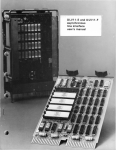
Insert the BC80M controller cable (or equivalent) into J 1 on the M806I as shown in Figure
3-4.
6.
Insert the M806I in the selected slot in the LSI-II bus.
7
Att(lch the ground strap on the cable to the metal cabinet chassis.
8.
Connect the other end of the BC80M cable to the back of the first disk drive.
9.
Continue with the disk installation. Refer to the RLOI/RL02 Disk Subsystem User's Guide
(EK-RLOI2-UG).
"T.
3.9 ACCEPTANCE TESTING
The RLVI2 controller is tested by running the RLVI2 diskless diagnostic test and, if a drive is attached, by running the diagnostics that exercise the RLOI and RL02 disk drive. The diskless diagnostic
should be run first. The RLVI2 diagnostics are available on different media. Contact your local Digital
sales office for the types of media available and their part numbers.
Run the XXDP+ diagnostics in the following order.
1.
CVRLB RL VI2 Diskless Diagnostic (16-, 18-, or 22-bit mode)
NOTE
The RLVll diskless diagnostic (CVRLA) is compatible with the RLV12 diskless diagnostic and
checks the same logic. However, it will not check
22-bit addressing.
2.
CZRLG Controller Test Part 1
3.
CZRLH Controller Test Part 2
3-5
4.
CZRLI Drive Test Part 1
5.
CZRLJ Drive Test Part 2
6.
CZRLN Drive Test Part 3
7.
CZRLK Performance Exerciser
8.
CZRLL Compatibility Test
9.
CZRLM Bad Sector File Utility
NOTE
The Bad Sector File Utility is not a diagnostic test.
It is used by field service to examine the bad sector
file on the disk and to write entries into that file.
ATTACH TO
FIRST DISK
DRIVE
M8061
LSI-11
BACKPLANE
MR-5898
Figure 3-4
RL V12 Installation
3-6
CHAPTER 4
REGISTERS
4.1 INTRODUCTION
This chapter describes the functions of the bits in each of the five programmable registers.
NOTE
To prevent accidental writing on a disk, the RLV12
synchronizes on controller ready (CRDY). If the
CRDY bit in the CSR changes from clear to set
while the processor is in ODT mode, the next read
access of any RLV12 register produces all Os.
4.2 CONTROL/STATUS REGISTER (CSR)
The control/status register (Figure 4-1) is a I6-bit, word-addressable register with a standard address of
774400 for I8-bit addressing, and 17774400 for 22-bit addressing. Bits 1 through 9 can be read or written; the other bits can only be read. The bit functions are described in Table 4-1.
When the LSI-II bus is initialized with BINIT L, bits 1-6 and 8-13 are cleared, and bit 7 (CRDY) is
set. Bit 0 (DRDY) is set when the selected drive is ready to accept a command; otherwise, this bit is
cleared. Bit 14 (DE) is clear as long as there is no drive error. Otherwise, this bit is set and stays set
until the drive error is corrected; or if bit 3 (drive reset) is set in the DAR and the controller is sent a
Get Status command, the DE bit is cleared.
At the beginning of each controller command, error bits 10-13 are automatically cleared. At the completion of each controller command, bit 7 is automatically set. (Bit 7 is also set if an error is detected
during command execution.)
4.3 BUS ADDRESS REGISTER (BAR)
The bus address register (Figure 4-2) is a 16-bit, word-addressable register with a standard address of
774402 for I8-bit addressing, and 17774400 for 22-bit addressing. Bits 0 through 15 can be read or
written; bit 0 is usually written as O. The bus address register indicates the memory location for the
DMA data transfer during a read or write operation. The register's contents are automatically incremented by 2 as each word is transferred between the system memory and the controller.
The bus address can be expanded for an 18-bit LSI-II bus by using bits 4 and 5 (BA 16 and 17) of the
CSR or by using bits 0 and 1 of the BAE register.
The bus address can be expanded for a 22-bit LSI-II bus by using the BAE register (BAE 16-21).
NOTE
When using 22-bit mode, writing CSR bits 4 and 5
modifies BAE bits 0 and 1 and vice versa.
The BAR is cleared by initializing the bus (BINIT L).
4-1
Table 4-1
CSR Word Format
Bit(s)
Name
Description
o
DRDY
Drive Ready - When set, this bit indicates that the selected drive is ready to receive a command or supply
valid read data. The bit is cleared when a Seek or head select operation is started and set when the Seek
operation is completed.
1-3
FO-F2
Function Code - These bits are the function code set by software to indicate the command to be executed.
Function
F2
Fl
0
0
0
0
I
I
I
0
0
I
0
0
I
1
1
1
FO
0
I
0
1
0
1
0
I
Octal
Code
Command
Maintenance mode
Write Check
Get Status
Seek
Read Header
Write Data
Read Data
Read Data Without
Header Check
0
I
2
3
4
5
6
7
Command execution starts when CRDY (bit 7) of the CSR is cleared by software. The commands are
described in more detail in Chapter 5. The function code is cleared by initializing the bus (BINIT L).
4,5
BAI6,
BAI7
Extended Address Bits - These two bits are the upper-order bus address bits for 18-bit buses. These bits
are read and written as bits 4 and 5 of the CSR. They function as address bits 16 and 17 of the BAR.
Writing bits 4 and 5 of the CSR also writes bits 0 and I of the BAE.
6
IE
Interrupt Enable - When CRDY is asserted, bit 6 allows the controller to interrupt the processor. This
interrupt occurs at the termination of a command. Once an interrupt request is placed on the LS I-II bus,
it is not removed until acknowledged by the LSI-II processor even if IE (bit 6) is cleared. This bit is
cleared by initializing the bus.
7
CRDY
Controller Ready - When cleared by software, this bit indicates that the command in bits 1-3 is to be
executed. This bit is set by the controller at the completion of a command, at the detection of an error, or
by initializing the bus. Software cannot set this bit because no registers are accessible while CRDY is o.
8,9
DSO,
DS)
Drive Select - These bits determine which drive will communicate with the controller via the drive bus.
These bits are cleared by initializing the bus.
10-13
EO-E3
Controller Status Errors - These bits are the error code set by the controller to indicate one of the following errors.
Error Code
E3
E2
El
EO
Error
0
0
0
0
0
I
I
0
I
I
0
0
0
0
I
0
I
0
1
0
I
Operation incomplete (OPI)
Data CRC (DCRC)
Header CRC (HCRC)
Data late (DL T)
Header not found (HNF)
Nonexistent memory (NXM)
Parity error abort (PAR ERR)
0
0
0
I
I
0
0
Octal
Code
I
2
3
4
5
10
11
Operation incomplete indicates that the current command was not completed within the OPI timeout period of 550 ms.
A data CRC error indicates that while reading the data field from the disk, an error was found.
A header CRC error indicates that while reading the header from the disk, an error was found. The CRC
check is performed on the first and second header words, although the second header word is always o.
4-2
Table 4-1
CSR Word Format (Cont)
Bit(s)
Name
Description
10-13
EO-E3
Data late indicates that the FI FO RAM was more than half full and the controller was not able to read the
next sequential sector. This error may occur during a Read Without Header Check command.
Header not found indicates that an OPI timeout occurred while the controller was searching for the correct sector to read or write. A header compare did not occur.
A nonexistent memory error indicates that during a DMA transfer the memory location addressed did not
respond with RPL Y within lOlls.
A memory parity error abort indicates that a parity error was detected while reading the system's optional
memory that has parity error checking. I f an error was detected, the current command to the RL Vi 2 is
aborted.
14
DE
Drive Error - This bit is buffered from the drive error interface line. When set, it indicates that the selected drive has flagged an error, the source of which can be determined by executing a Get Status command. DE will not set ERR (bit 15) or CRDY (bit 7) until the usual occurrence of CRDY.
15
ERR
Composite Error - When set, this bit indicates that one or more of the error bits (bits 10-14) are set.
When an error occurs, the current operation terminates and an interrupt routine is started if the interrupt
enable bit (bit 6 of the CSR) is set.
Aii error bits are cleared by initializing the bus by starting a new command, with the exception of DE and
ERR if they were caused by a drive error.
15
ERR
~~
14
13
12
11
10
09
08
07
06
05
04
03
02
01
00
D
OPI
DE NXM DLT
eRe 0
H OPI
PAR
HNF
eRe 1
ERR
_ _ _ _ _ _ _ _ _ _, ,________AA_________________, ,_ _ _ _ _ _ _ _ _ _ _ _ _~
READ ONLY
READMIRITE
READ
ONLY
MR·5751
Figure 4-1
12
BA14
11
10
Control/Status Register (CSR)
09
08
07
06
05
04
03
02
01
00
BA10
\~------------------------~,,--------------------------~)
READIWRITE
Figure 4-2
Bus Address Register (BAR)
4-3
MR 5752
4.4 DISK ADDRESS REGISTER (DAR)
The disk address register is a 16-bit, read/write, word-addressable register with a standard address of
774404 for IS-bit addressing, and 17774404 for 22-bit addressing. Its contents has one of three meanings, depending on the command being performed.
Command
DAR Function
Seek
Head selected, number of cylinders to move, direction
Read Data
or Write Data
Head selected, cylinder address, sector address
Get Status
Send drive status to MPR; reset error registers
The DAR is cleared by initializing the bus (BINIT L).
4.4.1 DAR During a Seek Command
To perform a Seek command, the program must provide the head selected (HS), direction to move
(DIR), and the cylinder address difference (OF), as indicated in Figure 4-3. The bits are described in
Table 4-2.
4.4.2 DAR During a Read, Write, or Write Check Command
For a Read, Write, or Write Check command, the DAR provides the head selected (HS) and the address of the first sector to be transferred (SA), as indicated in Figure 4-4. The bits are described in
Table 4-3. As each sector is transferred, the DAR sector address increments by 1.
4.4.3 DAR During a Get Status Command
Both the CSR and the DAR must be programmed to perform a Get Status command. The DAR must
be programmed as shown in Figure 4-5. Then a Get Status command is placed in the CSR. The DAR
bits are described in Table 4-4.
4.5 MULTIPURPOSE REGISTER (MPR)
The multipurpose register is a 16-bit, read/write, word-addressable register. It is accessed using the
standard address of 774406 for IS-bit addressing, and 17774404 for 22-bit addressing. Following a
Read Header command or a Get Status command, reading the MPR obtains sector header or drive
status information.
Writing to the MPR is used to set the word count. The word count is cleared by initializing the bus
(BINIT L).
4.5.1 Writing the MPR to Set the Word Count
Before starting a DMA transfer, the MPR is loaded with the word count. The program must load the
MPR with the 2's complement of the number of words to be transferred. The MPR is written in the
format shown in Figure 4-6. The bits are described in Table 4-5. As each word is transferred, the MPR
is automatically incremented by 1. The reading or writing operation continues until a word count overflow occurs, indicating that all words have been transferred.
The word count can range from I to 5120 data words. The maximum word count is limited by the
maximum number of sectors available (40) and the maximum words per sector (12S).
NOTE
Once written the word count cannot be read back.
Reading the l\IPR does not change the word count.
4-4
15
14
13
12
11
10
09
08
07
06
05
04
03
00
(RL02 ONLY)
MR5753
Figure 4-3
Table 4-2
DAR During a Seek Command
DAR Seek Command Word Format
Bit(s)
Name
Description
o
MRKR
Marker - Must be a I.
none
Must be a 0, indicating to the drive that a Seek command is being issued and that the other bits in the
register hold the Seek specifications.
2
DIR
Direction - This bit indicates the direction in which the Seek is to take place. When the bit is set, the
heads move toward the spindle (to a higher cylinder address). When the bit is cleared, the heads move
away from the spindle (to a lower cylinder address). The actual distance moved depends on the cylinder
address difference (bits 7-15).
3
none
Must be a O.
4
HS
Head Select - Indicates which head (disk surface) is to be selected: 1
5, 6
none
Reserved
7-15
DF
Cylinder Address Difference - I ndicates the number of cylinders the heads are to move on a Seek.
14
13
12
11
10
09
08
=
lower, 0
=
upper.
07
MR·5754
Figure 4-4
DAR During a Read, Write, or Write Check Command
Table 4-3
DAR Read/Write Data Command Word Format
Bit(s)
Name
Description
o5
SA
Sector Address - Address of one of the 40 sectors on a track. (Octal range is 0 to 47.)
6
HS
Head Select - Indicates which head (disk surface) is to be selected: I = lower: 0 = upper.
7-15
CA
Cylinder Address - Address of one of the 156 cylinders for RLOI or 512 cylinders for RL01. (Octal range
is 0 to 777.)
4-5
15
14
13
12
11
10
09
08
I I I I I I I I
x
x
x
x
x
x
x
07
06
0
0
x
05
I
0
04
0
03
02
01
00
I I I I I
RST
0
1
1
MR-5755
Figure 4-5
Table 4-4
DAR During a Get Status Command
DAR Get Status Command Word Format
Bit(s)
Name
Description
o
MRKR
Marker - Must be a 1.
GS
Get Status - Must be aI, indicating to the drive to send its status word. At the completion of the Get
Status command, the drive status word is read into the controller multipurpose register (MPR). With this
bit set, bits 8-15 are ignored by the drive.
2
none
Must be a O.
3
RST
Reset - When this bit is set, the disk drive clears its error register of soft errors before sending a status
word to the controller.
4-7
none
Must be a O.
8-15
none
Not used.
15
14
13
12
11
10
09
08
07
06
05
04
03
02
01
00
we11
Figure 4-6
Writing the MPR to Set the Word Count
Table 4-5
MPR Word Count Format
Bits
Name
Description
0-12
WC
Word Count - This is the 2's complement of the total number of words to be transferrcd.
13-15
none
Must be allIs for word count in correct rangc.
4-6
4.5.2 Reading the MPR After a Read Header Command
When a Read Header command is executed, three words can be sequentiaily read from the MPR, as
shown in Figure 4-7. The first word includes the sector address, the head selected, and the cylinder
address. The second word is al! Os. The third word has the header CRC information.
4.5.3 Reading the MPR After a Get Status Command
After a Get Status command is executed, a status word is stored in the NfPR, as shown in Figure 4-8.
The status word from the selected disk drive includes information on the functional state of the drive
and any drive errors. The bits are described in Table 4-6.
4.6 BUS ADDRESS EXTENSION REGISTER (BAE)
The bus address extension register is a 6-bit read/write register used to drive address bits 16-21 for a
22-bit LSI-II bus. The BAE has a standard address of 17774410 for 22-bit addressing. A write to the
BAE loads TS DAL 0-5 into BAE 0-5, shown in Figure 4-9. Reading the BAE enables bank select 7
(BBS7 L) to the LSI-II bus. (A jumper must be connected between M 1 and M2 on the controller to
enable 22-bit addressing; see Chapter 3.) When address bits 13-21 are allIs, the RLV12 drives BBS7
L to direct data to the I/O page.
The two least significant bits of the BAE (bus address lines 16 and 17) are mirrored in bits 4 and 5 of
the CSR. The same bits can be read or written as CSR bits 4 and 5 or BAE bits 0 and 1.
NOTE
Writing CSR bits 4 and 5 modifies BAE bits 0 and 1
and vice versa.
The BAE register is cleared by initializing the bus (BIN IT L).
15
~~~DI
a
14
I
a
13
I
12
a
a
I
11
I
a
10
I
a
09
I
a
08
I
a
07
I
a
06
I
a
05
I
a
04
I
03
a
I
a
02
I
a
01
I
a
00
I
a
I
3RD
WORD
CRC8
CRC14
CRC6
CRC4
MR-5757
Figure 4-7
15
14
13
Reading the MPR After a Read Header Command
(Three Header Words)
12
11
10
09
08
SKTO
07
06
05
04
03
02
01
00
STATE
MR·5758
Figure 4-8
Reading the MPR After a Get Status Command
4-7
Table 4-6
MPR Status Word Format
Bit(s)
Name
Description
0-2
ST A,
STB,
STC
These bits (A, B, and C) define the state of the drive as follows.
C
B
A
State of Drive
0
0
0
0
0
0
0
1
1
1
1
1
1
0
0
0
1
0
Load state
Spin up
Brush cycle
Load heads
Seek track counting
Seek linear mode (lock on)
Unload heads
Spin down
1
1
1
1
0
1
3
BH
Brush Home - Asserted when the brushes are not over the disk.
4
HO
Heads Out - Asserted when the heads are over the disk
5
CO
Cover Open - Asserted when the cover is open or the dust cover is not in place.
6
HS
Head Select - Indicates the head selected: I = lower, 0 = upper.
7
DT
Drive Type - Indicates the type of disk drive: 0 = RLO I, 1 = RL02.
8
DSE
Drive Select Error - Indicates multiple drive selection is detected.
9
VC
Volume Check - VC is set every time the drive goes into load heads state. This asserts a drive error at the
controller, but not on the front panel. VC is an indication that the program does not know which disk is
present until it has read the serial number and bad sector file. (The disk might have been changed while
the heads were unloaded.)
10
WGE
Write Gate Error - Indicates that the write gate was asserted when the drive was not ready, the sector
pulse was asserted, or the drive was write-locked.
II
SPE
Spin Error - Indicates that the spindle did not reach full speed within a specific time, or it is turning too
fast.
12
SKTO
Seek Time Out - Indicates the heads did not come onto track within a specific time during a Seek command.
13
WL
Write Lock - Indicates write lock status of selected drive: 0 = unlocked; I = protected.
14
HCE
Head Current Error
15
WDE
Write Data Error - Indicates write gate was asserted, but no pulses were detected on the write data line.
15
a
14
13
I ndicates write current was detected in the heads when write gate was not asserted.
12
11
10
Ia I a I a I a Ia
09
08
07
06
a[a
05
[I
I
BA21
Figure 4-9
04
sJ20
03
I
I
BA19
BAE Register Word Format
4-8
02
S118
01
00
I I
I Bd16
BA17
CHAPTER 5
COMMANDS
5.1 INTRODUCTION
This chapter describes the commands that are sent to the control/status register, FO, F 1, F2, to perform
a specific disk function. The number in parentheses after each command is the octal code for the command.
A prerequisite to issuing any command is that CRDY (controller ready) is set in the CSR (bit 7). Software cannot set this bit and cannot access any register if this bit is O.
At the start of each new command, the error bits in the CSR (bits 10-13) are automatically cleared. At
the completion of each command, the CRDY bit is automatically set. (CRDY is also set if an error is
detected during command execution.)
5.2 WRITE CHECK (1)
Prerequisite: The disk heads must be placed at the correct track by issuing a Seek command if necessary. The BAR must be loaded with the address of the first location of the data block in system memory. The word count of the data block length must be loaded in the MPR. The DAR must be loaded with
the starting disk address location.
The Write Check command is used to verify that data was written on the disk correctly. It is used after
writing a block of data on the disk by the Write Data command.
The Write Check cO!D!DaDd reads this same block of n8t8 8nn c()mr~res it with the d~t~ in the computer's system memory. Because this comparison is performed in the controller, this source data must
be transferred out of memory into the controller's FI Fa buffer. A bit-by-bit comparison of the header
on the disk and the contents of the disk address register checks for a header match.
Once a header match is found and the header CRC validates the match. the 128 words of data are read
from the disk. This data is then compared with the serial data coming out of the FI Fa serializer (SER
DATA OUT). A compare error or a data CRC error sets bit 1 1 in the CSR.
NOTE
When writing only a partial sector (less than 128
words), words with all Os are used to fill the remaining portion of the sector.
5.3 GET STATUS (2)
Prerequisite: The software should first verify that the controller ready bit is set. (The drive does not
have to be ready.) Then a status request word must be loaded into the DAR. Bits 0 and 1 must be set;
bit 3 (reset) can be either 0 or 1; and all other bits must be Os. (See Paragraph 4.4.3.)
A Get Status command in the CSR asks the selected disk drive to return information about its current
operation and error status. If the reset bit (bit 3) is set in the DAR, the disk drive first clears its error
register of all soft errors before sending back the drive status. When the drive sends back its status
word, it is stored in the FIFO buffer and can be accessed by reading the MPR.
5-1
DRDY (drive ready) does not have to be set to issue a Get Status command. For example, a Get Status
command can be issued during a seek operation or when the drive is in its load state.
5.4 SEEK (3)
Prerequisite: The present location of the disk head must be known. This can be determined with a Read
Header command. Then the software must compute the cylinder address difference (DF) needed by the
drive to move the heads to the new location. Then the DAR must be loaded with the head positioning
information. The DAR must include the number of cylinders to move (bits 7-15), the head select bit
(bit 4), and the direction to move (bit 2). Bits 6, 5, and 1 must be set to 0; bit 0 must be set to 1.
The Seek command shifts the contents of the DAR to the disk drive. The DAR contains the head selected for the next data transaction, the cylinder difference address, and the direction of movement.
Once the drive receives this head positioning information, it moves the head to the new track location.
5.5 READ HEADER (4)
Prerequisite: A Get Status command must be issued and DRDY must be set in the CSR.
The Read Header command reads the first header found on the selected drive and stores the three
header words in the FI FO RAM. The first word, WD 1, includes the cylinder address, the head selected, and the sector address. The second word, WD2, is all zeros. The third word, WD3, has the header CRC information. These words can be read from the FIFO RAM buffer by consecutive read MPR
instructions. Three read MPR instructions are needed to read three FIFO words. Reading the first
header word provides enough head positioning information to permit software computation of the cylinder difference for another Seek command to a new track address.
5.6 WRITE DATA (5)
Prerequisite: The head must be loaded at the correct track, by issuing a Seek command if necessary.
The 2's complement of the words to be written (word count) must be loaded into the MPR.
The Write Data command enables the controller DMA circuitry. The RL V 12 becomes LSI-II bus
master, and data words are loaded into the FIFO buffer. When the drive is ready, header information is
read from the disk and compared with the first sector address stored in the DAR. Once a header match
is found, the FI FO data is written on the disk in sequential sectors until the word count is complete. The
BAR and word count are incremented for each word transferred. If only part of a sector is filled by the
new data, the rest of the sector area is filled with Os. At the end of the sector, the sector part of the
DAR is incremented. At the end of a transfer, CRDY is set and an interrupt is made if IE is set.
5.7 READ DATA (6)
Prerequisite: The head must be loaded at the correct track, by issuing a Seek command if necessary.
The 2's complement of the words to be read (word count) must be loaded into the MPR.
The Read Data command causes headers to be read from the disk and compared to the sector address
stored in the DAR. When a header match is found, disk data words are transferred into the FI FO memory. Both the BAR and word count are incremented for each word transferred. After four words are
read from the disk, the microsequencer starts a DMA transfer on the LSI-II bus. The data transfer
ends when the word counter overflows. I f the word count is not complete, the next sector is read. Otherwise, CRDY is set and an interrupt is made if IE is set.
5.8 READ WITHOUT HEADER CHECK (7)
Prerequisite: The location of the sector with the bad header must be known. The BAR must be loaded
with the starting memory location to place the words to be read. The MPR must be loaded with the
word count in 2's complement form.
5-2
The Read Without Header Check allows the recovery of data if the headers cannot be read. If header
not found (HNF) or header CRC (HCRC) errors are found on a sector, then data cannot be recovered
by the usual Read Data command.
A Seek command must be issued to position the head on the sector with the bad header. Then the sector
preceding the bad sector must be found by performing consecutive Read Header commands. Finally a
Read Without Header Check command must be issued within 300 }.LS to recover the data in the bad
sector. The BAR and word count are incremented for each word transferred. Data CRC is checked at
the end of a sector. If the word count is not complete, the next sector is read. Otherwise, CRDY is set
and an interrupt is made if IE is set.
NOTE
The DAR is automatically incremented after each
sector is transferred.
5.9
MAINTENANCE FUNCTION (0)
Prerequisite: The BAR must be set to the first location of a test data buffer. The word count register
must be set to transfer 511 words (1177018). Too large or too small a WC results in a HNF error. (To
be compatible with RL V 11 software, a WC of 510 should not be used.)
The maintenance function allows the RL V 12 to perform a self-test operation. This function is used to
test the controller and may be executed with or without a disk drive attached. The maintenance function performs six internal tests as follows. The DAR is incremented after completion of each test.
Test
Function
1 and 2
Check internal logic
Checks DMA transfers
Checks the CRC of (DAR + 3)
Checks the CRC of (DAR + 4)
Checks the eRe of (CRC of DAR
3
4
5
6
+
4)
CAUTION
Memory locations are modified by this function.
Under DMA control, 256 words are transferred from memory, beginning at the starting address in the
BAR through BAR + 7768, to the FI FO RAM. Then all but the last word is transferred back into the
next 255 memory locations, starting at BAR + 10008 through BAR + 17748.
Next, the contents of the DAR are used to test the serial read/write data paths. The data uses an internal loop and is not transmitted to the disk drive. The CRC of the DAR + 3 and the CRC of the (CRC
of DAR + 4) are stored in the FIFO RAM and can be read by reading the MPR. The DAR's low byte
(bits 0-7) holds its original contents + 6.
The DAR's high byte (bits 8-15) is not incremented even when an overflow occurs out of the low byte.
5.10 EXAMPLES OF USING COMMANDS
Paragraphs 5.10.1 and 5.10.2 provide examples of the use of RL V 12 commands in software programs.
5-3
5.10.1 Seek Operation
The following example illustrates the sequence of events for programming a seek operation.
1.
Issue a Read Header command to the desired disk drive and wait for an interrupt request or
wait for CRDY.
2.
Check error flag in the CSR.
3.
Read the header word from the MPR.
4.
Compute the difference address and the direction for the seek.
5.
Write the difference word into the DAR.
6.
Issue the Seek command to the drive and wait for seek to be completed as indicated by
DRDY.
7.
Check error flag in the CSR.
Steps 1, 2 and 3 above are not needed for the next Seek commands if the software program keeps the
current cylinder address and head selected in memory.
Reading sequential headers gives head position and present direction so the program can optimize the
shortest distance to the new location.
5.10.2 Data Transfer Operation
The following example illustrates the sequence of events for programming a data transfer (read or
write) operation.
I.
Perform the steps of the seek operation previously described.
2.
Write the bus address in the BAR.
3.
Write the extended bus address in the BAE if using 22-bit addressing.
4.
Write the DAR with the cylinder address, head selected, and sector address of the first disk
location to be transferred.
5.
Load the MPR with the word count (2's complement of words to be transferred).
6.
Issue a Read Data, Write Data, or Write Check command in the CSR.
7.
Wait for interrupt or test for CRDY.
8.
Check the CSR for an error flag.
Seek commands or data transfer commands may be given to other drives between issuing a Seek to the
first drive and issuing a data transfer command.
As soon as a Seek command is issued to the first drive, it returns an interrupt and sets CRDY. A Seek
command may be given to another drive while the first drive is seeking. No interrupts occur when all
the seeks are complete, so as soon as all Seek commands are issued, data transfer commands may be
issued. Starting with the drive that was given the shortest seek distance makes it possible for the drive
that completes its seek first to immediately perform its data transfer and interrupts when done.
5-4
5.11 ERROR RECOVERY
Errors can be detected and flagged in the RL V 12 and RLO 1/RL02 subsystem. Some of the errors can
be recovered~ that is, if the operation is tried again, the error may not occur again. Some of the errors
are fatal and could result in loss of the data, or damage to the media or equipment. The errors are listed
with the recommended action in Table 5-1. The following examples suggest the kinds of questions to
consider when programming error recovery routines.
The type of error is a factor in determining how many times to retry the operation. For example, a data
late (DL T) error could be caused by a hardware system failure, but it could also be the result of bus
activity by other I/O devices exceeding their throughput capability for a short duration. In the later
case, the operation could be successful on the first retry.
The rate of error occurrence is a good indicator of system performance. An error logging routine should
be used to obtain this information. If the rate of DL T errors increases, it could indicate hardware system failures, or it could indicate that the system is reaching its throughput capacity in its present configuration.
Another example of applying practical consideration to an error is with a header not found (HN F) error. After a retry, if the error occurs again, then possibly the head is not positioned over the correct
track. if a read header operation is performed and the address for the media is examined, the current
cylinder and head can be determined to see if it is a position problem. If it is not, then possibly there is a
bad spot on the media and another area should be tried. If there is a bad header, that sector address
should be entered into the Bad Sector File on the disk and the software should not use this bad sector.
Error log files should be maintained and consulted to help determine error causes. When an error occurs, the program should log it with facts such as the contents of the registers, the status of the unit, and
whether or not a retry was successful. The more compiete the error iog, the faster the cause can be
diagnosed.
5-5
Table 5-1
Controller Status Errors
Controller
Error
CSR
Bit(s)
Recommended Action
OPI
10
Operation incomplete; retry a limited number of times.
DCRCjHCRC
11
Data or header CRC error; retry a limited number of times. Record the contents of the
DAR.
DLT
12
Data late; retry.
HNF
10, 12
Header not found; perform a Read Header command and verify cylinder.
NXM
13
Nonexistent memory; retry once. Record the contents of the BAR.
Parity Error
Abort
10, 13
The command to the controller is aborted; retry.
Drive Error
14
Perform a Get Status command and check MPR for disk drive status errors; see Table 5-2.
Table 5-2
Disk Drive Status Errors
Orive
Error
MPR Drive
Status Bit
Recommended Action
CO
5
Cover open; close cover.
DSE
8
Multiple drive selection is detected. Retry once before telling operator to verify unit select plug.
WGE
10
Write gate error: retry. Drive is not ready. drive is write protected. or drive has another error.
SPE
II
Spin error; retry.
SKTO
12
Seek time out; reset drive and wait for 1.5 second before sending another Seek command.
WL
13
Write lock; drive is write protected.
CHE
14
Current head error. This error is fatal; do not retry. Write current is detected in the heads.
WDE
15
Write data error. This error is fatal; do not retry. No transitions are detected.
5-6
CH~t\PT1{.R
6
DISK DRIVE
6.1
INTRODUCTION
The RL V 12-AK and the RL V22-AK come complete with an RLO 1 or RL02 disk drive, respectively.
The following switches and indicators are found on the front of the disk drive (see Figure 6-1).
Run/Stop switch with LOAD indicator
Unit Select plug with READY indicator
FAULT indicator
WRITE PROTECT switch and indicator
Power ON/OFF control is a circuit breaker switch on the back of the disk drive. Operation of this
switch will not damage the drive; however, this switch is usually left ON.
The user can select the voltage and range for each disk drive on the back of the drive.
LOAD
(RUN/STOP)
READY
(UNIT SELECT)
FAULT
WRITE
PROT
MR-1860
Figure 6-1
RLOI/RL02 Disk Drive (Front View)
6-1
6.2 USER SWITCHES AND INDICATORS
This paragraph provides information on each switch and indicator.
Run/Stop Switch with LOAD Indicator - The run/stop switch when pressed, energizes the spindle motor. When pressed again, the switch turns off the spindle motor as long as the heads and brushes are
home. If the heads are loaded, pressing the switch causes the heads to unload and then turns off the
spindle motor.
The switch has a mechanical memory. If the spindle motor is energized and the main power is lost for a
short time, the spindle motor energizes again.
The LOAD indicator is on when the spindle is stopped, head is home, brushes are home, and the spindle
motor is not energized. A cartridge can be loaded when this indicator is lit.
Unit Select Plug with READY Indicator - The unit select plug is a cam button that is inserted in a
switch. The switch contacts are binary encoded for the unit select number (0, 1, 2, or 3) on the cam
button. The READY indicator lights to indicate a drive ready condition; that is, the heads are loaded
on a cylinder ready for a read or a write operation.
FAULT Indicator - The F AUL T indicator comes on when an error condition occurs in the drive.
WRITE PROTECT Switch and Indicator - The WRITE PROTECT switch, when pressed, sets the
drive in write protect mode. If the drive is in the process of writing at the time that the switch is
pressed, writing continues until the next sector pulse. The WRITE PROTECT indicator is on when the
write protect function is enabled. Pressing the WRITE PROTECT switch again turns off the write
protect mode and indicator.
6.3
110/220 VOLTAGE AND NORMAL/LOW VOLTAGE RANGE SETTING
The voltage selection and voltage range are each set by a terminal block cover, shown in Figure 6-2.
They should be set according to Table 6-1.
For systems operating with low line voltage, proceed as follows to change the NORMAL/LOW terminal block cover.
1.
2.
3.
4.
Remove the two screws from the NORMAL/LOW terminal block cover.
Withdraw the cover and reinsert it turned upside down.
After insertion, '"LOW" must be showing through the small window in the cover.
Replace the two screws.
For systems operation at 220 Vac, 50 or 60 Hz, proceed as follows to change the voltage selection.
1.
2.
3.
4.
Remove the two screws from the 110/220 terminal block cover.
Withdraw the cover and reinsert it upside down.
After insertion, "220" must be showing through the small window in the cover.
Replace the two screws.
6-2
I/O CABLE
/
TERMiNATOR
COVER
MR·6584
Figure 6-2
Table 6-1
RLOl/RL02 Disk Drive (Rear View)
Voltage and Range Selector Setting
Line Voltage
110/220
Setting
90-105 Vac
100-127 Vac
180-210 Vac
200-254 Vac
110
110
220
220
NORMAL/LOW
Setting
LOW
NORMAL
LOW
NORMAL
6-3
RLV12 Disk Controller User's Guide
EK-RLV12-UG-002
Reader's Comments
Your comments and suggestions will help us in our continuous effort to improve the quality and usefulness of our publications.
What is your generai reaction to this manual? In your judgement is it complete. accurate. well organized.
well written. ett? Isiteasytouse?~~~~~~~~~~~~~~~~~~~~~~~~~~~
What features are most useful? _ _ _ _~~~~~~~~~~~~~~~~~_~~~_~~~_
What faults or errors have you found in the
manual?_~~~~~~~~_ _~~_""'-_~_ _~_
Does this manual satisfy the need you think it was intended to satisfy? _ _ _ _ _~_ _ _ _ _~_ _
Does it satisfy your needs? _ _ _ _~_ _ _ __
o
Why? ______
~~~~
___________________
Please send me the current copy of the Technical Documentation Catalog. which contains information
on the remainder of DIGITAL's technical documentation.
__
_______
__
Name ____
Title _ _~_ _~~__~~~__~~~__~~~_
Company __~_~~__~~~__~_~__~~~_
Department __~~_~~~~__~_~____~___
~~
~~~
~~
Additional copies of this document are available from:
Digital Equipment Corporation
Accessories and Supplies Group
Cotton Road
Nashua. N H 03060
Attention Documentation Products
Telephone 1-800-258-1710
Order No. E K-R LV12-UG
Street ____~~_~~~_ _~_ _~~_
City ________________________________
State/COuntry _ _ _ _ _ _ _ _ _ _ _ _ __
Zip _______________________________
Fold Here
Do Not Tear - Fold Here and Staple
IIIIII
No Postage
Necessary
if Mailed in the
United States
BUSINESS REPLY MAIL
FIRST CLASS
PERMIT NO.33
MAYNARD, MA
POSTAGE WILL BE PAID BY ADDRESSEE
Digital Equipment Corporation
Educational Services Development and Publishing
200 Forest Street (MR1·2/T17)
Marlboro, MA 01752
Digital Equipment Corporation· Bedford, MA 01730