1
ST9
USER GUIDE
1 ABOUT THIS GUIDE
Welcome to the ST9 User Guide. The aim of this book is to help you to get a working knowledge of the ST9 microcontroller family. Using this foundation, you will be in a good position to
understand and implement any of the ST9 microcontrollers. To make it easier, we have selected the major technical concepts of the ST9 family and will introduce them gradually over
several chapters, always supporting theory with practical examples.
1.1 PREREQUISITES
This book addresses application developers. To fully benefit from the book content, you
should be familiar with microcontrollers and their associated development tools.
For basic information on microcontrollers and development tools, you should refer to one of
the many introductory books available on the subject.
1.2 RESULTS
The book will provide you with:
■
A basic understanding of the ST9 microcontroller family
■
Knowledge and ready-to-use examples on using ST9 peripherals
■
Useful tips and warnings
Rev. 1.5
January 2004
1/146
1
Table of Contents
1 ABOUT THIS GUIDE . . . . . . . . . . . . . . . . . . . . . . . . . . . . . . . . . . . . . . . . . . . . . . . . . . 1
1.1
1.2
1.3
1.4
1.5
1.6
PREREQUISITES . . . . . . . . . . . . . . . . . . . . . . . . . . . . . . . . . . . . . . . . . . . . . . . 1
RESULTS . . . . . . . . . . . . . . . . . . . . . . . . . . . . . . . . . . . . . . . . . . . . . . . . . . . . . . 1
HOW TO USE THIS GUIDE . . . . . . . . . . . . . . . . . . . . . . . . . . . . . . . . . . . . . . . 5
COMPANION SOFTWARE . . . . . . . . . . . . . . . . . . . . . . . . . . . . . . . . . . . . . . . . 5
ABOUT THE AUTHORS . . . . . . . . . . . . . . . . . . . . . . . . . . . . . . . . . . . . . . . . . . 5
RELATED DOCUMENTS . . . . . . . . . . . . . . . . . . . . . . . . . . . . . . . . . . . . . . . . . 6
2 INTRODUCING THE ST9 BASICS . . . . . . . . . . . . . . . . . . . . . . . . . . . . . . . . . . . . . . . . 7
2.1
2.2
PROCESSOR CORE . . . . . . . . . . . . . . . . . . . . . . . . . . . . . . . . . . . . . . . . . . . . . 7
PERIPHERALS . . . . . . . . . . . . . . . . . . . . . . . . . . . . . . . . . . . . . . . . . . . . . . . . . 8
2.2.1 ST92F124 . . . . . . . . . . . . . . . . . . . . . . . . . . . . . . . . . . . . . . . . . . . . . . . . . 9
2.2.2 ST92F150 . . . . . . . . . . . . . . . . . . . . . . . . . . . . . . . . . . . . . . . . . . . . . . . . 11
2.2.3 ST92F250 . . . . . . . . . . . . . . . . . . . . . . . . . . . . . . . . . . . . . . . . . . . . . . . . 13
3 PROCESSOR CORE: MAIN CONCEPTS . . . . . . . . . . . . . . . . . . . . . . . . . . . . . . . . . 14
3.1
3.2
3.3
3.4
3.5
3.6
ADDRESS SPACES . . . . . . . . . . . . . . . . . . . . . . . . . . . . . . . . . . . . . . . . . . . . 14
3.1.1 Register-Oriented Programming Model . . . . . . . . . . . . . . . . . . . . . . . . . . 14
3.1.2 Register File . . . . . . . . . . . . . . . . . . . . . . . . . . . . . . . . . . . . . . . . . . . . . . 15
3.1.3 Direct access to the Register File . . . . . . . . . . . . . . . . . . . . . . . . . . . . . . 15
3.1.4 Working Registers . . . . . . . . . . . . . . . . . . . . . . . . . . . . . . . . . . . . . . . . . . 16
3.1.5 Peripheral Register Pages . . . . . . . . . . . . . . . . . . . . . . . . . . . . . . . . . . . . 16
3.1.6 Working Registers and Register Pointers . . . . . . . . . . . . . . . . . . . . . . . . 16
3.1.7 Memory Management Unit . . . . . . . . . . . . . . . . . . . . . . . . . . . . . . . . . . . 22
STACK MODES . . . . . . . . . . . . . . . . . . . . . . . . . . . . . . . . . . . . . . . . . . . . . . . . 31
INSTRUCTION SET . . . . . . . . . . . . . . . . . . . . . . . . . . . . . . . . . . . . . . . . . . . . . 32
3.3.1 Overview . . . . . . . . . . . . . . . . . . . . . . . . . . . . . . . . . . . . . . . . . . . . . . . . . 33
3.3.2 Advantages when Using C Language . . . . . . . . . . . . . . . . . . . . . . . . . . . 40
INTERRUPTS . . . . . . . . . . . . . . . . . . . . . . . . . . . . . . . . . . . . . . . . . . . . . . . . . 41
3.4.1 Interrupt Vectors . . . . . . . . . . . . . . . . . . . . . . . . . . . . . . . . . . . . . . . . . . . 42
3.4.2 Interrupt Priorities . . . . . . . . . . . . . . . . . . . . . . . . . . . . . . . . . . . . . . . . . . 47
3.4.3 External Interrupt Unit . . . . . . . . . . . . . . . . . . . . . . . . . . . . . . . . . . . . . . . 51
DMA CONTROLLER . . . . . . . . . . . . . . . . . . . . . . . . . . . . . . . . . . . . . . . . . . . . 56
3.5.1 Overview . . . . . . . . . . . . . . . . . . . . . . . . . . . . . . . . . . . . . . . . . . . . . . . . . 56
3.5.2 How the DMA Works . . . . . . . . . . . . . . . . . . . . . . . . . . . . . . . . . . . . . . . . 57
RESET AND CLOCK CONTROL UNIT (RCCU) . . . . . . . . . . . . . . . . . . . . . . . 60
3.6.1 Clock Control Unit . . . . . . . . . . . . . . . . . . . . . . . . . . . . . . . . . . . . . . . . . . 60
3.6.2 Reset and Stop Manager . . . . . . . . . . . . . . . . . . . . . . . . . . . . . . . . . . . . . 64
4 USING THE ON-CHIP PERIPHERALS . . . . . . . . . . . . . . . . . . . . . . . . . . . . . . . . . . . 65
4.1
4.2
2/146
1
146
PROGRAMMING THE CORE AND PERIPHERALS . . . . . . . . . . . . . . . . . . . . 65
PARALLEL I/O . . . . . . . . . . . . . . . . . . . . . . . . . . . . . . . . . . . . . . . . . . . . . . . . . 66
Table of Contents
4.3
4.4
4.5
4.6
4.7
4.8
STANDARD AND WATCHDOG TIMERS . . . . . . . . . . . . . . . . . . . . . . . . . . . . 68
4.3.1 Description . . . . . . . . . . . . . . . . . . . . . . . . . . . . . . . . . . . . . . . . . . . . . . . . 68
4.3.2 Timer Application for Periodic Interrupts . . . . . . . . . . . . . . . . . . . . . . . . . 72
4.3.3 Watchdog Application 1: Generating a PWM . . . . . . . . . . . . . . . . . . . . . 73
4.3.4 Watchdog Application 2: Using the Watchdog . . . . . . . . . . . . . . . . . . . . 74
MULTIFUNCTION TIMER . . . . . . . . . . . . . . . . . . . . . . . . . . . . . . . . . . . . . . . . 75
4.4.1 Generating Two Pulse Width Modulated Waves with One MFT . . . . . . . 79
4.4.2 Generating a Pulse Width Modulated Wave with a Cleaner Spectrum . . 82
4.4.3 Incremental Encoder Counter . . . . . . . . . . . . . . . . . . . . . . . . . . . . . . . . . 84
4.4.4 MFT Application 1: Generating 2 PWMs using Interrupts . . . . . . . . . . . . 86
4.4.5 MFT Application 2: Generating a PWM using DMA . . . . . . . . . . . . . . . . 86
4.4.6 MFT Application 3: Generating a PWM using the DMA Swap Mode . . . 87
SERIAL PERIPHERAL INTERFACE . . . . . . . . . . . . . . . . . . . . . . . . . . . . . . . . 88
4.5.1 Description . . . . . . . . . . . . . . . . . . . . . . . . . . . . . . . . . . . . . . . . . . . . . . . . 88
4.5.2 Static Liquid-Crystal Display Interface Example . . . . . . . . . . . . . . . . . . . 88
4.5.3 EEPROM Serial Interface Example using I²C . . . . . . . . . . . . . . . . . . . . . 91
SERIAL COMMUNICATIONS INTERFACE . . . . . . . . . . . . . . . . . . . . . . . . . . 92
4.6.1 Description . . . . . . . . . . . . . . . . . . . . . . . . . . . . . . . . . . . . . . . . . . . . . . . . 92
4.6.2 SCI Application 1: Sending Bytes using Interrupts . . . . . . . . . . . . . . . . . 97
4.6.3 SCI Application 2: Sending Bytes using DMA . . . . . . . . . . . . . . . . . . . . . 97
4.6.4 SCI Application 3: Sending and Receiving Bytes using DMA . . . . . . . . . 97
4.6.5 SCI Application 4: Matching Input Bytes . . . . . . . . . . . . . . . . . . . . . . . . . 97
ANALOG TO DIGITAL CONVERTER . . . . . . . . . . . . . . . . . . . . . . . . . . . . . . . 98
4.7.1 Description . . . . . . . . . . . . . . . . . . . . . . . . . . . . . . . . . . . . . . . . . . . . . . . . 98
4.7.2 Analog Watchdog . . . . . . . . . . . . . . . . . . . . . . . . . . . . . . . . . . . . . . . . . 100
4.7.3 Interrupt Vectoring . . . . . . . . . . . . . . . . . . . . . . . . . . . . . . . . . . . . . . . . . 100
4.7.4 ADC Application: A/D Conversions and Analog Watchdog using Interrupts
101
PERIPHERAL INITIALIZATION . . . . . . . . . . . . . . . . . . . . . . . . . . . . . . . . . . . 102
4.8.1 initialization Header File . . . . . . . . . . . . . . . . . . . . . . . . . . . . . . . . . . . . 102
4.8.2 Peripheral Function File . . . . . . . . . . . . . . . . . . . . . . . . . . . . . . . . . . . . . 103
5 USING THE DEVELOPMENT TOOLS . . . . . . . . . . . . . . . . . . . . . . . . . . . . . . . . . . . 112
5.1
5.2
5.3
5.4
DEVELOPING IN C LANGUAGE . . . . . . . . . . . . . . . . . . . . . . . . . . . . . . . . . . 112
AVAILABLE TOOLS . . . . . . . . . . . . . . . . . . . . . . . . . . . . . . . . . . . . . . . . . . . . 112
INTRODUCING THE DEVELOPMENT TOOLS . . . . . . . . . . . . . . . . . . . . . . 113
PROGRAM CONFIGURATION AND INITIALISATION . . . . . . . . . . . . . . . . . 113
5.4.1 Writing the Makefile . . . . . . . . . . . . . . . . . . . . . . . . . . . . . . . . . . . . . . . . 114
5.4.2 Writing the Linker Command File using a Script File . . . . . . . . . . . . . . . 119
5.4.3 Writing the Start-Up File . . . . . . . . . . . . . . . . . . . . . . . . . . . . . . . . . . . . 121
5.5 GLOBAL INITIALISATION: CORE AND PERIPHERALS . . . . . . . . . . . . . . . 129
5.5.1 Core Initialisation . . . . . . . . . . . . . . . . . . . . . . . . . . . . . . . . . . . . . . . . . . 129
5.5.2 Peripheral Initialisation . . . . . . . . . . . . . . . . . . . . . . . . . . . . . . . . . . . . . 129
3/146
1
Table of Contents
5.5.3 Port Initialisation . . . . . . . . . . . . . . . . . . . . . . . . . . . . . . . . . . . . . . . . . . 130
5.5.4 Final Initialisation . . . . . . . . . . . . . . . . . . . . . . . . . . . . . . . . . . . . . . . . . . 130
5.6 INTERRUPT CONSIDERATIONS . . . . . . . . . . . . . . . . . . . . . . . . . . . . . . . . . 130
6 DETAILED BLOCK DIAGRAMS . . . . . . . . . . . . . . . . . . . . . . . . . . . . . . . . . . . . . . . 131
6.7
6.8
6.9
6.10
6.11
EXTERNAL INTERRUPT CONTROLLER . . . . . . . . . . . . . . . . . . . . . . . . . . . 131
TOP-LEVEL INTERRUPT INPUT . . . . . . . . . . . . . . . . . . . . . . . . . . . . . . . . . 132
WATCHDOG TIMER . . . . . . . . . . . . . . . . . . . . . . . . . . . . . . . . . . . . . . . . . . . 133
MULTIFUNCTION TIMER . . . . . . . . . . . . . . . . . . . . . . . . . . . . . . . . . . . . . . . 134
ADC . . . . . . . . . . . . . . . . . . . . . . . . . . . . . . . . . . . . . . . . . . . . . . . . . . . . . . . . 136
7 GLOSSARY . . . . . . . . . . . . . . . . . . . . . . . . . . . . . . . . . . . . . . . . . . . . . . . . . . . . . . 137
INDEX . . . . . . . . . . . . . . . . . . . . . . . . . . . . . . . . . . . . . . . . . . . . . . . . . . . . . . . . . . . . . 142
146
4/146
1
ST9 USER GUIDE
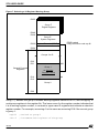
1.3 HOW TO USE THIS GUIDE
As a first approach, we recommend that you study each chapter in sequence and carry out the
exercises at each step.
1.4 COMPANION SOFTWARE
A downloadable file entitled ST9 User Guide Companion Software is available. This file provides all the source text files, listings, object files and any other files mentioned in the document.
You can download the ST9 User Guide Companion Software from the http://www.stmcu.com
website product support page. Unless otherwise specified, all the examples can be compiled
for ST92F124/ST92F150/ST92F250 by modifying the makefile and the “device.h” file, if included in the application directory.
1.5 ABOUT THE AUTHORS
This User Guide has been initially written by Jean-Luc Grégoriadès and Jean-Marc Delaplace
and revised for the ST9 by Jean-Luc Crébouw.
Jean-Luc Crébouw
A signal processing engineer, he has developed a voice synthesizer with an ST9 and conducts ST9 training programs. He acts as a field application engineer consultant for all STMicroelectronics microcontrollers.
Jean-Marc Delaplace
A former electronics design engineer, he has worked throughout his career for various U.S.
companies involved in lab automation equipment. He has used microprocessors since they
first appeared on the market and programmed microcontrollers of various brands in industrial
applications using both assembler and high-level languages.
Jean-Luc Grégoriadès
Teaches automated systems and industrial computer science at the Electrical Engineering department of the University of Cergy-Pontoise. He introduced the STMicroelectronics ST6 as a
teaching base for his microcontroller course. On this occasion, he wrote with his friend J.M
Delaplace, the book “Le ST6: Etude progressive d'un microcontrôleur” published at “Editions
DUNOD”.
5/146
1
ST9 USER GUIDE
1.6 RELATED DOCUMENTS
The following reference documents should be available for additional information:
– ST9 Datasheet
– ST9 Programming Manual
– ST9 Family GNU Software tools
– ST9 GNU C Toolchain Release note
– ST9 Family GNU C Compiler
– GNU Make Utility
You can get a current list of documentation at http://www.stmcu.com.
6/146
ST9 USER GUIDE
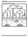
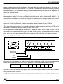
2 INTRODUCING THE ST9 BASICS
The ST9 microcontroller family has a common processor core surrounded by a range of powerful peripherals for interfacing with many different devices. The peripherals have sufficient
built-in intelligence to be able to perform even complex jobs on their own, freeing the core almost entirely from I/O handling. The core can thus be fully utilized for classical microprocessing tasks.
The ST9 architecture is an original STMicroelectronics design, with the objective of providing
an innovative and efficient microcontroller architecture dedicated to real-time control.
2.1 PROCESSOR CORE
When you compare different microcontrollers, you can estimate the relative computing power
of the core, and also of the peripherals (if they include some intelligence). In some architectures, the peripherals make heavy use of the core and thus take up a part of its computing
power. Many microcontrollers available on the market have a relatively powerful core, surrounded by very simple peripherals. This approach has the advantage of making the peripherals easy to use and configure, but at the expense of the overall computing power.
The ST9 is an example of a radically different compromise. Its core is among the best 8-bit microprocessors on the market in terms of computing performance and system management capabilities. It is assisted (rather than just surrounded) by peripheral blocks of which most can
perform complex tasks without the intervention of the core. The net result is a powerful machine that can even perform impressive tasks just using its peripherals. The three applications
described in this book give meaningful examples of processes handled solely by the peripherals.
The ST92F150 is the latest generation of the powerful ST9 microprocessor family. The new
ST9 core executes software more than three times faster than the previous ST9 core using
optimized instructions and up to double the CPU frequency. The core as well as many peripherals have been enhanced, like for example, the Memory Management Unit (MMU), which is
now more flexible, with a single 4-Mbyte memory space that is directly accessible without
using bank switching. Another example is the Reset and Clock Control Unit (RRCU) which has
added features for reducing power-consumption.
The ST9 is a register-oriented machine. This means that a large number of registers is available in the core; but above all, this implies that the instruction set is tailored to make efficient
use of its registers through optimized addressing modes. It is also well suited to the use of C
language.
7/146
ST9 USER GUIDE
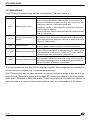
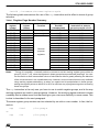
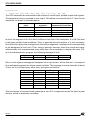
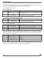
2.2 PERIPHERALS
The ST9 family includes a large number of peripherals. The main ones are:
Acronym
MFT
SCI-M
WDT
I/O port
ADC
Name
Multi-Function Timer
Function
All counting and timing functions. Includes auto-reload on condition, interrupt generation, DMA transfer, two inputs for frequency measurement or pulse counting, two outputs that can
change on condition, PWM signal generation.
Conditions include: overflow/underflow, comparison with one
or two compare registers.
Capture registers used to record transitions on inputs with their
time of occurrence.
Asynchronous transfer with either internal bit-rate generation or
Serial Communication In- an external clock. Parity generation/detection. Address recogterface
nition feature that can request an interrupt on match of an input
character. DMA transfer.
Can be used either as a watchdog or as a timer with input and
Watchdog timer
output capable of pulse counting or waveform generation.
Parallel input/output ports. Each bit individually configurable as
input, output, bi-directional, or alternate function. Inputs can be
Parallel input/output port
high impedance or with pull-up, CMOS or TTL-level. Outputs
can have open drain or push-pull configuration.
10-bit analog to digital converter. One to sixteen channels can
be converted in series. On each of two of the sixteen channels,
Analog to digital converter.
an Analog Watchdog function is used to define two thresholds.
When exceeded, an interrupt is generated.
These peripherals are available with the standard variants. More peripherals are available on
custom devices on request, e.g. a videotext decoding logic.
The ST9 family includes so many variants it would go beyond the scope of this book to describe them all. They are all made up of the same ST9 core surrounded by a set of peripherals,
ROM and/or RAM and/or EEPROM and/or FLASH being optional. This book has chosen to
show the three most generic variants and provide a basis for understanding all the others.
8/146
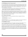
ST9 USER GUIDE
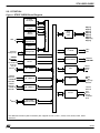
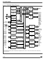
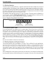
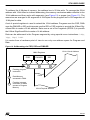
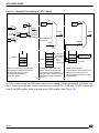
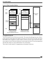
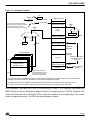
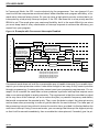
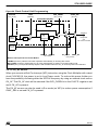
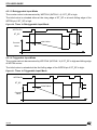
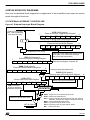
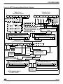
2.2.1 ST92F124
Figure 1.ST92F124R9 Block Diagram
FLASH
64 Kbytes
E3 TM
1 Kbyte
NMI
256 bytes
Register File
Fully
Prog.
I/Os
MEMORY BUS
RAM
2 Kbytes
P0[7:0]
P1[2:0]
P2[7:0]
P3[7:4]
P4[7:4]
P5[7:0]
P6[5:2,0]
P7[7:0]
8/16 bits
CPU
INT[5:0]
WKUP[13:0]
Interrupt
Management
I2C BUS
SDA
SCL
ST9 CORE
WATCHDOG
RCCU
STOUT
ST. TIMER
TINPA0
TOUTA0
TINPB0
TOUTB0
MF TIMER 0
TINPA1
TOUTA1
TINPB1
TOUTB1
MF TIMER 1
REGISTER BUS
OSCIN
OSCOUT
RESET
CLOCK2/8
INTCLK
CK_AF
SPI
ADC
SCI M
VREG
WDOUT
HW0SW1
MISO
MOSI
SCK
SS
AVDD
AVSS
AIN[15:8]
EXTRG
TXCLK
RXCLK
SIN
DCD
SOUT
CLKOUT
RTS
VOLTAGE
REGULATOR
The alternate functions (Italic characters) are mapped on Port 0, Port 1, Port2, Port3, Port4, Port5, Port6
and Port7.
9/146
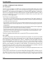
ST9 USER GUIDE
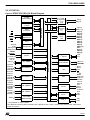
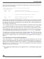
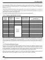
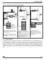
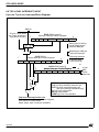
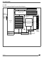
Figure 2. ST92F124V1 Block Diagram
FLASH
128 Kbytes
AS
DS
RW
WAIT
NMI
DS2
RW
INT[6:0]
WKUP[15:0]
OSCIN
OSCOUT
RESET
CLOCK2/8
INTCLK
CK_AF
RAM
4 Kbytes
256 bytes
Register File
MEMORY BUS
E3 TM
1 Kbyte
Ext. MEM.
ADDRESS
DATA
Port0
A[7:0]
D[7:0]
Ext. MEM.
ADDRESS
Ports
1,9
A[10:8]
A[21:11]
Fully
Prog.
I/Os
8/16 bits
CPU
Interrupt
Management
ST9 CORE
I2C BUS
STOUT
ST. TIMER
WATCHDOG
ICAPA0
OCMPA0
ICAPB0
OCMPB0
EXTCLK0
EF TIMER 0
ICAPA1
OCMPA1
ICAPB1
OCMPB1
EXTCLK1
EF TIMER 1
TINPA0
TOUTA0
TINPB0
TOUTB0
TINPA1
TOUTA1
TINPB1
TOUTB1
VREG
MF TIMER 0
REGISTER BUS
RCCU
SPI
ADC
SCI M
MF TIMER 1
SCI A
P0[7:0]
P1[7:3]
P1[2:0]
P2[7:0]
P3[7:4]
P3[3:1]
P4[7:4]
P4[3:0]
P5[7:0]
P6[5:2,0]
P6.1
P7[7:0]
P8[7:0]
P9[7:0]
SDA
SCL
WDOUT
HW0SW1
MISO
MOSI
SCK
SS
AVDD
AVSS
AIN[15:8]
AIN[7:0]
EXTRG
TXCLK
RXCLK
SIN
DCD
SOUT
CLKOUT
RTS
RDI
TDO
VOLTAGE
REGULATOR
The alternate functions (Italic characters) are mapped on Port 0, Port 1, Port2, Port3, Port4, Port5, Port6, Port7,
Port8 and Port9.
10/146
ST9 USER GUIDE
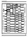
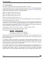
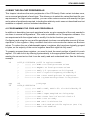
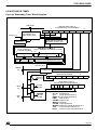
2.2.2 ST92F150
Figure 3.ST92F150C(R/V)1/9 Block Diagram
FLASH
128/64 Kbytes
INT[5:0]
INT6*
WKUP[13:0]
WKUP[15:14]*
OSCIN
OSCOUT
RESET
CLOCK2/8
INTCLK
CK_AF
STOUT
256 bytes
Register File
A[10:8]
A[21:11]*
Interrupt
Management
ST9 CORE
RCCU
I2C BUS
ST. TIMER
WATCHDOG
EF TIMER 0 *
ICAPA1
OCMPA1
ICAPB1
OCMPB1
EXTCLK1
EF TIMER 1 *
VREG
Ext. MEM.
ADDRESS
Ports
1,9*
8/16 bits
CPU
ICAPA0
OCMPA0
ICAPB0
OCMPB0
EXTCLK0
TINPA0
TOUTA0
TINPB0
TOUTB0
TINPA1
TOUTA1
TINPB1
TOUTB1
A[7:0]
D[7:0]
Fully
Prog.
I/Os
MF TIMER 0
REGISTER BUS
AS
DS
RW
WAIT
NMI
DS2
RW*
RAM
2/4 Kbytes
MEMORY BUS
E3 TM
1 Kbyte
Ext. MEM.
ADDRESS
DATA
Port0
SPI
ADC
SCI M
MF TIMER 1
SCI A*
VOLTAGE
REGULATOR
CAN_0
P0[7:0]
P1[7:3]*
P1[2:0]
P2[7:0]
P3[7:4]
P3[3:1]*
P4[7:4]
P4[3:0]*
P5[7:0]
P6[5:2,0]
P6.1*
P7[7:0]
P8[7:0]*
P9[7:0]*
SDA
SCL
WDOUT
HW0SW1
MISO
MOSI
SCK
SS
AVDD
AVSS
AIN[15:8]
AIN[7:0]*
EXTRG
TXCLK
RXCLK
SIN
DCD
SOUT
CLKOUT
RTS
RDI
TDO
RX0
TX0
* Not available on 64-pin version.
The alternate functions (Italic characters) are mapped on Port 0, Port 1, Port2, Port3, Port4, Port5, Port6, Port7,
Port8* and Port9*.
11/146
ST9 USER GUIDE
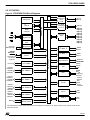
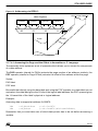
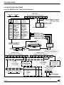
Figure 4. ST92F150JDV1 Block Diagram
FLASH
128 Kbytes
AS
DS
RW
WAIT
NMI
DS2
RW
INT[6:0]
WKUP[15:0]
E3 TM
1K byte
RAM
6 Kbytes
256 bytes
Register File
MEMORY BUS
FLASH
128 Kbytes
A[7:0]
D[7:0]
Ext. MEM.
ADDRESS
Ports 1,9
A[21:8]
Fully Prog.
I/Os
8/16 bit
CPU
J1850
JBLPD
Interrupt
Management
ST9 CORE
I2C BUS
RCCU
WATCHDOG
STOUT
ST. TIMER
ICAPA0
OCMPA0
ICAPB0
OCMPB0
EXTCLK0
EF TIMER 0
ICAPA1
OCMPA1
ICAPB1
OCMPB1
EXTCLK1
EF TIMER 1
TINPA0
TOUTA0
TINPB0
TOUTB0
MF TIMER 0
TINPA1
TOUTA1
TINPB1
TOUTB1
MF TIMER 1
VREG
VOLTAGE
REGULATOR
REGISTER BUS
OSCIN
OSCOUT
RESET
CLOCK2/8
CLOCK2
INTCLK
CK_AF
Ext. MEM.
ADDRESS
DATA
Port0
SPI
ADC
P0[7:0]
P1[7:0]
P2[7:0]
P3[7:1]
P4[7:0]
P5[7:0]
P6[5:0]
P7[7:0]
P8[7:0]
P9[7:0]
VPWI
VPWO
SDA
SCL
WDOUT
HW0SW1
MISO
MOSI
SCK
SS
AVDD
AVSS
AIN[15:0]
EXTRG
SCI M
TXCLK
RXCLK
SIN
DCD
SOUT
CLKOUT
RTS
SCI A
RDI
TDO
CAN_0
RX0
TX0
CAN_1
RX1
TX1
The alternate functions (Italic characters) are mapped on Port0, Port1, Port2, Port3, Port4, Port5, Port6, Port7,
Port8 and Port9.
12/146
ST9 USER GUIDE
2.2.3 ST92F250
Figure 5. ST92F250CV2 Block Diagram
FLASH
256 Kbytes
AS
DS
RW
WAIT
NMI
DS2
RW
INT[6:0]
WKUP[15:0]
RAM
8 Kbytes
256 bytes
Register File
MEMORY BUS
E3 TM
1K byte
Ext. MEM.
ADDRESS
DATA
Port0
A[7:0]
D[7:0]
Ext. MEM.
ADDRESS
Ports 1,9
A[21:8]
Fully Prog.
I/Os
8/16 bit
CPU
Interrupt
Management
I2C BUS _0
SDA0
SCL0
I2C BUS _1
SDA1
SCL1
ST9 CORE
STOUT
ICAPA0
OCMPA0
ICAPB0
OCMPB0
ICAPA1
OCMPA1
ICAPB1
OCMPB1
RCCU
ST. TIMER
REGISTER BUS
OSCIN
OSCOUT
RESET
CLOCK2/8
CLOCK2
INTCLK
WATCHDOG
SPI
EF TIMER 0
ADC
EF TIMER 1
SCI M
TINPA0
TOUTA0
TINPB0
TOUTB0
TINPA1
TOUTA1
TINPB1
TOUTB1
VREG
P0[7:0]
P1[7:0]
P2[7:0]
P3[7:0]
P4[7:0]
P5[7:0]
P6[7:0]
P7[7:0]
P8[7:0]
P9[7:0]
WDOUT
HW0SW1
MISO
MOSI
SCK
SS
AVDD
AVSS
AIN[15:0]
EXTRG
TXCLK
RXCLK
SIN
DCD
SOUT
CLKOUT
MF TIMER 0
SCI A
RDI
TDO
CAN_0
RX0
TX0
MF TIMER 1
VOLTAGE
REGULATOR
The alternate functions (Italic characters) are mapped on Port0, Port1, Port2, Port3, Port4, Port5, Port6, Port7,
Port8 and Port9.
13/146
ST9 USER GUIDE
3 PROCESSOR CORE: MAIN CONCEPTS
The term ST9 designates a family of components. Each component shares the same core,
surrounded by a particular configuration of memory and peripherals that make up the specific
variant. The ST9 core has a unique and powerful structure. This chapter explains the main
building blocks that you need to get familiar with to be able to make full use of its capabilities.
The main features of the core architecture are:
– Register-Oriented Programming Model
– Single-Space memory addressing
– System and User Stacks
– Interrupt system with fully integrated controller
– Built-in DMA mechanism
– Reset and Clock Control Unit (RCCU) with PLL
3.1 ADDRESS SPACES
The ST9 provides two different address spaces: Register Space and Memory Space. The
Register Space draws its power from its size: 256 registers of which 224 are uncommitted,
and from the fact that it can hold data or pointers to data that reside in any of the two spaces.
The Memory spaces can address up to 4 Mbytes. This address space is arranged as 64 segments of 64 Kbytes to address Programs and as 256 segments of 16 Kbytes to address Data
when the DMA is not used.
3.1.1 Register-Oriented Programming Model
The usual microprocessor core structure is based on an accumulator. The accumulator is the
one register that holds the data to work on and the results of the arithmetic or logical operations applied to it. This structure has become a classic - for its simplicity - the internal data
paths of the microprocessor all converge to the accumulator. The instruction set is simple,
since you need to specify only one memory address in a data move instruction, the other
being implicit: the accumulator itself.
This simplicity has its own drawbacks: the accumulator is the computation bottleneck, since to
move data from one place in memory to another place, you have to do it through the accumulator. The simplest transfer involves at least two instructions: one to get the data, the other one
to store it.
Register-Oriented models, in contrast, allow you to move data directly from one place to another in a single instruction. Data can come from a register or from a memory address and can
go to either to a register or a memory address. You can code the addresses in the instruction,
or store them in registers referenced by the instruction. This allows you to optimize your code
14/146
ST9 USER GUIDE
by choosing to store frequently used data in registers, leaving less frequently used data in
memory.
3.1.2 Register File
The ST9 has a special addressing space for registers, providing 256 different register addresses. This large amount of registers gives you considerable flexibility in allocating variables. Register addresses are coded using one byte. You can use any of these registers to
hold data or as a pointer either to other registers or to bytes in memory(1). Contrast this with
processors that feature a certain number of registers, but in which some of these registers are
meant to be only pointers or indexes, and some others not. These processors only allow transfers between memory and registers. The register organization of the ST9 gives you a real advantage you can make use of.
3.1.3 Direct access to the Register File
The entire Register File can be accessed directly by its address prefixed by an “R” except for
register group D (13) that can only be addressed through the Working Register mechanism.
For example to address the register at the address 73, address it as R73, R49h or R1001001b
in decimal, hexadecimal or binary. For a double register (16 bits) you can use the “RR” prefix
to address any data with an even address.
Any register can be given a user-defined name.
In C language:
#pragma register_file data1
char data1;
#pragma register_file data2 60
int data2;
and accessed with:
data1=13;
data2=0x1234;
data1 is automatically allocated in the register file by the linker as no register number is provided. data2 is manually allocated in register RR60. This pragma should be repeated in each
file where the variable is made visible through an external declaration.
However using these registers needs an additional byte with the instruction mnemonic. Using
Working Registers is more efficient, because it avoids using this address byte.
(1)
Except for group E (14) reserved for the system registers and group F (15) reserved for
the peripherals.
15/146
ST9 USER GUIDE
3.1.4 Working Registers
To further improve coding efficiency, a special mechanism has been created: the concept of
working registers. This reduces to just 16 bytes the register space accessible by the instructions in the so-called working register addressing mode. Only four bits are required to address
this space, allowing both the source and the destination of a data move to be coded in a single
byte, thus saving both code size and execution time.
256 registers, when split into groups of 16, give 16 groups. The group used is indicated in a
special register, called the Working Register Pointer. The register address is made up of the
group number and the register address within the group, as follows:
Figure 6. Register Group Addressing Scheme
Register Address
7
6
5
4
3
Group Number
(16 Register Groups)
2
1
0
Register Number
within Group Number
3.1.5 Peripheral Register Pages
All internal peripherals are mapped into the register space. Most of them have a multitude of
features and can be configured in different ways. This implies that they have a large number
of registers. Since only the last group of 16 registers is allocated for peripherals, a special
scheme must be used to overcome this problem. It is called paging. The last group of registers
actually addresses one pack of sixteen registers that belongs to the peripheral itself. Which
pack of which peripheral depends on the value of a register called the Page Pointer Register.
There can be as many as 64 different pages, providing plenty of space for accessing peripherals.
Here are more details on these two mechanisms.
3.1.6 Working Registers and Register Pointers
The working registers offer a workspace of 16 bytes. This is sufficient for most applications,
and much more convenient than a single accumulator. However, in some applications, this is
still not enough. In this case you can easily allocate more than one register group to a particular program module. Since any register can be accessed directly, it is up to you to decide
whether you want to switch working register groups or not to access the other groups of registers.
Since changing the current group involves only one instruction, the concept of working registers can greatly reduce context switching time, for example in the case of an interrupt service
16/146
ST9 USER GUIDE
routine. Doing this preserves the contents of the whole group, and the reverse operation restores them, as in the example:
; The main program uses the working register group 0
InterruptRoutine:
pushw
RPP
; Keep track of current group
srp
#2
; Switch to group 1 (see text below for details)
...
...
; Body of the interrupt service routine
...
popw
RPP
; Restore whatever group was active
iret
; Return from interrupt
Supposing we could not switch working registers, we would have to push 16 bytes to the stack
to ensure that the contents of the working area have been preserved, and pop them back before returning. Obviously the example above is more efficient, both in code and data memory
size, and also in execution time.
You use register pointers to allocate the working registers in a particular group. When writing
in C or assembly language, you must position the working registers before you use them(2).
Switching groups involves the RPP register pair, made of the two registers RP0 and RP1.
These registers are directly accessible, but since their bits are laid out in a non-trivial manner,
it is recommended that you set them using only one of the srp, srp0 or srp1 instructions.
The registers are considered as sixteen groups of sixteen registers each. This is the way they
are represented in the register number summary table (See Table 1.). Use the numbers in this
table to refer to a register directly, e.g. when writing R35, this designates the fourth register of
group 2.
3.1.6.1 Switching the 16 Groups of Working Registers
This is done using the srp instruction. In spite of what we have explained up until now, and
how it is usually represented, the core does not actually divide the registers in 16 groups of 16
registers, but 32 blocks of 8 registers. This is why the srp instructions require arguments
ranging from 0 to 31 instead of 0 to 15. Here is how the Register Pointers select the desired
register group among 16 such groups.
(2)
Device Datasheet; Address spaces of the register file § 2.2.1 and following, system registers § 2.3.
17/146
ST9 USER GUIDE
Figure 7. Selecting a 16-Register Working Group
R255
Group F
Paged Registers
R240
R239
Group E
System Registers
RP0R loaded
using instruction code srp #2
R232 Register Pointer 0 (RP0R)
R224
R223
Groups 2 to D
R32
R31
r15
Group 1
as Working
Register Group
General Purpose
Registers
R16
R15
r0
Group 0
R00
Using srp defines one group of sixteen working registers named r0 to r15, and occupying 16
contiguous registers in the register file. The lower case r for the register number indicates that
it is a working register number, in contrast to upper case R registers that indicate an absolute
register number. For example, accessing r3 is the same as accessing R19 if the current group
is group 1:
srp #2
; Switch to group 1
inc r3
; increment 4th register of the group
18/146
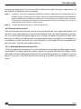
ST9 USER GUIDE
inc R19 ; increment the same register again
The following table summarizes the use of the srp instruction and its effect in terms of group
selection.
Table 1. Register Page Number Summary
Hexadecimal
register
number
F0-FF
E0-EF
D0-DF
C0-CF
B0-BF
A0-AF
90-9F
80-8F
70-7F
60-6F
50-5F
40-4F
30-3F
20-2F
10-1F
00-0F
Notes:
Decimal
register
number
240-255
224-239
208-223
192-207
176-191
160-175
144-159
128-143
112-127
96-111
80-95
64-79
48-63
32-47
16-31
00-15
Function
Paged registers
System registers
General
purpose
registers
Register group
decimal
(hexadecimal)
15 (F)
14 (E)
13 (D)
12 (C)
11 (B)
10 (A)
9
8
7
6
5
4
3
2
1
0
srp #n
instruction to select a
group to provide r0-r15
srp #30
srp #28
srp #26
srp #24
srp #22
srp #20
srp #18
srp #16
srp #14
srp #12
srp #10
srp #8
srp #6
srp #4
srp #2
srp #0
Though it is possible, it normally makes no sense to set the working register group either to
group E (14) or F (15), since the registers in these groups have pre-defined meanings. You cannot use them to store intermediate values of calculations without greatly affecting the behavior
of the microcontroller in an unpredictable way. However, bit-level instructions are only available
using working register addressing, so when you need to do bit manipulations in these groups,
setting the register pointer to either 28 or 30 is an efficient way of programming when accessing
these two groups.
The srp instruction is the only one you have to use to switch register groups, and is the way
working registers are used in most programs. However, the working register scheme includes
a subtlety that is seldom used, but that could give you even more flexibility in some cases. This
is what is described in the next paragraph.
The same register group number can be selected by an odd or even number. In fact, the formula is:
srp
2*n+1
; for group n
srp
2*n
; for group n
or
19/146
ST9 USER GUIDE
3.1.6.2 Defining Two Separate Groups of Eight Working Registers
In this mode, the srp instruction is not used. Instead, we use the pair of instructions srp0 and
srp1. When using a working register, r0 to r7 address the first to the eighth register of the
whole group selected by half the value in RP0 i.e. all the registers of the half group selected by
RP0. Registers r8 to r15 relate to the first to the eighth register of the group pointed to by RP1.
Here is how the two blocks are selected:
Figure 8. Register Numbers
R255
Group F
paged registers
R240
R239
Group E
system registers
R233 Register pointer 1 (RP1R)
R232 Register pointer 0 (RP0R)
R224
R223
R216
R215
R208
R207
Upper part of Group D
as working
register group
r15
r8
Lower part of
group D
RP0R loaded
using the
instruction code
srp0 #2
Groups 2 to C
R32
R31
General Purpose
Registers
R24
R23
R16
R15
Upper part of
group 1
Lower part of Group 1
as working
register group
Group 0
R00
20/146
RP1R loaded
using the
instruction code
srp1 #27
r7
r0
ST9 USER GUIDE
As an example, if RP0 is set to half group 2 (lower part of whole group 1) and RP1 to half
group 27 (upper part of whole group 13), r0 will designate R16 (2 x 8 + 0) while r15 designates
R223 (27 x 8 + 7).
Using either method depends on the organization of the data in the register file. You may find
it convenient to use two 8-register blocks if you need to make quick calculations on pairs of
data that are far apart in the register file.
The page numbering and switching instructions are summarized below:
Table 2. Register Page Number Summary
Hexadecimal
register
number
F8-FF
F0-F7
E8-EF
E0-E7
D8-DF
D0-D7
C8-CF
...
78-7F
...
20-27
18-1F
10-17
08-0F
00-07
Decimal
register
number
248-255
240-247
232-239
224-231
216-223
208-215
200-207
...
120-127
...
32-39
24-31
16-23
08-15
00-07
Function
Paged registers
Paged registers
System registers
System registers
General
purpose
registers
Eight-Register
block decimal
(hexadecimal)
31 (1F)
30 (1E)
29 (1D)
28 (1C)
27 (1B)
26 (1A)
25 (19)
...
15 (0F)
...
4
3
2
1
0
srp0 #n (or srp1) #n
instructions to select a block to
provide r0-r7
and r8-r15 respectively
srp0 or srp1 #31
srp0 or srp1 #30
srp0 or srp1 #29
srp0 or srp1 #28
srp0 or srp1 #27
srp0 or srp1 #26
srp0 or srp1 #25
...
srp0 or srp1 #15
...
srp0 or srp1 #4
srp0 or srp1 #3
srp0 or srp1 #2
srp0 or srp1 #1
srp0 or srp1 #0
When you use an 8- or 16-register group, you may very likely have a subroutine or an interrupt
routine that uses a different set of working registers. You must save (push) the pair of register
pointers RPP that include RP0 and RP1 at the beginning of the routine and restore them on
exit.
3.1.6.3 Peripheral Register Paging
Group F of the 16-register groups is paged so that as many as 64 different groups can be
mapped to this address range. This large space is used to accommodate the registers related
to the peripherals. The paging technique allows you to add any number of peripherals and still
be able to handle them without using up more addresses in the register space.
When you access a register in group 15, first set the Page Pointer Register to the number of
the page that contains the register you want. Here is how a page is selected:
21/146
ST9 USER GUIDE
Figure 9. Selecting Page Registers
R255
Group F
Paged Registers
PPR loaded using
instruction code spp #3.
Page 3
R240
R239
Group E System Registers
R234
Page Pointer Register (PPR)
R224
Groups 0 to D
R00
As with the working registers, if a subroutine or an interrupt routine needs to access a peripheral that uses paged registers (which is very likely), you must save (or push) the register
pointer PPR at the beginning of the routine and restore it on exit.
Notes:
In both assembly and C languages, include files are supplied with symbolic names pre-defined
for all the peripherals. These names are unique for each peripheral; however several different
names relate to the same register, but in a different page. You must bear in mind that writing for
example (in C language):
S_ISR = 0; /* clear serial peripheral error register */
does not automatically select the proper page; this statement must be preceded by another one
that selects the SCI page. Since no predefined C statement exists for this, a convenient way is
to define an assembler statement under the form of a macro that will read nicely in the C source.
An example of the correct way to access the SCI register is:
#define SelectPage(Page) asm ("spp %0":: "i" (Page)) ; /* pseudo function
to select a page */
SelectPage( SCI1_PG );
/* Select the serial peripheral page */
S_ISR = 0 ;
/* Clear serial peripheral error register */
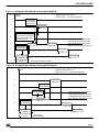
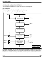
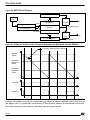
3.1.7 Memory Management Unit
Like most microcontrollers, the ST9 has a bus for interfacing internal and external memories.
This allows you to store both programs and data. A special feature of the ST9 is that it can address a 4 Mbyte single space to address ROM, RAM, EPROM, EEPROM, FLASH.
22/146
ST9 USER GUIDE
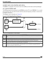
To address the 4 Mbytes of memory, the address bus is 22 bits wide. To manage the 22-bit
address with 16-bit direct or indirect addressing, the memory mechanism adds extra bits to the
16-bit address and then works with segments (see Figure 10) or pages (see Figure 13). The
memories are arranged in 64 segments of 64 Kbytes for the program and in 256 segments of
16 Kbytes for data.
A set of special registers is used to extend the 16-bit address. Programs use the CSR, DMA
uses the DMASR or ISR and interrupts use the ISR or CSR register to provide the 6 Most Significant Bits to make a 22-bit address. Data uses a set of four registers (DPR0-3) to provide
the 8 Most Significant Bits to make a 14-bit address.
Data can be addressed in the Program segment by using special move instructions: lddp,
ldpp, ldpd, lddd.
It is easier from a hardware point of view to use only one address space for Program and
Data.
Figure 10. Addressing via CSR, ISR and DMASR
16-bit Virtual Address
MMU Registers
CSR
DMASR
1
2
1
Fetching program
instruction
2
Data Memory
accessed in DMA
ISR
3
6 bits
3
Fetching interrupt
instruction or DMA
access to Program
Memory
22-bit Physical Address
23/146
ST9 USER GUIDE
3.1.7.1 Program Segment
We can consider this memory as linear since we can jump anywhere in memory space using
the special JPS, CALLS and RETS instructions.
The 6-bit CSR register is used to extend the 16-bit address to a 22-bit address by concatenation (see Figure 10). To make a fast branch in the same segment, use the common JP, CALL
and RET instructions.
To branch to another segment using a far call, the use of CALLS saves the current PC value
and the CSR value (Code Segment Register) in the stack, before loading the PC and the CSR
registers with the new values. Every time the segment changes you have to use the far branch
even if you branch from address (n)FFFFh to (n+1)0000h. This is because the program
doesn’t manage the 6 high-order bits of the 22-bit program addresses if you don’t use a far
branch to change the CSR register value. The script file (described in the Development Tools
chapter) allows you to place all your program modules anywhere in a single segment.
The far branch instruction adds only 2 to 4 additional cycles compared to a near branch instruction.
Note:
In C language, using the small code model (this means only one 64 Kbyte segment is used), all
calls use local branches. If more than one segment is used, the large code model is required
and all calls use far branches even when branching locally. To avoid far calls in the same segment, the segment to be called has to be declared as static if it is not called from another segment.
3.1.7.1.1 Segment and Offset in Assembler Mode or C Language
The Offset represents the address in the segment with 16 bits. If the Segment and the Offset
are known, the following syntax is used for the far branches:
jps
segment,offset
; 6 bits + 16 bits
jps
symbol
; 22 bits
calls
segment,offset
; 6 bits + 16 bits
calls
symbol
; 22 bits
calls
(R),(rr)
; 6 bits + 16 bits
calls
(r),(rr)
; 6 bits + 16 bits
rets
; 22 bits
The assembly tools accept a set of directives which retrieves the elements of a function address or of a label.
The operator SEG (stands for SEGment) allows you to extract the segment number of a label;
similarly, the operator SOF (stands for Segment OFfset) allows you to extract the offset of a
label within its segment.
24/146
ST9 USER GUIDE
These operators are especially useful when applied to a function or instruction label, although
the macro-assembler and assembler do not verify the type of the label.
Example:
ld
r0,#SEG Function
; extract the 6-bit segment
ldw
rr2,#SOF Function
; extract the 16-bit offset
calls
(r0),(rr2)
The same functions exist in C language: SEG(Function); SOF(Function).
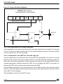
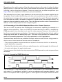
3.1.7.2 Interrupt Service Routine Segment
One program segment is reserved for storing the Interrupt Service Routines. All the interrupt
routines start in this segment.
To obtain a 22-bit address, the 16-bit address is concatenated with 6 bits from the ISR register
(the 6 bits from the ISR register are the high-order bits of the address).
To offer compatibility with the previous ST9 versions and to have a new powerful address
mechanism, you can select “ST9” mode using the EMR2 bit in the ENCSR register.
Both modes use the concatenation of the ISR register value and the 16-bit address as shown
in Figure 10 to address the interrupt vector.
Then, in “ST9” mode, only the ISR register value is used during the interrupt routine. So it’s not
possible to jump to another segment from the Interrupt Service Routine because the CSR register value is not saved with the FLAGR value and the current PC value when the interrupt occurs. The advantage of “ST9” mode is to reduce stack memory usage and CPU cycles by not
saving the CSR value (see Figure 11). This figure shows you the different mechanisms that
are used when an interrupt occurs, when a branch or a call is executed during the interrupt
routine and when the return from interrupt instruction (RETI) is executed.
25/146
ST9 USER GUIDE
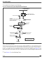
Figure 11. Interrupt Processing in “ST9” Mode
6-bit
6-bit
ISR
6-bit
ISR
6-bit
ISR
CSR
22-bit
8 bits
at ’0’
22-bit
16-bit
Interrupt
Vector
8-bit
Interrupt
Service
Routine
Address
22-bit
22-bit
16-bit Address of
any branch
IVR
16-bit
16-bit
PC MSB
STACK
FLAG
PC MSB
PC LSB
When an interrupt occurs, the 8-bit
IVR address is extended to 22-bits
to obtain the address of the
Interrupt Service Routine
as shown above.
PC LSB
STACK
FLAG
PC MSB
Only the
PC value
is saved
for a
CALL
instruction
FLAG
FLAGR register
PC MSB
PC LSB
STACK
PC LSB
Addresses of local branches
(within the same segment as
the Interrupt Service Routine,
using the CALL instruction) are
extended to 22-bits as shown
above.
Return from interrupt.
The current PC value saved in the
stack and the CSR value are
concatenated to make the 22-bit
return address.
In “ST9” mode, saving the CSR value allows you to change its value to branch to another segment. When the interrupt occurs and when the current PC, CSR and FLAGR values are
saved, the ISR register value is stored in the CSR register (see Figure 12).
26/146
ST9 USER GUIDE
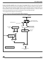
Figure 12. Interrupt Processing in “ST9” Mode
Next segment for
a far branch
6-bit
6-bit
ISR
6-bit
CSR
CSR
CSR
6-bit
ISR
22-bit
22-bit
8 bits
at ’0’
22-bit
16-bit
Interrupt
Vector
8-bit
Interrupt
Service
Routine
Address
22-bit
16-bit Address
of any branch
16-bit
16-bit
IVR
CSR
STACK
FLAG
CSR
PC MSB
PC LSB
CSR+PC
represent
the 22-bit
current address
saved.
STACK
PC MSB
FLAG
PC LSB
CSR
FLAG
CSR
PC MSB
PC LSB
FLAGR register
STACK
PC MSB
PC LSB
When an interrupt occurs, the 16-bit
Interrupt Vector is extended to 22-bits
as shown above.
Before loading the CSR register with
the ISR value, the CSR value is saved
in the stack.
Addresses of local and far
branches (to any segment) are
extended to 22-bits as shown
above.
For a far CALL, the CSR value
is saved with the current PC value
in the stack and the CSR
register is loaded with the new
segment to jump to.
Return from interrupt.
The current PC value and the
CSR value saved in the stack are
concatenated to make the 22-bit
return address.
3.1.7.3 DMA Segment
To address the total 4 Mbytes of memory in a DMA transaction, the DMASR points to a
64-Kbyte segment. Since there is no need to have more than one segment at the same time
for the transaction, the DMA uses a single 64-Kbyte segment instead of 4 pages like a Data
Segment (see below). To use the DMASR register, the DP bit in the DMA Address Register
(DAPR) must be set. If DP is reset, the DMA uses the ISR register instead of the DMASR register.
27/146
ST9 USER GUIDE
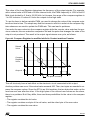
3.1.7.4 Data Segment
Data uses the page mechanism to address the 4 Mbytes of memory.
To authorize data coming from different 64-Kbyte segments, a set of 4 Data Page Registers
(DPR0 to DPR3) allows you to address 16 Kbytes per register (see Figure 13). The DPR is selected with the 2 high-order bits of the 16-bit data address:
DPR0: from 0000h to 3FFFh (b15-b14=00)
DPR1: from 4000h to 7FFFh (b15-b14=01)
DPR2: from 8000h to BFFFh (b15-b14=10)
DPR3: from C000h to FFFFh (b15-b14=11)
After you select the DPR, the 8-bit value of the selected DPR register is used to extend the 14
remaining bits of the address to 22 bits.
For example, if DPR0 equals 20h and DPR1 equals 2h, each memory access in the range of
0000h to 3FFFh uses the DPR0 page and addresses data from 080000h to 083FFFh, and
each memory access in the range of 4000h to 7FFFh uses the DPR1 page and addresses
data from 008000h to 00BFFFh (see Figure 13). For example:
16-bit address = 0010 0101 1010 0101 = 25A5h
0000h < 25A5h < 3FFFh
DPR0 is selected, so the 6 high-order bits are equal to 20h
22-bit address = 0010 0000 10 0101 1010 0101
DPR0 value, 14 LSB of the 16-bit address
= 00 1000 0010 0101 1010 0101 = 0825A5h
With this mechanism, if the 16-bit addresses are different only on the 2 highest bits and if all
the DPR registers selected with these two bits have the same value, the resulting 22-bit address will be the same.
Four pages of 16Kbyte of data memory are enough for many applications and allow you to use
data from different segments without costing additional CPU cycles. With four DPRs, you can
access up to 64K (4 x 16K) of data without changing the DPR values. Data can be variables
stored in RAM or constants stored in program ROM.
The four DPR registers are located in the MMU register page (page 21 of register group F). If
you use them frequently, you can relocate them to register group E, by programming bit 5 of
the EMR2 register (R246 in page 21). This prevents you from having to switch to the MMU
register page from another peripheral register page in order to change a DPR register value.
28/146
ST9 USER GUIDE
Figure 13. Addressing via DPR0-3
16-bit Virtual Address
MMU Registers
DPR1
DPR2
DPR3
00
01
10
11
8 bits
2
M
SB
DPR0
14 LSB
22-bit Physical Address
3.1.7.4.1 Accessing the Page and the Offset in Assembler or C Language
The assembly tools implement a set of operands which allows you to extract the components
of a data address.
The PAG operator (stands for PAGe) extracts the page number of an address; similarly, the
POF operator (stands for Page OFfset) extracts the offset of the address within the page.
Syntax:
PAG label
POF label
Be careful that directly using the data label and using the POF operator on a data label are not
equivalent: the data label gives the 16 bits of the logical label address; the POF operand gives
the 14 lowest bits of the label’s physical or logical address.
Example:
Assuming data is mapped at address 0x129876:
ldw
rr2,#POF data
; rr2 = 0x1876
ldw
rr4,#data
; rr4 = 0xD876 (with DPR3=0x4A)
Remember that you must take care of which data pointer has to be set before accessing a
variable.
29/146
ST9 USER GUIDE
Example:
Assuming that data has been mapped in a page aligned on address 0xC000, this means that
DPR3 will be used, therefore the following code is correct:
ld
DPR3,#PAG data
ldw
rr2,data
ld
r4,(rr2)
In assembly language, it is possible to access data through another DPR:
Example:
Still using data at an address aligned with 0xC000, following code is correct:
ld
DPR2,#PAG data
; if data address=0x01C765, DPR2=7
ldw
rr2, #(POF data)+0x8000; rr2=0x8765
; #(POF data) to reset bit 15 and 14
; and 0x8000 to use DPR2
ld
r4,(rr2)
; indirect addressing mode
...
ld
r4, (POF data)+0x8000 ; direct addressing mode
It is important to look at the explicit usage of the immediate addressing mode (#) to get the
page number and the offset; it is consistent with the ST9 assembly syntax shown in the following example:
ldw
rr2,#Var
ld
r4,(rr2)
...
ld
r4, Var
The same functions exist in C language: PAG(data); POF(data);
30/146
ST9 USER GUIDE
3.2 STACK MODES
The ST9 allows you to have two separate stacks: a system stack and a user stack. The core
uses the system stack in interrupt routines and subroutines to save return addresses, the flag
register and the CSR depending on option (EMR2 register bit Enable Code Segment Register). You can also use it under program control to save data, using the push and pop instructions.
The user stack works exactly the same way, using the pushu and popu instructions but only
under program control, which means that the user stack is not changed by the system. You
may choose to use a separate space for your data, or to store them in the same stack as the
return addresses.
Both stacks can independently be located either in RAM or in the register file. You select this
using the SSP and USP bits in the MODER register (R235) for the system stack and the user
stack, respectively. A low bit value selects a RAM stack, and a high bit value selects a Register File stack.
Since the stacks grow towards low addresses, the stack pointers must be initialized to the
highest location plus one (3) of the space reserved to it. This location becomes the “bottom” of
the stack. When the stack is located in the register file, take care that it does not overwrite
other data, in particular the registers located in groups 14 (0EH) and 15 (0FH). For this reason
it is advisable to set the system stack pointer to the end of group 13 (0DH).
The last register of this group being R223, the instruction that sets the stack pointer will be:
ld
Note 1:
sspr, #224 ; set stack pointer to one above end of group 13
Using two separate stacks in the same kind of storage (memory or register) area is likely to consume more space than if a single stack is used. So most of the time, only one stack will hold
both return addresses and arguments for functions. You can then use pushu and popu instructions to manipulate data with the convenience of auto incrementing or decrementing the pointer
after each access.
As an example, refer to the C language start-up files which initialize both the user and system
stacks.
The following diagram illustrates the two options for locating the stack: in the register file or in
memory.
(3)
The push instruction decrements the stack pointer before writing the data, so this location
would never be used if set to the top location.
31/146
ST9 USER GUIDE
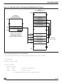
Figure 14. Stack Location Options
R255
R255
Group F
Paged Registers
Group F
Paged Registers
R240
R239
R240
R239
Data Memory
(RAM)
Stack Pointer Low
Stack Pointer High
Group E
System Registers
Stack Pointer Low
Stack Pointer High
Group E
System Registers
Bottom
of Stack
Bottom
of Stack
Stack
Stack
R00
R00
System or User Stack
in Register Space
High byte of pointer irrelevant
System or User Stack
in Data Memory Space
3.3 INSTRUCTION SET
The ST9 is said to be an 8/16-bit microcontroller. This means that although the size of the internal registers and the width of the data bus are 8 bits, the instruction set includes instructions
that handle a pair of registers or a pair of bytes in memory at once. These instructions represent roughly one half of the total instructions, which means that the ST9 can be programmed
with the same ease as if it were advertised as a full 16-bit device.
This is why it is well suited for C programming, as illustrated in this book.
32/146
ST9 USER GUIDE
3.3.1 Overview
For a complete description of the instruction set, you should refer to the ST9 Programming
Manual. The aim here is to give you an introduction to the ST9 instruction set and highlight
some of its best features in terms of power and ease of programming.
Most instructions of the ST9 exist in both byte and word forms. That is, they can operate on either 8 (byte) or 16-bits (word). The mnemonics of the word-instructions all end with a “w”, as
in the following examples:
Load
Add
Subtract
ld
ldw
add
addw
sub
subw
Logical
and
and
andw
Logical or
Compare
Push
Pop
or
orw
cp
cpw
push
pushw
pop
popw
The new powerful instructions added to the ST9 are the CALLS, RETS, JPS instructions for
far branching to change the program segment and the instructions used for C language applications, LINK, LINKU, UNLINK and UNLINKU. Moreover, all instructions have been optimized
compared to Previous ST9.
3.3.1.1 Load Instructions
Beside the classical load instructions found on most microprocessors, there are four special
load instructions for moving data between two locations in memory.
One instruction to move data from data segment to data segment; lddd. This instruction allows you to post-increment the destination and the source index register at the same time. The
ld instruction needs two instructions to do this. An example for moving a block of data would
be:
ld
rr0,#Source
ld
rr2,#Destination
; initialisation of the pointers
ld
r5,#Num_loop
; number of elements to move
ld
r4,(rr0)+
; transfer of one byte
ld
(rr2)+,r4
djnz
r5,loop
loop:
The two ld instructions are coded using 6 bytes and executed in 24 cycles.
The same program with the lddd instruction:
ld
rr0,#Source
ld
rr2,#Destination
; initialisation of the pointers
33/146
ST9 USER GUIDE
ld
r5,#Num_loop
; number of elements to move
lddd
(rr2)+, (rr0)+
; transfer of one byte
djnz
r5,loop
loop:
The lddd instruction is coded using 2 bytes and executed in 14 cycles.
Here are the four possible data transfers:
Instruction
lddd
ldpp
lddp
ldpd
Moves data from...
data segment (uses the DPR0-DPR3 registers)
program segment (uses the CSR register)
program segment
data segment
...to
data segment
program segment
data segment
program segment
These four instructions improve the performance of data block moves (frequently used in C
programs).
As you can see in the table above, the data move can be between data and program segments. Here’s an example of a data move from a Data segment using the DPR register to a
Program segment using the CSR register:
ld
rr0,#Source
ld
rr2,#Destination
; initialisation of the pointers
ld
r5,#Num_loop
; number of elements to move
ldpd
(rr2)+, (rr0)+
; transfer of one byte
djnz
r5,loop
loop:
The data load with rr0 comes from the data segment selected by one of the four DPR register
values depending on the rr0 value and then are stored in the program segment selected by the
CSR register value.
(Please refer to the MMU Section 3.1.7 for an explanation of data and program segments).
3.3.1.2 Test Under Mask
These instructions, tm and tmw, perform a logical (bitwise) AND between the two operands,
but do not store the result. They only set the Z and S bits of the flag register for a later conditional jump on zero or sign. The mask is a value in which the bits that are set to 1 select the
corresponding bits of the value to be tested for non-zero. As an example, in the following instruction:
tm value, mask
34/146
ST9 USER GUIDE
If the mask is a byte whose binary value is 11000000, only the left-most two bits of the unknown value will be tested, and a later branch if zero will be taken or not according only to
these bits. As shown below, the same mask is used for two values that differ only by one bit:
0 0 0 1 1 0 1 0 1
Byte to be tested
1
0
1
1
0
1
0
1
1 1 0 0 0 0 0 0 0
Mask used for testing
1
1
0
0
0
0
0
0
0 0 0 0 0 0 0 0 0
Result of the logical AND operation
1
0
0
0
0
0
0
0
jump taken
Result of the “jump if zero”
jump not taken
Two more instructions, tcm and tcmw, work essentially the same way, but they take the complement of the value to be tested before ANDing it with the mask, as follows:
tcm value, mask
The same two cases will provide the following results:
0 0 0 1 1 0 1 0 1
Byte to be tested
1
0
1
1
0
1
0
1
1 1 1 0 0 1 0 1 0
Complement of the byte to be tested
0
1
0
0
1
0
1
0
1 1 0 0 0 0 0 0 0
Mask used for testing
1
1
0
0
0
0
0
0
1 1 0 0 0 0 0 0 0
Result of the logical AND operation
0
1
0
0
0
0
0
0
jump not taken
Result of the “jump if zero”
jump not taken
The jump would be taken if the byte to be tested had two 1’s in its most significant two bits, for
example 11110101.
3.3.1.3 Push and Pop
Since there are two stacks, there are two kinds of push and pop instructions. The mnemonics
push, pushw, pop and popw act on the system stack, which can be either in the register space
or in the memory space. The mnemonics pushu, pushuw, popu and popuw act on the user
stack, that can also be either in the register space or the memory space. The stack pointer
used in each case is the SSPR or the USPR register pair respectively. The stack pointers are
always decremented before writing on pushing, and they are incremented after reading on
popping. Thus the stack pointer always points to the last byte written. This is worth knowing if
you need to manipulate the stack contents.
The operands to be pushed can be a register, a pair of registers or an immediate value:
35/146
ST9 USER GUIDE
push r6
push (R120)
push #80
pushw RR100
pushw #1500
Pushing an immediate value is especially useful when you are programming in C.
A special push instruction is Push Effective Address. This instruction does not push the data
itself, but the memory address of the data. For example:
pea 5(rr2)
This takes the contents of rr2, adds 5 and pushes the result onto the stack. This is widely used
in C programming.
3.3.1.4 Multiply and Divide
The multiply instruction takes two byte operands and provides a word result. All numbers are
treated as unsigned numbers (operands 0 to 255, result 0 to 65535). Though both operands
are bytes, the first one must address a word to receive the result. The first operand should
then reside in the low byte of the word, and the high byte, not used in the operation, will be
overwritten. The flag register is affected but the state of the flags after the operation is meaningless.
To multiply a signed number (operands -128 to 127) by an unsigned number (operands 0 to
255) with a result in the range of -32768 to 32767, refer to the example given below:
ld
r1,#signed_data
ld
r4,#unsigned_data
btjt
r1.7,neg
mul
rr0,r4
; rr0 = r1*r4, with r1 value a positive signed
; number
jp
end
neg:
mul
rr0,r4
; rr0 = r1*r4, with r1 value a negative signed
; number
sub
r0,r4
; rr0=rr0-100h*r4
end
With the signed operand equal to 226=0E2h (means -30 for signed data) and the second unsigned operand equal to 0Fh (+15) the result will be -450 (0FE3Eh).
36/146
ST9 USER GUIDE
This “eight bits signed by eight bits unsigned” multiplication with a “sixteen bits signed” result
takes a maximum of 36 cycles.
There are two divide instructions.
The div instruction divides a word by a byte, and returns the quotient and the remainder as the
low and the high bytes of the destination respectively. For example:
ldw
rr0,#31184
; rr0=#31184
ld
r2,#201
; r2=#201
div
rr0,r2
; rr0=1D9Bh, 1Dh=#29 and 9Bh=#155
This puts the value 155 in r1 (the quotient) and the value 29 (the remainder) in r0, and r2 still
contains 201.
If the divider is greater than the dividend, nothing is done. If the divisor is zero, a trap is triggered that acts like an interrupt request, and uses the vector at locations 2 and 3 in program
memory. It is up to you to write the appropriate code to handle this trap. Finally, the numbers
to be divided should be such that the quotient be less than 256, that is, can be stored in a
single byte. Otherwise, the results are undefined.
The usable result is only the data stored in r1 which is 155 (for the previous example), the remainder must be divided by the divisor (201) to give more precision (16-bits precision).
ldw
rr0,#31184
; rr0=#31184
ld
r2,#201
; r2=#201
div
rr0,r2
; rr0=1D9Bh, 1Dh=#29 the remainder and
; 9Bh=#155 the quotient
ld
r4,r1
; r4=9Bh=#155
clr
r1
; rr0=1D00h
div
rr0,r2
; rr0=0BC24h, 0BCh=#188 the remainder and
; 24h=#36 the quotient
ld
r0,r4
; rr0=09B24h, 09B24h means in fix-point
; with the point in the 16-bits middle
; 09B24h=155.140625 instead of
; #31184/#201=155.1442786
In the best case, the number of cycles required to divide a word by a byte with 16-bits precision is 80 cycles. This program has to manage overflow and divide by zero functions in order
to be able to be used.
The divws instruction performs one of the sixteen partial divides required to divide a double
word by a word, so you need to write a subroutine to perform the division completely. An example subroutine is given in the ST9 Programming Manual.
37/146
ST9 USER GUIDE
3.3.1.5 Bit Operations
Microcontrollers are often used for controlling inputs and outputs on a single-bit basis, in order
to read the state of a contact, switch a relay on or off, etc. Because of this and because the
data is stored in bytes, instructions for bitwise manipulation of data are welcome.
The ST9 provides instructions to load, and, or, exor, set, clear, complement and test single
bits. These are bld, band, bor, bxor, bset, bres, bcpl, btset.
To designate a single bit in a byte, the notation .n is used. For example, r0.3 means bit 3 of r0.
Here are examples of bit manipulation instructions:
bld
r0.2, r6.4
; bit 4 of r6 copied to bit 2 of r0
bld
r0.3, !r6.0
; complement of bit 0 of r6 copied to bit 3 of r0
band
r0.2, r0.3
; r0.2 contains now (r6.4) and not (r6.0)
bor
r0.2, r2.7
bset
r0.0
; bit 0 or r0 set to 1
bcpl r0.1; bit 1 of r0 is complemented
All the above instructions act on single working registers. If the source operand is preceded by
‘!’, the complement of the source bit is used.
To test a bit, to condition a later jump, we have already described the tm and tcm instructions.
There is another instruction, btset, that can act on either a single or a double working register,
and that sets the Z bit of the FLAGR register if the designated bit is zero. After which, the bit
is set to one. You can use this instruction in an interrupt service routine to test for a request
and acknowledge it in a single instruction.
Warning. Don’t use the bit manipulation instructions directly on bidirectional ports. To avoid
unwanted modifications to the port output register contents, use a copy of the port register,
then transfer the result with a load instruction to the I/O port. (Refer to the Input/Output Bit
Configuration section in the Device Datasheet for more details.)
3.3.1.6 Test and Jump
The btjf and btjt instructions test if a bit is set or cleared respectively and branch to another
program location if true. For example:
btjt
r1.5,Lampon
bset
r1.5
; switch lamp on
Lampon:
...
; continuation of the program
Two instructions are well-suited for implementing lookup tables. These are cpjfi and cpjti. They
compare a byte in a register with a byte pointed to by a register pair, and increment the pointer
38/146
ST9 USER GUIDE
if the condition is not met. If the condition is met, the pointer is not incremented and the branch
is taken. Example:
; Find the position of a letter in a text.
Message:.ascii "This is a trial"
ld
rr0,#Message
; where to search
ld
r2,#'t'
; the character to search for
r2,(rr0),Search
; this is the search loop
Search:
cpjfi
...
; here rr0 points to the 11th character of message
...
; continuation
3.3.1.7 Far Branch
As explained in Section 3.1.7, the 4-Mbyte memory is a segmented memory. It is not possible
to reach another segment with the common CALL, RET and JP instructions because they do
not manage the CSR (Code Segment Register) register. This is managed by the three new
CALLS, RETS and JPS instructions. Only 2 to 4 cycles are added to the common instructions.
3.3.1.8 Optimized C Instructions
In C functions when a function is called, the compiler needs to push the variables in the user/
system stacks and to keep the return address location of the function inside the stack.
Therefore, a frame pointer is used, and 2 pieces of code named prologue and epilogue need
to be added by the C Compiler at the beginning and at the end of the function respectively.
The LINK and UNLINK instructions (LINKU, UNLINKU to use the user stack) are used to reduce the code overhead generated by the compiler inside the function. These instructions are
automatically added by the C Compiler instead of prologue and epilogue (if option -mlink is
specified).
The number of cycles gained by using these instructions is about 34 to 42 cycles and 8 bytes
per called function.
39/146
ST9 USER GUIDE
3.3.2 Advantages when Using C Language
The ST9 has been designed with high-level languages in mind. In particular, the instructions
described above are of special interest to C programmers.
First, as a structured language, C typically uses the stack to pass arguments to functions, return values from functions, and store the local variables of the functions. An instruction such
as:
pushw #1500
pushes a constant integer value as the constant argument of a function. This is used in the following example:
/* define a function that has a single argument of int type */
void MyFunction ( int Param ) ;
{
/* body of the function */
}
void main ( void ) ;
{
/* some code ... */
MyFunction ( 1500 ) ;/* invoke this function with a constant argument */
/* more code ... */
}
Since C makes heavy use of pointers, the instruction:
pea 4(rr2)
pushes the address of the 5th byte of a structure.
For example:
/* define a structured type */
struct sMyStruct {
int N1 ;
int N2 ;
char C1 ;
};
struct sMyStruct MyStruct ;/* create a variable of the above defined type
*/
40/146
ST9 USER GUIDE
/* define a function that has a single argument of type pointer to character
*/
void MyFunc ( char * Arg ) ;
{
/* body of the function */
}
void main ( void ) ;
{
/* some code */
/* invoke the function with the address of the character element of the
structure */
MyFunc ( &MyStruct.C1 ) ;/* &MyStruct.C1 = 4(rr2) if rr2 contains the
address of MyStruct */
/* more code */
}
The lddd, ldpp, lddp, ldpd instructions are used for block copies such as assignments of structures, etc.
Powerful addressing modes such as indirect, indirect with increment or decrement and indexed shorten the code needed to access data even in structures or arrays. They also facilitate access to local variables created on the stack on entering functions. Working registers
that benefit from the most powerful instructions and addressing modes are heavily used by the
compiler. In fact, the GNU9 compiler does not always translate the source code as suggested
above. There are optimization schemes that save execution time and/or memory by judiciously allocating the working registers, so that in many cases arguments are not pushed to
the stack, but merely to an available working register.
3.4 INTERRUPTS
The interrupt system of the ST9 is very powerful, and, in consequence, requires some thorough study to get the most out of it. However, it is worth learning since it allows you to build
very efficient programs with excellent interrupt response times.
The ST9 interrupt system works the same as that of any microcontroller, except for two points
that call for special attention: the vector mechanism and the priority mechanism(4).
(4)
Device Datasheet; Interrupts § 4.
41/146
ST9 USER GUIDE
3.4.1 Interrupt Vectors
Unlike most microcontrollers, the ST9 uses a two-level indirect interrupt vector system. This
means that each peripheral able to generate interrupt requests has a vector register that
points to a location in program memory (the vector array). This location contains the address
of the start of the interrupt service routine. This allows each peripheral to generate several different interrupt requests: the peripheral vector register points to an array of pointers to routines, each routine responding to a different interrupt cause. All pointers to interrupt processing routines, except the Reset, must be located in the first 256 bytes of the Interrupt Service Routine (ISR) segment (one of the 64 code segments). The trap for divide by zero with
the associated far call to the Interrupt Service Routine has to be repeated in all memory segments containing programs that perform division. Code may also reside in this 256-byte
space, provided that it does not overlap with the interrupt vectors.
Figure 15 shows the complete mechanism of the 22-bit address construction from the interrupt
which provides the Interrupt Vector Register value to the return from interrupt.
For each peripheral, the layout of the vector array is specified in the section related to its own
Interrupt Vector Register.
42/146
ST9 USER GUIDE
Figure 15. Interrupt Vectors
(2)
CSR
22-bit
Memory Space
CSR from stack
PC from stack
At the end of the Interrupt Service
Routine, the IRET instruction returns
to the program in the segment
selected by CSR (CSR_5 to CSR_0)
Interrupt Program
22-bit
22-bit
ISR
Segment
ISR or CSR(1)
6-bit
Interrupt Service
Routine Address
8-bit
16-bit
00
ISR
8-bit
ISR Address of
Divide by Zero Trap ISR 0002
ISR 0000
XX FFFF
Paged Registers
01 0000
00 FFFF
Segment
0
R255
ISR Address of
Divide by Zero Trap 00 0002
ISR Address of
Only for the first
RESET
00 0000
segment
Interrupt Vector
Register (IVR)
R240
Divide by zero trap
repeated at each
segment
Bit D0 of IVR is always 0
since the addresses of the
interrupt service routine
start at even addresses
(1) If the ENCSR bit of EMR2 is set (Enable Code Segment Register), the CSR is saved in the stack and then
loaded by the ISR. If it’s reset, the CSR is not saved and only the ISR is used.
(2) If the ENCSR is set, the CSR is reloaded with the value saved in the stack when the interrupt occurs.
If it’s reset, CSR is used instead of ISR when the RETI instruction occurs (Return from interrupt).
As an example, let’s take the ST92F150 Multifunction Timer 0. The registers that define the
MFT0 functions are all contained in pages 9 and 10 of register group 15 (0FH). Register 242,
called the Interrupt Vector Register (IVR), holds the address of the beginning of the vector
array in program memory. The IVR has the following bit layout:
43/146
ST9 USER GUIDE
T0_IVR (R242 page 9)
V4
V3
V2
V1
V0
W1
W0
'0'
Where V4-V0 (fixed by software) are the high bits of the low byte address memory where the
vector for the first interrupt cause is located. Since there are three different interrupt causes,
and the address of each interrupt service routine occupies two bytes, the IVR must be loaded
with an address between 8 and 250 that is a multiple of 8 (i.e. the lower three bits are zero).
The layout above shows two bits W1 and W0 (fixed by hardware), and a third bit that is permanently set to zero. The two W1-W0 bits code four different possible interrupt causes, as in
the following table:
W1
0
0
1
1
W0
0
1
0
1
Interrupt Source
Overflow/ Underflow event interrupts
Not available
Capture event interrupts
Compare event interrupts
When an interrupt occurs, the resulting value is an address that is the value written in IVR
(here 40H), plus the value coded by the cause (if the cause is a capture event, W1-W0 are 10,
thus the value is 4).
This gives an even number, since the least significant bit is zero, as follows:
V4
0
V3
1
V2
0
V1
0
V0
0
W1
1
W0
0
0
0
So IVR points to address XX 0044H (with XX the ISR segment number), which must contain
a word that is equal to the address in the ISR segment of the Interrupt Service Routine for that
cause.
An example of the code for setting the IVR is:
void ConfigTimer0 ( void )
{
/* setting other registers... */
SelectPage (T0C_PG) ;
T0_IVR = (unsigned char)INTRELOADVECT ;/* Array of pointers to service
routines in ROM */
/* setting other registers, continued... */
}
44/146
ST9 USER GUIDE
Figure 16. Interrupt Vectors: Example with Multifunction Timer 0
Memory
(16-bit address space)
65535
Group F
Paged Registers
(8-bit address space)
ISR on
compare event
R255
ISR on
capture event
ISR on
OVF/ UNF event
R242
Interrupt vector register (IVR)
contents = 40h
page 09
R240
The value 40h as the base
address of the interrupt
vector table is chosen
arbitrarily by the programmer
47h
46h
45h
44h
43h
42h
41h
40h
ISR address on
compare event
ISR address on
capture event
Not available
Interrupt
Vector Table
ISR address on
OVF/ UNF
00h
The corresponding source code could be:
; This program uses the 3 interrupt possibilities of MFT0
; Constants
IT_MFT0_VECT = 40h
; Vector table
.section.text
.org
00h
; (default address)
.word
Reset
; reset vector
; if needed divide by zero, NMI vectors
-
45/146
ST9 USER GUIDE
.org
IT_MFT0_VECT
.word
isr_ovf_unf; ISR address on OVF /UNF
.fill
1,2,0xffff ; does not exist in MFT0 interrupt ; skip one vector
.word
isr_capt
; ISR address on capture event
.word
isr_comp
; ISR on compare event
; somewhere in the initialisation code...
;MFT0 initialisation
mft0_init:
spp
#T0C_PG
; select MFT0 control register page
; setting of some other registers...
ld
T0_IVR, #IT_MFT0_VECT; pointer for the vector table
; continuation of the program...
A similar scheme applies for all other peripherals, though the number of interrupt causes may
vary, and thus the size of the pointer table.
Note:
46/146
To summarize, the table of vectors to an interrupt service routine in ROM for a given peripheral
is itself pointed to by the Interrupt Vector Register of this peripheral that must be set to the proper value. This gives you an unusual degree of flexibility: a peripheral may have different interrupt
service routines at different times, without the need to add tests at the beginning of the interrupt
service routine. Let’s consider for example that we want to transfer a string of data from a peripheral. When the first byte of data comes in, we must initialise some variables to handle the
string. Then, all subsequent transfers merely copy the data from the peripheral to memory and
increment the pointer. Switching between these two modes is very easy. Initially, the IVR of the
peripheral is set to the block of vectors that point to the interrupt service routine that serves the
first time. This interrupt service routine changes the value of the IVR to another block of vectors
and returns. The next interrupt will be automatically re-routed to the other, lighter, interrupt service routine. This reduces the execution time of this routine, since we do not need to test whether this is the first time that the interrupt service routine is called or not.
ST9 USER GUIDE
3.4.2 Interrupt Priorities
In any microprocessor-based system, there is a trade-off between the computational power of
the main program and the interrupt latency time. Expressed simply, the less the main program
is disturbed, the sooner it finishes its job. On the other hand, we often need to serve interrupt
requests generated by the peripherals as quickly as possible. Since this is a trade-off, we
need to find a compromise that gives both enough power to the main program while still
keeping it as responsive as possible to interrupts. It is likely that we will need to modify this
compromise according to the current status of the program.
If we define that some interrupt requests are more urgent than others, we can define a priority
or a hierarchy of interrupt requests. The main program itself, if given a priority level, should be
considered as having the lowest priority (except sometimes when interrupts are undesirable).
In most cases, when the main program is running, it can be interrupted by any interrupt request. But once a request is being served, it most likely needs to continue undisturbed, unless
a request from a higher priority level occurs. Then, the higher priority request is served until
completion. The service routine then returns to the lower priority interrupt service routine, that
terminates and eventually returns to the main program. In the ST9, this behavior is called
Nested Mode.
Other types of behavior may be required depending of the kind of processing. For this, the
ST9 interrupt system has two Boolean parameters to select the way interrupts are handled,
which allow four basic choices.
The priority mechanism is driven by the Current Priority Level parameter. At a given time, the
part of the program being executed runs under a certain level. You can change this CPL by
writing a different value in the core’s Central Interrupt Control Register (CICR). You can assign
Priority Level (PL) to each interrupt source. At initialisation time, this value is written in one of
the control registers specific to the corresponding peripheral.
Note:
The PL is a three-bit word that ranges from 0 to 7. Note that 0 stands for a high priority and 7
for a low priority. These bits belong to one of the configuration registers of each peripheral.
When a peripheral requests an interrupt, the built-in interrupt controller compares the priority
level of the interrupt request to the Current Priority Level. The interrupt is only acknowledged
if its priority level value is strictly less than (higher priority) than the Current Priority Level
value. This allows you to filter out interrupt requests according to their degree of importance or
of urgency according to the current activity of the program. The Non-Maskable Interrupt input
(NMI) is hard wired with a higher priority than any level, and thus is acknowledged immediately
in all circumstances.
The ST9 offers two modes for managing interrupt priorities:
– Concurrent Mode
– Nested Mode
47/146
ST9 USER GUIDE
The difference between them is explained below.
3.4.2.1 Global Interrupt Enable Flag
In both modes, when an interrupt request is acknowledged, the Interrupt ENable (IEN) bit is
cleared, preventing the interrupt service routine from being interrupted again until it is finished.
If required, you may prefer to keep it cleared for the duration of the routine or to set IEN at
some place in the routine using the ei instruction. In the first case, if an interrupt request of a
sufficient priority level is received, it will only be serviced as soon as the service routine currently running returns. In the second case, the same interrupt request is serviced as soon as
both it occurs and the IEN bit is set. In short, interrupt service routines may be re-interrupted
or not, at will.
3.4.2.2 Concurrent Mode versus Nested Mode
Selecting either Concurrent Mode (automatically chosen on reset) or Nested Mode changes
the way the Current Priority Level is managed.
In Nested Mode, the CPL is automatically set to the priority of the current interrupt service routine, and is reset to the previous value on return. This allows you handle the interrupt request
according to priority at all times, since during the execution of the service routine for a given interrupt, only those interrupts whose priority is strictly higher than that of the one currently being
served will be taken into consideration. Then if, as must normally be done, the IEN bit is set
during the current service routine, it will be interrupted at once if an interrupt request of higher
priority occurs. If the IEN remains cleared for the whole duration of the service routine, those
interrupt requests will be served first after the current routine has returned.
48/146
ST9 USER GUIDE
Figure 17. Example with Nested Interrupts Enabled
0
Priority
Level
1
Nested mode: IAM bit =”1”
IEN is set to “1” by the programmer
Interrupt #2
is requested
and served
2
Interrupt #2
CPL = 2
3
Interrupt #6 is requested
but not served because
its priority is lower than
the current CPL
4
5
Interrupt #5
is requested
6
ei
Interrupt #5
CPL = 5
Interrupt #5
CPL = 5
Interrupt #6
CPL = 6
ei
7
Interrupt #2 has priority level 2
Interrupt #5 has priority level 3
Interrupt #6 has priority level 6
Main program has priority level 7
Main program
CPL is
(automatically)
di
ei
set to 7
ei
Main program
CPL = 7
(Interrupt #5 can be served)
Figure 18. Example with Nested Interrupts Disabled
0
Priority
Level
Nested mode: IAM bit =”1”
IEN is not set to “1” by the programmer
1
2
Interrupt #2
CPL = 2
Interrupt #2
is requested
3
Interrupt #6
is requested
4
5
6
Interrupt #5
is requested
Interrupt #5
CPL = 5
Interrupt #2 has priority level 2
Interrupt #5 has priority level 3
Interrupt #6 has priority level 6
Main program has priority level 7
Interrupt #6
CPL = 6
7
Main program
CPL is
(automatically)
(Interrupt #5
set to 7 ei can be served)
di
Main program
CPL = 7
49/146
ST9 USER GUIDE
In Concurrent Mode, the CPL is set exclusively by the programmer. You can change it if you
need to shift the compromise mentioned above either towards main program efficiency, or towards short interrupt latency times. So you can have a high-priority service routine that is reinterrupted by a low-priority interrupt request, if the CPL has been set to a low priority and the
IEN bit is set. This mode gives you maximum flexibility, but it is the most difficult to use since
you must keep track of every combination of interrupt requests to achieve the efficiency you
expect from your program.
Figure 19. Example with Concurrent Interrupts Enabled
0
Interrupt #4
is requested
1
2
3
Interrupt #2 and #6
are requested.
The Interrupt #2 is
served first because
it’s priority is higher
than the interrupt #6
Interrupt #2
CPL=7
6
Interrupt #5
CPL=7
ei
7
CPL=7
Interrupt #4
CPL=7
Interrupt #5
is requested
Interrupt #4
CPL=7
Interrupt #5
ei
CPL=7
Interrupt #6
CPL=7
Main program
CPL is set to 7
Interrupt #2
ei
4
5
Interrupt #4 is
served first because
it’s priority is higher
than the interrupt #6
Main
Interrupt #2 has priority level 2
Interrupt #4 has priority level 4
Interrupt #5 has priority level 5
Interrupt #6 has priority level 6
Main prog has priority level 7
CPL=7
Concurrent mode does not look like a reasonable way to handle interrupts if you enable interrupts in your interrupt service routine. It should be thought of as a way to fully control priorities
through programming, if nesting priorities cannot meet your processing requirements. For example, let us consider the case when a timer produces a periodic interrupt that outputs some
data on an external digital to analog converter. The requirement is that the new data be output
at the very time of the interrupt, so as to reduce the jitter (or parasitic frequency modulation)
that would compromise the spectral purity. Then, once the data is output, the interrupt service
routine does some processing to make or get the data for the next interrupt. The latter part of
the processing is much less critical in terms of execution time, provided it is finished before the
next timer interrupt. Using Concurrent mode, you can assign that interrupt the highest priority
so that it will be served immediately, then re-enable the interrupts and, if needed, give it a pri-
50/146
ST9 USER GUIDE
ority level as appropriate. The service routine will then allow other interrupts to gain control, at
the expense of delaying its own completion.
Note 1:
In practice, Concurrent mode does not differ much from nested mode if the interrupts are not reenabled during an interrupt service routine. Concurrent Interrupts Disabled looks like Nested Interrupt Disabled with the difference that the CPL is changed only by software when necessary.
The interrupt requests pending while the interrupt service routine is executing, will only be serviced after the current service routine returns.
Note 2:
An interrupt with priority level 7 will never be served.
3.4.3 External Interrupt Unit
This is a functional block that can receive interrupt requests from up to eight external pins, and
also from some internal devices such as the Watchdog Timer, the Serial Peripheral Interface,
etc. It is used to select the active edge for pin or device, and define the priority for each of the
four pairs. In addition, an NMI pin can be programmed as being maskable or non-maskable. It
is maskable on reset, and once set to non-maskable, it cannot again be set to maskable until
the next reset. This works as explained below.
3.4.3.1 Maskable External Interrupt Pins
These are eight external inputs you can set individually to rising-edge or falling-edge sensitive,
and masked. You assign priorities by pairs, making four groups with different priorities. Within
each group, the two interrupt requests have two successive priorities. For example, if you set
group C to priority 2, the INT4 input will have priority 2 and INT5 will have priority 3 (which is
lower).
51/146
ST9 USER GUIDE
The simplified block diagram is the following:
Figure 20. External Interrupts Simplified Block Diagram
External Interrupt pin
(INT0 to INT7)
Edge trigger event
selection: one bit of EITR
Internal interrupt
Only for:
A0: INT0 or WDT interrupt
B0 INT2 or SPI interrupt
(Device dependent)
Internal/External
source selection
One bit of
EIPR
Pending Bit
One bit of
EIMR
Current priority
level (CPL)
Mask Bit
3
Priority
Comparator
3
External interrupt
priority level
Bit IEN of CICR
Interrupt enable
A detailed block diagram
is provided in Section 7
Interrupt to
the core
3.4.3.2 Top-Level Interrupt
The Top Level Interrupt can have two sources: either the NMI pin, or the watchdog end-ofcount(5). This interrupt level has a special feature that allows you to mask it like any other interrupt, or to make it a real non-maskable interrupt. For this, the TLNM bit (see Figure 21) can
remove the effect of the mask. Once set, it cannot be reset, thus preventing this interrupt from
(5)
See Section 4.3 on the Watchdog Timer.
52/146
ST9 USER GUIDE
being accidentally masked even in the case of a program failure. In any case, the Top Level
Interrupt uses the third fixed vector at addresses 4 and 5 in program memory. As the name implies, it has a fixed priority that is higher than any other interrupt request. Though it does not
clear the IEN bit when acknowledged, unlike all other interrupt requests, its service routine
cannot be interrupted by any cause, including the Top Level Interrupt itself.
The simplified block diagram is the following:
Figure 21. Top-Level Interrupt Simplified Block Diagram
NMI pin
Edge trigger event
selection: one bit of EIVR
Watchdog timer
End of Count
Two bits of
CICR
Watchdog/NMI
source selection:
one bit of EIVR
Interrupt bit
Interrupt enable:
Pending Bit
One bit of
NICR
One bit of
CICR
Top Level not
maskable
A detailed block diagram
is provided in Section 7
Top Level Interrupt to
the core
53/146
ST9 USER GUIDE
3.4.3.3 External Interrupt Vectors
There are eight external interrupt causes. They are each connected to an external input that is
the alternate function of an I/O port. Some of these are shared with other causes in an exclusive manner, i.e., the INT0 pin is multiplexed with the Watchdog/Timer interrupt request, and
the INT5 pin is multiplexed with the Serial Peripheral Interface interrupt request (on the
ST92F150). Each cause is associated with a separate vector in Program Memory. All vectors
are contiguous, generating an array of 8 vectors starting with the INT0 vector, and ending with
the INT7 vector. This array may be freely located in program memory between addresses 8 to
240 (0F0h) in program memory.
These interrupt causes are grouped by pairs, and are given new names inside the interrupt
controller, as shown in the following table:
Interrupt Source
INT 0
INT 1
INT 2
INT 3
INT 4
INT 5
INT 6
INT 7
Interrupt Cause
INT A0
INT A1
INT B0
INT B1
INT C0
INT C1
INT D0
INT D1
You can independently assign a priority to each pair (A, B, C, D), with levels that are multiple
of two, i.e. you can set them to priority levels 0, 2, 4, or 6. In each pair, the cause bearing the
figure zero assumes this priority, and the cause bearing the figure 1 assumes the next level
above. For example, if you assign level 4 to pair C, this means that INTC0 will have level 4 and
INTC1 level 5. You set this in register EIPLR (R245 page 0), where each group of two bits
gives the level of the corresponding interrupt cause.
The interrupt vectoring is summarized in the table below:
54/146
ST9 USER GUIDE
Figure 22. External Interrupt Vectors
7
EIVR (R246, Page 0)
External Interrupt Vector Register
V7 V6
V5
0
V4 TLTEV TLIS IAOS EWEN
1111b Lo
ISR address for INTD1
1110b Hi
V7
V6
V5 V4
MSB of the
Vector Table address
for the
8 external interrupts
(Software fixed)
0111b Lo
ISR address for INTB0
0110b Hi
Vector Table:
(Addresses less than FFh)
0011b Lo
ISR address for INTA1
0010b Hi
0001b Lo
ISR address for INTA0
0000b Hi
LSB of the Vector Table address
for the 8 external interrupts
(Hardware fixed)
55/146
ST9 USER GUIDE
3.5 DMA CONTROLLER
3.5.1 Overview
One of the most important advantages of the ST9 is its ability to handle input/output data flows
without using core instruction cycles. This is made possible by the built-in DMA controller.
Once properly initialized, it allows peripherals to exchange data either with memory or the register file, with no more use of the core resources than the stolen memory cycles strictly needed
to transfer the data.
To see how much faster DMA is than the simplest interrupt service routine, let us compare the
execution times.
Let us assume that the data comes from the serial port. The simplest interrupt routine is the
following:
GetOneByte:; interrupt latency:
22 cycles
push
PPR
; save current page
8
pushw
rr0
; save rr0
10
spp
#SCI_PG
; change register page
4
ldw
rr0, POINTER
; get pointer
12
ld
(rr0)+, S_RXBR
; move data
12
ldw
POINTER, rr0
; store pointer
14
popw
rr0
; restore rr0
10
pop
PPR
; restore current page
8
; return
16
iret
; ------------------------------------------; Total:
116
With an internal clock of 24 MHz, this corresponds to an execution time of 4.8364 µs. In contrast, the DMA cycle time for the transfer of one byte from a register to a register file takes only
8 cycles (16 cycles to the memory), that is 0.33 µs. The DMA feature saves you from using
valuable core processing power for simple tasks like storing an input byte to memory. For example, if a continuous flow of data is input at 19200 bits per second, the interrupt service routine would consume 1.11% of the total cycles of the core, as compared to the 0.0767% with
the DMA solution. Since the DMA is built-in and works with most of the peripherals, it is a good
idea to use it even for slow transfers.
The DMA uses the Segment mechanism to address 64 Kbytes along the linear 4 MBytes. See
Section 3.1.7 for more details.
56/146
ST9 USER GUIDE
3.5.2 How the DMA Works
The DMA consists of a transfer between a memory or register file and a peripheral, in either direction. Assuming the peripheral is configured to handle externally supplied data or to provide
data to external circuits, two steps are needed for a transfer to occur.
The transfer must be requested by some event or condition.
A mechanism must handle reading the data from one part and writing to the other part.
The term DMA transfer represents the transfer of a single byte of data. Usually, more than one
byte is transferred and the transfer occurs in bursts. Thus, a third step is involved:
A mechanism that counts the transfers and stops them when the count is finished.
To the programmer, these mechanisms appear as registers to be properly initialized. The
three steps are handled as follows (see Figure 23).
3.5.2.1 Transfer Requests
The DMA transfer is requested in exactly the same way as an interrupt is requested. According to its type, the peripheral concerned sends a request based on an external event such
as a character received or transmitted by the Serial Channel Interface. You configure this in
the registers belonging to the peripheral involved. Special bits in the registers indicate that the
peripheral ready status, instead of requesting an interrupt, requests a DMA transfer.
3.5.2.2 Transfer Execution
A DMA transfer can involve a memory location or a register in the register file. In any case, the
transfer requires an address and a counter. This address and counter are stored in registers
which you can define anywhere in the register file. The address register value is automatically
incremented after each transfer and the counter register value is decremented so that the next
transfer will involve the next address and this mechanism will continue until the counter is
equal to 0. Depending on whether the transfer addresses memory or the register file, there are
two cases.
If the transfer addresses the register file, the address register and the counter register are
single registers (a byte is enough to address 256 registers). The address of this address register is stored in one of the peripheral's registers, named DCPR. The low bit (RM) of this register is set to zero indicating that the register file is involved in the transfer. The address register must have an even address to address the DMA address, the next register storing the
DMA transaction counter.
If the transfer addresses the memory, the registers that hold the address and the counter must
be two double registers. In this case, the DMA address is pointed by the DAPR pointer register
and the DMA transaction counter is pointed by the DCPR pointer register. The low bit of the
57/146
ST9 USER GUIDE
DAPR indicates whether the memory segment is pointed by DMASR or ISR (see Section
3.1.7). The DMA address and the DMA transaction counter are not necessarily consecutive.
3.5.2.3 Transfer Termination
A burst terminates when the count of transfers reaches a predefined value. To set this up, you
set a counter register in the register file that holds the count of transfers to execute at the start
of a burst. Each transfer decrements it, and the DMA mechanism is stopped when the counter
reaches zero.
The way DMA controller terminates the transfer differs from one peripheral to another, but typically it consists of resetting the bit in the configuration register that tells the peripheral to issue
DMA requests instead of interrupt requests. Then, on the last transfer, when the transfer
counter reaches zero, it toggles the DMA/Interrupt request bit so that the peripheral issues an
interrupt request again. If this request is unmasked, you should vector it to an interrupt service
routine that handles the DMA termination.
To summarise:
For register transfers, the DCPR of the peripheral points to a user-defined pair of registers that
holds the address and the count. Register DAPR is unused. For memory transfers, the DAPR
points to the user-defined register pair that holds the address. The DCPR register points to the
user-defined register pair that holds the count.
Some peripherals, such as the Multifunction Timer, even have a double pair of DAPR/DCPR
registers. Only one pair is used at a time. In so-called Swap Mode, this allows the timer to use
one data buffer for output and another buffer for input. The pair of registers used is automatically changed when one transfer burst terminates, allowing a continuous data flow between
the program and the peripheral, with minimum data handling overhead.
In addition, the MFT has 16-bit registers. Transfers imply two byte transfers for each register.
This is ensured by a mechanism that gives the DMA the highest priority as soon as the first
byte is transferring. This guarantees that the second byte will also be transferred in the
shortest delay, even if other DMA requests become pending while the transfer is in progress.
58/146
ST9 USER GUIDE
Figure 23. DMA Data Transfer
REGISTER FILE
DF
REGISTER FILE
OR
MEMORY
REGISTER FILE
COUNTER
ADDRESS
PERIPHERAL
DATA peripheral
0
Current
COUNTER value
Decrease after
each transfer
Current ADDRESS
Start ADDRESS
59/146
ST9 USER GUIDE
3.6 RESET AND CLOCK CONTROL UNIT (RCCU)
The RCCU is composed of the Clock Control Unit (CCU) and the Reset and Stop Manager.
3.6.1 CLOCK CONTROL UNIT
The CCU generates the peripheral clock INTCLK and the CPU clock CPUCLK. It is a useful
clock generator with low power function and low external frequency oscillator to reduce electromagnetic emissions.
The diagram can be reduced as in Figure 24.
Figure 24. CCU Simplified Block Diagram
1
Quartz
Oscillator
3
4
Clock Multiplier
[1/32 to 14]
5
Prescaler
CPUCLK
CK_AF
Source
2
INTCLK
The CCU is composed of 5 main blocks:
BLOCK
1
2
3
4
5
60/146
COMMENTS
Quartz oscillator gives the main frequency generator. The frequency is in the range of 3 to 5
MHz.
External clock for very low power consumption with a very low frequency.
The Clock Multiplier can reduce or increase the input frequency by using prescaler and
PLL.The increase is for the normal use and the decrease for low power consumption.
The selector aims the clock coming from the Clock Multiplier for normal or low power use or
aims the clock CK_AF for a very low power consumption.
The prescaler is used also for low power consumption. The INTCLK is not change giving a high
frequency to the internal peripheral. This allows the user to slow down program execution
during non processor intensive routines.
ST9 USER GUIDE
3.6.1.1 Clock Multiplier
The Clock Multiplier is a part of the Figure 26.
The advantage of the Clock Multiplier is that it can produce a variable clock frequency depending on the needs of the CPU.
Since the input clock to the PLL circuit requires a 50% duty cycle for correct operation, the divide by two should be enabled (DIV2 bit of MODER register set) if the PLL is enabled. It is necessary when a crystal oscillator is used, or when the external clock generator does not provide
a 50% duty cycle. In practice, the divide-by-two is virtually always used in order to ensure a
50% duty cycle signal to the PLL multiplier circuit.
The Clock Multiplier output is one of the CLOCK2, CLOCK2/16 or CLOCK2*PLLMUL/(DX+1)
(PLLMUL is the PLL multiplier coefficient) frequencies.
The two frequencies CLOCK2 and CLOCK2/16 are for low power consumption or reduce
power consumption, depending on the Wait For Interrupt instruction (refer to the flow chart
Figure 25).
The PLL has four clock multiplier factors (6,8,10 and 14) controlled by the two bits MX0 and
MX1 in the PLLCONF register. The clock divider is controlled by three bits DX0:2 in the
PLLCONF register for seven rates which are 1/(DX+1). Setting DX2:0=7 turns OFF the PLL to
reduce consumption.
When you switch on the PLL, you have to allow a delay for the PLL to lock.
61/146
ST9 USER GUIDE
Figure 25. INTCLK and CPUCLK Flow Chart
Yes
No
WFI
Instruction
No
Yes
CKAF_SEL==0
No
Yes
No
Yes
LPOWFI==0
CK_AF
Present
No
CSU_CKSEL=0
No
Yes
XT_DIV16==0
Yes
WFI_CKSEL==0
No
No
Yes
CSU_CKSEL==0
Yes
CK_AF
Present
No
Yes
Yes
DX2:0==7
CKAF_SEL=0
CKAF_ST=0
CKAF_SEL=1
CKAF_ST=1
No
DX2:0==7
CSU_CKSEL=0
CSU_CKSEL=0
INTCLK=
CLOCK2/16
CK_AF
CLOCK2/16 Previous CK_AF
CLOCK
PLL-CLOCK
CLOCK2 CLOCK2
(PLL OFF) (PLL ON)
CLOCK2/16
(PLL OFF)
Fast mode
LOW POWER
PLL is OFF
CPUCLK Stopped
62/146
Reduced power consumption
Slow mode
Reduced power consumption
CPUCLK=INTCLK/N
ST9 USER GUIDE
Figure 26. Clock Control Unit Programming
XTSTOP
DIV2
CSU_CKSEL
CKAF_SEL
(CLK_FLAG)
(MODER)
(CLK_FLAG)
(CLKCTL)
CLOCK MULTIPLIER
1/16
0
0
Quartz
oscillator
CK_AF
source
1/2
1
CLOCK2
0
PLL
x
6/8/10/14
1/N
MX(1:0)
DX(2:0)
1
1
CLOCK1
0
INTCLK
1
to
Peripherals
and
CPU Clock Prescaler
CK_AF
(PLLCONF)
XT_DIV16
CKAF_ST
(CLK_FLAG)
Wait for Interrupt and Low Power Modes:
LPOWFI (CLKCTL) selects Low Power operation automatically on entering WFI mode.
WFI_CKSEL (CLKCTL) selects the CK_AF clock automatically, if present, on entering WFI mode.
XTSTOP (CLK_FLAG) automatically stops the Xtal oscillator when the CK_AF clock is present and selected.
3.6.1.2 CK_AF Source
When you execute a Wait For Interrupt (WFI) instruction using the Clock Multiplier with output
clock CLOCK2/16, the power is put in Low Power mode. To reduce this power further you
have the possibility of slowing down the INTCLK frequency by using an external clock source
CK_AF. The CK_AF clock will be selected if the WFI_CKSEL bit in the CLKCTL register is set
and if CK_AF is present.
The CK_AF source can also be used in Run mode (no WFI) to reduce power consumption if
CKAF_SEL is set and CK_AF is present.
63/146
ST9 USER GUIDE
3.6.1.3 Low Power with Frequency Slow Down
When the PLL has been frozen by a WFI instruction you need a delay after the interrupt to wait
for the PLL to lock. To avoid this delay but not to lose the Low Power consumption, you have
two choices which are:
– To use a WFI instruction with LPOWFI reset and initialize INTCLK to CLOCK2 with
XT_DIV16 bit set (CSU_CKSEL register). When the WFI occurs, CPUCLK is stopped and
INTCLK doesn’t change.
– To not use the WFI instruction. Set XT_DIV16 bit of CSU_CKSEL register. Initialize DX2:0
of PLLCONF to 6 to divide the PLL output clock by 7 which is the maximum. Initialize the
CPUCLK clock prescaler to 7 to divide INTCLK by 8.
3.6.2 Reset and Stop Manager
RESET normally means restarting from the beginning with everything initialized. However
sometimes it’s necessary to know the context of the ST9 before the RESET and if it was an external or internal RESET. Two bits, SOFTRES and WDGRES in the CLK_FLAG register indicate the previous context. Table 3. shows the three cases to manage.
Table 3. Three Types of RESET
RESET Type
External RESET
SOFTRES bit
0
WDGRES bit
0
Watchdog RESET
0
1
Software RESET
1
0
Meaning
High to low level on RESET pin.
The Watchdog Timer is activated and the Timer
has reached 0.
The HALT instruction is executed, waiting for an
external Reset to restart (if the SRESEN bit in the
CLKCTL register is set).
These bits are read-only and change with each Reset.
64/146
ST9 USER GUIDE
4 USING THE ON-CHIP PERIPHERALS
This chapter introduces the main peripherals of the ST9 family. Each variant includes none,
one or several peripherals of each type. This allows you to select the variant that best fits your
requirements. For high-volume markets, you can order custom versions with exactly the type
and number of peripherals required, including the relatively exotic ones not described here but
available on request, such as videotext decoders etc.
4.1 PROGRAMMING THE CORE AND PERIPHERALS
In addition to describing how each peripheral works, we give examples of the code needed to
use them in several configurations. This code is available on the Companion software. You
can experiment with the original code or modify it to do the functions you require.
Configuring and using the core and the peripherals involves a considerable amount of bit manipulation in the registers. Many variables that drive microcontroller states are Boolean
values. To reduce the use of addressable space in registers, bits have been logically grouped
in bytes, so the majority of the control registers have their eight bits fully used.
To properly program these registers, you need to track the exact position of each bit in each
register. You can do this by referring systematically to the appropriate Data Sheet, and commenting the source text so that it can be easily read and understood later. See the following
example:
ld
R235,#11100000B ; R235 is register MODER
;
|||||||+-- HIMP : no foreign access to bus
;
||||||+--- BRQEN : no foreign access to bus
;
|||+++---- PRS2,1,0 : processor at full speed
;
||+------- DIV2 : crystal frequency divided by 2
;
|+-------- USP : user stack pointer in registers
;
+--------- SSP : system stack pointer in registers
spp
ld
#0
; SPI page
R254,#10000001B
;
|||||||+-- SPR0 : SPR1, SPR0 = 01: clock divided by 16
;
||||||+--- SPR1 :
;
|||||+---- CPHA : Input sampled on rising edge
;
||||+----- CPOL : Rest level of serial clock = 0
;
|||+------ BUSY : Set to ready
;
||+------- ARB : No I²C arbitration
;
|+-------- BMS : SPI used as a shift register (not I²C)
;
+--------- SPEN : SPI enabled
65/146
ST9 USER GUIDE
This style has the advantage of clarity. However, there is still a problem that it does not address: the variety of the different products of the ST9 family.
The different products available in the ST9 family are very diverse and as a result it is not always the case for all products that a given function is performed by the same bit of the same
register. The location of a register in one peripheral may be different in another. To avoid this
problem, the GNU9 programming tool chain provides a set of include files that define the physical location of every bit and register, by their symbolic name. These files correspond to the
appropriate variant of the ST9. Using them guarantees that switching to another member of
the family will not need more than changing the Include statement at the beginning of the
source text. The same example as above, using the predefined symbols reads as follows:
.include "system.inc" ; System register
ld
MODER,#MOm_sspm+MOm_uspm+MOm_div2m; Both stacks in
;registers, clock divided by 2
spp
#SPI_PG
;SPI page
ld
SPICR,#SPm_spen+SPm_SP_16 ; Enable SPI,1st clock
; configuration, Clock/16
This notation is more compact, and is independent of changes either between variants in the
same family, or by changes made globally to the family in the future. This writing style is recommended for this reason.
4.2 PARALLEL I/O
The parallel input-outputs have a basically very straightforward functionality. Once initialized,
they appear as a register that can be written or read. However in many cases, direct byte-wide
input-output is not sufficient. Bit-oriented I/O is often what is used in microcontroller systems.
A powerful feature of the ST9 is that you can address the eight bits of each port individually.
The ST9, like most microcontrollers also provides the external pins of the other peripherals
(timers, UARTs, etc.) by diverting some bits from the parallel I/O ports.
The ST9 parallel I/O has an additional very flexible feature. You can independently configure
each bit as:
– An input with two variants (TTL or CMOS levels)
– An output with also two variants (open-drain or push-pull)
– A bi-directional port with either a weak pull-up or an open-drain output side
– An alternate function output (that is, the output pin of an internal peripheral), with also either
open-drain or push-pull output driver.
66/146
ST9 USER GUIDE
– Analog Input (see note)
Note:
On the port that accommodates the inputs of the Analog to Digital Converter, there is a special
feature. In all other peripherals that require an input, you only need to configure the corresponding pin as an input. However, when using the ADC you can put the input pins to any voltage level
from ground to Vcc. This is normally badly handled by standard logic gates that dissipate considerable power when the voltage reaches the limit range. To avoid this, the port that provides
the input pins of the ADC has a special Alternate Function mode. Unlike the other ports it is used
for input. This mode disconnects the input buffer from the pin and shorts the buffer input to the
ground. The output buffer is put in high-impedance mode. The pin is permanently connected to
the input of the ADC, thus allowing its voltage to be read at any time.
To handle all these capabilities, each port requires three configuration registers, PxC1, PxC2
and PxC3, where x is the port number. Once configured, a port exchanges data with the core
through the PxDR data register.
The configuration registers are placed in various pages of the register group 15, as well as the
data registers, except for the first six ports. These six belong to the system register group
(group 14) for easy access.
Some ports also include DMA capability, configurable to work with the Multi-Function Timer.
67/146
ST9 USER GUIDE
4.3 STANDARD AND WATCHDOG TIMERS
You can use this timer both as a regular timer and as a watchdog timer.
4.3.1 Description
The block diagram of the Watchdog Timer is the following:
Figure 27. Watchdog Timer Simplified Block Diagram
INTCLK/4
WDIN Pin
Input Modes and
Clock Control Logic
3 bits of
WDTCR
2 bits of
WDTCR
Prescaler (8-bit)
16-bit Downcounter
WDOUT Pin
3 bits of
WDTCR
1 bit of
WCR
Output Control
Logic
Reset and
interrupt
request
to the core
INT0 Pin
NMI Pin
Reset and Interrupt
Control Logic
2 bits of
EIVR
A detailed block diagram
is provided in Section 7
In Counter/Timer mode, the WDT can count pulses coming either from an input pin (WDIN; in
the ST92F150, alternate function of P5.3) or from the internal clock divided by 4. When the internal clock is used, the external pin, if enabled, can either gate the clock, start the counter, or
68/146
ST9 USER GUIDE
reload it with its initial value. You select these modes using three bits in the WDT Control Register, as follows:
INEN
1
1
1
1
0
INMD1
0
0
1
1
X
INMD2
0
1
1
0
X
Mode
Event counter mode
Gated mode
Retriggerable input mode
Triggerable input mode
Input section disabled. Internal clock selected.
4.3.1.1 Event Counter Mode
The counter value is decremented at each falling edge on the WDTIN pin if ST_SP is high (bit
7 of WDTCR).
Figure 28. Timer in Event Counter Mode
WDTIN Pin
ST_SP
Counter
Value
4.3.1.2 Gated Input Mode
The counter value is decremented by WDTCLK (INTCLK / 4) if the WDTIN pin and ST_SP are
high.
Figure 29. Timer in Gated Input Mode
WDTIN Pin
ST_SP
Counter
Value
69/146
ST9 USER GUIDE
4.3.1.3 Retriggerable Input Mode
The counter value is decremented by WDTCLK (INTCLK / 4) if ST_SP is high.
The initial value is reloaded either at the rising edge of ST_SP or at each falling edge of the
WDTIN pin if ST_SP is high.
Figure 30. Timer in Retriggerable Input Mode
WDTIN Pin
ST_SP
Counter
Value
Initial Value
4.3.1.4 Triggerable Input Mode
The counter value is decremented by WDTCLK (INTCLK / 4) if ST_SP is high and falling edge
of WDTIN occurs.
The initial value is reloaded at the first falling edge of the WDTIN pin if ST_SP is high.
Figure 31. Timer in Triggerable Input Mode
WDTIN Pin
ST_SP
Initial Value
Counter
Value
70/146
ST9 USER GUIDE
4.3.1.5 Single/Continuous Mode
On counter underflow (End Of Count), the counter is always reloaded with the value of the
latch that is actually accessed when writing to the WDTHR and WDTLR register pair.
The counter has two modes: Single-shot or Continuous, selected by the S_C bit of WDTCR.
In Single-shot mode, the End Of Count also resets the ST_SP bit of the WDTCR, which stops
the counter after one cycle. In Continuous mode on reaching the End Of Count condition, the
counter reloads the constant and restarts. When the ST_SP bit is set, the contents of the latch
are written again to the counter, allowing the initial count value to be changed before starting
the counter.
You restart the down counter by setting the ST_SP bit. The constant value can be either the
initial value or a new one as shown on the following diagram:
Figure 32. Timer in Single Mode
ST_SP
Initial Value
Counter
Value
End of Count
A new value may be written in the counter latches at any time. It will be transferred
into the counter on end of count or on various conditions on WDTIN and ST_SP.
4.3.1.6 Output Pin
Another pin, WDOUT (alternate function of P5.1 for ST92F150), when enabled by the OUTEN
bit, can change its state in two ways on the end of count of the main counter. Basically, each
time the counter overflows, it updates the output value. This can produce two different effects,
selected by the OUTMD bit: either the state of the WROUT bit is copied to the output at that
time, or the output is complemented.
71/146
ST9 USER GUIDE
Figure 33. Output Pin Block Diagram
WDTCR (R251 page 0)
Timer/Watchdog Control Register
0
7
ST_SP S_C INMD1 INMD2 INEN OUTMD WROUT OUTEN
Logical level user definable
while counter is running
1
D
WDTOUT
Pin
0
EOC
4.3.2 Timer Application for Periodic Interrupts
In this application, the clock is internal and the input and output pins are unused. The counter
is set to Continuous mode, and the value of the reload registers chosen so that the overflow
occurs exactly every 128 microseconds.
4.3.2.1 Initialisation of the WDT for a Periodic Interrupt
Very few registers are involved when you use the WDT for this purpose, since there is no input
apart from the internal clock and no output. However, the WDT interrupt handling is a little different from most other peripherals in that it borrows the interrupt circuit named INTA0 that is
normally assigned to external interrupt pin INT0. So you configure the WDT in two steps: initializing the WDT itself, and also the external interrupt INTA0.
In this example application, the internal frequency is 24 MHz and the interrupt rate must be
8192 Hz. The timer starts with the preset count on the low-to-high transition of the ST_SP bit
of the WDT Control Register.
The initialisation routine for the WDT is then:
72/146
ST9 USER GUIDE
/* *********** Configure Watchdog for Periodic Interrupt *************/
void ConfigWDT ( void )
{
SelectPage( WDT_PG )
;/* select Watchdog page */
WDTPR = 0 ;/* 122 us = 366 ticks */
WDTR = 365 ;/* preset is nb ticks-1 (WDTR is the pair WDTLR and WDTHR) */
WDTCR = (WDTm_stsp) ;/* WDT is set to continuous mode, no inputs, no
outputs */
/* Interrupt must be connected to intA0 in the EIVR register */
}
The initialisation routine for INTA0 follows. In this example application, interrupt A0 is the only
"external" interrupt enabled, and it is assigned priority level 2:
/* ***********Initialise Interrupt A0 and Current Level **************/
void ConfigInterrupts ( void )
{
SelectPage( EXINT_PG ) ;
EIVR = (EIm_tlism+(unsigned char)INTA0VECT) ;/* int. A0 is generated
on WDT overflow */
EIPLR = 1 ;/* intr A0 (and that of same group) with high priority */
EIMR = EIm_ia0m ;/* intr A0 alone enabled */
CICR = (Im_gcenm+Im_iamm+Im_ienm)+7 ;
/* current processing level: minimum ; int. enabled, nested mode */
/* This starts also the MFT */
}
4.3.3 Watchdog Application 1: Generating a PWM
This application provides a PWM with a programmable duty cycle. You can use it as an application exercise for learning to use the programming and debugging tools since it is very
simple. The only hardware required to watch the effect of the program is a LED in series with
a resistor connected between P4.4 and Vcc (anode towards Vcc). You will find the application
in the Companion software in the WDT/appli1 directory.
The WDT can only provide a delay after which the output may change its state, and an interrupt is triggered. The principle of using the WDT as a rectangular signal generator is to set it
to Continuous mode, to load it with a time value, and let it count down until zero. The control
register is set so that an interrupt is then generated, and the output pin is updated at the same
time. The interrupt service routine will reload with the other value, and preset the WROUT bit
to the complement of the current value, so that the opposite state will be transferred to the
73/146
ST9 USER GUIDE
output pin at the next end of count. By alternating between two time values, a duty cycle other
than 50% can be obtained (PWM). When the interrupt occurs, the output has already changed
its state, so that the waveform can be very precise since it depends only on the timer hardware
and not on the software. All that the interrupt service routine has to do is to load the timer latch
with the value to be used when the end of count is reached. Thus, the constraint is that the reload interrupt must be guaranteed a latency time less that the shortest time between two
output transitions. This may or may not be difficult to realize according to the intended timing
and the presence of portions of the program where the interrupts are disabled. It is thus recommended to properly manage the interrupts and thoroughly use the priorities to achieve this
requirement.
The WDT does not have an interrupt cause and a vector of its own. It must borrow them either
from the Top Level Interrupt or the INTA0 input. We have chosen to use INTA0 here, and to
give it a priority of 6 which is high, but not the highest (which is 0).
4.3.4 Watchdog Application 2: Using the Watchdog
A watchdog timer is a safety measure to prevent a program going adrift. It relies on a hardware
timer that must be periodically reset by the program. Failing to do this will reset the whole program (at the End Of Count). You will find it in the Companion software in the WDT/appli2 directory.
The efficiency of this approach varies with the type of program and depends on the following
conditions:
The hardware action to perform in order to reset the timer must be so complex that if the processor goes adrift, it cannot accidentally reset the watchdog. In the ST9, you need to write
0AAh and 055h successively to the WDTLR.
The chosen time-out value must be greater than the interval at which the program resets the
watchdog. It must also be as close as possible to that interval for maximum safety. Since the
watchdog time-out value is set once at the beginning of the program, this condition is best fulfilled if the resetting action is performed at constant intervals.
A special software arrangement must be designed to reduce the chance that the part of the
program that resets the watchdog can continue undisturbed when other parts of the program
are faulty. This may include an interlock mechanism that requires that several program
branches be executed to enable the resetting of the Watchdog count.
As you can see, achieving a very secure program malfunction detection by the sole means of
a watchdog is a very difficult thing to realize. However, the watchdog can still play a key role
in the safety of some systems, an example of which is an induction motor controller.
74/146
ST9 USER GUIDE
4.4 MULTIFUNCTION TIMER
This device is the most powerful of the ST9 on-chip peripherals. This description only covers
its main features. You can study the more intricate details with the help of an ST9 Datasheet.
The Multifunction Timer can handle many different operating modes; so many in fact, that virtually the only limit is your imagination. Let’s first have a look at the general organization.
The first diagram in Figure 34 represents the inputs and outputs, the prescaler register and the
clock selection blocks, with their associated configuration registers.
75/146
ST9 USER GUIDE
Figure 34. MFT Input/Output Modes
TxINA pin TxINB pin
Input pin
configuration
4 bits of
ICR
Input pin function
4 bits of
ICR
Internal clk/3
3 bits of
TCR
2 bits of
TCR
CLK logic
U/D logic
Clear logic
8 bit prescaler
Clock
U/D
Clear
16 bit counter of the MFT
Action on outputs
after a successful event on
<Cmp0> <Comp1> <OVF>
2 bits of
TMR
(output enable)
5 bits of
FLAGR
8 bits of
OACR
8 bits of
OBCR
Output pin configuration
TxOUTA pin
TxOUTB pin
The two outputs are actually the Q outputs of a flip-flop which set and reset. Flip-flop inputs
can be individually configured to receive pulses from either of the following events: compare
with CM0, compare with CM1, and overflow/underflow. This is used to generate single-shot or
periodic wave forms simply by using the timer.
76/146
ST9 USER GUIDE
In addition to providing output signals, the timers can generate so-called “internal events” that
can be used to synchronize other internal peripherals such as the DMA and the Analog to Digital Converter. Not all peripherals to be synchronized can be connected to just any MFT. For
each ST9 variant, the connection between each MFT and the other peripheral is unique. Refer
to the corresponding datasheet for more information.
The second block diagram represents the counter, the capture and compare registers, the reload logic and the associated configuration and status registers. The interrupt and DMA blocks
are not represented.
Figure 35. MFT Simplified Block Diagram
6 bits of
TMR
Load/Capture/Monitor
Logic
Capture/Load Register 0
2 bits of
FLAGR
(result:)
Capture/Load Register 1
Clock
16-bit Counter
with Comparator
U/D
(result:)
Clear
1 bit of TCR
(OVF/UNF)
Counter
Enable
Compare 0 Register
1 bit of TCR
1 bit of CICR
Compare 1 Register
Compare Logic
(result:)
2 bits of
FLAGR
VR02111J
In the above diagrams, the interrupt and DMA logic are not represented. They obey the general interrupt and DMA rules described earlier, and are controlled by three registers.
The Interrupt Vector Register controls the location of the interrupt vectors in program memory.
They must be located at addresses that are multiples of 8.
77/146
ST9 USER GUIDE
Figure 36. MFT Interrupt Vector Register
IVR (R242 page 9 MFT0) (R246 page 9 MFT1)
Interrupt Vector Register
7
0
V4
V3
V2
V1 V0
W1 W0 D0
Not used
MSB of the vector
address table, fixed
by software inside the
interrupt vector table
LSB of the vector address table, fixed by hardware
Interrupt Source
0
0
1
1
0
1
0
1
Overflow/underflow event interrupts
Not Available
Capture event interrupts
Compare event interrupts
The Interrupt and DMA Mask Register individually enable and disable the various interrupt
and DMA sources.
Figure 37. MFT Interrupt and DMA Mask Register
IDMR (R255)
Interrupt / DMA Mask Register
7
0
GTIEN CP0D CP0I CP1I CM0D CM0I CM1I 0UI
OVF Interrupt Mask
Compare 1 Interrupt Mask
Compare 0 Interrupt Mask
Compare 0 DMA Mask
Capture 1 Interrupt Mask
Capture 0 Interrupt Mask
Capture 0 DMA Mask
Global Timer Interrupt Enable
The upper five bits of the Interrupt and DMA Control Register indicate the status of the interrupts and the DMA blocks. The lower three bits set the Interrupt and DMA priority level.
78/146
ST9 USER GUIDE
Figure 38. MFT Interrupt and DMA Control Register
IDCR (R243, Page 9, MFT 0) (R247, Page 9, MFT 1)
Interrupt/DMA Control Register
7
0
CPE CME DCTS DCTD SWEN PL2 PL1 PL0
Interrupt/DMA Priority Level
The Input and Output Control Register has only two active bits. They are used to internally
connect the Output A of each MFT to its own Input A. One bit does this connection for all evennumbered MFTs, and the other for all odd-numbered MFTs.
Figure 39. MFT I/O Control Register
IOCR (R248)
I/O Connection Register
7
0
SC1 SC 0
TxINA and TxOUTA
Internally connected or not
for each even MFT.
TxINA and TxOUTA
Internally connected or not for each odd MFT.
4.4.1 Generating Two Pulse Width Modulated Waves with One MFT
4.4.1.1 Description Example
The Multifunction Timer is used here as a double pulse-width modulator. It is also possible to
have a single PWM output if needed. Let’s look at a simplified block diagram of the MFT
showing only the functional blocks that are actually used. See Figure 40.
This is possible using the two comparators that simultaneously compare each capture register
with the free-running counter. When the counter overflows, it is reloaded with the contents of
the Load Register 0. At that time, both outputs are reset.
When the value of the counter becomes equal to one of the compare registers, a pulse is sent
to the output flip-flop of the corresponding side, thus setting the output. So the low time is the
time between the counter overflow and the comparison. The high time is the remainder of the
period.
79/146
ST9 USER GUIDE
Figure 40. MFT Block Diagram
Compare Register 1
CPU
Clock
Compare Signal
Set
Clock
Prescaler
Comparator 1
Reset
Free-running
Counter
Load Register 0
Full Count
Comparator 0
Overflow Signal
Reset
Set
Compare Register 0
Phase A PWM
Phase B PWM
Compare Signal
Figure 41. Using a Counter and 2 Compare Registers to Modulate 2 Pulse Widths
Current contents of the counter
Reload
Value
Compare
Register 1
Value
Compare
Register 0
Value
Output B
Output A
Actually, as nearly everything is configurable by values in control registers, this is only one of
the ways to do it. In particular, the direction of the counter (upward or downward) and the effect of the actions on the outputs (set/reset) can be chosen at will.
80/146
ST9 USER GUIDE
This value of the Load Register determines the frequency of the output signals. For example,
with a reload value of 255 and a 25 Mhz internal clock, the PWM frequency is 1/256 of the 25
MHz clock divided by 3, that is 32,552 kHz. In this case, the range of the compare registers is
1 to 255 inclusive. A value of 0 locks the outputs to the high state.
To use the timer to deliver variable PWM, we need to change the value of the compare registers from time to time. The simple way that first comes to mind is to write into the compare register whenever we need to update the PWM rate. This can lead to problems.
If we write the new value into the compare register while the counter value matches the previous contents, this can make the comparison fail and the pulse that changes the state of the
output is not produced. The result is the output signal misses one cycle, as follows:
Figure 42. Compare Register is modified while its Content matches Counter
Reload
Value
Compare
Register 0
Value
This comparison has failed
Output A
This pulse is missing.
This will obviously have a bad effect on the electronic circuit connected to this output.
Another problem can occur if the reload value exceeds 255. Then, two bytes are needed to express the compare values. Since the ST9 is an 8-bit machine, the two bytes that make up the
word are sent one after the other. If the high bytes of the old and new values are the same,
there is no problem. But if they differ, there are three possibilities for the value in the compare
register:
– The register contains the old value
– The register contains one byte of the old value, and the other byte of the new value
– The register contains the new value
81/146
ST9 USER GUIDE
Depending on the relative values of the old and new values, on the order of writing the bytes
(high byte first, or low byte first), and on the direction of the timer (up-counting or downcounting), various things may happen. These can range from a missed comparison (see
Figure 42) to two comparisons in the same cycle (not a problem).
This indicates that you have to pay attention to the time at which the compare register has to
be updated. If we consider that the duty cycle does not vary widely from one cycle to another,
the safest time to change value is as soon as possible after the match. The best way to do it
is to store the new value in a variable (a register is a good choice), and configure the MFT to
trigger an interrupt when the match occurs. Then, the interrupt service routine is executed and
the new value is safely copied into the compare register.
4.4.2 Generating a Pulse Width Modulated Wave with a Cleaner Spectrum
The use of a MFT to produce two PWM signals is convenient, especially for example in a
stepper motor application. There, an ST92F150 is used and only one MFT is available for
PWM generation, since the other one is used for other purposes. However, this method suffers from a parasitic phase modulation of the signal since the falling edge is fixed, and the
rising edge moves with the desired duty cycle. This leads to the production of unwanted harmonics in the resulting spectrum. This is not a problem for a lot of applications.
Sometime these harmonics are prohibited. Example: when we want to drive a high power induction motor, these harmonics have two serious drawbacks:
– They produce parasitic frequencies that are injected in the mains, which is not allowed by
power distribution companies,
– They feed the induction motor with even ranked harmonics, which degrade the efficiency of
the motor and reduce the peak output power.
You can improve this situation by using a symmetrical PWM generation, producing waveforms
as follows:
Figure 43. Symmetrical PWM Waveforms
18%
50%
82%
You use the MFT in the following way. One MFT being used for one output signal, you use
only output A. You configure it so that it is set on a comparison with compare register 1, and
reset on a comparison with compare register 0. These registers are always loaded with values
82/146
ST9 USER GUIDE
that are symmetrically centred on half of the reload value. For example, if the reload value is
255, the compare registers are set to the following values:
Duty Cycle
10%
25%
50%
75%
90%
Compare Register 0
115
96
64
32
13
Compare Register 1
140
159
191
223
242
You need to ensure that the compare registers are not written while they are used for a comparison. Because of this, they are written in an interrupt service routine that is triggered by the
MFT itself. To allow maximum latency time, the interrupt is triggered either by a compare 0 or
a compare 1 event, according to the value of the duty cycle. For duty cycles between 0 and
50%, the compare 0 event is used. Between 50% and 100%, the compare 1 event is used.
The following figures shows the timing diagram.
Figure 44. Output A Timing
Reload
Value
Compare
Register 1
Value
Compare
Register 0
Value
Output A
Reload
Interrupt
83/146
ST9 USER GUIDE
4.4.3 Incremental Encoder Counter
An incremental encoder is a device that generates two square signals in quadrature when its
shaft rotates. Its main specification is the number of cycles per revolution, i.e. the number of
square signal cycles for one shaft revolution. The greater the number of cycles, the more accurate it is, and the more it costs.
In a stepper motor application, it is used to monitor the rotation of the motor. Here however, we
have taken an encoder that has a great resolution, and this section will show you how to use
an MFT to count encoder pulses, and rescale it to another resolution to meet your project
needs.
4.4.3.1 Description
The MFT includes an input block, a counter block, an event block and an output block. In this
application, no output signal is required, since the counter is expected to produce a value that
is read in registers.
The MFT must provide the following functions:
– Use the inputs to drive the counter according to the amount and direction of rotation
– Keep the count undisturbed by events other than the transitions at the inputs
– Allow reading the current counter value
– Allow setting the counter to an arbitrary initial value
We configure the input block to use the two square signals delivered by the encoder to drive
the up and down counting of the counter. We do this using a special mode of the input block
called “autodiscrimination”. In this mode, the input pulses clock the counter, and the phase relationship between the two signals selects up or down counting. Since the process is incremental, once the MFT configured this way, it automatically follows the rotation of the encoder
shaft and the counter value reflects its position relative to the position it was in when the
counter was configured. In our example, the encoder produces 512 cycles per revolution. Because the counter is 16-bit, it can monitor shaft positions 65536/512 = 128 (or +/-64) full revolutions from the original position.
To operate with an encoder as the input pulse source, we need to set the MFT to Continuous
Mode. When the counter crosses the FFFF to 0000 boundary in either direction, this is called
an End-Of-Count event. In the normal Continuous mode, the End-Of-Count event reloads the
counter with the contents of REG0R (or REG1R in biload mode). In this application, no automatic reload may occur at any time so we can use the full range of the counter and be able to
cross the boundary. To prevent the reload from occurring, we must set the REG0R register to
Capture Mode. The MFT is then said to be in Free-Running Mode.
We have thus selected Free-Running Mode, yet we need to be able to set the counter to any
arbitrary value that is taken as the initial position. For this we need to use the REG0R register
84/146
ST9 USER GUIDE
as the Load register. The solution is to initialise the MFT with REG0R in capture mode by setting the RM0 bit of the TCR register to ensure Free-Running Mode. When we need to load a
value in the counter, we temporarily clear the RM0 bit. Then we set REG0R to the value that
must be written in the counter. The CP0 bit in the FLAGR register is pulsed high to write the
contents of REG0R into the counter. Then we set bit RM0 again.
4.4.3.2 Initialisation
The code for initializing the MFT is given below.
Note:
The ICR register sets the input to Autodiscrimination mode. In this mode, the lower four bits are
irrelevant.
void ConfigTimer1 ( void )
{
SelectPage (T1D_PG) ;
T_REG0R = 0 ;/* This register is used to preload the counter */
T_REG1R = 0 ;/* This register is used to read the counter */
/* T_CMP0R and T_CMP1R are not used */
T_TCR = Tm_cen ;/* enable counter */
/* The counter will not start until the Global Counter Enable is set in
register CICR */
T_TMR = Tm_rm0 ;/* capture using REG0R and monitor using REG1R */
/* This mode is not desired, but is implies free-running, which we need
*/
T_ICR = Tm_ab_aa ;/* inputs used in autodiscriminating mode */
/* For so, the port 3 must be set to input on pins P3.4 and P3.6 */
T_PRSR = 0 ;/* prescaler rate = 1 */
T_OACR = 0 ;/* output A not used */
T_OBCR = 0 ;/* output B not used */
T_FLAGR = 0 ;/* not used */
T_IDMR = 0 ;/* not used */
}
4.4.3.3 Reading
To read the value of the counter, you need to capture it in one of the registers, since the
counter itself does not have an address and cannot be read directly. There are two ways of
reading the counter:
Set one of the registers REG0R or REG1R to Capture mode. A pulse on bit CP0 or CP1, respectively, transfers the contents of the counter to the corresponding register.
85/146
ST9 USER GUIDE
Put REG1R in Monitor mode. In this mode, REG1R continuously reflects the value of the
counter, without the need for pulsing a bit in a register.
In the stepper motor application, we have chosen to use Monitor mode. No special function is
needed to read the counter. A simple assignment of REG1R to a variable is enough, such as:
Pos = REG1R ;/* Get current counter value */
4.4.3.4 Updating
As mentioned in Section 4.5.3.1, updating requires switching the mode of REG0R from Capture to Load.
/* This function forces the MFT1 counter to a value given in argument */
void SetEncoder ( int Value )
{
SelectPage (T1D_PG) ;
T_TMR &= ~Tm_rm0 ;/* Switch temporarily to "Load with REG0R" mode */
T_REG0R = Value ;/* set encoder */
/* convert motor position to match the encoder's resolution */
T_FLAGR |= Tm_cp0 ;/* Load counter with this value by pulsing CP0 high */
T_FLAGR &= ~Tm_cp0 ;/* Return CP0 to low */
T_TMR |= Tm_rm0 ;/* Go back to "Capture with REG0R" mode that implies
free-running */
}
4.4.4 MFT Application 1: Generating 2 PWMs using Interrupts
This application generates 2 independent PWM signals on pins T0OUTA and T0OUTB provided that a logical low level is applied to gate T0INA. The outputs are reset on compare
events and set on the counter underflow. This application is found in the MFT/appli1 directory.
Counter compare interrupts are used to reload compare registers in order to modify the duty
cycle.
When running one of these three examples on an ST92F150 microcontroller, note that MFT
outputs are pure open drain.
4.4.5 MFT Application 2: Generating a PWM using DMA
This application generates a PWM signal on pin T0OUTA using a DMA channel to transfer
duty cycle data from memory to register COMP0. The DMA transfer only occurs once as it is
not re-initialized in the DMA end of block interrupt routine. This application is found in the MFT/
appli2.
86/146
ST9 USER GUIDE
4.4.6 MFT Application 3: Generating a PWM using the DMA Swap Mode
This application generates a PWM signal on pin T0OUTA using the DMA swap mode to
transfer duty cycle data from memory to register COMP0. This application is found in the MFT/
appli3 directory.
Swap mode uses two sets of DMA registers and swaps from one to the other at the end of
each transfer. The end of block interrupt routine reloads the unused set of DMA registers for
the next transfer.
87/146
ST9 USER GUIDE
4.5 SERIAL PERIPHERAL INTERFACE
4.5.1 Description
The SPI is a synchronous input-output port that you can configure in various modes, including
S-Bus. It can have many more uses, of which two are considered here: interfacing with serialaccess EEPROMs and interfacing with a liquid-crystal display.
The main block of the SPI is an 8-bit shift register which can be read or written in parallel
through the internal data bus of the ST9, and that can shift the data in or out on two separate
pins, named SDI and SDO, respectively. The serial transfer is initiated with a write to the SPI
Data Register (SPIDR). Data is input and output simultaneously with each most significant bit
being output on SDO while the level at SDI becomes the least significant bit. Each time a bit
is transferred, a pulse is output at the SCK pin. When eight bits are transferred, eight pulses
have been sent on SCK, and the process stops. If the proper bits are set in the SPI Control
Register (SPICR), an interrupt can be requested on end of transmission. To summaries:
– Transfers are started by writing a byte into the SPI data register
– Data is input and output at the same time
– Data is input and output with the most-significant bit being sent first
– Eight clock pulses are output on the SCK pin synchronously with bit shifting
– An interrupt request can be issued on end of transmission
The SPI is configured with the SPICR register. Four bits of this register are of special interest
in the applications detailed here: these are the CPOL-CPHA pair, and the SPR1-SPR0 pair.
The CPOL-CPHA pair defines the polarity and phase of the clock pulses. This allows them to
adapt to the external device. CPOL selects between rising edge or falling edge as the active
transition, and CPHA selects whether the first active edge is the first edge of the pulse train or
the second one.
The SPR1-SPR0 pair selects one of four different transfer speeds.
4.5.2 Static Liquid-Crystal Display Interface Example
This example uses a static liquid-crystal display that shows a simple number. This can be the
voltage in a digital voltmeter, or any 3 1/2 digit value. A very simple demonstration program is
supplied in the Companion Software. Some of the routines are reused in the bar code reader
described later.
A static liquid-crystal display is composed of a glass back-panel, and a set of front-panel electrodes printed on a glass front-panel. The space between both panels is filled with a liquidcrystal solution. The electrodes are transparent, and the panels may be fitted with a combination of polarisers, so that the whole display, unpowered, is either transparent or opaque according to the selected polariser combination. When a difference of potential is applied be-
88/146
ST9 USER GUIDE
tween one electrode and the backplane, the area delimited on the front panel by the shape of
the electrode takes the reverse state, i.e. opaque or transparent, respectively. Using a sevensegment pattern, it is possible to display numbers, by activating the appropriate segments to
show the desired figures.
A liquid-crystal display presents a high impedance between its electrodes, ranging typically in
the megaohm region. It is thus a voltage-controlled device, with a threshold of about 3 V to
change from one state to the other. Driving such a display is then a simple matter, but one fundamental precaution must be taken to avoid premature destruction of the display: it must be
driven with alternating voltage, to avoid electrolysis within the inter-electrode solution. The frequency is of little importance, and the best values range between 30 and 100 Hz.
This basic explanation does not cover all the details and precautions relative to LCDs but is
sufficient to understand the use of the SPI as a LCD driver.
In this application, the display is installed on a separate board. Since it has 40 pins, it is not
convenient to connect this board with a 40-wire cable. Using a serial synchronous transmission, only four wires are required. The block diagram of the circuit of the display board is:
Figure 45. LCD Interface Example
Liquid Crystal Display
a
f
e
b
g
d
c
dp
One digit
+1 back panel
Serial Input
Shift Clock
dp g f e d c b a dp g f e d c b a
dp g f e d c b a
32 bit serial input, parallel output shift register
+5V
Ground
As shown by this diagram, to make it easy to wire our display board, the correspondence between the segment positions and the bit positions in the bytes transferred is actually:
Bit position
Segment
7
dp
6
g
5
f
4
a
3
b
2
c
1
d
0
e
And the conversion between the figures (0 to 9) and the display pattern is done by a constant
array defined in this case as:
; Table of characters. Gives the patterns for the last 3 digits, from 0 to 9.
89/146
ST9 USER GUIDE
Characters:
.byte 3Fh, 0Ch, 5Bh, 5Eh, 64h, 76h, 77h, 1Ch, 7Fh, 7Eh
The LCD electrodes are connected to the outputs of a serial input, parallel output shift register.
The backplane is also connected to one output. This allows us to provide the A.C. drive for the
electrodes, as shown in the table below:
Level of the backplane
0
0
1
1
Level of one of the State of the liquid crystal
segments
between the electrodes
0
off
1
on, positive voltage
0
on, negative voltage
1
off
In short, the segment is On if its level is different from that of the backplane. It is Off if its level
is the same as that of the backplane. Thus, to generate the drive pattern, it is only necessary
to build the four bytes that correspond to the various segments, keeping the bit corresponding
to the backplane at level zero. Then, using a periodic interrupt, these four words are transmitted serially, but complemented every other time. As an example, to display the value 375,
as in the demonstration program, the following message is built:
Symbols
00000000
Hundreds
01011110
Tens
00011100
Units
01110110
Since in this original message the backplane bit is kept at zero, all bits that are 1 correspond
to an activated segment; the others remain invisible. This message is sent at intervals of about
16 ms, but it is inverted every other time, giving the succession:
Symbols
00000000
11111111
00000000
11111111
00000000
11111111
etc.
Hundreds
01011110
10100001
01011110
10100001
01011110
10100001
Tens
00011100
11100011
00011100
11100011
00011100
11100011
Units
01110110
10001001
01110110
10001001
01110110
10001001
This succession of inverted words guarantee a zero D.C. component across the liquid crystal
solution, which is absolutely necessary.
90/146
ST9 USER GUIDE
4.5.3 EEPROM Serial Interface Example using I²C
An I²C Serial EEPROM is a very convenient device that stores a few bytes for at least 10 years
in a secure manner. The serial I²C access uses only two wires, which allows the memory to fit
in an 8-pin DIL package. The serial access requires a serial transmission protocol, which
makes the access more difficult than with a parallel-bus EEPROM device. This, however, is
not a real drawback, for two reasons:
– The serial synchronous transmission is very easy to implement, and is not time-critical
– Using a serial protocol makes it impossible (or very unlikely) that you will overwrite or erase
data by mistake, which ensures a high safety level for the application
Thus, for applications that can manage with a small amount of permanent data, a serial EEPROM is the best choice. Examples include storing the reading of a counter or a recording
meter, storing configuration parameters or calibration values. The application described here
uses a 24C08 memory chip from STMicroelectronics, that takes advantage of the SPI to exchange data with minimum software overhead.
4.5.3.1 Additional Clock Timing
Compared to I²C timing, SPI timing needs additional software to manage the following:
– The start condition
– The ninth bit for acknowledgement
– The stop condition
These three timing differences are implemented by changing the input/output port data and
configuration registers, to pull the level on the SDA and SCL pins up or down.
4.5.3.2 EEPROM I²C Protocol
To connect more than one device to an I²C interface, each device needs an address to be selected. The EEPROM 24C08, used for our example, has an address equal to A0h.
Following a start condition, the bus master (SPI) must output the address of the EEPROM it is
accessing. The most significant four bits are the device type identifier (1010). The following bit
identifies the specific memory location on the bus (it is matched to the chip enable signal).
Once the 6th and 7th bits are sent, select the block number and the 8th bit sent is the read or
write bit (1 for read, 0 for write). After the address has been sent, ten data bytes can be sent
to the EEPROM for writing, and all the data bytes can be read successively from the EEPROM
for verification.
91/146
ST9 USER GUIDE
4.6 SERIAL COMMUNICATIONS INTERFACE
4.6.1 Description
The SCI is the association of a UART and a complex logic that handles tasks such as character recognition and DMA. It can also work as a simple serial expansion port that then resembles the SPI. The example given here appears as a classical UART application, viewed externally, but it is assisted by the built-in DMA controller to provide effortless transfers of data in
and out of the application. As serial communication is a feature that is very often used, it will
be found in all three applications.
The SCI has four operating modes:
– Asynchronous mode where data and clock can be asynchronous. Each data is sampled 16
times per clock period. The baud rate should be set to the 16 division mode and the frequency of the input clock is set to suit.
– Asynchronous mode with synchronous clock where data and clock are synchronous but the
transmit and receive clock are asynchronous. The receive clock must be given by the external peripheral.
– Serial Expansion mode where data and clock are synchronous and the clock is supplied by
the transmitter (ST9 in transmission and externally in reception).
– Synchronous mode where data and clock are synchronous, the transmit data clock is supplied by the ST9 and the receive data clock is received by the external peripheral. In this
mode there are no start and stop bits.
These four operating modes allow you to connect the ST9 to any external interface.
4.6.1.1 UART
The UART offers all the usual functions for asynchronous transfer. You can set it to handle
word lengths of 5 to 8 bits, with or without parity, even or odd. It offers also the possibility to append a signalling bit (called Address bit or 9th bit -- regardless of the word length) at the end
of the transmitted data, just before the stop bit. This can be used to help design a multidrop
network. The UART can be set to interrupt the processor only when this bit is high, indicating
that the current character is an address or other identifier. This prevents the processor from
being disturbed by the traffic on the network unless an address byte is received, so that the
processor can check if it is concerned or not by the incoming data.
The UART is set to 8 bits, 1 stop bit and no parity, by writing the appropriate value in the
CHCR register.
A timer is part of the SCI block. It is used as a Baud Rate Generator (BRG). It allows you to divide either the internal clock or the frequency available at the RXCLK input pin, by an arbitrary
value. This output can be fed to the receive and transmit sections, though each section can
92/146
ST9 USER GUIDE
have its own clock frequency supplied on pins RXCLK and TXCLK for receive and transmit,
respectively. Here, we use the BRG to clock both sections.
At the clock input of the transmit and receive shift registers, two other dividers can be inserted,
to further divide the frequency by 16. It must be used in Asynchronous mode to allow detection
of the start bit using a local clock. If an external clock is supplied, at the same frequency and
phase as the serial incoming data, the 16x divisor must not be used. Here, the predivisor is
used.
The UART is surrounded by logic that allows it to detect errors on reception, a break state on
the line, and also to recognize a match between the character received and a reference character stored in a register. This last feature is used here. The ACR register is loaded with the
value 10 representing the LF character, and the IMR interrupt mask register is set to enable an
interrupt on a character match. Since DMA is used to transfer the incoming characters to
memory, this technique is used to detect the end of message, if we state that all commands
must end with an LF character.
4.6.1.2 DMA Controller
The DMA is used for the automatic data transfer from memory or a register to the serial transmitter or from the serial receiver to a register or memory, or both.
The working of the DMA in conjunction with the UART merits some detailed explanation, because it is subtle and you need to take some precautions to make it work properly. Once initialized, it is easy to use and it consumes very little computing power to initialise transmission
or re-enable reception.
The DMA transfers in each direction are controlled by two registers: the DMA transaction
counter and the DMA pointer. The transaction counter is used to stop the transaction when a
predefined number of characters is transferred. The DMA pointer points to the character to be
sent or to the location that will hold the next character to be received. To initialise a DMA
transfer, the transaction counter must be set to the number of characters to be transferred and
the DMA pointer must be set to the beginning of the storage area that contains the data to be
transmitted or that will hold the data string received.
Transfers can occur between the UART and either the memory or register file.
The transaction counter and the DMA pointer must be registers in the register file. If the register file is involved in the transfer, both the transaction counter and the pointer must be single
bytes (the addressing range of the register file is 0 to 255). If the memory is involved, the
counter and the pointer must be each a pair of registers, since the addressing range in
memory is 0 to 65535 for one segment.
Once you have defined in which registers you will put the counter and the pointer, you must let
the SCI know. The SCI has two registers for this purpose called the DMA Address Pointer
93/146
ST9 USER GUIDE
Register (DAPR) and DMA Counter Pointer Register (DCPR). These registers are not the actual counter and the pointer, they point to where you want to locate them in the register file.
This double pointer mechanism is similar to that described for interrupts.
Here there can be two cases: the transfer involves the memory or the register file.
If the transfer involves the memory, it’s standard procedure. The DCPR points to the 16-bit
Counter register, and the DAPR points to the 16-bit Address register. These two register pairs
may reside anywhere there is room for them in the register file. Since register pairs are used,
their addresses are even. The DCPR must be even. To reach the DMA segment the DMASR
(or ISR depending on DAPR bit 0) MMU register contains the segment number.
If the transfer involves the register file, things are a bit different. Both the transaction counter
and the address register are 8-bit values. They are supposed to be adjacent in the register file,
i.e. they occupy two successive registers: the first one, even numbered, is the address register. The second one, odd numbered, is the transaction counter. To select this mode, the
least significant bit of the DCPR must be one. Its value is the address of the address register
(which is even) plus one. The DAPR is not used.
The whole mechanism described above applies for both the transmitter side and the receiver
side. Thus, there are twice as many registers as mentioned: the TDCPR and the TDAPR for
the transmitter side, the RDCPR and the RDAPR for the receiver side. The registers you have
located in the register file are also twice as many. So, the TDCPR points to the transmitter
transaction counter and the TDAPR points to the transmitter address register (with the exception mentioned above if the transaction involves the register file). The RDCPR points to the receiver transaction counter and the RDAPR points to the receiver address register.
When a DMA transfer is in progress, the processor is not even aware of it (except that it is
slightly slowed down by the stolen clock cycles). So nothing special has to be done as far as
the program is concerned. The question is: how to start and end a DMA transfer? Here, the
processor is involved, and some code is needed. Depending on which side is concerned, the
processes are different.
4.6.1.2.1 Transmitter Side
To start a DMA transmission, you need to do the following operations, in order:
– Set the DMA segment register DMASR (or ISR) to point to the selected segment of data
memory.
– Set the transmit address register to the address of the second word to be sent (not the
TDAPR, which is only set once at initialisation, and points permanently to the transmit address register).
94/146
ST9 USER GUIDE
– Set the transmit transaction counter to the number of characters to be transmitted minus one
(not the TDCPR, which is also only set once at initialisation, and points permanently to the
transmit transaction counter).
– Set the TXD bit of the IDPR register. This bit enables the Transmitter holding register empty
flag (TXHEM bit of register ISR) to trigger a DMA transfer when the last character is sent.
When TXD is reset, the holding register empty flag would trigger an interrupt instead.
– Load the Transmit Buffer Register (TXBR) with the first character to be sent. This starts the
DMA process as soon as this character is transmitted.
– Clear the Transmitter holding register empty flag (TXHEM bit of register ISR) and the Transmitter buffer register empty flag (TXSEM bit of register ISR) to prevent DMA transfer from
starting before the first character is fully transmitted.
– Enable the end of DMA interrupt by setting the Transmitter Data Interrupt Mask (TXDI bit of
register IMR).
The DMA is now started and will stop when the transaction counter reaches zero.
Note:
The transmit address register is initialized with the address of the second word and the transmit
transaction counter is initialized to the number of characters to be transmitted minus one, because the DMA transfer begins when the first word is transmitted (a write in the Transmit Holding
Register), so the first word is transmitted “by hand”.
4.6.1.2.2 Receiver Side
The receiver side is a little more complicated as two kinds of events can occur during reception:
– There can be transmission errors that must be handled.
– A break is received or a character match event can occur.
The receiver is set in a ready for DMA condition by the initialisation code.
Reception normally finishes when the DMA transaction counter has reached zero. But this is
not necessarily the way one wants to use the serial input, since it implies that the number of
characters to be received must be known before the transfer starts. In most cases, charactertype messages have a variable length.
In this application, the transaction counter is not expected to reach zero, since the size of the
buffer assigned for reception exceeds the longest message defined in the specification. Thus,
if the transaction counter reaches zero this is in fact an overflow condition. In this case, the
contents of the buffer are discarded and a new reception is initiated. In both cases, the steps
to perform an End of Block are:
– Reset the Receiver End of Block (RXEOB bit of register IMR) to remove the interrupt request.
– Use the received characters, if required.
95/146
ST9 USER GUIDE
– Re-enable the end of block interrupts by setting the Receive DMA Bit (RXD bit of register
IDPR).
– Restore the DMA capability by setting the receive address pointer (not the RDAPR) to the
address of the beginning of the receive buffer.
– Set the receive transaction counter (not the RDCPR) to the number of characters to be received. This will re-enable the DMA capability.
In a typical application, command messages could have variable length and be terminated by
an LF character. So, the character match event capability built in to the SCI should be used.
If the Address/Data Compare Register (ACR) contains the value 10 (ASCII code for LF), and
the Receive Address Mask (RXA bit of register IMR) is set, whenever an LF character is received, an interrupt is generated. This interrupt is considered in the application as a good Message Received signal. It is processed the following way:
– In this application, no other characters are expected until the previous message has been
answered by the program. However, it may be useful to inhibit further DMA cycles by clearing
the RXD bit in the IDPR register and also the RXDI bit in the IMR register.
– Read the Receive Buffer Register (RXBR) to remove the interrupt request (see note below).
– Make use of the received characters.
– Restore the DMA capability by setting the receive address pointer (not the RDAPR) to the
address of the beginning of the receive buffer.
– Set the receive transaction counter (not the RDCPR) to the number of characters to be received. This will re-enable the DMA capability.
Note:
When matching occurs between the incoming character and the ACR register contents, the
DMA request is not generated, neither is an interrupt request for “character received”. So, the
incoming character remains in the receive buffer and no other character can be received until it
has been removed. This is why it is not sufficient to clear the RXAP bit in the ISR register to
reinstate the DMA transfer. You must clear the RXBR register by reading it during the character
match interrupt service routine.
Finally, an error may occur during transmission. This can be a parity error (if parity checking is
enabled), a framing error or an overrun error. If one of these errors occurs, take the following
steps:
– Clear the bits that indicate an error condition in the ISR register.
– Restore the DMA capability by setting the receive address pointer (not the RDAPR) to the
address of the beginning of the receive buffer.
– Set the receive transaction counter (not the RDCPR) to the number of characters to be received. This will re-enable the DMA capability.
96/146
ST9 USER GUIDE
4.6.1.2.3 Interrupt Vectors
The interrupt vector scheme has been explained in Section 3.4.1 using the example of the
MFT to illustrate the mechanism. Here is the equivalent table for the SCI giving the position of
the four vectors dedicated to the four interrupt causes.
Value in IVR
50
Address in ROM of the Value of the Pointer to interrupt
selected pointer
routine
Receiver error
50
Address of error processing routine
Address of Address match processBreak detect or address match
50+2
ing routine
Receiver data ready or DMA end of
Address of receive DMA end of block
50+4
block
processing routine
Transmitter buffer empty of DMA end
Address of transmit DMA end of block
50+6
of block
processing routine
Interrupt cause
4.6.2 SCI Application 1: Sending Bytes using Interrupts
This application sends 10 bytes to the USART. An interrupt is generated at the end of every
single byte transmission. During this interrupt routine, the TXBR register is loaded with the
next byte to be transmitted. This application is found in the SCI/appli directory.
The character format is: 2400 bauds, 8 data bits, 1 stop bit and odd parity. Sent bytes can be
received on a PC loaded with a serial communication management software program such as
Hyperteminal.
4.6.3 SCI Application 2: Sending Bytes using DMA
This application sends bytes from the memory to the SCI peripheral using a DMA channel.
The transfer is re-initialized twice in the DMA End of Block interrupt routine so that data is
transmitted three times. This application is found in the SCI/appli2 directory.
4.6.4 SCI Application 3: Sending and Receiving Bytes using DMA
This application sends bytes from the memory to SCI and receives bytes from SCI to the register file using two DMA channels. The SCI cell is configured in loopback so that each byte
sent is immediately received by the SCI. This application is found in the SCI/appli3 directory.
4.6.5 SCI Application 4: Matching Input Bytes
This application receives bytes from the USART and reacts only if an “F” (upper case) is received: on a character match, a “0” is displayed on the 7-segment LED display on port 4. This
application is found in the SCI/appli4 directory.
97/146
ST9 USER GUIDE
4.7 ANALOG TO DIGITAL CONVERTER
4.7.1 Description
The analog to digital converter is one of the simplest peripherals of the ST9 family to use. It
converts the voltage applied to one of sixteen inputs using an 10-bit successive approximation
analog to digital converter. According to the value of bits SC3, SC2, SC1 and SC0 of the Control Logic Register (CLR1, R252, P63), one to sixteen inputs are converted at each conversion
cycle, starting at the channel number specified by these bits and ending with channel 15.
The simplified block diagram is the following:
98/146
ST9 USER GUIDE
Figure 46. A/D Converter Block Diagram
A/D End of conversion or
AWD interrupt to the core
Priority
Mechanism
3 bits of
AD_ICR
1 bit of
AD_IVR
3 bits of
CICR
A/D or AWD
Interrupt Vector
selection
4 bits of
AD_ICR
Pending & Mask bits
4 bits of
AD_CRR
Compare Result
Analog Watchdog
Threshold
registers 16-bit H/L(Ch.A)
Threshold
registers 16-bit H/L(Ch.B)
2
Data
Register
10
4 bits of
CLR1
EXTRG pin
A/D Converter
16
Autoscan Logic
Synchronisation to
Start/Stop the
A/D Converter
AIN pins
channels 0 to 16
See fully detailed
diagram of the
A/D converter in Section 6
4 bits of
CLR1
The conversion cycle can either be started in Single mode, by a trigger (software or hardware,
the later being internal or external) or in Continuous mode, restarted as soon as the previous
cycle is finished.
Each channel uses one bit of a port (the port depends on the variant of the ST9), and the conversion result is stored in a 16-bit register. Sixteen such registers are available, named
AD_D0R to AD_D15R. These 16 bit registers are data registers are made up of two 8-bit reg-
99/146
ST9 USER GUIDE
isters e.g AD_D0R is made up of AD_D0LR (For lower 2 bits of 10 bits result) and AD_D0HR
(For upper 8 bits of 10 bits result).
The end of conversion sets the ECV bit in the AD_ICR register, and can trigger an interrupt request, if the ECI bit (mask of the end of conversion interrupt request) of the Interrupt Control
Register (AD_ICR) is set.
Notes
The internal interrupt controller does not automatically reset the ECV bit. It must be reset by the
interrupt service routine prior to returning from interrupt. Failure to do this would cause the interrupt to loop endlessly.
As mentioned in Section 4.2 on parallel ports, you must configure the corresponding pins to
alternate function both to reduce loading on the analog source and to avoid excessive dissipation in the pin's input buffer. For the same reason, it is advised to keep this I/O configuration if
an analog voltage is present on the pin, even if it is not being converted at this time.
4.7.2 Analog Watchdog
A special feature of this peripheral is the so-called Analog Watchdog. If enabled, the values of
Channel A or both Channel A and Channel B are each compared after each conversion with
a pair of upper and lower thresholds stored in registers AD_LTAR (AD_LTAHR,AD_LTALR),
AD_UTAR(AD_UTAHR,AD_UTALR) for Channel A, and AD_LTBR(AD_LTBHR,AD_LTBLR),
AD_UTBR(AD_UTBHR,AD_UTBLR) for Channel B. Channel A and Channel B are selected
by CC[3:0] bits in control register AD_CLR1.
If the value is outside the threshold values, the AWD bit of the AD_ICR register is set. This can
trigger an interrupt request if the AWDI bit of the same register is set. To know which of the
four thresholds has been exceeded, the Compare Result Register (CRR) has four bits with
one each corresponding to one of these thresholds. The appropriate bit is set when the
threshold has been exceeded.
Notes:
The AWD bit, like the ECV bit, is not automatically reset by the internal interrupt controller. Thus
it must be reset by the interrupt service routine prior to returning from interrupt. Failure to do this
would cause the interrupt to loop endlessly.
To permit power saving in applications where energy conservation is important, you can power
the ADC on and off so that it only consumes power when used. However when you switch it on,
after a delay of 10 µs first conversion starts. The reset condition is off.
4.7.3 Interrupt Vectoring
Two vectors are dedicated to the ADC: the end of conversion vector and the analog watchdog
vector. This allows these two events to be serviced by two different routines. The vectors used
depends on the state of the W1 bit in the AD_IVR register. This bit is set or reset according to
the source of the interrupt.
However, it may occur that both interrupts are generated simultaneously. In that case, analog
watchdog has Priority over End of Conversion request.
100/146
ST9 USER GUIDE
4.7.4 ADC Application: A/D Conversions and Analog Watchdog using Interrupts
This application converts the analog value presented on P7.7 and enters the conversion results in a chart as long as the converted value resides within the user-defined threshold. The
end of conversion interrupt is used to transfer the result of the conversion to the chart. The analog watchdog interrupt, when triggered, stops the A/D converter. This application is located in
the ADC/appli directory.
101/146
ST9 USER GUIDE
4.8 PERIPHERAL INITIALIZATION
All the ST9 peripherals have a large number of configuration options. This makes them highly
adaptable, but has a complex initialization procedure.
To help you to use the peripherals easily, you can find all the initialization programs on the
<http://www.stmcu.com> internet site.
The purpose of these programs is to give you C language programs to get started with programming each peripheral. This program package consists of a Header file, a peripheral function, a startup and a main program for each peripheral.
The startup (crtbegin.spp) and the main (main.c) files are not explained here. Have a look at
these files for more details. All you now have to know is that whenever an interrupt subroutine
is used, the startup program is initialized with the interrupt subroutine address.
For example the INTADC_EndConv() ADC interrupt subroutine address declared in the file
<adc.c> is loaded in the startup routine <crtbegin.spp> at the Interrupt Vector Register location.
4.8.1 initialization Header File
The initialization header file defines all the constants, the file to be included, the function prototypes and the peripheral mode.
The initialization header file has to be included any time the peripheral is referenced. The next
section uses the Analog to Digital Converter peripheral file as an example. The ADC initialization header file is <adc.h>.
4.8.1.1 Constants already Initialized and to be Initialized
The <adc.h> file is complementary to the <ad_c_16.h> header file located in the toolchain
header files directory, with the other peripheral header files.
The 16 initialized constants, CHANNEL0 to CHANNEL15, give you the 16 possibilities of initializing the non-initialized constant AD_CHANNEL. This constant will initialize the AD_CLR1
ADC Control Logic Register1 in the <adc.c> file.
4.8.1.2 Files to be Included
The files to be included contain other initialized constants like in the previous <adc.h> file.
102/146
ST9 USER GUIDE
4.8.1.3 Function Prototype Declarations
Each of these functions can be called by the main program <mainc.c> or other functions for
managing the ADC. They are defined in the <adc.c> file.
The <adc.h> file function prototypes are:
void INIT_ADC(void);
void START_ADC(void);
void STOP_ADC(void);
void INIT_ADC_IT(void);
void Enable_ADC_IT(void);
4.8.1.4 Defining the Functional Mode
To initialize the peripheral mode, you can activate the define directive by removing the <</* */
>>.
e.g.: In the <adc.h> file, you can select Continuous mode with:
#define continuous
/*#define single*/
4.8.2 Peripheral Function File
These files contain the peripheral management functions. The function prototypes are placed
in the header file as explained before.
The functional mode and the constants initialized in the header file modify the functions so that
they can be used directly by the application program.
Presentation of Peripheral Function Files:4.8.2.1 ADC File
The ADC function file is <adc.c> and contains 6 functions initialized for using channel 15 of the
ADC corresponding to I/O port P7.7. It performs 15 conversions and stores the converted
values in chart.. Moreover, the analog watchdog is enabled on this channel and stops the series of conversions if the value is not within the prescribed thresholds.
Table 4. ADC.C Functions
Function
void INIT_ADC(void);
void START_ADC(void);
void STOP_ADC(void);
Description and Comments
Choice between Continuous and Single-shot modes. Possibility of initializing the analog watchdog on channel A or/and B.
Choice between three triggers to start the conversions: internal, external
or software.
This routine stops the ADC after a series of conversions. Afterwards, all
power consuming logic is disabled (low power idle mode).
103/146
ST9 USER GUIDE
Function
Description and Comments
The pointer to the array of two IT vectors dedicated to the AD is initialized.
The priority of these interrupts is initialized. This routine initializes both end
void INIT_ADC_IT(void);
of count and analog watchdog. Don't forget to initialize your start-up file
correctly.
This routine enables interrupts: End of Conversion or/and Analog Watchvoid Enable_ADC_IT(void);
dog.
void
Interrupt subroutine dedicated to Analog Watchdog.
INTADC_AnaWd(void);
void
Interrupt subroutine which occurs after an end of conversion event.
INTADC_EndConv(void);
4.8.2.2 MFT File
4.8.2.2.1 MFT Files without DMA
The MFT function file is <mft\appli1\mft.c> and contains 6 functions that are initialized for generating two PWM signals using the two output pins of the MFT0.
Compare0 and Compare1 events are managed by interrupts.
Input A is used as a gate: as long as a +5V level is applied on it, the counter stops downcounting and the PWM signals are thus not generated.
The following ports are used for this:
– T0OUTB
– T0OUTA
– T0INA
Table 5. APPLI1\MFT.C Functions
Function
void INIT_MFT(void);
void START_MFT(void);
void STOP_MFT (void);
void INIT_MFT_IT(void);
void Enable_MFTCM_IT(void);
void INTMFT_Compare(void);
Description and Comments
MFT initialization.
It initializes the value loaded into the prescaler and into the counter.
Start the MFT.
Stop the MFT.
This function configures the IT for the MFT.
Enables Compare0 and Compare1 IT.
Interrupt subroutine which occurs after:
- Compare 0
- Compare 1
Only one IT vector.
4.8.2.2.2 MFT files with DMA
The MFT function file is <mft\appli2\mft.c> and contains 7 functions that are initialized for generating a PWM signal using the MFT and a DMA channel.
104/146
ST9 USER GUIDE
The port used for this application is:
– T0OUTA
Table 6. APPLI2\MFT.C Functions
Function
void INIT_MFT(void);
Description and Comments
MFT initialization.
It initializes the value loaded into the prescaler and into the counter.
Start the MFT.
Stop the MFT.
void START_MFT(void);
void STOP_MFT (void);
void
This function configures the IT and the DMA for the MFT.
INIT_MFT_ITDMA(void);
void Enable_MFTCP0_DMA
(unsigned int * CompBuffer, Enable Compare0 DMA.
unsigned int Count);
Interrupt subroutine which occurs after a compare0 DMA end of block.
void
The DMA is not re-initialized so only one block is transferred.
INTMFT_CompEOB(void);
Same vector as compare0 interrupt.
Interrupt subroutine which occurs after an underflow.
void INTMFT_OUF(void);
It stops the timer when the whole PWM signal has been generated.
4.8.2.2.3 MFT files with DMA in Swap Mode
The MFT function file is <mft\appli3\mft.c> and contains 6 functions that are initialized for generating a PWM signal using the MFT and a DMA channel working in Swap mode.
The port used for this application is:
– T0OUTA
105/146
ST9 USER GUIDE
Table 7. APPLI3\MFT.C Functions
Function
void INIT_MFT(void);
void START_MFT(void);
void STOP_MFT (void);
void
INIT_MFT_ITDMA(void);
void
Enable_MFTCP0_DMA(unsigned int * CompBuffer, unsigned int Count)
void
INTMFT_CompEOB(void);
Description and Comments
MFT initialization.
It initializes the value loaded into the prescaler and into the counter.
Start the MFT in the swap mode.
Stop the MFT.
This function configures the IT and the DMA for the MFT.
Enable Compare0 DMA.
Interrupt subroutine which occurs after a compare0 DMA end of block.
The DMA is swapped.
4.8.2.3 RCCU File
The RCCU file is <rrcu\rccu.c> and contains 5 functions for controlling the RCCU in your application. The header file has no uninitialized constants since the functions are dedicated.
Table 8. RCCU.C Functions
FUNCTION
void INIT_PLL(void);
DESCRIPTION AND COMMENTS
Initialize the PLL, Mul. by 6, div. by 1.
Wait 500µs to stabilize the PLL.
INTCLK = CLOCK2 = EXT OSCILLATOR / 2.
INTCLK = CLOCK2/16 = EXT OSCILLATOR / 32.
void INIT_clock2(void);
void INIT_clock2_16(void);
void
SWITCH_TO_EXTCLK(void Stop the Xtal oscillator and select the external clock (if present).
);
void BACK_TO_XTAL(void); Restart the Xtal oscillator and select it as the clock source.
4.8.2.4 SCI File
4.8.2.4.1 Simple SCI Files (SCI-M)
The SCI function file is <sci\appli1\sci.c> and contains 4 functions that are initialized for
sending ten bytes from the ST9 to the serial link (RS232).
It uses End of Transmission interrupts.
Port used:
– Tx (S0OUT)
106/146
ST9 USER GUIDE
Table 9. SCI.C Functions
FUNCTION
DESCRIPTION AND COMMENTS
Initialization of general parameters dedicated to the SCI:
- Baud Rate Generator: 9600 bauds.
void INIT_SCI(void);
void INIT_SCI_IT(void);
void SCI_SendByte(unsigned char ToSend);
- Characters: Eight data bits, one stop bit, odd parity.
- Pins...
The baud rate generator must be initialized following this structure
(BRGHR first and BRGLR at the end).
Initialization of the IT: vector, priority.
It sends byte ToSend to serial link.
This routine also enables end of transmission IT.
Interrupt subroutine which occurs after the transmission of one character.
void
INTSCI_TransmitReady(voi
If 10 bytes have been transferred, it disables the IT and so stops the transd);
mission.
4.8.2.4.2 SCI Files using DMA
The SCI function file is <sci\appli2\sci.c> and contains 4 functions that are initialized for
sending 26 bytes from the ST9 to the serial link (RS232) by using the DMA.
It uses DMA channel (from memory).
Port used:
– Tx (S0OUT) (Uses End of Transmission interrupts)
107/146
ST9 USER GUIDE
Table 10. SCI.C Functions
FUNCTION
DESCRIPTION AND COMMENTS
Initialization of general parameters dedicated to the SCI:
- Baud Rate Generator: 9600 bauds.
- Characters: Eight data bits, one stop bit, odd parity.
void INIT_SCI_DMA(void);
- Pins...
The baud rate generator must be initialized following this structure
(BRGHR first and BRGLR at the end).
Initialization of the IT: vector, priority.
Initialization of DMA in transmission
void START_SendDMA(unsigned char * TransmitBuff- After a few extra initialization, the transmission starts by loading data regerMem, unsigned int
ister(TXBR) with the first value to send.
SCI_count);
Interrupt subroutine which occurs when a whole block of data has been
void
INTSCI_TransmitEOB(void) transferred using DMA.
;
In fact, the buffer “table” is sent three times and then DMA is disabled.
4.8.2.4.3 SCI Files using DMA in the Loopback Mode
The SCI function file is <sci\appli3\sci.c> and contains 5 functions that are initialized for
sending 26 bytes from memory to the serial link.
The SCI is in Loopback mode, so that the bytes sent are then received by the SCI and stored
in the register file (from R16).
It uses DMA channels:
– From memory to peripheral for the transmission
– From the peripheral to the register file to receive the bytes.
No ports are used.
4.8.2.4.4 SCI Files using Character Matching
The SCI function file is <sci\appli4\sci.c> and contains 5 functions that are initialized for receiving data on the input pin of the SCI and it only reacts when it receives character
SCI_MATCH (defined in sci.h).
Port used: Rx (S0IN)
108/146
ST9 USER GUIDE
Table 11. SCI.C Functions
FUNCTION
DESCRIPTION AND COMMENTS
Initialization of general parameters dedicated to the SCI:
- Baud Rate Generator: 9600 bauds.
void INIT_SCI(void);
void INIT_SCI_IT(void);
void
INTSCI_ReceiveMatch(void);
- Characters: Eight data bits, one stop bit, odd parity.
- Pins...
The baud rate generator must be initialized following this structure
(BRGHR first and BRGLR at the end).
Initialization of the IT: vector, priority.
The only interrupt which is enabled is “character match”.
This interrupt subroutine occurs when the SCI cell has received the
matching character.
In this example, it displays 0 on a 7-segment LED connected to port 4.
4.8.2.5 TIMER File
Standard Timer function file is <st\timer.c> and contains 6 functions that are initialized for generating a simple PWM signal using the Standard Timer (programmable duty cycle).
Port used:
– STDOUT
Table 12. TIMER.C Functions
FUNCTION
DESCRIPTION AND COMMENTS
Standard Timer initialization.
It must be used before any use of the ST.
void INIT_ST(void);
void START_ST(void);
void STOP_ST (void);
void INIT_ST_IT(void);
void Enable_ST_IT(void);
void
INTST_EndCount(void);
It initializes the value loaded into the prescaler and into the counter.
To use the ST in output mode, you must initialize the output pin in pushpull, alternate function. This means (PXC0R,PXC1R,PXC2R) = (1,1,0).
Starts the Standard Timer.
Stops the timer counter.
This routine configures the interrupts after each End of Count.
Don't forget to initialize your start-up file correctly.
Enables the Standard Timer Interrupt.
Interrupt subroutine which occurs after an end of count.
109/146
ST9 USER GUIDE
4.8.2.6 WDT File
4.8.2.6.1 WDT Files for PWM Generation
The WDT function file is <wdt\appli1\wdt.c> and contains 7 functions that are initialized for
generating a simple PWM signal using the WDT (programmable duty cycle).
Port used:
– WDOUT
Table 13. WDT.C Functions
FUNCTION
DESCRIPTION AND COMMENTS
WDT initialization.
It must be used before any use of the WDT.
void INIT_WDT(void);
It initializes the value loaded into the prescaler and into the counter.
void START_WDT(void);
void STOP_WDT (void);
To use the WDT in output mode, you must initialize the output pin in push
pull, alternate function. This means (PXC0R,PXC1R,PXC2R) = (1,1,0)
Start the Watchdog Timer.
It stops the counting of the timer (useless in watchdog mode).
This routine refreshes the Watchdog counter: At each End of Count, if this
function has not been used before, a reset is generated internally.
void
Restart_Watchdog(void);
void INIT_WDT_IT(void);
void Enable_WDT_IT(void)
void
INTWDT_EndCount(void);
The periodic use of this function is the only way to avoid a reset.
This routine configure the interrupts after each End of Count using interrupt channel INTA0. NMI is thus configured as the Top Level Interrupt.
Don't forget to initialize your start-up file correctly.
Enable the WDT interrupt.
Interrupt subroutine which occurs after an end of count.
The code written in the user part allow the generation of a simple PWM
signal (programmable duty cycle).
4.8.2.6.2 WDT Files in Watchdog Mode
The WDT function file is <wdt\appli2\wdt.c> and contains 4 functions that are initialized for enabling the WDT in Watchdog mode and refreshes it regularly.
No port is used.
Table 14. WDT.C Functions
FUNCTION
DESCRIPTION AND COMMENTS
WDT initialization.
void INIT_WDT(void);
It must be used before any use of the WDT.
void START_WDT(void);
It initializes the value loaded into the prescaler and into the counter.
Start the Watchdog Timer.
110/146
ST9 USER GUIDE
FUNCTION
void STOP_WDT (void);
void
Restart_Watchdog(void);
DESCRIPTION AND COMMENTS
It stops the counting of the timer (useless in watchdog mode).
This routine refreshes the Watchdog counter: At each End of Count, if this
function has not been used before, a reset is generated internally.
The periodic use of this function is the only way to avoid a reset.
111/146
ST9 USER GUIDE
5 USING THE DEVELOPMENT TOOLS
5.1 DEVELOPING IN C LANGUAGE
Although the ST9 C Compiler is an optional product, you are strongly advised to write your
software using a High Level Language. Naturally for the sake of optimization, especially to obtain the best execution times from certain frequently-used pieces of code, assembly language
will still remain the right choice. This will be true at least for the initialisation file. But writing a
complete program in assembler has few advantages and many drawbacks, so there can be no
economic justification for using only assembler.
This is why some of the examples in this guide are written in assembler and some in C. The
development tools allow you to mix both languages easily.
A useful book, if you have some experience of C language is “The C language”, by Kernighan
and Ritchie, second edition.
5.2 AVAILABLE TOOLS
The following tools are available for the ST9 family:
– A Software development package, named GNU9P, that includes a C-compiler and a Make
utility.
– A range of emulators for the various sub-families.
You have two options in terms of development tool products. A software development
package is delivered with each emulator. This does not include the C-compiler. You must purchase it separately. So with the emulator package alone you can only do assembler programming.
As previously mentioned, you are strongly advised to use C programming as much as possible, for the obvious reasons of structuring the source code, of code portability and reusability. In addition, developing the program is much easier and more reliable due to the controls and checks performed by the C-compiler.
However, in the event that a program requires very fast processing, the C language is impractical so the program must be carefully written in assembly language
Another point worth mentioning is the development environment, which is the part of the software that deals with the production and the modification of the source files.
112/146
ST9 USER GUIDE
5.3 INTRODUCING THE DEVELOPMENT TOOLS
The ST9 Software Toolchain V6 allows complex applications to be developed easily and efficiently for the ST9 family of microcontrollers. It is designed to provide the user with a powerful
development environment which can be used to design, debug, maintain and develop applications in the C and assembly languages. In addition to the C compiler, assembler and linker,
the ST9 Software Toolchain V6 provides an Integrated Development Environment (IDE) that
is used to edit, build and debug an application in a single environment.
Using the ST9 Software Toolchain V6, it is possible to develop applications in the C language
without being hindered by the segmented architecture of the ST9 microcontroller. Applications
can be as large as 4 MB of code and data, and can be completely written in C language as if
developing standard C programs. This code is linked with the standard start-up code that initializes the ST9 microcontroller. Depending on the application board, the startup files may
need to be customized to ensure initialization.
With this software toolchain, variables can be handled in the ST9 register file as if they were
in memory, handling variables in this manner dramatically reduces the size of code. Objects in
memory can be controlled either at a modular level or on an object by object basis. Thanks to
the powerful features of the debugger, such as advanced breakpoints, break on registers,
trace with 64K records and performance analysis, the debugging and tuning of an application
is made easier and quicker.
The ST9 Software Toolchain V6 is designed for use with the ST9 HDS2V2 emulators.
To obtain further information about the toolchain, please refer to the toolchain documentation.
5.4 PROGRAM CONFIGURATION AND INITIALISATION
Most programs are divided into several source files. This makes modifications easier and recompilation quicker, using the make utility that recompiles only the files that have changed
since the last compilation.
How you split the source text into files is a matter of taste. However, a few rules are worth following for keeping things well organized. They are:
– For sake of portability, assembler source text must not be mixed with C source text in the
same file. In actual practice, assembly statements may be written in C, but reduce these to
a minimum.
– Code that is very low-level is very machine-dependent. This code should be in one or more
specific files.
One or several higher levels of code can be defined according to the application. This is up to
you, but in all cases, machine-specific code, even written in C, should not reside in the same
113/146
ST9 USER GUIDE
file as a higher-level code. This is used to change the hardware configuration (assignments of
the port pins, etc.) by changing only those files that are involved with low-level routines.
Once this layout is established, you can then write the files mentioned below. These files are
used to configure the tools. Since they know the program structure, it can be maintained by
compiling the right portions whenever they change. So you absolutely have to go through the
following steps even though they are not directly related to writing code:
– Writing the makefile
– Writing the linker command file
– Writing the start-up file
These files are specific to each project and must be added to the list of source files. Examples
are given in the applications described in this book and are available in the Companion software.
5.4.1 Writing the Makefile
The makefile is the template that puts all the program pieces together. It describes the module
interdependencies that enable the gmake utility to build the program efficiently by processing
only those source files that have been modified since the last invocation of gmake(6).
The Make language is very powerful, for a Make utility can be applied to almost any kind of
processing where several files provide a single result. It is a generic machine that manages
updates smartly. When developing programs for the ST9, the makefile description is similar
from one project to another. Most of the changes relate to the name and the number of the
files involved. Thus, we propose here a skeleton makefile and we explain how you can tailor
it for a specific application, without going into the advanced features gmake offers.
A skeleton makefile is given on the companion software, and a variant is included in the directory of each application. This will help you understand typical makefile usage, which is not difficult to learn.
The skeleton makefile reads as follows:
#/*******************************/
#/*
MAKEFILE SKELETON
*/
#/*******************************/
# DEFINES
# *******
(6)
See GNU9P Make Utility Manual.
114/146
ST9 USER GUIDE
# Here you declare your compilation options
CFLAGS
= -m$(MODEL) -I$(INCDIR) -c -g -Wa,-alhd=$*.lis
# Here you declare your linking options
LDFLAGS
= -nostdlib -T$(SCRIPTFILE) -Wl,-Map,$(APPLI).map
# Define here the name of your application without any extension
APPLI
=
# Here you specify the memory model used by your application (compact/
specmed/medium)
MODEL
=
# Here you give the name of the script file used by your application
SCRIPTFILE
=
# Give here the name of the C/SPP/ASM source files used in the application
C_SRC
=
SPP_SRC
=
ASM_SRC
=
# Give here the name of the startup files used in the application
STARTUP_SRC=
# List of directories to be searched
VPATH
=
# Location of include files. Do not leave this variable empty.
# If you do not need it, remove or comment it.
INCDIR
=
# COMMON DEFINES
# **************
# Name of file containing dependencies.
115/146
ST9 USER GUIDE
# This file is automatically generated by this Makefile
DEP
= $(APPLI).dep
# The gcc9 driver is used for running the compiler, assembler, linker
GCC
= gcc9
# List of object files
OBJS
= $(patsubst %.spp,%.o,$(filter %.spp,$(STARTUP_SRC))) \
$(patsubst %.asm,%.o,$(filter %.asm,$(ASM_SRC))) \
$(patsubst %.spp,%.o,$(filter %.spp,$(SPP_SRC))) \
$(patsubst %.c,%.o,$(filter %.c,$(C_SRC)))
# Rule for building the target
$(APPLI).u : $(OBJS) $(LIBS) $(SCRIPTFILE)
$(GCC) $(LDFLAGS) $(OBJS) $(LIBS) -o $@
# Rules
%.o:%.c
$(GCC) $(CFLAGS) $< -o $@
%.o:%.asm
$(GCC) $(CFLAGS) $< -o $@
%.o:%.spp
$(GCC) $(CFLAGS) $< -o $@
include $(APPLI).dep
# Rule for forcing the build without taking into account dependencies
rebuild:
gmake -f $(APPLI).mak clean
gmake -f $(APPLI).mak $(APPLI).u
# Rule for making dependencies file
116/146
ST9 USER GUIDE
$(DEP): $(C_SRC) $(SPP_SRC)
@echo Generating dependencies ...
$(GCC) -MM -I$(INCDIR) $^ > $@
# Rule for cleaning the application
.PHONY : clean
clean :
@echo off
if exist *.o del *.o
if exist *.u del *.u
if exist *.lis del *.lis
if exist *.map del *.map
if exist *.dep del *.dep
if exist *.hex del *.hex
The syntax of this file looks complicated. In fact, you typically only have to change the DEFINES section. The various items of the file are detailed below.
5.4.1.1 CFLAGS = -m$(MODEL) -I$(INCDIR) -c -g -Wa,-alhd=$*.lis
CFLAGS is a variable that contains the options that govern the working of the C-compiler. Referring to the option table of the compiler, it means:
Option
-m$(MODEL)
-I$(INCDIR)
-c
-g
-Wa,-alhd=$*.lis
Meaning
Defines the memory model to use.
Defines user header files path.
Output an object file for later linking.
Include in the object file all necessary information for the debugger to allow it to use
symbolic names.
Tells the gcc9 to transmit the option string -alhd=$*.lis to the assembler. These options makes the assemble generate the most complete assembly listing file to help
finding problems more easily.
5.4.1.2 LDFLAGS = -nostdlib -T$(SCRIPTFILE) -Wl,-Map,$(APPLI).map
LDFLAGS is a variable that contains the options that govern the working of the linker. The options are:
Option
-nostdlib
-T$(SCRIPTFILE)
Meaning
Inhibits the use of standard startup files or libraries.
Tells the linker to use the specified script file.
Tells gcc9 to transmit the -Map $(APPLI).map option string to the linker. This
-Wl,-Map,$(APPLI).map
option will make the linker print a link map in the map file.
117/146
ST9 USER GUIDE
5.4.1.3 APPLI = ...
This variable must contain the name of the main object file and related files, which are:
File name
<main file name>.u
<main file name>.map
Type of file
Object file ready for loading into the emulator. This is defined in conjunction with
the LD9 script file.
The memory map file name.
Example:
APPLI = SMCB
generates SMCB.U and SMCB.MAP using the script file to define the linker behavior.
5.4.1.4 SCRIPTFILE = ...
This variable must contain the name of the script file to be used during the linking process.
5.4.1.5 C_SRC = ...
This variable must contain the complete list of the C source files involved in the program to be
built. Example:
C_SRC = main.c config.c serial.c calcul.c encoder.c
5.4.1.6 SPP_SRC = ...
This variable must contain the complete list of SPP source files involved in the program to be
built. SPP are assembler source files needing preprocessing. Example:
SPP_SRC = register.spp decoder.spp
5.4.1.7 ASM_SRC = ...
This variable must contain the complete list of the assembler source files involved in the program to build. Example:
ASM_SRC = startup.asm interrup.asm
5.4.1.8 STARTUP_SRC = ...
This variable must contain the complete list of the startup files involved in the program to be
built. Example:
STARTUP_SRC = crtbegin.spp crtend.spp
5.4.1.9 VPATH = ...
This variable must contain the list of directories that the Make function should search. Example:
VPATH = ..\src ..\startup
118/146
ST9 USER GUIDE
5.4.1.10 INCDIR = ...
This variable must contain the list of directories that contains header files needed by the program. Example:
INCDIR = ..\INCLUDE ..\HEADER
5.4.1.11 Make Rules
A Make rule is a statement that both tells which file is dependent on which other file, and the
processing needed in order to update the result file when the source file has changed.
All files written under MS-DOS are marked in the directory with a date/time stamp. This allows
the Make utility to compare dates between files. If a file declared in a rule as being the result
of a source file, and the source file has a later date than that of the result, the result must be
regenerated. For example, in the following rule:
%.o:%.c
$(GCC) $(CFLAGS) $< -o $@
The first line says that any file with extension .c is the source for the corresponding .o file, so
that if the .c file is younger than the .o file, the source file must be recompiled.
The second line says that the compilation is done using GCC9, with the options stored in the
CFLAGS variable, that the input file "$<" is the .c file (source file), and the output file "$@",
specified by option -o, is the target file.
5.4.2 Writing the Linker Command File using a Script File
The linker uses the linker command file(7)(or Script File) to correctly position the code and variables in the memory spaces. It defines the start and end of the ROM and RAM area(s), and
gives the list of the object files to be linked. It also generates the appropriate labels to allow C
variables to receive their initial values before the program starts.
Once the Script File is written, the only thing you have to do is to add new file names or change
the mapping.
Below is an example of a generic script file for an ST92F150:
MEMORY
{
FLASH0
: ORIGIN = 0x000000, LENGTH = 8K
FLASH1
: ORIGIN = 0x002000, LENGTH = 8K
FLASH2
: ORIGIN = 0x004000, LENGTH = 48K
FLASH3
: ORIGIN = 0x010000, LENGTH = 64K, MMU = IDPR0 IDPR1
(7)
ST9 Family GNU Software tools, Second Part: LD9.
119/146
ST9 USER GUIDE
EEPROM
RAM
: ORIGIN = 0x220000, LENGTH = 1K, MMU = IDPR2
: ORIGIN = 0x200000, LENGTH = 4K, MMU = IDPR3
REGFILE (t) : ORIGIN =
0x00, LENGTH = 208/* Groups 0 to 0x0C */
}
SECTIONS
{
_stack_size = DEFINED(_stack_size) ? _stack_size : 0x100;
.init :
{ *(.init) }
> FLASH0
.text :
{ *(.text) }
> FLASH0
.fini :
{ *(.fini) }
> FLASH0
.secinfo :
{ CREATE_SECINFO_TABLE }
> FLASH0
.rodata :
{ *(.rodata) }
> FLASH0
.data : AT (LOADADDR(.rodata) + SIZEOF (.rodata))
{ *(.data) }
> RAM
.bss :
{ *(.bss) *(COMMON) }
> RAM
.stack :
{ _stack_start = DEFINED( _stack_start) ? _stack_start : . ;
. = . + _stack_size ;
_stack_end = _stack_start + _stack_size ; }> RAM
120/146
ST9 USER GUIDE
.fardata : AT (LOADADDR(.data) + SIZEOF (.data))
{ *(.fardata) }
> RAM
.reg16_data :AT (LOADADDR(.fardata) + SIZEOF (.fardata))
{ *(.reg16_data)}
> REGFILE
.reg16_bss :
{ *(.reg16_bss)}
> REGFILE
.reg8_data :AT (LOADADDR(.reg16_data) + SIZEOF (.reg16_data))
{ *(.reg8_data) }
> REGFILE
.reg8_bss :
{ *(.reg8_bss)}
> REGFILE
}
For more details on the Command File, refer to the Command Language section in the GNU
Software Tools User Manual.
5.4.3 Writing the Start-Up File
This file is the very first file executed at power on. It performs the initialisation procedure required for the processor to start. It differs according to whether the program includes modules
written in C or not.
In all cases, it includes two main parts:
– The reset, exception and interrupt vectors.
– The initialisation code that is required for the program to start.
5.4.3.1 Vector Table
The vectors consist of the Reset vector, the Divide by zero vector and the other interrupt vectors. They are placed at defined addresses:
– The Reset vector must be located in the first word of the first segment.
– The Divide by zero trap must be placed at address 2 in each segment where a program uses
division. Each segment containing programs using division must have its own Address trap
branched to a local routine making only a “CALLS DIVIDE_BY_ZERO” far call to the Divide
by zero service routine located in a single segment.
121/146
ST9 USER GUIDE
– All the other interrupt addresses must be placed in the Interrupt Segment. In “ST9” mode,
Interrupt Service Routines can make far calls to other segments.
They are organized as follows:
Table 15. Segment 0
Address
0
2
Cause
Point to
Reset (action on the reset pin,
The start of the initialisation code. The reset address is the
Watchdog reset or Software
start-up address.
reset).
Address of the routine in segment 0 that handles the case
Divide by zero
where a division by zero has occurred.
Table 16. Segment n (not Interrupt Segment)
Address
Cause
2
Divide by zero
Point to
Address of the routine in segment n that handles the case
where a division by zero has occurred.
Table 17. Interrupt Segment
Address
Cause
2
Divide by zero
4
...
Top level interrupt
Interrupt
Point to
Address of the routine in segment ISR that handles the
case where a division by zero has occurred.
The interrupt service routine for the top level interrupt.
Interrupt Service Routine addresses.
The vectors above are placed at these addresses by hardware. You can place the following
ones at will, except that for each peripheral they must obey some rules like being a multiple of
a given number, e.g. 8 for the SCI.
Address
n
n+2
Cause
First cause for the peripheral
whose IVR is set to n
Second cause for the peripheral whose IVR is set to n
Point to
The routine that handles the first interrupt cause for that peripheral.
The routine that handles the second interrupt cause for that
peripheral.
etc.
To force the linker to effectively position these vectors from address zero, the start-up module
must first be included in the module list in the linker command file.
122/146
ST9 USER GUIDE
5.4.3.2 Initialisation Code
The initialisation code mainly has to initialise the core. The core contains certain control registers that must be set to correct values or the program will fail to start. They are listed in the
table below. They are in the order they are initialized in a typical start-up file, though this order
is somewhat arbitrary.
Register
Number
235
231
238-239
Register
Name
MODER
FLAGR
SSP
236-237
USP
232-233
RP0-RP1
Function(*)
Comments
Selects the space
where the stacks reside (register file or
memory), main clock
divider on/off, clock
prescaler division
rate.
If power and electromagnetic interference are not a
concern, the prescaler can be set to zero so that the
processor runs at full speed. Otherwise, the speed/
consumption trade-off can be handled at will according to the needs of the program.
Selects the single
space of twin-space
mode for the memory.
Position of the top of
the system stack in
memory or register
file
In the “ST9” mode the DP bit of this register selects
program memory when cleared, or data memory
when set. It must be changed using the sdm and spm
instructions. Typically, one of these is used at the beginning of the program and remains unchanged afterwards. On some occasions, it may be changed, for
example to access tables of constants in ROM if two
spaces are used.
Therefore in “ST9” mode, DP must be set with the
sdm instruction (used only once in the start-up program) to set the use of DPR register to address data
memory. The spm instruction must not be used. To
access data through the CSR register, use the ldpd,
lddp or ldpp instruction.
No subroutine or function call may be performed before the initialisation of SSP and MODER. Note that
since a call first decrements the stack pointer by two
and then writes the return address, if the stack is positioned in the register file, it may be initialised to the
register number of the top of stack + 1 to save stack
space.
Position of the top of
the user stack in
memory or register
file. Unused if only
one stack is used.
Selects the mode for
the working registers These registers are set using the srp, srp0 and srp1
as well as the abso- instructions. See the description of working registers
lute register numbers in Section 3.1.4.
for r0 and r8.
123/146
ST9 USER GUIDE
Register
Number
230
Register
Name
CICR
234
PPR
250
page 0
WDTPR
248-249
page 0
251
page 0
252
page 0
WDTHR+W
DTLR
WDTCR
WCR
Function(*)
Enables the MFTs,
enables the interrupts, selects the arbitration mode
(concurrent mode or
nested mode), and
the priority level of the
main program.
Comments
The GCEN bit of this register enables all the MFTs at
once. It may also be set once the MFTs are all initialised, if it is desired that they be synchronised or that
they do not start before the remainder of the program
is ready.
The IEN bit enables all the interrupts at once. Again,
it may be set now, or only when the remainder of the
program is ready to process them.
The IAM bit selects either Concurrent Mode or Nested
Mode. It is better to do it now.
The three bits, CPL2 to CPL0, set the level of the
main program. Its value depends on the structure of
the program. Typically, it is set to 7, since the main
program is likely to be the low-priority process. See
the paragraph on interrupts in Section 3.4.
Sets the page
This register will probably be changed several times
number for the paged
during the execution of the program. It is first set now,
register group; set to
if the WCR needs to be initialised.
zero.
If the WDT is used as a watchdog (†), it should be iniPrescaler register of tialised before the WDGEN bit is cleared in the WCR
the WatchDog Timer. register below. In this case, it is advisable to initialise
it right now. See note for values.
Reload register of the
Same note as above.
WDT.
Mode control register
Same note as above.
of the WDT.
If you use the Watchdog function, first initialise the
Starts (or not) the
Watchdog Timer. You can start it later using the
watchdog function of WDGEN bit of this register, but no protection is on bethe WDT, selects the
fore this time.
wait states for exterThe external memory access is set by default to the
nal memory access
maximum number of wait states to allow the program
independently for upto start. You should reduce it to the exact number reper and lower memoquired by the type of memory to achieve maximum
ries.
performance.
(*)
Some register functions may not be mentioned if not relevant for the initialisation.
(†)
Device Datasheet; §9
124/146
ST9 USER GUIDE
Once you have set these registers, the core is in good shape to start work. The next task is to
initialise the data memory and/or register file by entering a loop that writes zeroes into all locations used for data storage. This may seem superfluous, but there are two reasons for this:
– In C language, any non-initialized variable is supposed to contain zero at as an initial value.
– In any case, this makes the program behavior reproducible, even if not all variables are initialized explicitly.
Then, the table of initial values for the initialized variable (in the C language sense) is copied
to the location in RAM where the variables are positioned. The linker puts the initial values in
the same order as the variables in RAM, so a mere block copy is sufficient for this initialisation.
Eventually, the entry point of the main program written in C or assembler can be called. The
main program should be a closed loop and should not return. Typically in the start-up code,
the call to the main routine is followed by a halt instruction.
5.4.3.3 Start-up File Customization
A generic start-up file is included with the Toolchain: crtbegin.spp. This file has to be modified
in order to fit the needs of your application.
In most cases, only two parts should be modified: part 2 (interrupt vectors declaration) and
part 6 (MMU setup).
Note:
The start-up file initializes the “ST9” mode (ENCSR bit of EMR2 to 0) to be compatible with the
previous ST9 version. In the main program you have to initialise this bit to 1 for “ST9” mode if
you want the MMU working with segments during interrupts.
125/146
ST9 USER GUIDE
5.4.3.3.1 Part 2: Interrupt Vector Declaration
/* +------------------------------------------------------------+
| PART 2: INTERRUPT VECTOR DECLARATION
|
+------------------------------------------------------------+ */
;
Interrupt vector definition
;
Absolute address 0 is assumed (. == 0x0000)
.word __Reset
; address of reset routine
.word DIVIDE_BY_ZERO_TRAP_LABEL
; address of the divide by zero
; trap routine
.org 0x06
.word 0xffff
;no external watchdog used
.rept 126
.word __Default_Interrupt_Handler; default interrupt handler
; routine
.endr
; end of macro definition
The start-up file defines the reset vector and the divide by zero trap vector. All other vectors
are directed to a default interrupt handler.
A new vector must be defined for each interrupt routine of the user program. The vector location must match the corresponding IVR register. Example:
.word __Reset
; address of reset routine
.word DIVIDE_BY_ZERO_TRAP_LABEL ; address of the divide by zero
; trap routine
.org 0x06
.word 0xffff
.org 0x56
.word INTSCI_TransmitReady
.org 0x100
126/146
;no external watchdog used
ST9 USER GUIDE
5.4.3.3.2 Part6: MMU setup
/* +------------------------------------------------------------+
| PART 6: MMU SETUP
|
+------------------------------------------------------------+ */
#if defined(MEDIUM)
;
;
Initialisation of registers controlling external memory interface
;
EMR1 reset value is x000-000M
;
MC, DS2EN, ASAF, NMB, ET0, BSZ should be checked against user
;
memory configuration and EMR1 set accordingly
;
;
EMR2 reset value is M000-1111
;
ENCSR is 0, which selects ST9 compatibility mode for interrupt
handling.
;
DMEMSEL, PAS1, PAS0, DAS1 and DAS0 should be checked against user
memory
;
configuration and set complementary to WCR in page #0 (see below)
;
DPRREM is forced to one to have DPRi registers accessible in group E
;
or
EMR2, #EMR2_dprrem
; remap data page registers
;
;
Initialization of DPR registers with initial value
;
ld
DPR0, #_idpr0
ld
DPR1, #_idpr1
ld
DPR2, #_idpr2
ld
DPR3, #_idpr3
#else /* MEDIUM */
;
127/146
ST9 USER GUIDE
;
Initialization of DPR registers with initial value
;
ld
DPR0_P, #_idpr0
ld
DPR1_P, #_idpr1
ld
DPR2_P, #_idpr2
ld
DPR3_P, #_idpr3
#endif /* MEDIUM */
#if defined(MEDIUM) || defined (SPECMED)
;
ENCSR is 1, use CSR for interrupt handling.
or
EMR2, #EMR2_encsr
; enable csr during interrupts
#endif /* MEDIUM */
#if defined(COMPACT)
;
in compact programming model, the startup file
;
will assumes that CSR = ISR, set by the bootrom
#endif /* COMPACT */
.endproc
In this part, the user only needs to comment DPR register initialization lines if one or more
DPRs does not map a memory region.
128/146
ST9 USER GUIDE
5.5 GLOBAL INITIALISATION: CORE AND PERIPHERALS
5.5.1 Core Initialisation
Set the lower program memory addresses to the addresses of the interrupt service routines
that the peripherals will use.
Initialise the core, as shown above.
Initialise the PLL.
If the Multifunction Timers are to work synchronously, you must start them at the same time.
To do this,
Reset the Global Counter ENable bit (GCEN, bit 7 of register CICR) before the MFTs are initialised.
Then set it just before the main program starts.
Initialise the memory. This may include:
Resetting the register file and/or the data memory to zero, and
Preloading the variables with the initial values.
The procedure to follow when programming in C is described above.
5.5.2 Peripheral Initialisation
It is now time to configure the peripherals. For each one, you must take the following steps:
Set the Page Pointer Register to the page that contains the peripheral's registers. On some
peripherals, several pages are involved so set the Page Pointer Register accordingly.
Set the various registers that define the behavior of the peripherals. In some cases, you have
to set them in a certain order. Refer to the appropriate Data Sheet. Do not yet set the bits that
start the peripheral working.
Set the Interrupt Vector Register of each peripheral to point to the corresponding group of
pointers to the interrupt service routines in program memory.
You can now set the Interrupt Mask Register, since the global Interrupt ENable bit is reset.
If you are using DMA, set the DAPR and DCPR registers to point to two registers in the register file. Then:
– Initialise the address register to the address of the buffer in which the data is to be stored.
– Set the counter register to zero to inhibit DMA transfers.
You can now set the peripheral Enable bit or Start bit, unless you only want it to start later (as
can be the case with the Watchdog Timer).
129/146
ST9 USER GUIDE
5.5.3 Port Initialisation
When you have configured all the peripherals as described above, you should initialise the
ports to your requirements: input or output, open drain or push-pull, TTL or CMOS levels, etc.
for the parallel I/O ports.
You must set the port pins that serve as inputs or outputs for peripherals as either:
– Alternate Function for peripheral outputs, or
– Regular Input for peripheral inputs
The exception is the A/D converter, where you must set the input pin as Alternate Function.
5.5.4 Final Initialisation
Install the Working Registers in the group defined for the main program.
Set the Page Pointer Register to a default value.
Set the Global Counter Enable, the global Interrupt ENable and, if required the Watchdog
function.
The main program is now ready to run.
5.6 INTERRUPT CONSIDERATIONS
The ST9 has two main paging registers:
– The RPP register pair that selects the working register group
– The PPR register that selects one of 256 pages within register group 15
These registers are essential to the correct working of the program.
When an interrupt occurs, it is likely you will have to change either or both of these registers.
This is why you must push them to the stack on entry, and pop them back on exit.
An interrupt is requested by a bit in a register of a peripheral. This bit is not reset automatically
by the fact that the interrupt is serviced. You must reset it in the code of your interrupt service
routine.
If you write an interrupt service routine in C, by default PPR and all registers used by the routine are pushed on the stack. This can be time-consuming. If your program is entirely written
in C, and you use none or few registers explicitly, the register file has enough room to allocate
a private working register group for each interrupt service routine. You specify this by a
#pragma pseudo-instruction. This method provides the fastest response times.
130/146
ST9 USER GUIDE
6 DETAILED BLOCK DIAGRAMS
Here are the detailed block diagrams to supplement to the simplified ones used at various
points throughout this book.
6.7 EXTERNAL INTERRUPT CONTROLLER
Figure 47. External Interrupt Block Diagram
INT 0 Pin
End of Count WDR
see Timer Watchdog
and reset circuitry
EITR (R242 page 0)
External Interrupt Trigger Event Register
7
0
TEC0
TEB1
TEB0
TEA1
TED1 TED0 TEC1
TEA0
1
0
Rising (set) or falling (reset) edge trigger event
EIVR (R246 page 0)
External Interrupt Vector Register
7
V7
0
V6
V5
V4
0
TLTEV TLIS IAOS EWEN
1
Watchdog or INT 0 pin
7
These bits are the MSB of the pointers in the
vector table, for the 8 external interrupts.
(See vector table organisation)
EIPR (R243 page 0)
External Interrupt Pending Register
0
IPD1 IPD0 IPC1 IPC0 IPB1 IPB0 IPA1 IPA0 Interrupt pending bit: channel A0
EIMR (R244 page 0)
External Interrupt Mask-bit Register
7
0
IMD1 IMD0 IMC1 IMC0 IMB1 IMB0 IMA1 IMA0
Interrupt mask bit channel A0
EIPLR (R245 page 0)
External Interrupt Priority Level Register
7
0
PL2D PL1D PL2C PL1C PL2B PL1B PL2A PL1A
CICR (R230)
Central Interrupt Control Register
7
0
GCEN TLIP TLI IEN IAM CPL2 CPL1 CPL0
IEN is common
for the 8 external
maskable interrupts
Comparison between
CPL and priority
level of INT A0
From another interrupt source;
Hardware interrupt daisy chain
INT A0 interrupt
to the core
(See the priority level arbitration)
0' for INTA0'
TEA0: Trigger event of Interrupt Channel A0
IAOS: Interrupt A0 Selection bit
IPA0: Interrupt Pending bit Channel A0 (set and reset by
hardware, except if one wishes a software interrupt)
IMA0: Interrupt Mask Bit Channel A0
CPL(0,1,2):Current priority level of main
PL(1A,2A):Priority level of group INTA0, INTA1
IEN: Interrupt Enable
131/146
ST9 USER GUIDE
6.8 TOP-LEVEL INTERRUPT INPUT
Figure 48. Top-Level Interrupt Block Diagram
NMI pin
End of Count WDR
see Timer Watchdog
and Reset circuitry
EIVR (R246 page 0)
External Interrupt Vector Register
7
V7
7
V4
TLTEV
TLIS
0
IAOS EWEN
Rising (set) or falling
(reset) edge trigger
event on NMI pin
0
1
0
V6 V5
1
Watchdog or NMI pin
Top level interrupt
CICR (R230)
Central Interrupt Control Register
GCEN TLIP
TLI
IEN
Choosing between
0
CPL2 CPL1 CPL0
IAM
A pseudo NMI
Event Interrupt
or
NICR (R247 page 0)
Nested Interrupt Control Register
7
TLNM HL6
HL5
HL4 HL3
HL2
HL1
0
HL0
A real
NMI
Event
Interrupt
TLTEV:Top level trigger event bit
TLIS:Top level interrupt selection bit
TLIP:Top level interrupt pending bit
(set and reset by hardware only)
TLI:Top level interrupt bit
IEN:Interrupt enable
TLNM:Top level not maskable
Top level interrupt to the core
TLI routine has no interrupt vector register.
ISR routine in vector table:
byte4 (high), byte 5 (low) by hardware.
132/146
ST9 USER GUIDE
6.9 WATCHDOG TIMER
Figure 49. Watchdog Timer Block Diagram
WDTIN pin
WDTCR (R251 page 0)
Timer/Watchdog Control Register
7
0
ST_SP S_C INMD1 INMD2 INEN OUTMD WROUT OUTEN
Input Modes and
Clock Control Logic
INTCLK / 4
Prescaler and Counter
Registers Control Logic
WDT CLK
WDTPR (R250 page 0)
Timer / Watchdog
Prescaler Register
7
0
PRS Current Value
WDTR (RR248 page 0)
Timer / Watchdog 16-bit Down Counter
15
0
Latch
PRS7 PRS
(read/write) PRS0
Counter Latch (RR248 write only)
R15 Current value (RR248 read only) R0
End of Count
WDOUT
pin
Output
Control Logic
Reset to
the core
0
INT 0
pin
1
0
NMI
pin
1
INTA 0
request
Top level
interrupt
request
WCR (R252, Page 0)
Wait Control Register
0
7
X WDGEN WDM2 WDM1 WDM0 WPM2 WPM1 WPM0
EIVR (R246, Page 0)
External Interrupt Vector Register 0
7
V7 V6 V5 V4 TLTEV TLIS IOAS EWEN
ST_SP: Start/Stop bit
S_C:
Single-shot/Continuous
INMD1,2: Input mode selection bit
INEN:
Input enable
OUTMD: Output mode
WROUT: Write Out
OUTEN: Output Enable bit
WDGEN: Watchdog Enable bit (active low)
TLIS:
Top level input selection bit
IAOS:
Interrupt channel A0 selection bit
133/146
ST9 USER GUIDE
6.10 MULTIFUNCTION TIMER
Figure 50. Multifunction Timer Block Diagram
ICR (R250*)
External Input Control Register
TxINA pin TxINB pin
7
IN3 IN2 IN1 IN0
TxINA
Input
Function
Not used
Not used
Gate
Gate
Not used
Trigger
Gate
Trigger
Clock up
Up / down
Trigger up
Up / down
Autodiscrim.
Trigger
Ext. clock
Trigger
0000
0001
0010
0011
0100
0101
0110
0111
1000
1001
1010
1011
1100
1101
1110
1111
7
B0
B0
B1
0
B1
0 0 nop
0 1
1 0
1 1 and
(Inputs in alternate function)
Ext. clock
Clock up (TxINA)
Clock down (TxINB)
Autodiscrimination
Up / down (TxINA)
Trigger up (TxINA)
Trigger down (TxINB)
UP/Down
Logic
8-bit Prescaler
3
See operating modes of
the MFT block diagram
B0
0
B1 CEV OP
<COMP0><COMP1><OVF>
On-chip
Event Signal
on CMP0R
Successful Event on MFT
TxOUTA pin TxOUTB pin
134/146
B0
Gate
PRSR (R251*)
7 Prescaler Register 0
P0
P7
OACR (R252)
Output A Control Register
B1
A1
* MFT0 Registers, page 10
MFT1 Registers, page 8
(ST 9030 / 9040)
TxINA / TxINB
Configuration
TxINB
Input
Function
Not used
Trigger
Not used
Trigger
Ext. clock
Not used
Ext. clock
Trigger
Clock down
Ext. clock
Trigger down
Not used
Autodiscrim.
Ext. clock
Trigger
Gate
External clock either
TxINA or TxINB or
both of these inputs
Internal
Clock
A0
7
B0
OBCR (R253)
Output B Control Register
B1
B0
B1
B0
0
B1 CEV OP
<COMP0><COMP1><OVF>
Preset Value or
Current Level
on TxOUTA Pin
Action on
B0
TxOUTA or TxOUTB
0
Set
0
Toggle
1
Reset
1
Nop
On-chip
Event Signal
on OVF
B1
0
1
0
1
Preset Value or
Current Level
on TxOUTB Pin
TMR (R253)
Timer Mode Register
Bits 6 and 7
7
6
OE1 OE0
TxOUT A Enable
TxOUT B Enable
ST9 USER GUIDE
Figure 51. MFT Operating Modes Block Diagram
TMR (R249*)
Timer Mode Register
FLAGR (R254*)
Flags Register
7
0
CP0 CP1 CM0 CM1 OUF OCP0 OCM0 A0
<Capture><Compare>
Capture
Interrupt
CM0 Function
CP0
1 AND
0 Continuous Mode
0 OR
1 One-Shot Mode
7
0
OE1 OE0 BM RM1 RM0 ECK REN CO
(See I / O modes of
the MFT bloc diagram)
1x0
1x1
000
010
001
011
Biload
Bicapture
monitor
load
capture
load
capture monitor
capture capture
REG0R REG1R
0 Parallel Mode not selected
1 Parallel Mode selected
Load / Capture / Monitor
Logic
0 Retrigger mode
1 Trigger mode
DMA Controller
REG0HR, REG0LR (R240, R241*)
15 Capture Load Register 0
0
R15
R0
REG1HR, REG1LR (R242, R243*)
15 Capture Load Register 1
0
R15
R0
Capture 1
Capture 0
TCR (R248*)
Load 0 Load 1
Timer
Control
Register
7
0
CEN CCP0 CCMP0 CCL UDC UDCS OF0 CS
Counter Status
Clear
Logic
Counter enable
Up/Down
Logic
Clear
16-bit Counter
with Comparator
U/D
OVF / UNF
Clock
(See I / O modes of
the MFT bloc diagram)
Compare 0
Compare 1
CMP0HR, CMP0LR (R244, R245*)
15 Compare 0 Register
0
R15
R0
CMP1HR, CMP1LR (R246, R247*)
15 Compare 1 Register
0
R15
R0
DMA Controller
Compare
Logic
* MFT0 registers page 10
MFT1 registers page 8
(ST 9030 / 9040)
135/146
1
ST9 USER GUIDE
6.11 ADC
Figure 52. Analog to Digital Converter Block Diagram
INT. VECTOR POINTER
INT. CONTROL REGISTER
INTERRUPT UNIT
COMPARE LOGIC
INTERNAL
TRIGGER
(from MFT0)
EXTERNAL
TRIGGER
(EXTRG)
CONTROL
LOGIC
DATA REGISTER H/L15
DATA REGISTER H/L14
DATA REGISTER H/L13
DATA REGISTER H/L12
DATA REGISTER H/L11
DATA REGISTER H/L10
DATA REGISTER H/L 9
DATA REGISTER H/L 8
DATA REGISTER H/L 7
DATA REGISTER H/L 6
DATA REGISTER H/L 5
DATA REGISTER H/L 4
DATA REGISTER H/L 3
DATA REGISTER H/L 2
DATA REGISTER H/L 1
DATA REGISTER H/L 0
COMPARE RESULT REGISTER
THRESHOLD H/L REGISTER BU
THRESHOLD H/L REGISTER BL
THRESHOLD H/L REGISTER AH
THRESHOLD H/L REGISTER AL
CONVERSION
RESULT
SUCCESSIVE
APPROXIMATION
ANALOG TO DIGITAL
10 bit
CONVERTER
CKAD
ANALOG
MUX
AIN
AIN
AIN
AIN
AIN
AIN
AIN
AIN
AIN
AIN
AIN
AIN
AIN
AIN
AIN
AIN
CK PRESCALER
ANALOG
SECTION
CONTROL REG.2
(CLR2)
CONTROL REG.1
(CLR1)
136/146
AUTOSCAN LOGIC
INTCLK
15
14
13
12
11
10
9
8
7
6
5
4
3
2
1
0
ST9 USER GUIDE
7 GLOSSARY
A
A/D
Analog to Digital
AC
Alternating Current
ACR
Address Compare Register
ADC
Analog to digital converter
ADTR
A/D Trigger
AIN
Analog input
AWD
Analog watchdog
B
BRG
Bit Rate Generator
C
CCU
Clock Control Unit
CHCR
Character Configuration Register
CICR
Central Interrupt Control Register
CLK
Clock
CLR
Control Logic Register
CMOS
Complementary Metal Oxide Silicon
CMP
Compare Register
CPL
Current Priority Level
CR
Carriage Return
CRR
Compare Results Register
CS
Chip Select
D
DAPR
DMA Address Pointer Register
DC
Direct Current
DCPR
DMA Counter Pointer Register
137/146
ST9 USER GUIDE
DI
Data In
DIL
Dual In line
DMA
Direct Memory Access
DO
Data Out
DP
Data Page
E
ECV
End of conversion
EEPROM
Electrically-Erasable PROM
EIMR
External Interrupt Mask-Bit Register
EIPLR
External Interrupt Priority Level Register
EIPR
External Interrupt Pending Register
EITR
External Interrupt Trigger Register
EIVR
External Interrupt Vector Register
EWDS
Erase or Write Disable
EWEN
Erase or Write Enable
F
FLAGR
Flag Register
G
GCC9
GNU C Compiler for ST9
I
I/O
Input/Output
IAM
Interrupt Arbitration Mode
ICR
External Input Control Register
IDCR
Interrupt/ DMA Control Register
IDMR
Interrupt/ DMA Mask Register
IDPR
Interrupt/DMA Priority Register
138/146
ST9 USER GUIDE
IEN
Interrupt Enable
INMD
Interrupt Mode
INT
Interrupt
IOCR
I/O Connection Register
ISR
Interrupt Segment Register or Interrupt Service Routine
IVR
Interrupt Vector Register
L
LCD
Liquid Crystal Display
LED
Light Emitting Diode
LF
Line Feed
LSB
Least Significant Bit
M
MFT
Multifunction Timer
MMU
Memory Management Unit
MODER
Mode Register
MSB
Most Significant Bit
N
NICR
Nested Interrupt Control Register
NMI
Non-Maskable Interrupt
O
OACR
Output A Control Register
OBCR
Output A Control Register
OVF
Overflow
P
PC
Program Counter or Personal Computer
PFE
Programmer’s File Editor
PPR
Page Pointer Register
139/146
ST9 USER GUIDE
PRL
Priority Level
PROM
Programmable ROM
PWM
Pulse Width Modulator
PXC
Port Control Register
PXDR
Port Data Register
R
RAM
Random Access Memory
RCCU
Reset and Clock Control Unit
ROM
Read-Only Memory
RPP
Working Register Pointer
RXCLK
Receiver Clock Input
RXDATA
Receiver Data
S
SEG
Extract the 6 bits segment of a label
SCI
Serial Communications Interface
SCK
Serial Clock
SOF
Extract the 16 bits offset of a label
SPI
Serial Peripheral Interface
SPICR
SPI Control Register
SPIDR
SPI Data Register
SRP
Set Register Pointer
SSPR
System Stack Pointer Register
T
TCR
Timer Control Register
TLNM
Top Level Not Maskable
TMR
Timer Mode Register
TTL
Transistor to Transistor Logic
140/146
ST9 USER GUIDE
TXCLK
Transmitter Clock Input
TXD
Transmitter Data
U
U/D
Up/Down
UART
Universal Asynchronous Receiver/Transmitter
UNF
Underflow
USPR
User Stack Pointer Register
UV
Ultraviolet
W
WDT
Watchdog Timer
WDTCR
Watchdog Timer Control Register
WDTLR
Watchdog Timer Low Register
WDTPR
Watchdog Timer Prescaler Register
141/146
Index
INDEX
A
ADC
configuring the input pin ................... 67
detailed block diagram ................... 136
interrupt vectoring............................ 100
Address spaces
overview .............................................. 14
Addressing modes..................................... 41
Analog watchdog
overview ............................................ 100
Arguments
passing arguments in C ................... 40
Arrays
accessing ............................................ 41
AWD bit ..................................................... 100
B
Bit rate generator ....................................... 92
Block copy .................................................. 41
C
Causes
interrupt causes ................................. 44
C-compiler ................................................ 112
CCU
Clock Control Unit ............................. 60
Character matching
SCI ....................................................... 93
CICR
overview .............................................. 47
Clock selection
MFT...................................................... 75
Compare Result Register ....................... 100
Concurrent mode ....................................... 48
interrupts ............................................. 47
Context switching .............................. 17, 130
Continuous mode
WDT ..................................................... 71
WDT example .................................... 73
142/146
Control registers
example of programming ................. 65
Copy
block copy ........................................... 41
Core
overview .......................................... 7, 14
CPL
overview .............................................. 47
CPUCLK
CPU clock ........................................... 60
CSR
Code Segment Register ................... 24
D
DCPR .......................................................... 58
Development tools .................................. 112
overview ............................................ 113
Divide instructions ..................................... 37
DMA
using in conjunction with the UART 93
DMA controller
application........................................... 92
overview .............................................. 56
DMASR
DMA Segment Register ................... 27
Driver
I/O ........................................................ 66
E
ECV bit ...................................................... 100
Emulator .................................................... 112
Enable
interrupt enable flag .......................... 48
Event counter mode
WDT ..................................................... 69
Examples
context switching ............................... 17
divide instructions .............................. 37
DMA application ................................ 92
interrupt initialisation ......................... 73
interrupt routine.................................. 56
IVR ....................................................... 44
LCD interface ..................................... 88
Index
makefile ............................................. 114
MFT initialisation................................ 85
MFT interrupt vector.......................... 45
nested interrupts ................................ 49
parameter passing in C .................... 40
periodic interrupt timer application . 72
programming peripheral control registers ....................................... 65
programming peripheral registers .. 65
PWM application................................ 82
PWM output........................................ 79
selecting a register page .................. 22
test and jump ...................................... 38
test under mask ................................. 35
Extract the page number of a data. ........ 29
Peripheral clock ................................. 60
Interrupts
ADC ................................................... 100
analog watchdog ............................. 100
causes ................................................. 44
concurrent mode ......................... 47, 48
context switching ............................. 130
CPL ...................................................... 47
enable flag (IEN) ............................... 48
external interrupt vectors ................. 55
external interrupts block diagram ... 52
external, detailed block diagram ... 131
initialisation example ......................... 73
interrupt routine
example ........................................ 56
nested mode ................................ 47, 48
pins ...................................................... 51
priorities............................................... 47
SCI interrupt vectors ......................... 97
system overview ................................ 41
top-level interrupt............................... 52
vectors ................................................. 43
F
FLAGR register ........................................ 123
G
Gated input mode
WDT ..................................................... 69
GNU9 ......................................................... 112
Groups
register groups ................................... 16
ISR
Iunterrupt Segment Register ........... 27
IVR
example ............................................... 44
J
I
I/O pins ........................................................ 66
I/O port
configuration registers ...................... 67
IEN bit .................................................... 48, 53
Include files
peripheral register definition ............ 66
Initialisation
global ................................................. 129
MFT example ..................................... 85
stacks .................................................. 31
WDT ..................................................... 73
Initialisation code ..................................... 123
Instruction set
overview .............................................. 33
INTCLK
Jump
test and jump ...................................... 38
L
Latency
interrupt latency ................................. 47
LCD interface example ............................. 88
Load instructions ....................................... 33
Look-up tables
implementing ...................................... 38
M
Make file example ................................... 114
Make utility ........................................ 112, 114
143/146
Index
Mask register
interrupt and DMA mask register .... 78
Masking
external interrupts.............................. 51
Memory spaces
overview .............................................. 14
MODER register ................................ 31, 123
Moving data blocks ................................... 33
Multifunction timer
detailed block diagram ................... 134
initialisation example......................... 85
interrupt and DMA mask register .... 78
interrupt vector example................... 45
operating modes detailed block diagram
135
PWM example.................................... 79
swap mode ......................................... 58
Multiplexing
pins....................................................... 54
WDT output pin .................................. 71
POF
extract the offset of the data address.29
Pointers
register pointers ................................. 16
stack pointer ....................................... 31
Port
initialisation ....................................... 130
Prescaler register
MFT...................................................... 75
Priority
assigning to interrupt source ........... 47
external interrupts ............................. 51
interrupt priorities ............................... 47
interrupt priority mechanism ............ 41
top-level interrupt............................... 52
Processor core ....................................... 7, 14
PWM
application example .......................... 79
PWM application example ....................... 82
N
R
Nested mode ........................................ 47, 48
example ............................................... 49
NMI ................................................... 47, 51, 52
P
PAG ............................................................. 29
Parallel I/O .................................................. 66
Parameter passing
C language example ......................... 40
Periodic interrupt application ................... 72
Peripheral register pages ......................... 16
Peripherals
control registers programming example
65
list of main............................................. 8
overview .............................................. 65
programming control registers ........ 65
register definition include files ......... 66
Pins
external interrupts.............................. 51
I/O pins ................................................ 66
multiplexing ......................................... 54
144/146
RCCU
Reset and Clock Control Unit .......... 60
Realtime programming ............................. 47
Register
peripheral pages ................................ 16
Register file
overview .............................................. 15
Register numbers table ............................ 19
Register page number table .................... 21
Register-oriented machine
definition of ........................................... 7
Register-oriented programming model
overview .............................................. 14
Registers
definition include files ....................... 66
groups ................................................. 16
page selection example ................... 22
pointers ............................................... 16
working .......................................... 15, 16
Retriggerable input mode
WDT ..................................................... 70
Index
S
SCI
theory of operation ............................ 92
SEG
Extract the 6 bits segment of a label24
Serial communication interface
overview .............................................. 92
Serial peripheral interface
interrupt vectors ................................. 97
overview .............................................. 88
Single mode
WDT ..................................................... 71
SOF
Extract the 16 bits offset of a label . 24
Sources
interrupt sources ................................ 44
Srp instruction ............................................ 17
SSP ............................................................ 123
ST9040 block diagram .............................. 10
ST90R540 block diagram .................. 12, 13
Stack
overview .............................................. 31
Stacks
initialisation ......................................... 31
locating stack pointer in register ..... 31
location options .................................. 32
Start-up file ............................................... 121
Structures
accessing ............................................ 41
Swap mode
multifunction timer ............................. 58
Switching
working registers ............................... 17
T
Test and jump ............................................ 38
Test under mask ........................................ 34
Timer
block diagram ..................................... 68
event counter mode .......................... 69
gated input mode ............................... 69
output pin ............................................ 71
retriggerable input mode .................. 70
single/continuous mode ................... 71
triggerable input mode ...................... 70
TLNM bit...................................................... 52
Tools .......................................................... 112
Top-Level interrupt .................................... 52
block diagram ..................................... 53
detailed block diagram ................... 132
Triggerable input mode
WDT ..................................................... 70
U
UART application ...................................... 92
USP............................................................ 123
V
Vector table .............................................. 121
Vectors
example with MFT ............................. 45
external interrupts ............................. 55
interrupt vectors overview ................ 42
W
Watchdog
analog ................................................ 100
Watchdog timer.................................... 51, 52
detailed block diagram ................... 133
output pin ............................................ 71
overview .............................................. 68
WDT
initialisation example ......................... 73
periodic interrupt application ........... 72
Working registers
example ............................................... 17
overview ........................................ 15, 16
register pointers ................................. 16
switching ............................................. 17
145/146
ST9 USER GUIDE
NOTES:
Information furnished is believed to be accurate and reliable. However, STMicroelectronics assumes no responsibility for the consequences
of use of such information nor for any infringement of patents or other rights of third parties which may result from its use. No license is granted
by implication or otherwise under any patent or patent rights of STMicroelectronics. Specifications mentioned in this publication are subject
to change without notice. This publication supersedes and replaces all information previously supplied. STMicroelectronics products are not
authorized for use as critical components in life support devices or systems without express written approval of STMicroelectronics.
The ST logo is a registered trademark of STMicroelectronics.
All other names are the property of their respective owners
© 2004 STMicroelectronics - All rights reserved
STMicroelectronics GROUP OF COMPANIES
Australia – Belgium - Brazil - Canada - China – Czech Republic - Finland - France - Germany - Hong Kong - India - Israel - Italy - Japan Malaysia - Malta - Morocco - Singapore - Spain - Sweden - Switzerland - United Kingdom - United States
www.st.com
146/146