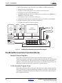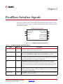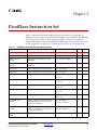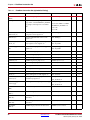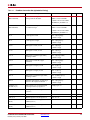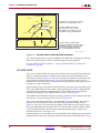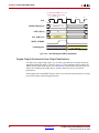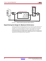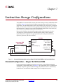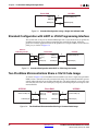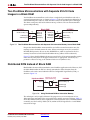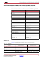
1
PicoBlaze 8-bit
Embedded Microcontroller
User Guide
for Spartan-3, Spartan-6, Virtex-5,
and Virtex-6 FPGAs
UG129 (v2.0) January 28, 2010
R
Xilinx is disclosing this Document and Intellectual Property (hereinafter “the Design”) to you for use in the development of designs to operate
on, or interface with Xilinx FPGAs. Except as stated herein, none of the Design may be copied, reproduced, distributed, republished,
downloaded, displayed, posted, or transmitted in any form or by any means including, but not limited to, electronic, mechanical,
photocopying, recording, or otherwise, without the prior written consent of Xilinx. Any unauthorized use of the Design may violate copyright
laws, trademark laws, the laws of privacy and publicity, and communications regulations and statutes.
Xilinx does not assume any liability arising out of the application or use of the Design; nor does Xilinx convey any license under its patents,
copyrights, or any rights of others. You are responsible for obtaining any rights you may require for your use or implementation of the Design.
Xilinx reserves the right to make changes, at any time, to the Design as deemed desirable in the sole discretion of Xilinx. Xilinx assumes no
obligation to correct any errors contained herein or to advise you of any correction if such be made. Xilinx will not assume any liability for the
accuracy or correctness of any engineering or technical support or assistance provided to you in connection with the Design.
THE DESIGN IS PROVIDED “AS IS” WITH ALL FAULTS, AND THE ENTIRE RISK AS TO ITS FUNCTION AND IMPLEMENTATION IS
WITH YOU. YOU ACKNOWLEDGE AND AGREE THAT YOU HAVE NOT RELIED ON ANY ORAL OR WRITTEN INFORMATION OR
ADVICE, WHETHER GIVEN BY XILINX, OR ITS AGENTS OR EMPLOYEES. XILINX MAKES NO OTHER WARRANTIES, WHETHER
EXPRESS, IMPLIED, OR STATUTORY, REGARDING THE DESIGN, INCLUDING ANY WARRANTIES OF MERCHANTABILITY, FITNESS
FOR A PARTICULAR PURPOSE, TITLE, AND NONINFRINGEMENT OF THIRD-PARTY RIGHTS.
IN NO EVENT WILL XILINX BE LIABLE FOR ANY CONSEQUENTIAL, INDIRECT, EXEMPLARY, SPECIAL, OR INCIDENTAL DAMAGES,
INCLUDING ANY LOST DATA AND LOST PROFITS, ARISING FROM OR RELATING TO YOUR USE OF THE DESIGN, EVEN IF YOU
HAVE BEEN ADVISED OF THE POSSIBILITY OF SUCH DAMAGES. THE TOTAL CUMULATIVE LIABILITY OF XILINX IN CONNECTION
WITH YOUR USE OF THE DESIGN, WHETHER IN CONTRACT OR TORT OR OTHERWISE, WILL IN NO EVENT EXCEED THE
AMOUNT OF FEES PAID BY YOU TO XILINX HEREUNDER FOR USE OF THE DESIGN. YOU ACKNOWLEDGE THAT THE FEES, IF
ANY, REFLECT THE ALLOCATION OF RISK SET FORTH IN THIS AGREEMENT cc THAT XILINX WOULD NOT MAKE AVAILABLE THE
DESIGN TO YOU WITHOUT THESE LIMITATIONS OF LIABILITY.
The Design is not designed or intended for use in the development of on-line control equipment in hazardous environments requiring failsafe controls, such as in the operation of nuclear facilities, aircraft navigation or communications systems, air traffic control, life support, or
weapons systems (“High-Risk Applications”). Xilinx specifically disclaims any express or implied warranties of fitness for such High-Risk
Applications. You represent that use of the Design in such High-Risk Applications is fully at your risk.
© 2004-2008 Xilinx, Inc. All rights reserved. XILINX, the Xilinx logo, and other designated brands included herein are trademarks of Xilinx,
Inc. PowerPC is a trademark of IBM Corp. and used under license. PCI, PCI-X, and PCI EXPRESS are registered trademarks of PCI-SIG.
All other trademarks are the property of their respective owners.
Revision History
The following table shows the revision history for this document...
Version
Revision
05/20/04
1.0
Initial Xilinx release.
06/10/04
1.1
Various minor corrections, updates, and enhancements throughout.
11/21/05
1.1.1
Minor updates.
06/24/08
1.1.2
Corrected typo in example for “LOAD sX, Operand — Load Register sX with Operand”.
Updated trademarks and links.
10/09/09
1.1.3
Added Spartan-6, Virtex-5, and Virtex-6 FPGA callouts in Title page.
1/28/10
2.0
Updated to v2.0; removed references to Virtex-II; clarified device family optimization;
converted to current user guide template.
PicoBlaze 8-bit Embedded Processor
www.xilinx.com
UG129 (v2.0) January 28, 2010
Preface
Limitations
Limited Warranty and Disclaimer
These designs are provided to you “as-is”. Xilinx and its licensors make and you receive no
warranties or conditions, express, implied, statutory or otherwise, and Xilinx specifically
disclaims any implied warranties of merchantability, non-infringement, or fitness for a
particular purpose. Xilinx does not warrant that the functions contained in these designs
will meet your requirements, or that the operation of these designs will be uninterrupted
or error free, or that defects in the Designs will be corrected. Furthermore, Xilinx does not
warrant or make any representations regarding use or the results of the use of the designs
in terms of correctness, accuracy, reliability, or otherwise.
Limitation of Liability
In no event will Xilinx or its licensors be liable for any loss of data, lost profits, cost or
procurement of substitute goods or services, or for any special, incidental, consequential,
or indirect damages arising from the use or operation of the designs or accompanying
documentation, however caused and on any theory of liability. This limitation will apply
even if Xilinx has been advised of the possibility of such damage. This limitation shall
apply not-withstanding the failure of the essential purpose of any limited remedies herein.
Technical Support Limitations
This module is not supported by general Xilinx Technical support as an official Xilinx
product. Please refer any issues initially to the provider of the module. The author will
gratefully receive any issues or potential continued improvements of the PicoBlaze™
microcontroller.
Ken Chapman
Senior Staff Engineer
E-mail: [email protected]
The author will also be pleased to hear from anyone using the PicoBlaze™ microcontroller
with information about your application and how these macros have been useful.
PicoBlaze 8-bit Embedded Microprocessor
UG129 (v2.0) January 28, 2010
www.xilinx.com
3
Preface: Acknowledgments
Acknowledgments
Xilinx thanks the following individuals for their contribution to the PicoBlaze
microcontroller cause:
4
•
Henk van Kampen, Mediatronix
Developer of the pBlazIDE graphical, integrated development environment.
•
Prof. Dr.-Ing. Bernhard Lang, University of Applied Sciences, Osrabrueck,
Germany
Concept of using VHDL simulation variables to display disassembled op-code
instructions.
•
Kris Chaplin, Xilinx Ltd.
JTAG-based program loader, update function.
www.xilinx.com
PicoBlaze 8-bit Embedded Microprocessor
UG129 (v2.0) January 28, 2010
Guide Contents
About This Guide
The PicoBlaze™ embedded microcontroller is an efficient, cost-effective embedded
processor core for Spartan®-3, Spartan-6, Virtex®-5, and Virtex-6 FPGAs. This user guide
describes the capabilities, features, and benefits of PicoBlaze hardware design and how to
effectively use the PicoBlaze instruction set and tools to create software applications.
Guide Contents
This manual contains the following chapters:
•
Chapter 1, “Introduction,” describes the features and functional blocks of the
PicoBlaze microcontroller.
•
Chapter 2, “PicoBlaze Interface Signals,” defines the PicoBlaze signals.
•
Chapter 3, “PicoBlaze Instruction Set,” summarizes the instruction set of the
PicoBlaze microcontrollers.
•
Chapter 4, “Interrupts,” describes how the PicoBlaze microcontroller uses interrupts.
•
Chapter 5, “Scratchpad RAM,” describes the 64-byte scratchpad RAM.
•
Chapter 6, “Input and Output Ports,” describes the input and output ports supported
by the PicoBlaze microcontroller.
•
Chapter 7, “Instruction Storage Configurations,” provides several examples of
instruction storage with the PicoBlaze microcontroller.
•
Chapter 8, “Performance,”provides performance values for the PicoBlaze
microcontroller.
•
Chapter 9, “Using the PicoBlaze Microcontroller in an FPGA Design,” describes the
design flow process with the PicoBlaze microcontroller.
•
Chapter 10, “PicoBlaze Development Tools,” describes the available development
tools.
•
Chapter 11, “Assembler Directives,” describes the assembler directives that provide
advanced control.
•
Chapter 12, “Simulating PicoBlaze Code,” describes the tools that simulate PicoBlaze
code.
•
Appendix A, “Related Materials and References,” provides additional resources
useful for the PicoBlaze microcontroller design.
•
Appendix B, “Example Program Templates,” provides example KCPSM3 and
pBlazIDE code templates for use in application programs.
•
Appendix C, “PicoBlaze Instruction Set and Event Reference,” summarizes the
PicoBlaze instructions and events in alphabetical order.
•
Appendix D, “Instruction Codes,” provides the 18-bit instruction codes for all
PicoBlaze instructions.
•
Appendix E, “Register and Scratchpad RAM Planning Worksheets,” provides
worksheets to use for the PicoBlaze microcontroller design.
PicoBlaze 8-bit Embedded Microprocessor
UG129 (v2.0) January 28, 2010
www.xilinx.com
5
Preface: About This Guide
6
www.xilinx.com
PicoBlaze 8-bit Embedded Microprocessor
UG129 (v2.0) January 28, 2010
Table of Contents
Preface: Limitations
Limited Warranty and Disclaimer . . . . . . . . . . . . . . . . . . . . . . . . . . . . . . . . . . . . . . . . . . . . 3
Limitation of Liability . . . . . . . . . . . . . . . . . . . . . . . . . . . . . . . . . . . . . . . . . . . . . . . . . . . . . . . . 3
Technical Support Limitations . . . . . . . . . . . . . . . . . . . . . . . . . . . . . . . . . . . . . . . . . . . . . . . 3
Preface: Acknowledgments
About This Guide
Guide Contents . . . . . . . . . . . . . . . . . . . . . . . . . . . . . . . . . . . . . . . . . . . . . . . . . . . . . . . . . . . . . . 5
Chapter 1: Introduction
PicoBlaze Microcontroller Features . . . . . . . . . . . . . . . . . . . . . . . . . . . . . . . . . . . . . . . . . . 13
PicoBlaze Microcontroller Functional Blocks . . . . . . . . . . . . . . . . . . . . . . . . . . . . . . . . 14
General-Purpose Registers . . . . . . . . . . . . . . . . . . . . . . . . . . . . . . . . . . . . . . . . . . . . . . . . .
1,024-Instruction Program Store . . . . . . . . . . . . . . . . . . . . . . . . . . . . . . . . . . . . . . . . . . . .
Arithmetic Logic Unit (ALU) . . . . . . . . . . . . . . . . . . . . . . . . . . . . . . . . . . . . . . . . . . . . . . .
Flags . . . . . . . . . . . . . . . . . . . . . . . . . . . . . . . . . . . . . . . . . . . . . . . . . . . . . . . . . . . . . . . . . . . .
64-Byte Scratchpad RAM . . . . . . . . . . . . . . . . . . . . . . . . . . . . . . . . . . . . . . . . . . . . . . . . . .
Input/Output . . . . . . . . . . . . . . . . . . . . . . . . . . . . . . . . . . . . . . . . . . . . . . . . . . . . . . . . . . . .
Program Counter (PC). . . . . . . . . . . . . . . . . . . . . . . . . . . . . . . . . . . . . . . . . . . . . . . . . . . . .
Program Flow Control. . . . . . . . . . . . . . . . . . . . . . . . . . . . . . . . . . . . . . . . . . . . . . . . . . . . .
CALL/RETURN Stack . . . . . . . . . . . . . . . . . . . . . . . . . . . . . . . . . . . . . . . . . . . . . . . . . . . .
Interrupts . . . . . . . . . . . . . . . . . . . . . . . . . . . . . . . . . . . . . . . . . . . . . . . . . . . . . . . . . . . . . . . .
Reset . . . . . . . . . . . . . . . . . . . . . . . . . . . . . . . . . . . . . . . . . . . . . . . . . . . . . . . . . . . . . . . . . . . .
14
14
15
15
15
15
16
16
16
16
16
Why the PicoBlaze Microcontroller? . . . . . . . . . . . . . . . . . . . . . . . . . . . . . . . . . . . . . . . . . 17
Why Use a Microcontroller within an FPGA? . . . . . . . . . . . . . . . . . . . . . . . . . . . . . . . . 17
Chapter 2: PicoBlaze Interface Signals
Chapter 3: PicoBlaze Instruction Set
Address Spaces . . . . . . . . . . . . . . . . . . . . . . . . . . . . . . . . . . . . . . . . . . . . . . . . . . . . . . . . . . . . . 24
Processing Data . . . . . . . . . . . . . . . . . . . . . . . . . . . . . . . . . . . . . . . . . . . . . . . . . . . . . . . . . . . . . 26
Logic Instructions . . . . . . . . . . . . . . . . . . . . . . . . . . . . . . . . . . . . . . . . . . . . . . . . . . . . . . . . .
Bitwise AND, OR, XOR . . . . . . . . . . . . . . . . . . . . . . . . . . . . . . . . . . . . . . . . . . . . . . . . .
Complement/Invert Register . . . . . . . . . . . . . . . . . . . . . . . . . . . . . . . . . . . . . . . . . . . . .
Invert or Toggle Bit . . . . . . . . . . . . . . . . . . . . . . . . . . . . . . . . . . . . . . . . . . . . . . . . . . . . .
Clear Register . . . . . . . . . . . . . . . . . . . . . . . . . . . . . . . . . . . . . . . . . . . . . . . . . . . . . . . . .
Set Bit . . . . . . . . . . . . . . . . . . . . . . . . . . . . . . . . . . . . . . . . . . . . . . . . . . . . . . . . . . . . . . .
Clear Bit . . . . . . . . . . . . . . . . . . . . . . . . . . . . . . . . . . . . . . . . . . . . . . . . . . . . . . . . . . . . .
Arithmetic Instructions . . . . . . . . . . . . . . . . . . . . . . . . . . . . . . . . . . . . . . . . . . . . . . . . . . . .
ADD and ADDCY Add Instructions. . . . . . . . . . . . . . . . . . . . . . . . . . . . . . . . . . . . . . . .
SUB and SUBCY Subtract Instructions . . . . . . . . . . . . . . . . . . . . . . . . . . . . . . . . . . . . . .
PicoBlaze 8-bit Embedded Microcontroller
UG129 (v2.0) January 28, 2010
www.xilinx.com
26
26
27
27
27
27
28
28
28
29
7
Increment/Decrement . . . . . . . . . . . . . . . . . . . . . . . . . . . . . . . . . . . . . . . . . . . . . . . . . . 29
Negate . . . . . . . . . . . . . . . . . . . . . . . . . . . . . . . . . . . . . . . . . . . . . . . . . . . . . . . . . . . . . . . 30
Multiplication . . . . . . . . . . . . . . . . . . . . . . . . . . . . . . . . . . . . . . . . . . . . . . . . . . . . . . . . . . . .
Division . . . . . . . . . . . . . . . . . . . . . . . . . . . . . . . . . . . . . . . . . . . . . . . . . . . . . . . . . . . . . . . . .
No Operation (NOP) . . . . . . . . . . . . . . . . . . . . . . . . . . . . . . . . . . . . . . . . . . . . . . . . . . . . . .
Setting and Clearing CARRY Flag . . . . . . . . . . . . . . . . . . . . . . . . . . . . . . . . . . . . . . . . . . .
Clear CARRY Flag . . . . . . . . . . . . . . . . . . . . . . . . . . . . . . . . . . . . . . . . . . . . . . . . . . . . .
Set CARRY Flag . . . . . . . . . . . . . . . . . . . . . . . . . . . . . . . . . . . . . . . . . . . . . . . . . . . . . . .
Test and Compare . . . . . . . . . . . . . . . . . . . . . . . . . . . . . . . . . . . . . . . . . . . . . . . . . . . . . . . .
Test . . . . . . . . . . . . . . . . . . . . . . . . . . . . . . . . . . . . . . . . . . . . . . . . . . . . . . . . . . . . . . . . .
Compare . . . . . . . . . . . . . . . . . . . . . . . . . . . . . . . . . . . . . . . . . . . . . . . . . . . . . . . . . . . . .
Shift and Rotate Instructions . . . . . . . . . . . . . . . . . . . . . . . . . . . . . . . . . . . . . . . . . . . . . . .
Shift . . . . . . . . . . . . . . . . . . . . . . . . . . . . . . . . . . . . . . . . . . . . . . . . . . . . . . . . . . . . . . . . .
Rotate . . . . . . . . . . . . . . . . . . . . . . . . . . . . . . . . . . . . . . . . . . . . . . . . . . . . . . . . . . . . . . .
30
32
33
34
34
34
34
34
36
36
36
37
Moving Data . . . . . . . . . . . . . . . . . . . . . . . . . . . . . . . . . . . . . . . . . . . . . . . . . . . . . . . . . . . . . . . . 38
Program Flow Control . . . . . . . . . . . . . . . . . . . . . . . . . . . . . . . . . . . . . . . . . . . . . . . . . . . . . . . 38
JUMP . . . . . . . . . . . . . . . . . . . . . . . . . . . . . . . . . . . . . . . . . . . . . . . . . . . . . . . . . . . . . . . . . . . 39
CALL/RETURN . . . . . . . . . . . . . . . . . . . . . . . . . . . . . . . . . . . . . . . . . . . . . . . . . . . . . . . . . . 40
Chapter 4: Interrupts
Example Interrupt Flow . . . . . . . . . . . . . . . . . . . . . . . . . . . . . . . . . . . . . . . . . . . . . . . . . . . . . 44
Chapter 5: Scratchpad RAM
Address Modes . . . . . . . . . . . . . . . . . . . . . . . . . . . . . . . . . . . . . . . . . . . . . . . . . . . . . . . . . . . . . 47
Direct Addressing . . . . . . . . . . . . . . . . . . . . . . . . . . . . . . . . . . . . . . . . . . . . . . . . . . . . . . . . 47
Indirect Addressing . . . . . . . . . . . . . . . . . . . . . . . . . . . . . . . . . . . . . . . . . . . . . . . . . . . . . . . 47
Implementing a Look-Up Table . . . . . . . . . . . . . . . . . . . . . . . . . . . . . . . . . . . . . . . . . . . . . 48
Stack Operations . . . . . . . . . . . . . . . . . . . . . . . . . . . . . . . . . . . . . . . . . . . . . . . . . . . . . . . . . . . . 49
FIFO Operations . . . . . . . . . . . . . . . . . . . . . . . . . . . . . . . . . . . . . . . . . . . . . . . . . . . . . . . . . . . . 49
Chapter 6: Input and Output Ports
PORT_ID Port . . . . . . . . . . . . . . . . . . . . . . . . . . . . . . . . . . . . . . . . . . . . . . . . . . . . . . . . . . . . . . 51
INPUT Operations . . . . . . . . . . . . . . . . . . . . . . . . . . . . . . . . . . . . . . . . . . . . . . . . . . . . . . . . . . 52
Applications with Few Input Sources . . . . . . . . . . . . . . . . . . . . . . . . . . . . . . . . . . . . . . . . 54
READ_STROBE Interaction with FIFOs . . . . . . . . . . . . . . . . . . . . . . . . . . . . . . . . . . . . . . 54
OUTPUT Operations . . . . . . . . . . . . . . . . . . . . . . . . . . . . . . . . . . . . . . . . . . . . . . . . . . . . . . . . 55
Simple Output Structure for Few Output Destinations . . . . . . . . . . . . . . . . . . . . . . . . . 56
Pipelining for Maximum Performance . . . . . . . . . . . . . . . . . . . . . . . . . . . . . . . . . . . . . . . 58
Repartitioning the Design for Maximum Performance . . . . . . . . . . . . . . . . . . . . . . . 60
Chapter 7: Instruction Storage Configurations
Standard Configuration – Single 1Kx18 Block RAM . . . . . . . . . . . . . . . . . . . . . . . . .
Standard Configuration with UART or JTAG Programming Interface . . . . . . . .
Two PicoBlaze Microcontrollers Share a 1Kx18 Code Image . . . . . . . . . . . . . . . . . .
Two PicoBlaze Microcontrollers with Separate Code Images in a Block RAM
Distributed ROM Instead of Block RAM . . . . . . . . . . . . . . . . . . . . . . . . . . . . . . . . . . . .
8
www.xilinx.com
61
62
62
63
63
PicoBlaze 8-bit Embedded Microcontroller
UG129 (v2.0) January 28, 2010
Chapter 8: Performance
Input Clock Frequency . . . . . . . . . . . . . . . . . . . . . . . . . . . . . . . . . . . . . . . . . . . . . . . . . . . . . . 65
Predicting Executing Performance . . . . . . . . . . . . . . . . . . . . . . . . . . . . . . . . . . . . . . . . . . . 65
Chapter 9: PicoBlaze Development Tools
KCPSM3 . . . . . . . . . . . . . . . . . . . . . . . . . . . . . . . . . . . . . . . . . . . . . . . . . . . . . . . . . . . . . . . . . . . . 67
Assembler . . . . . . . . . . . . . . . . . . . . . . . . . . . . . . . . . . . . . . . . . . . . . . . . . . . . . . . . . . . . . . . 67
Assembly Errors . . . . . . . . . . . . . . . . . . . . . . . . . . . . . . . . . . . . . . . . . . . . . . . . . . . . . . . . . . 68
Input and Output Files . . . . . . . . . . . . . . . . . . . . . . . . . . . . . . . . . . . . . . . . . . . . . . . . . . . . 68
Mediatronix pBlazIDE . . . . . . . . . . . . . . . . . . . . . . . . . . . . . . . . . . . . . . . . . . . . . . . . . . . . . . 69
Configuring pBlazIDE for the PicoBlaze Microcontroller . . . . . . . . . . . . . . . . . . . . . . . 69
Importing KCPSM3 Code into pBlazIDE . . . . . . . . . . . . . . . . . . . . . . . . . . . . . . . . . . . . . 70
Differences Between the KCPSM3 Assembler and pBlazIDE . . . . . . . . . . . . . . . . . 71
Directives . . . . . . . . . . . . . . . . . . . . . . . . . . . . . . . . . . . . . . . . . . . . . . . . . . . . . . . . . . . . . . . . . . . 71
Chapter 10: Using the PicoBlaze Microcontroller in an FPGA Design
VHDL Design Flow . . . . . . . . . . . . . . . . . . . . . . . . . . . . . . . . . . . . . . . . . . . . . . . . . . . . . . . . . 73
KCPSM3 Module . . . . . . . . . . . . . . . . . . . . . . . . . . . . . . . . . . . . . . . . . . . . . . . . . . . . . . . . . 73
Connecting the Program ROM . . . . . . . . . . . . . . . . . . . . . . . . . . . . . . . . . . . . . . . . . . . . . 74
Black Box Instantiation of KCPSM3 using KCPSM3.ngc . . . . . . . . . . . . . . . . . . . . . 75
Generating the Program ROM using prog_rom.coe . . . . . . . . . . . . . . . . . . . . . . . . . . . . 75
Generating an ESC Schematic Symbol . . . . . . . . . . . . . . . . . . . . . . . . . . . . . . . . . . . . . . . 75
Verilog Design Flow . . . . . . . . . . . . . . . . . . . . . . . . . . . . . . . . . . . . . . . . . . . . . . . . . . . . . . . . 75
Chapter 11: Assembler Directives
Locating Code at a Specific Address . . . . . . . . . . . . . . . . . . . . . . . . . . . . . . . . . . . . . . . . .
Naming or Aliasing Registers . . . . . . . . . . . . . . . . . . . . . . . . . . . . . . . . . . . . . . . . . . . . . . .
Defining Constants . . . . . . . . . . . . . . . . . . . . . . . . . . . . . . . . . . . . . . . . . . . . . . . . . . . . . . . . .
Naming the Program ROM Output File . . . . . . . . . . . . . . . . . . . . . . . . . . . . . . . . . . . . . .
77
77
78
78
KCPSM3 . . . . . . . . . . . . . . . . . . . . . . . . . . . . . . . . . . . . . . . . . . . . . . . . . . . . . . . . . . . . . . . . 78
pBlazIDE . . . . . . . . . . . . . . . . . . . . . . . . . . . . . . . . . . . . . . . . . . . . . . . . . . . . . . . . . . . . . . . . 78
Defining I/O Ports (pBlazIDE) . . . . . . . . . . . . . . . . . . . . . . . . . . . . . . . . . . . . . . . . . . . . . . . 78
Input Ports . . . . . . . . . . . . . . . . . . . . . . . . . . . . . . . . . . . . . . . . . . . . . . . . . . . . . . . . . . . . . . . 79
Output Ports . . . . . . . . . . . . . . . . . . . . . . . . . . . . . . . . . . . . . . . . . . . . . . . . . . . . . . . . . . . . . 79
Input/Output Ports . . . . . . . . . . . . . . . . . . . . . . . . . . . . . . . . . . . . . . . . . . . . . . . . . . . . . . . 80
Custom Instruction Op-Codes . . . . . . . . . . . . . . . . . . . . . . . . . . . . . . . . . . . . . . . . . . . . . . . 81
Chapter 12: Simulating PicoBlaze Code
Instruction Set Simulation with pBlazIDE . . . . . . . . . . . . . . . . . . . . . . . . . . . . . . . . . . . 84
Simulator Control Buttons . . . . . . . . . . . . . . . . . . . . . . . . . . . . . . . . . . . . . . . . . . . . . . . . . 85
Using the pBlazIDE Instruction Set Simulator with KCPSM3 Programs . . . . . . . . . . 86
Simulating FPGA Interaction with the pBlazIDE Instruction Set Simulator . . . . . . . 86
Turbocharging Simulation using FPGAs! . . . . . . . . . . . . . . . . . . . . . . . . . . . . . . . . . . . . 87
PicoBlaze 8-bit Embedded Microcontroller
UG129 (v2.0) January 28, 2010
www.xilinx.com
9
Appendix A: Related Materials and References
Appendix B: Example Program Templates
KCPSM3 Syntax . . . . . . . . . . . . . . . . . . . . . . . . . . . . . . . . . . . . . . . . . . . . . . . . . . . . . . . . . . . . 91
pBlazIDE Syntax . . . . . . . . . . . . . . . . . . . . . . . . . . . . . . . . . . . . . . . . . . . . . . . . . . . . . . . . . . . . 92
Appendix C: PicoBlaze Instruction Set and Event Reference
ADD sX, Operand —Add Operand to Register sX . . . . . . . . . . . . . . . . . . . . . . . . . . . . 93
ADDCY sX, Operand —Add Operand to Register sX with Carry . . . . . . . . . . . . . 94
AND sX, Operand — Logical Bitwise AND Register sX with Operand. . . . . . . . 95
CALL [Condition,] Address — Call Subroutine at Specified Address . . . . . . . . . 96
COMPARE sX, Operand — Compare Operand with Register sX. . . . . . . . . . . . . . 98
DISABLE INTERRUPT — Disable External Interrupt Input . . . . . . . . . . . . . . . . . . 99
ENABLE INTERRUPT — Enable External Interrupt Input . . . . . . . . . . . . . . . . . . . 99
FETCH sX, Operand — Read Scratchpad RAM Location to Register sX . . . . . . 100
INPUT sX, Operand — Set PORT_ID to Operand, Read value on IN_PORT . 101
INTERRUPT Event, When Enabled . . . . . . . . . . . . . . . . . . . . . . . . . . . . . . . . . . . . . . . . . 102
JUMP [Condition,] Address — Jump to Specified Address . . . . . . . . . . . . . . . . . . 103
LOAD sX, Operand — Load Register sX with Operand. . . . . . . . . . . . . . . . . . . . . . 104
OR sX, Operand — Logical Bitwise OR Register sX with Operand . . . . . . . . . . 105
OUTPUT sX, Operand — Write Register sX Value to OUT_PORT . . . . . . . . . . . 106
RESET Event . . . . . . . . . . . . . . . . . . . . . . . . . . . . . . . . . . . . . . . . . . . . . . . . . . . . . . . . . . . . . . . 107
RETURN [Condition] — Return from Subroutine Call . . . . . . . . . . . . . . . . . . . . . . 108
RETURNI [ENABLE/DISABLE] — Return from Interrupt Service Routine . . 109
RL sX — Rotate Left Register sX . . . . . . . . . . . . . . . . . . . . . . . . . . . . . . . . . . . . . . . . . . . . 110
RR sX — Rotate Right Register sX . . . . . . . . . . . . . . . . . . . . . . . . . . . . . . . . . . . . . . . . . . 110
SL[ 0 | 1 | X | A ] sX — Shift Left Register sX . . . . . . . . . . . . . . . . . . . . . . . . . . . . . . 111
SR[ 0 | 1 | X | A ] sX — Shift Right Register sX . . . . . . . . . . . . . . . . . . . . . . . . . . . . . 112
STORE sX, Operand — Write Register sX Value to Scratchpad RAM . . . . . . . . 114
SUB sX, Operand —Subtract Operand from Register sX . . . . . . . . . . . . . . . . . . . . . 115
SUBCY sX, Operand —Subtract Operand from Register sX with Borrow . . . . 116
TEST sX, Operand — Test Bit Location in Register sX, Generate Odd Parity . 118
XOR sX, Operand — Logical Bitwise XOR Register sX with Operand. . . . . . . . 120
Appendix D: Instruction Codes
Appendix E: Register and Scratchpad RAM Planning Worksheets
Registers . . . . . . . . . . . . . . . . . . . . . . . . . . . . . . . . . . . . . . . . . . . . . . . . . . . . . . . . . . . . . . . . . . . 125
Scratchpad RAM . . . . . . . . . . . . . . . . . . . . . . . . . . . . . . . . . . . . . . . . . . . . . . . . . . . . . . . . . . . 126
10
www.xilinx.com
PicoBlaze 8-bit Embedded Microcontroller
UG129 (v2.0) January 28, 2010
Chapter 1
Introduction
The PicoBlaze™ microcontroller is a compact, capable, and cost-effective fully embedded
8-bit RISC microcontroller core optimized for the Spartan®-3 family, with support for the
Virtex®-5, Spartan-6, and Virtex®-6 FPGA families. The PicoBlaze microcontroller provides
cost-efficient microcontroller-based control and simple data processing.
The PicoBlaze microcontroller is optimized for efficiency and low deployment cost. It
occupies just 96 FPGA slices, or only 12.5% of an XC3S50 FPGA and a miniscule 0.3% of an
XC3S5000 FPGA. In typical implementations, a single FPGA block RAM stores up to 1024
program instructions, which are automatically loaded during FPGA configuration. Even
with such resource efficiency, the PicoBlaze microcontroller performs a respectable 44 to
100 million instructions per second (MIPS) depending on the target FPGA family and
speed grade.
The PicoBlaze microcontroller core is totally embedded within the target FPGA and
requires no external resources. The PicoBlaze microcontroller is extremely flexible. The
basic functionality is easily extended and enhanced by connecting additional FPGA logic
to the microcontroller’s input and output ports.
The PicoBlaze microcontroller provides abundant, flexible I/O at much lower cost than
off-the-shelf controllers. Similarly, the PicoBlaze peripheral set can be customized to meet
the specific features, function, and cost requirements of the target application. Because the
PicoBlaze microcontroller is delivered as synthesizable VHDL source code, the core is
future-proof and can be migrated to future FPGA architectures, effectively eliminating
product obsolescence fears. Being integrated within the FPGA, the PicoBlaze
microcontroller reduces board space, design cost, and inventory.
The PicoBlaze FPC is supported by a suite of development tools including an assembler, a
graphical integrated development environment (IDE), a graphical instruction set
simulator, and VHDL source code and simulation models. Similarly, the PicoBlaze
microcontroller is also supported in the Xilinx System Generator development
environment.
The various PicoBlaze code examples throughout this application note are written for the
Xilinx KCPSM3 assembler. The Mediatronix pBlazIDE assembler has a code import
function that reads the KCPSM3 syntax.
PicoBlaze Microcontroller Features
As shown in the block diagram in Figure 1-1, the PicoBlaze microcontroller supports the
following features:
•
16 byte-wide general-purpose data registers
•
1K instructions of programmable on-chip program store, automatically loaded during
FPGA configuration
PicoBlaze 8-bit Embedded Microcontroller
UG129 (v2.0) January 28, 2010
www.xilinx.com
11
Chapter 1: Introduction
•
64-byte internal scratchpad RAM
•
256 input and 256 output ports for easy expansion and enhancement
•
Automatic 31-location CALL/RETURN stack
•
Predictable performance, always two clock cycles per instruction, up to 200 MHz or
100 MIPS in a Virtex-II Pro FPGA
•
Fast interrupt response; worst-case 5 clock cycles
•
Optimized for Xilinx Spartan-3 architecture—just 96 slices and 0.5 to 1 block RAM
•
Support in Spartan-6, and Virtex-6 FPGA architectures
•
Assembler, instruction-set simulator support
31x10
CALL/RETURN
Stack
Byte-wide Arithmetic Logic Unit (ALU) with CARRY and ZERO indicator flags
Program Counter
(PC)
1Kx18
Instruction
PROM
•
PORT_ID
64-Byte
Scratchpad RAM
OUT_PORT
Flags
Instruction
Decoder
Constants
INTERRUPT
IE
16 Byte-Wide Registers
Enable
s0
s4
s8
sC
IN_PORT
s1
s5
s9
sD
s2
s6
sA
sE
Operand 1
s3
s7
sB
sF
Z
Zero
C
Carry
ALU
Operand 2
UG129_c1_01_051204
Figure 1-1:
PicoBlaze Embedded Microcontroller Block Diagram
PicoBlaze Microcontroller Functional Blocks
General-Purpose Registers
The PicoBlaze microcontroller includes 16 byte-wide general-purpose registers,
designated as registers s0 through sF. For better program clarity, registers can be renamed
using an assembler directive. All register operations are completely interchangeable; no
registers are reserved for special tasks or have priority over any other register. There is no
dedicated accumulator; each result is computed in a specified register.
1,024-Instruction Program Store
The PicoBlaze microcontroller executes up to 1,024 instructions from memory within the
FPGA, typically from a single block RAM. Each PicoBlaze instruction is 18 bits wide. The
instructions are compiled within the FPGA design and automatically loaded during the
FPGA configuration process.
12
www.xilinx.com
PicoBlaze 8-bit Embedded Microcontroller
UG129 (v2.0) January 28, 2010
PicoBlaze Microcontroller Functional Blocks
Other memory organizations are possible to accommodate more PicoBlaze controllers
within a single FPGA or to enable interactive code updates without recompiling the FPGA
design. See Chapter 7, “Instruction Storage Configurations,” for more information.
Arithmetic Logic Unit (ALU)
The byte-wide Arithmetic Logic Unit (ALU) performs all microcontroller calculations,
including:
•
basic arithmetic operations such as addition and subtraction
•
bitwise logic operations such as AND, OR, and XOR
•
arithmetic compare and bitwise test operations
•
comprehensive shift and rotate operations
All operations are performed using an operand provided by any specified register (sX).
The result is returned to the same specified register (sX). If an instruction requires a second
operand, then the second operand is either a second register (sY) or an 8-bit immediate
constant (kk).
Flags
ALU operations affect the ZERO and CARRY flags. The ZERO flag indicates when the
result of the last operation resulted in zero. The CARRY flag indicates various conditions,
depending on the last instruction executed.
The INTERRUPT_ENABLE flag enables the INTERRUPT input.
64-Byte Scratchpad RAM
The PicoBlaze microcontroller provides an internal general-purpose 64-byte scratchpad
RAM, directly or indirectly addressable from the register file using the STORE and FETCH
instructions.
The STORE instruction writes the contents of any of the 16 registers to any of the 64 RAM
locations. The complementary FETCH instruction reads any of the 64 memory locations
into any of the 16 registers. This allows a much greater number of variables to be held
within the boundary of the processor and tends to reserve all of the I/O space for real
inputs and output signals.
The six-bit scratchpad RAM address is specified either directly (ss) with an immediate
constant, or indirectly using the contents of any of the 16 registers (sY). Only the lower six
bits of the address are used; the address should not exceed the 00 - 3F range of the available
memory.
Input/Output
The Input/Output ports extend the PicoBlaze microcontroller’s capabilities and allow the
microcontroller to connect to a custom peripheral set or to other FPGA logic. The PicoBlaze
microcontroller supports up to 256 input ports and 256 output ports or a combination of
input/output ports. The PORT_ID output provides the port address. During an INPUT
operation, the PicoBlaze microcontroller reads data from the IN_PORT port to a specified
register, sX. During an OUTPUT operation, the PicoBlaze microcontroller writes the
contents of a specified register, sX, to the OUT_PORT port.
See Chapter 6, “Input and Output Ports,” for more information.
PicoBlaze 8-bit Embedded Microcontroller
UG129 (v2.0) January 28, 2010
www.xilinx.com
13
Chapter 1: Introduction
Program Counter (PC)
The Program Counter (PC) points to the next instruction to be executed. By default, the PC
automatically increments to the next instruction location when executing an instruction.
Only the JUMP, CALL, RETURN, and RETURNI instructions and the Interrupt and Reset
Events modify the default behavior. The PC cannot be directly modified by the application
code; computed jump instructions are not supported.
The 10-bit PC supports a maximum code space of 1,024 instructions (000 to 3FF hex). If the
PC reaches the top of the memory at 3FF hex, it rolls over to location 000.
Program Flow Control
The default execution sequence of the program can be modified using conditional and
non-conditional program flow control instructions.
The JUMP instructions specify an absolute address anywhere in the 1,024-instruction
program space.
CALL and RETURN instructions provide subroutine facilities for commonly used sections of
code. A CALL instruction specifies the absolute start address of a subroutine, while the
return address is automatically preserved on the CALL/RETURN stack.
If the interrupt input is enabled, an Interrupt Event also preserves the address of the
preempted instruction on the CALL/RETURN stack while the PC is loaded with the
interrupt vector, 3FF hex. Use the RETURNI instruction instead of the RETURN instruction
to return from the interrupt service routine (ISR).
CALL/RETURN Stack
The CALL/RETURN hardware stack stores up to 31 instruction addresses, enabling
nested CALL sequences up to 31 levels deep. Since the stack is also used during an
interrupt operation, at least one of these levels should be reserved when interrupts are
enabled.
The stack is implemented as a separate cyclic buffer. When the stack is full, it overwrites
the oldest value. Consequently, there are no instructions to control the stack or the stack
pointer. No program memory is required for the stack.
Interrupts
The PicoBlaze microcontroller has an optional INTERRUPT input, allowing the PicoBlaze
microcontroller to handle asynchronous external events. In this context, “asynchronous”
relates to interrupts occurring at any time during an instruction cycle. However,
recommended design practice is to synchronize all inputs to the PicoBlaze controller using
the clock input.
The PicoBlaze microcontroller responds to interrupts quickly in just five clock cycles.
See Chapter 4, “Interrupts,” for more information.
Reset
The PicoBlaze microcontroller is automatically reset immediately after the FPGA
configuration process completes. After configuration, the RESET input forces the processor
into the initial state. The PC is reset to address 0, the flags are cleared, interrupts are
disabled, and the CALL/RETURN stack is reset.
14
www.xilinx.com
PicoBlaze 8-bit Embedded Microcontroller
UG129 (v2.0) January 28, 2010
Why the PicoBlaze Microcontroller?
The data registers and scratchpad RAM are not affected by Reset.
See “RESET Event” in Appendix C for more information.
Why the PicoBlaze Microcontroller?
There are literally dozens of 8-bit microcontroller architectures and instruction sets.
Modern FPGAs can efficiently implement practically any 8-bit microcontroller, and
available FPGA soft cores support popular instruction sets such as the PIC, 8051, AVR,
6502, 8080, and Z80 microcontrollers. Why use the PicoBlaze microcontroller instead of a
more popular instruction set?
The PicoBlaze microcontroller is specifically designed and optimized for the Spartan-3
family, and with support for Spartan-6, and Virtex-6 FPGA architectures. Its compact yet
capable architecture consumes considerably less FPGA resources than comparable 8-bit
microcontroller architectures within an FPGA. Furthermore, the PicoBlaze microcontroller
is provided as a free, source-level VHDL file with royalty-free re-use within Xilinx FPGAs.
Some standalone microcontroller variants have a notorious reputation for becoming
obsolete. Because it is delivered as VHDL source, the PicoBlaze microcontroller is immune
to product obsolescence as the microcontroller can be retargeted to future generations of
Xilinx FPGAs, exploiting future cost reductions and feature enhancements. Furthermore,
the PicoBlaze microcontroller is expandable and extendable.
Before the advent of the PicoBlaze and MicroBlaze™ embedded processors, the
microcontroller resided externally to the FPGA, limiting the connectivity to other FPGA
functions and restricting overall interface performance. By contrast, the PicoBlaze
microcontroller is fully embedded in the FPGA with flexible, extensive on-chip
connectivity to other FPGA resources. Signals remain within the FPGA, improving overall
performance. The PicoBlaze microcontroller reduces system cost because it is a single-chip
solution, integrated within the FPGA and sometimes only occupying leftover FPGA
resources.
The PicoBlaze microcontroller is resource efficient. Consequently, complex applications are
sometimes best portioned across multiple PicoBlaze microcontrollers with each controller
implementing a particular function, for example, keyboard and display control, or system
management.
Why Use a Microcontroller within an FPGA?
Microcontrollers and FPGAs both successfully implement practically any digital logic
function. However, each has unique advantages in cost, performance, and ease of use.
Microcontrollers are well suited to control applications, especially with widely changing
requirements. The FPGA resources required to implement the microcontroller are
relatively constant. The same FPGA logic is re-used by the various microcontroller
instructions, conserving resources. The program memory requirements grow with
increasing complexity.
Programming control sequences or state machines in assembly code is often easier than
creating similar structures in FPGA logic.
Microcontrollers are typically limited by performance. Each instruction executes
sequentially. As an application increases in complexity, the number of instructions
required to implement the application grows and system performance decreases
accordingly. By contrast, performance in an FPGA is more flexible. For example, an
algorithm can be implemented sequentially or completely in parallel, depending on the
PicoBlaze 8-bit Embedded Microcontroller
UG129 (v2.0) January 28, 2010
www.xilinx.com
15
Chapter 1: Introduction
performance requirements. A completely parallel implementation is faster but consumes
more FPGA resources.
A microcontroller embedded within the FPGA provides the best of both worlds. The
microcontroller implements non-timing crucial complex control functions while timingcritical or data path functions are best implemented using FPGA logic. For example, a
microcontroller cannot respond to events much faster than a few microseconds. The FPGA
logic can respond to multiple, simultaneous events in just a few to tens of nanoseconds.
Conversely, a microcontroller is cost-effective and simple for performing format or
protocol conversions.
Table 1-1: PicoBlaze Microcontroller Embedded within an FPGA Provides the Optimal Balance between
Microcontroller and FPGA Solutions
16
PicoBlaze Microcontroller
FPGA Logic
Strengths
• Easy to program, excellent for control and
state machine applications
• Resource requirements remain constant
with increasing complexity
• Re-uses logic resources, excellent for
lower-performance functions
• Significantly higher performance
• Excellent at parallel operations
• Sequential vs. parallel implementation tradeoffs optimize performance or cost
• Fast response to multiple, simultaneous inputs
Weaknesses
• Executes sequentially
• Performance degrades with increasing
complexity
• Program memory requirements increase
with increasing complexity
• Slower response to simultaneous inputs
• Control and state machine applications more
difficult to program
• Logic resources grow with increasing
complexity
www.xilinx.com
PicoBlaze 8-bit Embedded Microcontroller
UG129 (v2.0) January 28, 2010
Chapter 2
PicoBlaze Interface Signals
The top-level interface signals to the PicoBlaze microcontroller appear in Figure 2-1 and
are described in Table 2-1. Figure 7-1 provides additional detail on the internal structure of
the PicoBlaze controller.
PicoBlaze Microcontroller
IN_PORT[7:0]
INTERRUPT
RESET
OUT_PORT[7:0]
PORT_ID[7:0]
READ_STROBE
WRITE_STROBE
INTERRUPT_ACK
CLK
UG129_c2_01_052004
Figure 2-1:
Table 2-1:
PicoBlaze Interface Connections
PicoBlaze Interface Signal Descriptions
Signal
Direction
Description
IN_PORT[7:0]
Input
Input Data Port: Present valid input data on this port during an INPUT instruction.
The data is captured on the rising edge of CLK.
INTERRUPT
Input
Interrupt Input: If the INTERRUPT_ENABLE flag is set by the application code,
generate an INTERRUPT Event by asserting this input High for at least two CLK
cycles. If the INTERRUPT_ENABLE flag is cleared, this input is ignored.
RESET
Input
Reset Input: To reset the PicoBlaze microcontroller and to generate a RESET Event,
assert this input High for at least one CLK cycle. A Reset Event is automatically
generated immediately following FPGA configuration.
CLK
Input
Clock Input: The frequency may range from DC to the maximum operating
frequency reported by the Xilinx ISE® development software. All PicoBlaze
synchronous elements are clocked from the rising clock edge. There are no clock
duty-cycle requirements beyond the minimum pulse width requirements of the
FPGA.
OUT_PORT[7:0]
Output
Output Data Port: Output data appears on this port for two CLK cycles during an
OUTPUT instruction. Capture output data within the FPGA at the rising CLK edge
when WRITE_STROBE is High.
PORT_ID[7:0]
Output
Port Address: The I/O port address appears on this port for two CLK cycles during
an INPUT or OUTPUT instruction.
PicoBlaze 8-bit Embedded Microcontroller
UG129 (v2.0) January 28, 2010
www.xilinx.com
17
Chapter 2: PicoBlaze Interface Signals
Table 2-1:
PicoBlaze Interface Signal Descriptions (Cont’d)
Signal
Direction
Description
READ_STROBE
Output
Read Strobe: When asserted High, this signal indicates that input data on the
IN_PORT[7:0] port was captured to the specified data register during an INPUT
instruction. This signal is asserted on the second CLK cycle of the two-cycle INPUT
instruction. This signal is typically used to acknowledge read operations from
FIFOs.
WRITE_STROBE
Output
Write Strobe: When asserted High, this signal validates the output data on the
OUT_PORT[7:0] port during an OUTPUT instruction. This signal is asserted on the
second CLK cycle of the two-cycle OUTPUT instruction. Capture output data
within the FPGA on the rising CLK edge when WRITE_STROBE is High.
INTERRUPT_ACK
Output
Interrupt Acknowledge: When asserted High, this signal acknowledges that an
INTERRUPT Event occurred. This signal is asserted during the second CLK cycle
of the two-cycle INTERRUPT Event. This signal is optionally used to clear the
source of the INTERRUPT input.
18
www.xilinx.com
PicoBlaze 8-bit Embedded Microcontroller
UG129 (v2.0) January 28, 2010
Chapter 3
PicoBlaze Instruction Set
Table 3-1 summarizes the entire PicoBlaze processor instruction set, which appears
alphabetically. Instructions are listed using the KCPSM3 syntax. If different, the pBlazIDE
syntax appears in parentheses. Each instruction includes an overview description, a
functional description, and how the ZERO and CARRY flags are affected. For more details
on each instruction, see Appendix C, “PicoBlaze Instruction Set and Event Reference.”
Table 3-1:
PicoBlaze Instruction Set (alphabetical listing)
Instruction
Description
Function
ZERO
CARRY
ADD sX, kk
Add register sX with literal kk
sX Å sX + kk
?
?
ADD sX, sY
Add register sX with register sY
sX Å sX + sY
?
?
ADDCY sX, kk
(ADDC)
Add register sX with literal kk with
CARRY bit
sX Å sX + kk + CARRY
?
?
ADDCY sX, sY
(ADDC)
Add register sX with register sY with
CARRY bit
sX Å sX + sY + CARRY
?
?
AND sX, kk
Bitwise AND register sX with literal kk
sX Å sX AND kk
?
0
AND sX, sY
Bitwise AND register sX with register sY
sX Å sX AND sY
?
0
CALL aaa
Unconditionally call subroutine at aaa
TOS Å PC
-
-
PC Å aaa
CALL C, aaa
If CARRY flag set, call subroutine at aaa
If CARRY=1, {TOS Å PC,
PC Å aaa}
-
-
CALL NC, aaa
If CARRY flag not set, call subroutine at
aaa
If CARRY=0, {TOS Å PC,
PC Å aaa}
-
-
CALL NZ, aaa
If ZERO flag not set, call subroutine at aaa
If ZERO=0, {TOS Å PC,
PC Å aaa}
-
-
CALL Z, aaa
If ZERO flag set, call subroutine at aaa
If ZERO=1, {TOS Å PC,
PC Å aaa}
-
-
COMPARE sX, kk
(COMP)
Compare register sX with literal kk. Set
CARRY and ZERO flags as appropriate.
Registers are unaffected.
If sX=kk, ZERO Å 1
?
?
COMPARE sX, sY
(COMP)
Compare register sX with register sY. Set
CARRY and ZERO flags as appropriate.
Registers are unaffected.
If sX=sY, ZERO Å 1
?
?
DISABLE INTERRUPT
(DINT)
Disable interrupt input
INTERRUPT_ENABLE Å 0
-
-
PicoBlaze 8-bit Embedded Microcontroller
UG129 (v2.0) January 28, 2010
www.xilinx.com
If sX<kk, CARRY Å 1
If sX<sY, CARRY Å 1
19
Chapter 3: PicoBlaze Instruction Set
Table 3-1:
PicoBlaze Instruction Set (alphabetical listing)
Instruction
Description
Function
ZERO
CARRY
ENABLE INTERRUPT
(EINT)
Enable interrupt input
INTERRUPT_ENABLE Å 1
-
-
Interrupt Event
Asynchronous interrupt input. Preserve
flags and PC. Clear INTERRUPT_ENABLE
flag. Jump to interrupt vector at address
3FF.
Preserved ZERO Å ZERO
-
-
Preserved CARRY Å CARRY
INTERRUPT_ENABLE Å 0
TOS Å PC
PC Å 3FF
FETCH sX, (sY)
(FETCH sX, sY)
Read scratchpad RAM location pointed to
by register sY into register sX
sX Å RAM[(sY)]
-
-
FETCH sX, ss
Read scratchpad RAM location ss into
register sX
sX Å RAM[ss]
-
-
INPUT sX, (sY)
(IN sX, sY)
Read value on input port location pointed
to by register sY into register sX
PORT_ID Å sY
-
-
INPUT sX, pp
PORT_ID Å pp
-
-
(IN)
Read value on input port location pp into
register sX
JUMP aaa
Unconditionally jump to aaa
PC Å aaa
-
-
JUMP C, aaa
If CARRY flag set, jump to aaa
If CARRY=1, PC Å aaa
-
-
JUMP NC, aaa
If CARRY flag not set, jump to aaa
If CARRY=0, PC Å aaa
-
-
JUMP NZ, aaa
If ZERO flag not set, jump to aaa
If ZERO=0, PC Å aaa
-
-
JUMP Z, aaa
If ZERO flag set, jump to aaa
If ZERO=1, PC Å aaa
-
-
LOAD sX, kk
Load register sX with literal kk
sX Å kk
-
-
LOAD sX, sY
Load register sX with register sY
sX Å sY
-
-
OR sX, kk
Bitwise OR register sX with literal kk
sX Å sX OR kk
?
0
OR sX, sY
Bitwise OR register sX with register sY
sX Å sX OR sY
?
0
OUTPUT sX, (sY)
(OUT sX, sY)
Write register sX to output port location
pointed to by register sY
PORT_ID Å sY
-
-
OUTPUT sX, pp
(OUT sX, pp)
Write register sX to output port location pp PORT_ID Å pp
-
-
RETURN
(RET)
Unconditionally return from subroutine
PC Å TOS+1
-
-
RETURN C
(RET C)
If CARRY flag set, return from subroutine
If CARRY=1, PC Å TOS+1
-
-
RETURN NC
(RET NC)
If CARRY flag not set, return from
subroutine
If CARRY=0, PC Å TOS+1
-
-
RETURN NZ
(RET NZ)
If ZERO flag not set, return from
subroutine
If ZERO=0, PC Å TOS+1
-
-
RETURN Z
(RET Z)
If ZERO flag set, return from subroutine
If ZERO=1, PC Å TOS+1
-
-
20
sX Å IN_PORT
sX Å IN_PORT
OUT_PORT Å sX
OUT_PORT Å sX
www.xilinx.com
PicoBlaze 8-bit Embedded Microcontroller
UG129 (v2.0) January 28, 2010
Table 3-1:
PicoBlaze Instruction Set (alphabetical listing)
Instruction
RETURNI DISABLE
(RETI DISABLE)
Description
Return from interrupt service routine.
Interrupt remains disabled.
Function
PC Å TOS
ZERO
CARRY
?
?
?
?
?
?
?
?
?
?
0
?
?
?
?
?
?
?
0
?
?
?
?
?
ZERO Å Preserved ZERO
CARRY Å Preserved CARRY
INTERRUPT_ENABLE Å 0
RETURNI ENABLE
(RETI ENABLE)
Return from interrupt service routine.
Re-enable interrupt.
PC Å TOS
ZERO Å Preserved ZERO
CARRY Å Preserved CARRY
INTERRUPT_ENABLE Å 1
RL sX
sX Å {sX[6:0],sX[7]}
Rotate register sX left
CARRY Å sX[7]
RR sX
sX Å {sX[0],sX[7:1]}
Rotate register sX right
CARRY Å sX[0]
SL0 sX
Shift register sX left, zero fill
sX Å {sX[6:0],0}
CARRY Å sX[7]
SL1 sX
Shift register sX left, one fill
sX Å {sX[6:0],1}
CARRY Å sX[7]
SLA sX
SLX sX
SR0 sX
Shift register sX left through all bits,
including CARRY
sX Å {sX[6:0],CARRY}
Shift register sX left. Bit sX[0] is
unaffected.
sX Å {sX[6:0],sX[0]}
Shift register sX right, zero fill
CARRY Å sX[7]
CARRY Å sX[7]
sX Å {0,sX[7:1]}
CARRY Å sX[0]
SR1 sX
Shift register sX right, one fill
sX Å {1,sX[7:1]}
CARRY Å sX[0]
Shift register sX right through all bits,
including CARRY
sX Å {CARRY,sX[7:1]}
Arithmetic shift register sX right. Sign
extend sX. Bit sX[7] Is unaffected.
sX Å {sX[7],sX[7:1]}
STORE sX, (sY)
(STORE sX, sY)
Write register sX to scratchpad RAM
location pointed to by register sY
RAM[(sY)] Å sX
-
-
STORE sX, ss
Write register sX to scratchpad RAM
location ss
RAM[ss] Å sX
-
-
SUB sX, kk
Subtract literal kk from register sX
sX Å sX – kk
?
?
SUB sX, sY
Subtract register sY from register sX
sX Å sX – sY
?
?
SUBCY sX, kk
(SUBC)
Subtract literal kk from register sX with
CARRY (borrow)
sX Å sX – kk - CARRY
?
?
SUBCY sX, sY
(SUBC)
Subtract register sY from register sX with
CARRY (borrow)
sX Å sX – sY - CARRY
?
?
SRA sX
SRX sX
PicoBlaze 8-bit Embedded Microcontroller
UG129 (v2.0) January 28, 2010
www.xilinx.com
CARRY Å sX[0]
CARRY Å sX[0]
21
Chapter 3: PicoBlaze Instruction Set
Table 3-1:
PicoBlaze Instruction Set (alphabetical listing)
Instruction
Description
Function
ZERO
CARRY
?
?
?
?
Test bits in register sX against literal kk.
Update CARRY and ZERO flags. Registers
are unaffected.
If (sX AND kk) = 0, ZERO Å 1
Test bits in register sX against register sX.
Update CARRY and ZERO flags. Registers
are unaffected.
If (sX AND sY) = 0, ZERO Å 1
XOR sX, kk
Bitwise XOR register sX with literal kk
sX Å sX XOR kk
?
0
XOR sX, sY
Bitwise XOR register sX with register sY
sX Å sX XOR sY
?
0
TEST sX, kk
TEST sX, sY
CARRY Å odd parity of (sX
AND kk)
CARRY Å odd parity of (sX
AND kk)
sX =
One of 16 possible register locations ranging from s0 through sF or specified as a literal
sY =
One of 16 possible register locations ranging from s0 through sF or specified as a literal
aaa =
10-bit address, specified either as a literal or a three-digit hexadecimal value ranging from 000 to 3FF or a labeled
location
kk =
8-bit immediate constant, specified either as a literal or a two-digit hexadecimal value ranging from 00 to FF or
specified as a literal
pp =
8-bit port address, specified either as a literal or a two-digit hexadecimal value ranging from 00 to FF or specified
as a literal
ss =
6-bit scratchpad RAM address, specified either as a literal or a two-digit hexadecimal value ranging from 00 to 3F
or specified as a literal
RAM[n] =
Contents of scratchpad RAM at location n
TOS =
Value stored at Top Of Stack
Address Spaces
As shown in Table 3-2, the PicoBlaze microcontroller has five distinct address spaces.
Specific instructions operate on each of the address spaces.
22
www.xilinx.com
PicoBlaze 8-bit Embedded Microcontroller
UG129 (v2.0) January 28, 2010
Address Spaces
Table 3-2:
PicoBlaze Address Spaces and Related Instructions
Address Space
Instruction
Size
(Depth x Width)
Addressing
Modes
1Kx18
Direct
Instructions that Operate on
Address Space
•
•
•
•
•
•
JUMP
CALL
RETURN
RETURNI
INTERRUPT event
RESET event
All others increment the PC to the next location
Register File
16x8
Direct
•
•
•
•
•
•
•
•
•
•
•
•
•
•
•
•
•
•
•
•
•
•
•
•
Scratchpad RAM
64x8
Direct
• STORE
• FETCH
Indirect
I/O
256x8
Direct
Indirect
CALL/RETURN Stack
31x10
PicoBlaze 8-bit Embedded Microcontroller
UG129 (v2.0) January 28, 2010
N/A
LOAD
AND
OR
XOR
TEST (read only)
ADD
ADDCY
SUB
SUBCY
COMPARE (read only)
SR0
SR1
SRX
SRA
RR
SL0
SL1
SLX
SLA
RL
INPUT
OUTPUT (read only)
STORE (read only)
FETCH
• INPUT
• OUTPUT
•
•
•
•
•
www.xilinx.com
CALL
Enabled INTERRUPT event
RETURN
RETURNI
RESET event
23
Chapter 3: PicoBlaze Instruction Set
Processing Data
All data processing instructions operate on any of the 16 general-purpose registers. Only
the data processing instructions modify the ZERO or CARRY flags as appropriate for the
instruction. The data processing instructions consists of the following types:
•
Logic instructions
•
Arithmetic instructions
•
Test and Compare instructions
•
Shift and Rotate instructions
Logic Instructions
The logic instructions perform a bitwise logical AND, OR, or XOR between two operands.
The first operand is a register location. The second operand is either a register location or
a literal constant. Besides performing pure AND, OR, and XOR operations, the logic
instructions provide a means to:
•
complement or invert a register
•
clear a register
•
set or clear specific bits within a register
Bitwise AND, OR, XOR
All logic instructions are bitwise operations. The AND operation, illustrated in Figure 3-1,
shows that corresponding bit locations in both operands are logically ANDed together and
the result is placed back into register sX. If the resulting value in register sX is zero, then
the ZERO flag is set. The CARRY flag is always cleared by a logic instruction.
AND sX, sY
AND sX, kk
Register sY
Literal kk
Register sX
7
7
6
5
6
5
4
4
3
3
2
2
1
1
0
0
UG129_c3_01_051204
Figure 3-1:
Bitwise AND Instruction
The OR and XOR instructions are similar to the AND instruction illustrated in Figure 3-1
except that they perform an OR or XOR logical operation, respectively.
See also:
24
•
“AND sX, Operand — Logical Bitwise AND Register sX with Operand,” page 93
•
“OR sX, Operand — Logical Bitwise OR Register sX with Operand,” page 103
•
“XOR sX, Operand — Logical Bitwise XOR Register sX with Operand,” page 118
www.xilinx.com
PicoBlaze 8-bit Embedded Microcontroller
UG129 (v2.0) January 28, 2010
Processing Data
Complement/Invert Register
The PicoBlaze microcontroller does not have a specific instruction to invert individual bits
within register sX. However, the XOR sX,FF instruction performs the equivalent
operation, as shown in Figure 3-2.
T
complement:
; XOR sX, FF
If reading this document in Adobe Acrobat,
use the Select Text tool to select code snippets,
then copy and paste the text into your text editor.
invert all bits in register sX, same as one’s complement
LOAD s0, AA
XOR s0, FF
; load register
; invert contents
s0 = 10101010
s0 = 01010101
Figure 3-2: Complementing a Register Value
Invert or Toggle Bit
The PicoBlaze microcontroller does not have a specific instruction to invert or toggle an
individual bit or bits within a specific register. However, the XOR instruction performs the
equivalent operation. XORing register sX with a bit mask inverts or toggles specific bits, as
shown in Figure 3-3. A ‘1’ in the bit mask inverts or toggles the corresponding bit in
register sX. A ‘0’ in the bit mask leaves the corresponding bit unchanged.
toggle_bit:
; XOR sX, <bit_mask>
XOR s0, 01
; toggle the least-significant bit in register sX
Figure 3-3:
Inverting an Individual Bit Location
Clear Register
The PicoBlaze microcontroller does not have a specific instruction to clear a specific
register. However, the XOR sX,sX instruction performs the equivalent operation. XORing
register sX with itself clears registers sX and sets the ZERO flag, as shown in Figure 3-4.
XOR sX, sX
; clear register sX, set ZERO flag
Figure 3-4:
Clearing a Register and Setting the ZERO Flag
The LOAD sX,00 instruction also clears register sX, but it does not affect the ZERO flag, as
shown in Figure 3-5.
LOAD sX,00
Figure 3-5:
; clear register sX, ZERO flag unaffected
Clearing a Register without Modifying the ZERO Flag
Set Bit
The PicoBlaze microcontroller does not have a specific instruction to set an individual bit
or bits within a specific register. However, the OR instruction performs the equivalent
operation. ORing register sX with a bit mask sets specific bits, as shown in Figure 3-6. A ‘1’
PicoBlaze 8-bit Embedded Microcontroller
UG129 (v2.0) January 28, 2010
www.xilinx.com
25
Chapter 3: PicoBlaze Instruction Set
in the bit mask sets the corresponding bit in register sX. A ‘0’ in the bit mask leaves the
corresponding bit unchanged.
set_bit:
; OR sX, <bit_mask>
OR s0, 01 ; set bit 0 of register s0
Figure 3-6: 16-Setting a Bit Location
Clear Bit
The PicoBlaze microcontroller does not have a specific instruction to clear an individual bit
or bits within a specific register. However, the AND instruction performs the equivalent
operation. ANDing register sX with a bit mask clears specific bits, as shown in Figure 3-7.
A ‘0’ in the bit mask clears the corresponding bit in register sX. A ‘1’ in the bit mask leaves
the corresponding bit unchanged.
clear_bit:
; AND sX, <bit_mask>
AND s0, FE
; clear bit 0 of register s0
Figure 3-7:
Clearing a Bit Location
Arithmetic Instructions
The PicoBlaze microcontroller provides basic byte-wide addition and subtraction
instructions. Combinations of instructions perform multi-byte arithmetic plus
multiplication and division operations. If the end application requires significant
arithmetic performance, consider using the 32-bit MicroBlaze RISC processor core for
Xilinx FPGAs (see Reference 4).
ADD and ADDCY Add Instructions
The PicoBlaze microcontroller provides two add instructions, ADD and ADDCY, that
compute the sum of two 8-bit operands, either without or with CARRY, respectively. The
first operand is a register location. The second operand is either a register location or a
literal constant. The resulting operation affects both the CARRY and ZERO flags. If the
resulting sum is greater than 255, then the CARRY flag is set. If the resulting sum is either
0 or 256 (register sX is zero with CARRY set), then the ZERO flag is set.
The ADDCY instruction is an add operation with carry. If the CARRY flag is set, then ADDCY
adds an additional one to the resulting sum.
The ADDCY instruction is commonly used in multi-byte addition. Figure 3-8 demonstrates
a subroutine that adds two 16-bit integers and produces a 16-bit result. The upper byte of
each 16-bit value is labeled as MSB for most-significant byte; the lower byte of each 16-bit
value is labeled LSB for least-significant byte.
26
www.xilinx.com
PicoBlaze 8-bit Embedded Microcontroller
UG129 (v2.0) January 28, 2010
Processing Data
ADD16:
NAMEREG
NAMEREG
NAMEREG
NAMEREG
s0,
s1,
s2,
s3,
a_lsb
a_msb
b_lsb
b_msb
ADD
a_lsb, b_lsb
ADDCY a_msb, b_msb
RETURN
Figure 3-8:
;
;
;
;
rename
rename
rename
rename
register
register
register
register
s0
s1
s2
s3
as
as
as
as
“a_lsb”
“a_msb”
“b_lsb”
“b_lsb”
; add LSBs, keep result in a_lsb
; add MSBs, keep result in a_msb
16-Bit Addition Using ADD and ADDCY Instructions
See also:
•
“ADD sX, Operand —Add Operand to Register sX,” page 91
•
“ADDCY sX, Operand —Add Operand to Register sX with Carry,” page 92
SUB and SUBCY Subtract Instructions
The PicoBlaze microcontroller provides two subtract instructions, SUB and SUBCY, that
compute the difference of two 8-bit operands, either without or with CARRY (borrow),
respectively. The CARRY flag indicates if the subtract operation generates a borrow
condition. The first operand is a register location. The second operand is either a register
location or a literal constant. The resulting operation affects both the CARRY and ZERO
flags. If the resulting difference is less than 0, then the CARRY flag is set. If the resulting
difference is 0 or -256, then the ZERO flag is set.
The SUBCY instruction is a subtract operation with borrow. If the CARRY flag is set, then
SUBCY subtracts an additional one from the resulting difference.
The SUBCY instruction is commonly used in multi-byte subtraction. Figure 3-9
demonstrates a subroutine that subtracts two 16-bit integers and produces a 16-bit
difference. The upper byte of each 16-bit value is labeled as MSB for most-significant byte;
the lower byte of each 16-bit value is labeled LSB for least-significant byte.
SUB16:
NAMEREG
NAMEREG
NAMEREG
NAMEREG
s0,
s1,
s2,
s3,
a_lsb
a_msb
b_lsb
b_msb
SUB
a_lsb, b_lsb
SUBCY a_msb, b_msb
RETURN
;
;
;
;
rename
rename
rename
rename
register
register
register
register
s0
s1
s2
s3
as
as
as
as
“a_lsb”
“a_msb”
“b_lsb”
“b_lsb”
; subtract LSBs, keep result in a_lsb
; subtract MSBs, keep result in a_msb
Figure 3-9: 16-Bit Subtraction Using SUB and SUBCY Instructions
See also:
•
“SUB sX, Operand —Subtract Operand from Register sX,” page 113
•
“SUBCY sX, Operand —Subtract Operand from Register sX with Borrow,” page 114
Increment/Decrement
The PicoBlaze microcontroller does not have a dedicated increment or decrement
instruction. However, adding or subtracting one using the ADD or SUB instructions
provides the equivalent operation, as shown in Figure 3-10.
PicoBlaze 8-bit Embedded Microcontroller
UG129 (v2.0) January 28, 2010
www.xilinx.com
27
Chapter 3: PicoBlaze Instruction Set
ADD sX,01 ; increment register sX
SUB sX,01 ; decrement register sX
Figure 3-10:
Incrementing and Decrementing a Register
If incrementing or decrementing a multi-register value—i.e., a 16-bit value—perform the
operation using multiple instructions. Incrementing or decrementing a multi-byte value
requires using the add or subtract instructions with carry, as shown in Figure 3-11.
inc_16:
; increment low byte
ADD lo_byte,01
; increment high byte only if CARRY bit set when incrementing low byte
ADDCY hi_byte,00
Figure 3-11:
Incrementing a 16-bit Value
Negate
The PicoBlaze microcontroller does not have a dedicated instruction to negate a register
value, taking the two’s complement. However, the instructions in Figure 3-12 provide the
equivalent operation.
Negate:
; invert all bits in the register performing a one’s complement
XOR sX,FF
; add one to sX
ADD sX,01
RETURN
Figure 3-12:
Destructive Negate (2’s Complement) Function Overwrites Original
Value
Another possible implementation that does not overwrite the value appears in Figure 3-13.
Negate:
NAMEREG sY, value
NAMEREG sX, complement
; Clear ‘complement’ to zero
LOAD complement, 00
; subtract value from 0 to create two’s complement
SUB complement, value
RETURN
Figure 3-13:
Non-destructive Negate Function Preserves Original Value
Multiplication
The PicoBlaze microcontroller core does not have a dedicated hardware multiplier.
However, the PicoBlaze microcontroller performs multiplication using the available
arithmetic and shift instructions. Figure 3-14 demonstrates an 8-bit by 8-bit multiply
routine that produces a 16-bit multiplier product in 50 to 57 instruction cycles, or 100 to 114
clock cycles. By contrast, the 8051 microcontroller performs the same multiplication in
eight instruction cycles or 96 clock cycles on a the standard 12-cycle 8051.
28
www.xilinx.com
PicoBlaze 8-bit Embedded Microcontroller
UG129 (v2.0) January 28, 2010
Processing Data
; Multiplier Routine (8-bit x 8-bit = 16-bit product)
; ==================================================
; Shift and add algorithm
;
mult_8x8:
NAMEREG
NAMEREG
NAMEREG
NAMEREG
s0,
s1,
s2,
s3,
multiplicand
multiplier
bit_mask
result_msb
NAMEREG s4, result_lsb
; preserved
;
;
;
;
;
;
preserved
modified
most-significant byte (MSB) of result,
modified
least-significant byte (LSB) of result,
modified
;
LOAD bit_mask, 01
LOAD result_msb, 00
LOAD result_lsb, 00
; start with least-significant bit (lsb)
; clear product MSB
; clear product LSB (not required)
;
; loop through all bits in multiplier
mult_loop: TEST multiplier, bit_mask
;
JUMP Z, no_add
;
;
ADD result_msb, multiplicand ;
;
no_add: SRA result_msb
;
;
SRA result_lsb
check if bit is set
if bit is not set, skip addition
addition only occurs in MSB
shift MSB right, CARRY into bit 7,
lsb into CARRY
; shift LSB right,
;
lsb from result_msb into bit 7
;
SL0 bit_mask
; shift bit_mask left to examine
;
next bit in multiplier
;
JUMP NZ, mult_loop
; if all bit examined, then bit_mask = 0,
Figure 3-14: 8-bit by 8-bit Multiply Routine Produces a 16-bit Product
If multiplication performance is important to the application, connect one of the FPGA’s
18x18 hardware multipliers the PicoBlaze I/O ports, as shown in Figure 3-15. The
hardware multiplier computes the 16-bit result in less than one instruction cycle.
Figure 3-16 shows the routine required to multiply two 8-bit values using the hardware
multiplier. This same technique can be expanded to multiply two 16-bit values to produce
a 32-bit result. This example also illustrates how to use FPGA logic attached to the
PicoBlaze microcontroller to accelerate algorithms.
T
PicoBlaze 8-bit Embedded Microcontroller
UG129 (v2.0) January 28, 2010
If reading this document in Adobe Acrobat,
use the Select Text tool to select code snippets,
then copy and paste the text into your text editor.
www.xilinx.com
29
Chapter 3: PicoBlaze Instruction Set
18x18 Multiplier
A[17:8]
PicoBlaze Microcontroller
1
IN_PORT[7:0]
A[7:0]
OUT_PORT[7:0]
PORT_ID[7:0]
0
SEL
P[15:8]
EN
[0]
P[7:0]
READ_STROBE
B[17:8]
WRITE_STROBE
B[7:0]
EN
UG129_c3_02_052004
Figure 3-15:
8-bit by 8-bit Hardware Multiplier Using the FPGA’s 18x18 Multipliers
; Multiplier Routine (8-bit x 8-bit = 16-bit product)
; ===================================================
; Connects to embedded 18x18 Hardware Multiplier via ports
;
mult_8x8io:
NAMEREG s0,
NAMEREG s1,
NAMEREG s3,
NAMEREG s4,
multiplicand
multiplier
result_msb
result_lsb
;
;
;
;
preserved
preserved
most-significant byte (MSB) of result, modified
least-significant byte (LSB) of result, modified
;
; Define the port ID numbers as constants for better clarity
CONSTANT multiplier_lsb, 00
CONSTANT multiplier_msb, 01
;
; Output multiplicand and multiplier to FPGA registers connected to the
inputs of
;
the embedded multiplier.
OUTPUT multiplicand, multiplier_lsb
OUTPUT multiplier, multiplier_msb
;
; Input the resulting product from the embedded multiplier.
INPUT result_lsb, multiplier_lsb
INPUT result_msb, multiplier_msb
Figure 3-16:
8-bit by 8-bit Multiply Routine Using Hardware Multiplier
Division
The PicoBlaze microcontroller core does not have a dedicated hardware divider. However,
the PicoBlaze microcontroller performs division using the available arithmetic and shift
instructions. Figure 3-17 demonstrates a subroutine that divides an unsigned 8-bit number
by another unsigned 8-bit number to produce an 8-bit quotient and an 8-bit remainder in
60 to 74 instruction cycles, or 120 to 144 clock cycles.
30
www.xilinx.com
PicoBlaze 8-bit Embedded Microcontroller
UG129 (v2.0) January 28, 2010
Processing Data
; Divide Routine (8-bit / 8-bit = 8-bit result, remainder)
; ==================================================
; Shift and subtract algorithm
;
div_8by8:
NAMEREG
NAMEREG
NAMEREG
NAMEREG
NAMEREG
s0,
s1,
s2,
s3,
s4,
dividend
divisor
quotient
remainder
bit_mask
;
;
;
;
;
;
preserved
preserved
preserved
modified
used to test bits in dividend,
one-hot encoded, modified
;
LOAD remainder, 00
LOAD bit_mask, 80
; clear remainder
; start with most-significant bit (msb)
TEST dividend, bit_mask
SLA remainder
SL0 quotient
; test bit, set CARRY if bit is '1'
; shift CARRY into lsb of remainder
; shift quotient left (multiply by 2)
div_loop:
;
COMPARE remainder, divisor ;
JUMP C, no_sub
;
SUB remainder, divisor
;
ADD quotient, 01
;
is remainder > divisor?
if divisor is greater, continue to next bit
if remainder > divisor, then subtract
add one to quotient
no_sub:
SR0 bit_mask
JUMP NZ, div_loop
Figure 3-17:
T
; shift to examine next bit position
; if bit_mask=0, then all bits examined
8-bit Divided by 8-bit Routine
If reading this document in Adobe Acrobat,
use the Select Text tool to select code snippets,
then copy and paste the text into your text editor.
No Operation (NOP)
The PicoBlaze instruction set does not have a specific NOP instruction. Typically, a NOP
instruction is completely benign, does not affect register contents or flags, and performs no
operation other than requiring an instruction cycle to execute. A NOP instruction is
therefore sometimes useful to balance code trees for more predictable execution timing.
There are a few possible implementations of an equivalent NOP operation, as shown in
Figure 3-18 and Figure 3-19. Loading a register with itself does not affect the register value
or the status flags.
nop:
LOAD sX, sX
Figure 3-18:
PicoBlaze 8-bit Embedded Microcontroller
UG129 (v2.0) January 28, 2010
Loading a Register with Itself Acts as a NOP Instruction
www.xilinx.com
31
Chapter 3: PicoBlaze Instruction Set
A similar NOP technique is to simply jump to the next instruction, which is equivalent to
the default program flow. The JUMP instruction consumes an instruction cycle (two clock
cycles) without affecting register contents.
next:
JUMP next
<next instruction>
Figure 3-19:
Alternative NOP Method Using JUMP Instructions
Setting and Clearing CARRY Flag
Sometimes, application programs need to specifically set or clear the CARRY flag, as
shown in the following examples.
Clear CARRY Flag
ANDing a register with itself clears the CARRY flag without affecting the register contents,
as shown in Figure 3-20.
clear_carry_bit:
AND sX, sX ; register sX unaffected, CARRY flag cleared
Figure 3-20:
ANDing a Register with Itself Clears the CARRY Flag
Set CARRY Flag
There are various methods for setting the CARRY flag, one of which appears in
Figure 3-21. Generally, these methods affect a register location.
set_carry:
LOAD sX, 00
COMPARE sX, 01 ; set CARRY flag and reset ZERO flag
Figure 3-21:
Example Operation that Sets the CARRY Flag
Test and Compare
The PicoBlaze microcontroller introduces two new instructions not available on previous
PicoBlaze variants. The PicoBlaze microcontroller provides the ability to test individual
bits within a register and the ability to compare a register value against another register or
an immediate constant. The TEST or COMPARE instructions only affect the ZERO and
CARRY flags; neither instruction affects register contents.
Test
The TEST instruction performs bit testing via a bitwise logical AND operation between
two operands. Unlike the AND instruction, only the ZERO and CARRY flags are affected;
no registers are modified. The ZERO flag is set if all the bitwise AND results are Low, as
shown in Figure 3-22.
32
www.xilinx.com
PicoBlaze 8-bit Embedded Microcontroller
UG129 (v2.0) January 28, 2010
Processing Data
Register sY
Literal kk
7
6
Register sX
5
7
4
6
3
5
2
4
1
3
0
2
1
0
Bitwise AND
If all bit results are zero,
set ZERO flag.
ZERO
Figure 3-22:
UG129_c3_03_051404
The TEST Instruction Affects the ZERO Flag
Each bit of register sX is logically ANDed with either the contents of register sY or a literal
constant, kk. The operation sets the ZERO flag if the result of all bitwise AND operations
is zero.
If the second operand contains a single ‘1’ bit, then the CARRY flag tests if the
corresponding bit in register sX is ‘1’ as shown in the example in Figure 3-23.
LOAD s0, 05 ;
s0 = 00000101
TEST s0, 04 ; mask = 00000100
; CARRY = 1, ZERO = 0
Figure 3-23:
Generate Parity for a Register Using the TEST Instruction
In a broader application, the CARRY bit generates the odd parity for the included bits in
register sX, as shown in Figure 3-24. The second operand acts as a mask. If a bit in the
second operand is ‘0’, then the corresponding bit in register sX is not included in the
generated parity value. If a bit in the second operand is ‘1’, then the corresponding bit in
register sX is included in the final parity value.
Register sY
Literal kk
7
Register sX
6
7
5
6
4
5
3
4
2
3
1
2
0
1
0
Mask out unwanted bits.
0=mask bit, 1=include bit
Generate odd parity
(XOR) from bit results.
CARRY
Figure 3-24:
PicoBlaze 8-bit Embedded Microcontroller
UG129 (v2.0) January 28, 2010
UG129_c3_04_051404
The TEST Instruction Affects the CARRY Flag
www.xilinx.com
33
Chapter 3: PicoBlaze Instruction Set
The example in Figure 3-25 demonstrates how to generate parity for all eight bits in a
register.
generate_parity:
TEST sX, FF ; include all bits in parity generation
Figure 3-25:
Generate Parity for a Register Using the TEST Instruction
See also “TEST sX, Operand — Test Bit Location in Register sX, Generate Odd Parity,”
page 116.
Compare
The COMPARE instruction performs an 8-bit subtraction of two operands but only affects
the ZERO and CARRY flags, as shown in Table 3-3. No registers are modified.
The ZERO flag is set when both input operands are identical. When set, the CARRY flag
indicates that the second operand is greater than the first operand.
Table 3-3:
COMPARE Instruction Flag Operations
Flag
When Flag=0
When Flag=1
ZERO
Operand_1 ≠ Operand_2
Operand_1 = Operand_2
CARRY
Operand_1 > Operand_2
Operand_1 < Operand_2
See also “COMPARE sX, Operand — Compare Operand with Register sX,” page 96.
Shift and Rotate Instructions
Shift
The PicoBlaze microcontroller supports a rich set of shift instructions, summarized in
Table 3-4, that modify the contents of a single register. All shift instructions affect the
CARRY and ZERO flags.
The SL0 sX instruction shift the contents of register sX left by one bit position. The mostsignificant bit, bit 7, shifts into the CARRY flag. The least-significant bit position is filled
with a ‘0’. The SR0 instruction is similar except the least-significant bit, bit 0, shifts into the
CARRY flag and the most-significant bit is filled with a ‘0’.
The SL1 and SR1 shift instructions are similar to SL0 and SR0 except that the empty bit
location is filled with a ‘1’. The ZERO flag is always ‘0’ when using SL1 and SR1 because
there is always a ‘1’ shifted into the affected register, making the register non-zero.
The SRX sX instruction performs an arithmetic shift right operation and sign extends
register sX, preserving the sign bit. The most-significant bit, bit 7, is unaffected during the
shift operation and is copied back into bit 7. The SLX sX instruction is similar but shifts the
register sX contents to the left, replicating bit 0 and filling the register with the bit 0 value.
The SLA sX instruction left shifts the contents of register sX through the CARRY bit, the
CARRY bit feeding back into the least-significant bit, bit 0, of register sX. The SRA sX
instruction is similar to SLA but with a right shift.
34
www.xilinx.com
PicoBlaze 8-bit Embedded Microcontroller
UG129 (v2.0) January 28, 2010
Processing Data
Table 3-4:
PicoBlaze Shift Instructions
Shift Left
Shift Left with ‘0’ fill.
SL0
7
6
5
4
3
Register sX
2
1
‘0’
0
Shift Left with ‘1’ fill.
SL1
‘0’
7
6
7
6
5
4
3
1
‘1’
0
‘1’
7
6
6
5
4
3
1
0
7
6
5
4
3
5
SRA
6
1
0
4
3
2
CARRY
1
0
2
5
4
3
2
CARRY
1
0
Shift Right through All bits, including CARRY.
Register sX
7
2
Register sX
2
Shift Left through All bits, including CARRY.
CARRY
3
Shift Right, sign eXtend.
SRX
Register sX
7
4
Register sX
2
Shift Left, eXtend bit 0.
CARRY
5
CARRY
Shift Right with ‘1’ fill.
SR1
Register sX
CARRY
SLX
Shift Right with ‘0’ fill.
SR0
Register sX
CARRY
SLA
Shift Right
Register sX
1
0
7
6
5
4
3
2
CARRY
1
0
See also:
•
“SL[ 0 | 1 | X | A ] sX — Shift Left Register sX,” page 109
•
“SR[ 0 | 1 | X | A ] sX — Shift Right Register sX,” page 110
Rotate
The rotate instructions, shown in Table 3-5, rotate the contents of the specified register left
or right. The RL sX instruction shifts the contents of register sX left with the mostsignificant bit, bit 7, feeding the least-significant bit, bit 0. The most-significant bit, bit 7,
also shifts into the CARRY flag. The RR sX instruction is similar but shifts the contents of
register sX to the right and copies the least-significant bit, bit 0, into the CARRY flag.
Table 3-5:
PicoBlaze Rotate Instructions
Rotate Left
RL
Rotate Right
Register sX
CARRY
7
6
5
4
3
2
Register sX
RR
1
0
7
6
5
4
3
2
CARRY
1
0
See also:
•
“RL sX — Rotate Left Register sX,” page 108
•
“RR sX — Rotate Right Register sX,” page 108
PicoBlaze 8-bit Embedded Microcontroller
UG129 (v2.0) January 28, 2010
www.xilinx.com
35
Chapter 3: PicoBlaze Instruction Set
Moving Data
Data movement between various resources is an essential microcontroller function.
Figure 3-26 shows the various PicoBlaze instructions to move data.
Scratchpad RAM
STORE
FETCH
Registers
IN_PORT
OUT_PORT
LOAD sX, sY
INPUT
INPUT sX, (sY)
OUTPUT sX, (sY)
LOAD sX, kk
Instruction
Store
OUTPUT
PORT_ID
INPUT sX, kk
OUTPUT sX, kk
UG129_c3_05_060404
Figure 3-26:
Data Movement Instructions
The LOAD sX,sY instruction moves data between two PicoBlaze registers; Register sX
receives the data. The LOAD sX,kk instruction loads an immediate byte-wide constant into
the specified register. See also “LOAD sX, Operand — Load Register sX with Operand,”
page 102. The LOAD instructions do not affect the CARRY or ZERO flags.
The STORE and FETCH instructions move data between the register file and the scratchpad
RAM. See “Chapter 5, “Scratchpad RAM,” for more information.
During an INPUT operation, data from the IN_PORT input port is always read to one of the
registers. Likewise, during an OUTPUT instruction, data written to the OUT_PORT output
port always originates from one of the registers. The input/output address, provided on
the PORT_ID output, originates either from one of the registers or as a literal constant from
the instruction store. See Chapter 6, “Input and Output Ports,” for more information.
Program Flow Control
The Program Counter (PC) points to the next instruction to be executed and directly
controls the PicoBlaze program flow. By default, the PicoBlaze microcontroller proceeds to
the next instruction in the instruction store (PC=PC+1). The PC cannot be directly accessed.
However, three different PicoBlaze instructions, JUMP and the CALL/RETURN pair
potentially modify the default program flow by loading the PC with a different value. An
enabled interrupt event also modifies program flow but this case is described in Chapter 4,
“Interrupts.” Likewise, a Reset Event resets the PC to zero, restarting program execution.
36
www.xilinx.com
PicoBlaze 8-bit Embedded Microcontroller
UG129 (v2.0) January 28, 2010
Program Flow Control
The JUMP, CALL, and RETURN instructions are all conditionally executed, depending if a
condition is specified and specifically whether the CARRY or ZERO flags are set or cleared.
Table 3-6 summarizes the possible conditions. The condition is specified as an instruction
operand. The instruction is unconditionally executed if no condition is specified.
Table 3-6:
Instruction Conditional Execution
Condition
<none>
C
NC
Z
NZ
Description
Always true. Execute instruction unconditionally.
CARRY = 1. Execute instruction if CARRY flag is set.
CARRY = 0. Execute instruction if CARRY flag is cleared.
ZERO = 1. Execute instruction if ZERO flag is set.
ZERO = 0. Execute instruction if ZERO flag is cleared.
JUMP
The JUMP instruction is conditional and executes only if the specified condition, listed in
Table 3-6, is met. If the condition is false, then the conditional JUMP instruction has no
effect other than requiring two clock cycles to execute. No registers or flags are affected.
If the conditional JUMP instruction is executed, then the PC is loaded with the address of
the specified label, which is computed and assigned by the assembler. The PicoBlaze
processor then executes the instruction at the specified label.
The JUMP instruction does not interact with the CALL/RETURN stack.
Arrow ‘A’ in Figure 3-27 illustrates the program flow during a JUMP instruction. When the
PicoBlaze microcontroller executes the JUMP C, skip_over instruction, it first checks if
the CARRY bit is set. If the CARRY bit is set, then the address of the skip_over label is
loaded into the PC. The PicoBlaze microcontroller then jumps to and executes the
instruction located at that address. Program flow continues normally from that point.
PicoBlaze 8-bit Embedded Microcontroller
UG129 (v2.0) January 28, 2010
www.xilinx.com
37
Chapter 3: PicoBlaze Instruction Set
ADDRESS 000
main:
JUMP C, skip_over
If CARRY is set, load the PC with the
address of the label skip_over.
A
CALL my_subroutine
ADD s0, s1
skip_over:
3
1
Call my_subroutine. Save
the current PC to top of CALL/
RETURN stack. Load the PC with
the address of my_subroutine.
JUMP main
my_subroutine:
2
Return from my_subroutine.
Load the PC with the top of the CALL/
RETURN stack plus 1. Execute the
instruction immediately following
the associated CALL instruction.
RETURN
UG129_c3_06_051404
Figure 3-27:
Example JUMP and CALL/RETURN Procedures
The JUMP instruction does not affect the ZERO and CARRY flags. All jumps are absolute;
there are no relative jumps. Likewise, computed jumps are not supported.
See also “JUMP [Condition,] Address — Jump to Specified Address, Possibly with
Conditions,” page 101.
CALL/RETURN
The CALL instruction differs from the JUMP instruction in that program flow temporarily
jumps to a subroutine function and then returns to the instruction following the CALL
instruction, as shown in Figure 3-27. The CALL instruction is conditional and executes only
if the specified condition, listed in Table 3-6, is met. If the condition is false, then the
conditional CALL instruction has no effect other than requiring two clock cycles to execute.
No registers or flags are affected.
If the conditional CALL instruction is executed, then the current PC value is pushed on top
of the CALL/RETURN stack. The address of the specified label, which is computed and
assigned by the assembler, is loaded into the PC. The PicoBlaze microcontroller then
executes the instruction at the specified label. See arrow ‘1’ in Figure 3-27.
The PicoBlaze microcontroller continues executing instructions in the subroutine call until
it encounters a RETURN instruction. See arrow ‘2’ in Figure 3-27.
Every CALL instruction should have a corresponding RETURN instruction. The RETURN
instruction is also conditional and executes only if the specified condition, listed in
Table 3-6, is met. The RETURN instruction terminates the subroutine call, pops the top of
the CALL/RETURN stack, increments the value, and loads the value into the PC, which
returns the program flow to the instruction immediately following the original CALL
instruction. See arrow ‘3’ in Figure 3-27.
If the conditional CALL instruction is executed, the ZERO and CARRY flags are potentially
modified by the instructions within the called subroutine, but not directly by the CALL or
38
www.xilinx.com
PicoBlaze 8-bit Embedded Microcontroller
UG129 (v2.0) January 28, 2010
Program Flow Control
RETURN instructions themselves. If the CALL instruction is not executed, then the flags are
unaffected.
See also:
•
“CALL [Condition,] Address — Call Subroutine at Specified Address, Possibly with
Conditions,” page 94“
•
“RETURN [Condition] — Return from Subroutine Call, Possibly with Conditions,”
page 106
PicoBlaze 8-bit Embedded Microcontroller
UG129 (v2.0) January 28, 2010
www.xilinx.com
39
Chapter 3: PicoBlaze Instruction Set
40
www.xilinx.com
PicoBlaze 8-bit Embedded Microcontroller
UG129 (v2.0) January 28, 2010
Chapter 4
Interrupts
The PicoBlaze processor provides a single interrupt input signal. If the application requires
multiple interrupt signals, combine the signals using simple FPGA logic to form a single
INTERRUPT input signal. After reset, the INTERRUPT input is disabled and must be
enabled via the ENABLE INTERRUPT instruction. To disable interrupts at any point in the
program, issue a DISABLE INTERRUPT instruction.
Interrupt signal
PicoBlaze Microcontroller
SET
D
2
Q
INTERRUPT
RST
INTERRUPT_ACK
3
UG129_c4_01_060404
Figure 4-1:
Simple Interrupt Logic
Once enabled, the INTERRUPT input signal must be applied for at least two clock cycles to
guarantee that it is recognized, generating an INTERRUPT Event.
An active interrupt forces the PicoBlaze processor to immediately execute the CALL 3FF
instruction immediately after completing the instruction currently executing. The CALL
3FF instruction is a subroutine call to the last program memory location. The instruction in
the last location defines how the application code should handle the interrupt. Typically,
the instruction at location 3FF is a jump location to an interrupt service routine (ISR).
The PicoBlaze microcontroller automatically performs other functions. The interrupt
process preserves the current ZERO and CARRY flag contents and disables any further
interrupts. Likewise, the current program counter (PC) value is pushed onto the
CALL/RETURN stack. Interrupts must remain disabled throughout the interrupt
handling process.
As shown in Figure 4-3, the PicoBlaze microcontroller asserts its INTERRUPT_ACK signal
during the second cycle of the two-cycle Interrupt Event to indicate that the interrupt was
recognized. The INTERRUPT_ACK signal may be used to clear external interrupts, as
shown in Figure 4-1.
PicoBlaze 8-bit Embedded Microcontroller
UG129 (v2.0) January 28, 2010
www.xilinx.com
41
Chapter 4: Interrupts
A special RETURNI command ensures that the end of an interrupt service routine restores
the status of the flags and controls the enable of future interrupts. When the RETURNI
instruction is executed, the PC values saved onto the CALL/RETURN stack is
automatically reloaded to the PC register. Likewise, the ZERO and CARRY flags are
restored and program flow returns to the instruction following the instruction where the
interrupt occurred.
If the application does not require an interrupt, tie the INTERRUPT signal Low.
Consequently, all 1,024 instruction locations are available.
Example Interrupt Flow
ADDRESS 000
main:
INTERRUPT
input
asserted.
1
The interrupt input is not
recognized until the
INTERRUPT_ENABLE flag is set.
ENABLE INTERRUPT
INPUT s0, 00
INPUT s1, 01
ADD s0, s1
OUTPUT s0, 00
2
6
CALL critical_timing
JUMP main
In timing-critical functions or areas
where absolute predictability is
required, temporarily disable the
interrupt. Re-enable the interrupt
input when the time-critical function
is complete.
critical_timing: DISABLE INTERRUPT
ENABLE INTERRUPT
RETURN
Always return from a sub-routine
call with the RETURN instruction.
The interrupt input is automatically
disabled.
isr: TEST s7, 02
5
4
Use the RETURNI instruction to
return from an interrupt.
RETURNI ENABLE
3
ADDRESS 3FF
JUMP isr
The interrupt vector is always
located at the most-significant
memory location, where all the
address bits are ones. Jump to the
interrupt service routine.
UG129_c4_02_051404
Figure 4-2:
Example Interrupt Flow
Figure 4-2 shows an example program flow during an interrupt event.
42
1.
By default, the INTERRUPT input is disabled. The ENABLE INTERRUPT instruction
must execute before the interrupt is recognized.
2.
In this example, interrupts are enabled and the PicoBlaze microcontroller is executing
the INPUT s1,01 instruction. Simultaneously to executing this instruction, an
interrupt arrives on the INTERRUPT input. The PicoBlaze microcontroller does not act
on the interrupt until it finishes executing the INPUT s1, 01 instruction.
www.xilinx.com
PicoBlaze 8-bit Embedded Microcontroller
UG129 (v2.0) January 28, 2010
Example Interrupt Flow
3.
The PicoBlaze microcontroller recognizes the interrupt and preempts the ADD s0,s1
instruction. The current PC, which points to the ADD s0 s1 instruction, is pushed
onto the CALL/RETURN stack. Likewise, the ZERO and CARRY flags are preserved.
Furthermore, the INTERRUPT_ENABLE flag is cleared disabling any further
interrupts. Finally, the PC is loaded with all ones (3FF) and the PicoBlaze
microcontroller performs an interrupt service routine call to the last location in the
instruction store. If using a 1Kx18 block RAM for instruction store, the last location is
3FF. If using a smaller instruction store, then the interrupt vector is still located in the
last instruction location. The PicoBlaze microcontroller also asserts the
INTERRUPT_ACK output, indicating that the interrupt is being acknowledged.
4.
The interrupt vector is always located in the last location in the instruction store. In this
example, the program jumps to the interrupt service routine (ISR) via the JUMP isr
instruction.
5.
When completed, exit the interrupt service routine (ISR) using the special RETURNI
instruction. Do not use the RETURN instruction, which is used with normal subroutine
calls. The RETURNI ENABLE instruction returns from the interrupt service routine and
re-enables the INTERRUPT input, which was automatically disabled when the
interrupt was recognized. Using RETURNI DISABLE also returns from the interrupt
service routine but leaves the INTERRUPT input disabled.
6.
The RETURNI instruction restores the preserved ZERO and CARRY flags saved
during Step (3). Likewise, the RETURNI instruction pops the top of the
CALL/RETURN stack into the PC, which causes the PicoBlaze microcontroller to
resume program executing the instruction that was preempted by the interrupt, ADD
s0,s1 in this example.
Begin executing
interrupt service
routine
Interrupt
recognized
5 clock cycles
CLK
PREEMPTED
INSTRUCTION
ADDRESS[9:0]
INPUT s1,01
ADD s0,s1
Address of
ADD s0,s1
...
INTERRUPT
3
JUMP isr
3FF
4
TEST s7,02
isr
2
INTERRUPT_ACK
ADD s0,s1 instruction
pre-empted. PC saved to
stack. Flags preserved.
Interrupt disabled.
CALL/RETURN
Stack
Preserved
ZERO Flag
Call to interrupt
Jump to interrupt
service routine
vector, assert
INTERRUPT_ACK
ZERO
Flag
Preserved
CARRY Flag
CARRY
Flag
1
INTERRUPT_ENABLE
Figure 4-3:
PicoBlaze 8-bit Embedded Microcontroller
UG129 (v2.0) January 28, 2010
0
UG129_c4_03_051404
Interrupt Timing Diagram
www.xilinx.com
43
Chapter 4: Interrupts
Figure 4-3 shows the same interrupt procedure but as a timing diagram. With the interrupt
enabled, the INTERRUPT input is recognized at Step (2), the same clock cycle where the
ADDRESS bus changes value. The address for the instruction ADD s0,s1 appears on the
ADDRESS bus and is pushed onto the CALL/RETURN stack. Simultaneously, the
interrupt is disabled and the ZERO and CARRY flags are preserved. The ADD s0, s1
instruction is preempted and does not yet execute. Instead, the PicoBlaze microcontroller
performs a call to the interrupt vector at location 0x3FF.
An interrupt is undesirable in timing-critical procedures or when predictable timing is a
must. Temporarily disable the INTERRUPT input using the DISABLE INTERRUPT
instruction, as demonstrated in the critical_timing subroutine in Figure 4-2. Once the
critical procedure completes, re-enable the INTERRUPT input with the ENABLE
INTERRUPT instruction.
44
www.xilinx.com
PicoBlaze 8-bit Embedded Microcontroller
UG129 (v2.0) January 28, 2010
Chapter 5
Scratchpad RAM
The PicoBlaze microcontroller contains a 64-byte scratchpad RAM. Two instructions,
STORE and FETCH, move data between any data register and the scratchpad RAM. Both
direct and indirect addressing are supported. The scratchpad RAM is only supported on
PicoBlaze microcontrollers for Spartan-3, Spartan-6, and Virtex-6 FPGAs.
The scratchpad RAM is unaffected by a RESET Event.
Address Modes
The STORE and FETCH instructions support both direct and indirect addressing modes to
access scratchpad RAM data.
Direct Addressing
An immediate constant value directly addresses a specific scratchpad RAM location. In the
example in Figure 5-1, register sX directly writes to and reads from scratchpad RAM
location 04.
scratchpad_transfers:
STORE sX, 04 ; Write register sX to RAM location 04
FETCH sX, 04 ; Read RAM location 04 into register sX
Figure 5-1:
Directly Addressing Scratchpad RAM Locations
Indirect Addressing
Using indirect address, the actual RAM address is the value contained in a specified
register. Whereas direct addressing requires the RAM address to be known before
assembly, indirect addressing provides additional program flexibility. The application
code can compute or modify the RAM address based on other program data. The code in
Figure 5-2, for example, initializes all the scratchpad RAM locations to 0 using a simple
loop.
PicoBlaze 8-bit Embedded Microcontroller
UG129 (v2.0) January 28, 2010
www.xilinx.com
45
Chapter 5: Scratchpad RAM
NAMEREG s0, ram_data
NAMEREG s1, ram_address
CONSTANT ram_locations, 40
CONSTANT initial_value, 00
; there are 64 locations
; initialize to zero
LOAD ram_data, initial_value
; load initial value
LOAD ram_address, ram_locations ; fill from top to bottom
ram_fill: SUB ram_address, 01
STORE ram_data, (ram_address)
JUMP NZ, ram_fill
Figure 5-2:
;
;
;
;
decrement address
initialize location
if not address 0, goto
ram_fill
Indirect Addressing Initializes All of RAM with a Simple Subroutine
Implementing a Look-Up Table
The next few examples demonstrate both the flexibility of the scratchpad RAM and
indirect addressing. The example code in Figure 5-3 uses Scratchpad RAM as a look-up
table (LUT) to convert four binary inputs to the equivalent hexadecimal character display
on a 7-segment LED. The code reads four external switches, resulting in a binary value
between 0000 and 1111. The PicoBlaze microcontroller converts each four-bit switch value
into the equivalent hexadecimal character as displayed on a 7-segment LED. The
scratchpad RAM holds the LED output patterns in the first 16 locations. The input switch
value is the address input to the RAM.
CONSTANT
CONSTANT
; Define
CONSTANT
CONSTANT
;
CONSTANT
switches, 00
; read switch values at port 0
LEDs, 01
; write 7-seg LED at port 1
7-segment LED pattern {dp,g,f,e,d,c,b,a}
LED_0, C0
; display '0' on 7-segment display
LED_1, F9
; display '1' on 7-segment display
LED_F, 8E ; display 'F' on 7-segment display
NAMEREG s0, switch_value
NAMEREG s1, LED_output
; read switches into register s0
; load LED output data in register s1
; Load 7-segment LED patterns into scratchpad RAM
LOAD LED_output, LED_0
STORE LED_output, 00
LOAD LED_output, LED_1
STORE LED_output, 01
;
LOAD LED_output, LED_F
STORE LED_output, 0F
;
;
;
;
grab LED
store in
grab LED
store in
pattern for switches = 0000
RAM[0]
pattern for switches = 0001
RAM[1]
; grab LED pattern for switches = 1111
; store in RAM[F]
; Read switch values and display value on 7-segment LED
loop: INPUT switch_value, switches
; read value on switches
AND switch_value, F0
; mask upper bits to guarantee < 15
FETCH LED_output, (switch_value) ; look up LED pattern in RAM
Figure 5-3:
46
Using Scratchpad RAM as a Look-Up Table
www.xilinx.com
PicoBlaze 8-bit Embedded Microcontroller
UG129 (v2.0) January 28, 2010
Stack Operations
Stack Operations
Although the PicoBlaze microcontroller has a CALL/RETURN stack, it does not have a
dedicated data stack. In some controller architectures, register values are preserved during
subroutine calls or interrupts by pushing them or popping them onto a data stack. The
equivalent operation is possible in the PicoBlaze microcontroller by reserving some
locations in scratchpad RAM.
In the example shown in Figure 5-4, the my_subroutine function uses register s0. The
value of register s0 is preserved onto a “stack”, which is emulated using scratchpad RAM.
When the my_subroutine function completes, the preserved value of register s0 is
restored from the stack.
NAMEREG sF, stack_ptr
; reserve register sF for the stack pointer
; Initialize stack pointer to location 32 in the scratchpad RAM
LOAD sF, 20
my_subroutine:
; preserve register s0
CALL push_s0
; *** remainder of subroutine algorithm ***
; restore register s0
CALL pop_s0
RETURN
push_s0:
STORE s0, stack_ptr ; preserve register s0 onto “stack”
ADD stack_ptr, 01
; increment stack pointer
RETURN
pop_s0:
SUB stack_ptr, 01
; decrement stack pointer
FETCH s0, stack_ptr ; restore register s0 from “stack”
RETURN
Figure 5-4:
Use Scratchpad RAM to Emulate PUSH and POP Stack Operations
FIFO Operations
In a similar vein, FIFOs can be created using two separate pointers into scratchpad RAM.
One pointer tracks data being written into RAM; the other tracks data being read from
RAM.
See also:
•
“STORE sX, Operand — Write Register sX Value to Scratchpad RAM Location,”
page 112.
•
“FETCH sX, Operand — Read Scratchpad RAM Location to Register sX,” page 98.
PicoBlaze 8-bit Embedded Microcontroller
UG129 (v2.0) January 28, 2010
www.xilinx.com
47
Chapter 5: Scratchpad RAM
48
www.xilinx.com
PicoBlaze 8-bit Embedded Microcontroller
UG129 (v2.0) January 28, 2010
Chapter 6
Input and Output Ports
The PicoBlaze microcontroller supports up to 256 input ports and 256 output ports that can
also be combined to create input/output ports. The interface signals from Figure 2-1
involved in INPUT and OUTPUT operations are described below.
•
The PORT_ID[7:0] output port presents the port identifier number or port address for
both INPUT and OUTPUT operations.
•
The IN_PORT[7:0] input port captures input data during INPUT operations.
•
The OUT_PORT[7:0] output port presents output data during OUTPUT operations.
•
The READ_STROBE output is asserted High during the second cycle of the two-cycle
INPUT operation.
•
The WRITE_STROBE output is asserted High during the second cycle of the two-cycle
OUTPUT operation.
In timing critical designs, set timing constraints for the PORT_ID and data paths allowing
two clock cycles. Only the read and write strobes need to be constrained to a single clock
cycle. For maximum performance and to simplify timing constraints, insert a pipeline
register where possible, as described in the following sections.
Thought-out design keeps the interface logic compact with good performance. The
following diagrams show circuits suitable for output ports, input ports, and for connecting
memory. When using a logic synthesis tool, check that the source code is not describing a
circuit that is more complex than is actually required and that the synthesis tool is
implementing the intended logic.
PORT_ID Port
The 8-bit PORT_ID port supplies the port identifier or port address for the associated
INPUT or OUTPUT operation. The PORT_ID port is valid for two clock cycles, allowing
sufficient time for any interface decoding logic and for connections to asynchronous RAM.
Similarly, the two-cycle operation allows read operations from synchronous RAM, such as
block RAM.
INPUT and OUTPUT operations support both direct and indirect addressing. The port
address is supplied as either as an 8-bit immediate constant or specified indirectly as the
contents of any of the 16 data registers. Indirect addressing is ideal when accessing a block
of memory, either a peripheral at contiguous port addresses or some form of block or
distributed memory within or external to the FPGA.
Adding external peripherals to the PicoBlaze microcontroller is relatively straightforward.
The only challenge is decoding the PORT_ID value using the minimum required logic for
the application. The decoding challenge depends on the number of input, output, or
bidirectional ports, as described in Table 6-1 and subsequent text.
PicoBlaze 8-bit Embedded Microcontroller
UG129 (v2.0) January 28, 2010
www.xilinx.com
49
Chapter 6: Input and Output Ports
Table 6-1:
Decoding PORT_ID Depending on Number of Ports
Number of Ports
INPUT
OUTPUT
0 to 1
No multiplexing required
No decoding required
2 to 8
Single input multiplexer
“One hot” encode PORT_ID
Binary encode PORT_ID
9 to 256
Cascaded multiplexer tree
Binary encode PORT_ID
Binary encode PORT_ID
Hybrid “one hot”/binary encoded
INPUT Operations
An INPUT operation transfers the data supplied on the IN_PORT input port to any one of
the 16 data registers, defined by register sX, as shown in Figure 6-1. The PORT_ID output
port, defined either by register sY or an 8-bit immediate constant, selects the desired input
source. Input sources are generally selected via a multiplexer, using a portion of the bits
from the PORT_ID output port to select a specific source. The size of the multiplexer is
proportional to the number of possible input sources, which has direct implications on
performance.
FPGA Logic
PicoBlaze Microcontroller
8
D Q
m
IN_PORT[7:0]
Register sX
READ_STROBE
Register sY or
Literal kk
8
PORT_ID[7:0]
n
UG129_c6_01_052004
Figure 6-1:
INPUT Operation and FPGA Interface Logic
The INPUT operation asserts the associated READ_STROBE output pulse on the second
cycle of the two-cycle INPUT cycle, as shown in Figure 6-2. The READ_STROBE signal is
seldom used in applications but it indicates that the PicoBlaze microcontroller has
acquired the data. READ_STROBE is critical when reading data from a FIFO,
acknowledging receipt of data as shown in Figure 6-4.
50
www.xilinx.com
PicoBlaze 8-bit Embedded Microcontroller
UG129 (v2.0) January 28, 2010
INPUT Operations
The PicoBlaze microcontroller
captures the value on IN_PORT[7:0] into
register s0 on this clock edge.
1
0
2
3
4
CLK
INSTRUCTION[17:0]
INPUT s0,(s7)
Contents of
register s7
PORT_ID[7:0]
IN_PORT[7:0]
READ_STROBE
Captured Value from
IN_PORT[7:0]
Register s0
UG129_c6_02_060404
Figure 6-2:
Port Timing for INPUT Instruction
In this example, the PicoBlaze microcontroller is reading data from the port address
defined by the contents of register s7. The read data is captured in register s0. When the
instruction executes, the contents of register S7 appear on the PORT_ID port. The
PORT_ID is then decoded by FPGA logic external to the PicoBlaze microcontroller and the
requested data is eventually presented on the IN_PORT port. The READ_STROBE signal
goes High during the second clock cycle of the instruction, although the READ_STROBE
signal is primarily used only by FIFOs so that the FIFO can update its read pointer. The
data presented on the IN_PORT port is captured on rising clock edge 2, marking the end of
the INPUT instruction. Data needs only be present with sufficient setup time to this clock
edge. After rising clock edge 2, the data on the IN_PORT port is captured and available in
the target register, register s0 in this case.
Because the PORT_ID is valid for two clock cycles, the input data multiplexer can be
registered to maintain performance, as shown in Figure 6-3. In most applications, the
actual clock cycle when the PicoBlaze microcontroller reads an input is not critical.
Therefore the paths from the various sources can typically be registered. For example,
signals arriving from the FPGA pins can be captured using input flip-flops. Registering the
input path simplifies timing specifications, avoids reports of ‘false paths’ and leads to more
reliable designs.
PicoBlaze 8-bit Embedded Microcontroller
UG129 (v2.0) January 28, 2010
www.xilinx.com
51
Chapter 6: Input and Output Ports
IN_D
11
IN_C
10
Registering the multiplexer output is
allowed because PORT_ID is
asserted for two clock cycles.
Registering improves performance.
PicoBlaze Microcontroller
IN_PORT[7:0]
OUT_PORT[7:0]
PORT_ID[7:0]
IN_B
01
READ_STROBE
WRITE_STROBE
IN_A
00
S0
S1
PORT_ID[0]
PORT_ID[1]
UG129_c6_03_060404
Figure 6-3: Multiplex Multiple Input Sources to Form a Single IN_PORT Port
Failure to include a register anywhere in the path from PORT_ID to IN_PORT is the most
common reason for decreased system clock rates. Consequently, make sure that this path is
registered at some point.
Applications with Few Input Sources
If the application has 32 or less input ports, then a single multiplexer is ideal to connect the
various input signals to the IN_PORT input port, as shown in Figure 6-3. Check the results
of synthesis to ensure that the special MUXF5, MUXF6, MUXF7, and MUXF8 are being
employed to make the most efficient multiplexer structure.
Refer to UG331 Chapter 8: Using Dedicated Multiplexers (see Reference 5).
READ_STROBE Interaction with FIFOs
Occasionally, the circuit providing data to the PicoBlaze microcontroller needs to know
that it was successfully read. Figure 6-4 shows an example using a FIFO buffer. The FIFO
only updates its read pointer once the PicoBlaze microcontroller successfully captures
data, indicated by the READ_STROBE signal.
52
www.xilinx.com
PicoBlaze 8-bit Embedded Microcontroller
UG129 (v2.0) January 28, 2010
OUTPUT Operations
PicoBlaze Microcontroller
IN_PORT[7:0]
OUT_PORT[7:0]
PORT_ID[7:0]
01
If performance is adequate,
remove the flip-flip and combine
the READ_STROBE and
PORT_ID decode logic.
READ_STROBE
WRITE_STROBE
FIFO
READ
DATA_OUT
00
S0
S1
READ_STROBE
PORT_ID[1]
PORT_ID[0]
UG129_c6_04_060404
Figure 6-4:
READ_STROBE Indicates a Successful INPUT Operation
OUTPUT Operations
As shown in Figure 6-5, an OUTPUT operation presents the contents of any of the 16
registers to the OUT_PORT output port. The PORT_ID output port, defined either by
register sY or an 8-bit immediate constant, selects the desired output destination. The
WRITE_STROBE output pulse indicates that data on the OUT_PORT port is valid and
ready for capture. Typically, the WRITE_STROBE signal, combined with the decoded
PORT_ID port, is used as either a clock enable or a write enable signal to other FPGA logic
that captures the output data.
FPGA Logic
PicoBlaze Microcontroller
m
Register sX
D
OUT_PORT[7:0]
8
WRITE_STROBE
Register sY or
Literal kk
Q
EN
PORT_ID[7:0]
8
n
UG129_c6_05_052004
Figure 6-5:
OUTPUT Operation and FPGA Interface
The OUTPUT operation asserts the associated WRITE_STROBE output pulse beginning on
rising CLK edge 1 of the two-cycle OUTPUT instruction, as shown in Figure 6-6. In this
particular example, the PicoBlaze microcontroller writes the contents of register s0 to
hexadecimal port address 65. The contents of register s0 appear on the OUT_PORT port;
the port address appears on the PORT_ID port. The WRITE_STROBE goes High on the
second clock cycle to indicate that data is valid.
PicoBlaze 8-bit Embedded Microcontroller
UG129 (v2.0) January 28, 2010
www.xilinx.com
53
Chapter 6: Input and Output Ports
Use WRITE_STROBE as the clock
enable to capture output values
in FPGA logic.
1
0
2
3
4
CLK
INSTRUCTION[17:0]
OUTPUT s0, 65
PORT_ID[7:0]
65
Contents of
Register s0
OUT_PORT[7:0]
WRITE_STROBE
Captured Value from
OUT_PORT[7:0]
FPGA Register
UG129_c6_06_060404
Figure 6-6:
Port Timing for OUTPUT Instruction
Simple Output Structure for Few Output Destinations
For eight or less simple output ports, use “one-hot” port addresses and only decode the
appropriate PORT_ID signal, as shown in Figure 6-7. This technique greatly reduces the
address decode logic which lowers cost and maximizes performance. This approach also
reduces the loading on the PORT_ID bus, which is often critical to overall system
performance.
If the number of decoded PORT_ID bits is three or less, then the decode logic fits in a single
level of FPGA logic, maximizing performance.
54
www.xilinx.com
PicoBlaze 8-bit Embedded Microcontroller
UG129 (v2.0) January 28, 2010
OUTPUT Operations
PORT_C
[2]
D
Q
EN
PORT_B
[1]
D
Q
EN
PORT_A
PicoBlaze Microcontroller
IN_PORT[7:0]
[0]
D
Q
EN
OUT_PORT[7:0]
PORT_ID[7:0]
READ_STROBE
WRITE_STROBE
UG129_c6_07_052004
Figure 6-7:
Simple Address Decoding for Designs with Few Output Destinations
As shown in Figure 6-8, use CONSTANT directives in the program make the code readable
and help ensure that the correct ports are decoded. Because the PORT_ID addresses use
“one-hot” encoding, it is also possible to create a single address that incorporates all the
individual addresses. This way, the PicoBlaze microcontroller can send a broadcast
message to all of the output destinations—in this case, a single instruction clears all
destinations.
; Use CONSTANT declarations to define output port addresses
CONSTANT Port_A, 01
CONSTANT Port_B, 02
CONSTANT Port_C, 04
CONSTANT Port_D, 08
CONSTANT Broadcast, FF
;
; Use assigned port names for better readability
OUTPUT s0, Port_A
OUTPUT s1, Port_B
OUTPUT s2, Port_C
OUTPUT s4, Port_D
;
; Send broadcast message to all addresses to clear all output registers
LOAD
s0, 00
OUTPUT s0, Broadcast
Figure 6-8:
PicoBlaze 8-bit Embedded Microcontroller
UG129 (v2.0) January 28, 2010
Use CONSTANT Directives to Declare Output Port Addresses
www.xilinx.com
55
Chapter 6: Input and Output Ports
Pipelining for Maximum Performance
In most applications, the PicoBlaze microcontroller has more than sufficient performance
to meet application requirements. However, PicoBlaze designs attached to multiple
memory blocks or that have many simple ports may end up using most, if not all, of the 256
available port addresses. Decoding and routing all 256 locations complicates the overall
design, especially for designs requiring maximum performance.
Pipelining the PORT_ID decoding function improves overall system performance. During
an OUTPUT operation, both the PORT_ID and OUT_PORT ports are valid for two clock
cycles while the WRITE_STROBE output is only active during the second of the two cycles,
as shown Figure 6-6.
One approach to improving interface performance is to pipeline the PORT_ID decoding
logic, as illustrated in Figure 6-9. In designs with many ports, the fanout and loading on
the PORT_ID bus limits maximum performance. Fortunately, because the PORT_ID port is
active for two clock cycles, the PORT_ID logic can be pipelined. Each decoded PORT_ID
value is then captured in a flip-flop. Each pipelined decode value is qualified using the
WRITE_STROBE signal during the next clock cycle to actually capture the OUT_PORT
data.
Clock Cycle 1
Clock Cycle 2
Decode Address
Qualify with WRITE_STROBE
DECODE
D
Q
EN
RAM32X1S (x8)
DECODE
D
O
WE
A[4:0]
RAM16X1D (x8)
DECODE
PicoBlaze Microcontroller
IN_PORT[7:0]
D
SPO
WE
OUT_PORT[7:0]
A[4:0]
PORT_ID[7:0]
READ_STROBE
DPO
WRITE_STROBE
DPRA[4:0]
UG129_c6_08_052004
Figure 6-9:
56
Pipelining the PORT_ID Decoding Improves Performance
www.xilinx.com
PicoBlaze 8-bit Embedded Microcontroller
UG129 (v2.0) January 28, 2010
Pipelining for Maximum Performance
The pipelining registers on the OUT_PORT and PORT_ID signals, shaded in Figure 6-9, are
optional. Both OUT_PORT and PORT_ID are valid for two clock cycles. However,
pipelining them decreases the initial fanout and reduces the routing distance, both of
which improve performance.
During OUTPUT operations, the PicoBlaze microcontroller has no data dependencies and
consequently no dependencies on the FPGA interface logic. If data takes longer than the
two-clock instruction cycle to be captured by the FPGA logic, so be it. The PicoBlaze
microcontroller initiates the OUTPUT operation but does not need to wait while the FPGA
logic captures the data in its ultimate location as long as data is not lost. However,
pipelining INPUT operations can be more complicated. During an INPUT operation, the
PicoBlaze microcontroller requests data from the FPGA logic and must receive the data to
successfully complete the instruction.
Figure 6-10 illustrates the dependency, where the critical timing path is blue. In this
example, the PicoBlaze microcontroller is reading data from a dual-port RAM. This
example assumes that some other function within the FPGA writes data into the dual-port
RAM. When the PicoBlaze microcontroller reads data from the dual-port RAM, the read
address appears on the PORT_ID port. The critical path is the delay from the PORT_ID
port, through the dual-port RAM read path, through the input select multiplexer, to the
setup on the pipelining register. If this path limits performance, add a pipelining register to
improve performance. However, where is the best position for the pipeline register, Point
A or Point B?
RAM16X1D (x8)
D
SPO
WE
A[4:0]
00
PicoBlaze Microcontroller
01
IN_PORT[7:0]
OUT_PORT[7:0]
10
PORT_ID[7:0]
11
S0
A
DPO
B
DPRA[4:0]
READ_STROBE
S1
WRITE_STROBE
UG129_c6_09_052004
Figure 6-10:
Without Pipelining, the Full Read Path Delay Can Reduce Performance
From Figure 6-2, the read data for INPUT operations must be presented and valid on the
IN_PORT port by the end of the second clock cycle. There is already one layer of pipelining
immediately following the input select multiplexer feeding the IN_PORT port. Adding a
pipelining register at Point A or Point B delays data by an additional clock cycle, too late to
meet the PicoBlaze microcontroller’s requirements.
The best place to position the pipeline register is at Point B, which splits the read path
roughly in half. However, the input select multiplexer structure must be modified to
accommodate the extra register layer, as shown in Figure 6-11.
PicoBlaze 8-bit Embedded Microcontroller
UG129 (v2.0) January 28, 2010
www.xilinx.com
57
Chapter 6: Input and Output Ports
PicoBlaze Microcontroller
1
0
S2
UG129_c6_10_060404
Figure 6-11:
Effective Pipelining Improves Read Performance
Repartitioning the Design for Maximum Performance
Another approach to maximizing performance is to re-evaluate the system requirements. If
the number of I/O ports is the bottleneck in the system, ask if all the ports are actually
required as part of a single application or whether a single PicoBlaze microcontroller is
performing multiple tasks. If multiple tasks share a single PicoBlaze core, consider
partitioning the design into multiple PicoBlaze applications, each with a reduced number
of I/O ports. Partitioning the design may have additional benefits such as simplifying the
application code and reducing resource requirements.
58
www.xilinx.com
PicoBlaze 8-bit Embedded Microcontroller
UG129 (v2.0) January 28, 2010
Chapter 7
Instruction Storage Configurations
The PicoBlaze™ microcontroller executes code from memory resources embedded within
the FPGA. Figure 7-1 shows that the PicoBlaze microcontroller actually consists of two
subfunctions. The KCPSM3 module contains the PicoBlaze ALU, register file, scratchpad
RAM, etc. Some form of internal memory, typically a block RAM, provides the PicoBlaze
instruction store. To effective create an on-chip ROM, the block RAM’s write enable pin,
WE, is held Low, disabling any potential write operations.
However, the PicoBlaze microcontroller supports other implementations that have
advantages for specific applications as described below. Many of these alternate
implementations leverage the extra port provided by the dual-port block RAM on
Spartan-3, Spartan-6, and Virtex-6 FPGAs.
KCPSM3
IN_PORT[7:0]
Instruction ROM
(Block RAM)
INTERRUPT
RESET
OUT[17:0]
WE
ADDR[9:0]
INSTRUCTION[17:0]
18
OUT_PORT[7:0]
PORT_ID[7:0]
READ_STROBE
WRITE_STROBE
INTERRUPT_ACK
ADDRESS[9:0]
10
Figure 7-1:
UG129_c7_01_051504
Standard Implementation using a Single 1Kx18 Block RAM as the Instruction Store
Standard Configuration – Single 1Kx18 Block RAM
In most applications, PicoBlaze instructions are stored in a single FPGA block RAM,
configured as a 1Kx18 ROM shown in Figure 7-2. The application code is assembled and
ultimately compiled as part of the FPGA design. The instruction store is automatically
loaded into the attached block RAM during the FPGA configuration process.
PicoBlaze 8-bit Embedded Microcontroller
UG129 (v2.0) January 28, 2010
www.xilinx.com
59
Chapter 7: Instruction Storage Configurations
Block RAM
KCPSM3
(1Kx18)
18
DOP[1:0]
DO[15:0]
INSTRUCTION[17:0]
ADDR[9:0]
ADDRESS[9:0]
10
UG129_c7_02_051504
Figure 7-2:
Standard Configuration using a Single 1Kx18 Block RAM
Standard Configuration with UART or JTAG Programming Interface
The second read/write port on the block RAM provides a convenient means to update the
PicoBlaze instruction store without recompiling the entire FPGA design. While the
processor is halted, application code can be updated via a simple UART or via the FPGA’s
JTAG port, as shown in Figure 7-3.
UART or
JTAG Programmer
Block RAM
(1Kx18)
18
DIPA[1:0]
DIA[15:0]
WEA
KCPSM3
18
DOPB[1:0]
DOB[15:0]
ADDRA[9:0]
INSTRUCTION[17:0]
ADDRB[9:0]
10
ADDRESS[9:0]
10
UG129_c7_03_051504
Figure 7-3:
Standard Configuration with UART or JTAG Program Loader
Two PicoBlaze Microcontrollers Share a 1Kx18 Code Image
As shown in Figure 7-4, two PicoBlaze microcontrollers can share a single dual-port block
RAM to store a common or mostly common code image. The two microcontrollers operate
entirely independently of one another although they each independently execute the same
or mostly the same code. The clock input, I/O ports, and interrupt input are unique to each
microcontroller.
KCPSM3
Block RAM
18
INSTRUCTION[17:0]
ADDRESS[9:0]
18
(1Kx18)
DOPA[1:0]
DOA[15:0]
ADDRA[9:0]
KCPSM3
DOPB[1:0]
DOB[15:0]
INSTRUCTION[17:0]
ADDRB[9:0]
10
ADDRESS[9:0]
10
UG129_c7_04_051804
Figure 7-4:
60
Two PicoBlaze Microcontrollers Sharing a Common Code Image
www.xilinx.com
PicoBlaze 8-bit Embedded Microcontroller
UG129 (v2.0) January 28, 2010
Two PicoBlaze Microcontrollers with Separate 512x18 Code Images in a Block RAM
Two PicoBlaze Microcontrollers with Separate 512x18 Code
Images in a Block RAM
Two PicoBlaze microcontrollers can also share a single dual-port RAM but each with a
separate 512-instruction area, as shown in Figure 7-5. The most-significant address bit of
one block RAM port is tied Low while the other same bit on the other port is tied High.
This limits each port to half of the 1Kx18 memory, or 512x18. The two microcontrollers
operate independently.
KCPSM3
Block RAM
18
INSTRUCTION[17:0]
(512x18)
DOPA[1:0]
DOA[15:0]
ADDRA[9]
ADDRESS[9]
ADDRESS[8:0]
KCPSM3
(512x18)
18
DOPB[1:0]
DOB[15:0]
ADDRB[9]
ADDRA[8:0]
INSTRUCTION[17:0]
ADDRESS[9]
ADDRB[8:0]
9
ADDRESS[8:0]
9
UG129_c7_05_051504
Figure 7-5:
Two PicoBlaze Microcontrollers with Separate 512-Instruction Memory in one Block RAM
Despite that both PicoBlaze microcontrollers use half the normal instruction store, the
interrupt vectors for both remain the same. When an interrupt occurs, the associated
KCPSM3 block presents all ones on the ADDRESS bus, which is truncated to the last
memory location in its half of the block RAM memory (address 1FF hexadecimal).
Figure 7-5 shows the block RAM split into two equal halves. If one microcontroller requires
more than the other, then tie the upper address lines as appropriate. Practically any
partition is allowed as long as the combined code size is 1,024x18 or less.
Distributed ROM Instead of Block RAM
Block RAM is the most efficient method to store PicoBlaze application code. However, if all
the block RAM within the FPGA is already committed to other functions then the
PicoBlaze code can be stored within the FPGAs Configurable Logic Blocks (CLBs), as
shown in Figure 7-6.
Distributed ROM
(<128x18)
Flip-flops to match
block RAM timing
18
KCPSM3
18
O[17:0]
INSTRUCTION[17:0]
ADDRESS[9:6]
ADDR[5:0]
ADDRESS[5:0]
6
UG129_c7_06_060404
Figure 7-6:
Using Distributed ROM for Instruction Memory
This technique is only roughly efficient if the program size is 128 instructions or less.
Although larger instruction stores are possible, they quickly consume CLB logic. Table 7-1
shows the number of FPGA slices required for various instruction stores. Distributed ROM
essentially uses the Look-Up Tables (LUTs) within its FPGA logic block as a small ROM
instead of for logic.
PicoBlaze 8-bit Embedded Microcontroller
UG129 (v2.0) January 28, 2010
www.xilinx.com
61
Chapter 7: Instruction Storage Configurations
To maintain compatibility with block RAM, the distributed ROM must have a registered
output using CLB flip-flops.
Table 7-1:
Slices Required when Using CLBs for ROM
Instructions
ROM Slices
< 16
9
< 32
18
< 64
36
< 128
72
< 256
144
< 512
297
< 1,024
594
The CORE Generator software can create all of the above distributed ROM functions using
the coefficients file generated by the PicoBlaze assembler.
62
www.xilinx.com
PicoBlaze 8-bit Embedded Microcontroller
UG129 (v2.0) January 28, 2010
Chapter 8
Performance
Input Clock Frequency
Table 8-1 shows the maximum available performance for the PicoBlaze™ microcontroller
using various FPGA families and speed grades. The Spartan®-3 FPGA family is optimized
for lowest cost.
Table 8-1:
PicoBlaze Performance Using Slowest Speed Grade
FPGA Family
(Speed Grade)
Maximum Clock
Frequency
Maximum Execution
Performance
Spartan-3 FPGA
125.3 MHz
TBD
Spartan-6 FPGA
128 MHz
TBD
Virtex-6 FPGA
165 MHz
TBD
Unless the end application requires absolute performance, there is no need to operate the
PicoBlaze microcontroller at its maximum clock frequency. In fact, operating slower is
advantageous. Often, the PicoBlaze microcontroller is managing slower peripheral
operations like serial communications or monitoring keyboard buttons, neither of which
stresses the FPGA’s performance. A lower clock frequency reduces the number of idle
instruction cycles and reduces total system power consumption.
The PicoBlaze microcontroller is a fully static design and operates down to DC (0 MHz).
Predicting Executing Performance
All instructions always execute in two clock cycles, resulting in predictable execution
performance. In real-time applications, a constant execution rate simplifies calculating
program execution times.
PicoBlaze 8-bit Embedded Microcontroller
UG129 (v2.0) January 28, 2010
www.xilinx.com
63
Chapter 8: Performance
64
www.xilinx.com
PicoBlaze 8-bit Embedded Microcontroller
UG129 (v2.0) January 28, 2010
Chapter 9
Using the PicoBlaze Microcontroller in
an FPGA Design
The PicoBlaze™ microcontroller is primarily designed for use in a VHDL design flow.
However, both Verilog and black box instantiation are also supported, as described below.
VHDL Design Flow
The PicoBlaze microcontroller is supplied as a VHDL source file, called KCPSM3.vhd,
which is optimized for efficient and predictable implementation in a Spartan-3, Spartan-6,
and Virtex-6 FPGA. The code is suitable for both synthesis and simulation and was
developed and tested using the Xilinx Synthesis Tool (XST) for logic synthesis and
ModelSim for simulation. Designers have also successfully used other logic synthesis and
simulation tools. The VHDL source code must not be modified in any way.
KCPSM3 Module
The KCPSM3 module contains the PicoBlaze ALU, register file, scratchpad, RAM, etc. The
only function not included is the instruction store. The component declaration for the
KCPSM3 module appears in Figure 9-1. Figure 9-2 lists the KCPSM3 component
instantiation.
component KCPSM3
port (
address
instruction
port_id
write_strobe
out_port
read_strobe
in_port
interrupt
interrupt_ack
reset
clk
);
end component;
Figure 9-1:
PicoBlaze 8-bit Embedded Microcontroller
UG129 (v2.0) January 28, 2010
:
:
:
:
:
:
:
:
:
:
:
out
in
out
out
out
out
in
in
out
in
in
std_logic_vector( 9
std_logic_vector(17
std_logic_vector( 7
std_logic;
std_logic_vector( 7
std_logic;
std_logic_vector( 7
std_logic;
std_logic;
std_logic;
std_logic
downto 0);
downto 0);
downto 0);
downto 0);
downto 0);
VHDL Component Declaration of KCPSM3
www.xilinx.com
65
Chapter 9: Using the PicoBlaze Microcontroller in an FPGA Design
processor: kcpsm3
port map(
address
instruction
port_id
write_strobe
out_port
read_strobe
in_port
interrupt
interrupt_ack
reset
clk
);
Figure 9-2:
=>
=>
=>
=>
=>
=>
=>
=>
=>
=>
=>
address_signal,
instruction_signal,
port_id_signal,
write_strobe_signal,
out_port_signal,
read_strobe_signal,
in_port_signal,
interrupt_signal,
interrupt_ack_signal,
reset_signal,
clk_signal
VHDL Component Instantiation of the KCPSM3
Connecting the Program ROM
The PicoBlaze program ROM is used within a VHDL design flow. The PicoBlaze assembler
generates a VHDL file in which a block RAM and its initial contents are defined. This
VHDL file can be used for both logic synthesis and simulation of the processor.
Figure 9-3 shows the component declaration for the program ROM, and Figure 9-4 shows
the component instantiation. The name of the program ROM, shown as "prog_rom" in the
following figures, is derived from the name of the PicoBlaze assembler source file. For
example, if the assembler source file is named phone.psm, then the assembler generates a
program ROM definition file called phone.vhd.
component prog_rom
port (
address
: in std_logic_vector( 9 downto 0);
instruction : out std_logic_vector(17 downto 0);
clk
: in std_logic
);
end component;
Figure 9-3:
VHDL Component Declaration of Program ROM
program: prog_rom
port map(
address => address_signal,
instruction => instruction_signal,
clk => clk_signal
);
Figure 9-4:
VHDL Component Instantiation of Program ROM
To speed development, a VHDL file called embedded_KCPSM3.vhd is provided. In this
file, the PicoBlaze macro is connected to its associated block RAM program ROM. This
entire module can be embedded in the design application, or simply used to cut and paste
the component declaration and instantiation information into the user’s design files.
66
www.xilinx.com
PicoBlaze 8-bit Embedded Microcontroller
UG129 (v2.0) January 28, 2010
Black Box Instantiation of KCPSM3 using KCPSM3.ngc
Black Box Instantiation of KCPSM3 using KCPSM3.ngc
The Xilinx NGC file included with the reference design was generated by synthesizing the
KCPSM3.vhd file using the Xilinx Synthesis Tool (XST), without inserting I/O buffers.
When used as a “black box” in a Spartan-3, Spartan-6, and Virtex-6 FPGA design, the
PicoBlaze microcontroller is merged with the remainder of the FPGA design during the
translate phase (ngdbuild).
Note that buses are defined in the style IN_PORT<7:0> with individual signals defined as
in_port_0 through in_port_7.
Generating the Program ROM using prog_rom.coe
The KCPSM assembler generates a memory coefficients file (*.coe). Using the Xilinx
CORE Generator™ system, create a block ROM using the *.coe file.
The file defines the initial contents of a block ROM. The output files created by the CORE
Generator system can then be used in the normal design flow and connected to the
PicoBlaze “black box” instantiation of the KCPSM3 module.
Generating an ESC Schematic Symbol
To generate an ESC schematic symbol, use the embedded_KCPSM3.vhd file.
Verilog Design Flow
The Xilinx development software allows mixed-language design projects using both
VHDL and Verilog. Consequently, the KCPSM3 VHDL source can be included within a
Verilog project. The KCPSM3 assembler generates a Verilog file named <filename>.v
that defines the initial contents (see assembler notes for more detail). This Verilog file is
used to implement and simulate the PicoBlaze instruction store.
The details of mixed VHDL and Verilog language support in the Xilinx ISE software is
described in detail in Chapter 8, “Mixed Language Support”, in the XST User Guide.
•
XST User Guide
http://toolbox.xilinx.com/docsan/xilinx10/books/docs/xst/xst.pdf
Black-box instantiation is an alternative Verilog design approach. Instantiate the
kcspm3.ngc black box file within the Verilog design to define the remainder of the
processor.
PicoBlaze 8-bit Embedded Microcontroller
UG129 (v2.0) January 28, 2010
www.xilinx.com
67
Chapter 9: Using the PicoBlaze Microcontroller in an FPGA Design
68
www.xilinx.com
PicoBlaze 8-bit Embedded Microcontroller
UG129 (v2.0) January 28, 2010
Chapter 10
PicoBlaze Development Tools
There are three primary development environments for creating PicoBlaze™ processor
application code, as summarized in Table 10-1. Xilinx offers two PicoBlaze environments.
The PicoBlaze reference design includes the KCPSM3 command-line assembler that
executes in a Windows DOS box or command window. The Mediatronix pBlazIDE
software is a graphical development environment including an assembler and fullfeatured instruction-set simulator (ISS).
Table 10-1:
PicoBlaze Development Environments
Xilinx KCPSM3
Mediatronix pBlazIDE
Xilinx System Generator
Platform Support
Windows
Windows 98, Windows
2000, Windows NT,
Windows ME, Windows XP
Windows 2000, Windows
XP
Assembler
Command-line in DOS
window
Graphical
Command-line within
System Generator
Instruction Syntax
KCPSM3
PBlazIDE
KCPSM3
Instruction Set Simulator
Facilities provided for
VHDL simulation
Graphical/Interactive
Graphical/Interactive
Simulator Breakpoints
N/A
Yes
Yes
Register Viewer
N/A
Yes
Yes
Memory Viewer
N/A
Yes
Yes
KCPSM3
Assembler
The KCPSM3 Assembler is provided as a simple DOS executable file together with three
template files. Copy all the files KCPSM3.EXE, ROM_form.vhd, ROM_form.v, and
ROM_form.coe into your working directory.
Programs are best written with either the standard Notepad or Wordpad tools available on
most Windows computers. However, any PC-format text editor is sufficient. Save the
PicoBlaze assembly program with a PSM file extension (eight-character name limit).
Open a DOS box and navigate to the working directory. To assemble the PicoBlaze
program, type:
kcpsm3 <filename>[.psm]
PicoBlaze 8-bit Embedded Microcontroller
UG129 (v2.0) January 28, 2010
www.xilinx.com
69
Chapter 10: PicoBlaze Development Tools
Assembly Errors
The assembler halts as soon as an error is detected. A short message indicates the reason
for any error. The assembler also displays the line that it was analyzing when it detected
the problem. Fix each reported problem in turn and re-execute the assembler.
Since the execution of the assembler is very fast, it is unlikely that you will be able to ‘see’
it making progress, and the display will appear to be immediate. To review everything that
the assembler has written to the screen, the DOS output can be redirected to a text file
using:
kcpsm3 <filename>[.psm] > screen_dump.txt
Input and Output Files
The KCPSM3 assembler reads four input files and creates 15 output files as shown in
Figure 10-1. The KCPSM3 assembler reads the PicoBlaze source program,
<filename>.psm, and three template files that instantiate and initialize a block RAM in
various design flows, ROM_form.*.
<filename>.psm
Block RAM
initialization
templates for a
variety of design
flows
ROM_form.vhd
ROM_form.v
ROM_form.coe
PicoBlaze source program
pass1.dat
pass2.dat
pass3.dat
pass4.dat
pass5.dat
KCPSM3.EXE
Assembled PicoBlaze
code, formatted to initialize
a block RAM for a variety
of design flows
<filename>.vhd
<filename>.v
<filename>.coe
<filename>.m
Assembled PicoBlaze
code, formatted for other
utilities
<filename>.hex
<filename>.log
constants.txt
Assembler report files
labels.txt
<filename>.fmt
<filename>.dec
Figure 10-1:
Assembler intermediate
processing files (possibly
useful for debugging
assembly errors)
Formatted version of input
source program
UG129_c10_01_052004
KCPSM3 Assembler Files
All five assembler passes are recorded in the pass*.dat output files. Should an error
occur during assembly, these files may contain additional details on the error.
If the source program is free of errors, the KCPSM3 assembler generates an object code
output, formatted for a variety of design flows, based on the initial template files. These
output files generate the code ROM, instantiated as a block RAM, and properly initialized
with the PicoBlaze object code. The assembler also generates equivalent raw decimal and
hexadecimal output files for other utilities.
The assembler also produces a log file plus files that show the assignments for various
labels and constants found in the source code. The log file shows the instruction address,
the opcode for each instruction, and the source code instruction and comments for the
70
www.xilinx.com
PicoBlaze 8-bit Embedded Microcontroller
UG129 (v2.0) January 28, 2010
Mediatronix pBlazIDE
associated instruction address. The assigned values for register names, labels, and
constants appear immediately following the associated symbolic name.
Finally, the KCPSM3 assembler generates a formatted version of the source program
(“pretty print” output). The formatted output file formats all labels and comments,
converts all commands and hexadecimal constants to upper case, and consistently spaces
operands.
Mediatronix pBlazIDE
The Mediatronix pBlazIDE software, shown in Figure 12-1, page 83, is a free, graphical,
integrated development environment for Windows-based computers. Its features are as
follows:
•
Syntax color highlighting
•
Instruction set simulator (ISS)
♦
Breakpoints
♦
Register display
♦
Memory display
•
Source code formatter (“pretty print”)
•
KCPSM3-to-pBlazIDE import function/syntax conversion
•
HTML output, including color highlighting
Download the pBlazIDE software directly from the Mediatronix website:
http://www.mediatronix.com/pBlazeIDE.htm
Configuring pBlazIDE for the PicoBlaze Microcontroller
The pBlazIDE development software supports all four variants of the PicoBlaze
architecture. To use the PicoBlaze microcontroller for Spartan®-3, Virtex®-II, or Virtex-II
Pro FPGAs, choose Settings Æ Picoblaze 3 from the pBlazIDE menu, as shown in
Figure 10-2.
pBlaze IDE
File
Edit View Settings Help
Settings
1
2
3
4
5
a_lsb
Picoblaze I
EQU
Picoblaze II
3
switch_lsb PicoblazeDSIN
Picoblaze CR
LOAD
UG129_c10_02_051504
Figure 10-2:
Configuring pBlazIDE to Support the PicoBlaze Microcontroller
Importing KCPSM3 Code into pBlazIDE
The pBlazIDE syntax and instruction mnemonics are different than the Xilinx KCPSM3
syntax. The pBlazIDE software provides an import function to convert KCPSM3 code to
the pBlazIDE syntax.
PicoBlaze 8-bit Embedded Microcontroller
UG129 (v2.0) January 28, 2010
www.xilinx.com
71
Chapter 10: PicoBlaze Development Tools
From the pBlazIDE menu, choose File Æ Import, then select the KCPSM3-format *.psm
file, as shown in Figure 10-3. The pBlazIDE software automatically translates and formats
the source code, as shown in Figure 10-4.
pBlaze IDE
F ile
E dit
V iew
New
Ctrl+N
Open ...
Ctrl+O
Recent Files
Import
Export HTML
UG129_c10_03_051504
Figure 10-3:
Converting Xilinx Syntax PicoBlaze Source Code to pBlazIDE Syntax
KCMPSM Source Code
Code Imported/Converted into pBlaze IDE
CONSTANT myconstant, A5
myconstant
EQU
$A5
NAMEREG s0, count16_lsb
NAMEREG s1, count16_msb
count16_lsb
count16_msb
EQU
EQU
s0
s1
ORG
0
ADDRESS 000
main:
; initialize 16-bit counter, enable interrupts
LOAD count16_lsb, myconstant
ENABLE INTERRUPT
main:
; initialize 16-bit counter, enable interrupts
LOAD
count16_lsb, myconstant
EINT
loop:
; continuously increment 16-bit counter
CALL increment_count
JUMP loop
end_main:
loop:
; continuously increment 16-bit counter
CALL
increment_count
JUMP
loop
end_main:
increment_count:
; add 1 to LSB of 16-bit counter
ADD count16_lsb, 01
; only add one to MSB if carry generated by LSB
ADDCY count16_msb, 00
RETURN
increment_count:
; add 1 to LSB of 16-bit counter
ADD
count16_lsb, 1
; only add one to MSB if carry generated by LSB
ADDC
count16_msb, 0
RET
isr:
; decrement 16-bit counter by one on interrupt
; subtract 1 from LSB of 16-bit counter
SUB count16_lsb, 01
; only subtract one from MSB if borrow
;
generated by LSB
SUBCY count16_msb, 00
RETURNI ENABLE
isr:
; decrement 16-bit counter by one on interrupt
; subtract 1 from LSB of 16-bit counter
SUB
count16_lsb, 1
; only subtract one from MSB if borrow
; generated by LSB
SUBC
count16_msb, 0
RETI
ENABLE
; interrupt vector is always in last memory location
ADDRESS 3FF
; jump to interrupt service routing (ISR)
JUMP isr
; interrupt vector is always in last memory location
ORG
$3FF
; jump to interrupt service routing (ISR)
JUMP
isr
UG129_c10_04_052004
Figure 10-4: Example of How KCPSM Source Code Converts to pBlazIDE Code
72
www.xilinx.com
PicoBlaze 8-bit Embedded Microcontroller
UG129 (v2.0) January 28, 2010
Differences Between the KCPSM3 Assembler and pBlazIDE
Differences Between the KCPSM3 Assembler and pBlazIDE
Table 10-2 details the differences between the KCPSM3 and pBlazIDE instruction
mnemonics.
Table 10-2:
Instruction Mnemonic Differences between KCPSM3 and pBlazIDE
KCPSM3 Instruction
pBlazIDE Instruction
RETURN
RET
RETURN C
RET C
RETURN NC
RET NC
RETURN Z
RET Z
RETURN NZ
RET NZ
RETURNI ENABLE
RETI ENABLE
RETURNI DISABLE
RETI DISABLE
ADDCY
ADDC
SUBCY
SUBC
INPUT sX, (sY)
IN sX, sY
(no parentheses)
INPUT sX, kk
IN sX, kk
OUTPUT sX, (sY)
OUT sX, sY
(no parentheses)
OUTPUT sX, kk
OUT sX, kk
ENABLE INTERRUPT
EINT
DISABLE INTERRUPT
DINT
COMPARE
COMP
STORE sX, (sY)
STORE sX, sY
(no parentheses)
FETCH sX, (sY)
FETCH sX, sY
(no parentheses)
Directives
Table 10-3 lists the KCPSM3 and PBlazIDE directives for various functions.
Table 10-3:
Directives
Function
KCPSM3 Directive
PBlazIDE Directive
Locating Code
ADDRESS 3FF
ORG $3FF
Aliasing Register Names
NAMEREG s5, myregname
myregname EQU s5
Declaring Constants
CONSTANT myconstant, 80
myconstant EQU $80
Naming the program ROM file
Named using the same base filename as
the assembler source file
VHDL "template.vhd",
"target.vhd", "entity_name"
PicoBlaze 8-bit Embedded Microcontroller
UG129 (v2.0) January 28, 2010
www.xilinx.com
73
Chapter 10: PicoBlaze Development Tools
74
www.xilinx.com
PicoBlaze 8-bit Embedded Microcontroller
UG129 (v2.0) January 28, 2010
Chapter 11
Assembler Directives
Both the KCPSM3 and pBlazIDE assemblers include directives that provide advanced
control.
Locating Code at a Specific Address
In some cases, application code must be assigned to a specific instruction address.
Examples include the code located at the reset vector, 0, and the interrupt vector, 3FF.
As an example, Table 11-1 shows the PicoBlaze™ processor assembler directive to locate
code at the interrupt vector for both the KCPSM3 and pBlazIDE formats.
Table 11-1:
Assembler Directives to Locate Code
KCPSM3
pBlazIDE
ADDRESS 3FF
ORG $3FF
Naming or Aliasing Registers
The PicoBlaze microcontroller has 16 general-purpose registers named s0 through sF. To
improve code clarity and to enable easy code re-use, re-name or alias the PicoBlaze register
with a variable name. Naming registers also prevents unintended use of a register and the
associated data corruption, both improving code quality and reducing debugging efforts.
Table 11-2 shows how to alias a register, s5 in this case, to a variable name, myregname.
Both KCPSM3 and pBlazIDE formats are shown.
Table 11-2:
Assembler Directives to Name or Alias Registers
KCPSM3
pBlazIDE
NAMEREG s5, myregname
myregname EQU s5
In the KCPSM3 assembler, the NAMEREG directive is applied in-line with the code. Before
the NAMEREG directive, the register is named using the ‘sX’ style. Following the directive,
only the new name applies. It is also possible to rename a register again (i.e., NAMEREG
old_regname, new_regname) and only the new name applies in the subsequent
program lines.
PicoBlaze 8-bit Embedded Microcontroller
UG129 (v2.0) January 28, 2010
www.xilinx.com
75
Chapter 11: Assembler Directives
Defining Constants
Similar to renaming registers, assign names to constant values. By defining names for
constants, it is easier to understand and document the PicoBlaze code rather than using the
constant values in the code. Similarly, assigning names to registers and constants simplifies
code maintenance. Updating the value assigned to a constant is easier if the constant is
declared just once rather than searching for each occurrence in the application code.
Table 11-3 shows how to define a constant called myconstant and assign the value 80
hexadecimal. Both KCPSM3 and pBlazIDE formats are shown.
Table 11-3:
Assembler Directives to Name or Alias Registers
KCPSM3
pBlazIDE
CONSTANT myconstant, 80
myconstant EQU $80
Naming the Program ROM Output File
The PicoBlaze assembler generates object code and formats the results for some form of
internal memory within the FPGA. In general, the internal memory is block RAM, as
described in Chapter 7, “Instruction Storage Configurations.”
KCPSM3
The output files from the KCPSM3 assembler are always named according to the source
program name. For example, an assembly program named myprog.psm produces output
files called myprog.vhd, myprog.v, etc. for the various output formats.
pBlazIDE
The pBlazIDE assembler provides a directive, using the keyword VHDL, to explicitly name
the target output file and the VHDL entity name, as shown in Figure 11-1. The
template.vhd file contains the VHDL template for the program ROM. The target.vhd
file is the output VHDL file, derived from the template.vhd file, which contains the
initialization values created by assembling the PicoBlaze code. Finally, entity_name is
the VHDL entity name used to name program ROM.
VHDL
"template.vhd", "target.vhd", "entity_name"
Figure 11-1:
pBlazIDE Directive to Name the VHDL Output File
Defining I/O Ports (pBlazIDE)
To aid modeling and debugging of the interaction between the PicoBlaze microcontroller
and the remainder of the FPGA, the pBlazIDE assembler supports some additional
directives to describe and define I/O ports. These directives are particularly useful during
instruction set simulation, as shown in Figure 12-1.
76
www.xilinx.com
PicoBlaze 8-bit Embedded Microcontroller
UG129 (v2.0) January 28, 2010
Defining I/O Ports (pBlazIDE)
Input Ports
The DSIN directive defines the name and the port address (or port identification number)
for a read-only input port. The DSIN directive models an input port that only connects to
the PicoBlaze microcontroller’s IN_PORT port. An optional field specifies a text file
containing input values used during instruction set simulation. Figure 11-2 provides an
example.
; pBlazIDE syntax
; input_port_name
;
switches
readport
to define an input port
DSIN <port_id#>[, “<input_file_name>”]
$00, “switch_inputs.txt”
$1F
DSIN
DSIN
Figure 11-2:
Example of pBlazIDE DSIN Directive
As shown in Figure 11-3, the stimulus contained in the specified switch_inputs.txt is
rather simple. Each line defines the data for an input (read) operation from the specified
port address. Each line represents a single port input operation. Data is specified as
decimal, unless prepended with a dollar sign ($), which indicates the data is hexadecimal.
If the simulation reads through all the values provided, the last value is persistent until the
end of simulation.
$FF
01
02
03
$A5
$5A
Figure 11-3:
Example File (switch_inputs.txt) to Describe Input Values for
Simulation
During instruction set simulation, pBlazIDE displays the input port as shown in
Figure 11-4. Edit the input port values during simulation by checking the individual bit
values or, to modify the entire byte value, double-click the current port value.
Current port value.
Double-click to edit
byte value.
User-defined
input port name.
Port address
(Port ID #)
input_port_name
$FF
$27
7
6
5
4
3
2
1
0
Check or uncheck to
set or clear a bit.
UG129_c11_01_051404
Figure 11-4:
The pBlazIDE DSIN Directive Defines an Input Port
Output Ports
The DSOUT directive defines the name and the port address (or port identification
number) for a write-only output port. The DSOUT directive models an output port that
only connects to the PicoBlaze microcontroller’s OUT_PORT port. An optional field
specifies a text file that records the result of any output operations to this during
instruction set simulation. Figure 11-5 provides an example.
PicoBlaze 8-bit Embedded Microcontroller
UG129 (v2.0) January 28, 2010
www.xilinx.com
77
Chapter 11: Assembler Directives
; pBlazIDE syntax to define a write-only output port
; output_port_name DSOUT <port_id#>[, “<output_file_name>”]
;
LEDs
DSOUT $01, “output_values.txt”
writeport
DSOUT $1E
Figure 11-5:
Example of pBlazIDE DSOUT Directive
The values recorded in the optional output file are always written as hexadecimal values.
During instruction set simulation, pBlazIDE displays the write-only output port as shown
in Figure 11-6. Output ports are write-only and cannot be modified from the graphical
interface.
Figure 11-6:
The pBlazIDE DSOUT Directive Defines an Output Port
The DSOUT directive is also useful to create stimulus files later read using DSIN directives
in another pBlazIDE application program. For example, to create a stimulus input file
containing incrementing data values, create a quick pBlazIDE program that increments a
value and writes the value to an output port declared using a DSOUT directive, complete
with file specification. Once the program completes, this resulting file can be read by
another pBlazIDE program during instruction set simulation using the DSIN directive.
Input/Output Ports
The DSIO directive defines the name and the port address (or port identification number)
for an output port. However, the DSIO directive differs from the DSOUT directive in that
the PicoBlaze microcontroller can also read DSIO output values. The DSIO directive
models an output port that connects to both the PicoBlaze microcontroller’s IN_PORT and
OUT_PORT ports and has the same port address for input and output operations. An
optional field specifies a text file that records the result of any output operations to this
during instruction set simulation. Figure 11-7 provides an example.
; pBlazIDE syntax to define a readable output port
; input_output_port_name DSIO <port_id#>[“<output_file_name>”]
mailbox
readwrite
DSIO $02, “mailbox_out.txt”
DSIO $1D
Figure 11-7:
Example of pBlazIDE DSIO Directive
The values recorded in the optional output file are always written as hexadecimal values.
78
www.xilinx.com
PicoBlaze 8-bit Embedded Microcontroller
UG129 (v2.0) January 28, 2010
Custom Instruction Op-Codes
During instruction set simulation, pBlazIDE displays the readable output port as shown in
Figure 11-8. The port value can be modified from the graphical interface.
User-defined input/
output port name.
Port address
(Port ID #)
Current port value.
Double-click to edit.
input_output_port_name
$02
$F0
7
6
5
4
3
2
1
0
Click LED to set or
clear bit for input.
Figure 11-8:
UG129_c11_03_060404
The pBlazIDE DSIO Directive Defines an Output Port That Can Be
Read Back
Custom Instruction Op-Codes
The pBlazIDE environment supports the INST directive to force the assembler to generate
a custom in-line instruction op-code. The INST directive is used when adding custom
capabilities to the PicoBlaze reference design. However, adding custom capabilities
requires modifications to PicoBlaze hardware.
PicoBlaze 8-bit Embedded Microcontroller
UG129 (v2.0) January 28, 2010
www.xilinx.com
79
Chapter 11: Assembler Directives
80
www.xilinx.com
PicoBlaze 8-bit Embedded Microcontroller
UG129 (v2.0) January 28, 2010
Chapter 12
Simulating PicoBlaze Code
Various tools support PicoBlaze code simulation, each with distinct strengths and
weaknesses as described in Table 12-1. For example, the pBlazIDE Instruction Set
Simulator (ISS) is best for simulating PicoBlaze operation during code development. As
shown in Figure 12-1, the pBlazIDE ISS provides a seamless development environment
where assembly code can be quickly tested with full observability. Registers, flags, and
memory values appear on the graphical display. Likewise, each of these resources can be
modified to enhance testing.
Table 12-1:
PicoBlaze Code Simulation Options
Verification Tool
Strengths
Weaknesses
pBlazIDE
• Ideal for rapid code development
• Cycle-accurate Instruction Set Simulation
(ISS)
• Single-step
• Breakpoints
• Intimate interaction with PicoBlaze
registers, flags, and memory values
• Code coverage indicator
• Software timing
• Basic system-level simulation via file I/O
functions
• Free!
• No modeling of custom logic attached to the
PicoBlaze microcontroller
ModelSim
• Holistic simulation of PicoBlaze
microcontroller with associated FPGA
logic
• VHDL and Verilog logic and timing
simulation
• Cycle and timing accurate with FPGA
hardware
• Requires simulator setup and stimulus files
• Digital simulator, not an ideal Instruction Set
Simulation environment
PicoBlaze 8-bit Embedded Microcontroller
UG129 (v2.0) January 28, 2010
www.xilinx.com
81
Chapter 12: Simulating PicoBlaze Code
Table 12-1:
PicoBlaze Code Simulation Options
Verification Tool
Strengths
Weaknesses
Xilinx System
Generator
• Full PicoBlaze system-level simulation
with the System Generator environment
• Cycle-accurate Instruction Set Simulation
(ISS)
• Single-step
• Breakpoints
• Register and memory viewer
• Primarily only useful is already using Xilinx
System Generator
In-system on FPGA
• Fast, real-time performance
• Ideal for complex interactions
• Integrated with peripherals, displays,
UARTs, etc.
• Poor visibility of register contents
Furthermore, the pBlazIDE ISS offers full single-step and breakpoint support while
viewing the PicoBlaze assembly source code. Evaluate the software timing for end
application. Observe code coverage. Simulate basic FPGA interaction using the pBlazIDE
DSIN, DSOUT, and DSIO directives (see “Defining I/O Ports (pBlazIDE),” page 76 for
more information).
Best of all, the pBlazIDE graphical development environment is free! Download the latest
version directly from the Mediatronix website:
http://www.mediatronix.com/pBlazeIDE.htm
The pBlazIDE ISS does not support full simulation of the PicoBlaze microcontroller
embedded with all the other FPGA logic. Fortunately, the PicoBlaze core source files
support both VHDL and Verilog simulation using the ModelSim simulator. ModelSim
allows the entire design to be simulated, including accurate timing information and textual
disassembly features.
If using the Xilinx System Generator software, there is full development and system-level
simulation support for the PicoBlaze microcontroller. Refer to “Designing PicoBlaze
Microcontroller Application” in the Xilinx System Generator User Guide (see Reference 3) for
more information.
Instruction Set Simulation with pBlazIDE
The Mediatronix pBlazIDE instruction set simulator (ISS), shown in Figure 12-1, provides
complete internal observability during code development. Begin simulation by clicking
Assemble, as shown in Table 12-2. The pBlazIDE ISS also provides instruction breakpoints,
single-stepping, register and RAM observation, code coverage, and software timing.
82
www.xilinx.com
PicoBlaze 8-bit Embedded Microcontroller
UG129 (v2.0) January 28, 2010
Instruction Set Simulation with pBlazIDE
Simulation control
buttons
pBlaze IDE
File
Status
flags
Edit View Settings
Status
$00
$01
$02
Zero
Carry
Enable
Interrupt
control for
simulation
Help
Register
aliasing
s3
s4
$80
Edge
input_value
LED_output
EQU
Input,
EQU
threshold_value
EQU
$80
$000
ORG
0
50
Instruction
code
Registers
poll_loop
00 8
1 00
00 9
2 00
00 A
3 27
00 B
$004 $2C401
4 F0
00 C
$005 $34001
5 00
00 D
6 00
00 E
7 00
00 F
$002 $14380
$003 $31806
EINT
Next instruction
to be executed
process_input
:
Breakpoint set at
this instruction
$10 00 00 00 00 00 00 00 00 00 00 00 00 00 00 00 00
$20 00 00 00 00 00 00 00 00 00 00 00 00 00 00 00 00
$30 00 00 00 00 00 00 00 00 00 00 00 00 00 00 00 00
0
1
2
3
4
5
6
7
8
9
4
3
2
1
0
6
5
4
3
2
1
0
6
5
4
3
2
1
0
A
B C D
Cursor row and
mailbox
$F0
7
Port ID
Number
Port
Value
E
F
Modified
, swit
input_value , thre
C , process_input
OUT
LED_output
JUMP
poll_loop
IN
OUT
LED_output
LED_output
, LEDs
, mailb
, LEDs
Scratchpad RAM display
only appears if STORE or
FETCH instructions
appear in application
code
Execution time at
specified clock
frequency
Number of instructions
26: 1
$A5
7
$02
input_value
Instructions: 4
Current Stack
Pointer
Stack values
Current Program
Counter
Assembler Phase 3:column
building simulation objects
already executed up to
Program is Reset position
current code position
Mode: PicoBlaze-3
5
:
Scratchpad RAM
$00 00 00 00 00 00 00 00 00 00 00 00 00 00 00 00 00
Status
window
6
$01
; enable interrup
CALL
$006 $04402
$007 $2C401
$27
7
Syntax-highlighted
assembly code
Code coverage indicator.
IN
Also, click to set or
remove breakpoint
COMP
$001 $04300
0 00
$00
LEDs
start :
Instruction
$000
$3C001
address
0
1
2
s3
output,
and I/O displays
and controlss4defined by DSIN,
DSOUT, and DSIO directives
Defined start
address
Timer
Data
registers
mailbox
Interrupt
Steady
switches
DSIN
DSOUT
DSIO
switches
Constant
LEDs
declaration
Time: 95 ns
PC: $006
SP: 1 ($01)
Stack: $04
UG129_c12_01_051604
Figure 12-1:
The pBlazIDE Instruction Set Simulator (ISS)
PicoBlaze 8-bit Embedded Microcontroller
UG129 (v2.0) January 28, 2010
www.xilinx.com
83
Chapter 12: Simulating PicoBlaze Code
Simulator Control Buttons
Table 12-2 shows the various pBlazIDE control buttons and describes their functions.
Table 12-2:
pBlazIDE Simulator Control Buttons
Button
Assemble
Edit
Function
Assemble the open document. If no errors are encountered, the simulator is invoked and the
other simulation control buttons are enabled.
Leave simulator and return to editor. All the simulation control buttons are disabled.
Reset
Reset the simulator. Reset the Program Counter (PC) and Stack Pointer (SP). Register and RAM
values are not reset.
Run
Run the program. The program continues running until an active breakpoint is encountered or
if the Reset or Pause button is pressed.
Single Step
Step Over
Run to Cursor
Pause
Toggle Breakpoint
Remove All
Breakpoints
Execute a single instruction. The active register, memory, and I/O displays are updated and the
cursor arrow advances to the next instruction. The next instruction to be executed is highlighted
in blue and a blue arrow appears to the left of the instruction line. After executing an
instruction, the code coverage indicator changes from blue to green. If executing a valid CALL
instruction, the program steps into the subroutine function.
Behaves like the Single Step button except that the simulator does not step into CALL
instructions. If executing a valid CALL instruction, the program executes the entire subroutine
and the display advances to the instruction following the CALL instruction.
Run the program until the program advances to the current cursor location.
Pause a running simulation and display the current state of the PicoBlaze microcontroller.
Continue the simulation using any of the green action buttons.
Set or remove a breakpoint on the instruction at the current cursor location. The instruction line
is highlighted in red and a breakpoint indicator appears to the left of the line. Multiple
breakpoints may be simultaneously active. If the simulation reaches an instruction with an
active breakpoint, the simulation automatically pauses.
Clear all active breakpoints.
Using the pBlazIDE Instruction Set Simulator with KCPSM3 Programs
The pBlazIDE software primarily supports only a VHDL design flow, which is sufficient
for many applications. The KCPSM3 assembler supports Verilog, black box, and Xilinx
System Generator design flows in addition to the VHDL flow.
Fortunately, pBlazIDE has an import function that translates a KCPSM3-syntax program
into the pBlazIDE syntax. Consequently, it is possible to use the pBlazIDE instruction set
simulator to simulate KCPSM3 programs.
84
www.xilinx.com
PicoBlaze 8-bit Embedded Microcontroller
UG129 (v2.0) January 28, 2010
Turbocharging Simulation using FPGAs!
Simulating FPGA Interaction with the pBlazIDE Instruction Set Simulator
Although pBlazIDE does not simulate FPGA logic, it does provide basic capabilities to test
the PicoBlaze INPUT and OUTPUT operations that connect to FPGA logic. The DSIN,
DSOUT, and DSIO directives declare input and output ports, and also provide simple file
I/O functions. A stimulus file associated with a DSIN statement simulates data reads
during a PicoBlaze INPUT operation. Similarly, the DSOUT statement specifies an output
file where PicoBlaze OUTPUT operations are recorded.
Turbocharging Simulation using FPGAs!
Hardware simulators track results with picosecond or nanosecond resolution. In contrast,
the PicoBlaze microcontroller is often employed in applications that are less time critical or
deliberately slow. For example, a real-time clock is impractical to simulate using a
hardware or software simulator. Even UART-based communication is desperately slow
relative to a 50 MHz system clock. Likewise, VHDL and Verilog simulation requires
accurate stimulus to drive the application.
In test cases, the solution is to simply use the FPGA hardware directly as the testing and
debugging medium. While in-system “simulation” is not a replacement for worst-case
timing analysis or code-coverage testing, it is possible to recompile a small design in less
than a minute and make iterative changes to code and hardware. Usign the download
interface described in “Standard Configuration with UART or JTAG Programming
Interface” in Chapter 7, rapid code changes can be quickly downloaded into the FPGA
without recompiling the FPGA hardware design. Likewise, testing happens in the actual
environment, along with the other support circuitry, which reduces the burden to create
detailed and accurate stimulus models. For example, UART interaction can be tested using
the HyperTerminal program on the PC, not just simulated using a VHDL model.
Furthermore, the PicoBlaze microcontroller itself is ideal for an internal test pattern
generator, either to test another PicoBlaze core or to test integrated FPGA logic. The
PicoBlaze microcontroller can output a test vector, calculate the result expected back from
the FPGA, read the actual value from the FPGA, and verify that the actual and expected
values match.
PicoBlaze 8-bit Embedded Microcontroller
UG129 (v2.0) January 28, 2010
www.xilinx.com
85
Chapter 12: Simulating PicoBlaze Code
86
www.xilinx.com
PicoBlaze 8-bit Embedded Microcontroller
UG129 (v2.0) January 28, 2010
Appendix A
Related Materials and References
This appendix provides links to additional information relevant to a PicoBlaze™ processor
design.
1.
PicoBlaze 8-bit Embedded Microcontroller
Download PicoBlaze reference designs and additional files.
http://www.xilinx.com/ipcenter/processor_central/picoblaze
2.
Mediatronix pBlazIDE Integrated Development Environment for PicoBlaze
http://www.mediatronix.com/pBlazeIDE.htm
3.
Xilinx System Generator User Guide: “Designing PicoBlaze Microcontroller
Applications”
http://www.xilinx.com/support/sw_manuals/sysgen_ug.pdf
4.
MicroBlaze 32-bit Soft Processor Core
http://www.xilinx.com/microblaze
5.
UG331: Spartan-3 Generation FPGA User Guide: Chapter 8, “Using Dedicated
Multiplexers”
http://www.xilinx.com/support/documentation/user_guides/ug331.pdf
6.
XST User Guide: Chapter 9, “Mixed Language Support”
http://toolbox.xilinx.com/docsan/xilinx10/books/docs/xst/xst.pdf
PicoBlaze 8-bit Embedded Microcontroller
UG129 (v2.0) January 28, 2010
www.xilinx.com
87
Appendix A: Related Materials and References
88
www.xilinx.com
PicoBlaze 8-bit Embedded Microcontroller
UG129 (v2.0) January 28, 2010
Appendix B
Example Program Templates
The following code templates provide the basic recommended structure for PicoBlaze™
processor application programs. Both KCPSM3 and pBlazIDE templates are provided.
T
If reading this document in Adobe Acrobat,
use the Select Text tool to select code snippets,
then copy and paste the text into your text editor.
KCPSM3 Syntax
Figure B-1 provides a code template for creating PicoBlaze applications using the KCPSM3
assembler.
NAMEREG sX, <name> ; Rename register sX with <name>
CONSTANT <name>, 00 ; Define constant <name>, assign value
; ROM output file is always called
;
<filename>.vhd
ADDRESS 000
; Programs always start at reset vector 0
ENABLE INTERRUPT
; If using interrupts, be sure to enable
;
the INTERRUPT input
BEGIN:
; <<< your code here >>>
JUMP BEGIN
; Embedded applications never end
ISR: ; An Interrupt Service Routine (ISR) is
;
required if using interrupts
; Interrupts are automatically disabled
;
when an interrupt is recognized
; Never re-enable interrupts during the ISR
RETURNI ENABLE
; Return from interrupt service routine
;
Use RETURNI DISABLE to leave interrupts
;
disabled
ADDRESS 3FF
JUMP ISR
Figure B-1:
; Interrupt vector is located at highest
;
instruction address
; Jump to interrupt service routine, ISR
PicoBlaze Application Program Template for KCPSM3 Assembler
PicoBlaze 8-bit Embedded Microprocessor
UG129 (v2.0) January 28, 2010
www.xilinx.com
89
Appendix B: Example Program Templates
pBlazIDE Syntax
Figure B-2 provides a code template for creating PicoBlaze applications using the
pBlazIDE assembler.
<name> EQU sX
<name> EQU $00
; Rename register sX with <name>
; Define constant <name>, assign value
; name ROM output file generated by pBlazIDE assembler
VHDL “template.vhd”, “target.vhd”, “entity_name”
<name> DSIN <port_id> ; Create input port, assign port address
<name> DSOUT <port_id>; Create output port, assign port address
<name> DSIO <port_id> ; Create readable output port,
;
assign port address
ORG 0; Programs always start at reset vector 0
; If using interrupts, be sure to enable
;
the INTERRUPT input
EINT
BEGIN:
; <<< your code here >>>
JUMP BEGIN
ISR:
RETI ENABLE
ORG $3FF
JUMP ISR
Figure B-2:
90
; Embedded applications never end
;
;
;
;
;
;
;
;
An Interrupt Service Routine (ISR) is
required if using interrupts
Interrupts are automatically disabled
when an interrupt is recognized
Never re-enable interrupts during the ISR
Return from interrupt service routine
Use RETURNI DISABLE to leave interrupts
disabled
; Interrupt vector is located at highest
;
instruction address
; Jump to interrupt service routine, ISR
PicoBlaze Application Program Template for KCPSM3 Assembler
www.xilinx.com
PicoBlaze 8-bit Embedded Microprocessor
UG129 (v2.0) January 28, 2010
Appendix C
PicoBlaze Instruction Set and Event
Reference
This appendix provides a detailed operational description of each PicoBlaze™ processor
instruction and the Interrupt and Reset events, including pseudocode for each instruction.
The pseudocode assumes that all variable to the right of an assignment symbol (Å) have
the original value before the instruction is executed. The values for variables to the left of
an assignment symbol are assigned at the end of the instruction and all assignments occur
in parallel, similar to VHDL.
ADD sX, Operand —Add Operand to Register sX
The ADD instruction performs an 8-bit addition of two operands, as shown in Figure C-1.
The first operand is any register, which also receives the result of the operation. A second
operand is also any register or an 8-bit constant value. The ADD instruction does not use the
CARRY as an input, and hence, there is no need to condition the flags before use. Flags are
affected by this operation.
Register sY or
Literal kk
Carry Out
CARRY
Register sX
UG129_aC_01_051604
Figure C-1:
ADD Operation
Example
Operand is a register location, sY, or an immediate byte-wide constant, kk.
ADD sX, sY; Add register.
ADD sX, kk; Add immediate.
sX = sX + sY.
sX = sX + kk.
Description
Operand is added to register sX. The ZERO and CARRY flags are set appropriately.
Pseudocode
PicoBlaze 8-bit Embedded Microcontroller
UG129 (v2.0) January 28, 2010
www.xilinx.com
91
Appendix C: PicoBlaze Instruction Set and Event Reference
sX Å (sX + Operand) mod 256; always an 8-bit result
if ( (sX + Operand) > 255 ) then
CARRY Å 1
else
CARRY Å 0
endif
if ( ((sX + Operand) = 0) or ((sX + Operand) = 256) ) then
ZERO Å 1
else
ZERO Å 0
endif
PC Å PC + 1
Registers/Flags Altered
Registers: sX, PC
Flags: CARRY, ZERO
ADDCY sX, Operand —Add Operand to Register sX with Carry
The ADDCY instruction performs an addition of two 8-bit operands and adds an additional
‘1’ if the CARRY flag was set by a previous instruction, as shown in Figure C-2. The first
operand is any register, which also receives the result of the operation. A second operand
is also any register or an 8-bit constant value. Flags are affected by this operation.
Register sY or
Literal kk
Carry Out
CARRY
Carry In
Register sX
UG129_aC_02_051604
Figure C-2:
ADDCY Instruction
Example
Operand is a register location, sY, or an immediate byte-wide constant, kk.
ADDCY sX, sY; Add register.
ADDCY sX, kk; Add immediate.
sX = sX + sY + CARRY
sX = sX + kk + CARRY
Description
Operand and CARRY flag are added to register sX. The ZERO and CARRY flags are set
appropriately.
92
www.xilinx.com
PicoBlaze 8-bit Embedded Microcontroller
UG129 (v2.0) January 28, 2010
AND sX, Operand — Logical Bitwise AND Register sX with Operand
Pseudocode
if (CARRY = 1) then
sX Å (sX + Operand + 1) mod 256; always an 8-bit result
else
sX Å (sX + Operand) mod 256
; always an 8-bit result
end if
if ( (sX + Operand + CARRY) > 255 ) then
CARRY Å 1
else
CARRY Å 0
endif
if ( ((sX + Operand + CARRY) = 0) or ((sX + Operand + CARRY) = 256) )
then
ZERO Å 1
else
ZERO Å 0
endif
PC Å PC + 1
Registers/Flags Altered
Registers: sX, PC
Flags: CARRY, ZERO
Notes
pBlazIDE Equivalent: ADDC
AND sX, Operand — Logical Bitwise AND Register sX with
Operand
The AND instruction performs a bitwise logical AND operation between two operands, as
shown in Figure C-3. The first operand is any register, which also receives the result of the
operation. A second operand is also any register or an 8-bit immediate constant. The ZERO
flag is set if the resulting value is zero. The CARRY flag is always cleared by an AND
instruction.
Register sY
Literal kk
Register sX
7
7
6
6
5
5
4
4
3
3
2
2
1
1
0
0
UG129_aC_06_051604
Figure C-3:
AND Operation
The AND operation can be used to perform tests on the contents of a register. The status of
the ZERO flag then controls the flow of the program.
PicoBlaze 8-bit Embedded Microcontroller
UG129 (v2.0) January 28, 2010
www.xilinx.com
93
Appendix C: PicoBlaze Instruction Set and Event Reference
Examples
AND sX, sY
AND sX, kk
;
;
;
;
Logically AND the
the corresponding
Logically AND the
the corresponding
individual bits of register sX with
bits in register sY
individual bits of register sX with
bits in the immediate constant kk
Pseudocode
; logically AND the corresponding bits in sX and the Operand
for (i=0; i<= 7; i=i+1)
{
sX(i) Å sX(i) AND Operand(i)
}
CARRY Å 0
if (sX = 0) then
ZERO Å 1
else
ZERO Å 0
end if
PC Å PC + 1
Registers/Flags Altered
Registers: sX, PC
Flags: ZERO, CARRY is always 0
CALL [Condition,] Address — Call Subroutine at Specified
Address, Possibly with Conditions
The CALL instruction modifies the normal program execution sequence by jumping to a
specified program address. Each CALL instruction must specify the 10-bit address as a
three-digit hexadecimal value or a label that the assembler resolves to a three-digit
hexadecimal value.
The CALL instruction has both conditional and unconditional variants. A conditional
CALL is only performed if a test performed against either the ZERO flag or CARRY flag is
true. If unconditional or if the condition is true, the CALL instruction pushes the current
value the PC to the top of the CALL/RETURN stack. Simultaneously, the specified CALL
location is loaded into the PC.
A subroutine function must exist at the specified address. The subroutine function requires
a RETURN instruction to return from the subroutine.
The CALL instruction does not affect the ZERO or CARRY flags. However, if a CALL is
performed, the resulting subroutine instructions may modify the flags.
Examples
CALL
CALL
CALL
CALL
CALL
94
C,
NC,
Z,
NZ,
MYSUB;
MYSUB;
MYSUB;
MYSUB;
MYSUB;
Unconditionally call MYSUB subroutine
If CARRY flag set, call MYSUB subroutine
If CARRY flag not set, call MYSUB subroutine
If ZERO flag set, call MYSUB subroutine
If ZERO flag not set, call MYSUB subroutine
www.xilinx.com
PicoBlaze 8-bit Embedded Microcontroller
UG129 (v2.0) January 28, 2010
CALL [Condition,] Address — Call Subroutine at Specified Address, Possibly with Conditions
Condition
Depending on the specified Condition, the program calls the subroutine beginning at the
specified Address. If the specified Condition is not met, the program continues to the next
instruction.
Table C-1:
CALL Instruction Conditions
Condition
<none>
C
NC
Z
NZ
Description
Always true. Call subroutine unconditionally.
CARRY = 1. Call subroutine if CARRY flag is set.
CARRY = 0. Call subroutine if CARRY flag is cleared.
ZERO = 1. Call subroutine if ZERO flag is set.
ZERO = 0. Call subroutine if ZERO flag is cleared.
Pseudocode
if (Condition = TRUE) then
; push current PC onto top of the CALL/RETURN stack
; TOS = Top of Stack
TOS Å PC
; load PC with specified Address
PC Å Address
else
PC Å PC + 1
endif
Registers/Flags Altered
Registers: PC, CALL/RETURN stack
Flags: Not affected
Notes
The maximum number of nested subroutine calls is 31 levels, due to the depth of the
CALL/RETURN stack.
PicoBlaze 8-bit Embedded Microcontroller
UG129 (v2.0) January 28, 2010
www.xilinx.com
95
Appendix C: PicoBlaze Instruction Set and Event Reference
COMPARE sX, Operand — Compare Operand with Register sX
The COMPARE instruction performs an 8-bit comparison of two operands, as shown in
Figure C-4. The first operand, sX, is any register and this register is NOT affected by the
COMPARE operation. The second operand is also any register or an 8-bit immediate
constant value. Only the flags are affected by this operation.
Register sX
A
B
Register sY or
Literal kk
A
B
A=B?
B>A?
ZERO
CARRY
UG129_aC_05_051604
Figure C-4:
COMPARE Operation
Register sX is compared against Operand. The ZERO flag is set when Register sX and
Operand are identical. The CARRY flag is set when Operand is larger than Register sX,
where both Operand and Register sX are evaluated as unsigned integers.
Example
Operand is a register location, sY, or an immediate byte-wide constant, kk.
COMPARE sX, sY; Compare sX against sY.
COMPARE sX, kk; Compare sX against immediate constant, kk.
Pseudocode
if ( Operand > sX ) then
CARRY Å 1
else
CARRY Å 0
endif
if ( sX = Operand ) then
ZERO Å 1
else
ZERO Å 0
endif
PC Å PC + 1
Registers/Flags Altered
Registers: PC only. No data registers affected.
Flags: CARRY, ZERO
Notes
pBlazIDE Equivalent: COMP
The COMPARE instruction is only supported on PicoBlaze microcontrollers for Spartan®-3,
Virtex®-II, and Virtex-II Pro FPGAs.
96
www.xilinx.com
PicoBlaze 8-bit Embedded Microcontroller
UG129 (v2.0) January 28, 2010
DISABLE INTERRUPT — Disable External Interrupt Input
DISABLE INTERRUPT — Disable External Interrupt Input
The DISABLE INTERRUPT instruction clears the interrupt enable (IE) flag. Consequently,
the PicoBlaze microcontroller ignores the INTERRUPT input. Use this instruction to
temporarily disable interrupts during timing-critical code segments. Use the ENABLE
INTERRUPT instruction to re-enable interrupts.
Example
DISABLE INTERRUPT; Disable interrupts
Pseudocode
INTERRUPT_ENABLE Å 0
PC Å PC + 1
Registers/Flags Altered
Registers: PC
Flags: INTERRUPT_ENABLE
Notes
PBlazIDE Equivalent: DINT
ENABLE INTERRUPT — Enable External Interrupt Input
The ENABLE INTERRUPT instruction sets the interrupt enable (IE) flag. Consequently, the
PicoBlaze microcontroller recognizes the INTERRUPT input. Before using this instruction,
a suitable interrupt service routine (ISR) must be associated with the interrupt vector
address, 3FF.
Never issue the ENABLE INTERRUPT instruction from within an ISR.
Example
ENABLE INTERRUPT; Enable interrupts
Pseudocode
INTERRUPT_ENABLE Å 1
PC Å PC + 1
Registers/Flags Altered
Registers: PC
Flags: INTERRUPT_ENABLE
Notes
PBlazIDE Equivalent: EINT
PicoBlaze 8-bit Embedded Microcontroller
UG129 (v2.0) January 28, 2010
www.xilinx.com
97
Appendix C: PicoBlaze Instruction Set and Event Reference
FETCH sX, Operand — Read Scratchpad RAM Location to Register
sX
The FETCH instruction reads scratchpad RAM location specified by Operand into register
sX, as shown in Figure C-5. There are 64 scratchpad RAM locations. The two mostsignificant bits of Operand, bits 7 and 6, are discarded and the RAM address is truncated to
the least-significant six bits of Operand, bits 5 to bit 0. Consequently, a FETCH operation
from address FF is equivalent to a FETCH operation from address 3F.
64-Byte Scratchpad RAM
DATA_IN[7:0]
FALSE
Register sY or
Literal kk
DATA_OUT[7:0]
Register sX
WRITE_ENABLE
[5:0]
ADDRESS[5:0]
[7]
[6]
UG129_aC_11_051604
Figure C-5:
FETCH Operation
Examples
FETCH sX, (sY) ; Read scratchpad RAM location specified by the
; contents of register sY into register sX
FETCH sX, kk
; Read scratchpad RAM location specified by the
; immediate constant kk into register sX
Pseudocode
sX Å Scratchpad_RAM [Operand[5:0]]
PC Å PC + 1
Registers/Flags Altered
Registers: PC
Flags: None
Notes
pBlazIDE Equivalent: The instruction mnemonic, FETCH, is the same for both KCPSM3
and pBlazIDE. However, the instruction syntax for indirect addressing is slightly different.
The KCPSM3 syntax places parentheses around the indirect address while the pBlazIDE
syntax uses no parentheses.
KCPSM3 Instruction
PBlazIDE Instruction
FETCH sX, (sY)
FETCH sX, sY
The FETCH instruction is only supported on PicoBlaze microcontrollers for Spartan-3,
Spartan-6, and Virtex-6 FPGAs.
98
www.xilinx.com
PicoBlaze 8-bit Embedded Microcontroller
UG129 (v2.0) January 28, 2010
INPUT sX, Operand — Set PORT_ID to Operand, Read value on IN_PORT into Register sX
INPUT sX, Operand — Set PORT_ID to Operand, Read value on
IN_PORT into Register sX
The INPUT instruction sets the PORT_ID output port to either the value specified by
register sY or by the immediate constant kk. The instruction then reads the value on the
IN_PORT input port into register sX. Flags are not affected by this operation.
Interface logic decodes the PORT_ID address to provide the correct value on IN_PORT.
Examples
INPUT sX, sY ; Read the value on IN_PORT into register sX, set PORT_ID
;
to the contents of sY
INPUT sX, kk ; Read the value on IN_PORT into register sX, set PORT_ID
;
to the immediate constant kk
Pseudocode
PORT_ID Å Operand
sX Å IN_PORT
PC Å PC + 1
Registers/Flags Altered
Registers: sX, PC
Flags: None
Notes
pBlazIDE Equivalent: IN
The READ_STROBE output is asserted during the second CLK cycle of the two-cycle
INPUT operation.
PicoBlaze 8-bit Embedded Microcontroller
UG129 (v2.0) January 28, 2010
www.xilinx.com
99
Appendix C: PicoBlaze Instruction Set and Event Reference
INTERRUPT Event, When Enabled
The interrupt event is not an instruction but the response of the PicoBlaze microcontroller
to an external interrupt input. If the INTERRUPT_ENABLE flag is set, then a recognized
logic level on the INTERRUPT input generates an Interrupt Event. The action essentially
generates a subroutine CALL to the most-significant instruction address, location 1023
($3FF). The currently executing instruction is allowed to complete. Once the PicoBlaze
microcontroller recognizes the interrupt input, the INTERRUPT_ENABLE flag is
automatically reset. The next instruction in the normal program flow is preempted by the
Interrupt Event and the current PC is pushed onto the CALL/RETURN stack. The PC is
loaded with all ones and the program calls the instruction at the most-significant address.
The instruction at the most-significant address must jump to the interrupt service routine
(ISR).
Pseudocode
; only respond to INTERRUPT input if INTERRUPT_ENABLE flag is set
if ( (INTERRUPT_ENABLE = 1)and (INTERRUPT input = High) ) then
; clear the INTERRUPT_ENABLE flag
INTERRUPT_ENABLE Å 0
; push the current program counter (PC) to the stack
; TOS = Top of Stack
TOS Å PC
; preserve the current CARRY and ZERO flags
PRESERVED_CARRY Å CARRY
PRESERVED_ZERO Å ZERO
; load program counter (PC) with interrupt vector ($3FF)
PC Å $3FF
endif
Registers/Flags Altered
Registers: PC, CALL/RETURN stack
Flags: CARRY, ZERO, INTERRUPT_ENABLE
Notes
The PicoBlaze microcontroller asserts the INTERRUPT_ACK output on the second CLK
cycle of the two-cycle Interrupt Event, as shown in Figure 4-3, page 43. This signal is
optionally used to clear any hardware interrupt flags.
The programmer must ensure that a RETURNI instruction is only performed in response to
a previous interrupt. Otherwise, the PC stack may not contain a valid return address.
Do not use the RETURNI instruction to return from a subroutine CALL. Instead, use the
RETURN instruction.
Because an interrupt event may happen at any time, the values of the CARRY and ZERO
flags cannot be predetermined. Consequently, the corresponding Interrupt Service Routine
(ISR) must not depend on specific values for the CARRY and ZERO flags.
100
www.xilinx.com
PicoBlaze 8-bit Embedded Microcontroller
UG129 (v2.0) January 28, 2010
JUMP [Condition,] Address — Jump to Specified Address, Possibly with Conditions
JUMP [Condition,] Address — Jump to Specified Address,
Possibly with Conditions
The JUMP instruction modifies the normal program execution sequence by jumping to a
specified program address. Each JUMP instruction must specify the 10-bit address as a
three-digit hexadecimal value or a label that the assembler resolves to a three-digit
hexadecimal value.
The JUMP instruction has both conditional and unconditional variants. A conditional JUMP
is only performed if a test performed against either the ZERO flag or CARRY flag is true. If
unconditional or if the condition is true, the JUMP instruction loads the specified jump
address into the Program Counter (PC).
The JUMP instruction does not affect the CALL/RETURN stack.
The JUMP instruction does not affect the ZERO or CARRY flags.
Example
JUMP
JUMP
JUMP
JUMP
JUMP
C,
NC,
Z,
NZ,
NEW_LOCATION;
NEW_LOCATION;
NEW_LOCATION;
NEW_LOCATION;
NEW_LOCATION;
Unconditionally jump to NEW_LOCATION
If CARRY flag set, jump to NEW_LOCATION
If CARRY flag not set, jump to NEW_LOCATION
If ZERO flag set, jump to NEW_LOCATION
If ZERO flag not set, jump to NEW_LOCATION
Condition
Depending on the specified condition, the program jumps to the instruction at the
specified address. If the specified condition is not met, the program continues on to the
next instruction.
Table C-2:
JUMP Instruction Conditions
Condition
<none>
C
NC
Z
NZ
Description
Always true. Jump unconditionally.
CARRY = 1. Jump if CARRY flag is set.
CARRY = 0. Jump if CARRY flag is cleared.
ZERO = 1. Jump if ZERO flag is set.
ZERO = 0. Jump if ZERO flag is cleared.
Pseudocode
if (Condition = TRUE) then
PC Å Address
else
PC Å PC + 1
endif
Registers/Flags Altered
Registers: PC
Flags: Not affected
PicoBlaze 8-bit Embedded Microcontroller
UG129 (v2.0) January 28, 2010
www.xilinx.com
101
Appendix C: PicoBlaze Instruction Set and Event Reference
LOAD sX, Operand — Load Register sX with Operand
The LOAD instruction loads the contents of any register. The new value is either the
contents of any other register or an immediate constant. The LOAD instruction has no effect
on the status flags.
Because the LOAD instruction does not affect the flags, use it to reorder and assign register
contents at any stage of the program execution. Loading a constant into a register via the
LOAD instruction has no impact on program size or performance and is the easiest method
to assign a value or to clear a register.
Examples
LOAD sX, sY; Move the contents of register sY to register sX
LOAD sX, kk; Load register sX with the immediate constant kk
Pseudocode
sX Å Operand
PC Å PC + 1
Registers/Flags Altered
Registers: sX, PC
Flags: Not affected
102
www.xilinx.com
PicoBlaze 8-bit Embedded Microcontroller
UG129 (v2.0) January 28, 2010
OR sX, Operand — Logical Bitwise OR Register sX with Operand
OR sX, Operand — Logical Bitwise OR Register sX with Operand
The OR instruction performs a bitwise logical OR operation between two operands, as
shown in Figure C-6. The first operand is any register, which also receives the result of the
operation. A second operand is also any register or an 8-bit immediate constant. The ZERO
flag is set if the resulting value is zero. The CARRY flag is always cleared by an OR
instruction.
Register sY
Literal kk
7
Register sX
7
6
6
5
5
4
4
3
3
2
2
1
1
0
0
UG129_aC_07_051604
Figure C-6:
OR Operation
The OR instruction provides a way to force the setting any bit of the specified register,
which can be used to form control signals.
Examples
OR sX, sY ;
;
OR sX, kk ;
;
Logically OR the individual bits of register sX with the
corresponding bits in register sY
Logically OR the individual bits of register sX with the
corresponding bits in the immediate constant kk
Pseudocode
; logically OR the corresponding bits in sX and the Operand
for (i=0; i<= 7; i=i+1)
{
sX(i) Å sX(i) OR Operand(i)
}
CARRY Å 0
if (sX = 0) then
ZERO Å 1
else
ZERO Å 0
end if
PC Å PC + 1
Registers/Flags Altered
Registers: sX, PC
Flags: ZERO, CARRY is always 0
PicoBlaze 8-bit Embedded Microcontroller
UG129 (v2.0) January 28, 2010
www.xilinx.com
103
Appendix C: PicoBlaze Instruction Set and Event Reference
OUTPUT sX, Operand — Write Register sX Value to OUT_PORT,
Set PORT_ID to Operand
The OUTPUT instruction sets the PORT_ID port address to the value specified by either the
register sY or the immediate constant kk. The instruction writes the contents of register sX
to the OUT_PORT output port. FPGA logic captures the output value by decoding the
PORT_ID value and WRITE_STROBE output, as shown in Figure C-7.
FPGA Logic
PicoBlaze Microcontroller
m
Register sX
D
OUT_PORT[7:0]
8
WRITE_STROBE
Register sY or
Literal kk
Q
EN
PORT_ID[7:0]
8
n
UG129_c6_05_052004
Figure C-7:
OUTPUT Operation and FPGA Interface Logic
Examples
OUTPUT sX, sY ; Write register sX to OUT_PORT, set PORT_ID to the
; contents of sY
OUTPUT sX, kk ; Write register sX to OUT_PORT, set PORT_ID to the
; immediate constant kk
Pseudocode
PORT_ID Å Operand
OUT_PORT Å sX
PC Å PC + 1
Registers/Flags Altered
Registers: PC
Flags: None
Notes
pBlazIDE Equivalent: OUT
The WRITE_STROBE output is asserted during the second CLK cycle of the two-cycle
OUTPUT operation.
104
www.xilinx.com
PicoBlaze 8-bit Embedded Microcontroller
UG129 (v2.0) January 28, 2010
RESET Event
RESET Event
The reset event is not an instruction but the response of the PicoBlaze microcontroller
when the RESET input is High. A RESET Event restarts the PicoBlaze microcontroller and
clears various hardware elements, as shown in Table C-3.
A RESET Event is automatically generated immediately following FPGA configuration,
initiated by the FPGA’s internal Global Set/Reset (GSR) signal. After configuration, the
FPGA application generates RESET Event by asserting the RESET input before a rising
CLK clock edge.
Table C-3:
PicoBlaze Reset Values
Resource
RESET Event Effect
General-purpose Registers
Unaffected.
Program Counter
0
ZERO Flag
0
CARRY Flag
0
INTERRUPT_ENABLE Flag
0
Scratchpad RAM
Unaffected.
Program Store
Unaffected.
CALL/RETURN Stack
Stack Pointer reset.
The general-purpose registers, the scratchpad RAM, and the program store are not affected
by a RESET Event. The CALL/RETURN stack is a circular buffer, although a RESET Event
essentially resets the CALL/RETURN stack pointer.
Pseudocode
if (RESET input = High) then
; clear Program Counter
PC Å 0
; disable the INTERRUPT input by clearing the INTERRUPT_ENABLE flag
INTERRUPT_INPUT Å 0
; clear the ZERO and CARRY flags
ZERO Å 0
CARRY Å 0
endif
Registers/Flags Altered
Registers: PC, CALL/RETURN stack
Flags: CARRY, ZERO, INTERRUPT_ENABLE
PicoBlaze 8-bit Embedded Microcontroller
UG129 (v2.0) January 28, 2010
www.xilinx.com
105
Appendix C: PicoBlaze Instruction Set and Event Reference
RETURN [Condition] — Return from Subroutine Call, Possibly with
Conditions
The RETURN instruction is the complement to the CALL instruction. The RETURN
instruction is also conditional. The new PC value is formed internally by incrementing the
last value on the program address stack, ensuring that the program executes the
instruction following the CALL instruction that called the subroutine. The RETURN
instruction has no effect on the status of the flags.
The RETURN instruction has both conditional and unconditional variants. A conditional
RETURN is only performed if a test performed against either the ZERO flag or CARRY flag
is true. If unconditional or if the condition is true, the RETURN instruction pops the return
address from the top of the CALL/RETURN stack into the PC. The popped value forces
the program to return to the instruction immediately following the original subroutine
CALL.
Ensure that a RETURN is only performed in response to a previous CALL instruction so
that the CALL/RETURN stack contains a valid address.
The RETURN instruction does not affect the ZERO or CARRY flags. The flag values set prior
to the RETURN instruction are maintained and available after the return from the
subroutine call.
Condition
Depending on the specified condition, the program returns from a subroutine call. If the
specified condition is not met, the program continues on to the next instruction.
Table C-4:
RETURN Instruction Conditions
Condition
<none>
C
NC
Z
NZ
Description
Always true. Return from called subroutine unconditionally.
CARRY = 1. Return from called subroutine if CARRY flag is set.
CARRY = 0. Return from called subroutine if CARRY flag is cleared.
ZERO = 1. Return from called subroutine if ZERO flag is set.
ZERO = 0. Return from called subroutine if ZERO flag is cleared.
Pseudocode
if (Condition = TRUE) then
; pop the top of the CALL/RETURN stack into PC
; TOS = Top of Stack
PC Å TOS + 1; incremented value from Top of Stack
else
PC Å PC + 1
endif
106
www.xilinx.com
PicoBlaze 8-bit Embedded Microcontroller
UG129 (v2.0) January 28, 2010
RETURNI [ENABLE/DISABLE] — Return from Interrupt Service Routine and Enable or Disable
Registers/Flags Altered
Registers: PC, CALL/RETURN stack
Flags: Not affected
Notes
Do not use the RETURN instruction to return from an interrupt. Instead, use the RETURNI
instruction.
PBlazIDE Equivalent: RET, RET C, RET NC, RET Z, RET NZ
RETURNI [ENABLE/DISABLE] — Return from Interrupt Service
Routine and Enable or Disable Interrupts
The RETURNI instruction is a special variation of the RETURN instruction. It concludes an
interrupt service routine. The RETURNI instruction is unconditional and pops the return
address from the top of the CALL/RETURN stack into the PC. The return address points
to the instruction preempted by an Interrupt Event. The RETURNI instruction restores the
CARRY and ZERO flags to the values preserved by the Interrupt Event.
The ENABLE or DISABLE operand defines whether the INTERRUPT input is re-enabled
or remains disabled when returning from the interrupt service routine (ISR).
Example
RETURNI ENABLE; Return from interrupt, re-enable interrupts
RETURNI DISABLE; Return from interrupt, leave interrupts disabled
Pseudocode
; pop the top of the CALL/RETURN stack into PC
PC Å TOS
; restore the flags to their pre-interrupt values
CARRY Å PRESERVED_CARRY
ZERO Å PRESERVED_ZERO
; if “ENABLE” specified, re-enable interrupts
if (ENABLE = TRUE) then
INTERRUPT_ENABLE Å 1
else
INTERRUPT_ENABLE Å 0
endif
Registers/Flags Altered
Registers: PC, CALL/RETURN stack
Flags: CARRY, ZERO, INTERRUPT_ENABLE
Notes
Do not use the RETURNI instruction to return from a subroutine CALL. Instead, use the
RETURN instruction.
PBlazIDE Equivalent: RETI ENABLE, RETI DISABLE
PicoBlaze 8-bit Embedded Microcontroller
UG129 (v2.0) January 28, 2010
www.xilinx.com
107
Appendix C: PicoBlaze Instruction Set and Event Reference
RL sX — Rotate Left Register sX
The rotate left instruction operates on any single data register. Each bit in the specified
register is shifted left by one bit position, as shown in Table C-5. The most-significant bit,
bit 7, shifts both into the CARRY bit and into the least-significant bit, bit 0.
Table C-5:
Rotate Left (RL) Operation
Rotate Left
RL sX
Register sX
CARRY
7
6
5
4
3
2
1
0
Example
RL sX; Rotate left. Bit sX[7] copied into CARRY.
Pseudocode
CARRY Å sX[7]
sX Å { sX[6:0], sX[7]}
if ( sX = 0 ) then
ZERO Å 1
else
ZERO Å 0
endif
PC Å PC + 1
Registers/Flags Altered
Registers: sX, PC
Flags: CARRY, ZERO
RR sX — Rotate Right Register sX
The rotate right instruction operates on any single data register. Each bit in the specified
register is shifted right by one bit position, as shown in Table C-6. The least-significant bit,
bit 0, shifts both into the CARRY bit and into the most-significant bit, bit 7.
Table C-6:
Rotate Right (RR) Operation
Rotate Right
RR sX
Register sX
7
108
www.xilinx.com
6
5
4
3
2
CARRY
1
0
PicoBlaze 8-bit Embedded Microcontroller
UG129 (v2.0) January 28, 2010
SL[ 0 | 1 | X | A ] sX — Shift Left Register sX
Example
RR sX; Rotate right. Bit sX[0] copied into CARRY
Pseudocode
CARRY Å sX[0]
sX Å {sX[0], sX[7:1]}
if ( sX = 0 ) then
ZERO Å 1
else
ZERO Å 0
endif
PC Å PC + 1
Registers/Flags Altered
Registers: sX, PC
Flags: CARRY, ZERO
SL[ 0 | 1 | X | A ] sX — Shift Left Register sX
There are four variants of the shift left instruction, as shown in Table C-7, that operate on
any single data register. Each bit in the specified register is shifted left by one bit position.
The most-significant bit, bit 7, shifts into the CARRY bit. The last character of the
instruction mnemonic—i.e., ‘0’, ‘1’, ‘X’, or ‘A’—indicates the value shifted into the leastsignificant bit, bit 7.
Table C-7:
Shift Left Operations
Shift Left
Shift Left with ‘0’ fill.
SL0 sX
Register sX
CARRY
7
6
3
2
1
0
‘0’
0
‘1’
Register sX
CARRY
7
6
5
4
3
2
1
Shift Left, eXtend bit 0.
SLX sX
Register sX
CARRY
7
6
5
4
3
2
1
0
Shift Left through All bits, including CARRY.
Register sX
CARRY
7
PicoBlaze 8-bit Embedded Microcontroller
UG129 (v2.0) January 28, 2010
4
Shift Left with ‘1’ fill.
SL1 sX
SLA sX
5
www.xilinx.com
6
5
4
3
2
1
0
109
Appendix C: PicoBlaze Instruction Set and Event Reference
The ZERO flag is always 0 after executing the SL1 instruction because register sX is never
zero.
Examples
SL0
SL1
SLX
SLA
sX;
sX;
sX;
sX;
Shift
Shift
Shift
Shift
left.
left.
left.
left.
0 shifts into LSB, MSB shifts into CARRY.
1 shifts into LSB, MSB shifts into CARRY.
LSB shifts into LSB, MSB shifts into CARRY.
CARRY shifts into LSB, MSB shifts into CARRY.
Pseudocode
case (INSTRUCTION)
when “SL0”
LSB Å 0
when “SL1”
LSB Å 1
when “SLX”
LSB Å sX(7)
when “SLA”
LSB Å CARRY
end case
CARRY Å sX[7]
sX Å {sX[6:0], LSB}
if ( sX = 0 ) then
ZERO Å 1
else
ZERO Å 0
endif
PC Å PC + 1
Registers/Flags Altered
Registers: sX, PC
Flags: CARRY, ZERO
SR[ 0 | 1 | X | A ] sX — Shift Right Register sX
There are four variants of the shift right instruction, as shown in Table C-8, that operate on
any single data register. Each bit in the specified register is shifted right by one bit position.
The least-significant bit, bit 0, shifts into the CARRY bit. The last character of the
instruction mnemonic—i.e., ‘0’, ‘1’, ‘X’, or ‘A’—indicates the value shifted into the mostsignificant bit, bit 7.
110
www.xilinx.com
PicoBlaze 8-bit Embedded Microcontroller
UG129 (v2.0) January 28, 2010
SR[ 0 | 1 | X | A ] sX — Shift Right Register sX
Table C-8:
Shift Right Operations
Shift Right
Shift Right with ‘0’ fill.
SR0 sX
Register sX
‘0’
7
6
5
4
3
2
CARRY
1
0
Shift Right with ‘1’ fill.
SR1 sX
Register sX
‘1’
7
6
5
4
3
2
CARRY
1
0
Shift Right, sign eXtend.
SRX sX
Register sX
7
6
5
4
3
2
CARRY
1
0
Shift Right through All bits, including CARRY.
SRA sX
Register sX
7
6
5
4
3
2
CARRY
1
0
The ZERO flag is always 0 after executing the SR1 instruction because register sX is never
zero.
Example
SR0
SR1
SRX
SRA
sX;
sX;
sX;
sX;
Shift
Shift
Shift
Shift
right. 0 shifts into MSB, LSB shifts into CARRY.
right. 1 shifts into MSB, LSB shifts into CARRY.
right MSB shifts into MSB, LSB shifts into CARRY.
right CARRY shifts into MSB, LSB shifts into CARRY.
Pseudocode
case (INSTRUCTION)
when “SR0”
MSB Å 0
when “SR1”
MSB Å 1
when “SRX”
MSB Å sX(7)
when “SRA”
MSB Å CARRY
end case
CARRY Å sX[0]
sX Å {MSB, sX[7:1]}
if ( sX = 0 ) then
ZERO Å 1
else
ZERO Å 0
endif
PC Å PC + 1
PicoBlaze 8-bit Embedded Microcontroller
UG129 (v2.0) January 28, 2010
www.xilinx.com
111
Appendix C: PicoBlaze Instruction Set and Event Reference
Registers/Flags Altered
Registers: sX, PC
Flags: CARRY, ZERO
STORE sX, Operand — Write Register sX Value to Scratchpad RAM
Location
The STORE instruction writes register sX to the scratchpad RAM location specified by
Operand, as shown in Figure C-8. There are 64 scratchpad RAM locations. The two mostsignificant bits of Operand, bits 7 and 6, are discarded and the RAM address is truncated to
the least-significant six bits of Operand, bits 5 to bit 0. Consequently, a STORE operation to
address FF is equivalent to a STORE operation to address 3F.
64-Byte Scratchpad RAM
DATA_IN[7:0]
Register sX
TRUE
Register sY or
Literal kk
DATA_OUT[7:0]
WRITE_ENABLE
[5:0]
ADDRESS[5:0]
[7]
[6]
Figure C-8:
UG129_aC_10_051604
STORE Operation
Examples
STORE sX, (sY) ; Write register sX to scratchpad RAM location
; specified by the contents of register sY
STORE sX, kk
; Write register sX to scratchpad RAM location
; specified by the immediate constant kk
Pseudocode
Scratchpad_RAM[Operand[5:0]] Å sX
PC Å PC + 1
Registers/Flags Altered
Registers: sX, PC
Flags: None
Notes
pBlazIDE Equivalent: The instruction mnemonic, STORE, is the same for both KCPSM3
and pBlazIDE. However, the instruction syntax for indirect addressing is slightly different.
The KCPSM3 syntax places parentheses around the indirect address while the pBlazIDE
syntax uses no parentheses.
112
www.xilinx.com
PicoBlaze 8-bit Embedded Microcontroller
UG129 (v2.0) January 28, 2010
SUB sX, Operand —Subtract Operand from Register sX
KCPSM3 Instruction
PBlazIDE Instruction
STORE sX, (sY)
STORE sX, sY
The STORE instruction is only supported on PicoBlaze microcontrollers for Spartan-3,
Spartan-6, and Virtex-6 FPGAs.
SUB sX, Operand —Subtract Operand from Register sX
The SUB instruction performs an 8-bit subtraction of two operands, as shown in
Figure C-9. The first operand is any register, which also receives the result of the operation.
The second operand is also any register or an 8-bit constant value. Flags are affected by this
operation. The SUB instruction does not use the CARRY as an input, and therefore there is
no need to condition the flags before use.
The CARRY flag, when set, indicates when an underflow (borrow) occurred.
Register sY or
Literal kk
Borrow
CARRY
Register sX
UG129_aC_03_051604
Figure C-9:
SUB Instruction
Examples
Operand is a register location, sY, or an immediate byte-wide constant, kk.
SUB sX, sY; Subtract register.
SUB sX, kk; Subtract immediate.
sX = sX - sY.
sX = sX - kk.
Description
Operand is subtracted from register sX. The ZERO and CARRY flags are set appropriately.
PicoBlaze 8-bit Embedded Microcontroller
UG129 (v2.0) January 28, 2010
www.xilinx.com
113
Appendix C: PicoBlaze Instruction Set and Event Reference
Pseudocode
sX Å (sX – Operand) mod 256; always an 8-bit result
if ( (sX – Operand) < 0 ) then
CARRY Å 1
else
CARRY Å 0
endif
if ( (sX - Operand) = 0 ) then
ZERO Å 1
else
ZERO Å 0
endif
PC Å PC + 1
Registers/Flags Altered
Registers: sX, PC
Flags: CARRY, ZERO
SUBCY sX, Operand —Subtract Operand from Register sX with
Borrow
The SUBCY instruction performs an 8-bit subtraction of two operands and subtracts an
additional ‘1’ if the CARRY (borrow) flag was set by a previous instruction, as shown in
Figure C-10. The first operand is any register, which also receives the result of the
operation. The second operand is also any register or an 8-bit constant value. Flags are
affected by this operation.
Register sY or
Literal kk
Borrow
CARRY
Borrow In
Register sX
UG129_aC_04_051604
Figure C-10:
114
www.xilinx.com
SUBCY Instruction
PicoBlaze 8-bit Embedded Microcontroller
UG129 (v2.0) January 28, 2010
SUBCY sX, Operand —Subtract Operand from Register sX with Borrow
Examples
Operand is a register location, sY, or an immediate byte-wide constant, kk.
SUBCY sX, sY; Subtract register.
SUBCY sX, kk; Subtract immediate.
sX = sX - sY - CARRY
sX = sX - kk - CARRY
Description
Operand and CARRY flag are subtracted from register sX. The ZERO and CARRY flags are
set appropriately.
Pseudocode
if (CARRY = 1) then
sX Å (sX - Operand – 1) mod 256; always an 8-bit result
else
sX Å (sX – Operand) mod 256
; always an 8-bit result
endif
if ( (sX - Operand – CARRY) < 0 ) then
CARRY Å 1
else
CARRY Å 0
endif
if ( ((sX - Operand - CARRY) = 0) or ((sX - Operand - CARRY) = -256) )
then
ZERO Å 1
else
ZERO Å 0
endif
PC Å PC + 1
Registers/Flags Altered
Registers: sX
Flags: CARRY, ZERO
Notes
pBlazIDE Equivalent: SUBC
PicoBlaze 8-bit Embedded Microcontroller
UG129 (v2.0) January 28, 2010
www.xilinx.com
115
Appendix C: PicoBlaze Instruction Set and Event Reference
TEST sX, Operand — Test Bit Location in Register sX, Generate
Odd Parity
The TEST instruction performs two related but separate operations. The ZERO flag
indicates the result of a bitwise logical AND operation between register sX and the
specified Operand. The ZERO flag is set if the resulting bitwise AND is zero, as shown in
Figure C-11. The CARRY flag indicates the XOR of the result, as shown in Figure C-12,
which behaves like an odd parity generator.
Register sY
Literal kk
7
6
Register sX
5
7
4
6
3
5
2
4
1
3
0
2
1
0
Bitwise AND
If all bit results are zero,
set ZERO flag.
ZERO
Figure C-11:
Register sY
Literal kk
ZERO Flag Logic for TEST Instruction
7
Register sX
UG129_c3_03_051404
6
7
5
6
4
5
3
4
2
3
1
0
2
1
0
Mask out unwanted bits.
0=mask bit, 1=include bit
Generate odd parity
(XOR) from bit results.
CARRY
Figure C-12:
UG129_c3_04_051404
CARRY Flag Logic for TEST Instruction
Examples
TEST sX, sY ; Test register sX using register sY as the test mask
TEST sX, kk ; Test register sX using the immediate constant kk as the
; test mask
116
www.xilinx.com
PicoBlaze 8-bit Embedded Microcontroller
UG129 (v2.0) January 28, 2010
TEST sX, Operand — Test Bit Location in Register sX, Generate Odd Parity
Pseudocode
; logically AND the corresponding bits in sX and the Operand
for (i=0; i<= 7; i=i+1)
{
AND_TEST(i) Å sX(i) AND Operand(i)
}
if (AND_TEST = 0) then
ZERO Å 1
else
ZERO Å 0
end if
; logically XOR the corresponding bits in sX and the Operand
XOR_TEST = 0
for (i=0; i<= 7; i=i+1)
{
XOR_TEST Å AND_TEST(i) XOR XOR_TEST
}
if (XOR_TEST = 1) then; generate odd parity
CARRY Å 1
; odd number of one’s, CARRY=1 for odd parity
else
CARRY Å 0
; even number of one’s, CARRY=0 for odd parity
end if
PC Å PC + 1
Registers/Flags Altered
Registers: PC
Flags: ZERO, CARRY
The TEST instruction is only supported on PicoBlaze microcontrollers for Spartan-3,
Spartan-6, and Virtex-6 FPGAs.
PicoBlaze 8-bit Embedded Microcontroller
UG129 (v2.0) January 28, 2010
www.xilinx.com
117
Appendix C: PicoBlaze Instruction Set and Event Reference
XOR sX, Operand — Logical Bitwise XOR Register sX with
Operand
The XOR instruction performs a bitwise logical XOR operation between two operands, as
shown in Figure C-13. The first operand is any register, which also receives the result of the
operation. A second operand is also any register or an 8-bit immediate constant. The ZERO
flag is set if the resulting value is zero. The CARRY flag is always cleared by an XOR
instruction.
Register sY
Literal kk
7
Register sX
7
6
6
5
4
5
4
3
3
2
2
1
1
0
0
UG129_aC_08_051604
Figure C-13:
XOR Operation
The XOR operation inverts bits contained in a register, which is used in forming control
signals.
Examples
XOR sX, sY
XOR sX, kk
;
;
;
;
Logically XOR the
the corresponding
Logically XOR the
the corresponding
individual bits of register sX with
bits in register sY
individual bits of register sX with
bits in the immediate constant kk
Pseudocode
; logically XOR the corresponding bits in sX and the Operand
for (i=0; i<= 7; i=i+1)
{
sX(i) Å sX(i) XOR Operand(i)
}
CARRY Å 0
if (sX = 0) then
ZERO Å 1
else
ZERO Å 0
end if
PC Å PC + 1
Registers/Flags Altered
Registers: sX, PC
Flags: ZERO, CARRY is always 0
118
www.xilinx.com
PicoBlaze 8-bit Embedded Microcontroller
UG129 (v2.0) January 28, 2010
Appendix D
Instruction Codes
Table D-1 provides the 18-bit instruction code for every PicoBlaze™ processor instruction.
Table D-1:
PicoBlaze Instruction Codes
Instruction
17
16
15
14
13
12
11
10
9
8
7
6
5
4
3
2
1
0
ADD sX,kk
0
1
1
0
0
0
x
x
x
x
k
k
k
k
k
k
k
k
ADD sX,sY
0
1
1
0
0
1
x
x
x
x
y
y
y
y
0
0
0
0
ADDCY sX,kk
0
1
1
0
1
0
x
x
x
x
k
k
k
k
k
k
k
k
ADDCY sX,sY
0
1
1
0
1
1
x
x
x
x
y
y
y
y
0
0
0
0
AND sX,kk
0
0
1
0
1
0
x
x
x
x
k
k
k
k
k
k
k
k
AND sX,sY
0
0
1
0
1
1
x
x
x
x
y
y
y
y
0
0
0
0
CALL
1
1
0
0
0
0
0
0
a
a
a
a
a
a
a
a
a
a
CALL C
1
1
0
0
0
1
1
0
a
a
a
a
a
a
a
a
a
a
CALL NC
1
1
0
0
0
1
1
1
a
a
a
a
a
a
a
a
a
a
CALL NZ
1
1
0
0
0
1
0
1
a
a
a
a
a
a
a
a
a
a
CALL Z
1
1
0
0
0
1
0
0
a
a
a
a
a
a
a
a
a
a
COMPARE sX,kk
0
1
0
1
0
0
x
x
x
x
k
k
k
k
k
k
k
k
COMPARE sX,sY
0
1
0
1
0
1
x
x
x
x
y
y
y
y
0
0
0
0
DISABLE INTERRUPT
1
1
1
1
0
0
0
0
0
0
0
0
0
0
0
0
0
0
ENABLE INTERRUPT
1
1
1
1
0
0
0
0
0
0
0
0
0
0
0
0
0
1
FETCH sX, ss
0
0
0
1
1
0
x
x
x
x
0
0
s
s
s
s
s
s
FETCH sX,(sY)
0
0
0
1
1
1
x
x
x
x
y
y
y
y
0
0
0
0
INPUT sX,(sY)
0
0
0
1
0
1
x
x
x
x
y
y
y
y
0
0
0
0
INPUT sX,pp
0
0
0
1
0
0
x
x
x
x
p
p
p
p
p
p
p
p
JUMP
1
1
0
1
0
0
0
0
a
a
a
a
a
a
a
a
a
a
JUMP C
1
1
0
1
0
1
1
0
a
a
a
a
a
a
a
a
a
a
JUMP NC
1
1
0
1
0
1
1
1
a
a
a
a
a
a
a
a
a
a
JUMP NZ
1
1
0
1
0
1
0
1
a
a
a
a
a
a
a
a
a
a
JUMP Z
1
1
0
1
0
1
0
0
a
a
a
a
a
a
a
a
a
a
MicroBlaze 8-bit Embedded Processor
UG129 (v2.0) January 28, 2010
www.xilinx.com
119
Appendix D: Instruction Codes
Table D-1:
PicoBlaze Instruction Codes (Cont’d)
Instruction
17
16
15
14
13
12
11
10
9
8
7
6
5
4
3
2
1
0
LOAD sX,kk
0
0
0
0
0
0
x
x
x
x
k
k
k
k
k
k
k
k
LOAD sX,sY
0
0
0
0
0
1
x
x
x
x
y
y
y
y
0
0
0
0
OR sX,kk
0
0
1
1
0
0
x
x
x
x
k
k
k
k
k
k
k
k
OR sX,sY
0
0
1
1
0
1
x
x
x
x
y
y
y
y
0
0
0
0
OUTPUT sX,(sY)
1
0
1
1
0
1
x
x
x
x
y
y
y
y
0
0
0
0
OUTPUT sX,pp
1
0
1
1
0
0
x
x
x
x
p
p
p
p
p
p
p
p
RETURN
1
0
1
0
1
0
0
0
0
0
0
0
0
0
0
0
0
0
RETURN C
1
0
1
0
1
1
1
0
0
0
0
0
0
0
0
0
0
0
RETURN NC
1
0
1
0
1
1
1
1
0
0
0
0
0
0
0
0
0
0
RETURN NZ
1
0
1
0
1
1
0
1
0
0
0
0
0
0
0
0
0
0
RETURN Z
1
0
1
0
1
1
0
0
0
0
0
0
0
0
0
0
0
0
RETURNI DISABLE
1
1
1
0
0
0
0
0
0
0
0
0
0
0
0
0
0
0
RETURNI ENABLE
1
1
1
0
0
0
0
0
0
0
0
0
0
0
0
0
0
1
RL sX
1
0
0
0
0
0
x
x
x
x
0
0
0
0
0
0
1
0
RR sX
1
0
0
0
0
0
x
x
x
x
0
0
0
0
1
1
0
0
SL0 sX
1
0
0
0
0
0
x
x
x
x
0
0
0
0
0
1
1
0
SL1 sX
1
0
0
0
0
0
x
x
x
x
0
0
0
0
0
1
1
1
SLA sX
1
0
0
0
0
0
x
x
x
x
0
0
0
0
0
0
0
0
SLX sX
1
0
0
0
0
0
x
x
x
x
0
0
0
0
0
1
0
0
SR0 sX
1
0
0
0
0
0
x
x
x
x
0
0
0
0
1
1
1
0
SR1 sX
1
0
0
0
0
0
x
x
x
x
0
0
0
0
1
1
1
1
SRA sX
1
0
0
0
0
0
x
x
x
x
0
0
0
0
1
0
0
0
SRX sX
1
0
0
0
0
0
x
x
x
x
0
0
0
0
1
0
1
0
STORE sX, ss
1
0
1
1
1
0
x
x
x
x
0
0
s
s
s
s
s
s
STORE sX,(sY)
1
0
1
1
1
1
x
x
x
x
y
y
y
y
0
0
0
0
SUB sX,kk
0
1
1
1
0
0
x
x
x
x
k
k
k
k
k
k
k
k
SUB sX,sY
0
1
1
1
0
1
x
x
x
x
y
y
y
y
0
0
0
0
SUBCY sX,kk
0
1
1
1
1
0
x
x
x
x
k
k
k
k
k
k
k
k
SUBCY sX,sY
0
1
1
1
1
1
x
x
x
x
y
y
y
y
0
0
0
0
TEST sX,kk
0
1
0
0
1
0
x
x
x
x
k
k
k
k
k
k
k
k
TEST sX,sY
0
1
0
0
1
1
x
x
x
x
y
y
y
y
0
0
0
0
XOR sX,kk
0
0
1
1
1
0
x
x
x
x
k
k
k
k
k
k
k
k
XOR sX,sY
0
0
1
1
1
1
x
x
x
x
y
y
y
y
0
0
0
0
120
www.xilinx.com
MicroBlaze 8-bit Embedded Processor
UG129 (v2.0) January 28, 2010
a
Absolute instruction address
x
Register sX
y
Register sY
k
Immediate constant
p
Port address
s
Scratchpad RAM address
MicroBlaze 8-bit Embedded Processor
UG129 (v2.0) January 28, 2010
www.xilinx.com
121
Appendix D: Instruction Codes
122
www.xilinx.com
MicroBlaze 8-bit Embedded Processor
UG129 (v2.0) January 28, 2010
Appendix E
Register and Scratchpad RAM Planning
Worksheets
This appendix provides worksheets to plan register assignment and allocation for a
PicoBlaze™ processor application. A similar worksheet is also provided to plan scratchpad
RAM assignment and allocation.
Registers
Reg.
Description
s0
s1
s2
s3
s4
s5
s6
s7
s8
s9
sA
sB
sC
sD
sE
sF
PicoBlaze 8-bit Embedded Microcontroller
UG129 (v2.0) January 28, 2010
www.xilinx.com
123
Appendix E: Register and Scratchpad RAM Planning Worksheets
Scratchpad RAM
Loc.
Description
Loc.
00
20
01
21
02
22
03
23
04
24
05
25
06
26
07
27
08
28
09
29
0A
2A
0B
2B
0C
2C
0D
2D
0E
2E
0F
2F
10
30
11
31
12
32
13
33
14
34
15
35
16
36
17
37
18
38
19
39
1A
3A
1B
3B
1C
3C
1D
3D
1E
3E
1F
3F
124
www.xilinx.com
Description
PicoBlaze 8-bit Embedded Microcontroller
UG129 (v2.0) January 28, 2010