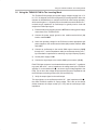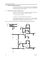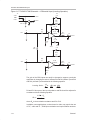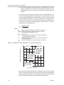
1
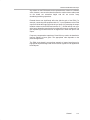
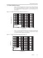
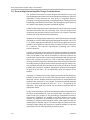
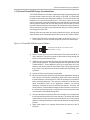
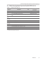
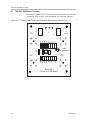
THS4012 Dual High Speed Operational Amplifier Evaluation Module User’s Guide May 1999 Mixed-Signal Products SLOU041 IMPORTANT NOTICE Texas Instruments (TI) reserves the right to make changes to its products or to discontinue any semiconductor product or service without notice, and advises its customers to obtain the latest version of relevant information to verify, before placing orders, that the information being relied on is current. TI warrants performance of its semiconductor products and related software to the specifications applicable at the time of sale in accordance with TI’s standard warranty. Testing and other quality control techniques are utilized to the extent TI deems necessary to support this warranty. Specific testing of all parameters of each device is not necessarily performed, except those mandated by government requirements. Certain applications using semiconductor products may involve potential risks of death, personal injury, or severe property or environmental damage (“Critical Applications”). TI SEMICONDUCTOR PRODUCTS ARE NOT DESIGNED, INTENDED, AUTHORIZED, OR WARRANTED TO BE SUITABLE FOR USE IN LIFE-SUPPORT APPLICATIONS, DEVICES OR SYSTEMS OR OTHER CRITICAL APPLICATIONS. Inclusion of TI products in such applications is understood to be fully at the risk of the customer. Use of TI products in such applications requires the written approval of an appropriate TI officer. Questions concerning potential risk applications should be directed to TI through a local SC sales office. In order to minimize risks associated with the customer’s applications, adequate design and operating safeguards should be provided by the customer to minimize inherent or procedural hazards. TI assumes no liability for applications assistance, customer product design, software performance, or infringement of patents or services described herein. Nor does TI warrant or represent that any license, either express or implied, is granted under any patent right, copyright, mask work right, or other intellectual property right of TI covering or relating to any combination, machine, or process in which such semiconductor products or services might be or are used. Copyright 1999, Texas Instruments Incorporated Preface Related Documentation From Texas Instruments J THS4012 DUAL LOW-NOISE HIGH-SPEED OPERATIONAL AMPLIFIER (literature number SLOS216) This is the data sheet for the THS4012 operational amplifier integrated circuit that is used in the THS4012 evaluation module. FCC Warning This equipment is intended for use in a laboratory test environment only. It generates, uses, and can radiate radio frequency energy and has not been tested for compliance with the limits of computing devices pursuant to subpart J of part 15 of FCC rules, which are designed to provide reasonable protection against radio frequency interference. Operation of this equipment in other environments may cause interference with radio communications, in which case the user at his own expense will be required to take whatever measures may be required to correct this interference. Trademarks TI is a trademark of Texas Instruments Incorporated. Chapter Title—Attribute Reference iii iv Running Title—Attribute Reference Contents 1 General . . . . . . . . . . . . . . . . . . . . . . . . . . . . . . . . . . . . . . . . . . . . . . . . . . . . . . . . . . . . . . . . . . . . . . . . . 1-1 1.1 Feature Highlights . . . . . . . . . . . . . . . . . . . . . . . . . . . . . . . . . . . . . . . . . . . . . . . . . . . . . . . . . . 1-2 1.2 Description . . . . . . . . . . . . . . . . . . . . . . . . . . . . . . . . . . . . . . . . . . . . . . . . . . . . . . . . . . . . . . . . 1-3 1.3 THS4012 EVM Noninverting Operation . . . . . . . . . . . . . . . . . . . . . . . . . . . . . . . . . . . . . . . . 1-4 1.4 Using The THS4012 EVM In The Noninverting Mode . . . . . . . . . . . . . . . . . . . . . . . . . . . . 1-6 1.5 THS4012 EVM Inverting Operation . . . . . . . . . . . . . . . . . . . . . . . . . . . . . . . . . . . . . . . . . . . 1-7 1.6 Using The THS4012 EVM In The Inverting Mode . . . . . . . . . . . . . . . . . . . . . . . . . . . . . . . 1-9 1.7 THS4012 EVM Differential Input . . . . . . . . . . . . . . . . . . . . . . . . . . . . . . . . . . . . . . . . . . . . . 1-10 1.8 Using The THS4012 EVM WIth Differential Inputs . . . . . . . . . . . . . . . . . . . . . . . . . . . . . . 1-14 1.9 THS4012 EVM Specifications . . . . . . . . . . . . . . . . . . . . . . . . . . . . . . . . . . . . . . . . . . . . . . . 1-14 1.10 THS4012 EVM Performance . . . . . . . . . . . . . . . . . . . . . . . . . . . . . . . . . . . . . . . . . . . . . . . . 1-15 1.11 General High-Speed Amplifier Design Considerations . . . . . . . . . . . . . . . . . . . . . . . . . . 1-16 1.12 General PowerPAD Design Considerations . . . . . . . . . . . . . . . . . . . . . . . . . . . . . . . . . . . 1-17 2 Reference . . . . . . . . . . . . . . . . . . . . . . . . . . . . . . . . . . . . . . . . . . . . . . . . . . . . . . . . . . . . . . . . . . . . . . . 2.1 THS4012 EVM Complete Schematic . . . . . . . . . . . . . . . . . . . . . . . . . . . . . . . . . . . . . . . . . . 2.1 THS4012 Dual High-Speed Operational Amplifier EVM Parts List . . . . . . . . . . . . . . . . . 2.2 THS4012 EVM Board Layouts . . . . . . . . . . . . . . . . . . . . . . . . . . . . . . . . . . . . . . . . . . . . . . . . Chapter Title—Attribute Reference 2-1 2-2 2-3 2-4 v Running Title—Attribute Reference Figures 1–1 1–2 1–3 1–4 1–5 1–6 1–7 1–8 1–9 THS4012 Evaluation Module . . . . . . . . . . . . . . . . . . . . . . . . . . . . . . . . . . . . . . . . . . . . . . . . . . . 1-3 THS4012 EVM Schematic — Noninverting Operation . . . . . . . . . . . . . . . . . . . . . . . . . . . . . . 1-4 THS4012 EVM Schematic — Inverting Operation . . . . . . . . . . . . . . . . . . . . . . . . . . . . . . . . . 1-7 THS4012 EVM Schematic — Differential Input (Noninverting Operation) . . . . . . . . . . . . 1-10 THS4012 EVM Schematic — Differential Input (Inverting Operation) . . . . . . . . . . . . . . . . 1-12 THS4012 EVM Frequency Response with Gain = 2 . . . . . . . . . . . . . . . . . . . . . . . . . . . . . . . 1-15 THS4012 EVM Phase Response with Gain = 2 . . . . . . . . . . . . . . . . . . . . . . . . . . . . . . . . . . 1-15 PowerPAD PCB Etch and Via Pattern . . . . . . . . . . . . . . . . . . . . . . . . . . . . . . . . . . . . . . . . . . . 1-17 Maximum Power Dissipation vs Free-Air Temperature . . . . . . . . . . . . . . . . . . . . . . . . . . . . 1-18 2–1 2–2 2–2 2–3 THS4012 EVM Schematic . . . . . . . . . . . . . . . . . . . . . . . . . . . . . . . . . . . . . . . . . . . . . . . . . . . . . . THS4012 EVM Component Placement Silkscreen and Solder Pads . . . . . . . . . . . . . . . . . THS4012 EVM PC Board Layout – Component Side . . . . . . . . . . . . . . . . . . . . . . . . . . . . . . . THS4012 EVM PC Board Layout – Back Side . . . . . . . . . . . . . . . . . . . . . . . . . . . . . . . . . . . . 2-2 2-4 2-5 2-6 Tables 2–1 vi THS4012 EVM Parts List . . . . . . . . . . . . . . . . . . . . . . . . . . . . . . . . . . . . . . . . . . . . . . . . . . . . . . . 2-3 Chapter 1 General This chapter details the Texas Instruments (TI) THS4012 dual high-speed operational amplifier evaluation module (EVM), SLOP230. It includes a list of EVM features, a brief description of the module illustrated with a pictorial and a schematic diagram, EVM specifications, details on connecting and using the EVM, and discussions on high-speed amplifier design and thermal considerations. Topic Page 1.1 Feature Highlights . . . . . . . . . . . . . . . . . . . . . . . . . . . . . . . . . . . . . . . . . . . . 1–2 1.2 Description . . . . . . . . . . . . . . . . . . . . . . . . . . . . . . . . . . . . . . . . . . . . . . . . . . . 1–3 1.3 THS4012 EVM Noninverting Operation . . . . . . . . . . . . . . . . . . . . . . . . . . 1–4 1.4 Using The THS4012 EVM In The Noninverting Mode . . . . . . . . . . . . . 1–6 1.5 THS4012 EVM Inverting Operation . . . . . . . . . . . . . . . . . . . . . . . . . . . . . . 1–7 1.6 Using The THS4012 EVM In The Inverting Mode . . . . . . . . . . . . . . . . . 1–9 1.7 THS4012 EVM Differential Input . . . . . . . . . . . . . . . . . . . . . . . . . . . . . . 1–10 1.8 Using The THS4012 EVM With Differential Inputs . . . . . . . . . . . . . . 1–14 1.9 THS4012 EVM Specifications . . . . . . . . . . . . . . . . . . . . . . . . . . . . . . . . . 1–14 1.10 THS4012 EVM Performance . . . . . . . . . . . . . . . . . . . . . . . . . . . . . . . . . . 1–15 1.11 General High-Speed Amplifier Design Considerations . . . . . . . . . 1–16 1.12 General PowerPAD Design Considerations . . . . . . . . . . . . . . . . . . . . 1–17 General 1-1 Feature Highlights 1.1 Feature Highlights THS4012 Dual High-Speed Operational Amplifier EVM features include: J J J J J J J 1-2 High Bandwidth — 75 MHz, –3 dB at ± 15 VCC and Gain = 2 ± 5-V to ± 15-V Operation Noninverting Single-Ended Inputs — Inverting-Capable Through Component Change Module Gain Set to 2 (Noninverting) — Adjustable Through Component Change Nominal 50-Ω Impedance Inputs and Outputs Standard SMA Input and Output Connectors Good Example of High-Speed Amplifier Design and Layout General Description 1.2 Description The TI THS4012 dual high-speed operational amplifier evaluation module (EVM) is a complete dual high-speed amplifier circuit. It consists of the TI THS4012 dual low-noise high-speed operational amplifier IC, along with a small number of passive parts, mounted on a small circuit board measuring approximately 1.9 inch by 2.2 inch (Figure 1–1). The EVM uses standard SMA miniature RF connectors for inputs and outputs and is completely assembled, tested, and ready to use — just connect it to power, a signal source, and a load (if desired). Figure 1–1. THS4012 Evaluation Module –VCC GND +VCC + C1 J2 J1 Vin1 + C2 J3 Vout1 R7 C3 R6 R5 R4 R3 R2 R1 U1 C5 C4 R8 TEXAS INSTRUMENTS J4 Vin2 J5 Vout2 R15 C6 R14 R13 R12 R11 R10 R9 SLOP230 THS4012 EVM Board Note: The EVM is shipped with the following component locations empty: C3, C6, R2, R4, R8, R10, R12 Although the THS4012 EVM is shipped with components installed for dual-channel single-ended noninverting operation, it can also be configured for single-channel differential and/or inverting operation by moving components. Noninverting gain is set to 2 with the installed components. The input of each channel is terminated with a 50-Ω impedance to provide correct line impedance matching. The amplifier IC outputs are routed through 50-Ω resistors both to provide correct line impedance matching and to help isolate capacitive loading on the outputs of the amplifier. Capacitive loading directly on the output of the IC decreases the amplifier’s phase margin and can result in peaking or oscillations. General 1-3 THS4012 EVM Noninverting Operation 1.3 THS4012 EVM Noninverting Operation The THS4012 EVM is shipped preconfigured for dual-channel noninverting operation, as shown in Figure 1–2. Note that compensation capacitors C3 and C6 are not installed. Figure 1–2. THS4012 EVM Schematic — Noninverting Operation C3 x µF J2 –VCC GND +VCC 1 –VCC 2 3 C2 6.8 µF C1 6.8 µF +VCC R5 1 kΩ R6 1 kΩ 2 +VCC C5 0.1 µF 8 U1:A THS4012 – J1 R7 49.9 Ω J3 Vout1 1 Vin1 R1 49.9 Ω R3 0Ω 3 + C4 0.1 µF 4 –VCC C6 x µF R13 1 kΩ R14 1 kΩ 6 – J4 Vin2 R9 49.9 Ω R11 0Ω 5 + U1:B THS4012 R15 49.9 Ω J5 Vout2 7 The gain of the EVM can easily be changed to support a particular application by simply changing the ratio of resistors R6 and R5 (channel 1) and R14 and R13 (channel 2) as described in the following equation: Noninverting Gain + 1 ) RRF + 1 ) RR65 G and 1 ) RR14 13 In addition, some applications, such as those for video, may require the use of 75-Ω cable and 75-Ω EVM input termination and output isolation resistors. 1-4 General THS4012 EVM Noninverting Operation Any of the resistors on the EVM board can be replaced with a resistor of a different value; however, care must be taken because the surface-mount solder pads on the board are somewhat fragile and will not survive many desoldering/soldering operations. External factors can significantly affect the effective gain of the EVM. For example, connecting test equipment with 50-Ω input impedance to the EVM output will divide the output signal level by a factor of 2 (assuming the output isolation resistor on the EVM board remains 50 Ω). Similar effects can occur at the input, depending upon how the input signal sources are configured. The gain equations given above assume no signal loss in either the input or the output. Frequency compensation capacitors C3 and C6 may need to be installed to improve stability at lower gains. The appropriate value depends on the particular application. The EVM circuit board is an excellent example of proper board layout for high-speed amplifier designs and can be used as a guide for user application board layouts. General 1-5 Using the THS4012 EVM In The Noninverting Mode 1.4 Using the THS4012 EVM In The Noninverting Mode The THS4012 EVM operates from power-supply voltages ranging from ± 5 V to ± 15 V. As shipped, the EVM is configured for inverting operation and the gain is set to 4. Signal inputs on the module are terminated for 50-Ω nominal source impedance. An oscilloscope is typically used to view and analyze the EVM output signal. 1) Ensure that all power supplies are set to OFF before making power supply connections to the THS4012 EVM. 2) Connect the power supply ground to the module terminal block (J2) location marked GND. 3) Select the operating voltage for the EVM and connect appropriate split power supplies to the module terminal block (J2) locations marked –VCC and +VCC. 4) Connect an oscilloscope to the module SMA output connector (J3/J5) through a 50-Ω nominal impedance cable (an oscilloscope having a 50-Ω input termination is preferred for examining very high frequency signals). 5) Set the power supply to ON. 6) Connect the signal input to the module SMA input connector (J1/J4). Each EVM input connector is terminated with a 50-Ω impedance to ground. With a 50-Ω source impedance, the voltage seen by the THS4012 amplifier IC on the module will be the source signal voltage applied to the EVM. This is due to the voltage division between the source impedance and the EVM input terminating resistors (R1, R9). ½ 7) Verify the output signal on the oscilloscope. ½ The signal shown on an oscilloscope with a 50-Ω input impedance will be the actual THS4012 amplifier IC output voltage. This is due to the voltage division between the output resistor (R7, R15) and the oscilloscope input impedance. 1-6 General THS4012 EVM Inverting Operation 1.5 THS4012 EVM Inverting Operation Although the THS4012 EVM is shipped preconfigured for dual-channel noninverting operation, it can be reconfigured for inverting operation by making the following component changes: 1) Move resistor R3 to the R2 location and R5 to the R4 location on the board. 2) Move resistor R11 to the R10 location and R13 to the R12 location on the board. This configuration is shown in Figure 1–3. Note that compensation capacitors C3 and C6 are not installed. Figure 1–3. THS4012 EVM Schematic — Inverting Operation C3 x µF J2 –VCC GND +VCC 1 –VCC 2 3 C2 6.8 µF C1 6.8 µF +VCC R6 1 kΩ +VCC R4 1 kΩ J1 Vin1 2 R1 49.9 Ω – C5 0.1 µF U1:A THS4012 8 R7 49.9 Ω J3 Vout1 1 3 + C4 0.1 µF 4 R2 0Ω C6 x µF –VCC R14 1 kΩ R12 1 kΩ J4 Vin2 6 R9 49.9 Ω – U1:B THS4012 R15 49.9 Ω Vout2 7 5 J5 + R10 0Ω General 1-7 THS4012 EVM Inverting Operation The gain of the EVM can easily be changed to support a particular application by changing the ratio of resistors R6 and R4 (channel 1) and R14 and R12 (channel 2) as described in the following equation: Inverting Gain F + –R + –RR46 R G and –R14 R12 In addition, some applications, such as those for video, may require the use of 75-Ω cable and 75-Ω EVM input termination and output isolation resistors. Because the noninverting terminals are at ground potential, the inverting terminal becomes a virtual ground and is held to 0 V. This causes the input impedance to ground at the input terminal to look like two resistors in parallel (R1 and R4 for channel 1, and R9 and R12 for channel 2). As a result, if the source termination is changed, R1 and R9 must be adjusted in accordance with the following equations: R1 + RR44–RR T (Channel 1) T and R9 R + R12 R4–R T (Channel 2) T where RT is the source impedance. Any resistor on the EVM board can be replaced with a resistor of a different value; however, care must be taken because the surface-mount solder pads on the board are somewhat fragile and will not survive many desoldering/soldering operations. External factors can significantly affect the effective gain of the EVM. For example, connecting test equipment with 50-Ω input impedance to the EVM output will divide the output signal level by a factor of 2 (assuming the output isolation resistor on the EVM board remains 50 Ω). Similar effects can occur at the input, depending upon how the input signal sources are configured. The gain equations given above assume no signal loss in either the input or the output. Frequency compensation capacitors C3 and C6 may need to be installed to improve stability at lower gains. The appropriate value depends on the particular application. The EVM circuit board is an excellent example of proper board layout for high-speed amplifier designs and can be used as a guide for user application board layouts. 1-8 General Using the THS4012 EVM In The Inverting Mode 1.6 Using the THS4012 EVM In The Inverting Mode The THS4012 EVM operates from power-supply voltages ranging from ± 5 V to ± 15 V. As shipped, the EVM is configured for inverting operation. Move the resistors as detailed above to configure the EVM for noninverting operation, which sets the gain to –3. Signal inputs on the module are terminated for 50-Ω nominal source impedance. An oscilloscope is typically used to view and analyze the EVM output signal. 1) Ensure that all power supplies are set to OFF before making power supply connections to the THS4012 EVM. 2) Connect the power supply ground to the module terminal block (J2) location marked GND. 3) Select the operating voltage for the EVM and connect appropriate split power supplies to the module terminal block (J2) locations marked –VCC and +VCC. 4) Connect an oscilloscope to the module SMA output connector (J3/J5) through a 50-Ω nominal impedance cable (an oscilloscope having a 50-Ω input termination is preferred for examining very high frequency signals). 5) Set the power supply to ON. 6) Connect the signal input to the module SMA input connector (J1/J2). Each EVM input connector is terminated with an equivalent 50-Ω impedance to ground. With a 50-Ω source impedance, the voltage seen by the THS4012 amplifier IC on the module will be the source signal voltage applied to the EVM. This is due to the voltage division between the source impedance and the EVM input terminating resistors (R1 || R4 and R9 || R12). ½ 7) Verify the output signal on the oscilloscope. ½ The signal shown on an oscilloscope with a 50-Ω input impedance will be the actual THS4012 amplifier IC output voltage. This is due to the voltage division between the output resistor (R7, R15) and the oscilloscope input impedance. General 1-9 THS4012 EVM Differential Input 1.7 THS4012 EVM Differential Input The THS4012 EVM is shipped preconfigured for dual-channel, single-ended noninverting operation. It can be reconfigured for single-channel, differential operation, either noninverting or inverting. 1.7.1 Differential Input, Noninverting Operation Configure the THS4012 EVM for differential noninverting operation by removing two resistors and adding a resistor on the board: 1) Remove resistors R1 and R9. 2) Add a 100-Ω resistor to the R8 location on the board. This configuration (noninverting) is shown in Figure 1–4. For a noninverting differential input, R8 should be 100 Ω to match 50-Ω source impedances. Note that compensation capacitors C3 and C6 are not installed. Figure 1–4. THS4012 EVM Schematic — Differential Input (Noninverting Operation) C3 x µF J2 –VCC GND +VCC 1 –VCC 2 3 C2 6.8 µF C1 6.8 µF +VCC R5 1 kΩ R6 1 kΩ +VCC 2 R3 0Ω J1 Vin1 – 8 C5 0.1 µF U1:A THS4012 + C6 x µF –VCC R13 1 kΩ R14 1 kΩ 6 1-10 Vout1 C4 0.1 µF 4 R8 100 Ω Vin2 J3 1 3 J4 R7 49.9 Ω R11 0Ω 5 – + U1:B THS4012 7 R15 49.9 Ω J5 Vout2 General THS4012 EVM Differential Input The gain of the EVM can easily be changed to support a particular application by simply changing the ratio of resistors R6 and R5 (channel 1) and R14 and R13 (channel 2) as described in the following equation: Noninverting Gain + 1 ) RRF + 1 ) RR65 G and 1 ) RR14 13 In addition, some applications, such as those for video, may require the use of 75-Ω cable and 75-Ω EVM input termination and output isolation resistors. Any of the resistors on the EVM board can be replaced with a resistor of a different value; however, care must be taken because the surface-mount solder pads on the board are somewhat fragile and will not survive many desoldering/soldering operations. External factors can significantly affect the effective gain of the EVM. For example, connecting test equipment with 50-Ω input impedance to the EVM output will divide the output signal level by a factor of 2 (assuming the output isolation resistor on the EVM board remains 50 Ω). Similar effects can occur at the input, depending upon how the input signal sources are configured. The gain equations given above assume no signal loss in either the input or the output. Frequency compensation capacitors C3 and C6 may need to be installed to improve stability at lower gains. The appropriate value depends on the particular application. The EVM circuit board is an excellent example of proper board layout for high-speed amplifier designs and can be used as a guide for user application board layouts. 1.7.2 Differential Input, Inverting Operation Configure the THS4012 EVM for differential inverting operation by removing two resistors and adding a resistor on the board: 1) Move resistor R3 to the R2 location and R5 to the R4 location on the board. 2) Move resistor R11 to the R10 location and R13 to the R12 location on the board. 3) Remove resistors R1 and R9. 4) Add a 100-Ω resistor to the R8 location on the board. This configuration (inverting) is shown in Figure 1–5. For a inverting differential input, R8 should be 200 Ω to match a 50-Ω source impedance. Note that compensation capacitors C3 and C6 are not installed. General 1-11 THS4012 EVM Differential Input Figure 1–5. THS4012 EVM Schematic — Differential Input (Inverting Operation) C3 x µF J2 –VCC GND +VCC 1 –VCC 2 3 C2 6.8 µF C1 6.8 µF +VCC R6 1 kΩ +VCC R4 1 kΩ J1 2 Vin1 – 8 C5 0.1 µF U1:A THS4012 R7 49.9 Ω J3 Vout1 1 3 + C4 0.1 µF 4 R2 0Ω C6 x µF –VCC R8 100 Ω R14 1 kΩ R12 1 kΩ J4 6 Vin2 5 – U1:B THS4012 + R15 49.9 Ω 7 J5 Vout2 R10 0Ω The gain of the EVM inputs can easily be changed to support a particular application by changing the ratio of resistors R6 and R4 (channel 1) and R14 and R12 (channel 2) as described in the following equation: Inverting Gain 6 F + –R + –R R R4 G and –R14 R12 R4 and R12 form part of the input impedance and R8 should be adjusted in accordance with the following equation: R8 + 2 RR44–RTRT where RT is the termination resistance and R4 = R12. In addition, some applications, such as those for video, may require the use of 75-Ω cable and 75-Ω EVM input termination and output isolation resistors. 1-12 General THS4012 EVM Differential Input Any resistor on the EVM board can be replaced with a resistor of a different value; however, care must be taken because the surface-mount solder pads on the board are somewhat fragile and will not survive many desoldering/soldering operations. External factors can significantly affect the effective gain of the EVM. For example, connecting test equipment with 50-Ω input impedance to the EVM output will divide the output signal level by a factor of 2 (assuming the output isolation resistor on the EVM board remains 50 Ω). Similar effects can occur at the input, depending upon how the input signal sources are configured. The gain equations given above assume no signal loss in either the input or the output. Frequency compensation capacitors C3 and C6 may need to be installed to improve stability at lower gains. The appropriate value depends on the particular application. The EVM circuit board is an excellent example of proper board layout for high-speed amplifier designs and can be used as a guide for user application board layouts. General 1-13 Using the THS4012 EVM With Differential Inputs 1.8 Using the THS4012 EVM With Differential Inputs The THS4012 EVM operates from power-supply voltages ranging from ± 5 V to ± 15 V. Move resistors on the board as detailed above for either noninverting or inverting operation to configure the EVM for differential input operation. Signal inputs on the module are terminated for 50-Ω nominal source impedance. An oscilloscope is typically used to view and analyze the EVM output signal. 1) Ensure that all power supplies are set to OFF before making power supply connections to the THS4012 EVM. 2) Connect the power supply ground to the module terminal block (J2) location marked GND. 3) Select the operating voltage for the EVM and connect appropriate split power supplies to the module terminal block (J2) locations marked –VCC and +VCC. 4) Connect an oscilloscope across the module SMA output connectors (J3 and J5) through a 50-Ω nominal impedance cable (an oscilloscope having a 50-Ω input termination is preferred for examining very high frequency signals). 5) Set the power supply to ON. 6) Connect the differential signal input across the module SMA input connectors (J1 and J4) The differential EVM input is terminated with an equivalent 50-Ω impedance for each input. With a 50-Ω source impedance, the voltage seen by the THS4012 amplifier IC on the module will be the source signal voltage applied to the EVM. This is due to the voltage division between the source impedance and the EVM equivalent input resistance. ½ 7) Verify the differential output signal on the oscilloscope. ¼ The signal shown on an oscilloscope with a 50-Ω input impedance will be the actual THS4012 amplifier IC output voltage. This is due to the voltage division between the output resistors (R7, R15) and the oscilloscope input impedance. 1.9 THS4012 EVM Specifications Supply voltage range, ± VCC . . . . . . . . . . . . . . . . . . . . . . . . . . . . ± 5 V to ± 15 V Supply current, ICC . . . . . . . . . . . . . . . . . . . . . . . . . . . . . . . . . . . . . . . 17 mA typ Input voltage, VI . . . . . . . . . . . . . . . . . . . . . . . . . . . . . . . . . . . . . . . . . ± VCC, max Output drive, IO . . . . . . . . . . . . . . . . . . . . . . . . . . . . . . . . . . . . . . . . . . . . . 90 mA For complete THS4012 amplifier IC specifications and parameter measurement information, and additional application information, see the THS4012 data sheet, TI Literature Number SLOS216. 1-14 General THS4012 EVM Performance 1.10 THS4012 EVM Performance Figure 1–6 shows the typical frequency response of the THS4012 EVM using the noninverting configuration (G = 2). Typical – 0.1 dB bandwidth is 25 MHz and – 3-dB bandwidth is 75 MHz with both a ±15-V power supply and a ±5-V power supply. Figure 1–6. THS4012 EVM Frequency Response with Gain = 2 7 6 Output Amplitude – dB 5 4 3 2 1 VCC = ±5 V and ± 15 V VO = 0.2 VRMS RL = 150 Ω 0 –1 100k 1M 10M 100M 500M f – Frequency – Hz Figure 1–7 shows the typical phase response of the THS4012 EVM using the noninverting configuration (G = 2). This shows a 75° phase margin for both ±15-V and ±5-V power supplies on both channels. Figure 1–7. THS4012 EVM Phase Response with Gain = 2 45 Output Phase – ° 0 –45 –90 –135 –180 –225 100k VCC = ±5 V and ± 15 V VO = 0.2 VRMS RL = 150 Ω 1M 10M 100M 500M f – Frequency – Hz General 1-15 General High-Speed Amplifier Design Considerations 1.11 General High-Speed Amplifier Design Considerations The THS4012 EVM layout has been designed and optimized for use with high-speed signals and can be used as an example when designing THS4012 applications. Careful attention has been given to component selection, grounding, power supply bypassing, and signal path layout. Disregard of these basic design considerations could result in less than optimum performance of the THS4012 high-speed, low-power operational amplifier. Surface-mount components were selected because of the extremely low lead inductance associated with this technology. Also, because surface-mount components are physically small, the layout can be very compact. This helps minimize both stray inductance and capacitance. Tantalum power supply bypass capacitors (C1 and C2) at the power input pads help supply currents for rapid, large signal changes at the amplifier output. The 0.1 µF power supply bypass capacitors (C4 and C5) were placed as close as possible to the IC power input pins in order to keep the PCB trace inductance to a minimum. This improves high-frequency bypassing and reduces harmonic distortion. A proper ground plane on both sides of the PCB should always be used with high-speed circuit design. This provides low-inductive ground connections for return current paths. In the area of the amplifier IC input pins, however, the ground plane was removed to minimize stray capacitance and reduce ground plane noise coupling into these pins. This is especially important for the inverting pin while the amplifier is operating in the noninverting mode. Because the voltage at this pin swings directly with the noninverting input voltage, any stray capacitance would allow currents to flow into the ground plane, causing possible gain error and/or oscillation. Capacitance variations at the amplifier IC input pin of less than 1 pF can significantly affect the response of the amplifier. In general, it is always best to keep signal lines as short and as straight as possible. Round corners or a series of 45_ bends should be used instead of sharp 90_ corners. Stripline techniques should also be incorporated when signal lines are greater than 1 inch in length. These traces should be designed with a characteristic impedance of either 50 Ω or 75 Ω, as required by the application. Such signal lines should also be properly terminated with an appropriate resistor. Finally, proper termination of all inputs and outputs should be incorporated into the layout. Unterminated lines, such as coaxial cable, can appear to be a reactive load to the amplifier IC. By terminating a transmission line with its characteristic impedance, the amplifier’s load then appears to be purely resistive and reflections are absorbed at each end of the line. Another advantage of using an output termination resistor is that capacitive loads are isolated from the amplifier output. This isolation helps minimize the reduction in amplifier phase-margin and improves the amplifier stability for improved performance such as reduced peaking and settling times. 1-16 General General PowerPAD Design Considerations 1.12 General PowerPAD Design Considerations The THS4012DGN IC is mounted in a special package incorporating a thermal pad that transfers heat from the IC die directly to the PCB. The PowerPAD package is constructed using a downset leadframe. The die is mounted on the leadframe but is electrically isolated from it. The bottom surface of the lead frame is exposed as a metal thermal pad on the underside of the package and makes physical contact with the PCB. Because this thermal pad is in direct physical contact with both the die and the PCB, excellent thermal performance can be achieved by providing a good thermal path away from the thermal pad mounting point on the PCB. Although there are many ways to properly heatsink this device, the following steps illustrate the recommended approach as used on the THS4012 EVM. 1) Prepare the PCB with a top side etch pattern as shown in Figure 1–8. There should be etch for the leads as well as etch for the thermal pad. Figure 1–8. PowerPAD PCB Etch and Via Pattern Thermal pad area (68 mils x 70 mils) with 5 vias (Via diameter = 13 mils) 2) Place five holes in the area of the thermal pad. These holes should be 13 mils in diameter. They are kept small so that solder wicking through the holes is not a problem during reflow. 3) Additional vias may be placed anywhere along the thermal plane outside of the thermal pad area. This helps dissipate the heat generated by the THS4012DGN IC. These additional vias may be larger than the 13-mil diameter vias directly under the thermal pad They can be larger because they are not in the thermal pad area to be soldered so that wicking is not a problem. 4) Connect all holes to the internal ground plane. 5) When connecting these holes to the ground plane, do not use the typical web or spoke via connection methodology. Web connections have a high thermal resistance connection that is useful for slowing the heat transfer during soldering operations. This makes the soldering of vias that have plane connections easier. In this application, however, low thermal resistance is desired for the most efficient heat transfer. Therefore, the holes under the THS4012DGN package should make their connection to the internal ground plane with a complete connection around the entire circumference of the plated-through hole. 6) The top-side solder mask should leave the terminals of the package and the thermal pad area with its five holes exposed. The bottom-side solder mask should cover the five holes of the thermal pad area. This prevents solder from being pulled away from the thermal pad area during the reflow process. 7) Apply solder paste to the exposed thermal pad area and all of the IC terminals. General 1-17 General PowerPAD Design Considerations 8) With these preparatory steps in place, the THS4012DGN IC is simply placed in position and run through the solder reflow operation as any standard surface-mount component. This results in a part that is properly installed. The actual thermal performance achieved with the THS4012DGN in its PowerPAD package depends on the application. In the example above, if the size of the internal ground plane is approximately 3 inches × 3 inches, then the expected thermal coefficient, θJA, is about 58.4_C/W. For comparison, the non-PowerPAD version of the THS4012 IC (D-package in SOIC) is shown. For a given θJA, the maximum power dissipation is shown in Figure 1–9 and is calculated by the following formula: P D + Where: ǒ Ǔ T –T MAX A q JA PD = Maximum power dissipation of THS4012 IC (watts) TMAX = Absolute maximum junction temperature (150°C) TA = Free-ambient air temperature (°C) θJA = θJC + θCA θJC = Thermal coefficient from junction to case (4.7°C/W) for THS4012DGN (PowerPAD) θJC = Thermal coefficient from junction to case (38.3°C/W) for THS4012D (SOIC) θCA = Thermal coefficient from case to ambient air (°C/W) Figure 1–9. Maximum Power Dissipation vs Free-Air Temperature Maximum Power Dissipation – W 3.5 TJ = 150°C No Air Flow 3 DGN Package θJA = 58.4°C/W 2 oz Trace and Copper Pad with Solder 2.5 2 DGN Package θJA = 158°C/W 2 oz Trace and Copper Pad without Solder 1.5 1 .5 0 –40 THS4012 SOIC – Package θJA = 166.7°C/W –20 0 20 40 60 80 100 TA – Free-Air Temperature – °C Even though the THS4012 EVM PCB is smaller than the one in the example above, the results should give an idea of how much power can be dissipated by the PowerPAD IC package. The THS4012 EVM is a good example of proper thermal management when using PowerPAD-mounted devices. 1-18 General General PowerPAD Design Considerations Correct PCB layout and manufacturing techniques are critical for achieving adequate transfer of heat away from the PowerPAD IC package. More details on proper board layout can be found in the THS4012 Low-noise Dual Differential Receiver data sheet (SLOS216). For more general information on the PowerPAD package and its thermal characteristics, see the Texas Instruments Technical Brief, PowerPAD Thermally Enhanced Package (SLMA002). General 1-19 1-20 General Chapter 2 Reference This chapter includes a complete schematic, parts list, and PCB layout illustrations for the THS4012 EVM. Topic Page 2.1 THS4012 EVM Complete Schematic . . . . . . . . . . . . . . . . . . . . . . . . . . . . 2–2 2.1 THS4012 Dual High-Speed Operational Amplifier EVM Parts List . . 2–3 2.2 THS4012 EVM Board Layouts . . . . . . . . . . . . . . . . . . . . . . . . . . . . . . . . . . 2–4 Reference 2-1 THS4012 EVM Complete Schematic 2.1 THS4012 EVM Complete Schematic Figure 2–1 shows the complete THS4012 EVM schematic. The EVM is shipped preconfigured for dual-channel, single-ended inverting operation. Components showing a value of X are not supplied on the board, but can be installed by the user to reconfigure the EVM for noninverting and/or differential operation. Figure 2–1. THS4012 EVM Schematic C3 x µF J2 –VCC GND +VCC 1 –VCC 2 3 C1 6.8 µF C2 6.8 µF +VCC R5 1 kΩ R6 1 kΩ +VCC R4 xΩ J1 2 – 8 U1:A THS4012 VIN1 R1 49.9 Ω C5 0.1 µF R7 49.9 Ω J3 VOUT1 1 R3 0Ω 3 + C4 0.1 µF 4 R2 xΩ –VCC R8 xΩ C6 x µF R13 1 kΩ R12 xΩ J4 R14 1 kΩ 6 – VIN2 R9 49.9 Ω U1:B THS4012 7 R11 0Ω 5 R15 49.9 Ω J5 VOUT2 + R10 xΩ 2-2 Reference THS4012 Dual High-Speed Operational Amplifier EVM Parts List 2.2 THS4012 Dual High-Speed Operational Amplifier EVM Parts List Table 2–1. THS4012 EVM Parts List Reference Description Size Manufacturer/Supplier Part Number C1, C2 Capacitor, 6.8 µF, 35 V, Tantalum, SM C4, C5 Capacitor, 0.1 µF, Ceramic, 10%, SM J2 3-Pin Terminal Block (On Shore Tech.) Digi-Key ED1515–ND J1, J3, J4, J5 Connector, SMA 50-Ω vertical PC mount, throughhole Amphenol ARF1205–ND R1, R7, R9, R15 Resistor, 49.9 Ω, 1%, 1/8 W, SM 1206 R5, R6, R13, R14 Resistor, 1 kΩ, 1%, 1/8 W, SM 1206 R3, R11 Resistor, 0 Ω, 1/8 W, SM U1 IC, THS4012 amplifier R2, R4, R10, R12 Resistor, X Ω, 1%, 1/8 W, SM † C3, C6 Capacitor, X µF, 10%, Ceramic, SM † Sprague 293D685X9035D2T 1206 MuRata GRM42X7R104K50 1206 SOIC-8 TI THS4012DGN 1206 4–40 Hex Standoffs, 0.625′′ length, 0.25′′ O.D. 4–40 Screws PCB1 PCB, THS4012 EVM SLOP230 † These components are NOT supplied on the EVM and are to be determined and installed by the user to reconfigure the EVM in accordance with application requirements. Reference 2-3 THS4012 EVM Board Layouts 2.3 THS4012 EVM Board Layouts Board layout examples of the THS4012 EVM PCB are shown in the following illustrations. They are not to scale and appear here only as a reference. Figure 2–2. THS4012 EVM Component Placement Silkscreen and Solder Pads –VCC GND +VCC + J1 Vin1 C1 J3 Vout1 J2 + C2 R7 C3 R6 R5 R4 R3 R2 R1 U1 C5 C4 R8 TEXAS INSTRUMENTS J5 Vout2 J4 Vin2 R15 C6 R14 R13 R12 R11 R10 R9 SLOP230 THS4012 EVM Board 2-4 Reference THS4012 EVM Board Layouts Figure 2–3. THS4012 EVM PC Board Layout – Component Side Reference 2-5 THS4012 EVM Board Layouts Figure 2–4. THS4012 EVM PC Board Layout – Back Side 2-6 Reference