1
.,
{Z~m
~~~ffiJ~~
m(IDilloo[ID
~(ID~~~TIT 00
ZCB SINGLE OOARD <n1Pl1l'ER
Revision 1
USER t S MANUAL
Revision B
June 11, 1980
Copyright 1980
'Vector Graphic Inc.
7200-0203-03-02
COpyright 1980 by Vector Graphic Inc.
All rights resetved.
Disclaimer
Vector Graphic makes no representations or warranties with respect to the
contents of this manual itself, whether or not the product it describes is
covered by a warranty or repair agreeJIW::!nt. Further, Vector Graphic resetves
the right to revise this publication and to make changes from time to time
in the content hereof without obligation of Vector Graphic to notify any
person of such revision or changes, except when an agreement to the contrary
exists.
Revisions
The date and rev~s~on of each page herein appears at the bottom of each
page. The revision letter such as A or B changes if the MANUAL has been
improved but the PRODUCT itself has not been significantly Irodified. The
date and revision on the Title Page corresponds to that of the page most
recently revised. When the product itself is Irodified significantly, the
product will get a new revision nunber, as shown on the manual's title page,
and the manual will revert to revision A, as if it were treating a brand new
product. EAQi MANUAL SHOOID rnLY BE USED WITH mE PRODUCr IDENI'IFIED 00 mE
TrrLE PAGE.
Rev. I-B
6/11/80
Vector ZCB Single Board Computer
REPAIR AGREEMENl'
The ZCB Single Board Computer sold hereunder is sold lias is", with all
faults an:] without any warranty, either expressed or implied, including any
implied warranty of fitness for intended use or rerchantability. However,
the above notwithstanding, VECTOR GRAPHIC, INC., will, for a period of
ninety (90) days following delivery to custarer, repair or replace any ZCB
Single Board Computer that is found to contain defects in materials or
'Narkmanship, provided:
1. Such defect in naterial or 'Narkmanship exis ted at the time the
ZCB Single Board Computer left the VECI'OR GRAPHIC, INC., factory;
2. VECTOR GRAPHIC, INC., is given notice of t~e precise defect
claimed within ten (10) days after its discovery;
3. The ZCB Single Board Computer is promptly returned to VECTOR
GRAPHIC, INC., at customer's expense, for examination by VECI'OR GRMHIC,
INC., to confirm the alleged defect, and for subsequent repair or
replacement if found to be in order.
Repair, replacement or correction of any defects in naterial or 'Narkmanship
which are discovered after expiration of the period set forth above will be
perfo:r:med by VECTOR GRAPHIC, INC., at Buyer's expense, provided the ZCB
Single Board Computer is returned, also at Buyer's expense, to VECTOR
GRAPHIC, INC., for such repair, replacement or correction. In performing
any repair, replacement or correction after expiration of the period set
forth above, Buyer will be charged in addition to the cost of parts the
then-current VECTOR GRAPHIC, INC., repair rate. At the present time the
applicable rate is $35.00 for the first hour, am $18.00 per hour for every
hour of work required thereafter. Prior to commencing any repair,
replacement or correction of defects in naterial or 'Narkmanship discovered
after expiration of the period for no-cost-to-Buyer repairs, VECI'OR GRAPHIC,
INC., will sub:ni.t to Buyer a written estimate of the expected charges, and
VECTOR GRAPHIC, INC., will not commence repair until such time as the
written estimate of charges has been returned by Buyer to VECTOR GRAPHIC,
INC., signed by duly authorized representative authorizing VECTOR. GRMHIC,
INC., to ccrrm:mce with the repair work involved. VECTOR GRAPHIC, INC.,
shall have no obligation to repair, replace or correct any ZCB Single Board
Computer until the written estimate has been returned with approval to
proceed, and VECTOR. GRAIliIC, INC., nay at its option also require prepayrrent
of the estimated repair charges prior to commencing 'Nark.
Repair Agreement void if the enclosed card is not returned to VECTOR
GRAPHIC, INC. within ten (10) days of end consl..lIler purchase.
Rev. I-B 6/11/80
vector ZCB Single Board COmputer
FORlKJRD
Audience
This manual is intended for canputer
distributors, or others with at least a
moderate technical knowledge of small
I
<:XIlplters.
It will describe what the Vector Graphic
ZCB Single. Board Computer does in the context
of a canputer system, how to use the board
both in Vector Graphic and in other 8-100
systems, arrl how the board circuitry works.
Organization
Rev. 1-8 6/11/80
Each section is written at a uniform level
of technical depth. "Perspective" describes
WHAT the board does and requires only a
Jroderate know'ledge of canputer design •
. "User's Guide" describes HCW to make it do
things and assumes the same level of
knowledge, plus the abili ty to solder
jumpers and flip switches. "Theory of
Operation" discusses WHY the board works
and assumes a knowledge of d igi tal
electronics.
Vector ZCB Single Board canputer
TABLE OF CCNr:mrS
Section
Table of COntents
Specifications
I.
Perspective
1.1
1.2
1.3
1.4
1.5
The ZCB as a system •••••••••••••••••••••••••••••••••••••••• l-l
The ZCB as part of a system•••••••••••••••••••••••••••••••• l-l
CPU section •••••••••••••••••••••••••••••••••••••••••••••••• 1-1
EPROM/RAM section •••••••••••••••••••••••••••••••••••••••••• 1-2
I/O section •••••••••••••••••••••••••••••••••••••••••••••••• l-2
1.5.• 1
1.5.2
1.5.3
1.5.4
1.5.5
1.5.6
II.
Serial R:>rts Generally ••••••••••••••••••••••••••••••• 1-2
Serial Asynchronous Communications ••••••••••••••••••• 1-3
Serial Synchronous Communications •••••••••••••••••••• 1-3
RS-232C Theory ••••••••••••••••••••••••••••••••••••••• 1-4
RS-232C on the ZCB ••••••••••••••••••••••••••••••••••• l-S
Parallel Ports ••••••••••••••.•••••••••••••••••••••••• 1-6
User's Guide
2.1
Introduction ••••••••••••••••••••••••••••••••••••••••••••••• 2-1
2.1.1 Standard Jumpering and What it does ••••••••••••••••• 2-1
2.2
CPU Section •••••••••••••••••••••••••••••••••••••••••••••••• 2-1
2.2.1 Running the system at 2 or 4 MHz •••••••••••••••••••• 2-1
2.2.2 MWRITE enable/disable ••••••••••••••••••••••••••••••• 2-2
2.2.3 Auto WAIT state enable/disable •••••••••••••••••••••• 2-2
2.3
E!I?.RC:f\1~
SectiOl1 •••••••••••••••••••••••••••••••••••••••••• 2-2
2.3.1 2708 EPROM Addressing ••••••••••••••••••••••••••••••• 2-3
2.3.2 Auxi1iar-Y Memory Disab1e •••••••••••••••••••••••••••• 2-4
2.3.3 2716 EPROM Addressing ••••••••••••••••••••••••••••••• 2-5
2.3.4 2732 E!l?ROM Addressing ••••••••••••••••••••••••••••••• 2-6
2.3.5 Enable on-board EPROM on boot ••••••••••••••••••••••• 2-6
2.3.6 Phantom enable/disable •••••••••••••••••••••••••••••• 2-7
2.3.7 Jumper areas K, Land M••••••••••••••••••••••••••••• 2-7
2.4
I/O Sect i()l'1 •••••••••••••••••••••••••••••••••••••••••••••••• 2-7
2.4.1 I/O ]?()rt Address ing ••••••••• _•••••••••••••••••••••••• 2-7
2.4.2 Address Mirroring disable/enable •••••••••••••••••••• 2-9
2.4.3 Asynchronous Serial Baud Rate Selection ••••••••••••• 2-11
2.4.4 How' to connect rrost serial terminals ancl printers ••• 2-11
Rev. 1-6 6/11/80
Vector ZCB Single Board canputer
~
Section
2.4.5
2.4.6
2.4.7
2.4.S
2.4.9
2.9
How to connect most low speed acoustic couplers ••••• 2-15
Connecting additional RS-232C handshaking lines ••••• 2-15
USing the Parallel Ports •••••••••••••••••••••••••••• 2-1S
Connecting Sprint 3 to ZCB •••••••••••••••••••••••••• 2-19
Connecting vector MP to ZCB ••••••••••••••••••••••••• 2-19
Spare Chip and Patch areas ••••••••••••••••••••••••••••••••• 2-20
III. Theory of Operation
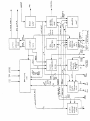
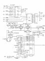
3.1 System Operation Block Diagram ••••••••••••••••••••••••••••• 3-1
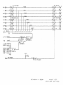
3.2 Serial Ports ••••••••••••••••••••••••••••••••••••••••••••••• 3-2
IV.
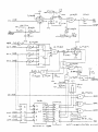
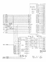
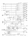
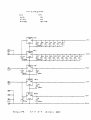
Schematics
Rev. 1-8 6/11/S0
Vector ZCB Single Board COmputer
SPECIFICATIONS-System
COmpatibility:
Most S-100 systans.
Power Requirements
+8VOC @ 970 rna. (typ.)
+16 VDC @ 120 rna.
-16 VDC @ 80 mao
Availability:
Shipped assembled, tested, burned in; no kits.
SPECIFICATIONS-EPRCM/RAM
Menory
65536 bytes addressable, 1024 bytes RAM on board,
3 EPRCM sockets on board, up to 12K addressable
EPRG1s included with
none
bJard
Menory Speed
RAM: 300ns.
EPRCI'1: User selected (450 ns. typical)
Menory Types
RAM: 2114 static
EPROM: 2708, 2716, 2732
Standard Location of
Systans r-bni tor EPRCM
EOOOH-E7FFH
Po\tler-0njReset Jump
Options
Auto boot on p.::lWer on/reset, jumps to merrory location
EOOOH. Shipped enabled.
SPECIFICATION5-CPU
Processor
Z-80A
Number of Da.ta Bits
8
Number of Address Bits
16
Instructions
158, including all 78 8080 instructions
Clock speed
2 or 4 MHz, jumper selectable, enabled for 4 MHz.
Interrupts
Z-80 r-bde 0 (8080 m:::de), MODE 1, MODE 2
I/O devices
256 I/O addresses
Dynamic RAM
Supports dynamic merrory by sending Z-80 RFSH
on bus line 66; fast reset/~r on clear signal
generated on board.
Rev. I-B
6/11/80
Vector ZCB Single Board Carplter
Static RAM
Fully compatible
MWRlTE
Jumper option to generate MWRITE on board
StaOOard: option enabled.
Wait state generation
for memories slower
than 300 ns.
3 options: generate one wait state on each bus
cycle, generate one wait state after each Ml
instruction, generate no wait states.
StaOOard: generate one wait state after each Ml
instruction.
.
Bus load
1 staOOard Tl'L load on all inputs
Buffering
Fan oot: 15 standard (60 low
Phantcm:
output buffer disable canpatible with Vector Graphic
EPRCM/RAM Boards, which generate phantan in resJ;OrlSe to
Fower-on-clear (POC). J1..IIIper selectable: on/off.
Standard: enabled
Mirroring
StaOOard: enabled, can be disabled.
~r
shottky)
SPEX:IFlCATICNS-I/O
Capacity
1 serial RS-232 and 3 8-bit parallel ports prograntnable
as input or ootput.
Serial port
1, using 8251 controller chip.
Port addresses
Any increment of four fran OOH to FEll. Preset
addresses are: Da.ta, 04H (echoed on 06H);
Control, 05H (echoed on 07H.)
Signal levels
EIA RS-232C
RS-232 handshaking
Typical haOOshaking is provided, ie. Rl'S,
Il3R, etc.
ers,
lJl'R,
Asynchronoos
Rates
110-9600 baw (switch selectable)
Da.ta bits
5 - 8, prcgranunable
Step bits
1, 1 1/2, or 2, progranunable
parity
Even, odd, or none, progranunable
Rev.
I-a
6/11/80
Vector ZCB Single Board COmputer
Synchronous
Rates
Synch detect
OC-56K.
can
8251
be wired for internal or external synch.
SYND~
line is not connected.
Clock
tbt now connected to the external 'WOrld as required
for synchronous operation.
parity
Even, odd, or none, pr<XJrammable
D::lta bits
5 - 8, programmable
Sync character
Single or double synch dlaracter can be prcgraIrllred.
Parallel Pc>rts
2-8 bit, 2-4 bit can be prograrrured as 3-8 bit.
an 8255 parallel I/O controller dlip.
Uses
Pc>rt .Addresses
Any increment of four fran DOH to FFH. Preset
addresses are: FOrt A, OSH; FOrt B, 09H; FOrt C, DAB
and the Control Status Register at OBH.
Latching
OUtput latched, input not latched.
Signal level
Tl'L (input
=1
low };X)wer Tl'L load; output drives 1 'ITL
load) •
Number of lines
8 lines per channel, programmable for input or output.
+5 VDC and GND are also provided.
D::lta transfer
Over lOOK bytes/second.
cable
Optional. Has 34-pin fenale connector and 34-line
ribbon cable. tb connector is at the other end,
allowing user to COnfigure as required. Must be
ordered separately.
Rev. I-B
6/11/80
Vector ZCB Single Board COmputer
I.
PERSP&:TIVE
1.1 '!be ZCB as a system
The Vector Graphic ZCB Single Board Computer provides the capability of a
canplete canputer systan on a single board. The ZCB contains what you would
normally find on a CPU board, a PROM/RAM board and an I/O board, all
contained on one S-IOO bus compatible board.
The ZCB contains a Z-80A microprocessor, 1024 bytes of static RAM menvry,
sockets for up to 12K of PRG1, one serial I/O port aOO three 8-bit parallel
ports. Circuitry is provided to support static or dynamic memories. All
8-100 8080 signals are also generated making the ZCB compatible with 8080
based systems. On-board power regulation and filtering is provided using IC
regulators aOO heat sinks for p::JWer dissipation. Input loading on the bus is
1 10101 p::JWer Tl'L load while output fanout is 10 Tl'L loads.
While the ZCB does replace 3 boards in a typical system, it is not a
complete stand alone microcanputer on one board. A terminal device of sane
sort is needed as well as additional RAM rnemory, for rrost applications. The
ZCB could, however, be used as a complete microcomputer in many process
control applications. In this case, preprogranuned PROMs (up to 12K bytes
worth) could be used on a ZCB board that was equipped with a power supply.
Sense data CXJUld arrive by an input parallel port, be processed by the CPU
section of the board and any data output (control signals, for instance)
could be camnunicated to the equip.rent via the output parallel port. The
data input and a stnmnary of actions taken could be carmunicated to a central
data processing location by the serial port.
Thus the ZCB might be used as
an intellegent node on a canplete process control system, which could decide
and provide output tmmediately and provide information to a higher level
data processing system.
1. 2 The ZCB as part of a system
In mos t applications, hO'w'ever, the ZCB will be used a part of a canplete
Vector Graphic microcanputer systan. Since 3 boards are replaced by one,
significant cost savings are realized. It also reduces the physical size of
the overall canputer that it is used with by freeing up two S-IOO slots.
Demands on the power supply are also reduced, thereby lightening the load on
the canplete system.
The ZCB canbines the nvst used features of 3 boards: CPU board, PRa1/RAM
board and Serial/Parallel I/O board.
1.3 cPU section
The Vector Graphic ZCB is designed around the powerful Z-80A
microprocessor. The board is 8-100 bus ccmpatible. All input and output
lines are fully buffered. loading on the bus is no nore than one standard
Tl'L load. In addition, the board has the necessary circuitry to work with
Rev. I-B
6/11/80
1-1
Vector ZCB Single Board canputer
dynamic IreIl'Ories, such as Vector Graphic's 64K IreIl'Ot:y board. Simplicity of
design has been stressed to enhance reliability of operation by the use of
MSI aoo ISI integrated circuits.
1.4
P.RG1,!RAM section
The PROM/RAM section features lK of on-board RAM mem::>t:y (using 2114's)
aoo up to 12K of PRCM, RCM or EPRCM. Note: For the purposes of discussion
in this manual, the terms PROM, EPR.CM and RCM may be used interchangably.
Their technical distinction makes no difference in how they are used in the
ZCB. The PROM may be implemented using either 2708's, 2716's or 2732's.
This allows the user maximum flexibility with regard to choice of operating
systems, languages, etc. Several jumper options such as jump on
y;x:>wer-on/reset are available. Ad.vanced address decoding logic permits a
wide range of addressil".K3 options.
1.5
I/O section
The I/O section of the ZCB single board computer offers three 8-bit
parallel FOrts or FOrts progra:mrnable as input or output and one RS-232C
level serial port for interfacil".K3 with multiple perpheral devices such as
printers, rrodems am terminals.
The CPU sends data to the serial and parallel FOrts via I/O addresses.
The I/O addresses used by the board can be changed as a group. The board
uses eight I/O addresses from OOH to FFH. You specify the value of the
addresses by jumper(s), as listed in Section 2.4.1. Thus, the entire range
of 256 possible port addresses may be accessed with the advanced decoding
logic built into the Vector Graphic ZCB.
The ZCB Board does not came with any software for specific applications,
though Vector Graphic supplies certain items of software that make use of
its features. The Vector Graphic Extended Systems Monitor 4.0 will ~rk with
the board as it cates fran the factot:y without any m::x:1ification.
1.5.1 Serial ports generally
Discussion of the serial port centers around the industt:y standard 8251
Much
of the flexibility of the ZCB board derives fran the flexibility of this
chip am its parallel counterpart, the 8255, both of which can be modified
via software. You, through software, can control the rate of serial
transmission, am the format of the transmitted data. Data is transmitted
as ASCII code having between 5 and 8 bits per character, with an optional
added-on parity bit (choice of even or cdd), and wi th one start bi t and a
choice of one, one and a half, or two stop bits per character. Further,
usil".K3 the 8251, the board can handle either asynchronous or synchronous
conununication. Baud rates, format, handshaking, and whether cannunication
is asynchronous or synchronous, is specified through software and, in some
cases, hardware m::x:1ifications.
USARI' (Universal Synchronous/Asynchronous Receiver/rransmitter) chip.
1-2
Rev. l-B
6/11/80
Vector ZCB Single Board Ccmputer
It is not within the scope of this manual to detail the functioning of
the 8251 USART chip, nor to teach the theory of serial carmunication. In
order to write your own camnunications software or to rrodify the ZC8 serial
port, you will need to be thoroughly familiar with this <flip. You can refer
to Intel's Application Note #16, entitled "Using The 8251 Universal
Synchronous/Asynchronous Receiver/rransmitter," which Intel will provide.
This Note is also an excellent reference on basic communications theory.
More readily available references on the 8251, but ones that have less to
say about o::mrm.mication theory, are the "INI'EL 8080 Microcomputer Sys terns
User's Manual," available either fran Intel or IJl()St canputer retail stores,
and Adam Osborne's "An Introduction to Microcanputers, Volu.rre II - Sane Real
Products," also available in many canpu.ter stores.
1.5.2 serial asynchronous ccmnunication
You can select the rate of transmission and reception fran a choice of
110, 150, 300, 600, 1200, 2400, 4800, or 9600 bits/second. You choose the
rate using a small DIP-switch on the toard.
If you are writing custan software, there is also a simple way to divide
the chosen rate of a port by 4, allowing sane software control of the rate
without physically opening up the computer. , For example, if you have a
modem that is switch selectable for either 1200 bits/second or 300
bits/second, you can write a prCXJram that enables the operator using the
keyboard to change the canputer' s rate of carmunication to match that of the
m.:>dem at any given time.
You can select via software the number of data bits in each ASCII
character, selecting either 5, 6, 7, or 8. You can also select the number
of stop bits in each character, selecting either 1, 1-1/2, or 2. Finally,
you can select whether or not a parity bit is included for each character,
and if chosen, whether or not it is even or rod parity. For how to do this
in software, see the references given earlier for the 8251 USARI'.
1.5.3 serial synchronous ccmnunication
You can enable the serial port to carmunicate in the synchronous rrode.
Modifications to the board will be required to accanplish this. In brief,
the 8251 SYNDET pin and the TxC and RxC clock pins must be connected to the
outside v.orld, which is not the case in the standard configuration of the
toard.
Once set up for synchronous oammunication, you can select the rate of
ccmnunication, by using an external clock between 0 and 56K bits/second. As
with asynchronous camnunication, you can select via software the character
length, selecting either 5, 6, 7, or 8 bits. You can also select via
software whether or not a parity bit is included for each character, and if
ch03en, whether or not it is even or odd parity. Also via software, you can
select separately for each port whether you are using internal or external
synchronization, and whether one or two synch characters are used.
Rev. 1-8 6/11/80
1-3
Vector ZCB Single Board canputer
1.5.4 RS-232C theo;y
This manual cannot describe the RS-232C protocol in detail. For a full
description, obtain a copy of the RS-232C EIA S'I'ANDA.RD document, published
by Electonic Industries Association, Engineering Department, 2001 Eye
Street, N.W., Washington, D.C. 20006. Alternately, if you have access to
Datapro or Auerbach reports on communications, they contain thorough
articles describing the protocol and its implications. The following
information, however, will be of inn'oodiate relevance in this manual:
An RS-232C signal can either be POSITIVE (+12 Vdc) or NEGATIVE (-12 Vdc).
positive is ON or SPACING, Negative is OFF or MARKING. (These terms are
industry wide conventions that date back to the days of key telegraphy.)
RS-232C line drivers typically invert these signals when they are converted
to and fran TTL signals. Hence, RS-232C POSITIVE corresponds to TTL low
(abaJt 0 Vdc) and RS-232C NEX?A.TIVE corresponds to Tl'L high (about 5 Vdc).
An RS-232C cable consists of 25 lines. An RS-232C transmit or receive
data line carries a serial sequence of POSITIVE and NEGATIVE pulses that
correspond with the characters you want to transmit or receive. There is
also associated formating and parity information attached to the information
by the carmunication device such as an 8251. In addition to the transmit
and receive data lines, there are ground lines, (lines 1 and 7), and there
are handshaking lines that are used by canmunication, tetminal, and canputer
equipment to inform each other of their status (lines 4, 5, 6, 8, 20, 22,
and a few others that are rarely used). The full RS-232C protocol also
specifies a set of rarely used "secondary" lines which have the same
definitions as sane of the primary lines, but carry an independent set of
signals. Altogether there are 25 RS-232C lines defined, but most
applications use only a few of them.
In the real 'WOrld, very few devices require "full RS-232C" protocol. In
fact, very few devices even require all of the handshaking lines mentioned
above. Many require one or even none.
Further, many devices use
handshaking lines differently than defined by RS-232C, violating the
protocol. In short, it is confusing at this time to say that a given device
requires "full RS-232C." You must specify exactly what signals it sends and
expects to receive on each line.
It is important to understand that most of the RS-232C lines are
directional, that is, the protocol specifies which direction the signal
travels on each line, relative to the ends of the cable. 'fherefore, the
protocol specifies that at one end of an RS-232C cable there must be a
device of the type called "Data Communications Equipment", or "DCE" for
short, and at the other end there must be a device of the type "Data
Terminal Equiprent, or "I1J.'E" for short. The direction of the signal on a
given line can be determined once you decide which end of your cable has
which kind of device.
The terms Data Carmunication Equiprrent and Data Terminal Equiprrent derive
1-4
Rev. 1-8
6/11/80
Vector ZCB Single Board COmputer
from the original purpose for RS-232C - to connect a terminal with a
communication device such as a modem. A computer does not have to be
involved at all. Since a canputer can either play the part of a terminal,
when connected to a modem, or it can play the part of communication
equiprent, when connected to a tenninal, accmputer serial tx>rt can be used
either as LeE or DI'E. However, a given serial {X>rt can only be wired up as
one or the other at anyone time. If the port happens to be wired up to
look like OCE, and you want to connect it to another OCE such as a Irodem,
then the RS-232C connection will not 'WOrk. Both ends 'WOUld be transmi tting
on the same lines and receiving on the same lines. Before the RS-232C
connection can be made, in this case, you must rewire the canputer' s ser ial
tx>rt so that it receives and transmits on the lines specified for DI'E.
1.5.5
RS-232C on the ZCB
To enable
the serial tx>rt to communicate over an RS-232C line, you will connect one
end of this line to the serial tx>rt socket on the ZCB roard, and the other
end, having an RS-232C standard DB-25 femal~ connector, to the back panel of
the computer. The cable is designed so that appropriate signals fran the
board are directed to the RS-232C lines at the DB-25 connector as if it were
Data Camnunications Equipment. Thus, the resulting DB-25 socket at the rear
of the ccmputer is a OCE RS-232C tx>rt.
Drivers are provided for the serial port to enable the 8251 Transmit Data
These
receivers and drivers are already connected on the board, requiring no
jurnpering. When a serial I/O cable is installed these signals are connected
to RS-232C lines 3 and 2 respectively.
and Receive Data lines to input or output at RS-232C voltage levels.
In addition, four of the RS-232C control lines are connected to the
appropriate pins on the 8251. These are 1Jl'R, OOR, RI'S and Cl'S. See the
table "Additional RS-232C handshaking lines available" in Section 2. 4. 2 for
the pin assignments. When a serial I/O cable is installed, these signals
are available on the cable's DB-25. There are four other signals available
fran the 8251 whidl can be accessed: TxRDY, TxMl', SYNDET and RxRDY. You can
install jumpers and RS-232C line drivers to enable the 8251 to dynamically
control any two of them via software.
Further, a number of other RS-232C lines are available on the board using
the standard serial I/O cable mentioned above. These are both input and
output lines, but they are not connected to anything other than pads on the
board, nor are drivers and receivers connected to them. The table "RS-232C
and Connections on ZCB Board" in Section 2.4.6 lists the functions of each
of these lines.
Any RS-232C line can be connected to +12 VOC on the roard. In addition,
for eadl tx>rt, the 8251 can be used to nonitor in software anyone RS-232C
handshaking line, and the 8251 can be used to control fran software the
output of any two RS-232C handshaking lines, and lastly, the 825l's
transmitter can be disabled or enabled by anyone RS-232C incoming
Rev. l-B
6/11/80
1-5
Vector ZCB Single Board emrputer
handshaking line. 'lbere is one spare RS-232C recelve~r-arid one spare RS=-232C
driver available qn the board which can be used to connect one input and one
output handshaking line.
For the large majority of applications, no additional RS-232C lines will
be required other than those already conriected to active canponents on the
ZCB board. 'lbus the serial ports can very often be used as DCE RS-232C
input/output ports without modification. Most serial printers, and
terminals, can be connected with little or 00 difficulty.
.
. To connect to a modem, acoustic coupler, or other kind of Data
Communications Equipment, a serial port must be converted into a DTE RS-232C
port. 'lbis can either be done by changing the board wiring slightly or by
attaching a Null Modem Cable to the external DB-25, which accanplishes the
same thing. However, if RS-232C handshaking is required, other than the
lines already connected, then additional m.xlifications to the board will be
necessary as explained in Section 2.4.5.
Of course, software is necessary in order to operate specific devices
connected to the serial port.
Section 2.4 gives the standard I/O port
addresses and instructs you how to change them as necessary. other documents
fram Vector Graphic describe the particular I/O addresses and peripheral
devices which each Vector Grartlic software product controls.
For example, at the time of this writing, any Extended Systems Monitor
having option C enables a standard serial terminal to be plugged directly
into the serial. The Version 4 Extended Systems Monitor (any option)
contains a program that enables the operator to communicate to a time share
service via a m.xlem connected via an RS-232C cable to the serial port which
has to be converted to a DTE p:Jrt first. Iastly, operating systems such as
MDOS and CP/M fram Vector Graphic, and Vector Graphic's Word Managagment
System, ootput to printers via the serial port.
1.5.6 Parallel Ports
The ZCB has three independent parallel input or ootput ports, called
Parallel Ports A, B and C. 'lbey are connected to the ootside \t,1Qrld via one·
34-pin connector which is l'I'Olll1ted on the tcp of the card.
Vector Graphic
supplies an optional 34-line ribbon cable that connects to this edge
connector. The other end of this cable has no connector on it, allowing you
to configure it as desired. Many of the 34 lines are oot used, as discussed
below.
Each parallel port has eight pins which can be programmed for input,
output or, in the case of Port C, control. 16 different combinations are
possible in ~e 0, roc>re are available in ~s 1 and 2. See Intel's 8080
Microcomputer Systems User's Manual for roc>re information on Modes 1 and 2.
Additional pins provide +5 VOC and GND. Exact pin assigrnrents are given in
Table 12· in Section 2.8.
Input and output is accomplished using IN{put) and OUT{put) machine
1-6
Rev. I-B
6/11/80
Vector ZCB Single Board Computer
language instructions within software prepared for specific applications.
Output is latched on the board, so that after an OUT instruction is
executed, the eight bits of data remain available to the external device
until the canputer changes it. Input is N<Jl' latched, so that software must
be written to sense in sane way that data is available and to input that
data. There are no interrupt lines connected to the parallel ports.
Rev. 1-B 6/11/80
1-7
Vector ZCB Single Board Canputer
II.
2.1
USER'S GUIDE
Introduction
The User's Guide explains how the board functions as manufactured and
tells how to change various user selectable q>tions by neans of jumpers and
switches to fit other than standard requirements. The User's Guide is
divided into 3 sections to cover the three main areas of board operation:
CPU section, EPRCM/RAM section and I/O section.
2.1.1
Standard jumpering and what it does
The Vector Graphic ZCB single roard canputer has been prejumpered at the
factory to fit current Vector Graphic Microcanputer Systems. If you wish to
use the ZCB in another model computer or one of your own design, the
following infonnation will prove useful.
The standard jumpering does the following:
2708 EPROM's are selected for 2 PROM sockets.
2716 EPROM selected for 1 PROM socket.
EPROM base address is EOOO.
lK on-board menory is addressed at FCOO.
Serial p::>r.t is addressed at 04(control) and 05(data)
(Same information is duplicated at addresses 06 and 07)
Parallel p::>rts A,B,C and Control Status Register are
addressed at 08,09,OA and OB, respectively.
Clock speed, 4MHz.
Mwri te is enabled
One wait state is inserted on each Ml cycle.
On-board EPROM is enabled to boot on reset.
Phantan (line 67) is enabled.
2.2
CPU SECrIGl
2.2.1 Running system at 2 or 4 MHz.
Jumper area
A
Connections as manufactured:
pad 1 jumpered to pad 2
Function: selects 2 or 4 MHz. q:>eration. The Z-80 CPU is capable of 4 MHz.
operation but same peripheral boards are not. The board is shipped for
operation at 4 Mhz.
Options: to operate at 2 MHZ, cut the jumper between pad 1 and 2 and
install a jumper be~n pad 1 and 3.
Rev. l-B
6/11/80
2-1
Vector ZCB Single Board canputer
2.2.2 MWRITE enable/disable
Jumper area:
0
Connections as manufactured:
jlll'llf'ler installed
Function: when connected, the ZCB board will generate the MWRITE signal
(S-IOO line 68). You will want to disconnect this jLnTlper if there is some
other source of MWRITE in the system, such as a front panel.
Options:
if r+1RITE generation is not wanted, cut the jumper in area D.
2.2.3 Automatic WArT state disable/enable
Jumper area:
N
Connections as manufactured: pads 1 and 2 are jumpered (wait on MI)
Function: When enabled, this options permits the automatic generation of
WAIT states according to the following. When pads 1 and 3 of jLnTlper area N
are jumpered, no automatic wait states are enabled. When pads 1 and 2 are
jumpered, an automatic wait state is inserted only after the Ml machine
cycle. If no pads are jumpered, one automatic wait state is inserted on
every bus cycle
Options: TO insert one wait state after every bus cycle, cut the jumper
between pads 1 and 2. To disable wait state generation by the ZCB board cut
the jumper be~en pads 1 and 2 and install a jumper be~n pads 1 and 3.
2.3
EPIm/RAM SECTIOO
The Vector Graphic ZCB Single Board Computer presents the user with
unprecedented flexibility in EPRCM type dlOice and address selection. You
can choose from 2708, 2716 or 2732 type EPRCl4s, giving the user fran 3K to
12K bytes of EPRCM on the single board. The EPROM type chosen directly
determines the addressing schen:e used. See the appropriate section below
for the EPRCM type you have chosen.
See appendix section for iIrtp:.xtant imfonnation regarding PRCM address ing on
current ZCB boards.
2-2
Rev. I-B
6/11/80
Vector ZCB Single Board Canputer
2.3.1 2708 EPROM Addressing
270S type EPROMs are the easiest type of PRCM to chose ••• they are the
factory standard and the roard is prejumpered to use them. The standard
jumpering of the ZCB provides for the Vector Graphic 4.0 Monitor addressed
at EOOOH.
The board is prejumpered to use 270S's at the following memory
addresses:
PROM 1
U20
PR(lJI 2
021
PRCM 3
U22
EOOOH-E3Fm
E400H-E7Fm
OCOOH-EFFm
U24,25
FCOOH-FFFm
RAM
The span between FOOOH and FBFFH is taken up, in the standard Vector
System, by the Flashwriter II roard and the Disk Controller board. There is
a lK gap in :rnem:::>ry fran ESOOH to EBFFH if standard jumpering is used.
If you 'want to change EPROM/RAM memory addresses within the memory
address block EOOOH to FFFFH, use the following procedure.
1) Subtract EOOOH fran the desired PRCM or RAM base address.
2) Consult the lK colunn of the Relative Address Chart (below) to determine
the jumper area F pad number which corresponds to the result obtained in
step 1.
3) Consult the Area F EPRCM/RAM Socket Pad Chart to determine the pad number
of the particular socket you wish to change.
4) SOlder a jumper between the two pads.
5) CUt away any pre-existing jumpers as necessary.
Relative Address Chart
Increment
lK
2K
4K
Area F Pad No.
(all addresses in hex)
14
0000-03FF 0000-07FF
OOOo-OFFF
13
0400-07FF OSOo-OFFF
1000-lFFF
12
OSOo-OBFF 100o-17FF
200o-2FFF
11
OCOo-OFFF lSOO-lFFF
3000-3FFF
10
100o-13FF 200o-27FF
400o-4FFF
9
1400-17FF 2S0o-2FFF
500o-5FFF
S
lSOo-lBFF 3000-37FF
600o-6FFF
7
lCOO-lFFF
3S0o-3FFF
700o-7FFF
Rev.
I-a 6/11/80
2-3
Vector ZCB Single Board canputer
Area F EPRCM/RAM Socket Pad Chart
Pad
Pad
Pad
Pad
1
6
2
3
connects
connects
connects
connects
EPRCM 0 (U20) to its address.
EPRCM 1 (U2l) to its address.
EPRCM 2 (U22) to its address.
RAM (U24,25) to its address.
If you want to use 2708's and change memory locations outside of the
standard block (EOOOH-FFFFH) use the following procedure.
1) Determine which 8K memory block you want to use from the 2708 Base
Address Chart below.
2) Rejumper Area H as specified and cut away any pre-existing jumpers as
necessary.
3) Use the Relative Address Chart (aOOve) to determine the actual EPRCM/RAM
pad assigT'llents within Jumper Area F as described in the last section.
4)
Solder Area F jumpers as required
5)
Olt away any pre-existing jumpers as necessary.
2708 Base Address Chart
Addresses
OOOOH-lFFFH
2000H-3FFFH
4000H-5FFFH
6000H-7FFFH
8000H-9FFFH
AOOOH-BFFFH
COOOH-DFFFH
EOOOH-FFFFH
Area H Jt.nnpers
1-7,2-5,3-9
1-6,2-5,3-9
1-7,2-4,3-9
1-6,2-4,3-9
1-7,2-5,3-8
1-6,2-5,3-8
1-7,2-4,3-8
1-6,2-4,3-8*
Area I Jumpers
Area J Jumpers
N:l change
Std: 3-6,4-7,5-8
N:l change
Std: 2-4,5-7
* Standard Area H Jumpering
2.3.2
Auxiliary
Memory
Disable
If you want to disable 1 or 2 l-K increments of main merrory (perhaps to
use an auxiliary disk controller or video board.) jumper pad 4 and/or 5 of
jumper area F to the pad representing the absolute address desired.
This memory disable feature will work with whatever EPRCM type is chosen
except that the interval disabled will be 2K if the board has been
configured for 2716's and 4K if the board has been set up for 2732's.
2-4
Rev. l-B
6/11/80
Vector ZCB Single Board Computer
_.3.3 2716 EPROM Addressing
To use 2716 1 s in the ZCB, follCM the procedure outlined belcw.
1) Consult the 2716 Base Address Chart (below).
addresses allowable with 2716 1 s.
This shows the base
2716 Base Address Chart
Addresses
Area H JLDTq?ers
0000H-3FFFH
4000H-7FFFH
8000H-BFFFH
COOOH-FFFFH
1-2,2-5,3-9
1-2,2-4,3-9
1-2,2-5,3-8
1-2,2-4,3-8
Area I Jumpers
8-4,7-3,6-2
8-4,7-3,6-2
8-4,7-3,6-2
8-4,7-3,6-2
Area J JLDTq?ers
3-4,6-7
3-4,6-7
3-4,6-7
3-4,6-7
2) With the base address chosen, Jumper area H, I and J as per chart and cut
away old jumpers as necessary.
3) Subtract the base address fran the absolute address desired to determine
the relative address. Consult the 2K colunn of the Relative Address Chart
to find the appropriate Area F pad number.
4) Consult the Area F EPROM/RAM Socket Pad Chart to find the second pad
number.
5) Solder jLDTq?er(s) as required.
6) CUt awcry any previoos jumpers as necessary.
For example, let us say that we wish to use 3-2716 1 s on our ZCB board
and want to use an auxiliary disk controller with our system. We want to
address U20 at AOOOH, U21 at BOOOH and U22 at B800H. The lK of on-board RAM
will be addressed at 9800H and the disk controller will be at 8800H. Note
that there will only be lK of memory beginning at location 9800H with lK
blank following it.
To implement this dlange, we VtOuld first consult the 2716 Base Address
Chart. Since all these addresses lie within the third block we jLDTq?er area
H as follCM5: 1-2, 2-5 and 3-8; area I : 8-4, 7-3 and 6-2; and area J: 3-4
and 6-7. All pre-existing jumpers are cut away.
Now that the base address has been established, we consult the relative
address chart and make the following connections in jumper area F: 1 to 10,
6 to 8, 2 to 7 and 3 to 11. (Cutting CMay previoos jumpers as necessary.)
To enable the disk controller, pad 4 is tied to pad 13.
Rev. I-B
6/11/80
2-5
Vector ZCB Single Board canputer
2.3.4
2732 EPROM Addressing
To use 2732 1 s in the ZCB, follow the procedure outlined below.
1) Oonsult the 2732 Base Address Chart. ' This shows the base addresses
allowable with 2732 1 s.
2732 Base Address Chart
Addresses
Area H Jumpers
OOOOH-7FFFH
8000H-FFFFH
1-2-3,3-9
1-2-3,3-8
Area I Jumpers
8-3,7-2,6-1
8-3,7-2,6-1
Area J JllllJ?E:rs
3-4,1-7
3-4,1-7
2) With the base address chosen, jumper areas r H, I and J as per the 2732
chart and cut away the old jumpers.
3) Subtract the base address fran the absolute address desired to find the
relative address. Oonsult the 4K colunn of the Relative Address Chart to
find the appropriate Area F pad number.
4) Consult the Area F EPRCM/RAM Socket Pad Chart.
5)
Solder jumper(s) as required in Area F.
6) Cut away any pre-existing jumpers as necessary.
:t-bte: The lK of on-board RAM will now occupy 4K of address space.
The first
lK will be FOPulated, the renaining 3K, blank.
2.3.5 Enable on board EPIOI on t.:xJot
Jumper area:
B
Oonnections as manufactured: jumpered
Function: Optionally causes processor to address the first 3 bytes of EPRCM
on system start up (boot) or reset. Generally, the first 3 bytes of the
EPROM are a jump instruction to the fourth byte on the EPR(lIo1. The board is
shipped with this option enabled.
Options:
2-6
to disable this optioo, cut the jumper between both pads.
Rev. l-B 6/11/80
vector ZCB Single Board Ccmputer
2.3.6 Phantom enable/disable
Jumper area:
C
Connections as manufactured: jl.lIl'p:red.
Function: Allows generation of phantan on 5-100 bus line 67. When enabled,
phantom disables other system rrem:>r.y toards. This is useful when you want
to jump to a particular EPRCM on system };X)Wer on/reset.
Qptions: to disable the generation of the phantan signal cut jumper between
both pads of jumper area C.
2.3.7 Jumper areas K, L
am
M
'!hese jumper areas have been included for future expansion. The standard
jumpers will accomodate all three types of EPROMs (2708, 2716, 2732)
currently in use.
2.4.0
I/O SECl'IOO
2.4.1
I/O Port Addressing
The ZCB supports all 256 port addresses possible with the Z-80 CPU.
However, the choice of serial and parallel :£X)rt addresses must be made from
predefined groups of 32 addresses each. This is done by changing the
jumpers in one or two jumper areas if addresses other than the factory
chosen standard are desired.
The port addresses for the one serial and three parallel ports are
selected in such a manner as to coordinate with software that is being used.
The hardwired jumpers on the I/O section of the ZCB board must match those
specified in software. For this reason, the preconfigured :£X)rt addresses,
that is, those addresses already set at the Vector Graphic plant, match the
:£X)rt addresses called for in our standard software.
Four :£X)rt addresses are reserved for the one serial port. The serial
port addresses are preset for data 04H (echoed on 06H) and control 05H
(echoed on 7H.) The second pair of data and control :£X)rts simply duplicate
the information on the first pair.
Four :£X)rt addresses are also used for the three parallel :£X)rts. They are
designated Ports A (08H), B (09H) and C (OAR) while the fourth port address
designates the control :£X)rt or Control Status Register (OBH.) They can be
configured as three 8-bit input or output ports or t'YKJ 8-bit and two 4-bit
input or output :£X)rts.
Setting the addresses for the serial and
Rev. I-B
6/11/80
parall~l
t;:Orts first involves
2-7
vector ZCB Single Board Computer
selecting the £X'rt addresses desired. For standard use in vector Graphic
Microcomputer Systems, the default addresses are adequate. For more
involved systems, it may be necessary to change port addresses. This is
accomplished by merely changing SCIre jumper connections on the ZCB ix>ard.
The first thing to do is to decide what port addresses you wish to use.
There are eight groups of thirty-two port addresses you can choose frame
All the p:>rt addresses mus t be chosen from the same group. They are as
follows:
.
I/O :EUrt Address Groups
Group Port Address(Hex)
Oo-IF
I
2o-3F
II
4o-5F
III
6o-7F
IV
80-9F
V
VI
Ao-BF
VII
CO-OF
VIII
Eo-FF
JUMPER ARPA G
9-6,
9-5,
9-6,
9-5,
9-6,
9-5,
9-6,
9-5,
8-4,
8-4,
8-3,
8-3,
8-4,
8-4,
8-3,
8-3,
7-2
7-2
7-2
7-2
7-1
7-1
7-1
7-1
Within these groups, £X'rt addresses are assigned in increments of four:
Port Mdress Increments wi thin Groups
ARPA
EPAD
GROUP
I
NO.
3
4
5
6
7
a
9
10
00
04
08
OC
10
14
18
lC
III
IV
V
VI
(all addresses expressed in hex)
20
40
60
80
AO
24
44
64
84
A4
28
48
68
88
A8
2C
4C
6C
8C
AC
30
50
70
90
BO
34
54
74
94
B4
78
58
98
38
sa
3C
5C
7C
BC
9C
II
VII
VIII
CO
C4
C8
CC
EO
E4
E8
EC
DB
FO
F4
Fa
IX:
FC
00
D4
1) To dlange £X'rt addresses, first decide which group you wish to use and
jumper area G as per the I/O Port Address Groups Chart. If you wish to
chose an address within Group I, jumper area G will not have to be changed
unless the jumpers have been cut. If you wish to choose an address from
Groups II-VIII, first cut the standard jumpers in area G and rejumper as per
chart G.
2) ()1ce the group a:ldress has been jumpered, the actual serial and parallel
port addresses can be dlOsen. If you want the serial base address to be X4
and the parallel base address to be X8 then you do not need to change jumper
area E unless the jumpers have been previously changed. To set the address
at other than the standard, first cut any pre-existing jumpers and jumper as
per the Port Address Increm=nts within Groups chart. To set the serial £X'rt
addresses jumper fram Pad 1 to the desired a:ldress pad. To set the parallel
£X'rt base address jumper fram pad 2 to desired address pad.
2-8
Rev. I-B
6/11/80
Vector ZCB Single Board Ca!puter
2.4.2 Address mirroring disable/enable
Jumper area:
0
Comections as manufactured: function enabled: pad 3 comected to pad 2
Function: emulates 8080 address mirroring: 8-bit I/O p::>rt address is mirrored
on the high a:3dress bus during an I/O instruction.
Options: To disable address mirroring, cut the jumper between pads 3 and 2 and
jumper 1 and 2 together. '!his will place the I/O device address on the lower
half of the address bus am the value of the contents of the accumulator on the
upper half of the address bus during a direct I/O instruction. I:Uring indirect
I/O instructions (including block noves), the value of the contents of register
C is placed on the lower half of the address bus (device address) while the
value of the contents of register B is placed to the upper half of the address
bus.
Rev. l-B
6/11/80
2-9
Vector ZCB Single Board carputer
Additional RS-232 haroshaking lines available
The following RS-232 data and handshaking are available at the serial I/O
connector.
J-2
Pin NulTber
r:&-25
fl:1Uivalent
14
15
7
11
13
12
10
3
2
20
6
4
5
7
Narre
BS-232
~ignation
Direction
crs
out
In
In
OUt
In
OUt
GID
NA
RxD
TxD
Dl'R
ISR
RI'S
Transmitted Data
Received Data
Data Tenninal Ready
Data Set Ready
Request to Sen::]
Clear to Sem
Groond
Parallel I/O Connector Pincut Chart
1.
2.
3.
4.
5.
6.
7.
8.
9.
10.
N.C.
GID
PC2
PC3
PCO
PCl
PC5
PC4
PC7
PC6
11.
12.
13.
14.
15.
16.
17.
18.
19.
20.
N.C.
N.C.
PAO
N.C.
PA2
PAl
PA4
PA3
PA6
PAS
21.
22.
23.
24.
25.
26.
27.
28.
29.
30.
N.C.
PA7
N.C.
N.C.
PBl
PBO
PB3
PB2
PB5
PB4
31.
32.
33.
34.
PB7
PB6
N.C.
+5V
Serial I/O Connector Pinoot Chart
1.
2.
3.
4.
N.C.
N.C.
N.C.
N.C.
2-10
5.
6.
7.
8.
N.C.
N.C.
Dl'R
N.C.
9. N.C.
10. GID
11. ISR
12. crs
13.
14.
15.
16.
Rl'S
RxD
TxD
N.C.
Rev. I-B 6/11/80
Vector ZCB Single Board Cailputer
~.4.3
Asynchronous serial baud rate selection
You select the desired baud rate through a combination of hardware
switches and software. If you are using the standard q:>erating systems and
Extended Systens Monitors for Vector Graphic Systens, however, you need only
be concerned with the hardware switches.
The hardware switch is located in the upper left hand corner of the
board. It is labeled "Baud Rate Select". The switch contains eight rockers
labeled "I" to "8" and also labeled "9600," "4800," "2400," "1200," "600,"
"300," "150," and "110." The switch is, in addition, labeled "OPEN" on the
left side •.
To select one of the labeled baud rates, press the desired rocker down on
the right side, i.e. on the side opposite the "OPEN" designation. Then
press all other rockers down on the left side, i.e. toward the "OPEN"
designation. The result must be that one rocker is down toward the right,
and all others are down toward the left. Otherwise none of the serial
channelS will not \«)rk at all.
If you are not using the serial channel, switch them to the "OPEN"
J:X'Sition.
The labeled baud rates assume that the corresponding 8251 will be
initialized for a clock factor of 16. (It creates the baud rate by dividing
the clock input by 16.) This initialization is handled in software, as
described in the 8251 references given in Perspective. All standard Vector
Graphic software, unless otherwise dclcum::nted, use a clock factor of 16, and
therefore the labeled baud rates are correct.
However, custon software can use a clock factor of 64. If this is the
case, the actual baud rate will be 1/4 of the baud rate selected on the
switch. (The only two asynchroncus clock factors allowed by the 8251' s are
16 and 64.) Further, it may be desired to create software which allows the
operator to ch<x>se between two baud rates that differ by a factor of 4. For
example, the software may be designed in conjunction with a rrodem that can
accept signals at either 300 or 1200 baud. In this case, you would create
the software so that the operator's input determines whether the 8251 is
initialized with a clock rate factor of 64 or 16, respectively.
Remember, if you are using standard Vector Graphic software, do not \«)rry
about this software option. You simply set the baud rate for a desired
serial channel by setting the baud rate select switch on the ZCB II board.
2.4.4
How to connect nost RS-232C serial terminals and printers
To connect the serial channel to an external peripheral, plug the male
l6-pin connector of the ZCB serial I/O cable into the 16-pin socket of the
desired serial channel, on the upper right side of the board.
Then, in
most cases connect the DB-25 socket at the end of this cable to the
peripheral, using a 25-wire flat ribbon cable. n=tails (and exceptions) are
as follows:
?ev. l-B 6/11/80
2-11
Vector ZCB Single fbard Garputer
Always insert the connector so that the ribbon cable anerges toward the
of the board. You can double check this by checking that the "1" on the
connector corres{X)nds with the "1" printed on the board next to the socket.
Then install the OB-25 at the other end of the cable into one of the
available sockets at the rear of the camputer, or wherever convenient.
.!92.
'!he board canes with one serial I/O cable.
Many RS-232C serial terminals and printers, particularly those \lK)rking at
1200 baud or less, require none of the RS-232C handshaking lines. Some
require that one of these handshaking lines be held at +12 VOC. In either
case, you can plug these peripherals directly into the OB-25 at the end of
the serial I/O cable without modifying the board at all if yoo are using
stnadard Vector Graphic software; because the software holds the rrost cannon
handshaking lines at +12 VDC - lines 5, 6, and 8. rbte that the ZCB does
not require any hardware handshaking signals fran the peripheral in order to
operate.
--
If you are not sure whether the board will \lK)rk without nodification, try
it before attempting to add additional handshaking signals. Generally, to
make sure that you are connecting all the necessary lines, use a 25-wire
ribbon cable between the OB-25 at the end of the serial I/O cable and the
OB-25 connected to the peripheral. The ZCB board does not generate
undesired inhibiting signals on any of the lines.
001'E:
If you are wr i ting your own software, you will have to program the 8251
on the ZCB to control any handshaking lines required by the peripheral
device. If it is simply a matter of holding high or pulling low a line, you
can simply strap the appropriate pin with a source of +12V or GNO at the
connector before it even comes into the camputer. Lines controllable by
software are listed in the table: Additional RS-232 handshaking lines
available.
If a 25-wire cable is not possible, then attempt the connection using
three wires, connecting RS-232C lines 2, 3, and 7 fran the 08-25 at the end
of the serial I/O cable to the same pins on the 08-25 which plugs into the
peripheral. (Receive-only printers that do not generate acknowledgement
signals, such as Teletype or Decwriters, do not require connecting line 2.
It is never necessary to connect line 1 - protective ground - because the
ZCB does not ground it.) If this does not work, then the peripheral may
require one of the RS-232C handshaking lines. The two most ccmron RS-232C
han:::1shaking lines required by serial peripherals are Clear to Send (1 ine 5)
and Data Set Ready (line 6). These two lines are held at +12 VDC by
standard software. '!he manual for your peripheral should specify if any are
required. To connect one or more, simply connect a wire between the
corresponding desired,pin numbers on the DB-25's at both ends of your
external cable, in addition to the three lines (2, 3, and 7) given above.
Remember that you do not have to worry about this if you simply use a
25-wire ribbon cable.
2-12
Rev. l-B 6/11/80
vector ZCB Single Board Computer
Many peripherals hold either or both lines 4 and 20 at +12 VOC. This
allows an alternate method of providing the peripheral with +12 VDC on lines
5, 6, and/or 8. Simply rrake the appropriate connection{s) at the back of
the peripheral. This can be done by soldering jumpers within the DB-25
connector or external to it. For example, to provide +12 VDC on lines 5 and
6, you can connect pin 4 to 5, and pin 6 to 20. This eliminates the need
for the extra wires in your external cable, though it is a less elegant
solution.
The following describes the external cabling required by three commonly
used peripherals. In each case, we are referring to the serial interface
version of the peripheral. In each case, do not forget to set the serial
port on the ZCB board to the same baud rate that your are setting the
printer.
Hazeltine 1400 Video Display Terminal or equivalent:
(I)
Use a 25-wire ribbon cable. Alternately, create a 3-wire cable
connecting lines 2, 3, and 7 straight through.
Ignore the instruction in the Hazeltine 1400 Video Display Terminal
Reference Manual (May 1978) in Section 5.5 which direct you to cross lines 2
and 3 if connecting directly to a canputer. (That instruction assumes you
are connecting to a canputer dlannel configured as Data Termirial. Equipnent.)
Also ignore the instruction to connect line 1 and ignore the absence of an
instruction to connect line 7.
other Hazeltine terminals are usually connected in the same way.
(2) Diablo 1610 or 1620 printers, NOC Spinwriter with Diablo protocol, QuIne
Sprint 5, or DataProducts letter quality printer with Diablo protocol:
Use a 25-wire ribbon cable.
Alternately, you can create a 6-wire cable connecting lines 2, 3, 5, 6,
7, and 8 straight through. However, if you are not using the ASCII
acknowledgement signals sent by these printers and you are not using a
keyboard built into the printer, you do not have to connect lines 2 and 5.
Since nost Vector Graphic software makes use of the acknowledgement signals
(emulating the Diablo protocol), you should connect these two lines when
using a Vector Graphic computer.
with at least the Qume, yoo can use a 3-wire cable connecting only lines
2, 3, and 7 if you connect pins 5, 6, and 8 to pin 20 at the back of the
printer.
Note that same models of these printers have female sockets in their
rear, in whidl case yoo will have to conf igure a cable with male connectors
at ooth ends.
'
( 3)
TI 810 Receive-Cnly Printer
Rev. l-B
6/11/80
2-13
Vector ZCB Single Board canputer
1200 baud or less:
Use a 25-wire ribbon cable, with male IE-25 connectors at both ends. (TI
810 has a female connector at its rear, as does the ZCB Serial I/O cable.)
On both ends of this rnale-to-male cable, pin 1 is the u~r left-harrl pin
when looking bDward the connector's pins and holding the connector so that
the longer roW' of pins is on top.
Alternately, you can create a 2 wire cable connecting lines 3 and 7
straight through, and using a male IE-25 at both ends, as described above.
In addition, you MUST solder a jumper between pins 6, 8, and 9 at the
printer end of the cable, in order to enable the printer. (The printer
provides +12 VDC on line 9, and requires +12 VDC on lines 6 arrl 8.)
2400 baud or more:
Since the TI 810 printer can print no faster than 150 characters per
second, which corresponds to 1500 baud, transmitting at a rate of 2400 baud
is too fast for the printer using the cable connection described above.
However, the TI 810 can receive at up to 9600 baud. This is feasible if the
canputer monitors line 11 caning fran the printer. The printer pulls line
11 down to -13 VOC when it cannot accept any rrore characters, arrl otherwise
holds line 11 at +12 VDC. Line 11 is called "printer busy status. n Since
incoming line 4 on the ZCB board is connected to RI'S, 'connect RS-232c- line
11 to line 4 at the canputer connector or the printer cdnnector.
What the above accanplishes is to connect the printer busy status line to
the crs input of the 8251 so that when the printer signals it cannot accept
more characters, crs is pulled up, which disables the 8251 transmit circuit
which in turn prevents software fran sending characters to the 8251. This
assumes the software polls the 8251 TxRDY status bit or is interrupt driven
by the TxRDY line. The former is true for all serial printer drivers from
Vector Graphic at the ti:ne of this writing.
Note:
When the canputer is sending a great deal of data to the TI 810 directly
fran rrerrory without any pauses at all, even 1200 baud is too fast. The
result will be occasional loss of a line of cutput. This will not happen
wi th most business software or program assembly, because there are many
pauses for disk access and/or calculation. It may happen however when
printing editor or word processor text directly fran rrerrory. If you expect
to encounter this, install the modification given above under "2400 baud or
more" if the printer is used at 1200 baud.
2-14
Rev. l-B 6/11/80
Vector ZCB Single Board canputer
L..4.5
How
to connect many low sp:ed asynchronous acoustic couplers and IOOdems
This section is applicable to many acoustic couplers and IOOdems which
carry out asynchronous canmunications at rates of 1200 baud or less. It is
almost always applicable for asynchronous couplers and modems operating at
300 baud or less. Specifically, it is applicable to nodems and couplers
which require only three RS-232C lines caning fran the canputer: Transmit
Data (line 2), Receive Data (line 3), and Signal Ground (line 7).
Because the ZCB board is wired for direct connection to a terminal, you
cannot simply connect the ZCB serial I/O cable to the modem. This is
because both the nodem and the ZCB serial FOrt in its normal conf iguration
are Data Communications Equipment (DCE), and therefore both expect to
receive data on line 2 and to transmit data on line 3. Another problem is
that most modems and couplers have female sockets, and the 00-25 connector
at the end of the ZCB serial I/O cable is also a female socket.
One solution: create a three line cable with male DB-25 connectors at
both ends. Wire line 7 straight across, and cross lines 2 and 3. In other
~rds, connect pin 2 of one connector to pin 3 of the other, and vica versa.
Such a cable will ~rk with any modem or coupler requiring only three lines.
Connect one end of the cable to the DB-25 of the ZCB Serial I/O cable and
the other end to the modem or coupler.
We strongly suggest that you do not modify the ZCB board itself or the
ZCB Serial I/O cable, in order to cross lines 2 and 3. By modifying or
adapting the external cabling instead, the canputer itself remains standard,
and the serial FOrts can easily be used for connecting to a terminal or
other kind of peripheral if ever required.
2.4.6
Connecting additional RS-232C handshaking lines
If :you are using a terminal which requires handshaking over and a.l:x>ve the
+12 VDC supplied on lines 5 and 6, or if :you are using a modem or coupler
which requires any handshaking at all, that is, requires nore than a three
line connection (lines 2, 3 and 7), then continue reading this section.
The following table lists all 25 RS-232C lines by name, number, and
source, and indicates what subset of these are connected to the ZCB board
via the ZCB Serial I/O cable. For this subset, the table specifies each
line's pin number on the l6-pin socket connected to the end of the ZCB
Serial I/O cable. The table also lists those lines which are connected to
COU};X)nents or jumper pads, in the factory configuration of the board, and
what they are connected to. "U16-13" m:ans it is connected to pin "13" of
U16. "GND" indicates the line is connnected to Ground in the factory
conf iguration.
Rev. l-B
6/11/80
2-15
Vector ZCB Single Board COmputer
RS-232C name
Source
Protective Ground
Transmitted Data
Rece i ved Data
Request to Serrl
Clear to Send
Data Set Ready
Signal Ground
Received Line
Signal Detector
(Reserved for Data
Set Testing)
(Reserved for Data
Set Testing)
(unassigned)
Secondary Received
Line Signal.Det.
Secondary Clear to
Serrl
Secondary
Transmi tted Data
Transmi tter Signal
Element Timing
(orE Source)
Secorrlary Received
Data
Receiver Signal
E1e:rren t Timing
(OCE Source)
(Unassigned)
Secomary Request
to Send
Data Terminal Ready
Signal Quali ty
Detector
Ring Indicator
Data Signal Rate
Detector
Transmi tter Signal
. E1e:rrent Timing
(OCE Source)
(unassigned)
RS-232C
pin number
(at the
DB-25)
ZCB- Pin
number on
16 pin
socket J2
Both
orE
OCE
orE
OCE
OCE
Both
1
2
3
4
5
6
7
16
15
14
13
12
11
10
OCE
8
9
Ccrnponent
connected
to on the
board .
8251 pin
nane, or
other if
relevant
U16,13
U15,6
Ul5,11
U16,1
U16,4
RxD
TxD
U15,8
urR
Rl'S
ers
I:SR
GND
9
10
11
OCE
12
OCE
13
orE
14
1
orE
15
2
OCE
16
3
17
18
4
5
urE
orE
19
20
6
7
OCE
OCE
21
22
8
Either
23
OCE
24
25
OCE
RS-232C and Connections on ZCB Board
.
2-16
Rev. 1-8
6/11/80
Vector ZCB Single Board COmputer
It is ~rtant to note here that in the RS-232C protocol, any given line
has one name, regardless of your point of view. For example, although a
m:rlem, which is a kind of Data Comnunications Equipment (" DCE" ), rece i ves
its data on line 2, line 2 is still called Transmitted Data. Notice that
the names of the lines are oore meaningful if you look at them from the
point of view of a terminal at the other end of the line, that is fran the
point of view of the Data Terminal Equiprent ("orE"). According to RS-232C,
Data Terminal Equi:!;XTent transmits on the Transmitted Data line and receives
on the Received Data line.
The ZCB board is wired to behave as if it were Data Communications
Equi:!;XTent. '!his is reasonable because the board is nost CCIIllIOnly connected
to printers, CRT's, and other kinds of Data Terminal Equipment. This
explains why RS-232C line 2 - Transmitted Data - is connected to the 8251
RxD (Receive Data) line, and why line 3 - Received Data - is connected to
the 8251 TxD (Transmit Data) line, in the factory configuration.
If you want to connect the board to a nodem, that is, you want the board
to behave like Data Teoninal Equiprent, you have to reverse lines 2 and 3
somewhere. The result would be that RS-232C Transmitted Data is connected
to the 8251 TxD pin and RS-232C Received Data is connected to the 8251 RxD
pin, whidl
is exactly the w~ Data Terminal Equi~t should behave.
-
.
To send handshakiIJ9 signals: rata Ccmnunication Equipment connected to
the bOard may requlre a +12 VOC on some other line (I1l)St often line 4 or
line 20). Similarly I a piece of rata Tenninal Equipment connected to the
board may require +12 VOC on some line other than 5 or 6, though this is
rare. You can supply +12 VOC as a constant enabling signal, by connecting
the desired RS-232C line(s) to +12 VOC through a pull-up resistor.
Alternately, you can allow your software to control the +12 VOC enabling
signal(s), if desired. The 8251 has two pins that can be controlled by
software. '!hey are pin 23 (RI'S) and pin 24 (DTR). Software controls the
status of these pins by outputting a canmand instruction byte to the 8251,
as described in the 8251 references mentioned in the Perspective section of
this manual. Note that by sending a binary 1 to one of these status lines,
the line is turned ON, which is converted by the RS-232C line driver into
+12 VOC.
To receive handshaking signals: rata Ccrrmunications Equipnent connected
to the board may send +12 VOC handshaking signals on one-or nore lines, I1l)St
often RS-232C lines 5 and/or 6. Similarly, Data Terminal Equipment
connected to the board may send +12 VDC on one or oore lines, most often
RS-232C lines 4 and/or 20. You do not have to monitor these lines,
necessarily. If you chocse to, you can read them through software control.
The hardwired line drivers and receivers are already in place. T1)e 8251 has
two pins that can be used to receive handshaking signals: pin 17 (CTS) and
pin 22 (DSR). Software can monitor the status of DSR by monitoring the
appropriate bit in the 8251 status byte. The RS-232C line receiver causes
+12 VOC to make this bit a binary 1 (ON). Software can also nonitor the crs
status. Rather, if the input to CTS is OFF, the 8251 will not transmi t
Rev. l-B
6/11/80
2-17
vector ZCB Single Board Ccmputer
anything. Software can tell that the 8251 is ready to transmit by
monitoring the TxRDY bit in the status byte, or by being interrupted by the
TxRDY 8251 output (pin 15). For infotmation on the 8251 status byte, refer
to one of the 8251 references rrentioned in the Perspective section of this.
manual.
Remember that if you are connecting a serial port to a rrOOE!m or other
Da.ta Ccmnunications EXJUiprent, BOO you are not usirg the Null Modem Cable,
you should disconnect RS-232C lines 5 and 6 fran the +12 VOC source on the
board, unless you are p:sitive it p:ses no danger to the Da.ta Ccrrmunications
EXJUipnent.
If you ARE using a Null Mc:xlem Cable, the +12 VDC signals are routed to
RS- 23 2C lines 4, 2 0, and 19 respectively, on which the Da.ta Camlunications
Equiprent CAN receive +12 VOC without harm. Therefore, when using a Null
Modem Cable, you do not have to disconnect a line fran +12 VOC unless you
want to control the status of that line fran software.
To control
an 8251 output
line driver.
to the RS-232C
an RS-232C handshaking line fran software, it must pass fran
pin to the input of one of the driver circuits in a 1488 quad
It must then pass fran the output of this 1488 driver circuit
line.)
TO respond to an incoming RS-232C handshaking line, it must pass to the
input of one of the receiver circuits in a 1489 quad line receiver. It must
then pass fran the output of this 1489 receiver circuit to one of the 8251
input pins.
For reference:
1488 = a quad line driver.
1489 = a quad line receiver.
There is one spare receiver circuit and one spare driver circuit on the
board. '!be RS-232C input to the spare receiver is U16 pin 13 and its output
is U16 pin 11. The input to the spare driver is U15 pin 2 and its RS-232C
output is U22 pin 3. Wire your jumpers directly to these pins, when
required.
2.4.7
Using the parallel
p:?rts
As shown in the introductory I/O section, Parallel FDrt A is I/O address
x8 (usually 08), Parallel Port B is I/O address x9 (usually 09), Parallel
Port C is xA, (usually OA) and the address of the Control Status Register is
xB (usually OB). '!bese ports can be used as is, without jumpering. You can
interface to the 34-pin connector J1 at the tcp of the board using the ZCB
Parallel I/O cable supplied by Vector Graphic. This cable comes with no
connector at the far end, enabling custanization.
2-18
Rev. I-B
6/11/80
Vector ZCB Single &:lard canputer
The Jl 34-pin connector is I1UIl'bered beginning with the front left-hand
pin as nuI'li:>er 1. The back: left-hand pin is number 2. 3 and 4 are the next
two pins to the right, and so on, with odd pin I1UIl'bers in the front and even
pin numbers in the back. The connector cable is set up so that the lines
are nurrbered 1 to 34 fran left to right. The functional definition of each
line is as follows:
Parallel I/O Connector Pinout Olart
l.
2.
3.
4.
5.
6.
7.
8.
9.
10.
2.4.8
N.C.
GND
PC2
PC3
PCO
PCl
PC5
PC4
PC?
PC6
11.
12.
13.
14.
15.
16.
17.
18.
19.
20.
N.C.
N.C.
PAO
N.C.
PA2
PAl
PA4
PA3
PA6
PAS
21.
22.
23.
24.
25.
26.
27.
28.
29.
30.
N.C.
PA7
N.C.
N.C.
PBl
PBO
PB3
PB2
PBS
PB4
31.
32.
33.
34.
PB7
PB6
N.C.
+5V
Connecting the Sprint 3 to the ZCB
To connect the Sprint 3 high speed printer to the ZCB, you must have the
ZCB-Sprint 3 interface board (PIN 42-3200) available from Vector Graphic,
Inc. To install:
1) Plug interface card into top 34 pin parallel I/O connector on the ZCB so
that the bulk of the interface card is towards the rear of the cat!puter.
2) Feed flat Sprint 3 Ribbon Cable out through the rear panel of the
canputer. There is a notch at the tcp of the panel for this purpose.
3) Plug other end of Sprint 3 cable into connector at rear of Sprint 3.
the Sprint 3 manual for further details.
2.4.9
see
Connecting the Vector MP to the ZCB
To connect the Vector MP dot matrix printer to the ZCB, you must have the
ZCB-MP interface board (P/N 12-3400) and an I/O I cable (P/N 16-1202)
available fran Vector Graphic, Inc. To install:
1) Plug the interface card into top 34 pin parallel I/O connector of the
ZCB so that the bulk of the interface card is towards the rear of the
canputer.
2) Plug the 24 pin DIP connector end of the I/O I cable into the socket on
the ZCB-MP interface card.
Rev. I-B
6/11/80
2-19
, Vector ZCB Single Board Co11puter
3) Fasten the other end of the cable with the DB-25S connector to the rear
panel of the canputer with the hardware provided.
4)
2.9
Label the connector liMP Signal Connector. II
Spare chips and patch areas
Socket U26 is large enough for a 14-pin DIP. None of the holes are
connected to anything on the board wi th the exception of GND and +5V.
There are a number of unused gates on the ZCB board which yru may find
useful to use.
3 tri-state 8097
U35: in-pin
U36: in-pin
u45: in-pin
buffers are available.
12, rut-pin 11, controlled by U28,13.
14, rut-pin 13, controlled by CDSB
2, rut-pin 3, controlled by GND
1 three input 74LS10 NAND gate
u9: in-pins 1,2,13, rut-pin 12
1 74S04 inverter
U7: in-pin 3, rut-pin 4
2 74LS04 inverters
U14: in-pin 13, out-pin 12
U43: in-pin 1, rut-pin 2
3 two input 74LSOO NAND gates
U17: in-pins 10,9, rut-pin 8
u17: in-pins 13,12, out-pin 11
U42: in-pins 4,5, rut-pin 6
1 RS-232 level driver, 001488
U15: in-pin 2, rut-pin 3
1 RS-232 level receiver, 001489
U16: in-pin 13, rut-pin 11, control-pin 12
2-20
Rev. I-B
6/11/80
Vector ZCB Single Board Canputer
III.
3.1
THEX)RY OF OPERATlOO
system Operation Block Diagram
Since the ZCB combines the circuitry normally found on three different
5-100 boards, its operation is somewhat complex. In order to make the
theory of operation a bit easier to follow, \E are first including a block
diagram of the major circuit areas of the ZCB to get an idea of the overall
system operation. This explanation will be follo\Ed by an area by area
break.down.
Sheet o-System Block Diagram
When the system is initially turned on the RESEI' block (sheet 4) pulls the
When the
system has already been in an on comition, the PRESEI' line going low will
also cause it to issue the POe signal. 01 board, a reset condition will
cause the processor to go through a reset. It also causes Matx>ry Control to
issue a Pbantan.
POe line low to let the system know that a reset condition exists.
When the MEMORY OONI'ROL block (sheet 4) is given a RESET it issues the
Phantom signal whim disables all nenory on the 5-100 bus. If enabled, the
block will cause the first three bytes of the on-board PRCM to be addressed.
l>bnnally, these first three bytes are a jump to instruction whim causes the
rest of the nonitor program to be run. Durin;J normal cperation, the memory
control block reads the address lines durin;J an address cycle to determine
whether any of the on board PRCM or RAM is being addressed. The jumpers in
this seciton permit the use of lK, 2K or 4K EPRCM.
The MEMORY block (sheet 5) contains the on-board PROM and RAM. It is
controlled fran menory control, the 5-100 system control bus (via the S-lOO
interface block) or the CPU.
The CLOCKS and CL<XI< DRIVERS blocks (sheet 6) generate the timing signals
required by the CPU and the system. The clock can supply a 4MHz or a 2MHz
clocking signal, jumper selectable. Even thoogh not necessary with the Z-80
microprocessor, a phase 2 clock signal is generated to maintain
compatabili ty with S-lOO equipm:mt designed to be used with the 8080. The
clocks block also supplies the base signals (2MCLK and SERCLK) which are
divided down to supply all RS-232 baud rates.
The PRCCESSOR block (sheet 1) is the heart or, nore properly, the brain of
the entire microcomputer system. It regulates all processes, addressing,
inputs and outputs. en bJard all address and data signals are sent over r-t)S
level data and address buses. All off board addressing and data
communication is done via the 5-100 interface block.
S-lOO INTERFACE block and the CONTROL SIGNAL BUFFERS block (sheet 8)
consist of a lll..1lYber of gates which take processor signals and convert them
to system signals. That is, many of the signals required by the system are
not generated directly fran the Z-80. The signals required by the system
that are not available directly are synthesized by the 2CB board. The
Rev. I-B 6/11/80
3-1
Vector ZCB Single Board canputer
reason why there is such a disparity between the signals required vs the
signals available are evident when you consider that the S-IOO bus was
evolved around a system based on the 8080 microprocessor using static
memory. Our system is based upon the faster, more versatile Z-80 using
dynamic rrem::>ry. However, the signals required are easily provided for.
The I/O CONTROL block (sheet 6) consist of decoders and flip flOj?S which
do two separate things. '!he flip-flcps divide down the clock frequency to
provide the apP::)t:priate FCLK signals to the 8251 serial I/O chip to control
the RS-232 baud rate. The decoding circuitry is used to tell when the
parallel and serial I/O portions of the board have been selected by the
apprcpriate combination of address line and MREQ signals.
The SERIAL/PARALLEL I/O block (sheet 7) contains the most ladvanced
technology of the systan. An 8251 chip provides the RS-232 serial I/O and
handshaking signals through line drivers and receivers which convert TTL
level signals to RS-232 level signals. An 8255 chip provides three 8-bit
parallel input or output ports. There is also a control status register.
The 8255 is programmable and the output lines can be configured in 16
different combinations. (and that's only in the first mode ••• there are
three. )
The S-IOO
DATA
TRANSCEIVER block (sheet 2) consists of a series of data in
and data out tri-state buffers which feed into or are fed from the MOS
on-board data bus. They convert the MJS level signals used on the on-{loard
data bus to TTL level signals used on the S-IOO bus. The MOS and TTL
signals are similar with respect to voltage but the TTL lines have more
drive capability.
The S-IOO ADDRESS BUFFER block (sheet 3) is similar to the data
transceiver block but simpler since they only have to be unidirectional
(from the processor onto the S-IOO bus) rather than bidirectional. All
address lines are buffered by 74LS244 tri-state buffers. In addition,
circuitry is provided to mirror the lower eight address bits on the upper
eight address bits if I/O address mirroring has been enabled.
3.2 Serial ports
The heart of the serial I/O ports is the 8251 USART consisting of
irrlependent receiver and transmitter. The function of the transmitter is to
accept eight bits of parallel data fran the data bus, and convert this to
serial data with a wide range of formats, parity and stop bits.
The speed at whim data is output in asynchronous mode is controlled by a
selectable clock rate derived fran the 2 MHz systan clock by counters U8 and
Ul. '!he clock rate is nonnally sixteen tines the required baud rate (though
this can be changed when the 8251 is initialized by software), so a
frequency of 153.6 KHz is required for 9600 baud. This gives a frequency
division ratio of 13.02, which is rounded to 13, relative to the 2 MHz
clock. U7 fonns a divide by 13 stage, and the gated terminal count at Ul4-8
can be selected by a DIP switch for 9600 baud. The other cannon baud rates,
3-2
Rev. I-B 6/11/80
Vector ZCB Single Board Oomputer
except for 110 baud, are obtained by successively dividing this frequency in
half using Ul, which is 74LS393 binary counters. The clock frequency for
llO baud is generated by dividing the frequency for 1200 baud by 11. The
desired frequency is selected by a DIP switch for each serial port, and
applied to the TxC am RxC pins of the 8251.
The 8251 USARl' is design~ to interface easily to an 8080 bus structure,
the control signals RD/, C/D, CS/, and WR/ are derived easily from the
ZCB internal control bus. Since the device was intended to be used with a
bi-directional data bus, EIA RS-232C line drivers and receivers interface
the RxD and TxD OJtput of the 8251 to the OJtside world.
am
Rev. I-B
6/11/80
3-3
Vector ZCB Single Board Qamputer
IV.
APPENDIX AND SCHEl1ATICS
APPENDIX
A change has been made in the ZCB PRCM socket addressiI'B as the boards are
currently being shipped. '!he third socket (U22) has been reconfigured to
accept an 83l6E302 type 2K ROM chip addressed at EOOOH. Sockets U20 and U2l
remain configured for 2708's at E800H and EeOOH respectively.
Rev. 1-8 6/11/80
4-1
•
t
I
l.!
rl~
-
(
~~ r----....L-...,
I
I:P f-~~/_+-+_
::t
Vl
t-+
f------..
lIoij
I
II
.
I~
r-----.....t·I~
n
/
-
/
-
I
A~
3°
AI
'31
MA¢
..Nf A I
Awl
3.l
111 A~
A3
33
'3'1
.,Nt A
A~
-r.5 V _-...~/:.,.I
RIO
IV"
i
,
~5
...
,
3.s3"
MASMA6
,1.7
3"1
..11 1<7
A9
13~
I'll A 8
~13~7__________________________~______ ,~A~
AIO
i "10
)g
31o~
A 1'3 i '3
AI"I : 'I
.,t1A II{
A /4.
,
('5,.J8)
,.4
A~
'--:-'I\l
wAIT - - - - - - - - - - 0
"'-JAil
AA 10
MArl
P1 A Il.
/~" I J
,.1111
4~ _ _--::;.1::..L'_. ~!oj Q
1
i..
is
,N1A/5
!
D¢
U23
2:80-A
DI
Ol.
03
ny
111
ftlp·1'o
I,..
#f1J)..
rl~------------------------~-----~
~l/s~__________________________~_____ MDI
l~ia----------------------------~------
b
.flD3
/,fD'I
~~
1;0
Di
'/3
;~;
,
Mi)7
. ,/6
HALT
Ie
.BUm'
;0
RFSl-I
!1-6
8017
i~3$Hf..-rA
10
''1
~----------~I~. 4S'>=~--<4~1
I
/'t'll.
WR
I
;)...;
~
,5-
RJ)
p-________________________
~/~O~i
~/
iVllUTGl
1'1
P-~-------------------~¥~~
I
I
:5 H<rZ;r
e
1/9
R~
:IoR~
~~
~
tQ
" ,
;;..1; ____-------------------o~'31
'f
PRGC./!S'!>O
::3
/~A.y
7.I.OR~
~
I
C;)..ll)
___
,!~
3 C 'f 7
g T.l8
~
__
~
________
4/1(
"
~~~u~
__________________________________
3T1S
<rn
DO ¢
~o/O
DO l.
~
./)0
l1li0
:3
.....
.NIb
;"'II> II
/11
..... 0
~-1
"01
(slit)
__~__~~~~~~~~L-~-J
8
05
~(~5~H_/)____________~~
(~"'i') 3
t'\v,,11
fi(5';1T (Sp..,) .5
,
RONI
~ (:~s:!!..uq~')~/~-:::~
~ (S~>
3
a
1:>----'
-;;;;;;;- (5,-116;;..;..)___""'1
~ (s:..,;.fJ6...,:1--,:...j
S
D-4 1"t4
HeEl ),,/9
a VI t!t.
C :) I'-.:. -r ,Q. 0'-
10
(HII)
(S iJt)
j
II ~7
~
!S'
5
:>'7
i
(~
.l.
.N/)
9
If
("5#/)
(7 37
r
BA l
A).
,BA
Jb
37
AI
<::(
Il.
37
(::SIN)
3-
7'1
""1/
:l
1'13
SA "I
¥
3
13
,7
7
(::Sill)
(.
l~ 7
I"
-
(SI.J~
1
S/.! 1 iff..fo).J('f
e ('!illl)
~q
9 <(Sill)
il
IS~
9
I
(S~/)
'{~
lA1'
11 (:5/./1)
,"1
"
~
,
I
(~IJI)
B
~7
~
i
~I'f
c;.:Q
~~,ti1
IS (~ ;/1)
t:A~1 1'1
I
1\
L/2
J2:.
r" 7'1 LI
+5V
'/'17 fl.~o~
OIAI (S "'9):J,
lu
~ ('<;"'(1
~
28
I
1
0 16
;
~
--- -
1'3"3'~
A-OS!
,,4nD~SS
.1
~
141/
-~ 7fLtO'1
£' 43
'). It~ '1
BL\t=~~
RJ
I t.Jl.
6-
00
.4'
I~~ A1
'1
;:>
IS
J;}-.5
J2[
<§iJ
J
J
g~lJ.
/~~
13 (SIJI)
,~
8/811ft.$).lf'(
~
I;}. I;)..
[A{
,8 A,
II/Ii
~
(I l':!,
<~
S'
~
~1I/)
19'
l~~
AS~
Ie
37
<
Ai'
SA ,;£
s;- (S14I)
~
1:0;:;01
q~
,6
I
&J
17~~
~
!1
,
.:l
~7
J
~ J
~ l'f
~ J
~19
j2[I,"J
I
SA
)0
L<UJ
,110
I~A
11
I
<::1] All
aA IJ.
.(iJ-
<ffi
,13;4 13
r
A 13
<~
BAI Y
;:I
i.SA
:J
AI'f
15
A/~
+5V
'I,.
,Nl.l
7~Lf7If~
J.. D PA.
1':1
S
'$ pa)
1
;;~
Ii
)O-----~.'?'. ---~--
"" ·7'"'! r--"'--"';=-l
,;I
----------~I)Cr: ~,b oJG.
(
,
~ 13
Poe
I
CJ.~
~...,o
,Y.? KA
t - - - - - - R£ SeT
t' '1L$I'I
i
R11..IOO.,j\.
~____~~~~__~93 ~~~~
PRESEt
SA 15
T~,'-S
V
9
(.
(.s~3)
8
H
~--,3
!>
13
"
1". 7'f L 1-)..Q
y:J.
7~L~
7'-;
q
13
+6i1
13AI.3
1
(S.;.I!,J
"
~--,\
t-sv
+S'v
-+$
v ......"fV\.r---+---4
,..----j.!._
+5 v _."" A"'----'-
_
l
r.s 110,.
r/o~1
11'. ..'1.-
RC~\'--r-~----~~----------------------~~LJL-D
:::L
"
)-,-8_ _ _
2.
~
I.
1/
)-_
_ _ ROMl
SAl')
(S.II~)
tI'
(S""!)
I~
A
""AI
,
Ai
/ .A'lA;l..
~
A).
f'l'\A;
/
""t!.
/
"" .4.v
/ til A-s
"
5
A9I
.A J
1
Al-
A~
I.(
43
31 ALi
3
..4'1
:l.1
;t
AS
I
i6
A6
A7
,4:;
,11'1
'1
II
/ ,oo!A1
17
,......:R.
Plt-J l'a
:: PI~ q
U25
A'"
11
2t\Y-3
A7
If.
Aa
15
A'l
IS
W5
,0
/
~ A,o'!
a)Ji)
AS
/
A.,
v" ':
I
//11".
""" ~
'I' ....
~
6
AilJ
a
(sj./."l
10
(Srl·l}
1"1
I~
11
ftlOI
21 14-3
toE
w~
l'~
II
:
"'Orp/
LA2 y
L "'b~)JII\ 03
. ,.NIC"f
13
1
!/~
/I
,~.NIDS) /l'ItI"/ M~ 7
\.,~~ J'I~ ... ~~ ,01~"'~ Mb
I
;;I
(SH.I)
,.,,14 I
(s//·o
A.A;l.
(5 U. I)
.""1,4,:
(oS.
/'1~ 'f
'GIll
,e
I
1'1
u. 1\
_.0.:
{:;S::......
'""'-'-"~'-/"+
($ ..... 11
./
I}
7
IS:lt. 17
PI).l~"::.i'5l1 Oi:J
Q
!---lS5j
!--_7~
6 A;.
S
.s A3
I---,s~i
,4..3
'f
At;
t--_'1,,-!i
A't
.3 AS
!--~
PII-lI"'::'~).ID
A~
A.,
____'f_
3 A5
.:z Ah
/1 A 7 _(...:i,~",.JJ""--...
L-t--_ _......:I A1
!--.....;4~
lA1 )
~ ."
A7 2.7 Xx
U10
J...7XX
(SI.4.
J
./
;;I.: -"IS
ftlA'1
(:5 ....
II
/'
~
(S;.4. "I)
RONiT .(5 U. 'r)
Ro"" i'
h/A II
(s .... <,I)
(!or/,/)
,4*,
41
2.. 7XX
!
1---=';..,31 A
::41
e
~A"1
I---==!,
I
A'1
1...-...;..1~"'"
19
AJ..
U22
f---=;l.'-"!J
ql')t;; ~
P«'''''/<:7
I
Loe
41
3i k'
I--_J~
I
MA'a
i?C,Ntd
4,
,4ti
7 1\ I
6 ~
~.s _..10
(1S::..SI~"..!Jn,"-,,+-_ _-.:::_
rI'1.J'
!,~ II~ !1'1
51'
l:I~ 01 Ol. 1)3 i:JIt tiS;>" ll7
8',44'>
7 'A r
L
;l..f3:1f
;;'CI
1/9
I
I
;;.,
PRt:.r'I/c7
1/9
! ),/
I
,
I
i
iI
!
~cq
d.A7
V" 7'11.% C'1
('S til)
(~~'?,)
:l,-,1
I:J..
I I
III
::J.
~~'"
~,-,S
(s,..~)
~
"3
(jAS
",-
(s II'!.)
5"
lA,Alf
!.43
liA~
/3
f
?/o~ J
"
(:j
C.
Iii
(::."'~)
2
B
IS
A
1'fl$n
(5H3)
I I
I I
'>
'J)QG.«<.>
CIO
Qj.
"";
J
'i:. 7'11$7'
< It \
S
.
II
v-
CI:.
l) PI\
/0
)cr.
PI
,
.,.c:..
II
'1
10
1
.,
7
f
!,.O
I~
1
f
ql"OO
~ ).c" QA .3
1,- 11f <£$13'l3 I Qp. ."
Qc;
Cit~D~ (J,.R Ql:)
G)'~~A
'1':1- 711(t.$)3 n
I
,
~!~ ¥'
Y1.11{(~311
~
1/
11.
LJAOO
I~
1'/00
III
..:.
l.
.- I:..
I
- 13
3 /3
'1"-
'3
"
'1
I-"'- '" C.
<'-}1<';\0 '
1
300
/I
, 5"0
iO
1(-
1./
S
S
"
j::J i0::iS
'7
1
::.
J;
",..1)
b
1 ~
7
I
0;
,
7'11.$/0
s110
.)...
.;l
33
Pc.
S°<:j1
)~
IU"'D
C!o Io.J I/( (Jt:,., Ci. oc. t
RfvlSdO~
I
~c.
Q6 S
qe
,I,
A
S flEel
8
74f~Qlf
I
Qa ~
Qc
)C/::CfA.
CL.
Pc
~"I
11no 13 ....,
1.00 n.
5
1'/6 eon
'IS
(iN!)
",...1) E:. CLRQJ) ~N'
~
.ttl'!
I
1/
~
-t5V
t£"
g
q
~
I
9
"'~
I ;::...a.
-
q q
:l-
j.;. 7i1(i.~n'3
<0-
,oF' <J
6
5
1'511
' .... Hi
9
'5H
S
,
PAR
JI3
l¥A q. qc CfrJ
II
'I
a.\I.
I:!.
g
:5
I{
1°
J.!
I)
+~:
c.L.1l
.3
SEll
:l.
+~V
"L..j HOI--' /I 7 10
'IT" V
Cu 1,'
~
1'.
~
,-,. ~ .. ~_a '"";" 10 " •
u7::~" 7fjor
7 ~
)'&It Q P:-
I~
1
5
.:l.
HQ.A.
~~
7
..
s
,
.,
,
'"
13
($H!')
s
" ..
D
i (.::4
l
7
10
,t.!.-
'1
~
~
Is
~O. eLI:.
Ii
1>4(1
PM..
...
PA.3
I
82. 55
{:;.(I(
.40
PIo C.
Pi' 38
U \1
N ..7 131
PI).;) ~,::+SV
("5 ~j)
,
I
D¢>
PBt,I
i1'8
3:!.
PI
pal
II'
'3;1..
t::>:J..
P'.l..
).0
:. I
03
Pin
.:1.1
.. '-
"-
J"IO.l..
(s.,.,,)
"-
....,t\3
(s j'# I)
"-
(1-10 if
(S In)
"-
:'0
PIH'
.MOS"
(:5 IU)
"-
0'"1
),'7
0'"
pas- 1.3
/liD'
r:s ~ ,)
/"107
('5
jJ
.!t.'i3
"-
tJ
(SlJrt)
'I' 7"1'p!f
I 3
l.
(s-ro a~3 I
(SfiS)
(!JIJ')
;..1
/2.-
s
:2
36
"'/~ 1'1¢
,
01{
(s /'il)
"AI
PB6 i:J.</
.[)7
;>87
9
(S PI)
S
!
TXD 19
J3
/C!
J;)"
(5 J.I~)
II
_
PI)o>J.'-:.+SV
IU>
Pl~
~
IT
D~
''''''01
'.....,Ol..
).<;3
Dl
I
Ol.
.-03
:l.
OJ.
...,D'-
S
'....,os-
il'i
6
OS
j
O~
~
J)7
" .... 0'
'"",/)7
olit.
Uh
CP
(S~b)
.1.2
.;1.3
13
11
l~
1:tRJ)Y
~~ROI(
RXc.
i-U'"
11
~
"
b
-,
~
1'1
;,
..
I <IJ
1:3
J>~ 1::1.
f¥:.(,
A
I
1/
a
pc7 1/0
AI
10
rL£. J.Jc.
8251iA~T r&.1.,j<!.
v...5AR/T S'r}.lD~r ,,!£ NCo
-ixc.
(S "")
ll.TS
)..'1
0:><:.<.1
A'1
9
;..Q
Pc.:, ij1
(!S
ill) 3
oTi
<!/S
-:.1
" AD(/)
'f ': 4 ... D
~
@
PCI 1/.'-'
wit
S
'"
..
~
PC). /6
J/t"4.fS8
L.C.!.. R£5'-7
~
RC
'-I
<1J
..,.5 v
"'H. .;,:r.l
+t
v
I~
,,/
b
IS
11::.-1-
I
(~
IS
-
15
I!..
J( I~
I
S
6
I
(')
If. 'I
7
(;1.0)
II
'---"TI
I
-,,. V
12
3
(5)
/6
I
G,uJ)
3/'( I'('O"'J
I
I
O~·:u-
I
( 'I)
<7Oi
rn
PI"'-O
C.Ollltu PO/WDf.
'N ( )
.;.:L J.J C
CI..K.
\;0
5
I
£1""0
3S"" 1lC''S£ T
~~
I
b'
:,
;0
+5V
H
1jl
I
p~.~'t
(S fI')
1'10'
!
,I
p,(' :.
PII'-#; :<:;t-Jb
~l:>¢
:[1
:r/O
51-1
RC'IJI:5/c rv ~
7
of ,
71N/~
4 I
:l.l 3:l.
.AII;J.
I
II'
IO~, 9
IJ
, !
S;Ht!
A":"!"lI
..........
~'/
.r:::
AI"
3~
S;11!
1/' 8o-:t1
11.'11(,11
II:.J\-I/.' 1i1Lt''I
11I
'I
2-
,~
,,
J cr
T·e
3
6
l.
'33
N
j;l.1!!t
10
+-5 v
'/'
10,.
9
x~D,(
J J(...fl-
.3 !.~
~Y 1'1f..$. 0;)"
U
~R~
10
Fl. .:LI
/f.71:'A
'll
1
AAA
vv
Ii
tS V
~
{9
.~
4.f
Y-
1, eoQ7
.=!
jZ!;-
·~I
--R
SOC;.,.
I
D
II
~ IS!
s
12
~-
---
I
G!!jj
AIIWIlT
1
i
fo lfl..j.o«
"
~
7
pbel
,. 36,3
Y
q7 <tt...t/O -'-
'---.
+5//
'/' 'a091
'36 <f
II?, 7'/1_~I 10
l<i
s~olB
IA~
"3/6 71.ft o 'l
1I
F
j:A..
~8
~rt>
r
II
Il1¥L~10
l.l?V
R. D'(
<Ul
I :J.r;}5
s .l):S,S
I
~1
j ,;, Bott'" ,NIl
+sv
<;
'6
'SIJ.J p
!:J;5/s
IJ...
-<
!
w
,
1/,. 1q~."
ll.
10
I.f
Q.!L
D PIt
').0
1):ZI.J. ~
::I.
oPltQ
f2-
30
.8
I>~a ~ 'p'
13
f:¥.L /(:.
:6
0 ......
S<:l
1/~rw, I:'
Ie
if6 7'11..;1 oct
~
>1
!..r
~
II
A!ii;;7f>
I
$'1),)
eo~1
ll(;~~
4
32
e
~o
Lf
1/6 &0fI'7 IN
~
I
1~ L/If 'i'7 90<t"1
II'
~
Wi[
I
,
::.
Toto
II
,/,.111./'1.,
l..L b ptA'1q'
S
'/..l. 7'1 Lf> 7lf
.l~
'i
)... )'l1.. ~
~
, '"
r;-;:,1/'~ S~1
~;(I
7
p~
pc,:,,~
0
i-5V
L
~ .. 1q "1
I)
+SIf
>>
t/'
~~'7
r:::,,,
0
.l.i
1/
RIS
~ 11i:...n.
)C.~l. ~ ~
;4
'/l. 7 rlt.$7f( 13
tl- I 0'0 .r
Co
1-1
at:
..,
F>:!.,(
7'110,/
s~
5
go9i
6
v IS i
N
0
Ali
+SVl.
tS V.1
U/-us
1)."
l.\ 7-Uoli.l
'-416
LAI7~~
U.;n-c..t"fS
Vrz.3
780S-
~~
+8V
,--....1--..,
79o~
1>__~______~__~lw
__
~
___
~
___
-,~
__. -__
~
___
~
___
-,~
______________________________ TSV/
V R !of
~tr---~--~--~----~--~---~---~-----~--~--~---~~----
781.
':1.::::------------.. . . ----1,....
Q
t5V2
VR I
~--~-----------------__----------------------------------- +/~V
e-
7'OS::-
~~>-------------+--~I~
~r---~------------------------------------------------------------
7'1t/:l..
.....----41100)
VR.;.
-Sv
V 2.5
CILl1t---.....- - - - - - - -_______________________________ -(). V
~~-6---_ _-----~----~-------+-------------------------------------------------- ~~D
PFt
'@)
\'
...... 1_
£)€SCRIPTlOil
I
I
@)
~------3
.~_'2
• .................
• :!
.
..................
1m.
:
F.7. : ::•• .-. :• R~ ~
.1..
.:;....
U2.~.
U5.~.U6
::
.:;;.
.i:... ..
•• • • • •
.:11.
•
•
•
•
.~.
•~
CIS.
•
•
:
.;
••
~
••
•
•
• • • !0
••
•
•
• t.
••
•
••
••
••
••
••
••
••
••
•
••
•••
o
•
•
•
• ••
~ :~':U2":
• •
••
•
ZlO
!.
••
•
i;n
•••
:
•
•
• • :: .C21.
•
•
•
••
.. •
•
• • • ....
••
•
••••
U31
.~
III:!! • • •
• . or.. • •
U21.
U~.
C26. U41 C27\!...:.!..!J.
~
U42
0
M
.1:.0
••
lSJ
0
·
••• • •
••• •
• ••
• • •••
• • •••••
••
••
•
......
....• • •... •.
··• :...
..
-. .. ....
••
••
••
.. .. .. ... . . .
•
U20
.CJ:!J-oIIR .-I::::rD-~I...
C20
~
•
• • • • • • U23.
•
E
..~.~~;..E·: .~~.
. .~ ~~...!
••
.5
•
•
•
•
•
•
2 1 0•
.· •
•
'10' •
• •
• •
U37
U36.
UlS
9.
.:: :
210.
••
•
;;.1 1..
J
.
:
,
:
~::~~ E'::\~:t
•••••
.. ... .,..
.....
... .
:, :E
...,
9..3 ..7.
-----II " ,:
··•
li! •
•
~.
••••
•• • • • __ l A - C - =
C
2
~ ·E~. P.~~~...
~ ··~~i....
:~: ~~!.~ ~~ .....
E~:~
..
:;:.
••
••
•
•
• ••
••
•
• ClI •
• uR24.
•
.... • • •
~zcEf
.. "" .~!r.'i ~~.~.
='.0=1 CRA?HC rae.
~. . . . . . .·. ______
·iii .. ··rf· III ffffffJ
un3501
OOOO~3·00
.
5
7
Horn:
\rruo=t CRAi'HC ilK.
1. (APACnOR VAlun IN MICRO FARAOS
1.. RUlSTOR
VAlun Uf Ott.'
r:===lf::==:t;;;~...j.;;;-I TIl ... ~ Ze'"
tMC-H£S
TOl£HANCEs
"'VD
v ... " ... "' ....... .; ...
fRAU IONS AMGt£S -
.~~: f.oos
~~;£
(;011"'£' eMil
'*".lfiIG
"SU.'lY
$lUSC"EIEM
owe
NO
51
"0'-_-01-00
n
C