1
MicroMax™ Series 670
Single Axis Board Level
Mirror Positioning System
INSTRUCTION MANUAL
Revision 2, December 21, 1998
CAMBRIDGE TECHNOLOGY, INC.
109 Smith Place
Cambridge, MA 02138
U.S.A.
TEL.617-441-0600 FAX.617-497-8800
TABLE OF CONTENTS
1.0. Introduction
2.0. Servo Amplifier Specifications
3.0. Description of Operation
3.1. Overview
3.2. Mechanical Layout
33. Input Power
3.4. Position Demodulator
3.5. AGC Circuit
3.6. Command Input
3.6.1. Input Configuration Jumper
3.6.2. Analog Input
3.6 J . Digital Input
3.6.4. Command Input Scale Factor Calculation
3.6.5. Command OfTset
3.6.6. Command OfTset Scale Factor Calculation
3.6.7. Slew Rate Limiter
3.7. Tuning Section
3.7.1. Class 1
3.7.2. Class 0
3.8. Output Amplifier
3.8.1. Overview
3.8.2. Output Stage Disable
3.9. Reference Voltages
3.10. Notch Filter Socket
3.11. Observation/Control Header
3.11.1. User Outputs
3.11.2. Remote Shutdown Input
3.12. LED Status Indicator
3.13. Protection Circuits
3.13.1. Startup Sequence
3.13.2. Error Shutdown
3.14. Mirror Alignment Mode
4.0. Operating Instructions
4.1. Precautions and Warnings
4.2. First Time Startup
5.0. Terms and Conditions of Sale
6.0. Appendices
6.1. Tune-up Procedure
6.1.1. Precautions
6.1.2. Overview
6.1.2.1 The Order in which Adjustments should be made
6.1.3. Materials Needed
6.1.4. Initial Setup
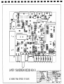
6.1.4.1 Board Silkscreen Potentiometer Identification
6.1.5. Adjusting Position Output Scale Factor and AGC Linearity
6.1.5.1. Closed Loop Method
6.1.5.2. Open Loop Method
6.1.6. Command Input Scale Adjustment
6.1.7. Oosing the Servo Loop
6.1.7.1. Class 1
6.1.7.1.1. Coarse Tuning
6.1.7.1.2. Fine Tuning
6.I.7.U. Slew Rate Limiter Speed Adjustment
6.1.7.2. Qass 0
6.1.7.2.1. Coarse Tuning
6.1.7.2.2. Fine Tuning
6.1.8. Aligning the Mirrors
6.1.9. Matching the X and Y Channels
6.2. 6740-XX Notch Filter Module
6.2.1 Background Theory
6.2.2 Notch Filter Tuning
6.2.2.1 Determining Fr
6.2.2.2 Selecting the Proper 6740-XX NFM
6.2.23 Inserting and Tuning the 6740-XX NFM
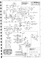
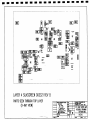
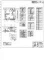
6 3 Schematics and Assembly Drawings
1.0. Introduction
As the complexity and specification requirements of today's optical systems increase, so does the
need for high performance, high accuracy, and compact mirror positioning systems. The
MicroMax™ Series 670 system was designed for applications that require high performance
specifications.
The Series 670 Single axis Board-Level Mirror Positioning System consists of a single-channel
servo amplifler on a 2.50" x 4.00" board and a high performance scanner. The scanner is
designed for a specific range of inertial loads, allowing mirrors with inertias from less than 0.001
gm-cm^ to greater than 100,000 gm-cm^ to be precisely controlled.
This manual describes the 670 servo board electronics. (A separate manual will describe the
particular motor matched to this system.) This manual describes the servo board in detail so the
user can better integrate this mirror positioning sub-system into the end use application. At the
end ofthe manual is a complete set of schematics and assembly drawings.
Please read this manual in order to fully understand the operation of this mirror positioning
system. The optical scanners used in this system are delicate devices and can be damaged if
mishandled. Do not attempt to retune the drive electronics until the tune-up procedure in section
6.0. is fully understood. Failure to do so could result in serious damage to both the scarmer and
electronics.
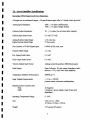
2.0. Servo/Amplifier Specifications
MicroMax 670XX Board Level Drive Electronics
All angles are in mechanical degree. All specifications apply after a 1 minute warm up period.
Analog Input Impedance:
200K + 1% ohms (Differential)
lOOK + 1% ohms (Single Ended)
Position Output Impedance:
IK + 1 % ohms (For all observation outputs)
Position Input Scale Factor:
0.5 volt/° (27volt)
Analog Position Input Range:
Digital Position Input Range:
+ 10 volts max
2'^ dac coimts
Non-Linearity of 16 Bit Digital Input:
0.006% of full scale, max
Position Offset Range:
± 1 volts
Pos. Output Scale Factor:
0.5 volt/°
Error Output Scale Factor:
0.5 \o\xr
Velocity Output Scale Factor:
Analog (scaled by position differentiator gain)
Fault Output:
Open Collector: IK ohm output impedance (pulls
down to -15V), with 10mA sink cai»bility
Temperature Stability of Electronics:
20PPMper°C
Input Voltage Requirements:
+/-15 to +/-28VDC
(current varies with motor configuration)
Maximum Drive Current Limit:
Peak:
RMS:
10 Amperes
5 Amperes (power supply, load, & heat sink
dependent.)
Operating Temperature Range:
0 -50°C
Size:
4.0inx2.inxl.06in
10.16cm X 6.35cm x 2.69cm
Weight:
3.07 oxmces (87 grams)
3.0. Description of Operation
3.1. Overview
The 670 system's servo electronics are contained on a compact 2.5" x 4.0" multi-layer printed
circuit board. Each servo board has been tuned to the customer's particular mirror inertia so that
no adjustments are necessary unless the mirror inertia is changed. For those experienced in
servo electronics, there is a tuning section included in section 6.0. Also included is a complete
set of schematic and assembly drawings.
**Waming! Do not attempt to retune the servo until section 6.0. is fully understood. Damage
to the scanner could result.
**Note: If by cmtomer request the system was sent untuned, the user will have to follow the
tuning procedures in section 6.0 before the system will be ready for use. Also, if the system was
shipped without a nurror or other customer load, the system will always be shipped untuned.
The basic operation ofthe servo is: Accept a conmiand input voltage signal and tum it into a
stable, repeatable, angular position of the scaimer's output shaft. The amplifier does this by
combining the input information with the feedback information from the scanner to form an
error signal. The servo then strives to force this error signal to zero by rotating the scanner's
shaft. It is this "following" of the input signal that allows it to contiol the scanner's angular
position.
The rest ofthe electionics on the card is used to provide DC power and to monitor various error
conditions to ensure proper operation ofthe system.
3.2. Mechanical Layout
Refer to the 670 Outline Drawing located in section 6.0. for details ofthe mechanical layout.
The 670 servo board has four clearance holes for #4 screws located at the four comers of the
board. It is recommended to use all four mounting holesTFor best noise rejection, always ground
one ofthe screw holes on the scanner cormector (J2) side ofthe board to the chassis ground of
the instrument For maximum support and heatsinking, there are two #6 holes at the left and
right extremes of the black heat-sink bracket, and two #4 holes near the middle of the bracket.
BoMt^ this side ofthe bracket to a large plate, heat sink extrusion, or machine chassis and
using thermal joint compound will greatly increase the maximum power dissipation ofthe 670
board. If this is not done, expect no more than minimal output power capability and marginal
performance imder moderate loads. It is reconmiended that all four of the heat sink bracket
fasteners be ofthe "socket head" type.
During system integration, ensure that there is sufficient clearance around and under the board to
keep the circuits firom being shorted out, and that all of the connectors, adjustment
potentiometers, and test points are accessible.
3.3. Input Power
Refer to the 670 Schematic located in section 6.0. for details on this section.
Input DC power is fed onto the board via the 4-pin male Molex connector, J3. The mating
female cormector, Molex # 15-24-4048 with Molex pins # 02-08-1202 have been included with
the system and contained in the connector kit.
The supply voltages are connected directly to the output amplifier. The voltage need not be
highly regulated, but for h i ^ accuracy applications, it is recommended the voltages be as free
from noise as practical. Filter capacitors on the 670 board help to supply the board's transient
current demandsfromthe power supplies allowing for smaller supplies in general.
The 670 board is normally used with +/- 28V supplies. The input voltage is regulated down to +/15V for the analog circuitry and +5V for the digital circuitry. The table below shows the voltage
ranges along with fault trip point levels and proper jumper and resistor settings. Consult the table
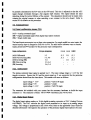
below for configuring the system with alternate supply voltages:
Supplv Voltage Range
+/-18V to +/-28v(max)
+/-15V to +/-18v(max)
Trip Point VoltaRe Jumper Connect
<+/-17v
<+/-12v
W2&W3
R94 & R96 Values
13.3k
7.87k
For operation within the +/-15v to +/-18v, the supply voltage will not be regulated on board, and
will connect directiy to the analog circuitry. In this situation, damage to the board will result if
the voltage exceeds +/-18v! For these situations, it is highly recommended that low noise,
regulated power supplies with over-voltage "crowbar" type protection be used. Refer to the next
paragraph for instruction.
In general the higher the voltage, up to +/-28V, the shorter the large angle step response time or
the better the performance. The systems are factory tested at +/-28V. The input current
requirements vary depending on a number of parameters e.g. which type of scanner is being
used, how the system is tuned, what type of waveform is being input. Power supply design
should consider the current required to run all ofthe analog circuitry, +/-150nLA, and the current
required to run the scanner at the maximiun RMS current demands.
The 670 board has power fault monitoring to ensure proper "tum-ofF' sequencing whether
intentional or accidental. Should the input supply voltage dip below a "Trip Point Voltage"
minimum set by the fault detector, the servo will tum off and stay off until the input voltage has
^
attained the proper level. Proper gauging of wire and power supply sizing should be considered
during the design integration ofthe system.
**Note: If the power supply cannot support the amount of current drawn by the servo board, the
servo board will automatically shut down. This is part of the normal "turn-off' circuitry of the
board. Do not use power supplies that "fold-back" in voltage when too much current is drawn.
This could result in a continuous fault cycling that could damage the scanner/servo combination.
Shown below is the pinout for J3 input power connector:
Pin 1 = + Supply Voltage
Pin 2 = +Supply Voltage Retiim
Pin 3 == -Supply Voltage Retum
Pin4 = -Supply Voltage
3.4. Position Demodulator
A differential current signal is obtained from the position detector within the scanner. The
amplitude of this signal is modulated by the scanner output shaft angle or "position". Referring
to tiie 670 schematic, la and lb are converted to voltages, Va and Vb, by the two transimpedance
amplifiers in the position demodulator section. The position output voltage, Vp, is then detected
as the difference of these two voltages. This signal is then sent on to the tuning section of the
amplifier and to the outside world via a buffer amplifier. This buffering allows the user to
monitor the scarmer's position without fear that the measurement device will affect the position
signal. The position signal is available at J4.2 or TPl. Use TP2 or W7.2 for the retum. The scale
factor for this output is 0.500 volt/° mechanical, standard.
3.5. AGC Circuit
The output signal of a scaimer's position detector is powered by an ACJC signal generated on the
670 board. To monitor this signal, use TP7. Use TP2 or W7.2 for the ground retum. The 670
board's ACJC circuit monitors the sum of voltages Va and Vb and forces this sum to be constant
at all times. Thus, any drift ofthe position detector is stabilized to a very high degree. Since the
angular excursion of the scanner is inversely proportional to Vagc, this circuit is also used to
adjust the position detector scale factor or the 'Tosition Output Scale Factor". However, this
should only be done when retuning the original scanner, or when matching a new scanner to the
servo board. The scaimer's scale factor should never need readjusting during its lifetime.
Changing the position output scale factor in this manner directiy affects the system's loop gain.
Tuming Rl3 to set a scanner's field size will result in changed dynamic performance. Refer to
section 6.0. for adjusting the output scale factor. ***Caution: Misadjustment of R13 could
result in damage to the scanner. Refer to section 6.0 before adjustments are made.
The apparent linearity ofthe position detector is affected by component tolerancing ofthe servo
board's position demodulator and by other factors within the scanner. These nonlinearities can
be partially eliminated by the R77 trim on the 670 board. This trim is adjusted so that the AGC
signal changes minimally through a full angular shaft rotation. This signal should not need
adjusting during the normal lifetime ofthe scanner. This adjustment should only be made when
retuning the original scanner or when matching a new scanner to the servo board. Refer to
section 6.0 for details on this procedure.
3.6. Command Input
3.6.1 Input configuration jumper fW4)
(AN) = Analog command signal
(DI) = Digital command signal (from digital input option module)
(SE) = Single ended input
The board input can accept a two or three wire connection. For single ended two-wire inputs, the
unused op-amp input is strapped to GND #6 via W4. The table below indicates were to connect
signal, ground and W4 jumpers for the particular input configuration:
Input configuration
(AN) Differential
(AN) Non-inverting (SE)
(AN) Inverting (SE)
(DI) Non-inverting
(DI) Inverting
W4 pin strapping
1-3
1-3,4-6
3-4
3-5,4-6
5-6,3-4
r+)in (-)in GND
J1.3
J1.3
-
Jl.l
Jl.l
J1.2
J1.2
J1.2
3.6.2. Analoe Input
The analog command input signal is applied via Jl. The input voltage range is +/-10V for fiill
angular excursion. Ensure that W4 and the input signal on Jl are connected for the particular
configuration desiredfromthe chart above. The scanner will move as follows:
input voltage = -lOV
input voltage = OV
input voltage = +10V
position = full CCW angle
position = center
position = full CW angle
The coimector kit included with your system has the necessary hardware to build the input
connector J1. The connector is Molex #50-57-9404 witii Molex pins # 16-02-0103.
3.63. Digital Inpot Module
The digital input option employs a 16-bit digital-to-analog converter or DAC (Analog Devices
#AD7846JP). The DAC converts the digital word presented at its input to an analog output
voltage. This voltage is proportional to the 16-bit word. Refer to the applicable Users Guide for
detailed information with regard to the operation ofthe particular digital input option to be used.
3.6.4. Command Input Scale Factor Calculation
The Command Input scale factor is defmed as the nimiber of volts required at the input of the
servo board to cause the scanner's output shaft to rotate one mechanical degree. For some
applications, fine control of this scale factor is critical. Also, since the input voltage is limited to
+/-10V, this also sets the maximum contiollable angle or Input Range ofthe system. This Input
Range is also referred to as the "fieldsize" ofthe system.
The 670 Single Axis Mirtor Positioning System is normally set up for the maximum allowable
scan angle for the application unless otherwise specified by the customer. The maximum
fieldsize for all Cambridge Technology scanners is +/-20° mechanical. As the Conmiand Input
scale factor increases, the inherent fieldsize ofthe system decreases. Thus, 0.5V/° system will
yield +/-20°, 1.0V/° will yield +/-10°, 2.0V/° will yield +/-5°, etc.
Note: It is possible to set the scale factor less than 0.5V/°, however it will allow the input signal
to attempt to drive the scanner further than 20°. This will cause the system to sense the
overposition and shut the servo down. Ensure that no matter what the servo's input scale factor
is set to, the input signal stays within the bounds that keep the scanner within its normal +/-20°
range.
The Command Input scale factor is coirtrolled by the following factors:
1.)
2.)
3.)
4.)
Position Output Scale Factor - always set to 0.5V/° mechanical (unless otherwise stated)
Error integrator summing resistor ratio, R29/R30 - usually set to 1:1
Slew rate limiter voltage gain, R89/R83 - usually set to 1.074:1
Command Input scale adjustment, R51 & R82 - adjustable from ~0.8:1 to 1:1
**Note: The R51 and R82 combination allows the user to make small adjustments to the
Command Input scale factor. For gross changes use the equations shown below to determine the
value of R30. For small changes, use R51. For minimum drift from R51, set the pot to the
maximum CW position. Then use the procedure in section 6.0 to measure the input scale factor
obtained.
The following equation describes the interaction ofthe above factors:
Command Input Scale Factor = Position Output Scale Factor x (R30/R29) x Slew Rate Limiter
Voltage Gain x Command Input Scale Adjustment
For example: Let
Position Ou^ut Scale Factor = 0.5 V/*' mechanical
Slew Rate Limiter Voltage Gain = 1.074:1
Command Input Scale Adjustment = 0.9311:1
R29=10Kohm
10
and the desired Command Input Scale Factor = 2:1 or 1.0V/° mechanical
Thus,
R30 = (Command Input Scale Factor * R29) / (Position Output Scale Factor x Slew Rate
Limiter Voltage (jain x Command Input Scale
Adjustment)
or
R30 = (l.OV/^ mechanical • lOKohm) / (0.5Vr mechanical x 1.074 x 0.9311)
R30 = 20Kohm (Use a high quality metal film resistor, RN55C, for best thermal drift
characteristics.)
The Command Input Range or "Fieldsize" is now determined as the product ofthe range ofthe
Command Input voltage and the Command Input scale factor. For the above example:
Command Input Range = +/-10V * 1.0V/° mechanical
Command Input Range = +/-10° mechanical = 20° mechanical pk-pk
A detailed procedure is included in the appendix 6.0 on how to set the Command Input Scale
Adjustment Basically, R51 is adjusted so that the proper voltage ratio is measured from W4 to
the position output voltage measured on TPl.
3.6.5. Command Offset
The Command Offset is used to add a small DC offset for a specific application requiring it.
Two methods are available on the 670 board. The first is an on-board adjustment pot, Rl. Rl is a
15-tum Cermet potentiometer whose output voltage ranges from -5V to +5V. Its offsetting
contribution is contiolled by RIO. The nominal offset contribution is +/-20% ofthe input range.
The second Command Offset input is accepted via the 4-pin Molex C-grid coimector J 1.4. Use
J 1.2 for the retum. This is a high impedance input with a +/-10V range. Its contribution is
conti-olledbyR85.
**Note: When the extemal Command Offset input is not intended to be used, do not install R85.
If R85 has been installed, but J1.4 is not connected to a low impedance signal source, short J1.4
to J1.2. Otherwise, a large unintended offset voltage will be added to the command input.
3.6.6. Command OfTset Scale Factor Calculation
Since there are two Command Offset inputs, there are two Command Offset Input Scale Factors
to describe.
11
The command input offset adjustment potentiometer, Rl, confrols a DC input signal that is
added to the normal input signal. RIO confrols the contribution of this input. The following
equation can be used to determines the value of RIO for a desired Command Offset Range:
RIO = (((+Vr) - (-Vr)) x R89 x (R29/R30)) / (Position Output Scale Factor x Command Offset
Range)
if
Vr = 5V
R89 = lOKohms
R29 = lOKohms
R30 = 20Kohms
Position Output Scale Factor = 0.5V f mechanical
Command Offset Range = 0.25° mechanical
tiien RIO = (lOV x lOKohms x (10K/20K)) / (0.5V/° mechanical x 0.25° mechanical)
RIO = 400Kohms
The other type of Command Offset is brought in from an extemal source similar to the normal
input. This input can be used while simultaneously using the analog or digital input. The
resultant signal is the algebraic sum of both. The following equation is used to determine the
value of R85 in order to obtain the proper Command Offset Range:
R85 = ((+Offset In - -Offset In) x R89 x (R29/R30)) / (Position Output Scale Factor x Position
I
Offset Range)
if
Offset In = lOV
R89 = lOKohms i
R29 = lOKohms
R30 = 20Kohms
Position Output Scale Factor = 0.5 V/° mechanical
Command Offset Range = 0.25° mechanical
tiien R85 = (20V x lOKohms x (10Ky20K))/(0.5V/*'mechanical x 0.25° mechanical)
R85 = 800Kohms
**Note: For best drift characteristics, select a Command Offset Range that is fairly small
compared to the Input Range ofthe system.
**Note: The algebraic sum of all inputs must not exceed +/-20° mechanical or the system will
go into "fault" mode. This is described in detail in section 3.9.
3.6.7. Slew Rate Limiter
All ofthe Command Input signals, wiiether analog, digital, or offset, must pass through the "slew
rate limiter". The slew rate limiter is a circuit used for confrolling the system for large angle
moves. During these moves, large currents are drawn by the servo's output amplifier. If these
12
exceed the capability of the power supply or the board's output amplifier, noise and even
instability can result. By controlling the maximum slew rate of the input signal, the system's
output amplifier can be kept from saturating. This is always advantageous for accurate
positioning of the scanner. For some applications, fast large-angle positioning is not needed.
For those applications, the slew rate limiter can be used to slow the maximum angular speed
attained for these large moves, thus decreasing the amount of wobble and jitter associated.
The slew rate limit is contiolled by R78. Refer to section 6.0 for adjusting the slew rate limiter.
••Note: During start up, the output of the slew rate limiter is grounded by the action of an
analog switch, U15B, for about 3 seconds. This allows the servo time to stabilize (about 1
second).
**Caution: Do not adjust R78 without complete understanding of the appropriate section of
6.0. Damage to the scanner could result.
3.7. Tuning Section
The tuning section can be configured two ways depending on the user's needs. If extieme
positioning repeatability is required, the servo board is set up as a class 1 servo. If fast
positioning is of paramoimt importance, the servo board has class 0 capabilities.
The class of servo is determined by how many error integrators are in the servo loop. The error
integrator of a class 1 servo makes the system settle to a very high degree of accuracy. Even as
friction or other torque disturbances try to affect repeatability, the integrator will eventually take
out all error. This is done at a slight speed penalty. Most applications' requirements are met
very well using the class 1 servo.
Class 0 servos are slightiy faster and more stable than class 1 servos. However, the tradeoff is that
any finite friction causes a vWndow of non-repeatability to form around the commanded position.
The error is equal to:
Ertor = F D / K S
where. Error = difference between actual and
commanded position in radians
FD = the disturbance torque in dyne-cm
Ks = the servos stiffness in dyne-cm/radian
Certain applications do allow for the use of the class 0 configuration, along Avith its inherent
non-repeatability. It is described below after the class 1 section.
13
3.7.1. Class 1
Our class 1 servo consists of the following circuits: position differentiator, position amplifier,
error integrator, current integrator, and summing amplifier. The ttansfer fimction can be
characterized by the following differential equation:
V(t) = Al • d rVpos(t)) + A2 • Vpos(t) + A3 • jError(t)dt + A4 • Jl(t)dt
dt
where:
V(t) = output of summing amplifier
Al - A4 = coefficients that are adjusted with the tuning pots R25, R28, R31, and R59
respectively.
Error(t) = the error signal generated as the difference between the position signal, Vp, and the
output ofthe slew rate limiter (command signal).
I(t) = the currentflowingthrough the motor coil.
The position differentiator takes the first derivative of the position signal to yield angular
velocity. This velocity signal is one of two sources of damping for the servo. Its -3db bandwidth
is set relatively low This is to prevent highfrequencynoise, present on any differentiated signal,
from entering the summing amplifier. Its contribution to the servo is to provide damping at low
frequency and is contiolled by R25.
The position amplifier uses the position signal to generate an "electrical spring". Its contribution
is contiolled with R28.
The error integrator compares the actual position to the commanded position and integrates the
difference over time. This signal will allow the scanner to overcome any slight spring or friction
yielding a zero steady-state ertor. Extiemely repeatable positioning is thus obtained. The
ultimate accuracy is then contiolled by the repeatability ofthe position detector contained within
the scanner. The contribution of this amplifier to the servo response is contiolled by R31.
The current integrator produces a signal proportional to the integral of the cmrent flowing
through the rotor. Since the current flowing through the rotor is proportional to the torque
produced, it is also proportional to the angular acceleration. Thus, the integral of ciurent can be
used as another source of velocity information, hence damping. The advantage of this form of
damping is its inherent low noise. Its bandwidth can be set high without degrading its signal-tonoise ratio. The overall bandwidth of the system can be extended much fiirther than with
position differentiation alone. The current integrator is considered the high frequency damping
source and is adjusted with R59. The current integrator is high-passed into the summing amp by
way of R107, R60, and C9.
14
The summing amplifier algebraically sums all four of these signals to obtain a composite signal
that is sent to the output stage. During startup, a FET, Ql is tumed on slowly so that the servo
has time to stabilize in a contiolled manner. Also, when an ertor condition is sensed, an analog
switch, U15C, is shorted across this amplifier, thereby opening the loop and shorting the signal
being sent to the output stage to ground. During mirror alignment the gain of the summing
amplifier is reduced by two orders of magnitude which drastically lowers the loop gain. This
allows the customer to align the mirror manually without the servo going unstable. This is
explainedfiirtherin the mirtor alignment section in appendix 6.0.
3.7.2. Class 0
Our class 0 servo consists of the following circuits: a position differentiator, an error amplifier,
a cmrent integrator, and a summing amplifier. The tiansfer fimction can be characterized by the
following differential equation:
V(t) = Al • d (Vpos(t)) + A2 • Error(t) + A3 • J I(t)dt
dt
where:
V(t) = output of summing amplifier
Al - A3 = coefficients that are adjusted with the tuning pots R25, R28, and R59.
Error(t) = the error signal generated as the difference between the position signal, Vp, and the
output ofthe slew rate limiter (command signal).
I(t) = the currentflowingthrough the rotor coil.
The position differentiator takes the first derivative of the position signal to yield angular
velocity. This velocity signal is one of two sources of damping for the servo. Its -3db bandwidth
is set relatively low. This is to prevent high frequency noise, present on any differentiated
signal, from entering the summing amplifier. Its contribution to the servo is to provide damping
at low fi^uency and is contiolled by R25.
The error amplifier compares the actual position to the commanded position and generates a
signal proportional to this error. Since this is not an integrated signal, the bandwidth of this
stage is much higher. Thus, the closed-loop bandwidth of the servo is also higher. The sacrifice
is that if there is any fiiction or spring present, there will be some DC error. However, since
Cambridge Technology's scanners have very low friction and no torsion bar, this error is quite
small. The contribution of this amplifier to the servo response is contiolled by R28.
The current integrator produces a signal proportional to the integral of the current flowing
through the rotor. Since the current flowing through the rotor is proportional to the torque
produced, it is also proportional to the angular acceleration. Thus, the integral of current can be
15
used as another source of velocity information, hence damping. The advantage of this form of
damping is its inherent low noise. Its bandwidth can be set high without degrading its signal to
noise ratio. The overall bandwidth of the system can be extended much ftuther than with
position differentiation alone. The current integrator is considered the high frequency damping
source and is adjusted with R59.
The summing amplifier algebraically sums all four of these signals to obtain a composite signal
that is sent to the output stage. During startup, a FET, Ql is tumed on slowly so that the servo
has time to stabilize in a contiolled manner. Also, when an error condition is sensed, an analog
switch, U7, is shorted across this amplifier, thereby opening the loop and shorting the signal
being sent to the output stage to ground. During mirror alignment the gain of the summing
amplifier is reduced by two orders of magnitude v^ch drastically lowers the loop gain. This
allows the user to align the minor manually without the servo going unstable. This is explained
further in the mirror alignment section in appendix 6.0.
3.8. Output Amplifier
3.8.1 Overview
The output stage uses a power op-amp to supply the large currents used to create torque in the
motor coil. A current feedback loop is tied around this output amplifier allowing the summing
amp to contiol the current in the scanner directiy. Thus changes in cable length, coil resistance,
contact resistance, back EMF voltages, etc. do not affect the summing amplifier's ability to
control the torque produced in the scanner. This produces a very stable and repeatable system
response with time and temperature.
Current flowing through the motor coil is detected by a low resistance current shunt, R52 and
differentially detected by the current monitor U4D. The current monitor signal is then used to
close the current feedback loop around the output op-amp U5. It is also used for the "coil
temperature calculator" to monitor coil heating and by the current integrator to obtain a velocity
signal. The current monitor signal is monitored on TP3. Use TP2 or W7.2 for the ground
reference. The current monitor gain varies depending on which scanner is being driven. Check
the scanner data sheet for the maximum rms current the scanner can maintain.
The bandwidth ofthe output stage is mainly contiolled with a lead in the current feedback loop.
The series/parallel combination of R50 and C8 and R49 in the cmrent monitor's feedback path
provides this lead. This RC combination is set so that the output current waveform is adequately
damped when a square wave is fed in. Secondary bandwidth limiting is provided via the "noise
gain" compensation technique with R40. For large mirror loads, a notch filter module is used to
stabilize large inertia systems that tend to "sing" or resonate at the system's torsional resonant
frequency. See section 6.2 for more information regarding Notch Filters.
16
3.8.2. Output Stage Disable
The output amplifier is disabled during the power up sequence and recovery from a fault
condition. See sections 3.11 and 3.13 for details. The output amp can also be manually disabled
by grounding the TP4 "MUTE" test-point, or the Remote Shutdown input on J4.6. Grounding the
Remote Shutdown input will disable the output amp by initiating a continuous fault recovery
sequence, but grounding TP4 will not. Therefore, TP4 is useful for performing Notch Filter
Module tuning (see section 6.2).
For added motor protection a fuse Fl has been placed in-line with the output op-amp U5. See
the motor specifications for the proper fuse rating to be used with each servo configuration. To
momtor the voltage signal being sent to the scanner, clip a scope probe to one side ofthe fiise.
Use TP2 or W7.2 for the ground reference.
3.9. Reference Voltages
A voltage reference, U17 (LT1021-5), provides +5 volts for the overposition monitor. Command
Offset contiol, coil temperature calculator, and the DAC references. It is also converted to -5
volts through an inverting amplifier, U16B. The -5 volts is used in the ACJC circuit, overposition
monitor, and the DAC references. The +/-5 volts used for these various functions are labeled +/VREF, so that they are not confused with the +5 volts used to power the digital circuitry. The
two reference voltages are available on W7.1 (+VREF) and W7.3 (-VREF) for extemal use
provided that no more than 2ma current is drawn from either of them. W7.2 is the ground
reference for these voltages.
3.10. Notch Filter Socket
The 670 Board is ready to accept a 6740-XX series Notch Filter Module (NFM). This module is
inserted into the J5 socket. If the NFM is not used, then pins 1 & 2 ofthe socket must be shorted
together. See appendix 6.2 for infoimation regarding the use ofthe 6740-XX NFM.
3.11. Observation/Control Header
3.11.1 User Outputs
Various observation and contiol signals exist on J4. They are listed below:
J4.1 - Velocity out
Time derivative of position out signal (IK ohm output impedance).
Velocity Out = (5Vpos(t)/8t)^R100^C33
J4.2 - Position out
Position out signal (IK ohm output impedance). Position Out = Vpos(t)
17
J43-GND#2
(jroimd retum of bypass capacitors.
J4.4 - Error out
Must have a shorting jumper on W9 1&2 for class 1, W9 2&3 for class 0.
Class 0
Class 1
Error(t) = Vcom(t) - Vpos(t) Error(t) = (R105^C7/C16)^ {Vcom(t)/R30 - Vpos(t)/R29}
J4.5-GND#4
(jround retum of digital circuits.
J4.6 - 90% max power flag
This is an open collector switch that pulls down to -15v when within 10% of a coil
temperature fault shutdown (IK ohm output impedance, lOma sink capability).
J4.7 - Fault out
This is an open collector switch that pulls down to -15v when the fault detector circuit
trips (IK ohm output impedance, lOma sink capability).
J4.8 - Remote Shutdown input
This input causes the servo to enter a fault mode when grounded.
3.11.2 Remote Shutdown Input
If it is desired to stop tiie scanner automatically, tiie "REMOTE SHUTDOWN" input on J4.8
allows the user to do so. This signal disables the output amp and trips the fault detector, when
grounded, which stops all scanning action within milliseconds. To shut down the servo, use an
open-collector fransistor switch capable of sinking at least Ima to ground J4.8. The fransistor
should have a minimum WCE breakdown rating of 20v. Use J4.5 as the ground reference. The
LED status indicator will be orange during remote shutdown.
**Warning!! During shutdown the scanner's position may be anyv^ere within -120° optical.
If the board's "fault out" signal is not used to control the laser power or direction, the laser may
point in an inappropriate direction ^^^en the scanners are shutdown.
When the Remote Shutdown signal is de-activated, the board cycles through a normal tum-on
sequence as described above.
3.12. LED Status Indicator
The LED status indicator will visually describe the three states ofthe servo system as followrs:
Green: system is in Normal operation mode.
Red:
system is in Fault mode.
Orange: system is in Remote Shutdown mode.
18
3.13. Protection Circuits
The 670 board has various protection features, some of wiiich have been mentioned above. The
primary purpose of this circuitry is to allow the servo to stabilize in a contiolled fashion during
startup, and to shut down the scanner in a confrolled maimer should it detect any error conditions
that could damage the scanner.
The 670 system has two output signals that allow the user to monitor system status. One is the
"FAULT OUT" signal available on the J4.7, and tiie otiier is the "90% Max Power Warning"
signal available on J4.6. Use J4.5 for the ground retum. These are open collector switches that
pull down to -15v when active, and have a IK ohm output impedance. The ciurent sinking
capability of these outputs is lOma. The LED Status Indicator on the board tums red whenever
the board is in the fault condition.
3.13.1. Startup Sequence
During a normal startup the fault detector U8 goes into an error or "fault" state. This causes the
following:
1. The output amp is disabled via U15A, effectively disconnecting the scanner coil from the
servo amp.
2. The summing amplifier gain is reduced by a factor of 100 via U15C and R35, allowing a
very small ertor signal to be sent to the output stage.
3. The "command in" signal is disabled via U15B, reducing the command input to zero.
4. The "fault out" signal on J4.7 is active, and the LED status indicator glows red.
After 1 second, the first stage of U8 resets and following actions occur:
1. The output amp is enabled, allowing current from the output stage to pass through scanner.
2. The summing amplifier is enabled and the FET across it tums off slowly so that the gain
in the summing amplifier slowly increases.
3. The "command in" signal is still disabled.
4. The above actions cause the scanner to center itself in a contiolled way, but prevents the
scannerfrombeing driven v^diile doing so.
5. The "fault out" signal stays active with the status LED red.
19
After 2 additional seconds (3 seconds from tum-on), the second stage of U8 resets and the
following actions occur:
1. The error integrator is enabled via U15D.
2. The "position in" signal is enabled.
3. The scanner will begin to follow the input signal.
4. The "fault out" signal de-activates and the LED tums green.
3.13.2. Error Shutdown
There are several error states that the protection circuitiy is designed to detect and guard against.
They are:
1. Loss of position detector signal: If the cable is not plugged into the scanner or the servo, or if
there is a loss of position detector signal for any reason, the fault detector will see this. Va
and Vb have to be above a minimum voltage of 0.96 volts.
2. Position Signal. VP has exceeded +/- 10 volts: There are intemal mechanical stops within
the scanner that prevent it from spinning a fiill 360°., however during a fault state, the current
must be shut off before the rotor reaches these intemal stops. The electionics are set to sense
when the scanner has exceeded the maximum legal range, +/-20° mechanical. This is
accomplished by comparing the position signal (reduced by a factor of two) to the +VREF
and the -VREF levels. If Vpos exceeds either one, the fault detector will sense this overposition and trip. Thus, the position output signal must be kept within +/-10 volts or the
servo will fault. On systems whose fieldsize has been set to +/-20° mech., the system may
trip whenever the edge of the field is approached (65535 and 0). Caution! Do not let the
system stay in this condition indefinitely. The scanner might be damaged.
3. Over-temperature: The coil temperature must be monitored at all times when the scanner is
being operated close to its performance limit. On the 670 board this is accomplished by the
"Coil Temperature Calculator" circuit. This circuit rectifies the current signal, then performs
an I^/R calculation to determine the power dissipated in the coil. Then, loiowing its thermal
time constant and thermal conductivity to the case, the temperature can be calculated. The
"90% Max Power Warning" output signal on J4.6 will be activated when within 10% of
tripping the fault detector. The fault detector will trip and the "fault out" signal on J4.7 will
activate whenever the coil temperature reaches its maximum safe operating limit.
4. Loss of power: To ensure protection during "brown-outs", the servo will shut the system
down if the Input Power Voltages drop below a preset minimum. During system integration,
ensure that the power supplies and the power supply connections can meet the demands of
the scanner operated at the performance levels expected for the application. If not, the input
voltage will dip, and fault circuitry will activate. This can cause a fault "cycling" to occur.
20
Do not operate the system under these condition or damage to the scanner may occur. See
section 3.2. "Input Power" for a more detailed discussion on this.
3.12. Mirror Alignment Mode
The mirror alignment mode shunt is W5. It allows the user to loosen the mirtor screws, align the
mirrors, and retighten the mirror screws, without the system going unstable. It does this by
lowering the loop gain of the system. When W5 is shorting pins 2 and 3, the system is in the
normal operating mode. When the jumper is between pins 1 and 2, the system will center itself
and feel somewhat "limp" compared to normal operation. The scanner will not follow any input
signals when in class 1 mode.
••Caution!! If the system is set up for class 0 operation, the scanners will still follow the input
signal, but at a much reduced loop gain. Do not operate the scanner in this mode except to align
the mirtors. Damage to the system could result and void the warranty. Refer to the tuning
procedure in section 6.0 for the mirror alignment procedure.
21
4.0. Operating Instructions
4.1. Precautions and Warnings
As a standard practice, keep the servo channel, scanner, and mirror together as a matched set. At
Cambridge Technology, we have matched all three components and tested them as a system.
Mixing and matching systems invalidates all of the calibrations that have been done. If mixing
the systems is unavoidable, please follow the entire tuning procedure in section 6.0. to verify
proper operation. Failure to do so could degrade the performance of the system or possibly
damagetiiesystem.
Always make sure the scanner is heatsinked properly before operating it for any length of time.
Failure to do so can cause a scanner failure due to overheating. Follow the mounting procedures
covered in the scanner's Instmction Manual.
Do not attempt to tum any of the servo adjustment potentiometers on the servo board until the
entire tune-up procedure has been read and fully understood! The error protection circuitry may
not work if the servo was improperiy adjusted, causing damage to the scanner.
The Series 670 Single Axis Mirror Positioning System is a high performance servo/scanner
system that requires delicate handling. Do not drop or mishandle the scanner, or damage may
result.
Do not operate a scanner without its mirror, or other appropriate load, attached securely to the
output shaft (except during mirtor alignment). Always ensure the mirror is pushed all the way
onto the scanner shaft beforetightening.Do not use anything other than medium finger pressure
to install a mirror mount onto the shafl Always tighten the mirror mount screws tightly before
switching the system back to normal mode. Operating the scanner without a load may cause the
system to go unstable, possibly causing damage to the scanner. Do not change the mirrors in any
CTI system without checking the tuning afterwards. The ultimate performance of the system
will be greatly reduced.
When operating the system, do not repeatedly slam the scanner into its overposition limits at +/20° mechanical. Although the protection circuitry shuts the scanner down effectively, the
momentum of the rotor and load will still carry the rotor into the mechanical stop. If done
repeatedly, the scanner could be damaged.
If the system was ordered without mirrors, the electionics and scanner are tested with test loads,
then the servo is "detuned" as outlined in this procedure. These systems must be retimed by the
customer before the system can be operated normally. Please refer to section 6.0. for tuning
information.
22
4.2. First Time Startup
1. Using the connector kit provided with your system, make the connectors for Jl and J3 as
appropriate. Do not attach them to the 670 board at this time. After constracting the cables,
double-check the wiring to ensure that everything is correct. Applying voltages to the wrong
inputs would probably damage the scanner and the servo board which would void the
warranty. Check the input power section, 3.3.
2. Check that the jumper configuration of W2 and W3 are correct for the voltages provided at
the power supply inputs. Check the input power section, 3.3.
3. Plug the scanner cable, male end, into J2 on the servo board and tighten the locking screws
securely.
4. Plug the scanner cable female end into the connector on the scanner and tighten the locking
screws securely.
Note: Step 5 is for systems that do not already have the mirrors mounted and aligned.
5. Install the mirror on the shaft ofthe scanner and tighten securely. Ensure that the mirror's
angular swing does not allow it to hit any obstmction (e.g. the table the scanner is sitting on
or each other). Also ensure the mirror alignment mode jumper W5 is shorting pins 2 and 3.
(Not in alignment mode.)
6. Ensure that power is not being applied to the input power coimector, J3 and attach it to the
670 board.
7. If the system is to be driven from an analog input, install the Jl connector as appropriate. If
the system is digital, refer to the applicable document for the digital input option used.
Ensure W4 is set appropriate for the type of input. Whichever type input is being used, set
the input signal so the scanner centers. For analog inputs this is 0.000 volts. For the digital
inputs, set them to 32768 lo. For more information, see the Command Input section 3.6.
8. Tum the power on and observe the scanner shaft. One second after tum-on, the shaft should
tum to the centered position. Three seconds after tum-on the scanner will move to the
commanded position, which also should be centered for now.
9. Turn the mirror load by the edges verv lightiy to observe if the servo has "stiffened up.
"Stiffening up occurs when the scanner is under proper servo contiol. The scanner should
resist your lijght efforts to tum it Do not be alarmed if a whining sound is heard or slight
clicking is felt when this attempted. This is the normal operation of the current integrator
and can be ignored. These sounds will not be made during normal operation.
10. Hook up an oscilloscope or other voltage meter to the Vp signal at TPl. At this time the
voltage should read very nearly 0.0 volts. Use TP2 or W7.2 for the ground reference.
23
11. For digital signals, input a 30 Hz square wave that spans about 5% ofthe field. For analog
inputs, put in a square wave of about IV p-p at about 30Hz. For very large scanner/mirror
systems, 30Hz may be too fast. For those systems, set thefrequencyto ~5Hz.
12. The scanner should immediately start moving in response to this input. Check the position
out signal or look at the scanner itself and observe that it responds appropriately to the input
signal.
13. Gradually, increase the amplitude ofthe input signal until the Command Input waveform has
almost reached ~+/-10 volts. For systems that have an input and output scale factor = 0.5
volts/° mechanical, the scanner will just go into shutdown at this point. The amplitude will
have to be tumed down slightly in order to recover. Don't continuously test this over position
shutdown feature because the scanner is stiessed unnecessarily.
14. Now, gradually tum up thefrequencyofthe input waveform until the desiredfrequencyhas
been reached or the output waveform begins attenuating, whichever comes first. The
maximum coil temperature may be reached before this point. To recover, tum the frequency
down and possibly the amplitude ofthe input signal, in that order.
15. If appropriate, enter an offset signal into the "Offset In" input. The output waveform should
now be the algebraic sum of both the normal and offset inputs.
That is it! If the 670 system has performed all ofthe above functions, it is functioning properly.
The scanner can be made to follow any input waveform as long as the maximum
amplitude/maximum speed limitations are not exceeded.
24
5.0. Limited Warranty
CTI warrants that its products will be free of defects in material and workmanship for a period of
one year from the date of shipment. CTI will repair or replace at its expense defective products
retumed by the Customer under a Retum Authorization number issued by CTI. This warranty is
void if the product is damaged by "misuse" or "mishandling" by any party not under the contiol
of CTI. Misuse or mishandling will be determined by CTI. Misuse includes use of CTI product
with incompatible products resulting in damage to the CTI product. The customer is responsible
for charges for retuming product for repairs. CTI is responsible for charges for shipping product
repaired under warranty back to the customer when CTI is allowed to choose the carrier and
level of service. The Customer is responsible for repair charges and all shipping charges for nonwarranty repairs. CTI's sole liability for any use of its product, regardless of the operating
condition of such product, is limited to repair or replacement ofthe product. The Customer holds
harmless and indemnifies CTI from any and all other claims resulting from the use of CTI
products.
25
6.0. Appendices
6.1. Tnne-up procedure
6.1.1. Precautions
Read the following procedure completely before attempting to retune the system. Serious
damage to the scanner could result if the servo were improperly adjusted!
**Caution!! Shut the system down immediately if a resonance occurs. A resonating scanner
will make a load noise that sounds like a buzzer or possibly like a highfrequencywhine. Do not
confuse this with the normal sound the scanner makes while operating. If this occurs while
tuning up the system, shut it down immediately. Check to make sure the mirror load is correct
for the scanner and is firmly attached. If so, start the tuning procedure over again. This is the
only way to ensure the scanner isn't damaged. Contact Cambridge Technology if a resonance
condition cannot be resolved.
6.1.2 Overview
For most users, the factory settings on the 670 board will never need adjusting. However, if the
user wants to change the mirror load originally used, the system will probably have to be
retimed. This procedure is aimed at the user who has an electionics background dealing with
servo contiolled systems. Do not attempt this procedure if any part of it is not clearly understood.
This procedure explains all of the adjustments that are performed at Cambridge Technology.
These include the Notch Filter, Position Output Scale Factor, the AGC Linearity, the Command
Input Offset, the Command Input Scale Factor, Closing the Servo Loop, and the Slew Rate
Limiter.
The following procedure can be used to tune-up the system completely, or to just "touch up" or
verify any one of the adjustments. If the tuning adjustments are to be just verified and/or
touched up, do not initialize the tuning pots as it states for a complete tune-up. Otherwise the
customer will be forced to perform unnecessary steps, which could possibly reduce the
performance of the system, depending on the experience of the adjuster. Call Cambridge
Technology if any parts of this procedure are not completely understood.
**Caution!! Failure to carefully monitor the scanner's position response while adjusting the
servo trimpots could result in an uncontiolled resonance which could damage the scanner.
6.1.2.1 The order in which the adjustments should be made are:
1)
2)
3)
4)
5)
Notch Filter Frequency adjustment (sec 6.2)
Command Input and Position Output Scale Factors, Linearity (sec. 6.1.5,6.1.6)
Closing the Servo Loop (sec 6.1.7)
Slew Rate Limiter adjustment (sec 6.1.7.13)
Matching X and Y Servo Channels (sec 6.1.9)
26
Once the scanner is tuned up, there is a procedure in section 6.1.9 that explains how to match the
responses of two servo axis channels. For best X-Y scanner performance for most applications,
the responses of both channels should be matched.
6.1.3. Required Tools and Materials
1.
2.
3.
4.
5.
Dual tiace oscilloscope.
Function generator - needs to have a sine and square wave output.
Digital voltmeter
Hand tools -jeweler's screwdriver flat-tip
Clip lead with "micrograbber" ends.
6.1.4. Initial setup
Ensure the power is tumed off prior to performing the following steps.
1. Refer to the startup procedure in section 4.2. above. Follow steps 1 -7.
2. To find the location of the test points and the tuning potentiometers or '^mpots", refer to
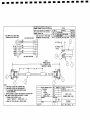
the Outiine Drawing, D03457, located in section 6.2.
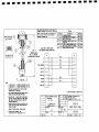
6.1.4.1. Board Silkscreen Potentiometer Identification
The tuning, scale adjustment, position offset, and linearity potentiometers are indicated with a
silkscreen aligned under the respective potentiometer on the bottom of the 670 board. The
identification is as follows (left torighton underside of board):
Silkscreen
, PS
LIN
SRL
IS
PO
EI
LFD
SG
HFD
BW
Ref Des Description of Potentiometer Function
R13
Position Scale adjustinent
R77
Lineanty adjustinent
R78
Slew Rate Limiter adjustment
R51
Input Scale adjustinent
Rl
Position Offset adjustment
R31
Error Integrator coefficient adjustment
R25
Low Frequency Damping coefficient adjustment. Also
referred to as "Position Differentiator".
R28
Servo Gain coefficient adjustment Also referred to as
"Ertor Amplifier".
R59
High Frequency Damping coefficient adjustment. Also
referted to as "Current Integrator".
R107
Band Width adjustment tor HFD and LFD alignment
27
6.1.5. Adjusting the Position Output Scale Factor and the AGC Linearity
The Position Output Scale Factor is precisely adjusted at Cambridge Technology and under
normal circumstances never needs adjusting by the customer for the life of the servo board or
scanner. If however the customer has changed the scanner originally sent with the servo board,
(remember they are matched sets) use the following procedure to verify/adjust this signal.
The most important signal generated on the 670 board is the Position Output, Vp, signal. In
order for the servo and the error protection circuitry to work correctly, the Vp signal must be
scaled properly. The Position Output Scale Factor is conttolled by increasing or decreasing the
AGC voltage sent to the scanner's position detector. The Position Output Scale Factor is linearly
proportional to this AGC voltage. Thus, changes in the Position Output Scale Factor causes
changes in the amount the scanner will move for a given output response from Vp. R13 is used
to adjust this AGC signal. This trimpot allows-10% adjustment range. If the AGC voltage is
changed by more than 1% during this adjustment, the tuning ofthe system must be verified to be
sure that it is still set properly. It is always pmdent to check the tuning after any adjustment to
the Position Output Scale Factor or the Linearity Adjustment.
The Linearity Adjustment is used to improve the linearity of the position detector and position
demodulator. By varying the amount that Va and Vb sums together to create the AGC voltage,
the linearity is improved. The intention of this adjustment is to minimize the amount the AGC
voltage varies as a function of the angular position of the scanner. Since the Linearity
Adjustment and the Position Output Scale Factor adjustments affect each other, they must both
be set at the same time.
Note: Do not allow the AGC signal present at TP7 to exceed 11 volts or the AGC circuit may
saturate, which would result in improper operation.
••Caution: In all cases, the position signal, Vp, must always have the ability to exceed +/-10
volts when the scanner shaft is tumed to its intemal mechanical stops or scanner damage may
occur.
6.1.5.1 Closed Loop Method
If the system is afready tuned up and verification or "touching up" of the Position Output Scale
Factor and Linearity Adjustment are desired, use of this method is allowed. Also, if mixing and
matching scanners, this method can be used. A mirror must be mounted on the scanner shaft, or
some other means of measuring the scanner's angular position must be employed. By reflecting a
laser beam from the mirror to a wall, and using some simple trigonometry, the Position Output
Scale Factor can be adjusted with high resolution. The further from the wall, the more accurate
this method.
1. Follow steps 1 - 7 in section 4.2. above. Set up the input for analog single ended operation
by setting Jl and W4 as indicated in section 3.6.
28
2. Tum on the power.
3. The system should perform its normal tum-on process as described in section 4.2. above.
4. Adjust the Command Input Offset Adjustment trimpot, Rl to 0.000 volts as measured on
R1.2 (wiper). Use TP2 or W7.2 as the ground reference. Center the scanner by inputting a
signal into the Command Input so that Position Output voltage reads 0.000 volts as measured
at TPl.
5. Reflect a laser beam onto the mirror of the scanner being adjusted. This laser beam should
be parallel to the wall and level to the floor before it strikes the mirror on the scanner.
Position the scanner body vertically and so that the beam is striking the wall perpendicularly.
The scanned beam should be in the same plane as the beam striking the mirror. This is
important so that the optical beam deflection angle to mechanical deflection angle
relationship is a constant factor of two. Compound angles result in relationships that are not
just a factor of two. Mark tiiis location on the wall and label it PI. Measure the length from
the mirror to the wall and call this distance Ll.
6. Input a sine wave signal that drives the scanner to half of the full peak-to-peak angular
swing. Usually an input amplitude of 3.535 volts rms is appropriate. See section 3.6 above
for more information on the input scale factor calculation. Use an inputfrequencyof-30 Hz
for most applications. For systems with low system bandwidth, because of very large loads,
drop thefrequencyto ~5Hz. Ensure the input sine wave signal has no DC component, i.e.
that the peak positive and negative excursions are equal.
7. Measure the rms voltage on TPl. Call this voltage VPl.
8. Label the endpoints ofthe scanned line on the wall as P2 and P3. Measure the distance from
P2to P3. Calltiiisdistance L2.
9. The Position Output Scale Factor, POSF, is obtained with the following formula:
POSF = (VPl^ 1.414) / ((arctangent(L2 / Ll / 2)) / 2) volts/° mechanical
10. Use R13 to set the POSF to 0.500 vohs/° mechanical. Setting it to anything else can damage
the scanner.
11. Ensure that the ACJC voltage on TP7 never exceeds +11V. If it does, the AGC amplifier may
saturate as the scanner ages or temperatures change. The scanner would still operate, but at a
profound decrease in positioning stability. If the desired position signal gain cannot be
obtained without exceeding +1IV, seek technical assistance from Cambridge Technology.
12. Monitor the ACJC signal at TP7 on an oscilloscope. AC couple the scope. Set the sensitivity
to lOmV/div. Adjust the Linearity Adjustment trimpot R77 to minimize the peak-to-peak
excursions of this signal.
29
13. Repeat steps 4. - 12. above until the desired Position Output Scale Factor and Linearity are
obtained simultaneously. This is an iterative process and could take a few cycles through the
procedure.
14. Again, it is recommended that the tuning procedure be followed to ensure the system's
closed loop response it still properly adjusted.
6.1.5.2. Open Loop Method
If the system has not been tuned or there is some doubt as to state ofthe tuning, use this method
to adjust the Position Output Scale Factor to a coarse level so the system can be tuned. After the
system is completely tuned, go back to section 7.1.5.1. and perform the Closed Loop Method for
Position Output Scale Factor and Linearity Adjustment.
1. Follow steps 1 - 7 in section 4.2. above. Connect TP4 to ground.
2. Tum on the power.
3. The system should perform its normal tum-on process as described in section 4.2. above
except that the scanner will not "stiffen up".
Note: If the scanner shaft position moves outside +/-20°, the system will go into a fault state.
During this test, this is not a harmful condition and can be ignored.
4. Adjust the Command Input Offset Adjustinent trimpot Rl to 0.000 volts as measured on the
wiper of Rl. Use TP2 or W7.2 as the ground reference.
5. Reflect a laser beam onto the mirror ofthe scanner being adjusted. This laser beam should be
parallel to the wall and level to the floor before it strikes the mirror on the scanner. Tum the
scanner's output shaft so that the Position Output signal, Vp, as measured on TPl reads as
close to 0.000 volts as possible. Simultaneously position the scanner body vertically so that
the beam is striking the wall perpendicularly. The scanned beam should be in the same plane
as the beam striking the mirror. This is important so that the optical beam deflection angle to
mechanical deflection angle relationship is a constant factor of two. Compound angles will
result in relationships that are not just a factor of two. Mark the point the laser strikes the
wall and label it PI. Measure the distancefromthe mirror to the wall and call this Ll.
6. Move the scanner shaft by hand so that the voltage at TPl is about +5 volts. Mark the
position on the wall and label it P2. Simultaneously measure the voltage at TPl and label it
VPl.
7. Move the scanner by hand so that the voltage at TPl is about -5 volts. Mark the position on
the wall and label it P3. Measure the voltage at TPl and label it VP2.
30
8. Measure the distancefromP2 to P3. Call this distance L2.
9. The Position Output Scale Factor, POSF, is obtained with the following formula:
POSF = (VP2 - VPl) / ((arctangent(L2 / Ll / 2)) / 2)
10. Use R13 to set the POSF to 0.500 volts/° mechanical. Setting it to anything else can damage
the scanner.
11. Ensure that the ACJC voltage on TP7 does not exceed +11V. If it does, the AGC amplifier
may saturate as the scanner ages or temperatures change. The scanner would still operate, but
at a profound decrease in positioning stability. If the desired position signal gain cannot be
obtained without exceeding +1IV, seek technical assistance from Cambridge Technology.
12. Again it is recommended that after this procedure has been performed, perform "Closing the
Loop" in section 6.1.6., then retum to 6.1.5.1. for a more accurate setting ofthe Position
Output Scale Factor and Linearity Adjustment.
13. Tum off the power.
14. Disconnect TP4fromground.
6.1.6. Command Input Scale Adjustment
Trim-pot R51 allows for fine contiol ofthe Command Input Scale Factor. How this affects the
overall Command Input Scale Factor is described more thoroughly in sections 3.6.3. and 3.6.5.
above.
This procedure describes how to set the voltage gain from the output of the slew rate limiter,
U1A.1 with respect to the input at W4. We refer to this ratio as the Slew Rate Limiter Voltage
Ciain. This gain is almost always set to 1:1. However, R51 can be used to vary this gain from
1.07:1 to 0.82:1.
R51 and R82 can be replaced to extend the range of this adjustment. However, do not let the
minimum series resistance from the input of R51 to groimd be less than 2 Kohms. Use a high
quality potentiometer or excessive drift and/or noise will result.
1. Setup the system by following steps 1 - 7 in section 4.2.
2. Open the servo loop by connecting TP4 to ground
3. Apply power to the system.
31
4. Apply a stable voltage into the Command Input. For digital input systems, send a 16384io
output word to the digital input option, and set up W4 for DI non-inverting. For analog
systems use the -VREF signal as a command input by connecting W7.3 as a single ended
non-inverting input on W4. For both types, measure this voltage at W4 and record it. Call
tiiis VINl.
5. Measure the voltage at Ul A. 1 or the input side of R30 and record it. Call it VIN2
6. The Slew Rate Limiter Voltage Gain, SRLVG, is:
SRLVG = VIN2 / VINl
7. Use R51 to adjust this ratio to the desired level, usually 1:1.
8. Tum off the power.
9. Disconnect TP4 from ground.
This adjustment can also be performed in a closed-loop manner. If the servo loop is already
tuned up, and it is desired to adjust the fieldsize of the system slightiy, follow the procedure
below.
1. Set up the system by following steps 1 - 7 in section 4.2. above.
2. Input a signal that corresponds to a calculated amount of beam motion. Refer to sections
3.6.3 and 3.6.5 for more information on calculating the Command Input Scale Factor. This
input signal can be a DC voltage or a dynamic pattem. For best results, the dynamic pattem
should not be moving so quickly that the pattem starts to attenuate or "shrink in size".
3. Adjust R51 so that the desired amount of beam motion is obtained.
32
6.1.7. Closing the Servo Loop
The following steps will close the servo loop and make all ofthe servo circuitry active. Again, it
is stiessed that the following steps be read and understood thoroughly before proceeding!
The purpose of this procedure is to adjust the servo loop trimpots so that the scanner/mirror
system yields the fastest critically damped step response to a square wave input. Once this is
obtained, the system will yield the best overall performance for any given input waveform. Only
tune the system up as fast as is needed for the specific application. Excessive speed or "loop
gain" will cause the system to have undesirable resonances which increase settling time.
As mentioned earlier, there are two servo configurations, class 1 and class 0. To determine if
your system is set up for class 1 or for class 0, look on the 670 board at jumper Wl. If the jumper
is connecting pins 2 and 3, the system is set up for class 1. If the jumper is connecting pins 1 and
2, it is set up for class 0 operation. The tune-up procedure for each is different, so each
procedure will be discussed separately below.
If it is only desired to verify the system tuning, skip down to section 6.1.7.1.2. or to section
6.1.7.2.2. Do not tum all the pots back to ground or the entire tuning procedure will have to be
followed.
6.1.7.1. Class 1
The object of this procedure is to bring the servo gain up slowly so that confrol ofthe scanners is
maintained at all times. Move all the trimpots in small increments until experience with this
system is obtained. If at any time during this procedure the scanners start to move erratically and
make a loud buzzing noise, shut off the input power immediately, set all trimpots to zero and
restart the procedure.
6.1.7.1.1. Coarse Tuning
1. Perform steps 1 - 7 in section 4.2. above.
2. Initialize tiie followingtimingpots. Tum R25, R28, R31, and R59 counter-clockwise, CCW,
at least 15 tums or until they begin to click. Do not touch R107. It has been factory set and
should not need adjusting at this time. Tum R78 fiilly CW 15 tums.
3. Tum R25, R28 and R59 2-3 full tums CW. This should allow botii scanners to center
themselves with a slight amount of loop gain once the power is applied.
4. Attach a scope probe to the input signal at W4 to monitor the input signal. Use the rising
edge of this signal as the trigger source for tiie scope. Attach another scope probe to TPl to
monitor the Position Output signal, VP. Use TP2 or W7.2 as the ground reference for both
signals. Set the vertical gain to 0.2V/div for both channels on the scope.
33
5. Apply power to the system. The system should perform its normal tum-on sequence and both
scanners should center themselves. Check the voltages at TPl to ensure that the scanners are
somewhat near the center of the field. (Within ~1 voh.) If the scanners have not yet
centered, tum R25 and R28 CW a little more while carefully watching the oscilloscope for
any erratic behavior. Ensure that the servo loop is slightiy "stiff' by attempting to move the
mirtor. Touch the mirtor only by the edges to avoid fingerprints. The use of finger cots is
highly recommended. When the servo is stiff, the mirror will resist slight efforts to move it,
and center again when released. Once this is obtained, continue on to the next step.
**Caution!! If at this time a load buzzing or whining noise is heard from the scanners, shut off
the power immediately. Tum R28 CCW one fiill tum and try applying power again. If the
system is still not behaving well, start over at step 1 again using less tums for the initial
adjustment in step 3. above. If the system cannot be made to work, call Cambridge Technology
for assistance.
Input a square wave signal at afrequencyof 30Hz. Set the amplitude to produce about 2° p-p
of scanner shaft motion. The exact
amount is not important as long as the
motion is small.
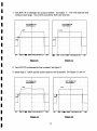
7. Tum R31 CW very gradually until a
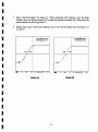
waveform similar to figure 1 is obtained
The tiimpot will have no effect the first
one or two tums, then it will begin to
have effect. Continue to tum the trimpot
CW until the oscillations just die out
before the next half cycle of the input
signal.
Figure 1.
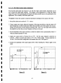
8. Tum R28 CW until the first overshoot is minimized, i.e. at the same amplitude as the settled
position. See Figure 2.
9. Tum R25 CW the first undershoot is minimized, i.e. at the same amplitude as the settied
position. See Figure 3.
34
. . . . , '•'TT-!
:
CH1=PositionOut
CH2=Position In
:CH1:
A /
CH1
1
•
A/
1
1
CH2
•
:
:
:
/
CH2
•
•
•
•
•
•
!
'
!
•
r'
+
t
t
•
:
/
/
J.
T
I
-
1 ii :
•
/
. . . ._i_.
t
•
. • . . !
CH<=Position Out
CH2=Position In
:
•
J.
,
;....;.
;
^
h^
1\ ~+
•
1A_
/
\ 4-
r
•
+
/
t
t
t
•
1
1
iii
- r r-TH
^....,..,
t
.
.
.
.
.
2AAmV ^ Ch2 2 A'AmV' ^« M "Sms
Ext J
:
•
.
.
.
i
•
1.48 V
HBI
:
4
:
:
J.
2(KlmV \ Ch2 20«mV !i.M
Figure 2.
Sms
Ext /
i.46V
Figure 3.
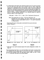
10. Tum R59 CW until the second overshoot is minimized, i.e. at the same amplitude as the
settied position. See Figure 4.
11. Tum R25 CW until the undershoot is minimized. See Figure 5.
CH1=Position Out
CH2=Position In
: cm:
X 1
CH2
CH1
V T ••
.
h....:...:.
rY-
/
i
:CH2
. / : . . . . ; , , „ :
CH1=Posltion Out
CH2=Positlon In
•
,.,,,.
V T " " : " "•;
/:
/,:,,..:,..,
.
:
:
i
T
i
•
:
i
•
:
1
;
r-'
4T
•
\;
'.
'.
:
1
+
t
i
.
.
.
4.
J.
•
.
.
•
.
.
•
.
i
•
:
:
:
:
.
,
'
HH
Figure 4.
;....;....
•
4-
t
IT
1
tT
'
T
... . . ^ . . . . . . . . . . . . . . . . . . . . . ,
J.
.
X
.
.
.
.
200mV ^ Ch2 2 AOmV'^M ' Sms' Ix t
Figure 5.
35
^
\i : : 1:
.
/
.
1.46 V
+ CHi=Position Out
I CH2=Posltion In
: CH1:
....
t\ •:
•CH2
•••••
12. Tum R28 until the first overshoot is
minimized. See Figure 6.
/
-
/
:
^
i
:
:
•
Jl
^1
i,
.
.
.
.
.
.
.
.
.
:...
[ , . . . . ! . . . .
i..T...:....:...
r,
1
Figure 6.
1 .
.
.
.
1
.
il : :
1
T
•
•
1
•
•
•
•
1
J.
1
1
.
.
.
.
.
.
.
.
.
.
.
.
EHiii 200inV Vl Ch2 20(lmV ViM Sms Ext / 346mV
13. To increase the speed ofthe system (decrease the step response time) still further, slowly
tum R31 CW a few more tums, then re-tweak the other trimpots as before to make the
waveform look critically damped again. This can be continued until the desired small-angle
step response time is obtained or the system begins to resonate or "ring". If this ringing
occurs, immediately tum back the trimpots starting with R31, then R28, then R25, and then
R59 until this stops. Tum each trimpot CCW gradually and evenly, similar to when the loop
gain was increased. Do not operate the system with the loop gain tumed up so high that the
servo rings anywhere in the field. Experience with the system will determine how fast it
should be tuned. Call Cambridge Technology Inc. for more information on this subject.
Refer to figure #7 for how the waveform should appear after iterating through the above
steps.
•
•
•
•
f
: CH1:
Note the critical damping infigure7. There is no
appreciable overshoot nor undershoot. The step
response for this scanner/servo system is about
2msec. The scanner is considered settied ^\iien
the position signal has settied to within about 1%
ofthe length ofthe step. The exact step response
time will vary from system to system depending
on load dynamics and scanner size.
/
•CH2
•
t
................^.........
:
:
.
t
.
• CH1=PositionOut
. PH^BPncifinn In
7
1
1
.
....:....:....:.. .1...:....
\
T
:
Figure 7.
:
i.
:
:
:
.
:
:
.
:
:
.
;
:
.
:
i
1
•
;
•
[JHA ' 20irmV \ ai2 200mV \ M 2.5ms Ext /
36
346mv
6.1.7.1.2. Fine Tuning
The purpose of this section is to adjust more carefully the "shoulder" ofthe step response.
1. Setup the system by performing steps 1,4, and 6 from section 6.1.7.1.1. above.
2. Tum on the system power.
3. Adjust the input signal amplitude and offset so that the scanner now steps from -2.0° to 0.0° in
a square wave fashion and at the same frequency as before.
4. Adjust the oscilloscope channel monitoring Vp to lOmV/div. The system should now look
like Figure 8.
Note: Since only the coarse tuning has been performed thus far, your waveform may look
slightiy different at this point. However, the same tuning mles still apply.
5. Tum R28 CCW to bring the first overshoot at the same level as the settled waveform. See
figure 9.
CH1=PositionOut
CH2=Posaion In
CH Imposition Out
CH2=Position In
CHI
CH1
CH2
CH2
Chi
I6mi^ k MB iiftnii/ ^. M I5ms i x U U /
1.58 V
Figure 8.
Chi ' lamO C MM SftftmV' ^ M iS'ms i M \ 6 /
Figure 9.
6. Tum R25 CW to eliminate the first undershoot. See Figure 10.
37
1.58 V
7. Tum R59 CW to eliminate the second overshoot. See Figure 11. This will make the first
overshoot much larger. This will be corrected by R28 in the next step.
:
['"•
:
.
+
T
T
r
:
Cn1=PosiDon Out
; CH2=Position In
(;H2=Position In :
[
4-
CHI-
[
T
i
^~-,
T
•
:
•
/ .
1
1•
-
Ol-ll mPnolinn rWrt:
•
j... p..l.;....i....i....^...:...,
•
CH1
:
j
•
•
•
•
..:....:
t
•
•
•
T
•
•
•
I
.
:
.
i
.
.
.
+
;
fcH2
•
;
;
. 1
fCH2
;
:
:
::
:
j
•
•
:
1
+
:
:
•
t
•
:
t
I
:
:
j
:
itimtf V i n
i i i m v '^M2.Sms Extyid/
I
:
+
.
.
.
I
:
•
:
:
^
.
.
I
:
:
j.
.
i
4-
-
Chi
?
.
.
.
IdmV K Ch2 SAAmV ^M 2.5ms Ext; 10/
issv
Figure 10.
i.SSV^
Figure 11.
8. Tum R28 CW to eliminate the first overshoot. Seefigure12.
9. Iterate steps 6, 7 and 8 until the system settles as well as possible. See Figures 13. and 14.
+
J
CH1=PositionOut
CH2=Position In
.
CHi:
CHI
r~
:
/
[CH2
CH2
:
r
'.
i.58 V
38
:
T
.
- '
•
•
:
•
:
.
.
•
1-
•
.
.
•
•
.
•
•
•
.
T
i
4-
ilIm^
'.
:
'
•
•
,
.
•
•
r
•
1
'.
j.
J.
•
1
.
.
•
•
•
'.
.
.
.
.
.
V l i i l itbmV ^iM2.SmsExtyiO/
Figure 13.
Figure 12.
•
'
.
:
:
;
tChi
St
i
"
f " : "1
' \irr/j K 'Mffi Sft'drnV '\> M 5.S'ms i x V U j
•
.
. . . . ' . . Cm^osilion Out .
: CH2=Position In
+
Chi
•
.
i.SS V
•
- - - - I - • • • ! • • • - ! • • • • ! • • •
•
: '
.
:
:
•
' •
'
CH1 :
Note: Whenever the small angle step response
is changed, the large angle step response
should be checked in the Slew Rate Limiter
Speed Adjustment section 6.1.7.1.3.
.
I -
• • • ! • • • •
i • • •
•
CHI =Posltion Out
CH2=Position In
i
:
:
_
1
1
T
:cH2
t
':
Figure 14.
d
I
;
m
39
»OmV K Ch2 SAOmV <;.M 2.5ms Ext;id- 7
1.58 V
6.1.7.1.3. Slew Rate Limiter Speed Adjustment
Now that the small angle step response is set, the Slew Rate Limiter Speed Adjustment can be
set to contiol the large angle response. The purpose of this adjustment is to keep the output
stage ofthe servo from saturating for the largest and fastest possible move to be performed in the
application. This is usually a full-field square wave.
**Caution!! Ensure the scanner is properly heatsinked or damage to the scanner will result.
1. Set up the system as in section 6.1.7.1.1. above.
2. Using a square wave input, adjust thefrequencyofthe input waveform so that the motor will
have enough time to settie at each point before the next half cycle ofthe square wave occurs.
If that is not yet known, run the system at around 30 Hz. Note: For very large inertia systems
this might be too fast, thus a slowerfrequencywill have to be used.
3. Set the amplitude ofthe input waveform so that the scanner moves symmetrically about 1.0
volts p-p centered around 0.0 volts.
4. Attach one scope probe to Position Out on TPl. Set the scope channel's sensitivity to
0.5V/div. Attach a second scope probe to Fl to the +Motor signal. Set the sensitivity to
1 OV/div. This is the drive voltage sent to the scanner drive coil. See Figure 15.
5. Increase the amplitude of the input signal slowly while watching the +Motor signal on the
scope.
: CHi:
;
CH1=PosilionOut
CH2=+Motor
,
1
:
:
T
•
:CH2
'
: CH2=+Motor
CHI
•....1
.
^^_.
,
; 1
;
i
.
T
:,:
1
: ^^^ ^I^
+
SdJmtl KI d n i
' 16V' CM J.Stns E x t / U /
1.58 V
wa
p/
:
•;
sournv >«« ai2
10V ^M
Figure 16.
Figure 15.
40
•
•
^ :: ^
" i " T "T"
. 1- (-
:
•
1ms Ext/10 J-
'
1.58 V
6. As needed, adjust the Slew Rate Limiter Adjustment trimpot, R78, CW to slow the maximum
slew rate of this large angle square wave as needed to keep the +Motor voltage from
"squaring off' or saturating at the top of the first peak. Figure 16 shows this squaring off
phenomenon. Slowing down the input signal will increase the large-angle step response time.
However, the best setding performance will by achieved when the output amplifier is not
allowed to saturate. To ensure the output amplifier will not saturate even after the scanner
reaches its maximum operating temperature, use the following formula for setting the
maximum voltage on +Motor during the step:
+Motorpeak = (+|Drive-2V)/1.3
where: +Drive = Input power to the servo card
Note: In the example above, the +Drive = +28V, thus +Motor peak = 20V.
Depending upon motor impedance, load inertia, system tuning, power supply
voltages, etc., the max output amplifier current of +/- lOA may be reached prior
to voltage saturation.
Keep tuming R78 until the +Motor peak is at the desired level as given by the above
formula. Seefigure17.
5V K Chi • 10V' CMlSmsExt/i6/ 1.58V
Figure 17.
FigurelS.
7. Iterate steps 5 and 6 until the maximum angle for the system configuration is reached. See
Figure 18.
If the Command Input Scale Factor is set so that the fieldsize ofthe system is less than the fiill
+/-20° mechanical, then the position output, Vp, will not tiavel the whole +/-I0volts. Since the
slew rate limiter sometimes affects the small angle response slightiy, go back to section
6.1.7.1.2. to check that it the system is still critically damped.
41
6.1.7.2 Class 0
The object of this procedure is to bring the servo gain up slowly while maintaining contiol ofthe
scanners at alltimes.Move all the trimpots in small increments until experience with this system
is obtained. If at any time during this procedure the scanners start to move erratically and make
a loud buzzing noise, shut off the input power immediately and check the procedure to see if all
steps were followed properly.
6.1.7.2.1. Coarse Tuning
1. Perform steps 1 - 7 in section 4.2. above.
2. hiitialize all tuning pots. Tum R25, R28, R31 and R59 counter-clockwise, CCW, at least 15
tums or until they begin to click. Do not touch R107. It has been factory set and should not
need adjusting at this time. Tum R78 fully CCW 15 tums. Ensure Wl and W6 are
connecting pins 1 and 2.
3. Tum R25, R28 and R59 2-3 fiill tiims CW. This should allow tiie scanner to center vkitii a
slight amount of loop gain once the power is applied. It also allows the input signal to pass
through the system, so be careful when tuming on power in step 5 below. Ensure the input
signal is set to a DC voltage of O.Ovolts.
4. Attach a scope probe to the input signal at W4 to monitor the input signal. Use the rising
edge of this signal as the trigger source for the scope. Attach another scope probe to TPl to
monitor the Position Output signal, VP. Use TP2 or W7.2 as the ground reference for both
signals. Set the vertical gain to 0.2V/div for both channels on the scope.
5. Apply power to the system. The system should perform its normal tum-on sequence and both
scanners should center themselves. Check the voltage at TPl to ensure that the scanner is
some^^iiat near the center ofthe field. (Within ~1 volt.) If the scanner has not yet centered,
turn R25 and R28 CW a littie more while carefiilly watching the oscilloscope for any erratic
behavior. Ensure that the servo loop is slightiy "stiff' by attempting to move the mirror.
Touch the mirror only by the edges to avoid fingerprints. The use of finger cots is highly
recommended. When the servo is stiff, the nurror will resist slight efforts to move it, and
center again when released. Once this is obtained, continue on to the next step.
**Caution!! If at this time a load buzzing or whining noise is heard from the scanners, shut off
the power immediately. Tum R28 CCW one full tum and try applying power again. If the
system is still not behaving well, start over at step 1, using less tums for step 3. If the system
cannot be made to work, call Cambridge Technology for assistance.
6. Input a square wave input signal at afrequencyof 30Hz. Set the amplitude to produce about
2° p-p of scanner shaft motion. The exact amount is not important as long as the motion is
small.
42
7. The scanner should now be responding to the input waveform, but should look very
underdamped. Continue to turn R28 CW until the oscillations just die out before the next half
cycle ofthe input signal. See figure 19.
8. Turn R25 CW to minimize the first overshoot and to minimize the oscillations. See figure 20.
HfD 20omV % (inz 200mV ^M 5msfext/io/ 1.58V
Figure 19.
'HB 2' fl6mV ^^ Chi mmV KfA 5msExt/ld/ 1.58V
Figure 20.
9. Tum R59 CW until the undershoot is minimized, i.e. at the same amplitude as the settled
position. See Figure 21.
10. Tum R25 CW until the first overshoot is minimized, i.e. at the same amplitude as the settled
position. See Figure 22.
43
CHI
/
•
CH1=Position Out
CH2=Posttion In
:
:
:
:
1
• ! •
4
. : . . . :
'•
CH2
T
T
i
,..:....!....
+
t
T
T
•
1
:
r^-....:....:.... :l
\i
:
J,
'
:
:
:
:
.
t
T
T
T
i.
J.
2'MmV V M " S m s E x t y i d /
i.S8V
^iii
i i i m i / K t h i itdmV KU ' Smstxtyid/
Figure 21.
1.58 V
Figure 22.
•• • • 1• .• .I• • • • !
11. Iterate steps 9 and 10 above until the
waveform is critically damped as shown in
figure 23.
CH1
CH1=PositionOut •
CH2=Position In
J.
/
••
:CM2' - . / . . : .
J.
(
/
•
:
.
.
.
:
•
4
Figure 23.
+
_ l
•
'....:....:....:
li ;
'
+
!
•
•
;
•
:
•
:
•
12. To increase the speed of the system
t
.
J.
i
(decrease the step response time) still
.
.
.
.
I
.
.
.
.
.
further, slowly tum R28 CW a few more
200mV
\i
ai2
200mV
VM
SmsExVIO/
1.58V
mn
tums, then re-tweak the other trimpots as
before to make the waveform look critically damped again. This can be done until the
desired small-angle step response time is obtained or the system begins to resonate or "ring".
If this ringing occurs, immediately tum back the trimpots starting v^th R28, then R25 and
then R59 until this stops. Turn each trimpot CCW gradually and evenly, similar to when the
loop gain was increased. Do not operate the system with the loop gain tumed up so high that
the servo rings anywhere in the field. Experience with the system will determine how fast it
should be tuned. Call Cambridge Technology Inc. for more information on this subject.
Refer tofigure24 for proper tuning after iterating through the above steps.
44
:
:
:
:
:
-^/
Note the critical damping in figure 24.
There is no appreciable overshoot nor
undershoot. The step response for this
scanner/servo system is about 1.25msec.
The scarmer is considered settled when the
position signal has settled to within about
1% ofthe length ofthe step. The exact step
response time will vary from system to
system depending on load dynamics and
scanner size.
(
:.
•
/ • • . - . •
1
•
•
•
t
t
: CHi=PosiiionOut
CH2=Position In
\
•
r..
-.. 1
•
t
•
•
t
•pH2
T
J.
;
:
;
+
t
.
T
T
^ ....
... \...}....:•... i..:•....:•.
T
:
Figure 24.
:
:
Chi 206mV
45
'
i
4-
l ::
:
T
:
.
:
.
:
.
-mm—MismsExtyij/
:
:
.
i.$iv
6.1.7.2.2. Fine Tuning
1. Setup the system by performing steps 1,4, and 6 from section 6.1.7.2.1. above.
2. Tum on the system power.
3. Adjust the input signal amplitude and offset so that the scanner now steps from -2.0° to 0.0° in
a square wave fashion and at the samefrequencyas before.
4. Adjust the oscilloscope channel monitoring Vp to lOmV/div. The system should now look
like Figure 25.
Note: Since only the coarse tuning has been performed thus far, your waveform may look
slightly different at this point. However, the same tuning rules still apply.
5. Tum R59 CW to minimize the amplitude ofthe undershoot as shown in Figure 26.
. . . . . . . .
i . . . . : . . . .
1 . . . . : . . . .
:
.
1 . . . .
•
•
.. ..
:
:
^T..T..;.•....i....:....;
K..,^.^
; CH1
^ • ! • • • • ! ' ' • • _ ; _ • • • •
T
T CH1=Pos)tion Out
{ CH2=Position In
;
' • • • ! • • • • ! • •
T
•
+ _•
:
I
:
•
.
•
•
_
:
:
;
:
:
!
CH1
:
i
I
4
• •
•
.
^ !
•
.
•
•
•
;
•
•
•
.
.
.
.
•
•
.
CH1=PositionOut
CH2=PosHion In
.
!
:
:
.
•
-^
.
.
-
•V
f
-
. • • • • J "
4
4.
M
•
•]
:••••:
•
•
i.
1
CH2
:
CH2
:
:
:
T
:
:
1
; ; :
+
: :
1
•
•
•
;
T
X
J.
1
1JmV
( h2 SOimV
M 2.5ms Ext/ifi/
'1.81V
^m' '
1.
lOmV
Ch2 SOOmV
M 2.5ms ExtyiO/
Figure 26
Figure 25
6. Tum R25 CW to eliminate the overshoot. See Figure 27.
7. Iterate steps 5 and 6 until the system settles as well as possible. Seefigures28 and 29.
46
1.91V
I
.
.
.
.
J
.
.
.
.
:
.
:
:
:
.
•
L .
. .
;
.
[
.
.
:
'
~.. •CH1=Position Out
i
CH2=Posilion in
i
.
.
.
:
:
:
• CHr
. t
1.. CH1=Position CXit •'•••• 1
; CH2=Position tn
:
: CHi:
r
[
fv^''":
[
' :
:•-•;-••:•
•
CH2
r
•
i
•
:
i
:
-
' i • • • 1 i • - !
•
r^-^""'"
•
:
L
"
|.
.
!
•
•
:
:
"T'" ' • • ' " • • •'
:
;
;
"•
•
•
hCH2
r
1
•
+
.
X
;
;
:
:
1
•
[
•
;
:
:
:
:
[
•
!
:
•'
•
: "
:
:
:
:
HBI 16mV ' Chi SflOmV
•
t
•
:
•
M 2.5ms Ext/10/
1.91V
m
:
;
I
Chi 566mV
1JmV
Figure 27.
:
:
M 2.5ms Ext/10/
1.91V
Figure 28.
'T-r . . ^ . . . .
X
I
Note: Whenever the small angle step
response is changed, the large angle step
response should be checked in the Slew Rate
Limiter Speed Adjustment section 6.1.7.1.3.
[
GH1
I ....
I . . . .1 . . . . ! . . .
.
CH1=PositionOut
CH2=Position In
•
+
t
^
: / ^
:
•
T
T
t
•'•
,
T
CH2
t
T
•
1
''
M
Figure 29.
=•: ^ I
•
•
•
Hii
47
200mV
Ch2 5 66mV
•
" M i ^ m s Ext/Id /
i.91 V
6.1.8. Aligning the Mirror
This procedure describes how to align the scanner mirror (load) while the servo is still active.
Since the servo normally interprets someone holding or touching the mirror as a change in the
inertia ofthe mirror, the system usually goes unstable. The Mirror Alignment Mode jumper, W5,
when activated, lowers the loop gain, allowing the user to loosen the mirrors while the servo is
still active, but without it going unstable.
Note: This procedure can only be used to align the mirror to the center of its range. It cannot be
used to align the mirrors to some other point in the field. The Mirror Alignment Mode jumper
forces the scanner to go to the centered position.
1. Setup the system by following steps 1 - 7 in section 4.2. above. The system must have had
the Position Output Scale Factor, the Command Input Scale Factor, and the Closed Loop
Response already adjusted properly either by CTI, or by the above procedures.
2. Send a digital 32768io to both chaimels for digital inputs, or send a 0.000 volt signal for
analog inputs. Ensure the Command Input Offset trimpot Rl is set to 0.000 volts by
monitoring on the wiper of R1.
3. Remove the jumper, W5, from connecting pins 2 and 3, and re-insert it onto pins 1 and 2.
The system is now set up in Mirror Alignment Mode.
4. Tum the power on. The system should tum on in the normal sequence, except the mirrors
will stay at the center position.
5. The mirtor mount clamp screws can now be loosened.
6. Referring to the proper XY Mount Interface Dwg in section 6.2. locate the entiance and exit
points for the mount.
7. Align a laser beam so that it enters the entrance pupil perpendicularly to that side of the
mount. Make sure it is perpendicular in both the vertical and horizontal axes.
8. Place a target some distance from the mount to capture the exiting beam. Position the target
so that a beam exiting the XY mount is at the exit pupil and perpendicular to the entering
beam.
9. Adjust the mirrors in the XY mount so that the exiting beam strikes the center ofthe target.
10. Make sure the mirrors are pushed all the way down the shaft. Tighten the screws securely,
but not sotightas to strip out the small Allen heads.
11. Re-install W5 back to its Normal Mode location, connecting pins 2 and 3. Ensure the
position ofthe beam is still centered.
48
Note: There may be a small offset in position from Mirror Alignment Mode to Normal Mode.
This is due to any friction and/or spring in the scanner and because ofthe reduced loop gain. To
account for this, offset the mirror the same amount but in the opposite direction of the original
offset. This can be done because this offset is most often very repeatable.
49
6.1.9. Matching Two Servo (X and Y) Channels
The purpose of this section is to match the dynamic performances of a dual axis X and Y system
over all angles and frequencies. This system would consist of two 670 boards and two scanners.
If the two channels are not closely matched, the system will not make sfraight lines when both
channels are moved simultaneously. They also will not retrace a pattem when the beam is
traveling in the opposite direction. Thus, it is cmcial for optimum performance to perform this
procedure whenever either servo channel has been retimed. This matching is done standard at
(Zlambridge Technology and should not need to be repeated during the normal operating life of
the system.
1. Set up the system by following steps 1 - 7 in section 4.2. The system must have had its
Command Input Scale Factor, Position Output Scale Factor, and Closed Loop Response
adjusted properly to perform this. Ensure the mirrors are aligned by following the procedure
in section 7.1.8., to eliminate the chance of their hitting.
2. Input a 30 Hz square wave signal such that the scanners move 2° mechanical peak-to-peak.
For larger systems a slower square wave can be used. It is very important that the two
channels receive the information simultaneously, or this procedure cannot be performed
properly. For analog input systems, this is easily done by using a BNC "T" connector and
hooking up to both inputs simultaneously. If the system is digital, do not let a timing skew
occur between the X and Y channels. Let both channels' CS lines go low simultaneously. If
this is not possible, convert the 670 for analog input operation for the purpose of this
procedure.
3. Tum on the system power. Monitor both channels' position out signals, Vp on TPl, on an
oscilloscope while extemally triggering the scope on the input signal at W4. Monitor the
channel with the greater inertia first. This is usually the slower system. In most cases this is
the Y-channel. Ensure the step response is at the required speed for the application and that
it looks critically damped. Refer to the timing procedure above in section 7.1.7. for specific
instmctions. If it is not tuned as required, retune this channel now.
4. Input a full-field signal. Monitor the same channel and ensure that the large signal step
response is also as desired. Once this is accepted, do not tum any ofthe pots associated with
this channel or this procedure must be started over again.
5. Input a 2° signal again. Now monitor both channels' Position Out signals superimposed on
one another on the oscilloscope. Increase the vertical gain and sweep speed on the
oscilloscope until the speed difference between the two channels is noticeable. See Figures
30 and 31.
50
;
t
4T
^
•
.
.
^
-
•
.
.
.
.
.
.
•
.
.
.
•
.
.
;
+
•
.
:
:
:
T
.
.:....^: i ^
?^'*'^'
:
:
:
:
• jj
•
:r
1
:
:
ff
-i-
:
:
•
T
t
7
GH1 1 CH2
CHi=Position out, x
CH2=Position out, Y
•
•
"
• CHi=Kosraon<Jui,A
; CH2=Position Out, Y
;
CH1 / / : CH2
J.
.
4-
.
1
•
+
.
.
.
.
•
:
.
.
•
•
.
•
:
:
:
J /
J,
.
T
•
.
.
•
•
[IK ibimV
•
.
.
.
^
•
'^^r\T\
•
.
/
" / /
•
M ImsExt/iO
^
•
,
.
-r
j.
Chi '266m ;
.
;
•
:
. . . . . . . . . . . .^. . . . . . . . . . . . . . . . . . . . . . . ..
•
:
•
;
7 / /
r//
:
"*•
,
:
L
1.91V
Chi 2eAmV
HH 206mV
Figure 30.
M250us E x t / i t /
1.91 V
Figure 31.
6. Slow the faster servo channel as necessary by adjusting its servo adjustment trimpots slightiy.
Refer to section 6.1.7. for proper operation of all the tuning trimpots. Ensure that the
channel is still critically damped when done. Do not adjust this channel's slew rate limiter
trimpot at this time. Be patient. The faster channel should be slowed to track the first
almost perfectiy. When done, the system should look like Figures 32 and 33.
• • - • ! • • - : • • • • ! • • • ; - • • •
CH1-'PoBilionOut X
: CH2=Position Out, Y
]^ • •
'
I
. . . . . . . . . . . . . . . . . . i^y^^V
: /
/
1
Chi 24«mV
'2fl6mV'' M ' 1ms E x t / l i l /
1.91 V
^
Chi iiimV
Figure 32.
- ! -- - - :
:
I
.
j
—•
^^^
• •
•
- •
•
•
•
:
?
:
:
1
.
j.
i
.
.
EiOS 266mV'
•••-
.
.
.
.
.
•
:
.
.
.
M2Mus Ext/16/
Figure 33.
51
• • - • 1 ' • • •: • • • •
:
,
.
.
,
.
i.91 V
7. Input a full-field signal. See figure 34. While monitoring both channels, slow the faster
channel's slew rate limiter trimpot, R78 to make the signals are equally fast. When done, the
system should look like Figure and 35.
8. Repeat steps 6 and 7 until both conditions can be met and the outputs look like figures 32,
33, and 35.
I
T
CH1=PositionOut,X
CH2=Position Out, Y
1
1
/ !
:
;
: Ch
/
•
•
CH1=PositionOut,X
CH2=Posilion Out, Y
[ ' . ' . ' . ' .
1
' . ' . ' .
L
.
X
.
L
.
y ^ J,
.
.
.
.
.
.
.
.
'.
.
.
.
.
.
.
.
I
i
:H2
//. •
/
^ -^
1
;
:
j.
; CH1 / CH^
•
/
t
•
t
•
1 • y
t
•
T
4-
•
1
m'
iv ' tTiJ-^
SV'
M 1ms Ext/10 /
f t-^
•
• ...i..."
•
•
•
•
\.
L
.
.
;
i.91V
Hil '
•
.
.
5V
.
.
.
.
Chi
T
•
•
•
•
T
•
•
•
•
L
J.
.
.
SV
.
.
.
.
M ImsExt/lO
i.91 V
Figure 35.
Figure 34.
52
.
.
.
.
6.2. 6740-XX Notch FUter Module
6.2.1 Background Theorv
All mechanical systems are subject to vibrations via extemal excitation forces. The degrees of
freedom of a vibrating mechanical system are defined by the number of independent coordinates
required to identify its displacement during vibration. If we have a Cartesian coordinate system
witii X, y, and z axis, then for a freely vibrating body, we can have six degrees offreedom.This
includes translational and rotational vibration in each of the three axis. Each of these possible
vibrations is referred to as a mode of vibration. Each mode of vibration has a natural frequency
associated with it that is independent of all the other modes.
For our discussion with respect to the scanner, we will concenfrate on the rotational axial mode
of vibration. The natural frequency Fr of this mode is a fimction of the mirror load inertia and
rotor inertia as well as the torsional spring constant of the rotor shaft which couples the two
inertias. The undamped natural resonant frequency of this mechanical system is described by the
equation below:
COR = k ' ^ [ ( J , + J 2 ) / J , J 2 ] ' ' ' , Fr=(OR/27t
where k = rotor torsional spring constant
Jl = mirror load inertia
J2 = rotor inertia
Note that in a real mechanical scanner system damping due to bearing friction, air friction on the
rotor and mirror load, etc. do indeed exist. However, CTI scanners exhibit very low bearing
friction, and the above equation will approximate the resonant frequency quite closely. The
damping constant inversely influences the natural resonantfrequencyslightly. In other words, as
the damping constant increases, the natural resonantfrequencydecreases.
This torsional resonant frequency can exhibit a high Q, which is defined in one sense as the
sharpness and amplitude of the resonant frequency peak. If this resonance occurs in a closed
loop servo system where the gain vsfrequencyhas fallen off enough that the (negative) position
feedback phase shift approaches 180°, and the amplitude peaking at resonance is enough that the
position feedback gain rises near unity, servo loop instability and oscillations will result. This is
the reason for using a notch filter in the forward path of the servo loop, after the summing
amplifier. The notch filter is tuned to remove thefrequencycomponent ofthe ertor drive signal
sent to the scanner confrol coil which is at the same frequency as the scanner torsional
resonance. This keeps the scanner from being excited at its resonantfrequency.The rejection of
this drivingfrequencyaids the stability ofthe servo by not exciting this natural resonant mode,
and allows the closed loop bandwidth ofthe system to be higher. Higher closed loop bandwidth
allows decreased step response times.
However, this does not mean that the scanner torsional resonance dissappears. Ideally, it is only
that the servo amplifier no longer "kicks" the scanner at this frequency.
53
6.2.2 Notch Filter Tuning Procedure
The 6740-XX Notch Filter Module (NFM) is designed to be inserted into J5 of the 670 servo
amp. The selection ofthe proper NFM is described below, along with tuning information.
Overview
This procedure indicates how to:
1) Determine the 1** torsional resonantfrequency(Fr) of a scanner and mirror load
combination
2) Select the proper 6740-xx Notch Filter Module (NFM)
3) Insert and Tune the NFM to the Fr
This procedure assumes the following:
-
A properly heat-sinked, working 670 board is hooked up to a power supply with
adequate current capability
A working scanner with mirror load is in an X-Y mount or test clamp similar to what
the end use would provide, and connected to the 670 board
The proper test equipment for normal system tuning is also set up and ready
The 670 schematic and outline drawings are in front of you.
The 6740 Notch Filter Module schematic is in front of you
Equipment Needed:
-
Oscilloscope (dual trace, minimum 60Mhz BW)
-
Frequency counter
* 670 board GND connection points: TP2, W7.2
6.2.2.1 Determining Fr;
a) Set signal generator to Ikhz sine wave, lowest amplitude. Note that we are assuming
that Fr will be above IKhz. Connect afrequencycounter to the output ofthe signal
generator with a "T" connector.
b) Without the NFM inserted into J5 (servo loop is broken), connect the signal generator
to TP6. Ground can be obtained on TP2 or W7.2.
c) Observe position (TP 1) and current (TP3) with scope.
d) Tum on power and signal generator.
54
e) Adjust the signal generator for about 200mV peak on current. This is a ballpark
> figure. The main concern is that the current through the coil be large enough to view
with good S/N ratio, but small enough to avoid excessive coil heating and mechanical
vibration ofthe scanner while performing this test. Maintain the position signal near
0 volts by adjusting the DC offset control ofthe function generator accordingly.
f) Slowly sweepfrequencyup while observing position and current on scope. Note the
frequency where a peaking occurs in the position and/or current waveform. This is Fr.
You can also hear the scanner become louder at Fr as well. When Fr is identified,
keep the signal generator at thisfrequencyand shut it off promptly, as well as board
power. Bearing wear will result if the scanner is held at the resonant frequency for
too long.
6.2.2.2. Selecting the proper 6740-xx NFM
The 6740-xx NFM's come in six different frequency ranges:
6740-06
6740-05
6740-04
6740-03
6740-02
6740-01
12.5-20 Khz
7-14 Khz
5-10 Khz
3.7-7.5 Khz
2.2-4.5 Khz
1.6-3.4 Khz
Select the proper NFM for the Fr measured in step (If) above. Choose one which the measured
Fr is closest to the center ofthe range.
6.2.23. Inserting and tuning the 6740-xx NFM
Make suretiiatthe 670 board is completely de-tuned. This section ofthe procedure will not work
otherwise.
a)
Insert the NFM with its solder side facing the 670 heatsink bracket.
b)
Connect TP4 to ground via jumper clip. This open circuits the output amp so that it will
not be driving the scanner during NFM adjustment
c)
Connect the signal generator to TP5. This is the summing amp input. Connect the scope
probe to TP6. This is the NFM output.
d)
Tum on the signal generator and observe the NFM output on the scope. The signal
generator should still be set at the resonantfrequencyFrfromthe previous measurement.
This is very important, since the NFM has a sharp attenuation characteristic. If the
frequency that the NFM is being tuned to reject is not exactly at the Fr ofthe scanner and
55
load combination,ringingmay still occur when tuning the scanner. This is especially true
for high Q scanner torsional resonances. The viscous damping coefficient increases as the
scanner RMS current (acceleration) increases, shifting the resonant frequency downward
slightly with higher tuning speeds. This tends to de-stabilize the system when a fixed
frequency, high Q notch filter is used. Lower Q notch filters can counteract this.
e)
Adjust the Frequency pot on the NFM until a minimum is obtained in the NFM output
waveform.
f)
Now adjust the Depth pot on the NFM to further minimize the output waveform.
g)
Repeat steps (e) and (f) until the NFM output waveform at Fr is minimized as much as
possible. At this point, you are done.
56
6 3 . Schematics and Assembly Drawings
This section contains the following schematic and assembly drawings.
670 Schematic
670 Assembly Drawing, Top Side
J, 670 Assembly Drawing, Bottom Side
4 670 Outiine Drawing
5 6010-1 Drive Cable Assembly Drawing
6 6010-8 Drive Cable Assembly Drawing
7 6010-8L Drive Cable Assembly Drawing
8 6010-11 Drive Cable Assembly Drawmg
9 6010-16 Drive Cable Assembly Drawing
10 ) 6010-17 Drive Cable Assembly Drawing
) 6010-17L Drive Cable Assembly Drawing
D03310
DOS311
D03312
D03457
D00898
DO 1978
DOB 187
D02430
D03188
D03190
D03189
57
TIT
U13
W2
nnisi
H 05 I h
IC4 I
rR40n
+ iL2Lh LmJ
-"
R52
""^
f[RW
T O ]l
nam
_
n
^i
^^
m
^1
I irn-g
mn
U15
REVB =
+
C13
^
*
I
*8
R24
]
W9,
UH2J
R6S
R66
C 3 ^
LQIJ
TP7 670 " 5 ^ V *
U9
w
U6
i«o
,LQ4J
J6
i nrwi
r
R42
^S n
J3
—'^
R30
iM
I
]»
U16
32B
[BD Ul nam e
J88
R81
TP^
rRTnren
S
in
rx^^xn
eT-^
nn
x j
LAYER 1 SILKSCREEN D03320 REV B
nu
x m - ±.009
( ) NOICATCS mm
AMOLCat o'-ao" , , .
MVMZ MMHtCS
V
•tCAKMLMMC tDCB
SSfSiwT
UStP OH
nNisr
•A
X3
UNLESS OTHERWSC SPCaRED
TOERWCeS
J(X - f.OtO
AS VIEWED FROM TOPSIDE OF BOARD
tzi
i RSS \ \
r'rtn
DRN
SES_
SSL.
ENC
-ea-
REVISON
B
CAMBRIDGC lEOtlOLiOOY. WC
109 SMITH PLACE
CAMBRIDOE. MA. 02138 - USA
670 SMD SERVO AMP.
ASSEMBLY DRAWING
TOPSIDE
D03311
IsHErr
or
HRSn
P9
(MU
fR^n
5io"'
rRsnrRsn g
OSS
UST f R s n
iRion
fRion
U4 [SS GSED U11
R47
R93
ESQ
Q48 1
I.
C7
EE
R45 1
r2
lmo3~l
PRsn R g ^ C S O i O 'Q3"' ^JL
U7
Ct6
R18
1-
OS
_m" U2
™,
U17
,[10 T3
iFNHr^=; CMU. .
XJUTmi] cEnQia
C12|
C9
LAYER 4 SILKSCREEN D03321 REV B
PARTS SEEN THROUGH TOP LAYER
(X-RAY VIEW)
UMI9S ODfinKE SPCOnED
lanANccs
.XX - i . 0 1 0
.MOT > ^ 0 0 5
( ) MNCATIS mn
AN(ua± v - x r
.
a m a MwtMS
v
MN
BB_
CHK
APPW
PMXCcnoN
UAffNAL
-EH3-
nasi—
B
CAMBMOGE TECtfMUMX M &
I M SMIH PUCC
CAMPWOGE. MA. 02138 - USA
670 SMD SERVO AMP.
ASSEMBLY DRAWING
BOnOM SIDE
003312
J l ( * PINl COMMAND INPUT CONNECTOR
Z632.50-
•m*
Tcm.
2_S5-
F4 0
TP3 0
©
TPl
:o)
r^l1J6 I
oaTAL mpuT ocnoN
D
II
670
In G o o j o
REV B
J3
Wll
PIN 1
1
2
3
d
51l
tr
IA
- MOTOR
PD S H i a o
AGC CUT
IB
J3 (4 PIN) INPUT POWER CONNECTOR
FIN i
ik
i
®
IfflE
#
5
^
I T 333
3
+ DRrt VOLTAGE INPUT
i
3
+ Wivt «10ftN (4W11
- CRIVE RETURN ICNoi
- CPIVE VaTAGE INPUT
C
5
t)
3
PINl
1
2
3
4
5
TRIM
Rl
RI3
9CNAL NAME
NOTCH FITER INPUT
NOTCH HLTER OUTPUT
+ ISV
CNbJtl
- iSv
1
2
3
4
5
LABa
3
ilR
fieis
1
DBI4
05^
DBI2
SIGNAL NAME
CS
m
DB10
GND
UK
R/W
Dfes
GND
0^9
085
DBO
GND
DB7
GND
DB2
GND
'5
16
LS Bit
oei
GNa._
DB3
GNO
DB4
GND
GTJD
iS
+ l5V
- ibv
MS B i t
DAC latch
tei 3
1 19'
20
21
1 22
23
24
._25...
26
27
VDAC16
GND p
+ VRtF
- VREF
GND h
+ 5V
NOTES
bSs
'7
18
J6 (8 PIN) DIOTAL INPUT OPTION HEADER
RN 1
1 PIN 1
1
2
4
5
6
7
8
9
10
1 11
1^13
14
GND f 4
9QX MAX PWR F U G O U K V
TAuLf fbW fluh^fr
REMOTE SHUTDOWN INPUT
J5 ( 5 PINl NOTCH FILTER HEADER
B
P107
SIZE
7
-.36
R7a
M 2 5 THRU
«.145 THRU
«.12b THRU, #.250 C'SINK FARSIDE
M
li
ERROR OUT
e
1
R51
R59
R77
OTY
6
i
-.81
ftM
R3I
HOLE
A
SIGNAL NAME
1
4
s #
VELOaTY OUT
POSITION OUT
8
SIGMAl NAME
+ MOTCR
MOTOP SHIELD
AGC FET
DIODE COMMON
9GNAL NAME
1
2
PINf
4
5
6
7
B
9
.rrai
PIN 1
J2 (9 RN 'D') MOTOR CONNECTOR
2
3
W5
COMM/^D GND (SHIELD)
COMMAND { + )
OFFSET INPUT
J l - ( 3 0 PIN) DtCITAI PARAI1.EL INTERFACE
J4 ( 8 PIN) OBSERVATION/CONTROL PCT!T
4
5
6
1
OTP2
9GNAL NAME
CdMI^ANb (-)
29
30
FUNCTION
POS. OFFSET (PO)
POS. 0£T. SCAl£ FACTOR (PS)
LOW rPEfl. DAUPINfi (LfB)
SffiVti OiN (Si)
EHWK NTECRATOft (!AiN (El)
ifiPUT 5cALE AbJusT (is)
HI fR'O tiUiP\U6 (HFTi)
POS UlT UNEARITY ADJUST (UN)
SLEW FAIE UMIIER (SRL)
HF DAilPING BANDWtOIH ADJ (BW)
TEST POINTS
TPl
1P2
tP3
^•4
1^5
TP6
1P7
FUNCTION
POSinON SGNAL, VP
GND #1
O i k k m hlONlTOt;
MUTE PIN
SUMMINii AMI* iNl^Ul'
NOTCH FILTER OUTPUT
AGC OUT
i M O S o n c M s c speorvD
TOEKAMXS
.XX « i a o i o
UA. I B t J I - USA
< } M X M T C mm
AHOLEU < r - » r „ .
unamjMos
OHM A i O v t f E C a S
v
-E3- ©
DEVtSCX
A
670 SMD SERVO
AMP. OUTLINE
D03457
2»
IscrT"
1h«9e drowixgs and specifications or* the property of
CAMBRIDGE TECHNaOGY and shoD no) be reproduced, or
copied, or used as the basis for the manufoclure. or
scde of opparotus without the written permission of
CAMBRIDGE TECHNaOGY. INC.
MALE AMLAN COS 9L (PO07O-OO90)
W/C880002I8) HOOD (P0070-0185)
lo
lb
A(x our
PO GND
SHIELD
+M010R
-MOTOR
SHIELD
8724 CABLE PO+OO-OOOI
t
RED
BLK
«
WHT
GRN
5
RED
BLK
?
8451 CABLE PO40O-0O36
REVISION
DESCRIPTION
DATE
ASSY VIEW ADDED
B/94
NOTES i t C a END PRtP WEW ADDED
LENGTH REDEFINED
MTl HOOO MFC | CHC'D. STNOOTF REMVD
FEMALE AMLAN CDF 9L (P0070-0082)
W/CB80002I81 HOOO (P0070-0185)
3 / 4 " TYP(4) —
•o 9
•o 4
-08
•oi
-o 7
-o 1
-o6
-o2
—
1/8" TINNED
TYP(t2)
J2
NOTE 5
FINISHED LENGTH
TOL = i l INCH OR ±5%
WHICHEVER IS GREATER
NOTES:
V 4 COND CABLE IS BELDEN TYPE 8724(PO40O-(X)O1)
2. 2 COND CABLE IS BELOEN TYPE 8451(P0400-0036)
3. 1/16 HEATSHRINK TUBING (PO43O-0O18)TO BE USED
ON SHIELD DRAIN WIRES.
4. +MOTCR IS DEnNED AS CAUSING A CW ROTATION OF THE OUPUT SHAFT
VIWEN +M0TOR IS DRIVEN POSITIVE MTH RESPECT TO -MOTOR
UNLESS OTHERWISE SPECIFIED
TOLERANCES
.XXi.OlO
.XXX±.0O5
( ) INDICATES m m
ANGLES± 0 * - 3 0 '
5. "FINISHED LENGTH" DEFINED BY -XXX.
EXAMPLE : D00898-012
FINISHED LENGTH = 12"
DRN
10/5/88
DES
CHK
ENG
MATERIAL
APPR
PROJECTION
FINISH
REVISION
B.A.
CAMBRIDGE TECHNOLOGY, INC.
2 i ELM ST.
WATERTOWN, MA. 02172 - USA
6010-1-XXX
SCANNER DRIVE CABLE
-E3-
6. MEDIAN CUT LENGTH (ON BOM) = FINISHED LENGTH.
USED ON
D
D00898
SCALE
: NONE
I SHEET
I
OF
I
Ihese drawings and spedlicotlons ore the property of
REVISION
CAMBRIDGE TECHNOLOGY and shell not be reproduced,
copied, or used os Ihe basis for the monufocture. or
sole of opparotus without the written permission of
(6)PLC'S WIRES ONLY
NOT ON SHIELDS
CAMBRIDGE TECHNaOGY, INC.
ECO
516
REV
10
rr-n
•
•
DATE
PTH
PIH
PIH
2/93
5/93
8/94
9/94
PaARIZATION NOTE FOR P2 REMOVED
642
STRIP It TIN NOTE ADDED
657
ITEM eUBBlES CORRECTED P 0 4 3 0 - t 3 WAS
PO430-0OI4
- I J UJ - 1 4 ABOVE RETURNED TO ORIG
5
PIH
PTH
PIH
PTH
DWG| 4 n i l E UPDATED, LENGTH UPDATED
oaao
aaaa
NOTE 7
A M U N CDS 9L (POO70-0090)
WITH C88000218 HOOD (P0070-0185)
FINISHED LENGTH
TOL = ± 1 INCH OR
i 5 % WHICHEVER IS GREATER
FACE VIEW OF PLUG
PI
9 ODIODE COMMON
AGC OUT
8 O-
AGC RET
3 O
SHIELD | 1
+MOTOR
-MOTOR
NOIES:
Cfl IPO4OO-0065 ( N E E W C ( N t l - 4 0 r - 4 0 2 )
4 O-
SHIELD #2
2. 2 CONDUCTOR VIIRE - C l l |PO4O0-0066 (NttWHP»11-40T-403)
oO
O
O
1079
FMSHED LENGTH NOIES aARIFlED
tt
A
BLK
7/96
8/97
-09
-O 1
WHT
U-
11/94
P2
REO
5 O-
1. 4 CONDUCTOR WIRE -
APPR
P2 CONNECTOR CHANGED
667
1
DESCRIPTION
-V
GRN
-O10
•03
02
-08
A
RED
0 5
BLK
-06
7
04
3. STRIP CABLE INSULATION BACK 3 / 4 " , STOP ft UN WIRE
WSULAflON BACK 1/6" 801H ENDS.
10 PIN AMP IJI102387-1 (P0070-0173)
4. USE HEATSHRINK TUBING | P O 4 3 0 - 0 0 t 4 OVERAU EWRY 1 2 '
CAPTURE FIRST PIECE UNDER HOOO ( P 0 0 7 0 - 0 0 9 I )
5. USE COPPER FOU - CH <P0700-Oa47 ON BOTH ENDS OF
EACH CABLE. FOO. MUST CONDUCT TO ITS CABLE'S DRAIN
WRE, AND MUST BE ISOLATED FROM EACH OTHER WITH
HEATSHRINK |P0430-OOI5
UNLESS OTHERVUSe SPECIFIED
TOLERANCES
4-0.-1 INCH
DRN
PTH
10/92 CAMBRIDGE TECHNOLOGY, INC.
OES
UDT
10/92
6. 4U0TDR IS DEFINED AS CAUSING A CW ROTATION OF TNE
OUTPUT SHAFT 1MLH +MOT0R IS DRIVEN POSITIVE WIIH
RESPECT 10 -MOTOR
( ) INDICATES m m
ANaESi 0-30'
MATERIAL
ENG
7. MEDIAN CUT LENGTH (ON BOM) - RNISHEO LENGTH.
8. "FINISHED LENGTH* DEFINED BY -XXX.
EXAMPLE 6 0 1 0 - 8 - 0 1 2
FINISHED LENGTH '
N/A
FINISH
12"
USED ON
1 0 9 SMITH P L A C E
CAI^BRIDGE. M A . 0 2 1 3 8
APPR
USA
PROJECTION
6010-8
68XX DRIVE CABLE
-E3-
D01978
REVISION
N/A
-
CHK
SCALE HONE
SHEET 1
OF
I
Theis drowlnfs and speciflcations ore the properly of
REVISION
CAMBRIOGE TECHNOLOGY ond shot not be reproduced, or
copied, cr used as the basis for Ihe monufocture, cr
(6)PLC'S WIRES ONLY
NOT ON SHIELDS
sole o l opparotus without the written permission of
CAMBRIOGE TECHNOLOGY. INC.
ECO
REV
97gA
APPR DATE
DESCRIPTION
pm 3/p7
N O I E S ADDED
M a HOOO MFG f CHC'D
1069
PIH
TW
AMLAN COS 9L (P0070-0090)
MTH C880002181 HOOD (P007O-0185)
NOTE 7
PI
RNISHED LENGTH
TOL =• ± 1 INCH OR
±5% WHICHEVER IS GREATER
la
lb
DIOOE COMMON
8 O3 O
SHELO | l
7 O-
1. 4 CONDUCTOR m z
- CH IPO400-0065 (NEEWCr<ll-«OT-402)
2. 2 CONDUCTOR NR( - CI) |P0400-0066 (NEEW(;|N1l-40(-4O3)
3. STRIP CA81E INSULATION BACK 3 / 4 " . STRIP * UN WRE
INSUUIKIN BACK 1 / 8 ' B01H ENDS.
-MOTOR
6 a2 O-
\J-
GRN
A
RED
DIODE COMMON
V
AGC OUT
SHiaO * l
1 O
SHIELD #2
la
lb
WHT
4 O-
AGC RET
A
BLK
9 O
AGC OUT
+MOTOR
NOTES:
RED
/V
5 O-
+M0T0R
BLK
y
-MOTOR
4. USE HEATSHRINK TUBING |P043»-0OI4 OVERAU EVERY 12'
CAPTURE FRST PIECE UNDER HOOO (PO07O-O09I)
5. USE COPPER F O l - CTI |P0700-0047 OH 9 PIN 'D' END OF
EACH CABLE. FCa MUST COWUCT TO ITS CABU'S DRAIN
MRE. AND MUST BE ISaATED FROM EACH OTHER MTH
HEATSHRflK r>0430-OOIS
6. 4UOT0R IS 0CF1NE0 AS CAUSING A CW ROTATION OF THE
OUIPUT SHAFT WHEN +MOTOR IS DRtVtN POSITIW WTH
RESPECT TO -MOTOR
7. "rWISHEO lEHCIH" OtnNEO BY -XXX.
EXAIPIE : 6 0 I D - 8 L - 0 I 2
FMSHED LENGTH -
12'
B. MEDIAN CUT LENGTH (ON BOM) = ITMSHEO lENGIH.
UNLESS OTHERWISE SPECIFIED
TOLERANCES
4-0,-1 INCH
DRN 03/04/97
( ) INDICATES mm
ANaES± 0'-30'
MATERIAL
ENC
N/A
9. 1 / I 6 ' HtAISWK 1U8NC (P0430-OOI8) TO BE
USED ON S«ELO DRAM NRES OH NQH-PI END.
OES
PTH
CAMBRIOGe TECHNOLOGY. INC.
2 3 ELM ST.
WATERTOWN. MA. 0 2 1 7 2 - USA
CHK
APPR
PROJECTION
6010-8L-XXX
68XX DRIVE CABLE
-EZ3-
D03187
REVISION
USED ON
H/A
SCALE NONE
ISHEET I
OF
I
CABLE INSUL STRIPPED BACK 3 / 4 "
TYP (4)PLC'S SEE CENTER AUX VIEW
INDIV WIRE INSUL STRIPPED & TINNED 1/8"
TYP (12)PLC'S SEE CENTER AUX VIEW
These drawings ond specifications are the property of
CAMBRIDGE TECHNOLOGY and shall not be reproduced, or
copied. Of used as the bosis for (he manufacture, or
sole of opporotus without the written permission of
CAMBRIOGE TECHNaOGY, INC.
REVISION
NOTE 8
FINISHED LENGTH
TOL = ±1 INCH OR ±5%
WHICHEVER IS GREATER
Jl
12'
TYP(2)
NOTE 6
3/4" TYP(4)
1/8" TINNED
TYP(12)
8724 CABLE P0400-0001
HTSHRNK P0430-0018
Jl END OF
8724 CABLE
(NOTE 4)
AMLAN CDF 9L (P0070-0082) FEMALE
W/C880002181 HOOD (P0070-0185)
NOTE 3
TYP(4)
NOTES:
1. 4 COND CABLE IS BELDEN TYPE 8724{P0400-0001)
^APPROX
+MOTOR
-MOTOR
SHIELD
5/8"
2. 2 COND CABLE IS BEIBEN TYPE 8760(P0400-006B)
3. 1/16 HEATSHRINK TUBING (P0430-00t8)TO BE USED
OH SHIELD DRAIN WIRES OF 8724 & 8760 CABLES.
4. 3/16 HEATSHRINK TUBING (P0430-0023) TO BE USED
ON 8724 CABLE AT Jl END TO COVER EXPOSED FOL END AS SHOWN.
:J - m
1 o6 o2. o-
AMP 206060-1 (P0070-0139) FEMALE
W/206358-1 CLAMP (P0070-0143)
FEM. CONTACT (P0070-0142)
AMLAN CDS 9L (P0070-0090)
W/C880002181 HOOD (P0070-0185)
MALE
5. 3 / 8 x 1 / 2 BLK HEATSHRINK TUBING (P0430-00I7) TO BE
BE USED OVERALL EVERY 12 INCHES.
UNLESS OTHERWISE SPECIFIED
TOLERANCES
( ) INDICATES
ANGLES*
mm
O'-JO'
ENG
APPR
MATERIAL
PROJECTION
FINISH
REVISION
8. "FINISHED LENGTH" DERNED BY -XXX.
EXAMPLE : 6010-11-012
FINISHED LENGTH = 12"
PTH
CAMBRIDGE TECHNOLOGY. INC.
2 3 ELM ST.
WATERTOWN. MA. 0 2 1 7 2 - USA
CHK
.XXX±.005
7. -FMOTOR IS DEFINED AS CAUSING A CW ROTATION OF THE OUTPUT SHAH
WHEN -l-MOTOR IS DRIVEN POSITIVE WITH RESPECT TO -MOTOR
DRN 6/2/94
DES
.XX±.010
6. 3/8x2.5 HEATSHRINK TUBING (P0430-0011) TO BE
PLACED 12 INCHES FROM EACH END OF THE CABLES AS SHOWN.
8760 CABLE P0400-0068
6509/6900 DRIVE CABLE
(6010-11-XXX)
-E3-
9. MEDIAN CUT LENGTH (ON BOM) = FINISHED LENGTH.
USED ON
D
D02430
SCALE
[SHEET 1
OF
1
These drawings and specifications are the property of
CAMBRIDGE TECHNOLOGY and shall not be reproduced, or
copied, or used os the basis for the monufocture, or
sale of opparotus without the written permission ot
CAMBRIDGE TECHNOLOGY. INC.
MALE AMLAN CDS 9L (P0070-0090)
W/C880002t8t HOOD (P0070-0185)
lo
lb
AGC OUT
PO GND
SHIELD
•l-MOTOR
-MOTOR
SHIELD
ECO REV
APPR DATE
MTL HOOO MFG § CHC'D. STNDOfFS REMV'D
PTH
7/97
RED
BLK
3/4" TYP(4)-*|
^
WHT
GRN
:5
DESCRIPTION
1069
FEMALE AMLAN CDF 9L (PO07O-0082)
W/C880002181 HOOD (P0070-0185)
8724 CABLE P0400-0001
e
REVISION
I*-
1/8" TINNED TfP(12)
RED
BLK
?
8760 CABLE P04O0-O068
J2
NOTE 5
FINISHED LENGTH
TOL = ±1 INCH OR ±5%
WHICHEVER IS GREATER
NOTES:
1. 4 COND CABLE IS BELDEN TYPE 8724<P0400-O0O1)
2. 2 COND CABLE IS BELDEN TYPE 876G(P0400-0068)
3. 1/16 HEATSHRINK TUBING (P0430-0018)T0 BE USED
ON SHIELD DRAIN WIRES.
4. -l-MOTOR IS DEFINED AS CAUSING A CW ROTATION OF THE OUTPUT SHAFT
WHEN +MOTOR IS DRIVEN POSITIVE WITH RESPECT TO -MOTOR
5. "RNISHED LENGTH" DEFINED BY -XXX.
EXAMPLE : 6 0 1 0 - 1 6 - 0 1 2
FINISHED LENGTH = 12"
6. MEDIAN CUT LENGTH (ON BOM) = FINISHED LENGTH.
USED ON
UNLESS OTHERWISE SPECIFIED
TOLERANCES
.XX±.010
.XXX±.D05
( ) INDICATES m m
ANGLESt 0 - 3 0 '
DRN
10/5/88
MATERIAL
PROJECTION
FINISH
REVISION
DES
B.A.
CAMBRIDGE TECHNOLOGY. INC.
2 3 ELM ST.
WATERTOWN. MA. 0 2 1 7 2 - USA
CHK
ENG
APPR
B
6010-16-XXX
SCANNER DRIVE CABLE
D03188
SCALE
: NONE
[sHEET
1
OF
I
These drawings ond specifications ore Ihe property of
CAMBRIDGE TECHNOLOGY and shall not be reproduced, or
copied, or used as Ihe bosIs for the manufacture, or
ECO
sole of apparatus wiihout (he written permission of
1069
CAMBRIDGE TECHNOLOGY. INC.
II8B
(6)PLC'S WIRES ONLY
NOT ON SHIELDS
NOTE 7
10
n-r
5
la
5 O-
lb
9
NOIES:
I 4 CONDUCTOR WRE - CTI |P0400-0065 (NEEWC|NIl-40T-402)
7/97
PTH
2/98
AGC RET
3 O
7
•O 1
WHT
M
GRN
O
-l-MOTOR
1 o-
-MOTOR
6 O
SHIELD #2
2 O-
2. 2 CONDUCTOR fURE - CH |P0400-0068 (BELDEN 8760)
-09
BLK
4 O8 O-
P2
RED
O
AGC OUT
SHIELD | 1
FACE VIEW OF PLUG
NOIE 4 P0430-00I7 WAS PO430-O0M
PI
DIODE COMMON
aa a a a
• •• • a
DATE
PTH
AMLAN CDS 9L ( P 0 0 7 0 - 0 0 9 0 )
WITH C880002181 HOOD (PO070-O185)
FINISHED LENGTH
TOL = ± 1 INCH OR
± 5 % WHICHEVER IS GREATER
1
REVISION
DESCRIPTION
MTL HOOO MFG | CHC'D
REV
CLR
BLK
-Oto
-03
02
-08
-05
-Oe
0 4
3. STRIP CABLE INSULATION BACK 3/4". SIRIP ft TIN MRE
WSUIATION BACK 1/8' BOTH ENDS.
to PIN AMP )jl102387-1 (P0070-0173)
4. USE HEATSHRINK TUBING |P0430-0017 OVERAa EVERY 12"
CAPIURE FIRST PIECE UNDER HOOO {P0070-0091)
5. USE COPPER FOIL - CH |PO7O0-0047 ON BOTH ENDS OF
EACH CABLE. FOL MUST CONDUCT TO ITS CABLE'S DRAIN
WRE, AND MUST BE ISOLATED FROM EACH OTHER MTH
HEATSHRINK |PO43O-0Ot5
UNLESS OTHERWISE SPECinED
TOLERANCES
-1-0,-1 INCH
DRN
6. >M0TOR IS DEFINED AS CAUSING A CW ROTATION OF THE
OUIPUT SHAFT WHEN +MOTOR IS DRIVEN POSITIVE WIIH
RESPECT TO -MOTOR
( ) INDICATES m m
ANGLES* 0 - - 3 0 '
MATERIAL
ENG
7. 'FINISHED LENGIH" OtnNtD BY -XXX.
EXAMPLE •, 6010-17-012
FIMSHEO LENGTH = 12"
02/2797
DES
PTH
CAMBRIDGE TECHNOLOGY, INC.
109 SMITH PLACE
CAMBRIOGE, MA. 02138 - USA
CHK
APPR
PROJECTION
6010-17-XXX
68XX DRIVE CABLE
N/A
USED ON
D03190
REVISION
FINISH
8. MEDIAN CUT LENGIH (ON BOM) - FINISHED LENGTH.
N/A
c
SCALE NONE
SHEET I
OF I
These drowings and specifications ore the properly of
CAMBRIDGE TECHNaOGY and shell not be reproduced, or
copied, or used as the bosis for Ihe monofocture, or
sole of apparatus wiihout the written permission of
CAMBRIDGE TECHNOLOGY. INC.
(6)PLC"S WIRES ONLY
NOT ON SHIELDS
REVISION
ECO REV
978A
10(9
1188
DESCRIPTION
NOTE 8 ADDED
APPR DATE
MIL HOOD MEG I CHG'O
NOIE 4 P043O-00I7 WAS PO43O-0014
PTH
PTH
PTH
3/97
7/97
2/98
AMLAN CDs 9L ( P 0 0 7 0 - 0 0 9 0 )
WITH C880002181 HOOO ( P 0 0 7 0 - 0 1 8 5 )
PI
RNISHED LENGTH
TOL = ± 1 INCH OR
± 5 % WHICHEVER IS GREATER
la
lb
DIODE COMMON
I 4 CCWDUCTOR WIRE - CR JP0400-0055 (HEEWC|NI1-40T-402)
2. 2 CONDUCTOR MRE - CTI |P0400-0068 (BELDEN 8760)
3. SIRI" CABLE INSUIAIIOH BACK 3/4", STRIP ft IIN MRE
INSULATION BACK 1/8' BOTH ENDS
4
O
8 O-
AGC RET
3 O
•l-MOTOR
7
-A
BLK
4/
GRN
A
CLR
v
O
6 O-
SHIELD #2
2 O-
- DIODE COMMON
- AGC OUT
-SHIELD #1
1 O
-MOTOR
- lo
- lb
WHT
O
AGC OUT
SHIELD if)
NOTES
9
RED
f\
5 O-
- -f MOTOR
BLK
- -MOTOR
y
4. USE HEATSHRINK TUBING |PO430-0017 OVERAU EVERY 12"
CAPTURE FIRST PIECE UNDER HOOO (P0070-009I)
5. USE COPPER FOIL - CH |Pa700-0047 ON 9 PW ' 0 ' END OF
EACH CABLE. F O l MUST CONDUCT TO ITS CABLE'S ORAIN
MRE, AIO) MUST BE ISOLATED FROM EACH 01HER WIH
HEATSHRINK 1PO43O-O0IS
UNLESS OTHERWISE SPECIFIED
TOLERANCES
•1-0,-1 INCH
DRN 03/04/97
ENG
8. MEDIAN c u r LENGTH (ON BOM) ' RNISHEO LENGTH.
( ) INDICATES mnn
ANGLES! 0 ' - 3 0 '
MATERIAL
9. 1/16" HEATSHRINK TUBWC (P0430-OOI8) TO BE
USED ON SHsaO WJAIN MRE ON NON-PI END
FINISH
6. IMOTCR IS DEFINED AS CAUSING A CW ROTATION OF IHE
OUTPUT SHAFT WHEN tMOTCR IS ORtVEN P09TNE MTH
RESPECT TO -MOTOR
7. 'FINISHED lENGIH" DEFINED BY -XXX.
EXAMPLE : 6010-171-012
nWSHEB LENGIH = 12"
N/A
USED ON
DES
PIH
CAMeRIDGE TECHNOLOGY. INC.
2 3 ELM ST.
WATERTOWN. MA. 0 2 1 7 2 - USA
CHK
APPR
PROJECTION
6010-17L-XXX
68XX DRIVE CABLE
-EH3-
D03189
REVISION
N/A
D
SCALE NONE
SHEET I
OF I