1
(without price)
FX-9700GH (LX-395AH)
MAR. 1995
fx-9700GH
INDEX
R
CONTENTS
1.
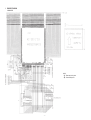
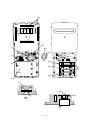
SCHEMATIC DIAGRAM
1-1. Main PCB ................................................................................................... 1
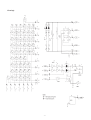
1-2. Power Supply ............................................................................................. 2
2.
SPECIFICATIONS ............................................................................................. 3
3.
OPERATION CHECK ......................................................................................... 4
4.
DATA TRANSFER CHECK ................................................................................ 8
5.
DATA COMMUNICATIONS
5-1. Connecting Two fx-9700GE Units ............................................................ 9
5-2. Before Starting Data Communications .................................................... 9
5-3. Setting Communications Parameters .................................................... 11
5-4. Using ALL, Range, and Factor................................................................ 11
5-5. Data Communications Precautions ....................................................... 13
6.
PIN FUNCTION................................................................................................. 14
7.
TROUBLESHOOTING...................................................................................... 15
8.
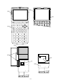
DISASSEMBLY VIEW ...................................................................................... 16
9.
PARTS LIST .................................................................................................... 21
1.
SCHEMATIC DIAGRAM
1-1. Main PCB
—1—
1-2. Power Supply
—2—
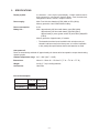
2.
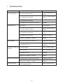
SPECIFICATIONS
Display system:
21-character × 8-line liquid crystal display; 12-digit mantissa and 2digit exponent for calculations; displays binary, octal, hexadecimal,
sexagesimal values, fraction, complex number
Power supply:
Main: Four AAA-size batteries (LR03 (AM4) or R03 (UM-4))
Memory protection: One CR2032 lithium battery
Power consumption:
0.1W
Battery life: *
Main: Approximately 650 hours with battery type LR03 (AM4)
Approximately 350 hours with battery type R03 (UM-4)
Approximately 2 years (power switch off) with LR03 (AM4)/R03
(UM-4)
Memory protection: Approximately 15 months
*
The batteries that have been installed in this unit when user pur
chased it had been used in the factory test, so it will be impossible
to fully satisfy this specifications when these batteries are used.
Auto power off:
Power is automatically switched off approximately six minutes after last operation except when drawing
dynamic graphs.
Ambient temperature range: 0°C ~ 40°C (32°F ~ 104°F)
Dimensions:
20mm H × 85mm W × 172.5mm D ( 3/4" H × 33/8" W × 63/4" D)
Weight:
218.5g (7.7 oz) including batteries
Accessories:
Hard case
Current Consumption
TYP [µA]
OFF
ON (MENU)
MAX [µA]
20.7
1430.22
2026.60
–3–
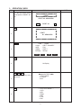
3.
OPERATION CHECK
NO.
OPERATION
Turn the side switch (LOCK)
on and push the "RESET" button.
1
DISPLAY
✽✽✽✽✽✽✽✽✽✽✽✽✽✽✽✽✽✽✽✽
✽
✽
RESET
✽✽✽✽✽✽✽✽✽✽✽✽✽✽✽✽✽✽✽✽
RESET ALL MEMORIES?
YES
F1
2
SHIFT
3
NOTE
RESET ALL
NO
✽✽✽✽✽✽✽✽✽✽✽✽✽✽✽✽✽✽✽✽
✽
✽
✽
✽
RESET
✽
✽
ALL MEMORIES!
✽
✽
✽
✽
✽
✽
✽✽✽✽✽✽✽✽✽✽✽✽✽✽✽✽✽✽✽✽
RUN
G-type
angle
display
M-D/Cpy
ZOOM
/ COMP
: RECT / CONNECT
: Deg
: Norm 1
: M-Disp
PLOT
LINE
CLS
AC
No Display
4
F6 ab/c AC
Press the above key at the
same time.
5
1
6
✽ ✽ ✽ Lx370 TEST ✽ ✽ ✽
1. TEST MODE
2. Transmit
3. Exit
– – Lx370 TEST MODE – –
1. LCD
2. KEY
3. RAM
4. DET
5. TRS
0. Rst
–4–
NO.
OPERATION
DISPLAY
1
7
FRAME Display
EXE
8
No Display
EXE
9
ALL DOT Display
EXE
10
CHECKER Display
EXE
11
REVERSE CHECKER Display
EXE
12
– – Lx370 TEST MODE – –
1. LCD
2. KEY
3. RAM
4. DET
5. TRS
0. Rst
–5–
NOTE
NO.
OPERATION
DISPLAY
2
NOTE
Trace
13
Trace Zoom
F1
F2 ........................... .
............................ EXP
ZOOM...
Press each key
sequentially as it
appears on the
display.
(–)
14
EXE
15
3
– – Lx370 TEST MODE – –
1. LCD
2. KEY
3. RAM
4. DET
5. TRS
0. Rst
RAMSIZE 32K bytes
16
RAMSIZE 32K bytes
RAM OK
EXE
17
– – Lx370 TEST MODE – –
1. LCD
2. KEY
3. RAM
4. DET
5. TRS
0. Rst
–6–
After a few
seconds.
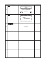
NO.
OPERATION
0
DISPLAY
NOTE
✽✽✽✽✽✽✽✽✽✽✽✽✽✽✽✽✽✽✽✽
✽
✽
RESET
✽✽✽✽✽✽✽✽✽✽✽✽✽✽✽✽✽✽✽✽
RESET ALL MEMORIES?
18
YES
RESET ALL
NO
F1
✽✽✽✽✽✽✽✽✽✽✽✽✽✽✽✽✽✽✽✽
✽
✽
✽
✽
RESET
✽
✽
ALL MEMORIES!
✽
✽
✽
✽
✽
✽
✽✽✽✽✽✽✽✽✽✽✽✽✽✽✽✽✽✽✽✽
19
SHIFT
AC
20
No Display
–7–
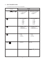
4.
DATA TRANSFER CHECK
• Turn off both units and connect them by using SB-60.
Function
b
1) Press the F6 , a /c and AC key
at the same time.
Display
Master
Slave
✽ ✽ ✽ Lx370 TEST ✽ ✽ ✽
1. TEST MODE
2. Transmit
3. Exit
✽ ✽ ✽ Lx370 TEST ✽ ✽ ✽
1. TEST MODE
2. Transmit
3. Exit
2) 1
– – Lx370 TEST MODE – –
1. LCD
2. KEY
3. RAM
4. DET
5. TRS
0. Rst
– – Lx370 TEST MODE – –
1. LCD
2. KEY
3. RAM
4. DET
5. TRS
0. Rst
3) 5
= = = TRANSMIT Check = = =
1. COM Check
2. RANDOM Data Out
= = = TRANSMIT Check = = =
1. COM Check
2. RANDOM Data Out
4) 1
0. Self
1. Send
2. Receive
5) Slave: 2
Master: 1
COM END
0. Self
1. Send
2. Receive
WAITING
COM OK
–8–
5.
DATA COMMUNICATIONS
This chapter tells you everything you need to know to transfer programs between the fx-9700GH and another
CASIO Power Graphic unit (fx-7700GB, fx-7700GE, fx-7700GH, fx-8700GB, fx-9700GE, fx-9700GH),
connected with an optionally available SB-62 cable. To transfer data between an fx-9700GH unit and a
personal computer, you will need to purchase the separately available CASIO FA-121 Ver. 2.0 Interface Unit.
This chapter also contains information on how to use the optional SB-62 cable to connect to a CASIO Label
Printer to transfer screen data for printing.
• Though you can transfer programs between the fx-9700GH and another fx-9700GH, an fx-7700GB, an fx7700GE, an fx-7700GH, an fx-8700GB or fx-9700GE, all of the examples in this manual cover data transfer
with another fx-9700GH only.
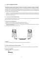
5-1. Connecting Two fx-9700GH Units
The following procedure describes how to connect two Power Graphic units with an optional SB-62 connecting
cable for transfer of programs between them.
To Connect Two fx-9700GH Units
1. Check to make sure that the power of both fx-9700GH units is off.
2. Remove the covers from the connectors of the two Power Graphic units.
• Be sure you keep the connector covers in a safe place so you can replace them after you finish your
program communications.
3. Connect the two units using the SB-62 cable.
SB-62 cable
Important
• Keep the connectors of the fx-9700GH covered when you are not using them.
5-2. Before Starting Data Communications
Before actually starting data communications, you should first enter the LINK Mode from the Main Menu.
To Enter the LINK Mode
Highlight the LINK icon on the Main Menu.
MENU
–9–
Press
to display the LINK Mode.
EXE
COMMUNICATION
EXE
PARITY : EVEN
BPS
: 9600
F1: TRANSMIT
F2: RECEIVE
F3: PARAMETERS
TRN RCV
F1
PRM
F2
F6
The following are the operations that can be selected from the function menu at the bottom of the display, Press
the function key below the operation you want to perform.
F1 (TRN) ............. Transmit
F2 (RCV) ............. Receive
F6 (PRM) ............. Parameter settings
About the Data Type Selection Screen
Whenever you press F1 (TRN) to send data or
on the display.
F2
(RCV) to receive data, a data type selection screen appears
Send Unit
F1
(TRN)
Receive Unit
F2
TRANSMIT DATA
ALL
Program
Editor
Function Memory
Matrix
Statistics
Variable Memory
Pointer
(RCV)
RECEIVE DATA
ALL
Program
Editor
Function Memory
Matrix
Statistics
Variable Memory
Indicates more below
The following table describes what each of these items means. You will learn later how to make a selection
using these screens.
Selection
ALL
Program
Editor
Function Memory
Matrix
Statistics
Variable Memory
Range
Factor
Table
Graph Function
Dynamic Graph
Equation
Back Up
Meaning
All data from Program to Equation
Program data
File names and file data
Function memory contents
Matrix memory contents
Single-variable and paired-variable statistical data
Value memory and extended memory contents
Graph range parameters
Factor function zoom ratios
Table & Graph function data
Graph functions
Dynamic Graph function data
Equation coefficients
All memory contents, including mode settings
Note
• If the selections you make on the send unit and receive unit do not match, a TRANSMIT ERROR will be
generated on the sender and a RECEIVE ERROR will be generated on the receiver.
– 10 –
5-3. Setting Communications Parameters
Before you can perform data communications, you must first set up cartain hardware parameters to make sure
that the two units are able to understand each other. The parameters of the sender and the receiver must be
identical for them to be able to communicate correctly. There are two hardware parameters that you can set.
Parameter
PARITY
Speed (BPS)
Settings
EVEN
ODD
NONE
1200
2400
4800
9600
To Set fx-9700GH Parameters
Starting from the LINK Mode:
F6
(PRM)
PARAMETERS
PARITY
EVEN ODD NONE
BPS
1200 2400 4800 9600
TO SELECT : [ ] [ ]
[ ] [ ]
TO SET
: [ EXE ]
Pointer
* The parameters that are currently set are highlighted on the display.
The pointer indicate which parameter you can change. Use
the parameter where the pointer is located.
and
to move the highlighting and change
PARAMETERS
PARITY
EVEN ODD NONE
BPS
1200 2400 4800 9600
TO SELECT : [ ] [ ]
[ ] [ ]
TO SET
: [ EXE ]
Use
and
to move the pointer up and down.
After the parameters and highlighted the way you want, press
EXE
to store them.
COMMUNICATION
EXE
PARITY : NONE
BPS
: 9600
• To abort the parameter setting procedure and return the settings to what they were before you changed
them, press AC before pressing EXE to store the parameters.
5-4. Using ALL, Range, and Factor
The following procedures show how to send data using ALL, Range, and Factor from one fx-9700GH unit
to another. The example procedure shows an operation using ALL only, but the procedures for Range
and Factor are identical.
– 11 –
• To send data using ALL
Send Unit
Receive Unit
Starting from the LINK Mode, press the function key
to enter the send mode.
Starting from the LINK Mode, press the function key
to enter the receive mode.
(TRN)
F1
F2
TRANSMIT DATA
ALL
Program
Editor
Function Memory
Matrix
Statistics
Variable Memory
Make sure that the pointer is located at ALL, and
press EXE to specify it as the data type.
EXE
(RCV)
Make sure that the pointer is located at ALL, and
press EXE to specify it as the data type.
EXE
= = RECEIVE = =
ALL
= = TRANSMIT = =
ALL
YES
NO
YES
NO
F1
F6
F1
F6
Press F1 (YES) to start the send operation, or
(NO) to abort without sending anything.
F1
RECEIVE DATA
ALL
Program
Editor
Function Memory
Matrix
Statistics
Variable Memory
(YES)
Press F1 (YES) to start the receive operation, or
(NO) to abort without receiving anything.
F6
F1
= = TRANSMITTING = =
ALL DATA
TO STOP
(YES)
F6
= = RECEIVING = =
ALL DATA
: [ AC ]
TO STOP
: [ AC ]
* Pressing AC interrupts the send operation and
returns to the LINK Mode.
* Pressing AC interrupts the receive operation and
returns to the LINK Mode.
The following appears after the send operation is
complete.
The following appears after the receive operation is
complete.
* Press
AC
COMMUNICATION
COMPLETE
ALL DATA
COMMUNICATION
COMPLETE
ALL DATA
PRESS [ AC ]
PRESS [ AC ]
to return to the LINK Mode.
Warning!
Transferring data using ALL causes data in the applicable memory areas of the receiving unit to be replaced
by the received data. Make sure that you do not need the data stored in the receiving unit before you start an
operation using ALL.
– 12 –
5-5. Data Communications Precautions
Note the following precautions whenever you perform data communications.
• A TRANSMIT ERROR occurs whenever you try to send data to a receiving unit that is not yet standing by
to receive data. When this happens, press AC to clear the error and try again, after setting up the receiving
unit to receive data.
• A RECEIVING ERROR occurs whenever the receiving unit does not receive any data approximately six
minutes after it is set up to receive data. When this happens, press AC to clear the error.
• A TRANSMIT ERROR or RECEIVE ERROR occurs during data communications if the cable becomes
disconnected, if the parameters of the two units do not match, or if any other communications problem
occurs. When this happens, press AC to clear the error and correct the problem before trying data
communications again. In this case, any data received before the problem occurred is cleared from the
receiving unit's memory.
• A MEMORY FULL operation occurs if the receiving unit memory becomes full during data communications.
When this happens, press AC to clear the error and delete unneeded data from the receiving unit to make
room for the new data, and then try again.
– 13 –
6.
PIN FUNCTION
CPU (HWD62096A03)
Pin No.
Pin Name
1
2
3
4
5
6
7
8
9
10
11,12
13
14~25
26~33
34
35
36
37
38
39~50
51
52,53
54
55~60
61
62
63~69
70~77
78~85
86
87,88
89
90,91
92
93
94~221
222~285
286
287
288~291
292~296
297
298~301
302
VSS
VREG5
VREG4
VREG2
VDT1I
VDT2A
VDT2b
VREG1
VREG3
VCC
TS1,TS2
SW
KO1~KO12
KI1~KI8
ITO
RXD
TXD
OPTO
BUFON
AO6~AO17
VSS
BZZ1,BZZ2
VSS
AO0~AO5
OEBO
WEBO
CS4BO~CS10BO
IO0~IO7
PORT0~PORT7
DUMMY
PI,PO
VSSL
XO,XI
DUMMY
VSSR
S1~S128
C1~C64
DUMMY
VLCD
V1~V4
VOL0~VOL4
DUMMY
VD1~VD4
VDB
Input / Output
I
O
I
I
I
O
I
I
I
O
O
O
O
O
O
O
O
O
I/O
I/O
O
O
– 14 –
Function
Power supply for LSI, GND
Regulator power, +5V
Regulator power for ROM, +3V
Regulator power, +2V
Terminal for detector (All off)
Terminal for detector (Lower battery)
Terminal for detector (Lower battery)
Regulator power, +3.2V
Regulator power for RAM, +3V
Power supply for LSI, +6V
Terminal for test
Reset switch
Terminal for key output
Terminal for key input
Terminal for interrupt
Terminal for communication
Terminal for communication
Output terminal
Output terminal
Address bus
Power supply for LSI, GND
Terminal for buzzer
Power supply for LSI, GND
Address bus
Output enable terminal
Write enable terminal
Chip selecter terminal
Data bus
Input/output port
Dummy terminal
Power for ceramic oscillator
Power supply for LSI, GND
Power
Dummy terminal
Power supply for LSI, GND
Terminal for LCD
Terminal for LCD
Dummy terminal
Power supply for LCD, +12V
Power supply for LCD bias
Power supply for LCD contrast
Dummy terminal
Power for doubler
Power for doubler, +12V
7.
TROUBLESHOOTING
SYMPTOM
Intermittent display
No display at all
Erratic display
Certain key does not
function
All keys do not function
Heavy key motion
CAUSE
SOLUTION
Dirt or poor contact on battery
Clean or adjust pressure of
contact
Poor contact on power switch
Clean or replace power
switch
Poor connection on PC joiner
Resolder or replace
Poor soldering on LSI, capacitor, or resistor
Resolder
Weak battery
Replace battery
Dirt or poor contact on battery
Clean or adjust pressure of
contact
Poor contact on power switch
Clean or replace power
switch
Poor connection on PC joiner
Resolder or replace
Defective LSI, capacitor, or resistor
Replace
Poor contact between LCD and PCB
Replace the heat seal
Poor soldering on LSI
Resolder or replace display
PCB ass'y
Dirt on key contact
Clean or replace contact
Heavy key motion
Clean or replace the key
Poor soldering on LSI
Resolder
Defective LSI, capacitor, or resistor
Replace
Constant contact is made on a certain key
Separate the contact
Defective LSI, capacitor, or resistor
Replace
Dirt or scratch on the key
Clean or replace the key
– 15 –
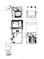
8.
DISASSEMBLY VIEW
A
7
6
9
5
0
2
B
8
4
1
3
O
T
– 16 –
GH
KL
N
CR2032
P
LOCK
QR
©™
CD
EF
IJ
B
R
+
M
S
– 17 –
CR2032
LOCK
de
XY
k
fg
B
A
B
A
no
(–)
W
(–)
Z[
j
bc
`
a
\]
UV
k
lm
B-B
hi
p
A-A
– 18 –
wx
st
uv
qr
£§
~å
†¢
ç
©™
– 19 –
y
{
z
|
ç
•¶
}
ß®
æø
¥µ
æø
º
– 20 –
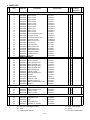
9. PARTS LIST
N
N
N
Item
Code No.
1
2
3
4
5
6
7
8
9
10
11
12
13
15
17
19
21
23
24
25
26
27
29
30
31
33
34
36
38
40
42
44
46
48
50
51
52
54
56
57
59
61
63
65
66
67
68
69
Notes:
N
M
R
Q
Parts Name
Specification
COMPONENTS
6407 9860 Button A-L370
6407 9920 Button B-L370
6408 0030 Button C-L370
6407 9870 Button D-L370
6408 0070 Button E-L370
6408 0080 Button F-L370
6408 0000 Button G-L370
6407 9970 Button H-L370
6407 9980 Button I-L370
6407 9990 Button J-L370
6408 0020 Button K-L370
6407 9880 Key contact rubber L370
6407 9930 Flat screw A-L370
6405 8860 Decoration screw C-L373
6407 9940 Flat screw C-L370
6407 9961 Battery cover L375
6405 8780 Tape E-L373
6407 9900 Hard case L370
6407 9910 Battery cover L370
6413 5800 Display plate L370
6408 0060 Battery holder L370
6408 9920 Label A-L370AHQ
6408 0220 Rubber foot L375
6390 0431 Cap V332
LOWER CASE ASS'Y
6407 9850 Lower case L370
6408 0040 Switch knob L370
6408 0010 Battery spring A-L375
6407 9950 Battery spring B-L375
6408 0100 Battery spring A-L370
6408 0110 Battery spring B-L370
6408 0120 Battery spring L370
6408 0170 Cushion A-L370
6408 0091 Battery spring A-L375
6405 9260 Nut L373
6274 7023 Contact spring
6391 8831 Reset key V160
6405 9250 Insuration seal L373
6405 9240 Battery insuration plate L373
6405 6440 Blind L171
UPPER CASE ASS'Y
6407 9840 Upper case L370
6408 0140 Adhesive tape A-L370
6408 0170 Cushion A-L370
6408 0180 Cushion B-L370
L370-1 ASS'Y
5610 7640 Heat seal A-L370
5610 7650 Heat seal B-L370
3335 4375 LCD
6407 9890 LCD holder L370
6408 0271 COF3001-F1 sub ass'y
– New parts
– Minimum order/supply quantity
– Rank
– Quantity used per unit
— 21 —
Q M
FOB Japan
N.R.Yen
R
Unit Price
A211169-1
A211316-1
A312937-1
A211172-1
A313257-1
A313257-2
A311693-9
A311693-10
A311693-11
A311693-12
A312914-1
A211181-1
A310044-41
A412299-6
A310044-43
A310945A-3
A411085-3
A211187-1
A211188-1
A312942-3
A312944-1
A413640-3
A413646-1
A310765A-1
1
1
1
1
1
1
1
1
1
1
1
1
5
1
5
1
1
1
1
1
1
1
1
1
10
10
20
20
20
20
20
20
20
20
10
5
50
50
50
10
10
5
20
5
20
20
20
10
C
C
C
C
C
C
C
C
C
C
C
C
C
C
C
C
X
C
C
C
C
X
X
B
A110736-1
A312941-1
A311808-3
A310154-3
A410112-3
A410113-3
A412218-2
A413632-1
A33938-3
A411430-3
A4532C-1
A311024A-1
A413730-1
A413729-1
A413625-1
1
1
1
1
1
2
1
4
1
1
2
1
1
1
1
1
20
10
10
20
10
10
20
20
20
10
20
10
10
10
C
C
C
C
C
C
C
C
C
X
C
C
X
C
C
A110735-1
A413594-1
A413632-1
A413633-1
1
1
1 10
1 20
1 20
C
C
C
C
A312896-1
A312898-1
CD755-TS
A211185-1
A313284A*1
R–A:
B:
C:
X:
1
A
1
1
A
1
1
A
1
C
1 20
1
B
1
Essential
Stock recommended
Others
No stock recommended
N
Item
70
72
73
75
77
79
IC1
IC2
N
IC3
IC4
X1
R1
R2
R3
R5
R6
R7
R8
R9
R10
R11
R12,13,15,16
R14
C1,C4~9
C2,C3
C10~13
C14,15
C18
86
N
81
2
2
1
1
2
1
1
1
1
1
1
1
1
1
1
1
1
1
1
1
1
4
1
7
2
4
2
1
1
20
10
50
20
20
10
1
1
1
1
5
20
20
20
20
20
20
20
10
20
20
20
20
10
10
20
20
20
1
A110886F*3
1
1
B
A413597-1
HSJ1169-012010
ECE-A1AKA2201
RH5VL40CA-T1
TC4049BF-TP1
DTC114YKT-146
MA998-(TX)
MA713-TX
MCR10EZHJ182
MCR10EZHJ473
MCR10EZHJ102
1
1
1
1
1
1
1
1
1
1
1
20
5
20
10
1
20
10
10
20
20
20
X
X
C
C
C
C
C
C
C
C
C
PCB L370-2 Ass'y
A211346A*1
1
1
B
EMI Label Z556
Label B-L370AHW
Label B-L370AHQ
Label D-L370AHQ
Label C-L370AHQ
A440515-1
A415138-2
A415138-1
A414829-2
A440517-1
1
1
1
1
1
20
20
20
20
20
X
X
X
X
X
Parts Name
6408 0150
6403 9331
6407 9930
6408 0190
6405 9110
6408 0210
2189 2009
2105 1533
2011 9891
2011 3955
2590 1561
2792 0756
2795 3213
2795 3836
2795 0693
2795 3269
2795 2443
2795 3339
3122 2009
2792 0209
2792 0845
2795 0273
2795 0525
2845 1925
2845 3486
2845 1540
2845 2499
2845 1547
6408 8020
Tape A-L370
Tape C-L170
Flat screw A-L370
Tape B-L370
Adhesive tape C-L373
PC joiner L370
Linear IC
CMOS IC
LSI
LSI
Ceramic oscillator
Chip resistor
Chip resistor
Chip resistor
Chip resistor
Chip resistor
Chip resistor
Chip resistor
Chip volume
Chip resistor
Chip resistor
Chip resistor
Chip resistor
Chip capacitor
Chip capacitor
Chip capacitor
Chip capacitor
Chip capacitor
PCB L370-2 Ass'y
Specification
6414 1890 PCB L370-1 Ass'y
L370-2 ASS'Y
6408 0160 Tape C-L370
3501 6538 Miniature jack
2805 8700 Electriolytic capasitor
2105 3206 CMOS IC
2101 0952 CMOS IC
2259 0959 Chip digital transistor
2390 1407 Chip diode
2390 0364 Schottky diode
2792 1191 Chip resistor
2792 0462 Chip resistor
2792 0470 Chip resistor
83
85
C16
IC5
IC6
Q1
D1
D2
R17
R18
R19
86
6408 8020
OTHERS
6414 1830
6411 7670
6411 7660
6412 2020
6414 2260
N
N
N
N
N
Notes:
A413596-1
A413108A-1
A310044-41
A413639-1
A412118A-2
A413642-1
LA5311M-TP-T1
RH5RA50AA-T1
TC531001CF-C100
UPD43256BGU-B12
CSTC4.91MGCM-TC
MCR10EZHJ563
MCR10EZHG513
MCR10EZHG203
MCR10EZHG123
MCR10EZHG622
MCR10EZHG302
MCR10EZHG152
MVR32HXBRN104
MCR10EZHJ104
MCR10EZHJ153
MCR10EZHJ823
MCR10EZHG105
MCH312F105ZP
MCH312F474ZP
MCH212F104ZK
MCH215A300JK
MCH215A101JK
A211346A*1
FOB Japan
N.R.Yen
R
Unit Price
X
X
C
X
C
C
C
C
B
B
C
C
C
C
C
C
C
C
C
C
C
C
C
C
C
C
C
C
B
Code No.
N
M
R
Q
–
–
–
–
New parts
Minimum order/supply quantity
Rank
Quantity used per unit
— 22 —
Q M
R–A:
B:
C:
X:
Essential
Stock recommended
Others
No stock recommended
8-11-10, Nishi-Shinjuku
Shinjuku-ku, Tokyo 160, Japan
Telephone: 03-3347-4926