1
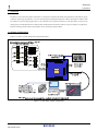
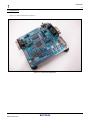
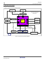
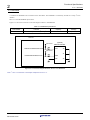
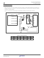
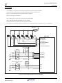
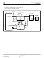
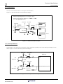
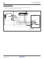
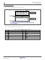
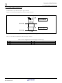
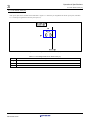
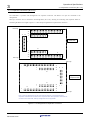
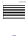
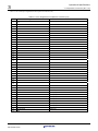
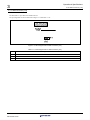
To our customers,
Old Company Name in Catalogs and Other Documents
On April 1st, 2010, NEC Electronics Corporation merged with Renesas Technology
Corporation, and Renesas Electronics Corporation took over all the business of both
companies. Therefore, although the old company name remains in this document, it is a valid
Renesas Electronics document. We appreciate your understanding.
Renesas Electronics website: http://www.renesas.com
April 1st, 2010
Renesas Electronics Corporation
Issued by: Renesas Electronics Corporation (http://www.renesas.com)
Send any inquiries to http://www.renesas.com/inquiry.
Notice
1.
2.
3.
4.
5.
6.
7.
All information included in this document is current as of the date this document is issued. Such information, however, is
subject to change without any prior notice. Before purchasing or using any Renesas Electronics products listed herein, please
confirm the latest product information with a Renesas Electronics sales office. Also, please pay regular and careful attention to
additional and different information to be disclosed by Renesas Electronics such as that disclosed through our website.
Renesas Electronics does not assume any liability for infringement of patents, copyrights, or other intellectual property rights
of third parties by or arising from the use of Renesas Electronics products or technical information described in this document.
No license, express, implied or otherwise, is granted hereby under any patents, copyrights or other intellectual property rights
of Renesas Electronics or others.
You should not alter, modify, copy, or otherwise misappropriate any Renesas Electronics product, whether in whole or in part.
Descriptions of circuits, software and other related information in this document are provided only to illustrate the operation of
semiconductor products and application examples. You are fully responsible for the incorporation of these circuits, software,
and information in the design of your equipment. Renesas Electronics assumes no responsibility for any losses incurred by
you or third parties arising from the use of these circuits, software, or information.
When exporting the products or technology described in this document, you should comply with the applicable export control
laws and regulations and follow the procedures required by such laws and regulations. You should not use Renesas
Electronics products or the technology described in this document for any purpose relating to military applications or use by
the military, including but not limited to the development of weapons of mass destruction. Renesas Electronics products and
technology may not be used for or incorporated into any products or systems whose manufacture, use, or sale is prohibited
under any applicable domestic or foreign laws or regulations.
Renesas Electronics has used reasonable care in preparing the information included in this document, but Renesas Electronics
does not warrant that such information is error free. Renesas Electronics assumes no liability whatsoever for any damages
incurred by you resulting from errors in or omissions from the information included herein.
Renesas Electronics products are classified according to the following three quality grades: “Standard”, “High Quality”, and
“Specific”. The recommended applications for each Renesas Electronics product depends on the product’s quality grade, as
indicated below. You must check the quality grade of each Renesas Electronics product before using it in a particular
application. You may not use any Renesas Electronics product for any application categorized as “Specific” without the prior
written consent of Renesas Electronics. Further, you may not use any Renesas Electronics product for any application for
which it is not intended without the prior written consent of Renesas Electronics. Renesas Electronics shall not be in any way
liable for any damages or losses incurred by you or third parties arising from the use of any Renesas Electronics product for an
application categorized as “Specific” or for which the product is not intended where you have failed to obtain the prior written
consent of Renesas Electronics. The quality grade of each Renesas Electronics product is “Standard” unless otherwise
expressly specified in a Renesas Electronics data sheets or data books, etc.
“Standard”:
8.
9.
10.
11.
12.
Computers; office equipment; communications equipment; test and measurement equipment; audio and visual
equipment; home electronic appliances; machine tools; personal electronic equipment; and industrial robots.
“High Quality”: Transportation equipment (automobiles, trains, ships, etc.); traffic control systems; anti-disaster systems; anticrime systems; safety equipment; and medical equipment not specifically designed for life support.
“Specific”:
Aircraft; aerospace equipment; submersible repeaters; nuclear reactor control systems; medical equipment or
systems for life support (e.g. artificial life support devices or systems), surgical implantations, or healthcare
intervention (e.g. excision, etc.), and any other applications or purposes that pose a direct threat to human life.
You should use the Renesas Electronics products described in this document within the range specified by Renesas Electronics,
especially with respect to the maximum rating, operating supply voltage range, movement power voltage range, heat radiation
characteristics, installation and other product characteristics. Renesas Electronics shall have no liability for malfunctions or
damages arising out of the use of Renesas Electronics products beyond such specified ranges.
Although Renesas Electronics endeavors to improve the quality and reliability of its products, semiconductor products have
specific characteristics such as the occurrence of failure at a certain rate and malfunctions under certain use conditions. Further,
Renesas Electronics products are not subject to radiation resistance design. Please be sure to implement safety measures to
guard them against the possibility of physical injury, and injury or damage caused by fire in the event of the failure of a
Renesas Electronics product, such as safety design for hardware and software including but not limited to redundancy, fire
control and malfunction prevention, appropriate treatment for aging degradation or any other appropriate measures. Because
the evaluation of microcomputer software alone is very difficult, please evaluate the safety of the final products or system
manufactured by you.
Please contact a Renesas Electronics sales office for details as to environmental matters such as the environmental
compatibility of each Renesas Electronics product. Please use Renesas Electronics products in compliance with all applicable
laws and regulations that regulate the inclusion or use of controlled substances, including without limitation, the EU RoHS
Directive. Renesas Electronics assumes no liability for damages or losses occurring as a result of your noncompliance with
applicable laws and regulations.
This document may not be reproduced or duplicated, in any form, in whole or in part, without prior written consent of Renesas
Electronics.
Please contact a Renesas Electronics sales office if you have any questions regarding the information contained in this
document or Renesas Electronics products, or if you have any other inquiries.
(Note 1) “Renesas Electronics” as used in this document means Renesas Electronics Corporation and also includes its majorityowned subsidiaries.
(Note 2) “Renesas Electronics product(s)” means any product developed or manufactured by or for Renesas Electronics.
User’s Manual
SH7137 CPU Board
M3A-HS37
User’s Manual
Renesas 32-Bit RISC Microcomputer
SuperH RISC engineFamily/SH7137 Group
Rev.1.00 2008.10
Table of Contents
Chapter 1 Overview ............................................................................................................................. 1-1
1.1 Overview................................................................................................................................................................... 1-2
1.2 U System Configuration ............................................................................................................................................... 1-2
1.3 U External Specifications ............................................................................................................................................. 1-3
1.4 U Appearance .............................................................................................................................................................. 1-4
1.5 U M3A-HS37 Block Diagram ........................................................................................................................................ 1-5
1.6 U M3A-HS37 Major Components ................................................................................................................................. 1-6
1.7 U M3A-HS37 Memory Map .......................................................................................................................................... 1-8
1.8 U Absolute Maximum Ratings .................................................................................................................................... 1-10
1.9 U Recommended Operating Conditions ..................................................................................................................... 1-10
Chapter 2 Functional Specifications .................................................................................................... 2-1
2.1 Features ..................................................................................................................................................................... 2-2
2.2 CPU............................................................................................................................................................................ 2-3
2.3 Memory ...................................................................................................................................................................... 2-4
2.3.1 SH7137 Internal Memory .................................................................................................................................. 2-4
2.3.2 SRAM................................................................................................................................................................ 2-4
2.3.3 EEPROM........................................................................................................................................................... 2-5
2.4 Serial Port Interface.................................................................................................................................................... 2-6
2.5 I/O Ports ..................................................................................................................................................................... 2-7
2.6 Power Supply Module............................................................................................................................................... 2-10
2.7 RCAN Interface ........................................................................................................................................................ 2-11
2.8 Clock Modules.......................................................................................................................................................... 2-12
2.9 Reset Module ........................................................................................................................................................... 2-13
2.10 Interrupt Switches................................................................................................................................................... 2-13
2.11 E10A-USB Interface ............................................................................................................................................... 2-14
Chapter 3 Operational Specifications .................................................................................................. 3-1
3.1 M3A-HS37 Connectors............................................................................................................................................... 3-2
3.1.1 H-UDI Connector (J2) ....................................................................................................................................... 3-3
3.1.2 Serial Port Connector (J3)................................................................................................................................. 3-4
3.1.3 Power Supply Connector (J4) ........................................................................................................................... 3-5
3.1.4 External Power Supply Connectors for SH7137 (J5, J6, and J16) .................................................................... 3-6
3.1.5 DC Power Jack (J7) .......................................................................................................................................... 3-7
3.1.6 Expansion Connectors (J8 to J12) .................................................................................................................... 3-8
3.1.7 RCAN Connector (J13) ................................................................................................................................... 3-14
3.1.8 GND Connector (J15) ..................................................................................................................................... 3-15
3.2 Switches and LEDs .................................................................................................................................................. 3-16
3.2.1 CPU Power Supply Select Jumper (JP1) ........................................................................................................ 3-17
3.2.2 External Power Supply Select Jumpers (JP2, JP3, and JP4).......................................................................... 3-18
3.2.3 Serial Port/SRAM Select Jumpers (JP7 to JP11), RCAN-I/O Jumpers (JP12, and JP13) .............................. 3-19
3.2.4 Switches and LEDs ......................................................................................................................................... 3-20
3.2.5 Jumper Switch Setting when Using Development Tool ................................................................................... 3-22
Rev.1.00 Oct 09, 2008
REJ11J0021-0100
(i)
3.3 M3A-HS37 Dimensions ............................................................................................................................................ 3-23
Appendix..............................................................................................................................................A-1
M3A-HS37 SCHEMATICS
Rev.1.00 Oct 09, 2008
REJ11J0021-0100
(ii)
Chapter 1
1-1
Overview
Chapter 1
Overview
Overview
1
1.1 Overview
1.1 Overview
The SH7137 CPU board (Part number: M3A-HS37) is designed for evaluating the feature and performance of the SH7137 group
of Renesas Technology original MCU, as well as developing and evaluating the application software for the MCUs. SH7137 data
bus, address bus and on-chip peripheral pins are all connected to the expansion connectors on the M3A-HS37 to allow for the
timing analysis with peripherals that use measurement instruments and connections of MCU I/O pins according to its application.
Renesas Technology E10A-USB on-chip emulator can be connected to the M3A-HS37.
1.2 System Configuration
U
Figure 1.2.1 shows a system configuration using the M3A-HS37.
3
2
1
ON
4
2H
Figure 1.2.1 M3A-HS37 System Configuration
Rev.1.00 Oct 09, 2008
REJ11J0021-0100
1-2
Overview
1
1.3 External Specifications
U
1.3 External Specifications
U
Table 1.3.1 list the M3A-HS37 external specifications.
3H
Table 1.3.1 External Specifications
No.
Item
Description
SH7137
1
CPU
z
Input (XIN) clock: 10.0 MHz
z
CPU clock: 80 MHz (max.)
z
Bus clock: Maximum 40 MHz (max.)
z
On-chip memory
• Flash memory: 256 KB
• RAM: 16 KB
z
2
Memory
SRAM: 32 KB
M5M5256DFP-70GI: 1 (8-bit bus width, optional)
z
EEPROM: 16 KB (optional)
HN58X24128FPIE: 1 (I2C bus connection)
P
3
4
5
6
Connectors
LEDs
Switches
Dimensions
Rev.1.00 Oct 09, 2008
REJ11J0021-0100
P
z
Expansion connectors (Bus, I/O, VCC, and GND)
z
Serial port connector (D-sub 9-pin)
z
H-UDI connector (14-pin)
z
RCAN connector (D-sub 9-pin)
z
POWER LED: 1
z
User LEDs: 6
z
Reset switch: 1
z
NMI switch: 1
z
IRQ2 switch: 1
z
System setting DIP switches: 4/package
z
User DIP switches: 4/package
z
Dimensions: 100 mm x 100 mm
z
Mounting form : 4 layers, double-sided
z
Board configuration : 1 board
1-3
Overview
1
1.4
U
1.4 Appearance
U
Figure 1.4.1 shows the M3A-HS37 appearance.
4H
Figure 1.4.1 M3A-HS37 Appearance
Rev.1.00 Oct 09, 2008
REJ11J0021-0100
1-4
Overview
1
1.5 M3A-HS37 Block Diagram
U
1.5 M3A-HS37 Block Diagram
U
Figure 1.5.1 shows the M3A-HS37 system block diagram.
5H
Serial port
connector
H-UDI connector
(14-pin)
SH7137 CPU board
M3A-HS37
RS-232C driver
H-UDI
RCAN connector
(D-Sub 9-pin)
RCAN driver
SCI
RCAN
SH7137
(80 MHz)
PIO
Six user LEDs
INTC
NMI
switch
INTC
IRQ2
switch
ADC
A/D connector
PIO
16
16
I2C
BSC
8
4
External bus
Maximum 40 MHz
8
DIP switches
(4/package)
EEPROM
(16 KB)
SRAM
(32 KB)
Expansion connector
: Optional
Figure 1.5.1 M3A-HS37 System Block Diagram
Rev.1.00 Oct 09, 2008
REJ11J0021-0100
1-5
Overview
1
1.6
U
M3A-HS37 Major Components
1.6 M3A-HS37 Major Components
U
6H
Figure 1.6.1 shows the M3A-HS37 major components.
Top view of the component side
J15
GND connector
(optional)
JP11
PE10/CS0#
jumper
LED1
Power LED
J4
SW1
Power
System power
supply
on/off switch
connector
U9
3.3V Regulator
U12
RCAN
driver
U4
EEPROM
(optional)
J13
RCAN
port connector
J7
DC Power jack
JP1
CPU power supply select
jumper
JP2 to JP4
External power
switch jumpers
J3
Serial port
connector U5
SRAM
(optional)
JP12,JP13
RCAN port jumpers
JP7 to JP10
Serial port
switch jumpers
RS-232C
driver
U1
SH7137
LED2 to LED7
User LEDs
J2
H-UDI connector
(14-pin)
SW2
Reset
switch
SW4
System setting
DIP switches
SW3
User DIP
switches
SW6
IRQ2 switch
J5,J6, and J16
External power
supply connectors
(optional)
SW5
NMI switch
Top view of the solder side
Figure 1.6.1 M3A-HS37 Major Components
Rev.1.00 Oct 09, 2008
REJ11J0021-0100
1-6
Overview
1
1.6
U
M3A-HS37 Major Components
Table 1.6.1 lists the major components on the M3A-HS37.
7H
Table 1.6.1 Main Components Mounted on the M3A-HS37
No.
Name
Part Number
Manufacturer
Remarks
U1
CPU
SH7137
Renesas
U1
CPU socket
NQPACK100SD(-ND)
TET
U2
SRAM
M5M5256DFP-70GI
Renesas
Optional
U4
EEPROM
HN58X24128FPIE
Renesas
Optional
U5
RS-232C driver
SP3232ECA
Sipex
U6
Reset IC
M51957BFP
Renesas
U9
3.3 V regulator
LM2738YMY
NS
U10
Inverter
HD74LV2G14A
Renesas
U11
Inverter
SN74LVC14APWR
TI
U12
RCAN driver IC
HA13721FPK
Renesas
U13, U14
Level shifters
SN74VC2T45DCT
TI
X1
Oscillator
SG8002DC_10.0MHz
Epson
X1
Oscillator socket
X2
Oscillator
CX5032GB 10000
KYOCERA KINSEKI
J2
H-UDI connector (14-pin)
7614-6002
Sumitomo 3M
J3
Serial port connector
XM2C-0942-132L
OMRON
J4
Power supply connector
S2B-XH-A
JST
J7
DC power jack
HEC0470-01-630
HOSIDEN
J8, J10, J11
Expansion connectors (20-pin)
XG8T-2031
OMRON
Optional
J9, J12
Expansion connectors (40-pin)
XG8T-2031: 2
OMRON
Optional
J13
CAN connector (9-pin)
XM2C-0942-132L
OMRON
LED1
Power LED
Blue
LED2 to LED7
User LEDs
Green
SW1
Power switch
MS-12AAH1
nikkai
SW2
Reset switch
B3SN-3012
OMRON
Push-button switch
SW3
User DIP switches
A6S-4104
OMRON
4/package
SW4
System setting DIP switches
A6S-4104
OMRON
4/package
SW5
NMI switch
B3SN-3012
OMRON
Push-button switch
SW6
IRQ2 switch
B3SN-3012
OMRON
Push-button switch
Rev.1.00 Oct 09, 2008
REJ11J0021-0100
SW regulator
Optional
Optional
1-7
Overview
1
1.7 M3A-HS37 Memory Map
U
1.7 M3A-HS37 Memory Map
U
Figure 1.7.1 and Figure 1.7.2 show the memory map examples of SH7137 on the M3A-HS37.
8H
9H
SH7137 logical space
MCU Mode 3
(Single chip mode)
H'0000 0000
M3A-HS37
Memory Map
H'0000 0000
On-chip ROM (256 KB)
On-chip ROM (256 KB)
H'0003 FFFF
H'0004 0000
H'0003 FFFF
H'0004 0000
Reserved
Reserved
H'FFFF 7FFF
H'FFFF 8000
H'FFFF 7FFF
H'FFFF 8000
On-chip RAM (16 KB)
On-chip RAM (16 KB)
H'FFFF BFFF
H'FFFF C000
H'FFFF BFFF
H'FFFF C000
Peripheral I/O
H'FFFF FFFF
Peripheral I/O
H'FFFF FFFF
Figure 1.7.1 SH7137 Memory Map (MCU mode 3)
Rev.1.00 Oct 09, 2008
REJ11J0021-0100
1-8
Overview
1
1.7 M3A-HS37 Memory Map
U
SH7137 logical space
MCU mode 2
(On-chip ROM enable mode)
H'0000 0000
M3A-HS37
Memory Map
H'0000 0000
On-chip ROM (256 KB)
On-chip ROM (256 KB)
H'0003 FFFF
H'0004 0000
H'0003 FFFF
H'0004 0000
Reserved
H'01FF FFFF
H'0200 0000
Reserved
H'01FF FFFF
H'0200 0000
CS0 space
H'020F FFFF
H'0210 0000
H'0200
H'0200
H'020F
H'0210
7FFF
8000
FFFF
0000
Reserved
SRAM (32 KB) *1
User Area
Reserved
H'03FF FFFF
H'0400 0000
H'03FF FFFF
H'0400 0000
CS1 space
H'040F FFFF
H'0410 0000
User Area
H'040F FFFF
H'0410 0000
Reserved
Reserved
H'FFFF 7FFF
H'FFFF 8000
H'FFFF 7FFF
H'FFFF 8000
On-chip RAM (16 KB)
On-chip RAM (16 KB)
H'FFFF BFFF
H'FFFF C000
H'FFFF BFFF
H'FFFF C000
Peripheral I/O
H'FFFF FFFF
Peripheral I/O
H'FFFF FFFF
Note: SRAM is optional.
Figure 1.7.2 SH7137 Memory Map (MCU mode 2)
Rev.1.00 Oct 09, 2008
REJ11J0021-0100
1-9
Overview
1
1.8 Absolute Maximum Ratings
U
1.8 Absolute Maximum Ratings
U
Table 1.8.1 lists the absolute maximum ratings of the M3A-HS37.
10H
Table 1.8.1 Absolute Maximum Ratings of M3A-HS37
Symbol
CPU-VCC
Parameter
Rated Value
Remarks
Power supply voltage
-0.3 to 7.0 V
Reference voltage: VSS. Both VCC = 5 V and
3.3 V allowed.
ADC power supply voltage
AVCC
Topr
Operating temperature
Tstr
Storage temperature
-0.3 to 7.0 V
0 to 50°C
-10 to 60°C
Reference voltage: AVSS, for A/D converter
No dewdrops allowed.
No corrosion gas allowed
Note: Temperature refers to the air temperature in the vicinity of the board.
1.9 Recommended Operating Conditions
U
Table 1.9.1 lists the recommended operating conditions of the M3A-HS37.
1H
Table 1.9.1 Operating Conditions
Symbol
Parameter
CPU-VCC 3.3-5 V systems power supply voltage
Value
3.0 to 5.5 V
Remarks
Reference voltage: VSS
Both VCC = 5 V and 3.3 V allowed
AVCC
Topr
ADC power supply voltage
4.5 to 5.5 V
Maximum current consumption
1.5 A max.
Operating temperature
0 to 50°C
Reference voltage: AVSS, for A/D converter
No dewdrops allowed, no corrosion gas
allowed.
Rev.1.00 Oct 09, 2008
REJ11J0021-0100
1-10
Chapter 2Functional Specifications
Chapter 2
Functional Specifications
2-1
Functional Specifications
2
2.1 Features
2.1 Features
The M3A-HS37 CPU board has function modules listed in Table 2.1.1.
Table 2.1.1 lists the M3A-HS37 functional modules.
Table 2.1.1 M3A-HS37 Functional Modules
Section
2.2
Features
CPU
Description
SH7137
• Input (XIN) clock: 10.0 MHz
• CPU clock: 80 MHz (max.)
• Bus clock: 40 MHz (max.)
• Internal memory
• Flash memory: 256 KB
• RAM: 16 KB
2.3
Memory
• SRAM: 32 KB
M5M5256DFP-70GI: 1 (8-bit bus width, optional)
• EEPROM: 16 KB (optional)
HN58X24128FPIE: 1 (I2C bus connection)
2.4
Serial Port Interface
Connects the SH7137 SCI1 or SCI0 pins to the serial port connector
2.5
I/O Ports
Connects to the SH7137 I/O ports
2.6
Power Supply Module
Controls the M3A-HS37 system power supply
2.7
RCAN Interface
Connects the SH7137 CAN pin to RCAN connector via an RCAN driver
2.8
Clock Modules
Controls the system clock
2.9
Reset Module
Resets the device on the M3A-HS37
2.10
Interrupt Switches
Connect to the NMI pin, IRQ2 pin and test port
2.11
E10A-USB Interface
SH7137 H-UDI interface (14-pin)
Operational Specifications
Connectors, switches and LEDs
-
• SH7137 expansion connectors
• Switches and LEDs
• H-UDI connector
Refer to Chapter 3 for details.
Rev.1.00 Oct 09, 2008
REJ11J0021-0100
2-2
Functional Specifications
2
2.2 CPU
2.2 CPU
The M3A-HS37 is provided with the SH7137, the 32-bit RISC MCU operates with a maximum frequency of 80 MHz.
The SH7137 MCU is provided with a 256-KB flash memory, and a 16-KB RAM, which covers a wide range of applications
from data processing to equipment control.
The M3A-HS37 can be operated with a maximum CPU frequency of 80 MHz (external bus 40 MHz at maximum) using a 10.0
MHz of the input clock.
Figure 2.2.1 shows the SH7137 block diagram on the M3A-HS37.
SH7137
Clock
EXTAL
XTAL
PA15/CK/TXD1/SSO
Mode
SW
MD1
MD0
FWE
System
control
RES
NMI
WDTOVF
User
LEDs
PE9/TIOC3B
PE11/TIOC3D
PE12/TIOC4A
PE13/TIOC4B/MRES
PE14/TIOC4C
PE15/TIOC4D/IRQOUT
Control signal,
MTU2/2S,
interrupt,
etc
RCAN
port
Serial
port
PA9/WAIT/TCLKD/POE8/TXD2
PA8/WRL/TCLKC/POE6/RXD2
PA7/TCLKB/POE5/SCK2
PA6/RD/UBCTRG/TCLKA
PB0/BACK/TIC5WS/
PB1/BREQ/TIC5W
PB6/WAIT/CTx0
PB7/CS1/CRx0
PD8/SCK2/SSCK
PD9/SSI
PD10/SSO
PE0/TIOC0A
PE1/TIOC0B/RXD0
PE2/TIOC0C/TXD0
PE3/TIOC0D/SCK0
PE10/TIOC3C/CS0
PE12/TIOC4A
PE13/TIOC4B/MRES
PE14/TIOC4C
PE15/TIOC4D/IRQOUT
PA0/RXD0/A0/POE0
PA1/TXD0/A1/POE1
PA2/SCK0/IRQ0/A2/POE2
PA3/RXD1/A3/IRQ1
PA4/TXD1/A4/IRQ2
PA5/SCK1/A5/IRQ3
PA10/A6/RXD0
PA11/ADTRG/A7/TXD0
PA12/A8/SCS/SCK0
PA13/A9/SSCK/SCK1
PA14/A10/SSI/RXD1
PE4/TIOC1A/A11/RXD1
PE5/TIOC1B/A12/TXD1
PE6/TIOC2A/A13/SCK1
PE7/TIOC2B/A14
PE8/TIOC3A/A15
PB2/IRQ0/POE0/TIC5VS/SCL/A16
PB3/IRQ1/POE1/TIC5V/SDA/A17
PB4/IRQ2/TIC5US/A18/POE4
PB5/IRQ3/TIC5U/A19/POE5
PD0/D0/RXD0
PD1/D1/TXD0
PD2/D2/SCK0
PD3/D3/RXD1
PD4/D4/TXD1
PD5/D5/SCK1
PD6/D6/RXD2
PD7/D7/TXD2
PE18/TIOC4AS/CS1/TDI
PE19/TIOC4BS/RD/TDO
PE17/TIOC3DS/CS0/TCK
PE20/TIOC4CS//TMS
PE21/TIOC4DS/WRL/TRST
PE16/TIOC3BS/WAIT/ASEBRKAK/ASEBRK
ASMD0
PF0/AN0
PF1/AN1
PF2/AN2
PF3/AN3
PF4/AN4
PF5/AN5
PF6/AN6
PF7/AN7
PF8/AN8
PF9/AN9
PF10/AN10
PF11/AN11
PF12/AN12
PF13/AN13
PF14/AN14
PF15/1N15
Serial
port
Address bus
SRAM/
/I/O port
EEPROM
Data bus
/SRAM
/Input port
H-UDI
A/D
/Input port
User
DIP
switches
Figure 2.2.1 SH7137 Block Diagram
Rev.1.00 Oct 09, 2008
REJ11J0021-0100
2-3
Functional Specifications
2
2.3 Memory
2.3 Memory
2.3.1 SH7137 Internal Memory
The SH7137 MCU is provided with a 256-KB flash memory and a 16-KB RAM.
2.3.2 SRAM
A 32-KB of SRAM can be mounted on the M3A-HS37 (optional). Both 5 V and 3.3 V can be supplied for the CPU and the
SRAM on the M3A-HS37. The supply voltage supplied to the CPU is also supplied to SRAM. When M5M5256DFP-70GI is
mounted as SRAM, the supply voltage is automatically the same as the CPU. The SRAM is controlled by the SH7137 on-chip
bus state controller.
Table 2.3.1 lists the SRAM specifications. Figure 2.3.1 shows the block diagram of the connection between the SH7137 and
SRAM. Table 2.3.2 lists the jumper connections.
Table 2.3.1 SRAM Specifications
Part Number
Bus size
Capacity
Package
M5M5256DFP-70GI
8-bit
32 KB (bus width: 8-bit)
28-pin SOP (450 mil)
Figure 2.3.1 Connection Diagram Between SH7137 and SRAM
Table 2.3.2 Jumper Connections
SCI0
SCI1
SRAM
JP7
JP8
JP9
JP10
Y
N
Y
2-3
2-3
2-3
2-3
N
Y
N
1-2
1-2
1-2
1-2
Note: Y = yes, N = no
Rev.1.00 Oct 09, 2008
REJ11J0021-0100
2-4
Functional Specifications
2
2.3.3 EEPROM
2.3.3 EEPROM
A 16-KB of the EEPROM can be mounted on the M3A-HS37. The EEPROM is controlled by the SH7137 on-chip I2C bus
interface.
Table 2.3.3 lists the EEPROM specifications.
Figure 2.3.2 shows the connection circuit block diagram of SH7137 and EEPROM.
Table 2.3.3 EEPROM Specifications
Part Number
Interface
Capacity
Package
HN58X24128FPIE
2-wire system serial (I2C bus) *
16 KB
8-pin SOP
SH7137
CPU-VCC
(optional)
HN58X24128FPIE
0
SCL
PB2/SCL/POE0/IRQ0/TIC5VS
A0
CPU-VCC
PB3/SDA/POE1/IRQ1/TIC5V
0
A1
SDA
WP
A2
16 KB EEPROM
Figure 2.3.2 Connection Diagram Between SH7137 and EEPROM
Note: I2C bus is a trademark of Koninklijke Philips Electronics N. V.
Rev.1.00 Oct 09, 2008
REJ11J0021-0100
2-5
Functional Specifications
2
2.4 Serial Port Interface
2.4 Serial Port Interface
SH7137 SCI0 or SCI 1 pins can be connected to the serial port connector on the M3A-HS37 (default: PE1 pin and PE2 pin are
connected to the serial port connector, J3). The serial port switch jumpers (JP7, JP8, JP9, and JP10) switch the SCI channels
connected to a serial port connector.
Figure 2.4.1 shows the serial port block diagram on the M3A-HS37, and Table 2.4.1 lists the jumper connections.
Serial port
RS-232C CPU-VCC
connector
driver
1
CPU-VCC
NC
DCD
4.7 K
2
RxD
3
CPU-VCC
TxD
4.7 K
4
DTR
5
GND
6
DSR
7
RTS
8
CTS
9
NC
RI
CPU-VCC:3.3 V/ 5 V
SH7137
CPU-VCC
JP8
PA3/RXD1/A3/IRQ1
1
2
3
JP7
PA4/TXD1/A4/IRQ2
1
3
2
PE1/TIOC0B/RXD0
PE2/TIOC0C/TXD0
CPU-VCC
JP10
1
3
2
A3
A4
JP9
1
3
SRAM
(M5M5256DFP-70GI)
2
Figure 2.4.1 Serial Port Block Diagram
Table 2.4.1 Jumper Connections
SCI0
SCI1
SRAM
JP7
JP8
JP9
JP10
Y
N
Y
2-3
2-3
2-3
2-3
N
Y
N
1-2
1-2
1-2
1-2
Note: Y = yes, N = no
Rev.1.00 Oct 09, 2008
REJ11J0021-0100
2-6
Functional Specifications
2
2.5 I/O Ports
2.5 I/O Ports
All of the SH7137 I/O ports are connected to the expansion bus connectors on the M3A-HS37.
Some I/O ports are connected to the DIP switches and LEDs, which are allowed for user.
Figure 2.5.1 shows the DIP switches and LEDs connection diagram.
Table 2.5.1 lists the I/O port features.
Note: Unused ports are open to allow for expansion on the M3A-HS37.
(PA6 to PA9, PB0, PB1, PB5, PD8-PD10, PE0, PE3, and PE8)
Set these unused ports as output at first when using the M3A-HS37.
When some ports of the SH7137 MCU are unused on the user system, the pull-up or pull-down process is recommended.
CPU-VCC
SW4-4
H7
H6
H5
H4
H3
H2
LED2
Green
LED7
Green
LED6
Green
LED5
Green
LED4
Green
0
LED3
Green
0
0
0
0
0
SH7137
PE9/TIOC3B
PE11/TIOC3D
PE12/TIOC4A
PE13/TIOC4B/MRES
PE14/TIOC4C
PE15/TIOC4D/IRQOUT
CPU-VCC
User DIP
switches (SW3)
SW3-1
0
SW3-2
0
SW3-3
0
SW3-4
0
PF12/AN12
PF13/AN13
PF14/AN14
PF15/AN15
CPU-VCC
System setting DIP switches
(SW4)
SW4-1
FWE
SW4-2
MD1
SW4-3
MD2
Figure 2.5.1 DIP Switches and LEDs Connection Diagram
Rev.1.00 Oct 09, 2008
REJ11J0021-0100
2-7
Functional Specifications
2
2.5 I/O Ports
Table 2.5.1 I/O Port Features
SH7137
No.
2
4
5
6
7
8
9
10
12
13
15
17
18
19
20
21
22
23
24
25
26
27
28
29
30
31
32
33
34
35
37
38
40
41
42
43
44
45
46
47
49
51
52
53
54
55
56
58
60
61
62
63
65
66
67
68
69
Pin Name
PE21/WRL/TIOC4DS/TRST
PE20/TIOC4CS/TMS
PE19/RD/TIOC4BS/TDO
PE18/CS1/TIOC4AS/TDI
PE17/CS0/TIOC3DS/TCK
PE16/WAIT/TIOC3BS/ASEBKAK/ASEBK
PE15/TIOC4D/IRQOUT
PE14/TIOC4C
PE13/TIOC4B/MRES
PE12/TIOC4A
PE11/TIOC3D
PE9/TIOC3B
PE10/CS0/TIOC3C
PE8/A15/TIOC3A
PE7/A14/TIOC2B
PE6/A13/TIOC2A/SCK1
PE5/A12/TIOC1B/TXD1
PE4/A11/TIOC1A/RXD1
PE3/TIOC0D/SCK0
PE2/TIOC0C/TXD0
PE1/TIOC0B/RXD0
PE0/TIOC0A
PD10/SSO
PD9/SSI
PD8/SCK2/SSCK
PD7/D7/TXD2/SCS
PD6/D6/RXD2
PD5/D5/SCK1
PD4/D4/TXD1
PD3/D3/RXD1
PD2/D2/SCK0
PD1/D1/TXD0
PD0/D0/RXD0
PB7/CS1/CRx0
PB6/WAIT/CTx0
PB5/A19/IRQ3/POE5/TIC5U
PB4/A18/IRQ2/POE4/TIC5US
PB3/A17/IRQ1/POE1/TIC5V/SDA
PB2/A16/IRQ0/POE0/TIC5VS/SCL
PB1/BREQ/TIC5W
PB0/BACK/TIC5WS
PA15/CK/TXD1/SSO
PA14/A10/RXD1/SSI
PA13/A9/SCK1/SSCK
PA12/A8/SCK0/SCS
PA11/A7/TXD0/ADTRG
PA10/A6/RXD0
PA9/WAIT/TCLKD/POE8/TXD2
PA8/ /WRL/TCLKC/POE6/RXD2
PA7/TCLKB/POE5/SCK2/
PA6/RD/UBCTRG/TCLKA/POE4
PA5/A5/IRQ3/SCK1
PA4/A4/IRQ2/TXD1
PA3/A3/IRQ1/RXD1
PA2/A2/IRQ0/POE2/SCK0
PA1/A1/POE1/TXD0
PA0/A0/POE0/RXD0
Rev.1.00 Oct 09, 2008
REJ11J0021-0100
Expansion connectors
J8
J9
J10
J11
Remarks
J12
√*
√*
√*
√*
√*
√
√
√
√
√
√
√
√
√
√
√
√
√
√
√
√
√
LED
LED
LED
LED
LED
LED
Serial
Serial
√
√
√
√
√
√
√
√
√
√
√
√
√
√
√
RCAN
RCAN
√
√
√
√
IRQ2 SW
EEPROM
EEPROM
√
√
√
√
√
√
√
√
√
√
√
√
√
√
√
√
√
Serial
Serial
2-8
Functional Specifications
2
2.5 I/O Ports
SH7137
No.
Pin Name
Expansion connectors
J8
J9
J10
J11
Remarks
J12
80
PF15/AN15
√
81
PF14/AN14
√
82
PF13/AN13
√
83
PF12/AN12
√
Analog input pin
User DIP switches SW
Analog input pin
User DIP switches SW
Analog input pin
User DIP switches SW
Analog input pin
User DIP switches SW
84
PF11/AN11
√
Analog input pin
85
PF10/AN10
√
Analog input pin
86
PF9/AN9
√
Analog input pin
87
PF8/AN8
√
Analog input pin
89
PF7/AN7
√
Analog input pin
90
PF6/AN6
√
Analog input pin
91
PF5/AN5
√
Analog input pin
92
PF4/AN4
√
Analog input pin
94
PF3/AN3
√
Analog input pin
95
PF2/AN2
√
Analog input pin
96
PF1/AN1
√
Analog input pin
97
PF0/AN0
√
Analog input pin
Note: Connected only when the 0Ω resistance is mounted.
Rev.1.00 Oct 09, 2008
REJ11J0021-0100
2-9
Functional Specifications
2
2.6 Power Supply Module
2.6 Power Supply Module
The M3A-HS37 is supplied +5 V power and the voltage regulator on the board generates +3.3 V. LM2738YMY is the output
voltage adjustable regulator and the desired voltage value can be generated by changing the resistance value. +5 V power is
supplied from the DC regulated power supply (via the power connector, J4) or AC adapter (via the DC power jack, J7).
The SH7137 system power supply (VCC) can be switched to +3.3 V or +5 V by 3V/5V select jumper (JP1) setting (default: 5V).
When switching the VCC, note that the following:
・The conversion voltages between 5 V and 3 V are supplied to the RCAN interface as appropriate.
・Both +5 V and +3 V are available on the CPU and SRAM (part number: 5M5256DFP-VP70GI).
・The supply voltage supplied to the CPU is also supplied to SRAM.
・Always +5 V is supplied to the SH7137 A/D converter.
The SH7137 system power supply (VCC), A/D power supply (AVCC), and AVREF power supply can be supplied from external
power supply, respectively.
Figure 2.6.1 shows the M3A-HS37 power circuit block diagram.
Expansion connector
AVCC
J8 connector
SH7137
5 VCC
AVCC
JP4
AVREF
J8 connector
5 VCC
J4
Power
supply
connector
5V DC
Input
AVREFH
Power switch
JP5
External
power supply
CPU power supply
select jumper (JP1)
5 VCC
AVSS
1
J7
DC power jack
3
5 VCC
AVREFL
5 V to
3.3 V
JP
2
VCC
VCC
JP2
CPU-VCC
VSS
3 VCC
SRAM
Expansion connector
Optional
Figure 2.6.1 Power Supply Circuit Block Diagram
Rev.1.00 Oct 09, 2008
REJ11J0021-0100
2-10
Functional Specifications
2
2.7 RCAN Interface
2.7 RCAN Interface
The M3A-HS37 is provided with an RCAN connector (D-Sub 9-pin).
Figure 2.7.1 shows the RCAN interface block diagram.
Figure 2.7.1 RCAN Interface Block Diagram
Rev.1.00 Oct 09, 2008
REJ11J0021-0100
2-11
Functional Specifications
2
2.8 Clock Modules
2.8 Clock Modules
The M3A-HS37 clock modules consists of two blocks.
- Crystal resonator is connected to EXTAL and XTAL
- Output from the oscillator is connected to the SH7137 EXTAL
The M3A-HS37 comes standard with a 10.0 MHz crystal resonator.
When mounting the oscillator, remove R7 and the crystal oscillation circuit.
Figure 2.8.1 shows the clock module block diagram.
SH7137
Oscillator
CLK
EXTAL
PA15/CK/TXD1/SSO
0
0
R7
*
Expansion connector
(J9, pin 23)
XTAL
Crystal oscillator
10.0 MHz
*
Crystal oscillation circuit
*: When mounting the oscillator, remove R7 and the crystal oscillation circuit.
:optional
Figure 2.8.1 Clock Module Block Diagram
Rev.1.00 Oct 09, 2008
REJ11J0021-0100
2-12
Functional Specifications
2
2.9 Reset Module
2.9 Reset Module
The reset circuit controls the SH7137 reset signals on the M3A-HS37.
Figure 2.9.1 shows the M3A-HS37 reset module block diagram.
Reset IC output delay time: td = 0.34 x Cd (pF) = 34 ms
Reset IC output detection voltage: Ra = 10 K , Rb = 10 K
Vs = 1.25 x (Ra+Rb)/Rb = 2.5 V
CPU-VCC
CPU-VCC
Expansion connector
CPU-VCC
RESET
Open collector
output reset IC
Ra
10 K
4.7 K
M51957BP
Input
Rb
CPU-VCC
10 K
SH7137
RES
Output
Delay capacity
100
Cd
Reset
switch
(SW2)
0.1 F
H-UDI connector (14-pin)
RES
Figure 2.9.1 Reset Module Block Diagram
2.10 Interrupt Switches
The M3A-HS37 is provided with two push-button switches (NMI switch and IRQ2 switch) for the NMI pin and IRQ2 pin of the
SH7137.Figure 2.10.1 shows the interrupt switch block diagram.
CPU-VCC
CPU-VCC
SH7137
10 K
0
220
SW
NMI switch
NMI
2.2 F
CPU-VCC
CPU-VCC
10 K
0
220
SW
IRQ2 switch
PB4/A18/IRQ2/POE4/TIC5US
2.2 F
Expansion
connector
Figure 2.10.1 Interrupt Switch Block Diagram
Rev.1.00 Oct 09, 2008
REJ11J0021-0100
2-13
Functional Specifications
2
2.11 E10A-USB Interface
2.11 E10A-USB Interface
The M3A-HS37 is provided with an H-UDI connector (J2) to connect the E10A-USB emulator.
Figure 2.11.1 shows the E10A-USB interface block diagram.
Figure 2.11.1 E10A-USB Interface Block Diagram
Rev.1.00 Oct 09, 2008
REJ11J0021-0100
2-14
Chapter 3Operational
Specifications
Chapter 3
Operational Specifications
3-1
Operational Specifications
3
3.1 M3A-HS37 Connectors
3.1 M3A-HS37 Connectors
Figure 3.1.1 shows the M3A-HS37 connector assignments.
Top view of the component side
J15
GND connector
(optional)
J12
Expansion
connector
(optional)
J11
Expansion
connector
(optional)
J4
Power supply
connector
J7
DC power jack
J13
RCAN connector
J3
Serial port
connector
J2
H-UDI connector
(14-pin)
J9 Expansion connector (optional)
J11
Expansion connector
(optional)
J5, J6, J16
External power supply
connectors (optional)
Top view of the solder side
Figure 3.1.1 M3A-HS37 Connector Assignments
Rev.1.00 Oct 09, 2008
REJ11J0021-0100
3-2
Operational Specifications
3
3.1.1 H-UDI Connector (J2)
3.1.1 H-UDI Connector (J2)
Figure 3.1.2 shows the pin assignments for the H-UDI connector (J2).
Figure 3.1.2 Pin Assignments for H-UDI Connector (J2)
Table 3.1.1 lists the pin assignments for the H-UDI connector (J2).
Table 3.1.1 Pin Assignments of H-UDI Connector (J2)
No.
1
Signal Name
TCK
_________
No.
Signal Name
8
NC
2
TRST
9
(GND)
3
TDO
10
GND
___________________ ______________
4
ASEBRKAK/ASEBRK
11
UVCC
5
TMS
12
GND
6
TDI
13
GND
14
GND
7
_______
RES
Rev.1.00 Oct 09, 2008
REJ11J0021-0100
3-3
Operational Specifications
3
3.1.2 Serial Port Connector (J3)
3.1.2 Serial Port Connector (J3)
The M3A-HS37 is provided with a serial port connector (J3).
Figure 3.1.3 shows the pin assignments for the serial port connector.
Figure 3.1.3 Pin Assignments for Serial Port Connector (J3)
Table 3.1.2 lists the pin assignments for the serial port connector.
Table 3.1.2 Pin Assignments for Serial Port Connector (J3)
No.
Signal Name
No.
Signal Name
_______
1
NC
6
DSR
_______
2
RXD
7
RTS
_______
3
TXD
8
CTS
9
NC
_______
4
DTR
5
GND
Pins 4 to 6 (DTR-DSR), and pins 7 to 8(RTS-CTS) are loop-back connected, respectively.
Rev.1.00 Oct 09, 2008
REJ11J0021-0100
3-4
Operational Specifications
3
3.1.3 Power Supply Connector (J4)
3.1.3 Power Supply Connector (J4)
The M3A-HS37 is provided with a power supply connector.
Figure 3.1.4 shows the pin assignments for the power supply connector.
Figure 3.1.4 Pin Assignments for Power Supply Connector (J4)
Table 3.1.3 lists the pin assignments for the power supply connector.
Table 3.1.3 Pin Assignments for Power Supply Connector (J4)
No.
1
Signal Name
+5 V
Rev.1.00 Oct 09, 2008
REJ11J0021-0100
No.
2
Signal Name
GND
3-5
Operational Specifications
3
3.1.4 External Power Supply Connectors for SH7137 (J5, J6, and J16)
3.1.4 External Power Supply Connectors for SH7137 (J5, J6, and J16)
The M3A-HS37 is provided with connector pins for external power supply. The pins are used to be supplied the power for CPU
and USB. When using this connector to supply the power, remove the post heads of the external power switch jumpers (JP2, JP3,
and JP4) to open.
Figure 3.1.5 shows the pin assignments for the power supply connector.
Figure 3.1.5 Pin Assignments of Power Supply Connector (J5, J6, and J16)
Table 3.1.4 lists the pin assignment for the power supply connector (J5).
Table 3.1.4 Pin Assignments for Power Supply Connector (J5)
No.
1
Signal Name
VCC-CPU
No.
2
Signal Name
GND
Table 3.1.5 lists the pin assignment for the power supply connector (J6).
Table 3.1.5 Pin Assignments for Power Supply Connector (J6)
No.
1
Signal Name
AVREF
No.
2
Signal Name
GND
Table 3.1.6 lists the pin assignment for the power supply connector (J16).
Table 3.1.6 Pin Assignments for Power Supply Connector (J16)
No.
1
Signal Name
AVCC
Rev.1.00 Oct 09, 2008
REJ11J0021-0100
No.
2
Signal Name
GND
3-6
Operational Specifications
3
3.1.5 DC Power Jack (J7)
3.1.5 DC Power Jack (J7)
A DC power jack can be mounted on the M3A-HS37. Figure 3.1.6 shows the pin assignments for the DC power jack, and Table
3.1.7 lists the pin assignments for the DC power jack (J7).
Figure 3.1.6 Pin Assignments for DC Power Jack (J7)
Table 3.1.7 Pin Assignments for DC Power Jack (J7)
No.
Signal Name
1
+5 V
2
GND
3
GND
Rev.1.00 Oct 09, 2008
REJ11J0021-0100
3-7
Operational Specifications
3
3.1.6 Expansion Connectors (J8 to J12)
3.1.6 Expansion Connectors (J8 to J12)
The M3A-HS37 is provided with through-holes for expansion connectors. The SH7137 I/O pins are connected to the
through-holes.
MIL-spec connectors can be connected to the through-holes (J8 to J12), allowing for connecting with expansion boards or
monitoring the SH7137 bus signals. Figure 3.1.7 shows the pin assignments for expansionsion connectors.
Board edge
2
40
1
39
19
2
20
20
J12
1
19
J11
Top view of the
solder side
J10
J8
1
2
Board edge
20
2
19
1
J9
40
2
39
1
Board edge
2
40
1
39
J12
2
20
1
19
20
19
J11
Top view of the
component side
J10
J8
J9
2
20
1
19
2
40
1
39
2
1
Board edge
Note: These pin assignments on the CPU board are defined on the assumption that
expansion connectors are mounted on the component side. If the expansion connectors are
mounted on the solder side, these pin assignments are not applicable.
Figure 3.1.7 Pin Assignments for Expansion Connectors
Rev.1.00 Oct 09, 2008
REJ11J0021-0100
3-8
Operational Specifications
3
3.1.6 Expansion Connectors (J8 to J12)
Table 3.1.8 lists the pin assignments for the expansion connector (J8).
Table 3.1.8 Pin Assignments for Expansion Connector (J8)
No.
Signal Name
Also connected to
1
AVCC
-
2
Avrefh
-
3
PF0/AN0
-
4
PF1/AN1
-
5
PF2/AN2
-
6
PF3/AN3
-
7
PF4/AN4
-
8
PF5/AN5
-
9
PF6/AN6
-
10
PF7/AN7
-
11
PF8/AN8
-
12
PF9/AN9
-
13
PF10/AN10
-
14
PF11/AN11
-
15
PF12/AN12
User DIP switch (SW3)
16
PF13/AN13
User DIP switch (SW3)
17
PF14/AN14
User DIP switch (SW3)
18
PF15/AN15
User DIP switch (SW3)
19
Avrefl
-
20
GND(Avss)
-
Rev.1.00 Oct 09, 2008
REJ11J0021-0100
3-9
Operational Specifications
3
3.1.6 Expansion Connectors (J8 to J12)
Table 3.1.9 lists the pin assignments for the expansion connector (J9).
Table 3.1.9 Pin Assignments for Expansion Connector (J9)
No.
Signal Name
Also connected to
1
VCC
-
2
VCC
-
3
/WDTOVF
-
4
PE12/TIOC4A
User LED
5
PE11/TIOC3D
User LED
6
PE10/CS0/TIOC3C
-
7
PE9/TIOC3B
User LED
8
PE3/TIOC0D/SCK0
-
9
PE2/TIOC0C/TXD0
Serial port connector (J3)
10
PB5/A19/IRQ3/POE5/TIC5U
-
11
PB4/A18/IRQ2/POE4/TIC5US
IRQ2 SW (SW6)
For P7 = 2-3, JP9 = 2-3
12
PB3/A17/IRQ1/POE1/TIC5V/SDA
EEPROM (U4)
13
PB2/A16/IRQ0/POE0/TIC5VS/SCL
EEPROM (U4)
14
PE8/A15/TIOC3A
-
15
PE7/A14/TIOC2B
SRAM (U2)
16
PE6/A13/TIOC2A/SCK1
SRAM (U2)
17
PE5/A12/TIOC1B/TXD1
SRAM (U2)
18
PE4/A11/TIOC1A/RXD1
SRAM (U2)
19
PA14/A10/RXD1/SSI
SRAM (U2)
20
GND
-
21
PE1/TIOC0B/RXD0
Serial port connector (J3)
22
PE0/TIOC0A
-
23
PA15/CK/TXD1/SSO
SRAM (U2)
24
PA13/A9/SCK1/SSCK
SRAM (U2)
25
PA12/A8/SCK0/SCS
SRAM (U2)
26
PA11/A7/TXD0/ADTRG
SRAM (U2)
27
PA10/A6/RXD0
SRAM (U2)
28
PA5/A5/IRQ3/SCK1
SRAM (U2)
29
PA4/A4/IRQ2/TXD1
SRAM (U2) For JP7 = 2-3, JP9 = 2-3
*
*
*
*
*
*
*
*
*
*
*
Serial port connector (J3)
30
PA3/A3/IRQ1/RXD1
SRAM (U2) For JP8 = 2-3, JP10 = 2-3
For JP8 = 1-2, JP10 = 1-2
*
31
PA2/A2/IRQ0/POE2/SCK0
SRAM (U2)
32
PA1/A1/POE1/TXD0
SRAM (U2)
33
PA0/A0/POE0/RXD0
SRAM (U2)
34
PE17/CS0/TIOC3DS/TCK
H-UDI connector (J2)
35
PE16/WAIT/TIOC3BS/ASEBKAK/ASEBK
H-UDI connector (J2)
36
PE15/TIOC4D/IRQOUT
User LED
37
PE14/TIOC4C
User LED
38
PE13/TIOC4B/MRES
User LED
*
*
39
/RES
Reset module
40
GND
-
REJ11J0021-0100
For JP7 = 1-2, JP9 = 1-2
*
Serial port connector (J3)
Rev.1.00 Oct 09, 2008
For JP8 = 2-3, JP10 = 2-3
3-10
Operational Specifications
3
3.1.6 Expansion Connectors (J8 to J12)
Table 3.1.10 lists the pin assignments for the expansion connector (J10).
Table 3.1.10 Pin Assignments for Expansion Connector (J10)
No.
Signal Name
Also connected to
1
PE21/WRL/TIOC4DS/TRST
H-UDI connector (J2)
2
PE20/TIOC4CS/TMS
H-UDI connector (J2)
3
PE19/RD/TIOC4BS/TDO
H-UDI connector (J2)
4
PE18/CS1/TIOC4AS/TDI
H-UDI connector (J2)
5
PD10/SSO
-
6
PD9/SSI
-
7
PD8/SCK2/SSCK
-
8
PB7/CS1/CRx0
JP13 – RCAN IN
9
PB6/WAIT/CTx0
JP12 – RCAN OUT
10
PB1/BREQ/TIC5W
-
11
PB0/BACK/TIC5WS
-
12
PA9/WAIT/TCLKD/POE8/TXD2
-
13
PA8/WRL/TCLKC/POE6/RXD2
-
14
PA7/TCLKB/POE5/SCK2/
-
15
---
-
16
---
-
17
---
-
18
---
-
19
---
-
20
GND
-
Rev.1.00 Oct 09, 2008
REJ11J0021-0100
3-11
Operational Specifications
3
3.1.6 Expansion Connectors (J8 to J12)
Table 3.1.11 lists the pin assignments for the expansion connector (J11).
Table 3.1.11 Pin Assignments for Expansion Connector (J11)
No.
Signal Name
Also connected to
1
---
-
2
---
-
3
---
-
4
---
-
5
---
-
6
---
-
7
---
-
8
---
-
9
---
-
10
---
-
11
---
-
12
---
-
13
---
-
14
---
-
15
---
-
16
---
-
17
---
-
18
---
-
19
---
-
20
GND
-
Rev.1.00 Oct 09, 2008
REJ11J0021-0100
3-12
Operational Specifications
3
3.1.6 Expansion Connectors (J8 to J12)
Table 3.1.12 lists the pin assignments for the expansion connector (J12).
Table 3.1.12 Pin Assignments for Expansion Connector (J12)
No.
Signal Name
Also connected to
1
VCC
-
2
VCC
-
3
---
-
4
---
-
5
---
-
6
---
-
7
---
-
8
---
-
9
---
-
10
---
-
11
---
-
12
---
-
13
---
-
14
---
-
15
---
-
16
---
-
17
---
-
18
---
-
19
---
-
20
---
-
21
---
-
22
---
-
23
PA6/RD/UBCTRG/TCLKA/POE4
SRAM (U2)
24
---
-
25
---
-
26
---
-
27
---
-
28
---
-
29
---
-
30
---
-
31
---
-
32
PD7/D7/TXD2/SCS
SRAM (U2)
33
PD6/D6/RXD2
SRAM (U2)
34
PD5/D5/SCK1
SRAM (U2)
35
PD4/D4/TXD1
SRAM (U2)
36
PD3/D3/RXD1
SRAM (U2)
37
PD2/D2/SCK0
SRAM (U2)
38
PD1/D1/TXD0
SRAM (U2)
39
PD1/D1/TXD0
SRAM (U2)
40
GND
-
Rev.1.00 Oct 09, 2008
REJ11J0021-0100
*
*
*
*
*
3-13
Operational Specifications
3
3.1.7 RCAN Connector (J13)
3.1.7 RCAN Connector (J13)
The RCAN communication is available on the M3A-HS37.
RCAN
Figure 3.1.8 shows the pin assignments for the RCAN connector (J13).
Figure 3.1.8 Pin Assignments for RCAN Connector (J13)
Table 3.1.13 lists the pin assignments for the RCAN connector (J13).
Table 3.1.13 Pin Assignments for RCAN Connector (J13)
No.
Signal Name
No.
Signal Name
1
NC
2
CANL (U12)
3
GND
4
NC
NC
NC
5
NC
6
7
CANH (U12)
8
9
NC
Rev.1.00 Oct 09, 2008
REJ11J0021-0100
3-14
Operational Specifications
3
3.1.8 GND Connector (J15)
3.1.8 GND Connector (J15)
The M3A-HS37 is provided with a GND connector.
The pin assignments are shown and listed in Figure 3.1.9 and Table 3.1.14.
Figure 3.1.9 Pin Assignments for GND Connector (J15)
Table 3.1.14 Pin Assignments for GND Connector (J15)
No.
Signal Name
1
GND
2
GND
3
GND
Rev.1.00 Oct 09, 2008
REJ11J0021-0100
3-15
Operational Specifications
3
3.2 Switches and LEDs
3.2 Switches and LEDs
The M3A-HS37 is provided with switches and LEDs as its operational components.
Figure 3.2.1 shows the assignments of the M3A-HS37 operational components.
Top view of the component side
LED1
Power LED
SW1
Power switch
LED2 to LED7
User LEDs
SW2
Reset
switch
SW4
System setting
DIP switches
SW3
User DIP
switches
SW6
IRQ2 switch
SW5
NMI switch
Figure 3.2.1 Assignments for the M3A-HS37 Operational Components
Rev.1.00 Oct 09, 2008
REJ11J0021-0100
3-16
Operational Specifications
3
3.2.1 CPU Power Supply Select Jumper (JP1)
3.2.1 CPU Power Supply Select Jumper (JP1)
Set JP1 to switch 3.3 V or 5 V supplied to the SH7137 MCU.
The jumper switches the supply voltage for the SH7137 (U1), M5M5256DFP-VP70GI (SRAM, U2), and the power supply on
the CPU side of the SN74LVC2T45DCT (U13, and U14, RCAN level shifter). The supply voltages for other components are not
changed.
Figure 3.2.2 shows the CPU power supply select jumper assignments. Table 3.2.1 lists the CPU power supply select jumper
setting.
Figure 3.2.2 CPU Power Supply Select Jumper Assignments (JP1)
Table 3.2.1 CPU Power Supply Select Jumper Setting (JP1)
No.
JP1
PWRSEL
Setting
Function
1-2
+5 V is supplied to CPU and SRAM
2-3
+3.3 V is supplied to CPU and SRAM
Open
External power supply voltage (supplied from J5 or H9)
Do not leave the jumper open not supplying the power from an external
source.
indicates the default setting.
Note: Do not make any change with the jumper setting while the M3A-HS37 is operating. Ensure to turn the power OFF
before changing the setting.
Rev.1.00 Oct 09, 2008
REJ11J0021-0100
3-17
Operational Specifications
3
3.2.2 External Power Supply Select Jumpers (JP2, JP3, and JP4)
3.2.2 External Power Supply Select Jumpers (JP2, JP3, and JP4)
Set JP2 to JP4 to switch the power voltage source to the SH7137 system power (CPU-VCC), the analog power supply (AVCC),
and the A/D reference power supply (AVREF).
Figure 3.2.3 shows the external power supply select jumper assignments. Table 3.2.2 lists the external power supply select
jumper setting.
Figure 3.2.3 External Power Supply Select Jumper Assignments (JP2,JP3,JP4)
Table 3.2.2 External Power Supply Select Jumper Setting (JP2,JP3,JP4)
No.
JP2
CPU-VCC SEL
Setting
1-2
Open
Function
SH7137 power supply voltage (CPU-VCC) is supplied from J4 or J7
External power supply voltage (supplied from J5 or H9)
Do not leave the jumper open not supplying the power from an external source.
JP3
1-2
AVREFSEL
Open
JP4
1-2
AVCCSEL
Open
SH7137 AVREF is connected to 5 V fixed power supply voltage
External power supply voltage (supplied from J8 or H10)
SH7137 AVCC is connected to the 5 V fixed power supply voltage
External power supply voltage (supplied from J8 or H11)
indicates the default setting.
Note: Do not make any change with the jumper setting while the M3A-HS37 is operating. Ensure to turn the power OFF
before changing the setting.
Rev.1.00 Oct 09, 2008
REJ11J0021-0100
3-18
Operational Specifications
3
3.2.3 Serial Port/SRAM Select Jumpers (JP7 to JP11), RCAN-I/O Jumpers (JP12, and JP13)
3.2.3 Serial Port/SRAM Select Jumpers (JP7 to JP11), RCAN-I/O Jumpers (JP12, and JP13)
Set JP7 to JP13 to change the SH7137 SCI channels connected to the serial port connector (J3).
SCI channel 0 is connected to the serial port connector (J3) as default.
1
2
A3
A4
RXD-SEL
1
JP8
3
JP7 TXD-SEL
3
1
SH7137
CPU
3
3
2
JP13
JP12
1
1
A3
JP9
A4
JP10
1
Figure 3.2.4 shows the serial port select jumper assignments. Table 3.2.3 lists the serial port select jumper setting.
Figure 3.2.4 Serial Port Select Jumper Assignments (JP7 to JP13)
Table 3.2.3 Serial Port Select Jumper Setting (JP7 to JP13)
No.
Setting
Function
JP7
1-2
The SH7137 PA4/TXD1 pin is connected to the serial port connector (J3)
TXDSEL
2-3
The SH7137 PE2/TXD0 is connected to the serial port connector (J3)
JP8
1-2
The SH7137 PA3/RXD1 pin is connected to the serial port connector (J3)
RXDSEL
2-3
The SH7137 PE1/RXD0 pin is connected to the serial port connector (J3)
JP9
1-2
GND is connected to the A4 of the SRAM (U2)
A4
2-3
The SH7137 PA4/TXD1 pin is connected to the A4 of the SRAM (U2)
JP10
1-2
GND is connected to the A3 of the SRAM (U2)
A3
2-3
The SH7137 PA3/RXD1 pin is connected to the A3 of the SRAM (U2)
JP11
1-2
The SH7137 CS0 pin is connected to the S pin of the SRAM (U2)
S
Open
JP12
1-2
CTx0
Open
JP13
1-2
CRx0
Open
Releases S pin of the SRAM (U2)
The SH7137 CTx0 pin is connected to the TxD pin of the RCAN
Releases the CTx0 pin of the SH7137 MCU
The pin SH7137 CRx0 is connected to the RxD pin of the RCAN
Releases the CRx0 pin of the SH7137 MCU
indicates the default setting.
Note: Do not make any change with the jumper setting while the M3A-HS37 is operating. Ensure to turn the power OFF
before changing the setting. JP7 to JP10 must be set in the same way.
Rev.1.00 Oct 09, 2008
REJ11J0021-0100
3-19
Operational Specifications
3
3.2.4 Switches and LEDs
3.2.4 Switches and LEDs
The M3A-HS37 is provided with six switches and seven LEDs.
Table 3.2.4 lists switches on the M3A-HS37.
Table 3.2.4 Switches on the M3A-HS37
No.
Function
Remarks
SW1
System power on/off switch
-
SW2
System reset input switch
Refer to Section 2.9 for details.
SW3
User DIP switches (4/package)
PF12,PF13,PF14, and PF15 are pulled up.
SW3-1 OFF: PF12 = ”H” ON: PF12 = ”L”
Refer to Section 2.5 for details.
SW3-2 OFF: PF13 = ”H” ON: PF13 = ”L”
SW3-3 OFF: PF14 = ”H” ON: PF14 = ”L”
SW3-4 OFF: PF15 = ”H” ON: PF15 = ”L”
SW4
System setting DIP switches (4/package)
Refer to Table 3.2.5 for the functions
SW5
NMI input switch
Refer to Section 2.10 for details.
SW6
IRQ2 input switch
Refer to Section 2.10 for details.
Table 3.2.5 lists the functions of the switch (SW4). The SH7137 operating mode is set by the combinations of the pins FEW,
MD0, and MD1. Table 3.2.6 lists the SH7137 operating mode setting.
Table 3.2.5 Functions of Switch (SW4)
No.
Setting
SW4-1
OFF
FWE="H" (On-chip flash memory is write- and erase-protected)
Function
FWE
ON
FWE="L" (On-chip flash memory is write- and erase-enabled)
SW4-2
OFF
MD1 pin state is "H"
Operating mode setting
MD1
ON
MD1 pin state is "L"
(Refer to Table 3.2.6)
SW4-3
OFF
MD0 pin state is "H"
MD0
ON
MD0 pin state is "L"
SW4-4
OFF
LED Vcc OFF
LED
ON
LED Vcc ON
indicates the default setting.
Note: Refer to Figure 2.5.1 for LED Vcc.
Table 3.2.6 SH7137 Operating Mode Setting
SH7137 Operating Mode
SW4-1
SW4-2
SW4-3
(FWE)
(MD1)
(MD0)
ON
ON
ON
Mode 0
ON
OFF
ON
Mode 2
MCU expansion mode 2 (On-chip ROM enabled, CS0 space: 8-bit bus)
ON
OFF
OFF
Mode 3
Single chip mode (On-chip ROM enabled)
OFF
ON
ON
Mode 4 *
Boot mode (On-chip ROM enabled)
OFF
ON
OFF
Mode 5 *
User boot mode (On-chip ROM enabled, CS0 space: 8-bit bus)
OFF
OFF
ON
Mode 6 *
User program mode (On-chip ROM enabled, CS0 space: 8-bit bus)
OFF
OFF
OFF
Mode 7 *
User program mode (On-chip ROM enabled)
No.
Name
MCU expansion mode 0 (On-chip ROM disabled, CS0 space: 8-bit bus)
Indicates the default setting.
Note: These are the programming mode of the flash memory
Rev.1.00 Oct 09, 2008
REJ11J0021-0100
3-20
Operational Specifications
3
3.2.4 Switches and LEDs
Table 3.2.7 lists the functions of LEDs on the M3A-HS37.
When SW4-4 is set to OFF, the LEDs power is OFF.
Table 3.2.7 Functions of LEDs mounted on M3A-HS37
No.
Color
Function/remarks
LED1
Blue
LED2
Green
User LED (Lit when PE9 outputs “L”)
LED3
Green
User LED (Lit when PE11 outputs “L”)
LED4
Green
User LED (Lit when PE12 outputs “L”)
LED5
Green
User LED (Lit when PE13 outputs “L”)
LED6
Green
User LED (Lit when PE14 outputs “L”)
LED7
Green
User LED (Lit when PE15 outputs “L”)
Power LED (Lit when the power is supplied)
Note: When SW4-4 is set to OFF, LEDs are not lit.
Rev.1.00 Oct 09, 2008
REJ11J0021-0100
3-21
Operational Specifications
3
3.2.5 Jumper Switch Setting when Using Development Tool
3.2.5 Jumper Switch Setting when Using Development Tool
_____________________ ________________
The SH7137 emulator-related signals (FWE/ASEBRKAK/ASEBRK, TDI, TDO) are multiplexed with o flash writing control
pin. When using the development tools such as E10A-USB emulator and Flash Development Toolkit (FDT), set the jumper
switches as shown in Table 3.2.8.
Table 3.2.8 Jumper Setting for Each Connector
Setting
Tool
Connector
Remarks
E10A-USB emulator
H-UDI connector (J2)
Don’t care
Connect “2-3” when using SRAM.
FDT
Serial port connector (J3)
“1-2”
Connect TXD1,and RXD1 pins
JP7 to JP10
(required)
Rev.1.00 Oct 09, 2008
REJ11J0021-0100
3-22
Operational Specifications
3
3.3 M3A-HS37 Dimensions
3.3 M3A-HS37 Dimensions
Figure 3.3.1 shows the M3A-HS37 dimensions.
Top view of the component side
Top view of the solder side
Figure 3.3.1 M3A-HS37 Dimensions
Rev.1.00 Oct 09, 2008
REJ11J0021-0100
3-23
Operational Specifications
3
3.3 M3A-HS37 Dimensions
This page intentionally left blank
Rev.1.00 Oct 09, 2008
REJ11J0021-0100
3-24
Appendix
M3A-HS37 SCHEMATICS
A-1
This page intentionally left blank
A-2
5
4
3
2
1
D
D
SH7137 CPU Board M3A-HS37 SCHEMATICS
Note:
TITLE
C
3VCC = 3.3V
5VCC = 5V
CPU-VCC = 5V or 3.3V
AVCC = 5V (Analog)
AVREF = 5V (Analog VREF)
VCC_SRAM =5V or 3.3V (Follow CPU_vcc)
PAGE
1
INDEX
SH7137,SRAM,EEPROM,RCAN,Serial Interface 2
3
H-UDI,Reset,Power
4
Other Connectors,PUSH_SW,LED
R
RA
C
CE
CP
=
=
=
=
=
C
Fixed Resistors
Resister Array
Ceramic Caps
Electrolytic Caps
Decoupling Caps
B
B
:not mounted
A
A
CHANGE
RENESAS SOLUTIONS CORPORATION
DRAWN
SCALE
DATE
Ver. 1.00
5
4
CHECKED
DESIGNED
INDEX
( 1
DK30714A
08-04-14
3
APPROVED
M3A-HS37
2
1
/ 4
)
5
4
AVREF
AVCC
Serial Port Connector(COM)
1
66
65
PA5/A5/IRQ3/SCK1
PA10/A6/RXD0
PA11/A7/TXD0/ADTRG
PA12/A8/SCK0/SCS
PA13/A9/SCK1/SSCK
PA14/A10/RXD1/SSI
PE4/A11/TIOC1A/RXD1
PE5/A12/TIOC1B/TXD1
PE6/A13/TIOC2A/SCK1
PE7/A14/TIOC2B
PE8/A15/TIOC3A
PB2/A16/IRQ0/POE0/TIC5VS/SCL
PB3/A17/IRQ1/POE1/TIC5V/SDA
PB4/A18/IRQ2/POE4/TIC5US
PB5/A19/IRQ3/POE5/TIC5U
63
56
55
54
53
52
23
22
21
20
19
46
45
44
43
A5
A6
A7
A8
A9
A10
A11
A12
A13
A14
R4
D
R5
560Ω
CX5032GB 10000
X2
XI 1
3 XO
0Ω
C1
8pF
PD0/D0/RXD0
PD1/D1/TXD0
PD2/D2/SCK0
PD3/D3/RXD1
PD4/D4/TXD1
PD5/D5/SCK1
PD6/D6/RXD2
PD7/D7/TXD2/SCS
40
38
37
35
34
33
32
31
D0
D1
D2
D3
D4
D5
D6
D7
PE18/CS1/TIOC4AS/TDI
PE19/RD/TIOC4BS/TDO
PE17/CS0/TIOC3DS/TCK
PE20/TIOC4CS/TMS
PE21/WRL/TIOC4DS/TRST
PE16/WAIT/TIOC3BS/ASEBRKAK/ASEBRK
ASEMD0
6
5
7
4
2
8
76
R5F7137
1MΩ
SH7137
C2
8pF
AGND
R3
[5] PA15/CK/TXD1/SSO
Mode SW
System Control
[4]
[4]
[4]
MD1
MD0
FWE
[3,4]
[4]
[4]
RES#
NMI
WDTOVF#
22Ω
51
PA15/CK/TXD1/SSO
77
78
74
MD1
MD0
FWE
70
73
100
RES
NMI
WDTOVF
C3
0.1µF
PA3/A3/IRQ1/RXD1 [4]
PA4/A4/IRQ2/TXD1 [4]
A[5:14] [4]
Serial I/F
C5
0.1µF
Address Bus/SRAM/IO Port
CTS#
TxD
RTS#
RxD
C1+
3
4
C1C2+
5
C2-
12
11
10
9
UART connector
mount hole = GND
C6
2
V+
0.1µF
C4
6
V-
0.1µF
R1OUT
T1IN
T2IN
R2OUT
R10
0Ω
PE8/A15/TIOC3A [4]
PB2/A16/IRQ0/POE0#/TIC5VS/SCL [4]
PB3/A17/IRQ1/POE1#/TIC5V/SDA [4]
PB4/A18/IRQ2/POE4#/TIC5US [4]
PB5/A19/IRQ3/POE5#/TIC5U [4]
D[0:7]
16
Vcc
Vcc
Vcc
Vcc
Vcc
Vcc
AVcc
_SG-8002DC_10.0MHz
R7
PA3/A3/IRQ1/RXD1
PA4/A4/IRQ2/TXD1
R6
0Ω
U5
1
13
14
7
8
R1IN
T1OUT
T2OUT
R2IN
J3
5
9
4
8
3
7
2
6
1
Tx
Rx
SP3232ECA
11
GND OE
EXTAL
XTAL
RI#
DTR#
CTS#
TxD
RTS#
RxD
DSR#
DCD#
9
4
8
3
7
2
6
1
D
10
2
72
XOUT 71
[4]
VCC
3
69
68
67
GND
VCC OUT
A[0:2]
A0
A1
A2
PA0/A0/POE0/RXD0
PA1/A1/POE1/TXD0
PA2/A2/IRQ0/POE2/SCK0
15
CP1
_0.1µF
4
_0Ω
3
11
36
48
57
99
88
AVrefh
3VCC
XIN
1
CPU-VCC
U1
[10.0MHz:CPU]
R2
XIN10
2
0Ω
98
R1
X1
3
CPU-VCC
EEPROM
XM2C-0942-132L
CPU-VCC
+
[4]
CP11
0.1µF
CE3
4.7µF
Decoupling Caps
for SP3232E
Data Bus/SRAM/IO Port
D[0:7]
CPU-VCC
PE18/CS1#/TIOC4AS/TDI [3,4]
PE19/RD#/TIOC4BS/TDO [3,4]
PE17/CS0#/TIOC3DS/TCK [3,4]
PE20/TIOC4CS/TMS [3,4]
PE21/WRL#/TIOC4DS/TRST# [3,4]
PE16/WAIT#/TIOC3BS/ASEBRKAK#/ASEBRK#
ASEMD0# [4]
97
96
95
94
92
91
90
89
87
86
85
84
83
82
81
80
H-UDI
Vcl
1
2
3
PE2/TIOC0C/TXD0
TXD
PE1/TIOC0B/RXD0
1
2
3
RXD
R9
4.7KΩ
XG8S-0331
JP10
1
2
3
PA3/A3/IRQ1/RXD1
U2
A3
1
2
3
PA4/A4/IRQ2/TXD1
CPU-VCC
CPU-VCC
CPU-VCC
CP4
0.1µF
CP5
0.1µF
CP6
0.1µF
CP7
0.1µF
CP8
0.1µF
CP9
0.1µF
CE1
4.7µF
RA1
4
3
2
1
5
6
7
8
A14
A13
A12
A11
A10
A9
A8
A7
A6
A5
1
26
2
23
21
24
25
3
4
5
A14
A13
A12
A11
A10
A9
A8
A7
A6
A5
20
22
27
S
OE
W
1
2
CPU-VCC
L1
Vcc
28
GND
14
CP12
0.1µF
BLM21PG330SN1
CPU-VCC
R12
4.7KΩ
B
Voltage Level Shifter 3.3V<->5V
CPU-VCC
CP13
0.1µF
JP12
PB6/WAIT#/CTx0 1
EEPROM
128k-bit access
CPU-VCC
EEPROM
3.3V->5V
5VCC
CP14
0.1µF
U13
1
2
3
4
2
XG8S-0231
VCCA
A1
A2
GND
VCCB
B1
B2
DIR
8
7
6
5
SN74LVC2T45DCT
R15
R18
4.7KΩ
CPU-VCC
RCAN Transceiver
CTx0-5V
5VCC
U12
CPU-VCC
R14
_0Ω
0Ω
1
TxD
4
RxD
5
U4
5VCC
0Ω
0Ω
SCL
SDA
6
5
SCL
SDA
7
WP
A0
A1
A2
1
2
3
Vcc
Vss
8
4
R13
4.7KΩ
CPU-VCC
CPU-VCC
5VCC
3.3V<-5V
CP17
0.1µF
CP16
U14
JP13
PB7/CS1#/CRx0 1
CP18
0.1µF
0.1µF
2
XG8S-0231
_HN58X24128FPIE
1
2
3
4
VCCA
A1
A2
GND
VCCB
B1
B2
DIR
8
7
6
5
VCC
3
GND
MODE
2
8
CANL
CANH
6
7
NC
HA13721RPJE
R16
47KΩ
CP15
0.1µF J13
1
6
CANL0
2
CANH0
7
3
8
4
9
5
CRx0-5V
10
R19
R20
CANR-SEL
PB2/A16/IRQ0/POE0#/TIC5VS/SCL
PB3/A17/IRQ1/POE1#/TIC5V/SDA
A2
A1
A0
_M5M5256DFP-70GI
A4.7KΩ
AGND
R17
4.7KΩ
8
9
10
11
B
D3
D2
D1
D0
+
CE2
4.7µF
A2
A1
A0
A4.7KΩ
+
CP10
0.1µF
PA6/RD#/UBCTRG#/TCLKA/POE4#
PA8/WRL#/TCLKC/POE6#/RXD2
CANT-SEL
AVCC
R11
4.7KΩ
XG8S-0231
5
6
7
8
C
H8
VCC_SRAM VCC_SRAM
JP11
Decoupling Caps
A4
D7
D6
D5
D4
D3
D2
D1
D0
19
18
17
16
15
13
12
11
A[0:2]
User use DIP SW
PE10/CS0#/TIOC3C
D7
D6
D5
D4
6
DQ8
DQ7
DQ6
DQ5
DQ4
DQ3
DQ2
DQ1
XG8S-0331
CP3
0.47µF
RA2
4
3
2
1
A3
A4
A[5:14]
AGND
7
XG8S-0331 JP9
A/D / Input Port
SH7137
CP2
0.47µF
R8
4.7KΩ
JP8
XG8S-0331
[3,4]
Vss
Vss
Vss
Vss
Vss
AN0/PF0 [4]
AN1/PF1 [4]
AN2/PF2 [4]
AN3/PF3 [4]
AN4/PF4 [4]
AN5/PF5 [4]
AN6/PF6 [4]
AN7/PF7 [4]
AN8/PF8 [4]
AN9/PF9 [4]
AN10/PF10 [4]
AN11/PF11 [4]
AN12/PF12 [4]
AN13/PF13 [4]
AN14/PF14 [4]
AN15/PF15 [4]
JP7
1
14
39
50
64
79
93
75
AVss
AVrefl
PLLVss
User use LED
AN0/PF0
AN1/PF1
AN2/PF2
AN3/PF3
AN4/PF4
AN5/PF5
AN6/PF6
AN7/PF7
AN8/PF8
AN9/PF9
AN10/PF10
AN11/PF11
AN12/PF12
AN13/PF13
AN14/PF14
AN15/PF15
16
Serial I/F
PA9/WAIT/TCLKD/POE8/TXD2
PA8/WRL/TCLKC/POE6/RXD2
PA7/TCLKB/POE5/SCK2
PA6/RD/UBCTRG/TCLKA/POE4
PB0/BACK/TIC5WS
PB1/BREQ/TIC5W
PB6/WAIT/CTx0
PB7/CS1/CRx0
PD8/SCK2/SSCK
PD9/SSI
PD10/SSO
PE0/TIOC0A
PE1/TIOC0B/RXD0
PE2/TIOC0C/TXD0
PE3/TIOC0D/SCK0
PE10/CS0/TIOC3C
PE9/TIOC3B
PE11/TIOC3D
PE12/TIOC4A
PE13/TIOC4B/MRES
PE14/TIOC4C
PE15/TIOC4D/IRQOUT
Vcl
C
58
60
61
62
49
47
42
41
30
29
28
27
26
25
24
18
17
15
13
12
10
9
PA9/WAIT#/TCLKD/POE8#/TXD2
PA8/WRL#/TCLKC/POE6#/RXD2
PA7/TCLKB/POE5#/SCK2
PA6/RD#/UBCTRG#/TCLKA/POE4#
PB0/BACK#/TIC5WS
PB1/BREQ#/TIC5W
PB6/WAIT#/CTx0
PB7/CS1#/CRx0
PD8/SCK2/SSCK
PD9/SSI
PD10/SSO
PE0/TIOC0A
PE1/TIOC0B/RXD0
PE2/TIOC0C/TXD0
PE3/TIOC0D/SCK0
PE10/CS0#/TIOC3C
PE9/TIOC3B
PE11/TIOC3D
PE12/TIOC4A
PE13/TIOC4B/MRES#
PE14/TIOC4C
PE15/TIOC4D/IRQOUT#
59
RCAN
Control Signal,
MTU2/2S,
An interrupt,
etc
[4]
[4]
[4]
[4]
[4]
[4]
[4]
[4]
[4]
[4]
[4]
[4]
[4]
[4]
[4]
[4]
[4]
[4]
[4]
[4]
[4]
[4]
SN74LVC2T45DCT
R22
0Ω
XM2C-0942-132L
CPU-VCC
R21
_0Ω
A
A
CHANGE
RENESAS SOLUTIONS CORPORATION
DRAWN
CHECKED
DESIGNED
APPROVED
M3A-HS37
SH7137,SRAM,EEPROM,RCAN,Serial I/F
( 2
SCALE
DATE
Ver. 1.00
5
4
DK30714A
08-04-14
3
2
1
/ 4
)
5
4
3
2
1
5V To 3.3V Linear
Regulator
H-UDI Interface
CPU-VCC
1-2 Power On
2-3 Power Off
8
7
6
5
D1 BAT54-7-F
4.7KΩ
CPU-VCC
J4
S2B-XH-A
11
UVCC
NC
8
R25
1
2
3
4
5
6
7
PE17/CS0#/TIOC3DS/TCK
PE21/WRL#/TIOC4DS/TRST#
PE19/RD#/TIOC4BS/TDO
PE16/WAIT#/TIOC3BS/ASEBRKAK#/ASEBRK#
PE20/TIOC4CS/TMS
PE18/CS1#/TIOC4AS/TDI
TCK
TRST
TDO
ASEBRKAK/ASEBRK
TMS
TDI
RES
1
VCC_IN
2
(GND)
GND
GND
GND
GND
1
2
SW
8
VIN D
4
EN
FB
6
R68
3
MS-12AAH1
9
10
12
13
14
BOOST
SW1
1
2
4.7KΩ
[2,4]
[2,4]
[2,4]
[2,4]
[2,4]
[2,4]
VIN C
ASEMD0# [2]
49.9KΩ
CE4
Power LED
5VCC
CP20
0.01µF
L2
D
CDRH6D28NP-120NC
D2
R27
1KΩ
R26
31.6KΩ
CRS08
LED1
+
Power
Connector
UB1111C
BLUE
+ CE5
47µF
10µF/16V
K
J2
D
LM2738-YMY
3VCC
3
GND
1
2
3
4
CPU-VCC
U9
5VCC
GND
A4.7KΩ 4.7KΩ
Power
Switch
A
R24
5
R23
7
RA3
R28
10KΩ
J7
1
2
3
7614-6002BL
HEC0470-01-630
3VCC
5VCC
CPU-VCC
H9
JP1
1-2 5V
2-3 3.3V
1
2
3
XG8S-0331
JP2
1
J5
_S2B-XH-A
2
CPU-VCC
XG8S-0231
CPU-VCC
VCC_CPU EXTERNAL
1
2
+ CE6
10µF/16V
+ CE11
10µF/16V
C
C
AVREF
JP3
1
H10
J6
_S2B-XH-A
2
Power On Reset
CPU-VCC
AVREF EXTERNAL
1
2
AVREF
XG8S-0231
AVREF
+ CE7
10µF/16V
+ CE12
10µF/16V
AGND
U10A
1
R32
10KΩ
OUT
6
Cd
5
7
6
HD74LV2G14A
2
RES#
AVCC
[2,4]
JP4
1
HD74LV2G14A
H11
J16
_S2B-XH-A
2
AVCC
XG8S-0231
R31
100Ω
2
1
8
R30
4.7KΩ
GND
VCC
NC
NC NC
IN
4
2
7
U6
1
3
R29
10KΩ
AGND
U10B
RNM51957BFP
CP19
0.1µF
AVCC
AVCC_CPU EXTERNAL
1
2
+ CE8
10µF/16V
+ CE13
10µF/16V
SW2
AGND
B3SN-3012
4
3
AGND
CPU-VCC
B
5
U10D
CP21
3VCC
H12
H14
5V
3VCC
H13
H15
5V
3VCC
B
0.1µF
4
HD74LV2G14A
5VCC
8
U10C
3
POWER TEST PIN
HD74LV2G14A
Board fixed hole.
MH1
1
1
HOLE
H16
J15
MH2
1
2
3
GND
H17
1
1
HOLE
XG8S-0331
MH3
1
GND
1
HOLE
H18
MH4
1
GND
1
HOLE
H19
GND
A
A
CHANGE
RENESAS SOLUTIONS CORPORATION
DRAWN
CHECKED
DESIGNED
APPROVED
M3A-HS37
H-UDI,Power,Reset
( 3
SCALE
DATE
Ver. 1.00
5
4
DK30714A
08-04-14
3
2
1
/ 4
)
5
4
3
SH7137 Extension
AVREF
[2,3]
[2,3]
AVCC
CPU-VCC
A[5:14]
A[0:2]
[2,3]
CPU-VCC
D[0:7]
R33
R34
R35
R36
R37
R38
0Ω
0Ω
0Ω
0Ω
0Ω
0Ω
J11
J10
1
2
3
4
5
6
7
8
9
10
11
12
13
14
15
16
17
18
19
20
D
AN0/PF0
AN1/PF1
AN2/PF2
AN3/PF3
AN4/PF4
AN5/PF5
AN6/PF6
AN7/PF7
AN8/PF8
AN9/PF9
AN10/PF10
AN11/PF11
AN12/PF12
AN13/PF13
AN14/PF14
AN15/PF15
J9
1
2
3
4
5
6
7
8
9
10
11
12
13
14
15
16
17
18
19
20
1
2
3
4
5
6
7
8
9
10
11
12
13
14
15
16
17
18
19
20
[2,3] PE21/WRL#/TIOC4DS/TRST#
[2,3] PE20/TIOC4CS/TMS
[2,3] PE19/RD#/TIOC4BS/TDO
[2,3] PE18/CS1#/TIOC4AS/TDI
[2] PD10/SSO
[2] PD9/SSI
[2] PD8/SCK2/SSCK
[2] PB7/CS1#/CRx0
[2] PB6/WAIT#/CTx0
[2] PB1/BREQ#/TIC5W
[2] PB0/BACK#/TIC5WS
[2] PA9/WAIT#/TCLKD/POE8#/TXD2
[2] PA8/WRL#/TCLKC/POE6#/RXD2
[2] PA7/TCLKB/POE5#/SCK2
_XG4C-2031
[2] WDTOVF#
[2] PE12/TIOC4A
[2] PE11/TIOC3D
[2] PE10/CS0#/TIOC3C
[2] PE9/TIOC3B
[2] PE3/TIOC0D/SCK0
[2] PE2/TIOC0C/TXD0
[2] PB5/A19/IRQ3/POE5#/TIC5U
[2] PB4/A18/IRQ2/POE4#/TIC5US
[2] PB3/A17/IRQ1/POE1#/TIC5V/SDA
[2] PB2/A16/IRQ0/POE0#/TIC5VS/SCL
[2] PE8/A15/TIOC3A
AGND
A9
A8
A7
A6
A5
[2] PA4/A4/IRQ2/TXD1
[2] PA3/A3/IRQ1/RXD1
User use
Switch
C
R39
4.7KΩ
R43
R44
R45
R46
R40
4.7KΩ
R41
4.7KΩ
R42
4.7KΩ
SW3
8 ON
7
6
5
0Ω
0Ω
0Ω
0Ω
A2
A1
A0
[2,3] PE17/CS0#/TIOC3DS/TCK
[2,3] PE16/WAIT#/TIOC3BS/ASEBRKAK#/ASEBRK#
[2] PE15/TIOC4D/IRQOUT#
[2] PE14/TIOC4C
[2] PE13/TIOC4B/MRES#
[2,3] RES#
CPU-VCC
J12
1
2
3
4
5
6
7
8
9
10
11
12
13
14
15
16
17
18
19
20
21
22
23
24
25
26
27
28
29
30
31
32
33
34
35
36
37
38
39
40
A14
A13
A12
A11
A10
[2] PE1/TIOC0B/RXD0
[2] PE0/TIOC0A
[2] PA15/CK/TXD1/SSO
_XG4C-2031
_XG4C-2031
AN12/PF12
AN13/PF13
AN14/PF14
AN15/PF15
1
Connector
J8
[2]
[2]
[2]
[2]
[2]
[2]
[2]
[2]
[2]
[2]
[2]
[2]
[2]
[2]
[2]
[2]
2
[2]
1
2
3
4
5
6
7
8
9
10
11
12
13
14
15
16
17
18
19
20
21
22
23
24
25
26
27
28
29
30
31
32
33
34
35
36
37
38
39
40
PA6/RD#/UBCTRG#/TCLKA/POE4#
D7
D6
D5
D4
D3
D2
D1
D0
_XG4C-4031
D
C
_XG4C-4031
1
2
3
4
A6S-4104
NMI SWITCH CIRCUIT
CPU-VCC
R51
NMI
0Ω
U11B
4
U11A
3
SN74LVC14APW
2
1
10KΩ
R52
220Ω
SN74LVC14APW
CE9 +
2.2µF
Mode & LED
Switch
CPU-VCC
4
3
[2]
R50
SW5
NMI
SWITCH
B3SN-3012
2
1
R47
4.7KΩ
R48
4.7KΩ
R49
4.7KΩ
SW4
8 ON
7
6
5
IRQ SWITCH CIRCUIT
[2]
[2]
[2]
CPU-VCC
U11F
220Ω
R54
220Ω
R55
220Ω
R56
220Ω
R57
220Ω
R58
220Ω
D8
D7
D6
D5
D4
D3
1SS355
1SS355
1SS355
1SS355
1SS355
SW6
B3SN-3012
H7
PE15
A
14
CP22
1SS355
H3
PE11
H2
PE9
LED7
LED6
LED5
LED4
LED3
LED2
SN74LVC14APW
PE15/TIOC4D/IRQOUT#
PE14/TIOC4C
PE13/TIOC4B/MRES#
PE12/TIOC4A
PE11/TIOC3D
PE9/TIOC3B
R60
R63
R64
R65
R66
R67
0Ω
0Ω
0Ω
0Ω
0Ω
0Ω
SML-310MT
SML-310MT
SML-310MT
SML-310MT
SML-310MT
SML-310MT
K
VSS
K
SN74LVC14APW
H4
PE12
0.1µF
K
9
H5
PE13
U11G
VCC
K
U11D
H6
PE14
A
IRQ2
SWITCH
CPU-VCC
R53
220Ω
5
SN74LVC14APW
8
SN74LVC14APW
CE10 +
2.2µF
7
6
10KΩ
R62
A
U11C
R59
B
1
2
3
4
A6S-4104
13
A
SN74LVC14APW
12
A
11
A
10
K
0Ω
4
3
R61
2
1
U11E
PB4/A18/IRQ2/POE4#/TIC5US
FWE
MD1
MD0
K
B
A
A
CHANGE
RENESAS SOLUTIONS CORPORATION
DRAWN
CHECKED
DESIGNED
APPROVED
M3A-HS37
Connectors,PUSH_SW,LED
( 4
SCALE
DATE
Ver. 1.00
5
4
DK30714A
08-04-14
3
2
1
/ 4
)
This page intentionally left blank
Revision History
Rev.
SH7137 CPU Board M3A-HS37 User's Manual
Date
Description
Page
1.00
Oct 09, 2008
-
Summary
First edition issued
SH7137 CPU Board
User’s Manual
M3A-HS37
Publication date
Oct 09, 2008
Rev. 1.00
Published by
Renesas Technology Corp.
Renesas Solutions Corp.
© 2007. Renesas Technology Corp., All rights reserved. Printed in Japan.
SH7137 CPU Board
M3A-HS37
User’s Manual
1753, Shimonumabe, Nakahara-ku, Kawasaki-shi, Kanagawa 211-8668 Japan
REJ11J0021-0100