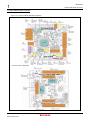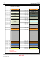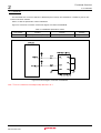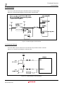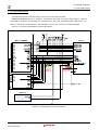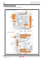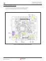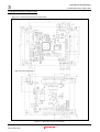
1
REJ10J1564-0104
SH7285 CPU Board
32
M3A-HS85
User's Manual
Renesas 32-Bit RISC Microcomputers
SuperH RISCengine Family / SH7285 Group
TM
Rev. 1.04
Issued: Jul 15, 2008
Notes regarding these materials
1. This document is provided for reference purposes only so that Renesas customers may select the appropriate
Renesas products for their use. Renesas neither makes warranties or representations with respect to the
accuracy or completeness of the information contained in this document nor grants any license to any
intellectual property rights or any other rights of Renesas or any third party with respect to the information in
this document.
2. Renesas shall have no liability for damages or infringement of any intellectual property or other rights arising
out of the use of any information in this document, including, but not limited to, product data, diagrams, charts,
programs, algorithms, and application circuit examples.
3. You should not use the products or the technology described in this document for the purpose of military
applications such as the development of weapons of mass destruction or for the purpose of any other military
use. When exporting the products or technology described herein, you should follow the applicable export
control laws and regulations, and procedures required by such laws and regulations.
4. All information included in this document such as product data, diagrams, charts, programs, algorithms, and
application circuit examples, is current as of the date this document is issued. Such information, however, is
subject to change without any prior notice. Before purchasing or using any Renesas products listed in this
document, please confirm the latest product information with a Renesas sales office. Also, please pay regular
and careful attention to additional and different information to be disclosed by Renesas such as that disclosed
through our website. (http://www.renesas.com )
5. Renesas has used reasonable care in compiling the information included in this document, but Renesas
assumes no liability whatsoever for any damages incurred as a result of errors or omissions in the information
included in this document.
6. When using or otherwise relying on the information in this document, you should evaluate the information in
light of the total system before deciding about the applicability of such information to the intended application.
Renesas makes no representations, warranties or guaranties regarding the suitability of its products for any
particular application and specifically disclaims any liability arising out of the application and use of the
information in this document or Renesas products.
7. With the exception of products specified by Renesas as suitable for automobile applications, Renesas
products are not designed, manufactured or tested for applications or otherwise in systems the failure or
malfunction of which may cause a direct threat to human life or create a risk of human injury or which require
especially high quality and reliability such as safety systems, or equipment or systems for transportation and
traffic, healthcare, combustion control, aerospace and aeronautics, nuclear power, or undersea communication
transmission. If you are considering the use of our products for such purposes, please contact a Renesas
sales office beforehand. Renesas shall have no liability for damages arising out of the uses set forth above.
8. Notwithstanding the preceding paragraph, you should not use Renesas products for the purposes listed below:
(1) artificial life support devices or systems
(2) surgical implantations
(3) healthcare intervention (e.g., excision, administration of medication, etc.)
(4) any other purposes that pose a direct threat to human life
Renesas shall have no liability for damages arising out of the uses set forth in the above and purchasers who
elect to use Renesas products in any of the foregoing applications shall indemnify and hold harmless Renesas
Technology Corp., its affiliated companies and their officers, directors, and employees against any and all
damages arising out of such applications.
9. You should use the products described herein within the range specified by Renesas, especially with respect
to the maximum rating, operating supply voltage range, movement power voltage range, heat radiation
characteristics, installation and other product characteristics. Renesas shall have no liability for malfunctions or
damages arising out of the use of Renesas products beyond such specified ranges.
10. Although Renesas endeavors to improve the quality and reliability of its products, IC products have specific
characteristics such as the occurrence of failure at a certain rate and malfunctions under certain use
conditions. Please be sure to implement safety measures to guard against the possibility of physical injury, and
injury or damage caused by fire in the event of the failure of a Renesas product, such as safety design for
hardware and software including but not limited to redundancy, fire control and malfunction prevention,
appropriate treatment for aging degradation or any other applicable measures. Among others, since the
evaluation of microcomputer software alone is very difficult, please evaluate the safety of the final products or
system manufactured by you.
11. In case Renesas products listed in this document are detached from the products to which the Renesas
products are attached or affixed, the risk of accident such as swallowing by infants and small children is very
high. You should implement safety measures so that Renesas products may not be easily detached from your
products. Renesas shall have no liability for damages arising out of such detachment.
12. This document may not be reproduced or duplicated, in any form, in whole or in part, without prior written
approval from Renesas.
13. Please contact a Renesas sales office if you have any questions regarding the information contained in this
document, Renesas semiconductor products, or if you have any other inquiries.
Table of Contents
Chapter1 Overview .............................................................................................................................. 1-1
1.1 Overview .................................................................................................................................................................... 1-2
1.2 Configuration .............................................................................................................................................................. 1-2
1.3 External Specifications ............................................................................................................................................... 1-3
1.4 External View ............................................................................................................................................................. 1-4
1.5 M3A-HS85 Block Diagram.......................................................................................................................................... 1-5
1.6 M3A-HS85 Board Overview ....................................................................................................................................... 1-6
1.7 M3A-HS85 Memory Mapping ..................................................................................................................................... 1-8
1.8 Absolute Maximum Ratings...................................................................................................................................... 1-11
1.9 Recommended Operating Conditions ...................................................................................................................... 1-11
Chapter2 Functional Overview ............................................................................................................ 2-1
2.1 Functional Overview................................................................................................................................................... 2-2
2.2 CPU............................................................................................................................................................................ 2-3
2.3 Memory ...................................................................................................................................................................... 2-4
2.3.1 SH7285 On-Chip Memory ................................................................................................................................. 2-4
2.3.2 SRAM................................................................................................................................................................ 2-4
2.3.3 SDRAM ............................................................................................................................................................. 2-5
2.3.4 EEPROM........................................................................................................................................................... 2-6
2.4 Serial Port Interface.................................................................................................................................................... 2-7
2.5 I/O Ports ..................................................................................................................................................................... 2-8
2.6 Power Supply Module............................................................................................................................................... 2-11
2.7 USB Interface ........................................................................................................................................................... 2-12
2.8 Clock Module............................................................................................................................................................ 2-13
2.9 Reset Module ........................................................................................................................................................... 2-14
2.10 Interrupt Switches................................................................................................................................................... 2-14
2.11 E10A-USB Interface ............................................................................................................................................... 2-15
Chapter3 Operational Specifications ................................................................................................... 3-1
3.1 M3A-HS85 Connectors Outline .................................................................................................................................. 3-2
3.1.1 H-UDI Connector (J1, J2).................................................................................................................................. 3-3
3.1.2 Serial Port Connector (J3)................................................................................................................................. 3-5
3.1.3 Power Supply Connector (J4) ........................................................................................................................... 3-6
3.1.4 External Power Supply Connector for SH7285 (J5, J6)..................................................................................... 3-7
3.1.5 DC Power Jack (J7) .......................................................................................................................................... 3-8
3.1.6 Extension Connectors (J8-J12) ......................................................................................................................... 3-9
3.1.7 Extension Connector (J13).............................................................................................................................. 3-15
3.1.8 USB Connector (J14) ...................................................................................................................................... 3-16
3.1.9 GND Connector (J15) ..................................................................................................................................... 3-17
3.2 Outline of Switches and LEDs .................................................................................................................................. 3-18
3.2.1 CPU Power Supply Select Jumpers (JP1) ...................................................................................................... 3-19
3.2.2 External Power Supply Select Jumper (JP2, JP3, JP4, JP5) .......................................................................... 3-20
3.2.3 FWE Pin Select Jumper (JP6)......................................................................................................................... 3-21
Rev. 1.04 2008.07.15
REJ10J1564-0104
(i)
3.2.4 Serial Port Select Jumper (JP7, JP8) .............................................................................................................. 3-22
3.2.5 Switch and LED Functions .............................................................................................................................. 3-23
3.2.6 Jumper Switch Setting when Using Development Tool ................................................................................... 3-25
3.3 Board Dimensions of M3A-HS85.............................................................................................................................. 3-26
Appendix.............................................................................................................................................A-1
M3A-HS85 SCHEMATICS
Rev. 1.04 2008.07.15
REJ10J1564-0104
(ii)
Chapter1Overview
Chapter1
Overview
1-1
Overview
1
1.1 Overview
1.1 Overview
The M3A-HS85 is the CPU board designed for users to evaluate the functionality and performance of the SH7285
group of Renesas Technology original microcomputer, as well as develop and evaluate the application software for
this group of microcomputers. The Sh7285’s data bus, address bus and various internal peripheral circuit function
pins are connected to the extension connector of the M3A-HS85, allowing users to evaluate the timing relationship
with peripheral devices using measurement instruments or develop extension boards tailored to suit development
purposes. Furthermore, the E10A-USB or the on-chip emulator made by Renesas Technology can also be connected
to the M3A-HS85.
1.2 Configuration
Figure 1.2.1 shows an example of system configuration using the M3A-HS85.
DC 5V
Power Supply
(1.5A min.)
SH7285 CPU Board
M3A-HS85
*
Serial port
connector
USB
SH7285
H-UDI connector
(14-pin or 36-pin)
Extension
connector
HEW
debugger
High-performance*
E10A-USB*
Embeded Workshop(HEW)
SuperH RISC engine *
C/C++ compiler package
USB
Host
computer *
* : It is necessary to prepare separately for software development.
Figure 1.2.1 Example System Configuration of M3A-HS85
Rev.1.04 2008.07.10
REJ10J1564-0104
1-2
Overview
1
1.3 External Specifications
1.3 External Specifications
Table 1.3.1 lists the external specifications of M3A-HS85.
Table 1.3.1 External Specifications of M3A-HS85
No.
Item
Content
SH7285
1
CPU
z
Input(XIN) Clock: 12.5 MHz
z
CPU Clock: Maximum 100 MHz
z
Bus Clock: Maximum 50 MHz
z
On-chip memory
• Flash Memory: 768 KB
• RAM: 32 KB
z
SRAM: 2-Mbyte (16-bit bus width x 1 pc.) (Not mounted)
*Can be mounted only when SH7285 is used in 3.3V.
2
Memory
z
SDRAM: 16-Mbyte (16-bit bus width x 1 pc.) (Not mounted)
*Can be mounted only when SH7285 is used in 3.3V.
z
EEPROM: 128k-bit (Not mounted)
HN58X24128FPIE x 1 pc. (I2C bus connection)
3
4
5
6
Connector
LED
Switch
Package Dimension
Rev.1.04 2008.07.10
REJ10J1564-0104
z
Extension connector (Bus,I/O,VCC,GND)
z
USB connector (Standard-B receptacle)
z
Serial port connector (D-sub 9-pin)
z
H-UDI connector (14-pin)
z
H-UDI connector (36-pin)
z
POWER LED (1pc.)
z
User LED (6pcs.)
z
Reset switch (1pc.)
z
NMI switch (1pc.)
z
IRQ1 switch (1 pc.)
z
DIP switch for system setting (1pc., 4 poles)
z
DIP switch for user (1pc., 4 poles)
z
Dimensions : 100mm x 100mm
z
Mounting form : 6-layer, double side mounted
z
Board configuration : 1 board
1-3
Overview
1
1.4 External View
1.4 External View
Figure 1.4.1 shows the external view of M3A-HS85.
Figure 1.4.1 External View of M3A-HS85
Rev.1.04 2008.07.10
REJ10J1564-0104
1-4
Overview
1
1.5 M3A-HS85 Block Diagram
1.5 M3A-HS85 Block Diagram
Figure 1.5.1 shows the system block diagram of M3A-HS85.
H-UDI connector
(36-pin)
Serial Port
Connector
H-UDI connector
(14-pin)
USB
Connector
H-UDI
AUD
SCI0
USB
EEPROM
(128 k-bit)
SRAM
2 MB
I2C
SH7285
(100 MHz)
*
16
USBXIN
(48 MHz)
XIN
(12.5 MHz)
16
SDRAM
16 MB
*
16
External bus: Maximum 50 MHz
SH7285 CPU Board
M3A-HS85
16
Extension Connectors
: It is not mounted.
* : It can be mounted only when SH7285 is used in 3.3V.
Figure 1.5.1 System Block Diagram of M3A-HS85
Rev.1.04 2008.07.10
REJ10J1564-0104
1-5
Overview
1
1.6 M3A-HS85 Board Overview
1.6 M3A-HS85 Board Overview
Figure 1.6.1 shows the M3A-HS85 board overview.
<Top view of the component side>
<Top view of the solder side>
Figure 1.6.1 M3A-HS85 Board Overview
Rev.1.04 2008.07.10
REJ10J1564-0104
1-6
Overview
1
1.6 M3A-HS85 Board Overview
Table 1.6.1 lists the main components mounted on the M3A-HS85.
Table 1.6.1 Main Components Mounted in the M3A-HS85
Symbol
Parts Name
Remarks
Recommended components
(Part number and manufacture)
U1
CPU
SH7285 (Renesas)
U2
SRAM
Not mounted
R1LV1616RSA-7S (Renesas)
U3
SDRAM
Not mounted
EDS1216AATA-75E (Elpida)
U4
EEPROM
Not mounted
HN58X24128FPIE (Renesas)
U5
RS-232C driver
SP3232ECA(Sipex)
U6
Reset IC
M51957BFP (Renesas)
X1
Oscillator
SG8002DC_12.5MHz (Epson)
X1
Oscillator socket
R110-83-308(Preci-Dip)
X2
Resonator
Not mounted
X3
Oscillator
SG8002JF_48MHz (Epson)
X4
Resonator
Not mounted
J1
H-UDI connector (36pin)
DX10M-36SE(50) (Hirose)
J2
H-UDI connector (14pin)
7614-6002BL(3M)
J3
Serial port connector
XM2C-0942-132L(Omron)
J4
Power supply connector
S2B-XH-A(JST)
External
J5
J6
power
supply Not mounted
power
supply Not mounted
connector
External
connector
CSTCE-G12M5 (Murata)
CSTCZ48M0X12R (Murata)
A2-2PA-2.54DSA (Hirose)
A2-2PA-2.54DSA (Hirose)
J7
DC power jack
Not mounted
HEC0470-01-630 (HOSIDEN)
J8,J10,J11
Extension connector (20pin)
Not mounted
XG4C-2031 (Omron)
J9,J12
Extension connector (40pin)
Not mounted
XG4C-4031 (Omron)
J13
Extension connector (14pin)
Not mounted
7614-6002 (Sumitomo 3M)
J14
USB connector
UBB-4R-D14T-4D(SN)(LF) (JST)
LED1
Power LED
Blue UB1111C (Stanley)
LED2-7
User LED
Green SML-310MT (Rohm)
SW1
Power switch
MS-12AAH1 (Nihon Kaiheiki)
SW2
Reset switch
SW3
DIP switch for user
4 poles A6S-4104 (Omron)
SW4
DIP switch for system setting
4 poles A6S-4104 (Omron)
SW5
NMI switch
Push switch B3SN-3012 (Omron)
SW6
IRQ1 switch
Push switch B3SN-3012 (Omron)
Push switch
B3SN-3012 (Omron)
Rev.1.04 2008.07.10
REJ10J1564-0104
1-7
Overview
1
1.7 M3A-HS85 Memory Mapping
1.7 M3A-HS85 Memory Mapping
Figure 1.7.1, Figure 1.7.2, and Figure 1.7.3 show the memory mapping examples of SH7285 in the M3A-HS85.
Logical space of the SH7285
MCU mode 3
(Single Chip Mode)
H'0000 0000
On-chip ROM(768KB)
H'000B FFFF
H'000C 0000
M3A-HS85 Memory Mapping
H'0000 0000
H'000B FFFF
H'000C 0000
On-chip ROM(768KB)
Reserved
Reserved
H'801F FFFF
H'8020 0000
H'802F FFFF
H'8030 0000
On-chip flash memory
writing/verify space
H'801F FFFF
H'8020 0000
H'802F FFFF
H'8030 0000
On-chip flash memory
writing/verify space
Reserved
Reserved
H'FFF7
H'FFF8
H'FFF8
H'FFF8
H'FFFB
H'FFFC
H'FFFC
H'FFFD
FFFF
0000
7FFF
8000
FFFF
0000
FFFF
0000
On-chip RAM(32KB)
Reserved
SDRAM mode setting
H'FFF7
H'FFF8
H'FFF8
H'FFF8
H'FFFB
H'FFFC
H'FFFC
H'FFFD
FFFF
0000
7FFF
8000
FFFF
0000
FFFF
0000
On-chip RAM(32KB)
Reserved
SDRAM mode setting
Reserved
Reserved
H'FFFD FFFF
H'FFFE 0000
H'FFFF FFFF
Peripheral I/O
H'FFFD FFFF
H'FFFE 0000
H'FFFF FFFF
Peripheral I/O
Figure 1.7.1 Memory Mapping Example of SH7285 (MCU mode 3)
Rev.1.04 2008.07.10
REJ10J1564-0104
1-8
Overview
1
1.7 M3A-HS85 Memory Mapping
Logical space of the SH7285
MCU mode 0, 1
(On-chip ROM disabled mode)
H'0000 0000
M3A-HS85 Memory Mapping
H'0000 0000
SRAM(2MB) *1 *2 *3
CS0 space
H'03FF
H'0400
H'07FF
H'0800
H'0BFF
H'0C00
H'0FFF
H'1000
H'13FF
H'1400
H'17FF
H'1800
FFFF
0000
FFFF
0000
FFFF
0000
FFFF
0000
FFFF
0000
FFFF
0000
H'1BFF FFFF
H'1C00 0000
CS1 space
CS2 space
CS3 space
CS4 space
CS5 space
CS6 space
CS7 space
H'1FFF FFFF
H'2000 0000
User area *3
H'03FF
H'0400
H'07FF
H'0800
H'0BFF
H'0C00
H'0CFF
H'1000
H'13FF
H'1400
H'17FF
H'1800
H'1BFF
H'1C00
H'1FFF
H'2000
FFFF
0000
FFFF
0000
FFFF
0000
FFFF
0000
FFFF
0000
FFFF
0000
FFFF
0000
FFFF
0000
User area
SRAM(2MB) *1 *2
User area
SDRAM(16MB) *2
User area
User area
User area
SRAM(2MB) *1 *2
User area
User area
Reserved
H'FFF7
H'FFF8
H'FFF8
H'FFF8
H'FFFB
H'FFFC
H'FFFC
H'FFFD
FFFF
0000
7FFF
8000
FFFF
0000
FFFF
0000
On-chip RAM(32KB)
Reserved
SDRAM mode setting
Reserved
H'FFF7
H'FFF8
H'FFF8
H'FFF8
H'FFFB
H'FFFC
H'FFFC
H'FFFD
FFFF
0000
7FFF
8000
FFFF
0000
FFFF
0000
On-chip RAM(32KB)
Reserved
SDRAM mode setting
Reserved
H'FFFD FFFF
H'FFFE 0000
H'FFFF FFFF
[Notes]
Peripheral I/O
Reserved
H'FFFD FFFF
H'FFFE 0000
Peripheral I/O
H'FFFF FFFF
*1:CS space to assign is selected according to software. CS space which can be selected at a
time is only one.
*2:It is initially not mounted.
*3:ROM for program is necessary for CS0 space.
Figure 1.7.2 Example Memory Mapping of SH7285 (MCU mode 0,1)
Rev.1.04 2008.07.10
REJ10J1564-0104
1-9
Overview
1
1.7 M3A-HS85 Memory Mapping
Logical space of the SH7285
MCU mode 2
(On-chip ROM enabled mode)
H'0000
H'000B
H'000C
H'01FF
H'0200
H'03FF
H'0400
0000
FFFF
0000
FFFF
0000
FFFF
0000
H'07FF FFFF
H'0800 0000
H'0BFF
H'0C00
H'0FFF
H'1000
H'13FF
H'1400
H'17FF
H'1800
H'1BFF
H'1C00
H'1FFF
H'2000
FFFF
0000
FFFF
0000
FFFF
0000
FFFF
0000
FFFF
0000
FFFF
0000
On-chip ROM(768KB)
Reserved
CS0 space
CS1 space
CS2 space
CS3 space
CS4 space
CS5 space
CS6 space
CS7 space
M3A-HS85 Memory Mapping
H'0000
H'000B
H'000C
H'01FF
H'0200
H'03FF
H'0400
H'07FF
H'0800
H'0BFF
H'0C00
H'0FFF
H'1000
H'13FF
H'1400
H'17FF
H'1800
H'1BFF
H'1C00
H'1FFF
H'2000
0000
FFFF
0000
FFFF
0000
FFFF
0000
FFFF
0000
FFFF
0000
FFFF
0000
FFFF
0000
FFFF
0000
FFFF
0000
FFFF
0000
On-chip ROM(768KB)
Reserved
SRAM(2MB) *1 *2
User area
User area
SRAM(2MB) *1 *2
User area
SDRAM(16MB) *2
User area
User area
User area
SRAM(2MB) *1 *2
User area
User area
Reserved
H'801F FFFF
H'8020 F000
H'802F FFFF
H'8030 0000
On-chip flash memory
writing/verify space
Reserved
H'801F FFFF
H'8020 F000
H'802F FFFF
H'8030 0000
On-chip flash memory
writing/verify space
Reserved
Reserved
H'FFF7
H'FFF8
H'FFF8
H'FFF8
H'FFFB
H'FFFC
H'FFFC
H'FFFD
FFFF
0000
7FFF
8000
FFFF
0000
FFFF
0000
On-chip RAM(32KB)
Reserved
SDRAM mode setting
H'FFF7
H'FFF8
H'FFF8
H'FFF8
H'FFFB
H'FFFC
H'FFFC
H'FFFD
FFFF
0000
7FFF
8000
FFFF
0000
FFFF
0000
On-chip RAM(32KB)
Reserved
SDRAM mode setting
Reserved
H'FFFD FFFF
H'FFFE 0000
H'FFFF FFFF
[Notes]
Peripheral I/O
Reserved
H'FFFD FFFF
H'FFFE 0000
Peripheral I/O
H'FFFF FFFF
*1:CS space to assign is selected according to software. CS space which can be selected at a
time is only one.
*2:It is initially not mounted.
Figure 1.7.3 Example Memory Mapping of SH7285 (MCU mode 2)
Rev.1.04 2008.07.10
REJ10J1564-0104
1-10
Overview
1
1.8 Absolute Maximum Ratings
1.8 Absolute Maximum Ratings
Table 1.8.1 lists the absolute maximum rating of M3A-HS85.
Table 1.8.1 Absolute Maximum Ratings of M3A-HS85
Symbol
Parameter
Rated Value
5VCC
5V System Power Supply Voltage
-0.3V to 6.0V
Relative to VSS
3VCC
3.3V
-0.3V to 4.6V
Relative to VSS
0°C to 50°C
No dewdrops allowed.
System
Power
Supply
Remarks
Voltage
Topr
Operating Ambient Temperature
Use in corrosive gas environment prohibited.
Tstr
Storage Ambient Temperature
-10°C to 60°C
No dewdrops allowed.
Use in corrosive gas environment prohibited.
Note: The ambient temperature refers to the air temperature in places closest possible to the board.
1.9 Recommended Operating Conditions
Table 1.9.1 lists the recommended operating conditions of M3A-HS85.
Table 1.9.1 Recommended Operating Conditions of M3A-HS85
Symbol
Parameter
Rated Value
Remarks
5VCC
5V System Power Supply Voltage
4.5V to 5.5V
Relative to VSS
3VCC
3V System Power Supply Voltage
3.0V to 3.6V
Relative to VSS
-
Maximum Current Consumption in
Within 1A
the Board
Topr
Operating Ambient Temperature
0°C to 50°C
No dewdrops allowed.
Use in corrosive gas environment prohibited.
Rev.1.04 2008.07.10
REJ10J1564-0104
1-11
Overview
1
1.8 Absolute Maximum Ratings
*This is a blank page*
Rev.1.04 2008.07.10
REJ10J1564-0104
1-12
Chapter2Functional Overview
Chapter2
Functional Overview
2-1
Functional Overview
2
2.1 Functional Overview
2.1 Functional Overview
The M3A-HS85 is the SH7285 CPU board that has the functions listed in Table 2.1.1.
Table 2.1.1 lists the functional modules of M3A-HS85.
Table 2.1.1 Functional Modules of M3A-HS85
Section
2.2
Function
CPU
Content
SH7285
• Input(XIN) Clock: 12.5 MHz
• CPU Clock: Maximum 100 MHz
• Bus Clock: Maximum 50 MHz
• On-Chip Memory
- Flash Memory: 768 kBytes
- RAM: 32 kBytes
2.3
Memory
• SRAM : 2-Mbyte (16-bit bus width x 1pc.) (Not mounted)
*Can be mounted only when SH7285 is used in 3.3V.
• SDRAM : 16-Mbyte(16-bit bus width x 1pc.) (Not mounted)
*Can be mounted only when SH7285 is used in 3.3V.
• EEPROM : 128 kBits (Not mounted)
HN58X24128FPIE x 1 pc. (I2C bus connection)
2.4
Serial Port Interface
Connects SCI0 or SCI3 of SH7285 to the serial port connector
2.5
I/O Ports
Connects to the input/output ports of the SH7285
2.6
Power Supply Module
Controls the system power supply of the M3A-HS85
2.7
USB Interface
Connects USB pin of SH7285 to USB connector
2.8
Clock Module
Controls the system clock
2.9
Reset Module
Controls the device reset mounted on the M3A-HS85
2.10
Interrupt Switches
Connect to the NMI pin, IRQ0 pin and test port
2.11
E10A-USB Interface
SH7285 H-UDI/AUD interface
Operational Specifications
Connectors, Switches and LEDs
-
• SH7285 extension connector
• Switches and LEDs
• H-UDI connector
Detailed in Chapter 3.
Rev.1.04 2008.7.10
REJ10J1564-0104
2-2
Functional Overview
2
2.2 CPU
2.2 CPU
The M3A-HS85 contains the 32-bit RISC microcomputer SH7285 that operates with a maximum 100MHz of CPU
clock frequency. The SH7285 includes 768-Kbyte flash memory, and 32-Kbyte RAM, making it useful in a wide range
of applications from data processing to equipment control.
The M3A-HS85 can be operated with a maximum 100MHz of CPU clock frequency (external bus maximum 50
MHz) using a 12.5 MHz input clock.
Figure 2.2.1 shows the SH7285 block diagram in the M3A-HS85.
SH7285
Clock
EXTAL
XTAL
PA15/CK
Mode
SW
MD1
MD0
FWE/ASEBRKAK/ASEBRK
System
control
RES
NMI
WDTOVF
LED for
user
PE9/TIOC3B/FRAME
PE11/TIOC3D
PE12/TIOC4A
PE13/TIOC4B/MRES
PE14/DACK0/TIOC4C/AH
PE15/DACK1/TIOC4D/IRQOUT
DIP
switch
for user
PE0/TIOC0A/TIOC4AS/DREQ0
PE1/TIOC0B/TIOC4BS/TEND0
PE2/TIOC0C/TIOC4CS/DREQ1
PE3/TIOC0D/TIOC4DS/TEND1
EEPROM
PB2/SCL/POE1/IRQ0
PB3/SDA/POE2/IRQ1
USB
USBXTAL
USBEXTAL
PB9/USPND
VBUS
USD+
USDPB10
Serial
port
PE4/TIOC1A/RXD3
PE5/TIOC1B/TIOC3BS/TXD3
GPIO,
Control
signal,
MTU2/2S,
Interrupt,
etc
H-UDI
PA5/SCK1/SSCK/CS5
PA6/TCLKA/RASL
PA7/TCLKB/SCK3/CASL
PA8/TCLKC/TXD3/RDWR
PA9/TCLKD/RXD3/CKE
PA12/WRH/DQMLU/POE8
PA13/WRL/DQMLL
PA14/RD
PA23/TIC5W/POE0/IRQ1/AH/CKE
PA22/TIC5V/CASU/POE4/IRQ2/CASL
PA21/TIC5U/RASU/POE8/IRQ3/RASL
PB11/RXD2/CS6/CS2/CS0/IRQ0
PB12/TXD2/CS7/CS3/CS1/IRQ1
PD20/IRQ4/TIC5WS/SCK4/POE8
PD21/IRQ5/TIC5VS/TXD4
PD25/TIOC4CS/DREQ1
PD26/TIOC3BS/DACK1
PD27/TIOC4AS/DACK0
PD28/TIOC3DS
PD29/TIOC3BS
PD30/TIOC3CS/IRQOUT
PD31/TIOC3AS/ADTRG
PE4/TIOC1A/RXD3
PE5/TIOC1B/TIOC3BS/TXD3
PE6/TIOC2A/TIOC3DS/SCK3
PE7/TIOC2B/RXD2/BS/UBCTRG
PE8/TIOC3A/SCK2
PE10/TIOC3C/TXD2
PC0/A0/POE0
PC1/A1
PC2/A2
PC3/A3
PC4/A4
PC5/A5
PC6/A6
PC7/A7
PC8/A8
PC9/A9
PC10/A10
PC11/A11
PC12/A12
PC13/A13/IRQ0
PC14/A14/IRQ1
PC15/A15/IRQ2
PB0/A16/IRQ3
PB1/A17/REFOUT/ADTRG/IRQ4
PB6/A18/BACK/POE3/IRQ5/RXD0
PB7/A19/BREQ/POE4/IRQ6/TXD0
PB8/A20/WAIT/POE8/IRQ7/SCK0
Switch by JP7
and JP8
PD0/D0
PD1/D1
PD2/D2/TIC5U
PD3/D3/TIC5V
PD4/D4/TIC5W
PD5/D5/TIC5US
PD6/D6/TIC5VS
PD7/D7/TIC5WS
PD8/D8/TIOC3AS
PD9/D9/TIOC3CS
PD10/D10/TIOC3BS
PD11/D11/TIOC3DS
PD12/D12/TIOC4AS
PD13/D13/TIOC4BS
PD14/D14/TIOC4CS
PD15/D15/TIOC4DS
Address bus
Data bus
Serial port,
Extension connector
(J13)
PA0/RXD0/CS0/TDI
PA1/TXD0/CS1/TDO
PA2/SCK0/SCS/CS2/TCK
PA3/RXD1/SSI/CS3/TMS
PA4/TXD1/SSO/CS4/TRST
ASEMD0
Mode SW FWE/ASEBRKAK/ASEBRK
PD16/IRQ0/CS3/AUDATA0
PD17/IRQ1/POE5/SCK3/CS2/AUDATA1
PD18/IRQ2/POE6/TXD3/CS1/AUDATA2
PD19/IRQ3/POE7/RXD3/CS0/AUDATA3
PD22/IRQ6/TIC5US/RXD4/AUDSYNC
PD24/DREQ0/TIOC4DS/AUDCK
PF0/AN0
PF1/AN1
PF2/AN2
PF3/AN3
PF4/AN4
PF5/AN5
PF6/AN6
PF7/AN7
H-UDI
AUD
A/D
Figure 2.2.1 SH7285 Block Diagram
Rev.1.04 2008.7.10
REJ10J1564-0104
2-3
Functional Overview
2
2.3 Memory
2.3 Memory
2.3.1 SH7285 On-Chip Memory
The SH7285 includes a 768-Kbytes flash memory and 32-Kbytes RAM.
2.3.2 SRAM
Two Mbytes of SRAM can be mounted on the M3A-HS85 (Not mounted). In the M3A-HS85 specification, 3.3V
power is supplied to SRAM so that SH7285 should be used in 3.3V when SRAM is mounted (CPU power supply
switch jumper (JP1) should be set to “2-3”). SRAM is controlled by the bus state controller built into SH7285. The
address spaces of SRAM can be switched to CS0 space, CS2 space, and CS6 space by the pin function controller
setting of SH7285.
Table 2.3.1 lists the SRAM specifications. Figure 2.3.1 shows the block diagram for the connection between
SH7285 and SRAM.
Table 2.3.1 SRAM Specifications
Part Number
Bus size
Capacity
Package
R1LV1616RSA-7S
16 bit
2 Mbytes (16-bit x 1M word x 1 pc.)
48-pin TSOP (20 x 12mm)
R1LV1616RSA-7
16M-bit SRAM
(1M Word ×16bit)
SH7285
PB8/A20 - PC1/A1
PD15/D15 - PD0/D0
20
A19 - A0
16
DQ15 - DQ0
3.3V
PB11/CS0/CS2/CS6
BYTE
CS1
Reset
CS2
PA14/RD
OE
PA8/RDWR
WE
PA12/WRH
UB
PA13/WRL
LB
Figure 2.3.1 Block Diagram for Connection Between SH7285 and SRAM
Rev.1.04 2008.7.10
REJ10J1564-0104
2-4
Functional Overview
2
2.3.3 SDRAM
2.3.3 SDRAM
The M3A-HS85 can mount 16Mbytes of SDRAM (Not mounted). In the M3A-HS85 specification, 3.3V power is
supplied to SDRAM so that SH7285 should be used in 3.3V when SDRAM is mounted (CPU power supply switch
jumper (JP1) should be set to “2-3”). The SDRAM is controlled by the bus state controller built into SH7285.
Table 2.3.2 lists the SDRAM specifications. Figure 2.3.2 shows the block diagram for the connection between
SH7285 and SDRAM.
Table 2.3.2 SDRAM Specifications
Specification
Content
Configuration
2M words x 16 bits x 4 banks (1pc.)
Capacity
16 Mbytes
Access Time
5.4ns
CAS Latency
2 (at 40MHz bus clock)
Refresh Interval
4096 refresh cycle every 64ms
Low Address
A11- A0
Column Address
A8 - A0
Number of Banks
4-bank operation controlled by BA0 and BA1
SDRAM
SH7285
PC14/A14
PC13/A13
PC12/A12-PC1/A1
(8M Word x 16bit)
11
BA1
BA0
BA0
A11-A0
A11
-A
0
PA15/CK
PA9/CKE
CLK
CKE
PB12/CS3
CS#
CS
PA6/RASL
#
A
R
S
RAS
PA7/CASL
CAS
PA8/RDWR
WE#
WE
PA12/DQMLU
DQMU
PA13/DQMLL
PD15/D15-PD0/D0
DQML
16
DQ15-DQ0
Figure 2.3.2 Block Diagram for the Connection Between SH7285 and SDRAM
Rev.1.04 2008.7.10
REJ10J1564-0104
2-5
Functional Overview
2
2.3.4 EEPROM
2.3.4 EEPROM
The M3A-HS85 can mount the 128k-bits of EEPROM (Not mounted). The EEPROM is controlled by the I2C bus
interface included in SH7285.
Table 2.3.3 lists the specification outline of EEPROM.
Figure 2.3.3 shows the connection circuit block diagram of SH7285 and EEPROM.
Table 2.3.3 EEPROM Specification Outline
Part Number
Interface
Capacity
Package
HN58X24128FPIE
2-wire system serial (I2C bus)*
128k bit (16k-word x 8-bit)
8-pin SOP
Figure 2.3.3 Block Diagram of SH7285 and EEPROM
Note*: I2C bus is a trademark of Koninklijke Philips Electronics N. V.
Rev.1.04 2008.7.10
REJ10J1564-0104
2-6
Functional Overview
2
2.4 Serial Port Interface
2.4 Serial Port Interface
SCI channel 0 or SCI channel 3 of SH7285 can be connected with the serial port connector in the M3A-HS85 (SCI
channel 3 is connected to serial port connector (J3) in initial setting.). SCI channel to connect to a serial port
connector is switched by the serial port switch jumper (JP7 and JP8).
SCI channel 0 of SH7285 is connected to an H-UDI connector (14-pin and 36-pin). When SCI channel 0 of SH7285
is used as a serial port connector, note that it should not be double-used on the other connectors.
Figure 2.4.1 shows the block diagram of serial port interface in the M3A-HS85.
RS-232C
driver
SH7285
PE4/RXD3
PA0/RXD0
NC
JP
2
1
3
1
2
3
4
PE5/TXD3
PA1/TXD0
JP
GND
1
3
5
6
2
7
8
NC
9
Serial port
connector
DCD
RxD
TxD
DTR
GND
DSR
RTS
CTS
RI
H-UDI connector
PA0/RXD0/CS0/TDI
PA1/TXD0/CS1/TDO
Extension connector
PE4/RXD3
PE5/TXD3
Figure 2.4.1 Block Diagram of Serial Port Interface
Rev.1.04 2008.7.10
REJ10J1564-0104
2-7
Functional Overview
2
2.5 I/O Ports
2.5 I/O Ports
In the M3A-HS85, all of the SH7285's I/O ports are connected to the extension bus connector.
Some I/O ports are connected to DIP switches and LEDs, and users are free to use these ports.
Figure 2.5.1 shows the block diagram of DIP Switch and LEDs.
Table 2.5.1 lists the functions of the SH7285.
Figure 2.5.1 Block Diagram of DIP Switch and LEDs
Rev.1.04 2008.7.10
REJ10J1564-0104
2-8
Functional Overview
2
2.5 I/O Ports
Table 2.5.1 Functions of I/O Ports
SH7285
No
Pin Name
1
2
6
7
8
9
10
11
12
13
14
15
16
17
18
19
20
21
24
25
26
27
28
29
30
31
32
33
36
37
38
39
40
41
42
43
46
47
48
49
50
51
52
53
57
58
59
60
61
62
63
64
67
68
69
PE14/DACK0/TIOC4C/AH
PE15/DACK1/TIOC4D/IRQOUT
PA23/TIC5W/POE0/IRQ1/AH/CKE
PA22/TIC5V/CASU/POE4/IRQ2/CASL
PA21/TIC5U/RASU/POE8/IRQ3/RASL
PC0/A0/POE0
PC1/A1
PC2/A2
PC3/A3
PC4/A4
PC5/A5
PC6/A6
PC7/A7
PC8/A8
PC9/A9
PC10/A10
PC11/A11
PC12/A12
PC13/A13/IRQ0
PC14/A14/IRQ1
PC15/A15/IRQ2
PB0/A16/IRQ3
PB1/A17/REFOUT/ADTRG/IRQ4
PB2/SCL/POE1/IRQ0
PB3/SDA/POE2/IRQ1
PB6/A18/BACK/POE3/IRQ5/RXD0
PB7/A19/BREQ/POE4/IRQ6/TXD0
PB8/A20/WAIT/POE8/IRQ7/SCK0
PD0/D0
PD1/D1
PD2/D2/TIC5U
PD3/D3/TIC5V
PD4/D4/TIC5W
PD5/D5/TIC5US
PD6/D6/TIC5VS
PD7/D7/TIC5WS
PD8/D8/TIOC3AS
PD9/D9/TIOC3CS
PD10/D10/TIOC3BS
PD11/D11/TIOC3DS
PD12/D12/TIOC4AS
PD13/D13/TIOC4BS
PD14/D14/TIOC4CS
PD15/D15/TIOC4DS
PD16/IRQ0/CS3/AUDATA0
PD17/IRQ1/POE5/SCK3/CS2/AUDATA1
PD18/IRQ2/POE6/TXD3/CS1/AUDATA2
PD19/IRQ3/POE7/RXD3/CS0/AUDATA3
PD20/IRQ4/TIC5WS/SCK4/POE8
PD21/IRQ5/TIC5VS/TXD4
PD22/IRQ6/TIC5US/RXD4/AUDSYNC
PD24/DREQ0/TIOC4DS/AUDCK
PD25/TIOC4CS/DREQ1
PD26/TIOC4BS/DACK1
PD27/TIOC4AS/DACK0
70
PD28/TIOC3DS
Rev.1.04 2008.7.10
REJ10J1564-0104
Extension Connector
J8
J9
J10
J11
Remarks
J12
z
z
z
z
z
LED
LED
IRQ1 SW
z
z
z
z
z
z
z
z
z
z
z
z
z
z
z
z
z
z
z
z
EEPROM
EEPROM
z
z
z
z
z
z
z
z
z
z
z
z
z
z
z
z
z
z
z
z
z
z
z
z
z
z
z
z
z
z
z
z
z
z
z
*
*
*
*
z
z
*
*
z
z
z
z
2-9
Functional Overview
2
2.5 I/O Ports
SH7285
No
Pin Name
71
72
73
76
77
78
79
80
81
82
83
87
93
102
103
104
105
106
107
108
111
112
118
119
120
121
122
123
124
125
131
132
133
134
135
136
137
139
140
141
142
143
PD29/TIOC3BS
PD30/TIOC3CS/IRQOUT
PD31/TIOC3AS/ADTRG
PA15/CK
PA14/RD
PA13/WRL/DQMLL
PA12/WRH/DQMLU/POE8
PA9/TCLKD/RXD3/CKE
PA8/TCLKC/TXD3/RDWR
PA7/TCLKB/SCK3/CASL
PA6/TCLKA/RASL
PB9/USPND
PB10
PE0/TIOC0A/TIOC4AS/DREQ0
PE1/TIOC0B/TIOC4BS/TEND0
PE2/TIOC0C/TIOC4CS/DREQ1
PE3/TIOC0D/TIOC4DS/TEND1
PE4/TIOC1A/RXD3
PE5/TIOC1B/TIOC3BS/TXD3
PE6/TIOC2A/TIOC3DS/SCK3
PB11/RXD2/CS6/CS2/CS0/IRQ0
PB12/TXD2/CS7/CS3/CS1/IRQ1
PF0/AN0
PF1/AN1
PF2/AN2
PF3/AN3
PF4/AN4
PF5/AN5
PF6/AN6
PF7/AN7
PA0/RXD0/CS0/TDI
PA1/TXD0/CS1/TDO
PA2/SCK0/SCS/CS2/TCK
PA3/RXD1/SSI/CS3/TMS
PA4/TXD1/SSO/CS4/TRST
PA5/SCK1/SSCK/CS5
PE7/TIOC2B/RXD2/BS/UBCTRG
PE8/TIOC3A/SCK2
PE10/TIOC3C/TXD2
PE9/TIOC3B/FRAME
PE11/TIOC3D
PE12/TIOC4A
144
PE13/TIOC4B/MRES
Extension Connector
J8
J9
J10
J11
Remarks
J12
z
z
z
z
z
z
z
z
z
z
z
z
z
z
z
z
z
z
z
z
z
z
z
DIP switch for user
DIP switch for user
DIP switch for user
DIP switch for user
z
z
z
z
z
z
z
z
z
Pin for analog input
Pin for analog input
Pin for analog input
Pin for analog input
Pin for analog input
Pin for analog input
Pin for analog input
Pin for analog input
J1,J2,J3,J13
J1,J2,J3,J13
*
*
*
z
z
z
z
z
z
z
LED
LED
LED
z
LED
Note *: Connected only when the 0Ω resistance is mounted.
Rev.1.04 2008.7.10
REJ10J1564-0104
2-10
Functional Overview
2
2.6 Power Supply Module
2.6 Power Supply Module
In M3A-HS85, 5V power is input to the board and 3.3V is generated by using a regulator. The regulator used is
output voltage variable type and given voltage value can be generated by changing the resistance value.
5V power can be supplied from DC stabilized power supply (via power supply connector (J4)) and AC adapter (via
DC power supply jack (J7)).
SH7285 system power supply (VCC) can be switched to 3.3V/5V by setting 3V/5V select jumper (JP1)(Initially it is
set to 5V). When VCC is switched, please note the points shown as follows.
• When 5V is set in the state that SRAM or SDRAM is mounted, the voltage that exceeds the maximum rating is
supplied from the address line, data line, and control line to SDRAM or SRAM, and devices could be destroyed. Thus,
using like this must be avoided.
(3.3V is supplied to 3V system device such as SRAM and SDRAM even when 5V is set.)
By setting jumpers, system power (VSS), A/D power (AVCC), AVREF power, and USB power (DrVCC) of SH7285
can be individually supplied from external power supply.
Figure 2.6.1 shows the block diagram of M3A-HS85 power supply circuit.
Extension connector
AVCC
J8 connector
SH7285
5VCC
AVCC
JP4
AVREF
J8 connector
5VCC
AVREF
J4
Power
connector
DC5V
input
Power switch
JP5
3.3V/5V select
jumper (JP1)
5VCC
1
3
J7
DC power jack
5VCC
5V
3.3V
JP
External
power supply
VCC
2
VCC
JP2
VCC_CPU
DrVCC
(USB power supply)
3VCC
JP3
External
power supply
SRAM
Extension connector
SDRAM
It is not initially mounted.
Mountable only for 3.3V operation
Figure 2.6.1 Block Diagram of Power Supply Circuit
Rev.1.04 2008.7.10
REJ10J1564-0104
2-11
Functional Overview
2
2.7 USB Interface
2.7 USB Interface
The M3A-HS85 contains a USB connector (Standard-B receptacle).
When a cable is connected to USB host/hub in the state that this CPU board is not turned on, the voltage is
impressed from USB host/hub to VBUS. Thus, the CPU board should be turned on before USB cable is connected.
When you want to delay a notification of connection to USB host/hub (the cases such as in the processing of high
priority or initialization), it can be controlled by PB10. The powered state is kept regardless of the states USD+ and
USD- when pin VBUS of SH7285 is set to low level.
Figure 2.7.1 shows the block diagram of M3A-HS85 USB interface.
3.3V
SH7285
DrVCC
PB10
USB
series B
connector
DrVSS
HD74LV1GT08ACME-E
VBUS
Vbus
3.3V
Oscillator (48MHz)
HD74LV1GT126ACME-E
OE
USBEXTAL
USBXTAL
USD+
D+
USD-
DGND
Ceralock
CSTCZ48M0X12R
(Murata)
:Not mounted
Vbus
PB10
VBUS
D+
0
0
0
Hi-Z
0
1
0
Hi-Z
1
0
0
Hi-Z
1
1
1
Pull-up
Remarks
Initial value
When USB is connected
Figure 2.7.1 Block Diagram of USB Interface
Rev.1.04 2008.7.10
REJ10J1564-0104
2-12
Functional Overview
2
2.8 Clock Module
2.8 Clock Module
The clock module in the M3A-HS85 consists of the following two blocks:
•
•
Output from a oscillator connected to EXTAL of the SH7285
Ceramic resonator connected to EXTAL and XTAL
The M3A-HS85 has a 12.5MHz ceramic oscillator connected to it as standard specification. (The oscillator is
mounted via 8-pin IC socket.)
When the ceramic resonator is used, R7 should be removed.
Figure 2.8.1 shows the block diagram of clock module.
Oscillator
SH7285
CLK
EXTAL
*1
R7
0
PA15/CK
Extension connector
XTAL
SDRAM(U3)_CLK pin
Ceramic resonator*1
12.5MHz
*1: To mount the ceramic resonator, R7 should be removed.
: Not mounted component
Figure 2.8.1 Block Diagram of Clock Module
Rev.1.04 2008.7.10
REJ10J1564-0104
2-13
Functional Overview
2
2.9 Reset Module
2.9 Reset Module
This circuit controls the reset signal of SH7285 mounted on the M3A-HS85.
Figure 2.9.1 shows the block diagram of reset module in the M3A-HS85.
Figure 2.9.1 Block Diagram of Reset Module
2.10 Interrupt Switches
In the M3A-HS85, the push switches are connected with the pins NMI and IRQ1 of SH7285.
Figure 2.10.1 shows the block diagram of interrupt switch.
Figure 2.10.1 Block Diagram of Interrupt Switch
Rev.1.04 2008.7.10
REJ10J1564-0104
2-14
Functional Overview
2
2.11 E10A-USB Interface
2.11 E10A-USB Interface
The M3A-HS85 has the H-UDI connectors (J1 and J2) to connect with E10A-USB.
____________________ ________________
ASEBRKAK/ASEBRK/FWE pin of SH7285 is connected to DIP switch for system setting (SW4-1). When the
M3A-HS85 is connected to E10A-USB, SW4-1 should be set to “OFF” after FWE switch jumper (JP6) is set to “1-2”.
When it is connected to E10A-USB in the state that SW4-1 is set to “ON”, it cannot be normally debugged.
Figure 2.11.1 shows the block diagram of E10A-USB interface.
Figure 2.11.1 Block Diagram of E10A-USB Interface
Rev.1.04 2008.7.10
REJ10J1564-0104
2-15
Functional Overview
2
2.11 E10A-USB Interface
*This is a blank page*
Rev.1.04 2008.7.10
REJ10J1564-0104
2-16
Chapter3Operational Specifications
Chapter3
Operational Specifications
3-1
Operational Specifications
3
3.1 M3A-HS85 Connectors Outline
3.1 M3A-HS85 Connectors Outline
Figure 3.1.1 shows the M3A-HS85 connector assignments.
<Top View of the Component Side >
< Top View of the Solder Side >
Figure 3.1.1 M3A-HS85 Connector Assignments
Rev.1.04 2008.7.10
REJ10J1564-0104
3-2
Operational Specifications
3
3.1.1 H-UDI Connector (J1, J2)
3.1.1 H-UDI Connector (J1, J2)
The M3A-HS85 includes a 36-pin H-UDI (J1) connector and 14-pin H-UDI (J2) connector for a connection to the
E10A-USB emulator.
Figure 3.1.2 shows the pin assignments of H-UDI (J1) connector.
35
1
36
2
Top view of the
component side
35
1
Side view
36
2
Board
edge
Board
edge
Figure 3.1.2 Pin Assignments of H-UDI (J1) Connector
Table 3.1.1 lists pin assignments of H-UDI connector (J1).
Table 3.1.1 Pin Assignments of H-UDI (J1) Connector
Pin
Signal Name
Pin
Signal Name
1
AUDCK
19
TMS
2
GND
20
GND
3
AUDATA0
21
GND
22
(GND)
TDI
4
5
_________
TRST
AUDATA1
23
6
GND
24
GND
7
AUDATA2
25
TDO
8
GND
26
GND
9
AUDATA3
27
10
GND
28
GND
AUDSYNC
29
UVCC
GND
11
12
________________
___________________ ______________
ASEBRKAK/ASEBRK
GND
30
13
NC
31
RES
14
GND
32
GND
15
NC
33
GND
16
GND
34
GND
17
TCK
35
NC
18
GND
36
GND
Rev.1.04 2008.7.10
REJ10J1564-0104
_______
3-3
Operational Specifications
3
3.1.1 H-UDI Connector (J1, J2)
Figure 3.1.3 shows the pin assignments of H-UDI (J2) connector.
7
6
5
4
3
2
1
14
13
12
11
10
9
8
Board
edge
Top view of the
component side
J2
Side view
Board
edge
[Note] Please note that the assignments of pin number by Renesas is different
from the assignments of pin number by the manufacturing company of connector.
Figure 3.1.3 Pin Assignments of H-UDI (J2) Connector
Table 3.1.2 lists the pin assignments of H-UDI (J2) connector.
Table 3.1.2 Pin Assignments of H-UDI (J2) Connector
Pin
1
Signal Name
Pin
Signal Name
8
NC
TRST
9
(GND)
TDO
10
GND
ASEBRKAK/ASEBRK
11
UVCC
5
TMS
12
GND
6
TDI
13
GND
14
GND
2
3
4
7
TCK
_________
___________________ ______________
_______
RES
Rev.1.04 2008.7.10
REJ10J1564-0104
3-4
Operational Specifications
3
3.1.2 Serial Port Connector (J3)
3.1.2 Serial Port Connector (J3)
The M3A-HS85 contains a serial port connector (J3).
Figure 3.1.4 shows the pin assignments of serial port connector.
5
9
1
6
Board
edge
Top view of the
component side
1
6
5
9
Board
edge
Side view
Figure 3.1.4 Pin Assignments of Serial Port Connector (J3)
Table 3.1.3 lists the pin assignments of serial port connector.
Table 3.1.3 Pin Assignments of Serial Port Connector (J3)
Pin
Signal Name
Pin
Signal Name
_______
1
NC
6
DSR
2
RXD
7
3
TXD
8
CTS
9
NC
_______
RTS
_______
_______
4
DTR
5
GND
Pins 4-6 and Pins 7-8 are loop back connected.
Rev.1.04 2008.7.10
REJ10J1564-0104
3-5
Operational Specifications
3
3.1.3 Power Supply Connector (J4)
3.1.3 Power Supply Connector (J4)
The M3A-HS85 includes a connector for power supply.
Figure 3.1.5 shows the pin assignments of power supply connector.
1
2
1
2
Top view of the
component side
Board
edge
Side view
Board
edge
Figure 3.1.5 Pin Assignments of Power Supply Connector (J4)
Table 3.1.4 lists the pin assignments of power supply connector for M3A-HS85.
Table 3.1.4 Pin Assignments of Power Supply Connector (J4)
Pin
1
Signal Name
+5V
Rev.1.04 2008.7.10
REJ10J1564-0104
Pin
2
Signal Name
GND
3-6
Operational Specifications
3
3.1.4 External Power Supply Connector for SH7285 (J5, J6)
3.1.4 External Power Supply Connector for SH7285 (J5, J6)
The M3A-HS85 contains a connector pin for external power supply to be supplied to the power for CPU and USB.
When the power is supplied by using this connector, remove the post heads of the external power switch jumpers
(JP2 and JP3) to be in the released state.
Figure 3.1.6 shows the pin assignments of power supply connector.
Top view of the
component side
1 J5 2
1 J6 2
VCC-CPU
DrVCC
Board
edge
Figure 3.1.6 Pin Assignments of Power Supply Connector (J5, J6)
Table 3.1.5 lists the pin assignment of power supply connector (J5) for SH7285.
Table 3.1.5 Pin Assignments of Power Supply Connector for SH7285 (J5)
Pin
1
Signal Name
VCC-CPU
Pin
2
Signal Name
GND
Table 3.1.6 lists the pin assignments of power supply connector (J6) for SH7285.
Table 3.1.6 Pin Assignments of Power Supply Connector for SH7285 (J6)
Pin
1
Signal Name
DrVCC
Rev.1.04 2008.7.10
REJ10J1564-0104
Pin
2
Signal Name
GND
3-7
Operational Specifications
3
3.1.5 DC Power Jack (J7)
3.1.5 DC Power Jack (J7)
A DC power jack can be mounted on the M3A-HS85. Figure 3.1.7 shows the pin assignments of DC power jack,
and Table 3.1.7 lists the pin assignments of DC power jack (J7).
Top view of the
solder side
2
1
J7
3
Board
edge
Figure 3.1.7 Pin Assignments of DC Power Jack (J7)
Table 3.1.7 Pin Assignments of DC Power Jack (J7)
Pin
Signal Name
1
+5V
2
GND
3
GND
Rev.1.04 2008.7.10
REJ10J1564-0104
3-8
Operational Specifications
3
3.1.6 Extension Connectors (J8-J12)
3.1.6 Extension Connectors (J8-J12)
The M3A-HS85 includes the through-hole for mounting extension connectors to which the I/O pins of the SH7285
are connected.
MIL standard connectors can be connected to J8-J12, allowing users to connect with extension boards or monitor
the SH7285 bus signals.
Figure 3.1.8 shows the pin assignments of extension connector.
Board edge
2
40
1
39
19
20
20
2
19
1
J12
J11
Top view of the
solder side
J10
J8
1
2
20
2
19
1
J9
40
2
39
1
Board edge
Board edge
2
40
1
39
J12
2
20
1
19
20
19
J11
Top view of the
component side
J10
J8
J9
2
20
1
19
2
40
1
39
2
1
Board edge
[Note]:The pin numbers on CPU board are defined based on the assumption that extension
connectors are installed in the component side. Thus, the assignments of pin number on the
extension connector side and the CPU board side are different when extension connectors
are installed in the solder side.
Figure 3.1.8 Pin Assignments of Extension Connectors
Rev.1.04 2008.7.10
REJ10J1564-0104
3-9
Operational Specifications
3
3.1.6 Extension Connectors (J8-J12)
Table 3.1.8 lists the pin assignments of extension connector (J8).
Table 3.1.8 Pin Assignments of Extension Connectors (J8)
Pin
Signal Name
Other Connections
1
AVCC
-
2
AVCC
-
3
AVREF
-
4
PF0/AN0
-
5
PF1/AN1
-
6
PF2/AN2
-
7
PF3/AN3
-
8
PF4/AN4
-
9
PF5/AN5
-
10
PF6/AN6
-
11
PF7/AN7
-
12
AVREFVSS
-
13
PE6/TIOC2A/TIOC3DS/SCK3
Extension Connector (J9)
14
AVSS
-
15
AVSS
-
16
NC
-
17
NC
-
18
NC
-
19
NC
-
20
GND
-
Rev.1.04 2008.7.10
REJ10J1564-0104
3-10
Operational Specifications
3
3.1.6 Extension Connectors (J8-J12)
Table 3.1.9 lists the pin assignments of extension connectors (J9).
Table 3.1.9 Pin Assignments of Extension Connectors (J9)
Pin
Signal Name
Other Connections
1
5VCC
-
2
5VCC
-
3
WDTOVF#
-
4
PE6/TIOC2A/TIOC3DS/SCK3
Extension Connector (J8)
5
PE5/TIOC1B/TIOC3BS/TXD3
Serial Port Connector (J3) *When JP7 is ”2-3”
6
PE4/TIOC1A/RXD3
Serial Port Connector (J3) *When JP8 is ”2-3”
7
PE3/TIOC0D/TIOC4DS/TEND1
DIP Switch for User (SW3)
8
PE2/TIOC0C/TIOC4CS/DREQ1
DIP Switch for User (SW3)
9
PB8/A20/WAIT/POE8/IRQ7/SCK0
SRAM (U2) *
10
PB7/A19/BREQ/POE4/IRQ6/TXD0
SRAM (U2) *
11
PB6/A18/BACK/POE3/IRQ5/RXD0
SRAM (U2) *
12
PB1/A17/REFOUT/ADTRG/IRQ4
SRAM (U2) *
13
PB0/A16/IRQ3
SRAM (U2) *
14
PC15/A15/IRQ2
SRAM (U2) *
15
PC14/A14/IRQ1
SRAM (U2) * SDRAM (U3) *
16
PC13/A13/IRQ0
SRAM (U2) * SDRAM (U3) *
17
PC12/A12
SRAM (U2) * SDRAM (U3) *
18
PC11/A11
SRAM (U2) * SDRAM (U3) *
19
PC10/A10
SRAM (U2) * SDRAM (U3) *
20
GND
-
21
PE1/TIOC0B/TIOC4BS/TEND0
DIP Switch for User (SW3)
22
PE0/TIOC0A/TIOC4AS/DREQ0
DIP Switch for User (SW3)
23
PA15/CK
SDRAM (U3) *
24
PC9/A9
SRAM (U2) * SDRAM (U3) *
25
PC8/A8
SRAM (U2) * SDRAM (U3) *
26
PC7/A7
SRAM (U2) * SDRAM (U3) *
27
PC6/A6
SRAM (U2) * SDRAM (U3) *
28
PC5/A5
SRAM (U2) * SDRAM (U3) *
29
PC4/A4
SRAM (U2) * SDRAM (U3) *
30
PC3/A3
SRAM (U2) * SDRAM (U3) *
31
PC2/A2
SRAM (U2) * SDRAM (U3) *
32
PC1/A1
SRAM (U2) * SDRAM (U3) *
33
PC0/A0/POE0
-
34
PB11/RXD2/CS6#/CS2#/CS0#/IRQ0
SRAM (U2) *
35
PA5/SCK1/SSCK/CS5#
-
36
PD20/IRQ4/TIC5WS/SCK4/POE8
-
37
PD21/IRQ5/TIC5VS/TXD4
-
38
PD30/TIOC3CS/IRQOUT
-
39
RESET#
Reset Module
40
GND
-
,
,
,
,
,
,
,
,
,
,
,
,
,
,
Note *: Only when SRAM and SDRAM are mounted.
Rev.1.04 2008.7.10
REJ10J1564-0104
3-11
Operational Specifications
3
3.1.6 Extension Connectors (J8-J12)
Table 3.1.10 lists the pin assignments of extension connectors(J10).
Table 3.1.10 Pin Assignments of Extension Connectors (J10)
Pi
Other Connections
Signal Name
1
PB3/SDA/POE2/IRQ1
EEPROM (U4)
2
PB2/SCL/POE1/IRQ0
EEPROM (U4)
3
PB12/TXD2/CS7#/CS3#/CS1#/IRQ1
SDRAM (U3) *
4
PA8/TCLKC/TXD3/RDWR#
SRAM (U2) *, SDRAM (U3) *
5
PA13/WRL/DQMLL
SRAM (U2) *, SDRAM (U3) *
6
PA12/WRH/DQMLU/POE8
SRAM (U2) *, SDRAM (U3) *
7
PD31/TIOC3AS/ADTRG
-
8
NC (PA4/TXD1/SSO/CS4#/TRST when R93 is mounted)
- (H-UDI connector (J1,J2) when R93 is mounted)
9
PA9/TCLKD/RXD3/CKE
SDRAM (U3) *
10
PA6/TCLKA/RASL#
SDRAM (U3) *
11
PA7/TCLKB/SCK3/CASL#
SDRAM (U3) *
12
NC (PA2/SCK0/SCS/CS2#/TCK when R94 is mounted)
- (H-UDI connector (J1,J2) when R94 is mounted)
13
NC (PA3/RXD1/SSI/CS3#/TMS when R95 is mounted)
- (H-UDI connector (J1,J2) when R95 is mounted)
14
NC (PD16/IRQ0/CS3#/AUDATA0 when R96 is mounted)
- (H-UDI connector (J1) when R96 is mounted)
15
NC
(PD17/IRQ1/POE5/SCK3/CS2#/AUDATA1 when R97 is mounted)
16
NC
(PD18/IRQ2/POE6/TXD3/CS1#/AUDATA2 when R98 is mounted)
17
NC
(PD19/IRQ3/POE7/RXD3/CS0#/AUDATA3 when R99 is mounted)
- (H-UDI connector (J1) when R97 is mounted)
- (H-UDI connector (J1) when R98 is mounted)
- (H-UDI connector (J1) when R99 is mounted)
18
NC (PD22/IRQ6/TIC5US/RXD4/AUDSYNC when R100 is mounted)
- (H-UDI connector (J1) when R100 is mounted)
19
NC (PD24/DREQ0/TIOC4DS/AUDCK when R101 is mounted)
- (H-UDI connector (J1) when R101 is mounted)
20
GND
Note *: Only when SRAM and SDRAM are mounted.
Rev.1.04 2008.7.10
REJ10J1564-0104
3-12
Operational Specifications
3
3.1.6 Extension Connectors (J8-J12)
Table 3.1.11 lists the pin assignments of extension connectors (J11).
Table 3.1.11 Pin Assignments of Extension Connectors (J11)
Pin
Signal Name
Other Connections
1
PD28/TIOC3DS
-
2
PD29/TIOC3BS
-
3
PA14/RD#
SRAM (U2) *, Extension Connector
4
PD15/D15/TIOC4DS
SRAM (U2) *, SDRAM (U3) *, Extension Connector (J12)
5
PD14/D14/TIOC4CS
SRAM (U2) *, SDRAM (U3) *, Extension Connector (J12)
6
PD13/D13/TIOC4BS
SRAM (U2) *, SDRAM (U3) *, Extension Connector (J12)
7
PD12/D12/TIOC4AS
SRAM (U2) *, SDRAM (U3) *, Extension Connector (J12)
8
PD11/D11/TIOC3DS
SRAM (U2) *, SDRAM (U3) *, Extension Connector (J12)
9
PD10/D10/TIOC3BS
SRAM (U2) *, SDRAM (U3) *, Extension Connector (J12)
10
PD9/D9/TIOC3CS
SRAM (U2) *, SDRAM (U3) *, Extension Connector (J12)
(J12)
11
PD8/D8/TIOC3AS
SRAM (U2) *, SDRAM (U3) *, Extension Connector (J12)
12
PD7/D7/TIC5WS
SRAM (U2) *, SDRAM (U3) *, Extension Connector (J12)
13
PD6/D6/TIC5VS
SRAM (U2) *, SDRAM (U3) *, Extension Connector (J12)
14
PD5/D5/TIC5US
SRAM (U2) *, SDRAM (U3) *, Extension Connector (J12)
15
PD4/D4/TIC5W
SRAM (U2) *, SDRAM (U3) *, Extension Connector (J12)
16
PD3/D3/TIC5V
SRAM (U2) *, SDRAM (U3) *, Extension Connector (J12)
17
PD2/D2/TIC5U
SRAM (U2) *, SDRAM (U3) *, Extension Connector (J12)
18
PD1/D1
SRAM (U2) *, SDRAM (U3) *, Extension Connector (J12)
19
PD0/D0
SRAM (U2) *, SDRAM (U3) *, Extension Connector (J12)
20
GND
-
Note *: Only when SRAM and SDRAM are mounted.
Rev.1.04 2008.7.10
REJ10J1564-0104
3-13
Operational Specifications
3
3.1.6 Extension Connectors (J8-J12)
Table 3.1.12 lists the pin assignments of the extension connectors (J12).
Table 3.1.12 Pin Assignments of the Extension Connectors (J12)
Pin
Signal Name
Other Connections
1
3VCC
-
2
3VCC
-
3
PA21/TIC5U/RASU/POE8/IRQ3/RASL
-
4
PA22/TIC5V/CASU/POE4/IRQ2/CASL
-
5
PA23/TIC5W/POE0/IRQ1/AH/CKE
IRQ1 SW (SW6)
6
PB9/USPND
-
7
PB10
USB module
8
PD25/TIOC4CS/DREQ1
-
9
PD26/TIOC4BS/DACK1
-
10
PD27/TIOC4AS/DACK0
-
11
PE7/TIOC2B/RXD2/BS/UBCTRG
-
12
PE8/TIOC3A/SCK2
-
13
PE9/TIOC3B/FRAME
User LED
14
PE10/TIOC3C/TXD2
-
15
PE11/TIOC3D
User LED
16
PE12/TIOC4A
User LED
17
PE13/TIOC4B/MRES#
User LED
18
PE14/DACK0/TIOC4C/AH
User LED
19
PE15/DACK1/TIOC4D/IRQOUT
User LED
20
GND
-
21
NC
-
22
NC
-
23
PA14/RD#
SRAM (U2) *, Extension Connector (J11)
24
PD15/D15/TIOC4DS
SRAM (U2) *, SDRAM (U3) *, Extension Connector (J11)
25
PD14/D14/TIOC4CS
SRAM (U2) *, SDRAM (U3) *, Extension Connector (J11)
26
PD13/D13/TIOC4BS
SRAM (U2) *, SDRAM (U3) *, Extension Connector (J11)
27
PD12/D12/TIOC4AS
SRAM (U2) *, SDRAM (U3) *, Extension Connector (J11)
28
PD11/D11/TIOC3DS
SRAM (U2) *, SDRAM (U3) *, Extension Connector (J11)
29
PD10/D10/TIOC3BS
SRAM (U2) *, SDRAM (U3) *, Extension Connector (J11)
30
PD9/D9/TIOC3CS
SRAM (U2) *, SDRAM (U3) *, Extension Connector (J11)
31
PD8/D8/TIOC3AS
SRAM (U2) *, SDRAM (U3) *, Extension Connector (J11)
32
PD7/D7/TIC5WS
SRAM (U2) *, SDRAM (U3) *, Extension Connector (J11)
33
PD6/D6/TIC5VS
SRAM (U2) *, SDRAM (U3) *, Extension Connector (J11)
34
PD5/D5/TIC5US
SRAM (U2) *, SDRAM (U3) *, Extension Connector (J11)
35
PD4/D4/TIC5W
SRAM (U2) *, SDRAM (U3) *, Extension Connector (J11)
36
PD3/D3/TIC5V
SRAM (U2) *, SDRAM (U3) *, Extension Connector (J11)
37
PD2/D2/TIC5U
SRAM (U2) *, SDRAM (U3) *, Extension Connector (J11)
38
PD1/D1
SRAM (U2) *, SDRAM (U3) *, Extension Connector (J11)
39
PD0/D0
SRAM (U2) *, SDRAM (U3) *, Extension Connector (J11)
40
GND
-
Note *: Only when SRAM and SDRAM are mounted.
Rev.1.04 2008.7.10
REJ10J1564-0104
3-14
Operational Specifications
3
3.1.7 Extension Connector (J13)
3.1.7 Extension Connector (J13)
J13 is the one having installed it for the examination when this board is developed. Please do not use it.
Top view of the
component side
Connector mounting hole
13
11
9
7
5
3
1
14
12
10
8
6
4
2
J13
Board
edge
Figure 3.1.9 Pin Assignments of the Extension Connectors (J13)
Rev.1.04 2008.7.10
REJ10J1564-0104
3-15
Operational Specifications
3
3.1.8 USB Connector (J14)
3.1.8 USB Connector (J14)
The M3A-HS85 has a connector for USB (series B plug).
Figure 3.1.10 shows the pin assignments of USB connector (J14), and Table 3.1.13 lists the pin assignments of
USB connector (J14).
Top view of the
component side
1
4
2
3
Board
edge
Side view
Board
edge
2
1
3
4
Figure 3.1.10 Pin Assignments of USB Connector (J14)
Table 3.1.13 Pin Assignments of USB Connector (J14)
Pin
Signal Name
1
Vbus
2
D-
3
D+
4
GND
Rev.1.04 2008.7.10
REJ10J1564-0104
3-16
Operational Specifications
3
3.1.9 GND Connector (J15)
3.1.9 GND Connector (J15)
The M3A-HS85 has a connector for GND. This is because GND such as measuring instruments can be easily
connected when debugging.
Figure 3.1.11 shows the pin assignments of GND connector (J15). Table 3.1.14 lists the pin assignments of GND
connector (J15).
GND
1
3
Top view of the
component side
J15
Board
edge
Figure 3.1.11 Pin Assignments of GND Connector (J15)
Table 3.1.14 Pin Assignments of GND Connector (J15)
Pin
Signal Name
1
GND
2
GND
3
GND
Rev.1.04 2008.7.10
REJ10J1564-0104
3-17
Operational Specifications
3
3.2 Outline of Switches and LEDs
3.2 Outline of Switches and LEDs
The M3A-HS85 includes switches and LEDs as its operational components.
Figure 3.2.1 shows the M3A-HS85 operational component assignment.
<Top View of the Component Side >
Figure 3.2.1 M3A-H85 Operational Component Assignment
Rev.1.04 2008.7.10
REJ10J1564-0104
3-18
Operational Specifications
3
3.2.1 CPU Power Supply Select Jumpers (JP1)
3.2.1 CPU Power Supply Select Jumpers (JP1)
The power voltage supplied to SH7285 can be switched to 3.3V supply or 5V supply by setting JP1.
The power voltage which can be switched in this jumper is only SH7285 (U1). The supply voltages for the
components such as external memories are not changed.
Figure 3.2.2 shows the pin assignments of select jumper for CPU power supply. Table 3.2.1 lists the pin
assignments of jumper for CPU power supply select jumper for CPU power supply.
Top view of the
component side
1
3.3V 5V
3
JP1 PWRSEL
Board
edge
Board
edge
Figure 3.2.2 Pin Assignments of Select Jumper for CPU Power Supply (JP1)
Table 3.2.1 Pin Assignments of Select Jumper for CPU Power Supply (JP1)
Jumper
Setting
Function
JP1
1-2
5V voltage is supplied to CPU
PWRSEL
2-3
3.3V voltage is supplied to CPU
: Initial Setting
Note: Do not change jumper settings during the operation of M3A-HS85. Ensure to turn off the power for the
M3A-HS85 before changing jumper settings.
Rev.1.04 2008.7.10
REJ10J1564-0104
3-19
Operational Specifications
3
3.2.2 External Power Supply Select Jumper (JP2, JP3, JP4, JP5)
3.2.2 External Power Supply Select Jumper (JP2, JP3, JP4, JP5)
By setting JP2 to JP5, the source of power voltage supplying to A/D reference power supply (AVREF), analog
power supply (AVCC), USB power supply (DrVCC), and system power supply of SH7285 can be switched.
Figure 3.2.3 shows the external power supply select jumper assignments. Table 3.2.2 lists the external power
supply select jumper setting.
Top view of the
component side
CPU-VCC SEL
DrVCC SEL
2
JP3
2
JP2
1
1
FIX INT
FIX INT
2
1
2
JP4
FIX AVREF
1
FIX AVCC
AVCC SEL AVREF SEL
JP5
Figure 3.2.3 External Power Supply Select Jumper Assignments (JP2,JP3,JP4,JP5)
Table 3.2.2 External Power Supply Select Jumper Setting (JP2,JP3,JP4,JP5)
Jumper
Setting
JP2
1-2
CPU-VCC SEL
Open
JP3
1-2
DrVCC SEL
Open
JP4
1-2
AVCCSEL
Open
JP5
1-2
AVREFSEL
Open
Function
SH7285 power supply voltage (VCC) is supplied from J4 or J7
External power supply voltage (supplied from J5 or H13)
SH7285 USB power supply (DrVCC) is supplied from J4 or J7 (via regulator)
External power supply voltage (supplied from J6 or H14)
SH7285 AVCC is connected to 5V fixed power supply voltage.
External power supply voltage (supplied from J8 or H8)
SH7285 AVREF is connected to 5V fixed power supply voltage.
External power supply voltage (supplied from J8 or H9)
: Initial Setting
Note: Do not change jumper settings during the operation of M3A-HS85.
Ensure to turn off the power for the M3A-HS85 before changing jumper settings.
Rev.1.04 2008.7.10
REJ10J1564-0104
3-20
Operational Specifications
3
3.2.3 FWE Pin Select Jumper (JP6)
3.2.3 FWE Pin Select Jumper (JP6)
_____________________ ________________
By setting JP6, pin FWE/ASEBRKAK/ASEBRK of SH7285 can be switched if it is connected to SW4-3 and H-UDI
_____________________
connector, or the extension connector (J13). This jumper should be set only when you want the pin FWE/ASEBRKAK/
________________
ASEBRK to be controlled via the extension (J13).
Figure 3.2.4 shows FWE pin select jumper assignment. Table 3.2.3 lists jumper setting for selecting FWE pin.
Top view of the
component side
Board
edge
INT E8a
1
3
JP6
FWESEL
Board
edge
Figure 3.2.4 FWE Pin Select Jumper (JP6) Assignment
Table 3.2.3 FWE Select Jumper Setting (JP6)
Jumper
Setting
Function
_____________________
JP6
1-2
FWESEL
________________
Pin FWE/ ASEBRKAK / ASEBRK of SH7285 is connected to SW4-3 and the H-UDI
connector (J1 and J2).
_____________________ ________________
2-3
Pin FWE/ASEBRKAK/ASEBRK of SH7285 is connected to the extension connector (J13).
: Initial Setting
Note: Do not change jumper settings during the operation of M3A-HS85.
Ensure to turn off the power for the M3A-HS85 before changing jumper settings.
Rev.1.04 2008.7.10
REJ10J1564-0104
3-21
Operational Specifications
3
3.2.4 Serial Port Select Jumper (JP7, JP8)
3.2.4 Serial Port Select Jumper (JP7, JP8)
SCI channel of SH7285 connecting to the serial port connector (J3) is changed by the setting of JP7 and JP8.
SCIF channel 3 is connected to the serial port connector (J3) as the initial setting. When SCI channel 0 is
connected to the serial port connector (J3), note that H-UDI connectors (J1 and J2) and the extension connector
(J13) cannot be used.
Figure 3.2.5 shows the serial port select jumper assignments. Table 3.2.4 lists the serial port select jumper setting.
Top view of the
component side
1
JP7
3 TXD
SEL
TXD3 TXD0
JP8
1
3 RXD
SEL
RXD3 RXD0
Board
edge
Board
edge
Figure 3.2.5 Serial Port Select Jumper Assignments (JP7, JP8)
Table 3.2.4 Serial Port Select Jumper Setting (JP7, JP8)
Jumper
Setting
Function
JP7
1-2
Pin PE5/TXD3 of SH7285 is connected to the serial port connector (J3).
TXDSEL
2-3
Pin PA1/TXD0 of SH7285 is connected to the serial port connector (J3).
JP8
1-2
Pin PE4/RXD3 of SH7285 is connected to the serial port connector (J3).
RXD SEL
2-3
Pin PA0/RXD0 of SH7285 is connected to the serial port connector (J3).
: Initial Setting
Note: Do not change jumper settings during the operation of M3A-HS85.
Ensure to turn off the power for the M3A-HS85 before changing jumper settings.
Rev.1.04 2008.7.10
REJ10J1564-0104
3-22
Operational Specifications
3
3.2.5 Switch and LED Functions
3.2.5 Switch and LED Functions
The M3A-HS85 includes six switches and seven LEDs.
Table 3.2.5 lists switches mounted on M3A-HS85.
Table 3.2.5 Switches Mounted on M3A-HS85
No.
Function
Remarks
SW1
System power on/off switch
-
SW2
System reset input switch
See section 2.9 for details.
SW3
DIP switch for user (4-pole)
PE0, PE1, PE2, and PE3 are pulled up.
SW3-1 OFF : PE0=”H” ON : PE0=”L”
See section 2.5 on chapter 2 for details.
SW3-2 OFF : PE1=”H” ON : PE1=”L”
SW3-3 OFF : PE2=”H” ON : PE2=”L”
SW3-4 OFF : PE3=”H” ON : PE3=”L”
SW4
System setup DIP switch (4-pole)
See Table 3.2.6 for the functions
SW5
NMI input switch
See section 2.10 for details.
SW6
IRQ1 input switch
See section 2.10 for details.
Table 3.2.6 lists the functions of switch SW4. The operation mode of SH7285 is set by the combination of the pins
FWE, MD0, and MD1. Table 3.2.7 lists the SH7285 operating mode setting.
_______________ ___________________
FWE pin is multiplexed with the ASEBRK/ASEBRKAK signal. When E10A-USB is used, SW4-1(FWE) must be set
to “OFF”.
Table 3.2.6 Functions of Switch SW4
No.
Setting
SW4-1
OFF
FWE="H" (Releasing the writing/erasing protects of on-chip flash memory)
Function
FWE
ON
FWE="L" (Setting the writing erasing protects of on-chip flash memory)
SW4-2
OFF
MD1 pin state "H"
MD1
ON
MD1 pin state "L"
SW4-3
OFF
MD0 pin state "H"
MD0
ON
MD0 pin state "L"
SW4-4
OFF
H1=”H”
It is connected to a test hole (H1). You can use it freely like connecting it to the
TP
ON
H1=”L”
input pin of SH7285 via H1.
Operating mode
setting
(See Table 3.2.7)
: Initial Setting
Rev.1.04 2008.7.10
REJ10J1564-0104
3-23
Operational Specifications
3
3.2.5 Switch and LED Functions
Table 3.2.7 SH7285 Operating Mode Setting
SW4-1
SW4-2
SW4-3
(FWE)
(MD1)
(MD0)
SH7285 Operating Mode
Operating
Mode Name
Mode
MCU extension mode 0
ON
ON
ON
Mode 0
ON
ON
OFF
Mode 1
ON
OFF
ON
Mode 2
MCU extension mode 2 (On-chip ROM enabled)
ON
OFF
OFF
Mode 3
Single chip mode (On-chip ROM enabled)
OFF
ON
ON
Mode 4 *
Boot mode (On-chip ROM enabled)
OFF
ON
OFF
Mode 5 *
User boot mode (On-chip ROM enabled)
OFF
OFF
ON
Mode 6 *
User program mode (On-chip ROM enabled)
OFF
OFF
OFF
Mode 7 *
USB boot mode (On-chip ROM enabled)
(On-chip ROM disabled,CS0 space :16bit bus)
MCU extension mode 1
(On-chip ROM disabled,CS0 space:8bit bus)
: Initial Setting
Note: * It is the programming mode of flash memory.
Table 3.2.8 lists the functions of LEDs mounted on M3A-HS85.
Table 3.2.8 Functions of LEDs mounted on M3A-HS85
No.
Color
LED1
Blue
Power-on LED (LED1 lights when power is supplied)
LED2
Green
Open to user (LED2 lights on when PE9 outputs "L")
LED3
Green
Open to user (LED3 lights on when PE11 outputs "L")
LED4
Green
Open to user (LED4 lights on when PE12 outputs "L")
LED5
Green
Open to user (LED5 lights on when PE13 outputs "L")
LED6
Green
Open to user (LED6 lights on when PE14 outputs "L")
LED7
Green
Open to user (LED7 lights on when PE15 outputs "L")
Rev.1.04 2008.7.10
REJ10J1564-0104
Functions/Remarks
3-24
Operational Specifications
3
3.2.6 Jumper Switch Setting when Using Development Tool
3.2.6 Jumper Switch Setting when Using Development Tool
_____________________ ________________
SH7285’s emulator related signals (FWE/ASEBRKAK/ASEBRK, TDI, and TDO) are multiplexed with on-chip flash
writing control pin. Thus, when development tools such as E10A-USB and Flash Development Toolkit (FDT) are used,
the jumper switch should be set as shown in Table 3.2.9.
Table 3.2.9 Setting when Using Connectors
Tool
Setting
Connector
E10A-USB
H-UDI connector
FDT
Serial port connector
Remarks
JP6
JP7,8
SW4-1
SW4-2,3
“1-2”
“1-2”
OFF
-
-
“2-3”
OFF *1
-
-
“2-3”
OFF *1
OFF
Mode 7
OFF
USB boot mode
(J1 or J2)
(J3)
USB connector
(J14)
Flash
Extension connector
programmer
(J13)
“2-3”
“1-2”
-
-
Note:*1: When JP6 is set to “1-2”, it must be set to “OFF”.
Rev.1.04 2008.7.10
REJ10J1564-0104
3-25
Operational Specifications
3
3.3 Board Dimensions of M3A-HS85
3.3 Board Dimensions of M3A-HS85
Figure 3.3.1 shows board dimensions of M3A-HS85.
<Top View of the Component Side >
< Top View of the Solder Side >
Figure 3.3.1 Board Dimensions of M3A-HS85
Rev.1.04 2008.7.10
REJ10J1564-0104
3-26
Appendix
M3A-HS85 SCHEMATICS
A-1
*This is a blank page*
A-2
1
2
3
4
5
SH7285 CPU Board M3A-HS85 SCHEMATICS
A
A
TITLE
PAGE
B
Note:
1
2
3
4
5
6
INDEX
SH7285
EPROM/SRAM/SDRAM
Serial Interface/USB
H-UDI,Reset,Power
Other Connectors,PUSH_SW,LED
5VCC = Digital 5V
3VCC = 3.3V
VCC = ETC 5V/3.3V
VCC_CPU = CPU 5V/3.3V
AVCC = CPU Analog 5V
DrVCC = USB 3.3V
3VCC_SRAM = SRAM 3.3V
3VCC_SDRAM = SDRAM 3.3V
R
RA
VR
C
CE
CP
C
=
=
=
=
=
=
B
Fixed Resistors
Resister Array
Resistor Potentiometers
Ceramic Caps
Electrolytic Caps
Decoupling Caps
C
:not mounted
D
D
CHANGE
RENESAS SOLUTIONS CORPORATION
DRAWN
SCALE
DATE
Ver. 1.03
1
2
CHECKED
DESIGNED
INDEX
( 1
/ 6
DK30694-C
08-07-14
3
APPROVED
M3A-HS85
4
5
)
5
4
3
2
1
GND-AGND
L1
MD0
L
H
L
H
L
H
L
H
H9
AVREF
JP5
XG8S-0231
1
2 L3
VCC
L330
R3
4.7KΩ
R4
4.7KΩ
CP31
0.1µF
R5
[6] AVREFVSS
ON 8
7
6
5
1
2
3
4
R89
0Ω
A6S-4104
SW-TP
H1
TH10
[6]
[6]
[6]
[6]
[6]
[6]
[6]
[6]
JP6
[5] ASEBRKAK#/ASEBRK#
1
2
3
[5] FWE
XG8S-0331
[12.5MHz:CPU] DIP Type
MD0
MD1
FWE/ASEBRKAK#/ASEBRK#
VCC
X1
4
VCC OUT
3
2
GND OE
1
R6
XOUT
XIN
18Ω
VCC
SG-8002DC_12.5MHz_PCC
[3,5,6] RESET#
R1
4.7KΩ
R7
_0Ω
R8
R9
_0Ω
2
LED
1
_CSTCE12M5V
EEPROM
SW
[12.5MHz:CPU]CERALOCK Type
[48MHz:USB]
X3
CP3
0.1µF
4
VCC OUT
3
2
GND OE
1
R11
[6] NMI
_1MΩ
X2
3
VCC
_1MΩ
R13
1
2
CP11
0.1µF
AVREFVSS
116
AVSS
PF0/AN0
PF1/AN1
PF2/AN2
PF3/AN3
PF4/AN4
PF5/AN5
PF6/AN6
PF7/AN7
128
129
114
MD0
MD1
FWE/ASEBRKAK/ASEBRK
95
97
9
10
11
12
13
14
15
16
17
18
19
20
21
24
25
26
27
28
31
32
33
PD0/D0
PD1/D1
PD2/D2/TIC5U
PD3/D3/TIC5V
PD4/D4/TIC5W
PD5/D5/TIC5US
PD6/D6/TIC5VS
PD7/D7/TIC5WS
PD8/D8/TIOC3AS
PD9/D9/TIOC3CS
PD10/D10/TIOC3BS
PD11/D11/TIOC3DS
PD12/D12/TIOC4AS
PD13/D13/TIOC4BS
PD14/D14/TIOC4CS
PD15/D15/TIOC4DS
36
37
38
39
40
41
42
43
46
47
48
49
50
51
52
53
D0
D1
D2
D3
D4
D5
D6
D7
D8
D9
D10
D11
D12
D13
D14
D15
SH7285
118
119
120
121
122
123
124
125
RES
98
NMI
A[20:0] [3,6]
D
VCC
D[15:0]
XTAL
EXTAL
113
[6] PA23/IRQ1
D0
D1
D2
D3
RA2
4
3
2
1
5
6
7
8
D4
D5
D6
D7
RA3
4
3
2
1
A4.7KΩ
5
6
7
8
D8
D9
D10
D11
RA4
8
7
6
5
A4.7KΩ
1
2
3
4
D12
D13
D14
D15
RA1
8
7
6
5
A4.7KΩ
1
2
3
4
D[15:0] [3,6]
PA14/RD
PA13/WRL/DQMLL
PA12/WRH/DQMLU/POE8
PA8/TCLKC/TXD3/RDWR
PB11/RXD2/CS6/CS2/CS0/IRQ0
77
78
79
81
111
PA15/CK
PA9/TCLKD/RXD3/CKE
PA7/TCLKB/SCK3/CASL
PA6/TCLKA/RASL
PB12/TXD2/CS7/CS3/CS1/IRQ1
76
80
82
83
112
PE4/TIOC1A/RXD3
PE5/TIOC1B/TIOC3BS/TXD3
106
107
ASEMD0
115
ASEMD# [5]
PA0/RXD0/CS0/TDI
PA1/TXD0/CS1/TDO
PA2/SCK0/SCS/CS2/TCK
PA3/RXD1/SSI/CS3/TMS
PA4/TXD1/SSO/CS4/TRST
131
132
133
134
135
PA0/RXD0/TDI [4,5]
PA1/TXD0/TDO [4,5]
PA2/TCK [5,6]
PA3/TMS [5,6]
PA4/TRST# [5,6]
PD16/IRQ0/CS3/AUDATA0
PD17/IRQ1/POE5/SCK3/CS2/AUDATA1
PD18/IRQ2/POE6/TXD3/CS1/AUDATA2
PD19/IRQ3/POE7/RXD3/CS0/AUDATA3
PD22/IRQ6/TIC5US/RXD4/AUDSYNC
PD24/DREQ0/TIOC4DS/AUDCK
57
58
59
60
63
64
PD16/AUDATA0 [5,6]
PD17/AUDATA1 [5,6]
PD18/AUDATA2 [5,6]
PD19/AUDATA3 [5,6]
PD22/AUDSYNC# [5,6]
PD24/AUDCK [5,6]
PD20/IRQ4/TIC5WS/SCK4/POE8
PD21/IRQ5/TIC5VS/TXD4
PD25/TIOC4CS/DREQ1
PD26/TIOC4BS/DACK1
PD27/TIOC4AS/DACK0
PD28/TIOC3DS
PD29/TIOC3BS
PD30/TIOC3CS/IRQOUT
PD31/TIOC3AS/ADTRG
61
62
67
68
69
70
71
72
73
PD20/IRQ4 [6]
PD21/IRQ5 [6]
PD25 [6]
PD26 [6]
PD27 [6]
PD28 [6]
PD29 [6]
PD30/IRQOUT# [6]
PD31 [6]
136
8
7
108
137
139
140
PA5/CS5# [6]
PA21/IRQ3 [6]
PA22/IRQ2 [6]
PE6 [6]
PE7/RXD2 [6]
PE8 [6]
PE10/TXD2 [6]
PA23/TIC5W/POE0/IRQ1/AH/CKE
PE9/TIOC3B/FRAME
PE11/TIOC3D
PE12/TIOC4A
PE13/TIOC4B/MRES
PE14/DACK0/TIOC4C/AH
PE15/DACK1/TIOC4D/IRQOUT
[6]
[6]
[6]
[6]
PE0
PE1
PE2
PE3
102
103
104
105
PE0/TIOC0A/TIOC4AS/DREQ0
PE1/TIOC0B/TIOC4BS/TEND0
PE2/TIOC0C/TIOC4CS/DREQ1
PE3/TIOC0D/TIOC4DS/TEND1
[3,6] PB2/SCL
[3,6] PB3/SDA
29
30
PB2/SCL/POE1/IRQ0
PB3/SDA/POE2/IRQ1
USB_XOUT
85
USBXTAL
USB_XIN
C
A4.7KΩ
WDTOVF
141
142
143
144
1
2
86
USBEXTAL
[6] PB9/USPND
87
PB9/USPND
[4] VBUS
88
VBUS
[4] DP
[4] DM
90
91
USD+
USD-
[4,6] PB10
93
PB10
89
DrVCC
92
DrVSS
_0Ω
0.1µF
CP12
0.1µF
CP33
CP4
0.1µF
_CSTCE48M0X11R
+
CP10
0.1µF
AVREF
127
6
Decoupling Caps
CP9
0.1µF
AVCC
126
130
CP5
0.1µF
CP8
0.1µF
117
PC0/A0/POE0
PC1/A1
PC2/A2
PC3/A3
PC4/A4
PC5/A5
PC6/A6
PC7/A7
PC8/A8
PC9/A9
PC10/A10
PC11/A11
PC12/A12
PC13/A13/IRQ0
PC14/A14/IRQ1
PC15/A15/IRQ2
PB0/A16/IRQ3
PB1/A17/REFOUT/ADTRG/IRQ4
PB6/A18/BACK/POE3/IRQ5/RXD0
PB7/A19/BREQ/POE4/IRQ6/TXD0
PB8/A20/WAIT/POE8/IRQ7/SCK0
A0
A1
A2
A3
A4
A5
A6
A7
A8
A9
A10
A11
A12
A13
A14
A15
A16
A17
A18
A19
A20
PA14/RD# [3,6]
PA13/WRL#/DQMLL [3,6]
PA12/WRH#/DQMLU [3,6]
PA8/RD/WR# [3,6]
PB11/CS0#/CS2#/CS6# [3,6]
CLKOUT
R10
22Ω
PA15/CK [3,6]
PA9/CKE [3,6]
PA7/CASL# [3,6]
PA6/RASL# [3,6]
PB12/CS7#/CS3#/CS1#
PE4/RXD3 [4,6]
PE5/TXD3 [4,6]
[3,6]
B
DrVCC
X4
3
VCC_CPU
VCC
VCC
VCC
VCC
VCC
VCC
VCC
VCC
VCC
PE9/TIOC3B
PE11/TIOC3D
PE12/TIOC4A
PE13/TIOC4B
PE14/TIOC4C
PE15/TIOC4D
USB
R12
3
22
34
44
55
65
74
96
109
[6] WDTOVF#
0Ω
R110
_0Ω
A[20:0]
[6]
[6]
[6]
[6]
[6]
[6]
SG-8002JF_48MHz_PCC
B
0Ω
PF0/AN0
PF1/AN1
PF2/AN2
PF3/AN3
PF4/AN4
PF5/AN5
PF6/AN6
PF7/AN7
[5] MD0
[5] MD1
0.1µF
AVREF
[6] AVREF
SW4
C
CP1
0.1µF
+
SH7285_144
U1
VCC_CPU
L330
CE11
10µF/16V
R2
4.7KΩ
CP2
AVCC
Serial
(COM)
MD1
L
L
H
H
L
L
H
H
FWE
L
L
L
L
H
H
H
H
JP4
XG8S-0231
1
2 L2
H-UDI
MODE
0
1
2
3
4
5
6
7
H8
AVCC
5VCC
AUD
D
Mode Switch
Test Pin Switch
L330
CP13
0.1µF
CP14
0.1µF
CP15
0.1µF
CP16
0.1µF
CE12
4.7µF
CP6
0.1µF
CP7
0.1µF
4
54
101
VCL
VCL
VCL
100
PLLVSS
5
23
35
45
56
66
75
84
94
99
110
138
VSS
VSS
VSS
VSS
VSS
VSS
VSS
VSS
VSS
VSS
VSS
VSS
PA5/SCK1/SSCK/CS5
PA21/TIC5U/RASU/POE8/IRQ3/RASL
PA22/TIC5V/CASU/POE4/IRQ2/CASL
PE6/TIOC2A/TIOC3DS/SCK3
PE7/TIOC2B/RXD2/BS/UBCTRG
PE8/TIOC3A/SCK2
PE10/TIOC3C/TXD2
A
A
CHANGE
RENESAS SOLUTIONS CORPORATION
DRAWN
CHECKED
DESIGNED
APPROVED
M3A-HS85
CPU_SH7285
( 2
SCALE
Ver. 1.03
As for CP33, even not mounting is possible.
5
4
DATE
DK30694-C
08-07-14
3
2
1
/ 6
)
1
2
4
SRAM CS2
16bit access = 2MByte
SRAM
A
3
SDRAM
5
SDRAM
16bit access = 16MB
A
D[15:0]
[2,6] D[15:0]
A[20:0]
[2,6] A[20:0]
U3
R14
4.7KΩ
R15
4.7KΩ
BYTE#
WE#
UB#
LB#
CS1#
CS2#
OE#
B
[2,6] PB11/CS0#/CS2#/CS6#
[2,5,6] RESET#
[2,6] PA14/RD#
A19
A18
A17
A16
A15
A14
A13
A12
A11
A10
A9
A8
A7
A6
A5
A4
A3
A2
A1
A0
47
11
14
15
26
12
28
BYTE#
WE#
UB#
LB#
CS1#
CS2#
OE#
DQ15/A-1
DQ14
DQ13
DQ12
DQ11
DQ10
DQ9
DQ8
DQ7
DQ6
DQ5
DQ4
DQ3
DQ2
DQ1
DQ0
D15
D14
D13
D12
D11
D10
D9
D8
D7
D6
D5
D4
D3
D2
D1
D0
45
43
41
39
36
34
32
30
44
42
40
38
35
33
31
29
NC
NC
10
13
VCC
37
R17
0Ω
R18
0Ω
1
2
8 A22Ω
7 A22Ω
SA14
SA13
21
20
BA1
BA0
A12
A11
A10
A9
A8
RA5C
RA5D
RA7A
RA7B
RA7C
3
4
1
2
3
6
5
8
7
6
A22Ω
A22Ω
A22Ω
A22Ω
A22Ω
SA12
SA11
SA10
SA9
SA8
35
22
34
33
32
A11
A10
A9
A8
A7
A7
A6
A5
A4
A3
A2
A1
RA7D
RA9A
RA9B
RA9C
RA9D
RA10A
RA10B
4
1
2
3
4
1
2
5
8
7
6
5
8
7
A22Ω
A22Ω
A22Ω
A22Ω
A22Ω
A22Ω
A22Ω
SA7
SA6
SA5
SA4
SA3
SA2
SA1
31
30
29
26
25
24
23
A6
A5
A4
A3
A2
A1
A0
36
40
NC
NC
19
18
17
16
CS
RAS
CAS
WE
39
15
DQMU
DQML
37
38
CKE
CLK
VCC
R92
4.7KΩ
[2,6] PB12/CS7#/CS3#/CS1#
[2,6] PA6/RASL#
[2,6] PA7/CASL#
46
27
_R1LV1616RSA-7SR
R16
_0Ω
RA5A
RA5B
3VCC_SRAM
CP17
0.1µF
VSS
VSS
A14
A13
[2,6] PA9/CKE
[2,6] PA15/CK
R19
0Ω
RA6
EDS1216AATA
VCC
9
16
17
48
1
2
3
4
5
6
7
8
18
19
20
21
22
23
24
25
R1LV1616RSA-7SR
U2
A20
A19
A18
A17
A16
A15
A14
A13
A12
A11
A10
A9
A8
A7
A6
A5
A4
A3
A2
A1
[2,6] PA8/RD/WR#
[2,6] PA12/WRH#/DQMLU
[2,6] PA13/WRL#/DQMLL
SRAM
R16
R17
R18
R19
not mounted
mounted
mounted
mounted
DQ15
DQ14
DQ13
DQ12
53
51
50
48
SD15
SD14
SD13
SD12
DQ11
DQ10
DQ9
DQ8
47
45
44
42
SD11
SD10
SD9
SD8
DQ7
DQ6
DQ5
DQ4
13
11
10
8
SD7
SD6
SD5
SD4
DQ3
DQ2
DQ1
DQ0
7
5
4
2
SD3
SD2
SD1
SD0
VDD
VDD
VDD
1
14
27
VSS
VSS
VSS
54
41
28
3VCC_SDRAM
VDDQ
VDDQ
VDDQ
VDDQ
3
9
43
49
CP21
0.1µF
VSSQ
VSSQ
VSSQ
VSSQ
52
46
12
6
RA8
5
6
7
8
5
6
7
8
RA11
1
2
3
4
RA12
1
2
3
4
A0Ω
4
3
2
1
A0Ω
4
3
2
1
A0Ω
8
7
6
5
A0Ω
8
7
6
5
D15
D14
D13
D12
D11
D10
D9
D8
D7
D6
D5
D4
D3
D2
D1
D0
3VCC_SDRAM
CP18
0.1µF
CP19
0.1µF
CP20
0.1µF
CP22
0.1µF
CP23
0.1µF
B
CP24
0.1µF
_EDS1216AATA-75-E
FLASH ROM
mounted
not mounted
not mounted
not mounted
3VCC
3VCC
3VCC_SRAM
L4
3VCC_SDRAM
H10
L330
H11
L5
L330
3V_SRAM
3V_SDRAM
VCC
C
R20
4.7KΩ
CP25
0.1µF
R21
4.7KΩ
C
U4
R23
R22
[2,6] PB2/SCL
[2,6] PB3/SDA
VCC
8
7
6
5
0Ω
0Ω
VCC
WP
SCL
SDA
A0
A1
A2
VSS
1
2
3
4
_HN58X24128FPIE
D
D
CHANGE
RENESAS SOLUTIONS CORPORATION
DRAWN
CHECKED
DESIGNED
APPROVED
M3A-HS85
EEPROM/SRAM/SDRAM
( 3
/ 6
SCALE
Ver. 1.03
The unmounting mark is added to the product number of SRAM, SDRAM, and EEPROM
1
2
DATE
08-07-14
3
4
DK30694-C
5
)
5
4
3
2
1
D
D
USB Connector
R28
[2,6] PB10
H12
VBUS
10KΩ
U7A
1
2
4
[2] VBUS
0V - 3.3V
R24
HD74LV1GT08ACME-E
3VCC
U8
3VCC
R25
1
2
3
1KΩ
OE
A
GND
VCC
5
Y
4
CP26
0.1µF
C14
0.1µF
L6
10KΩ
_L600
R29
20KΩ
C1
1µF
USB B
J14
HD74LV1GT126ACME-E
4
USB-DM
USB-DP
<-- Same voltage as VCC_CPU
U7B
3
CP32
0.1µF
2
1
2
3
4
Vbus
DD+
GND
5
6
7
8
FRAME
FRAME2
FRAME3
FRAME4
UBB-4R-D14T-4D(LF)(SN)
D1
C
4
VCC
5
C
5
1
24Ω
2
R27
[2] DP
VBUS-IN
L7
_DLW21HN900SQ2
1
R111
1.5KΩ
_HZM6.2Z4MFA
3
[2] DM
24Ω
3
R26
HD74LV1GT08ACME-E
L8
_L600
Serial Port Connector(COM)
[2,6] PE5/TXD3
1
2
3
[2,5] PA1/TXD0/TDO
XG8S-0331
VCC
TxD_A
R30
0Ω
TxD_B
RxD_A
R31
0Ω
RxD_B
5
C2-
12
11
10
9
R32
0Ω
R1OUT
T1IN
T2IN
R2OUT
VCC
C1C2+
2
V-
6
UART connector
mount hole = GND
C5
0.1µF
R1IN
T1OUT
T2OUT
R2IN
B
C3
0.1µF
13
14
7
8
RI#
DTR#
CTS#
TxD
RTS#
RxD
DSR#
DCD#
TxD
RxD
SP3232ECA-L
J3
5
9
4
8
3
7
2
6
1
VCC
10
C4
0.1µF
JP7
3
4
V+
11
R34
4.7KΩ
C1+
15
C2
0.1µF
B
1
GND
U5
VCC
16
VCC
XM2C-0912-112
R33
4.7KΩ
+
CP27
0.1µF
JP8
[2,6] PE4/RXD3
CE1
4.7µF
Decoupling Caps
for SP3232E
1
2
3
[2,5] PA0/RXD0/TDI
XG8S-0331
A
A
CHANGE
RENESAS SOLUTIONS CORPORATION
DRAWN
CHECKED
DESIGNED
APPROVED
M3A-HS85
USB/SERIAL Interface
( 4
/ 6
SCALE
Ver. 1.03
DATE
USB surroundings, IC, and connected power supply change
5
4
08-07-14
3
2
DK30694-C
1
)
1
2
3
4
5
H-UDI Interface
5V To 3.3V Linear Regulator
VCC
VCC
RA14
A4.7KΩ
Power
Switch
29
[2,6]
[2,6]
[2,6]
[2,6]
[2,6]
PD24/AUDCK
PD16/AUDATA0
PD17/AUDATA1
PD18/AUDATA2
PD19/AUDATA3
[2,6] PD22/AUDSYNC#
R41
R38
R42
R39
R43
0Ω
0Ω
0Ω
0Ω
0Ω
AUDCK
AUDATA0
AUDATA1
AUDATA2
AUDATA3
1
3
5
7
9
R40
0Ω
AUDSYNC
11
17
19
21
23
25
27
31
[2,6] PA2/TCK
[2,6] PA3/TMS
[2,6] PA4/TRST#
[2,4] PA0/RXD0/TDI
[2,4] PA1/TXD0/TDO
[2] ASEBRKAK#/ASEBRK#
37
38
Power LED
A
5VCC
H-UDI (36PIN)
J1
1
2
3
4
1
2
3
4
VCC
NC
NC
NC
15
13
35
GND
GND
GND
GND
_AUDSYNC GND
GND
TCK
GND
TMS
GND
_TRST
GND
TDI
GND
TDO
ASEMD
_ASEBRAK GND
_RES
GND
GND
GND
GND
GND
FRAME
GND
FRAME
GND
2
4
6
8
10
12
14
16
18
20
22
24
26
28
30
32
33
34
36
UVCC
AUDCK
AUDATA0
AUDATA1
AUDATA2
AUDATA3
J4
S2B-XH-A
1
2
3VCC
U9
LMS1587CS-ADJ
SW1
VCC_IN
1
2
VCC
3
VIN
3
MS-12AAH1
+ CE2
10µF/16V
Power
Connector
R46
4.7KΩ
5VCC
VOUT
2
TAB
4
R45
1KΩ
R44
110Ω
A
A
+ CE3
22µF
+ CE4
22µF
LED1
UB1111C
BLUE
K
R37
4.7KΩ
ADJ
R36
4.7KΩ
1
RA13
A4.7KΩ
8
7
6
5
R35
4.7KΩ
8
7
6
5
1-2 Power On
2-3 Power Off
R48
4.7KΩ
R47
180Ω
J7
1
2
3
ASEMD# [2]
HEC0470-01-630
VCC_CPU EXTERNAL
DX10M-36SE
3VCC
VCC
11
1
2
3
4
5
6
7
B
5VCC
UVCC
NC
TCK
_TRST
ASEMD
TDO
GND
_ASEBRAK GND
TMS
GND
TDI
GND
_RES
VCC
8
JP2
1
1
2
3
1-2 5V
2-3 3.3V
VCC_CPU
1
2
XG8S-0231
XG8S-0331
9
10
12
13
14
[2] FWE
[2] MD0
[2] MD1
R49
1KΩ
RES#
+ CE5
10µF/16V
+
_A2-2PA-2.54DSA
CE6
10µF/16V
B
DrVCC EXTERNAL
DrVCC
H14
J6
2
XG8S-0231
J13
VCC_CPU
DrVCC
JP3
1
1
2
3
4
5
6
7
8
9
10
11
12
13
14
J5
2
7614-6002
VCC
VCC_CPU
H13
JP1
H-UDI (14PIN)
J2
E8a
NC
NC
IO1
IO2
RECEIVE
IO3
NC
UVCC
NC
NC
SEND
NC
RES
UCON
1
2
DrVCC
+ CE7
10µF/16V
+
_A2-2PA-2.54DSA
CE8
10µF/16V
POWER TEST PIN
5VCC
7614-6002
VCC
3VCC
H15
H17
H19
5V
VCC
3VCC
H16
H18
H20
5V
VCC
3VCC
C
C
Power On Reset
Board fixed hole.
MH1
1
VCC
1
HOLE
H21
MH2
1
J15
R51
10KΩ
R50
4.7KΩ
8
OUT
Cd
6
R52
0Ω
5
R53
100Ω
1
1
3
MH3
1
2
RESET# [2,3,6]
XG8S-0331
GND
HD74LV2G14A
H23
MH4
1
VCC
CP28
0.1µF
3
4
CP29
0.1µF
H24
U10C
U10D
HD74LV2G14A
1
HOLE
GND
B3SN-3012
1
HOLE
SW2
4
3
M51957BFP
H22
U10B
6
8
4
R54
10KΩ
7
HD74LV2G14A
2
1
IN
U10A
GND
VCC
NC
NC NC
2
7
U6
1
HOLE
1
2
3
GND
5
GND
HD74LV2G14A
D
D
CHANGE
RENESAS SOLUTIONS CORPORATION
DRAWN
CHECKED
DESIGNED
APPROVED
M3A-HS85
H-UDI,Power,Reset
( 5
/ 6
SCALE
DATE
Ver. 1.03
1
2
08-07-14
3
4
DK30694-C
5
)
5
4
3
2
1
5VCC
LED&SW
SH7285 Extension
Connector
R55
VCC
A
A
[2] WDTOVF#
GREEN
LED2
SML-310MT
GREEN
LED3
SML-310MT
GREEN
LED4
SML-310MT
[2,4] PE5/TXD3
[2,4] PE4/RXD3
K
PE11
PE12
H2
H3
H4
TH10 TH10 TH10
R64
R61
R60
[2] PE9/TIOC3B
[2] PE11/TIOC3D
[2] PE12/TIOC4A
0Ω
0Ω
0Ω
J9
K
PE9
LED2
LED3
LED4
PE3
PE2
PE1
PE0
AVCC
R90
R91
VCC
0Ω
A/D Connector
A
A
A
GREEN
LED5
SML-310MT
GREEN
LED6
SML-310MT
GREEN
LED7
SML-310MT
K
K
PE14
PE15
H5
H6
H7
TH10 TH10 TH10
R66
R68
R67
[2] PE13/TIOC4B
[2] PE14/TIOC4C
[2] PE15/TIOC4D
0Ω
0Ω
0Ω
R65
330Ω
K
PE13
R63
330Ω
[2]
[2]
[2]
[2]
[2]
[2]
[2]
[2]
[2]
[2]
[2]
LED5
LED6
LED7
AVREF
PF0/AN0
PF1/AN1
PF2/AN2
PF3/AN3
PF4/AN4
PF5/AN5
PF6/AN6
PF7/AN7
AVREFVSS
PE6
R102
R103
R104
R105
R106
R107
R108
R109
0Ω
0Ω
0Ω
0Ω
0Ω
0Ω
0Ω
0Ω
_0.1µFx8
VCC
AGND
C
R69
4.7KΩ
[2]
[2]
[2]
[2]
R74
R73
R76
R75
PE0
PE1
PE2
PE3
R70
4.7KΩ
R71
4.7KΩ
R72
4.7KΩ
AGND
SW8_1
SW8_2
SW8_3
SW8_4
8 ON
7
6
5
1
2
3
4
[2,3]
[2,3]
[2]
[2]
[2]
[2]
[2,3,5]
A6S-4104
NMI SWITCH CIRCUIT
U11B
4
0Ω
_XG4C-4031
2
A[20:0]
PB11/CS0#/CS2#/CS6#
PA5/CS5#
PD20/IRQ4
PD21/IRQ5
PD30/IRQOUT#
RESET#
3VCC
R77
0Ω
VCC
NMI_SW
U11A
3
1
SN74LVC14APW
+
SN74LVC14APW
R80
10KΩ
R81
220Ω
CE9
SW5
NMI
SWITCH
[2]
[2]
[2]
[2]
[2,4]
[2]
[2]
[2]
[2]
[2]
B3SN-3012
IRQ SWITCH CIRCUIT
B
0Ω
10
11
VCC
IRQ_SW
U11F
12
13
R82
10KΩ
R84
220Ω
PA21/IRQ3
PA22/IRQ2
PA23/IRQ1
PB9/USPND
PB10
PD25
PD26
PD27
PE7/RXD2
PE8
[2] PE10/TXD2
4
3
[2] PA23/IRQ1
U11E
SN74LVC14APW
+
SN74LVC14APW
CE10
SW6
IRQ1
SWITCH
B3SN-3012
2
1
2.2µF
U11D
8
U11C
9
6
SN74LVC14APW
5
SN74LVC14APW
14
VCC
VCC
VSS
7
CP30
0.1µF
R78
0Ω
J12
2
1
2.2µF
R83
C
_XG4C-2031
C7 C9 C11 C13
C6 C8 C10 C12
1
2
3
4
5
6
7
8
9
10
11
12
13
14
15
16
17
18
19
20
21
22
23
24
25
26
27
28
29
30
31
32
33
34
35
36
37
38
39
40
4
3
[2] NMI
PE1
PE0
PA15/CK
A9
A8
A7
A6
A5
A4
A3
A2
A1
A0
1
2
3
4
5
6
7
8
9
10
11
12
13
14
15
16
17
18
19
20
D
SW3
0Ω
0Ω
0Ω
0Ω
R79
J8
0Ω
1
2
3
4
5
6
7
8
9
10
11
12
13
14
15
16
17
18
19
20
21
22
23
24
25
26
27
28
29
30
31
32
33
34
35
36
37
38
39
40
WDTOVF#
PE6
PE5/TXD3
PE4/RXD3
PE3
PE2
A20
A19
A18
A17
A16
A15
A14
A13
A12
A11
A10
PE6
[2,3] PA15/CK
R62
330Ω
0Ω
R59
330Ω
A
D
R58
330Ω
0Ω
K
R57
330Ω
R56
U11G
[2,3]
[2,3]
[2,3]
[2,3]
[2,3]
[2,3]
[2]
[2,5]
[2,3]
[2,3]
[2,3]
[2,5]
[2,5]
[2,5]
[2,5]
[2,5]
[2,5]
[2,5]
[2,5]
PB3/SDA
PB2/SCL
PB12/CS7#/CS3#/CS1#
PA8/RD/WR#
PA13/WRL#/DQMLL
PA12/WRH#/DQMLU
PD31
PA4/TRST#
PA9/CKE
PA6/RASL#
PA7/CASL#
PA2/TCK
PA3/TMS
PD16/AUDATA0
PD17/AUDATA1
PD18/AUDATA2
PD19/AUDATA3
PD22/AUDSYNC#
PD24/AUDCK
R86
R85
J10
0Ω
0Ω
R93
_0Ω
R94
R95
R96
R97
R98
R99
R100
R101
_0Ω
_0Ω
_0Ω
_0Ω
_0Ω
_0Ω
_0Ω
_0Ω
1
2
3
4
5
6
7
8
9
10
11
12
13
14
15
16
17
18
19
20
[2] PD28
[2] PD29
[2,3] PA14/RD#
R88
R87
J11
0Ω
0Ω
PA14/RD#
D15
D14
D13
D12
D11
D10
D9
D8
D7
D6
D5
D4
D3
D2
D1
D0
_XG4C-2031
SN74LVC14APW
1
2
3
4
5
6
7
8
9
10
11
12
13
14
15
16
17
18
19
20
PE9/TIOC3B
PE11/TIOC3D
PE12/TIOC4A
PE13/TIOC4B
PE14/TIOC4C
PE15/TIOC4D
PA14/RD#
D15
D14
D13
D12
D11
D10
D9
D8
D7
D6
D5
D4
D3
D2
D1
D0
_XG4C-2031
B
_XG4C-4031
[2,3] D[15:0]
Decoupling Caps
A
A
CHANGE
RENESAS SOLUTIONS CORPORATION
DRAWN
CHECKED
DESIGNED
APPROVED
M3A-HS85
Connectors
( 6
/ 6
SCALE
DATE
Ver. 1.03
5
4
DK30694-C
08-07-14
3
2
1
)
*This is a blank page*
Revision History
Rev.
SH7285 CPU Board M3A-HS85 User's Manual
Date of Issue
Content of Revision
Page
Point
1.00
08/02/29
-
First edition issued
1.01
08/04/10
-
Second edition issued
1.02
08/05/22
-
Third edition issued
1.03
08/05/27
-
Fourth edition issued
1.04
08/07/15
-
Fifth edition issued
Error correction
Error correction
Fig 3.1.2-3.1.5 correction
Circuit chart change(U7・U8)
SH7285 CPU Board
M3A-HS85
User’s Manual
Date of issue
2008.07.10
Rev. 1.04
Published by
Renesas Technology Corp.
Renesas Solutions Corp.
© 2008. Renesas Technology Corp., All rights reserved. Printed in Japan.
M3A-HS85
User's Manual