1
MPC7451 Processor Register Set
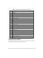
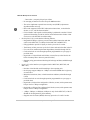
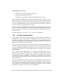
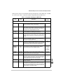
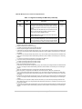
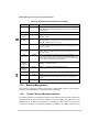
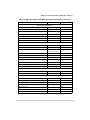
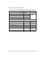
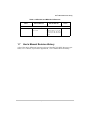
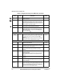
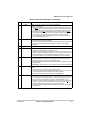
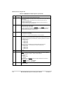
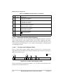
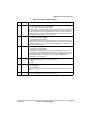
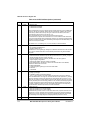
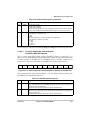
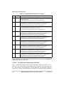
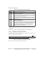
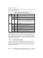
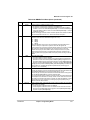
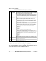
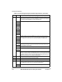
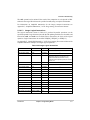
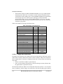
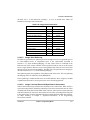
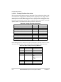
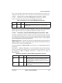
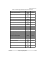
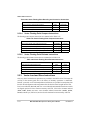
Table 2-13. L3OHCR Field Descriptions (continued)
Bits
5-7
Name
Description
L3CLK1_OH L3_CLK1 output hold. These bits configure output hold time for L3_CLK1 signal driven by the
MPC7457 to the L3 data RAMs. They should generally be set according to the SRAM’s input
hold time requirements.
See the MPC7457 Hardware Specification for specific output hold times.
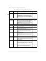
8-10
L3DOH0
L3_DATA[00:07]/L3_DP[0] output hold. These bits configure output hold time for
L3_DATA[00:07] and L3_DP[0] signals driven by the MPC7457 to the L3 data RAMs. They
should generally be set according to the SRAM’s input hold time requirements.
See the MPC7457 Hardware Specification for specific output hold times.
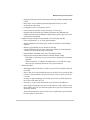
11-13
L3DOH8
L3_DATA[08:15]/L3_DP[1] output hold. These bits configure output hold time for L3_DATA[8:15]
and L3_DP[1] signals driven by the MPC7457 to the L3 data RAMs. They should generally be
set according to the SRAM’s input hold time requirements.
See the MPC7457 Hardware Specification for specific output hold times.
14-16
L3DOH16
L3_DATA[16:23]/L3_DP[2] output hold. These bits configure output hold time for
L3_DATA[16:23] and L3_DP[2] signals driven by the MPC7457 to the L3 data RAMs. They
should generally be set according to the SRAM’s input hold time requirements.
See the MPC7457 Hardware Specification for specific output hold times.
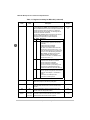
17-19
L3DOH24
L3_DATA[24:31]/L3_DP[3] output hold. These bits configure output hold time for
L3_DATA[24:31] and L3_DP[3] signals driven by the MPC7457 to the L3 data RAMs. They
should generally be set according to the SRAM’s input hold time requirements.
See the MPC7457 Hardware Specification for specific output hold times.
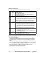
20-22
L3DOH32
L3_DATA[32:39]/L3_DP[4] output hold. These bits configure output hold time for
L3_DATA[32:39] and L3_DP[4] signals driven by the MPC7457 to the L3 data RAMs. They
should generally be set according to the SRAM’s input hold time requirements.
See the MPC7457 Hardware Specification for specific output hold times.
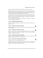
23-25
L3DOH40
L3_DATA[40:47]/L3_DP[5] output hold. These bits configure output hold time for
L3_DATA[40:47] and L3_DP[5] signals driven by the MPC7457 to the L3 data RAMs. They
should generally be set according to the SRAM’s input hold time requirements.
See the MPC7457 Hardware Specification for specific output hold times.
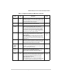
26-28
L3DOH48
L3_DATA[48:55]/L3_DP[6] output hold. These bits configure output hold time for
L3_DATA[48:55] and L3_DP[6] signals driven by the MPC7457 to the L3 data RAMs. They
should generally be set according to the SRAM’s input hold time requirements.
See the MPC7457 Hardware Specification for specific output hold times.
29-31
L3DOH56
L3_DATA[56:63]/L3_DP[7] output hold. These bits configure output hold time for
L3_DATA[56:63] and L3_DP[7]signals driven by the MPC7457 to the L3 data RAMs. They
should generally be set according to the SRAM’s input hold time requirements.
See the MPC7457 Hardware Specification for specific output hold times.
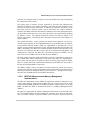
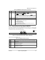
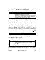
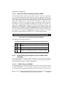
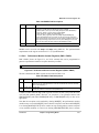
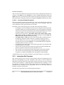
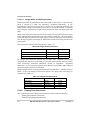
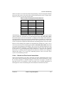
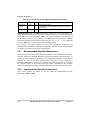
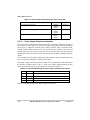
The L3OHCR register is specific to the MPC7457 and can be accessed with the mtspr and
mfspr instructions using SPR 1000.
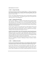
2.1.5.5.4
L3 Cache Input Timing Control (L3ITCR0)
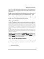
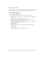
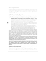
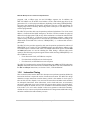
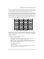
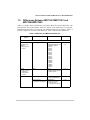
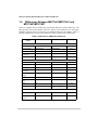
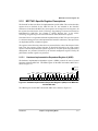
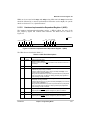
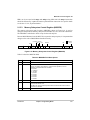
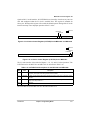
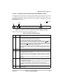
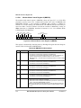
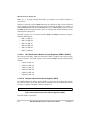
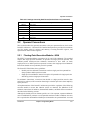
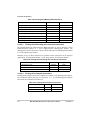
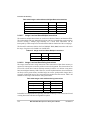
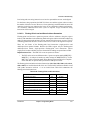
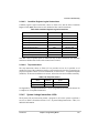
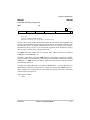
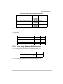
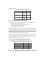
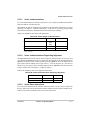
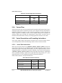
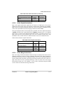
The L3 cache input timing control register (L3ITCR0), shown in Figure 2-15, is a
supervisor-level, implementation-specific SPR used to control the input AC timing of the
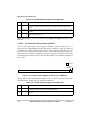
L3 cache interface of the MPC7451. For the MPC7457, the L3ITCR0, shown in
Figure 2-16, is used to control the input AC timing of L3_DATA[0:15] and L3_DP[0:1]
2-36
MPC7450 RISC Microprocessor Family User’s Manual
MOTOROLA