1
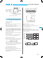
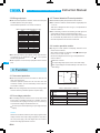
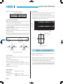
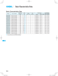
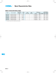
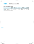
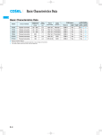
Basic Characteristics Data
Basic Characteristics Data
Model
Circuit method
Switching
frequency
[kHz]
CDS4004802
Forward converter
360
CDS4004803
Forward converter
360
CDS4004805
Forward converter
CDS4004807
CDS4004812
Material
Single
sided
Series/Parallel
operation availability
Double Series Parallel
sided operation operation
-
Aluminum
Yes
Yes
Yes
-
Aluminum
Yes
Yes
Yes
-
-
Aluminum
Yes
Yes
Yes
10 *1
-
-
Aluminum
Yes
Yes
Yes
12 *1
-
-
Aluminum
Yes
Yes
Yes
-
-
Aluminum
Yes
Yes
Yes
-
-
Aluminum
Yes
Yes
Yes
-
-
Aluminum
Yes
Yes
Yes
-
-
Aluminum
Yes
Yes
Yes
Input
current
[A]
Rated
input fuse
Inrush
current
protection
6 *1
-
9 *1
-
360
10 *1
Forward converter
360
Forward converter
360
CDS4004815
Forward converter
360
12 *1
CDS4004824
Forward converter
360
12 *1
CDS4004828
Forward converter
360
12 *1
CDS5002428H
Forward converter
360
24 *2
PCB/Pattern
CDS6002412
Forward converter
360
30 *2
-
-
Aluminum
Yes
Yes
Yes
CDS6002412H
Forward converter
360
29 *2
-
-
Aluminum
Yes
Yes
Yes
CDS6002428
Forward converter
360
30 *2
-
-
Aluminum
Yes
Yes
Yes
CDS6002428H
Forward converter
360
29 *2
-
-
Aluminum
Yes
Yes
Yes
CDS6004812
Forward converter
360
17 *1
-
-
Aluminum
Yes
Yes
Yes
CDS6004828
Forward converter
360
17 *1
-
-
Aluminum
Yes
Yes
Yes
*1 The value of input current is at DCIN48V and rated load.
*2 The value of input current is at DCIN24V and rated load.
CDS
CDS-6
DC-DC Converters Power Module type Instruction Manual
1
Pin Connection
CDS-8
2
Connection for Standard Use
CDS-8
3
Wiring Input/Output Pin
CDS-9
4
5
6
7
3.1
Wiring input pin
3.2
Wiring output pin
Function
CDS-9
CDS-10
CDS-10
4.1
Overcurrent protection
CDS-10
4.2
Overvoltage protection
CDS-10
4.3
Thermal detection/Thermal protection
CDS-10
4.4
Inverter operation monitor
CDS-10
4.5
Remote ON/OFF
CDS-11
4.6
Remote sensing
CDS-11
4.7
Adjustable voltage range
CDS-12
4.8
Isolation
CDS-12
Series and Parallel Operation
CDS-12
5.1
Series operation
CDS-12
5.2
Parallel operation/Master-slave operation
CDS-12
5.3
N+1 redundant operation
CDS-13
Implementation Mounting Method
CDS-13
6.1
Mounting method
CDS-13
6.2
Stress onto the pins
CDS-14
6.3
Cleaning
CDS-14
6.4
Soldering
CDS-14
6.5
Derating
CDS-14
Safety Considerations
CDS-14
CDS-7
CDS
DC-DC Converters Power Module type
lCDS500/600 Table 1.2 Pin Connection and function
1 Pin Connection
lCDS400
No.
CB VB TMP RC3 RC2
RC1
-VIN
Instruction Manual
-VOUT
21
TRM +S -S IOG AUX
+VIN
Pin Connection
+DC input
-VIN
-DC input
RC1
Remote ON/OFF(Input side)
+VOUT
+DC output
-VOUT
-DC output
CB
Current balance
VB
Voltage balance
TMP
Thermal detection signal
RC3
+VOUT
RC2
4-FG
lCDS500/600
CB VB TMP RC3 RC2
RC1
21
-VIN
Adjustment of output voltage
+S
+Remote sensing
21
-S
-Remote sensing
22
IOG
Inverter operation monitor
23
AUX
Auxiliary power supply
FG
Mounting hole(FG)
TRM +S -S IOG AUX
No.
+VIN
Pin Connection
+VIN
+VOUT
-VIN
RC1
4-FG
+VOUT
Fig.1.1 Pin Connection(bottom view)
CDS
lCDS400
No.
Pin Connection
4.5 ”Remote ON/OFF”
3.2 ”Wiring output pin”
5.2 ”Parallel operation/Master-slave operation”
VB
4.3 ”Thermal detection/Thermal protection”
+DC input
TMP
-DC input
RC3
RC1
Remote ON/OFF(Input side)
RC2
+VOUT
+DC output
TRM
-VOUT
-DC output
+S
CB
Current balance
21
-S
VB
Voltage balance
22
IOG
4.4 ”Inverter operation monitor”
TMP
Thermal detection signal
23
AUX
4.5 ”Remote ON/OFF”
FG
3.1 ”Wiring input pin”
Remote ON/OFF(output side)
TRM
Adjustment of output voltage
+S
+Remote sensing
-S
-Remote sensing
IOG
Inverter operation monitor
AUX
Auxiliary power supply
FG
Mounting hole(FG)
Pin Connection
-VIN
RC1
+VOUT
-VOUT
CB
VB
TMP
RC3
RC2
TRM
+S
-S
CDS-8
3.1 ”Wiring input pin”
-VIN
+VIN
21
CB
Function
Reference
+VIN
RC2
No.
-VOUT
Table 1.1 Pin Connection and function
RC3
21
Remote ON/OFF(output side)
TRM
-VOUT
23
22
Function
+VIN
Reference
3.1 ”Wiring input pin”
4.5 ”Remote ON/OFF”
3.2 ”Wiring output pin”
4.5 ”Remote ON/OFF”
4.7 ”Adjustable voltage range”
4.6 ”Remote sensing”
2 Connection for
Standard Use
nIn order to use the power supply, it is necessary to wire as shown in
Fig.2.1.
Reference: 3
6.5
”Wiring Input/Output Pin”
”Derating”
nShort the following pins to turn on the power supply.
5.2 ”Parallel operation/Master-slave operation”
4.3 ”Thermal detection/Thermal protection”
4.5 ”Remote ON/OFF”
4.7 ”Adjustable voltage range”
4.6 ”Remote sensing”
IOG
4.4 ”Inverter operation monitor”
AUX
4.5 ”Remote ON/OFF”
FG
3.1 ”Wiring input pin”
-VIN RC1, +VOUT +S, -VOUT -S
Reference: 4.5
4.6
”Remote ON/OFF”
”Remote sensing”
nThe CDS Series handles only the DC input.
Avoid applying AC input directly.
It will damage the power supply.
nOperate with the conduction cooling(e.g. heat radiation from the
aluminum base plate to the attached heat sink).
Reference: 6.5
”Derating”
Instruction Manual
Cin
DC
input
Noise
filter
+
Input voltage [V]
Heatsink
+S
+VIN
+VOUT
+
Co
-VIN
Load
-VOUT
RC1 FG
-S
2V
max
time
Cin : External capacitor on the input side
Co : External capacitor on the output side
Input voltage range
DC-DC Converters Power Module type
t
Fig.3.1 Input voltage ripple
Range of input voltage
Input current [A]
Fig.2.1 Connection for standard use
3 Wiring Input/Output Pin
lp
Input voltage [V]
3.1 Wiring input pin
Fig.3.2 Input current characteristics
(1) External fuse
nFuse is not built-in on input side. In order to protect the unit, install the normal blow type fuse on input side.
(5) Operation with AC input
nThe CDS series handles only for the DC input.
nWhen the input voltage from a front end unit is supplied to multiple units, install a regular type fuse in each unit.
A front end unit(AC/DC converter) is required when the CDS series is operated with AC input.
Table 3.1 Recommended fuse(Normal-blow type, maximum value)
Model
CDS40048
CDS50024/CDS60024
CDS60048
Rated current
30A
75A
30A
CDS
(6) Reverse input voltage protection
nAvoid the reverse polarity input voltage.It will break the power supply.
It is possible to protect the unit from the reverse input voltage by
installing an external diode.
(2) Noise filter/Decoupling capacitor
nlnstall an external noise filter for low line-noise and for stable operation of the power supply.
nlnstall a correspondence filter, if a noise standard meeting is required or if the surge voltage may be applied to the unit.
(3) External capacitor on the input side
nlnstall an external capacitor Cin between +VIN and -VIN input pins
DC
YES
CDS
Load
CDS
Load
CDS
Load
AC
NO
AC
YES
for low line-noise and for stable operation of the power supply.
AC/DC
Converter
Fig.3.3 Use with AC input
CDS40048: more than 100 F
CDS50024/CDS60024: more than 1000 F
(a)
(b)
CDS60048: more than 470 F
nWhen the line impedance is high or the input voltage rise quickly
at start-up(less than 10 s), install a capacitor Cin between +VIN
and -VIN input pins(within 50mm from pins).
+VIN
DC IN
-VIN
+VIN
DC IN
-VIN
Fig.3.4 Reverse input voltage protection
(4) Input voltage range/Input current range
nlnput voltage ripple should be less than 2Vp-p.
nMake sure that the voltage fluctuation, including the ripple voltage, will not exceed the input voltage range.
nUse a front end unit with enough power, considering the start-up
current lp of this unit.
CDS-9
DC-DC Converters Power Module type
Instruction Manual
3.2 Wiring output pin
4.3 Thermal detection/Thermal protection
nlnstall an external capacitor Co between +VOUT and -VOUT pins
nThermal detection(TMP) and protection circuit are built-in.
nWhen overheat is detected, thermal detection signal(TMP) turns
for stable operation of the power supply.
Recommended capacitance of Co is shown in Table 3.2.
”L” from ”H”.
TMP circuit is designed as shown in Fig.4.1, and specification is
Table 3.2 Recommended capacitance Co [ F]
Model
CDS4004802
CDS4004803
CDS4004805
CDS4004807
CDS4004812
CDS4004815
CDS4004824
CDS4004828
CDS5002428H
CDS6002412
CDS6002412H
CDS6002428
CDS6002428H
CDS6004812
CDS6004828
Capacitance
6800
6800
4700
4700
470
330
220
220
470
1000
1000
470
470
1000
470
shown as in Table 4.1.
nWhen overheating continues after detecting the TMP signal, the
output will be shut down by the thermal protection circuit.
When this function comes into effect, input voltage should be shut
off, and eliminate all possible causes of overheat condition and
lower the temperature of the unit to the normal level.
4.4 Inverter operation monitor
nBy using the inverter operation monitor(IOG), malfunction of the
inverter can be monitored.
When inverter operation is in following mode
nSelect the high frequency type capacitor. Output ripple and start-
CDS
,
or
, IOG signal
turns ”H” from ”L” within 1 second.
up waveform may be influenced by ESR ESL of the capacitor
lOG circuit is designed as shown in Fig.4.1and specification is
and the wiring impedance.
shown in Table 4.1.
nlnstall a capacitor Co near the output pins(within 100mm from the
Malfunction of inverter.
The output voltage drops by 60% or less of the rated voltage.
pins).
When output wattage is decreased radically to less than 10% of
rated wattage.
4 Function
22k
4.1 Overcurrent protection
TMP
or
IOG
6V typ
nOvercurrent protection is built-in and comes into effect at over
105% of the rated current.
-S
Overcurrent protection prevents the unit from short circuit and
Fig.4.1 TMP, IOG circuit
overcurrent condition. The unit automatically recovers when the
fault condition is cleared.
nWhen the output voltage drops at overcurrent, the average output
current is reduced by intermittent operation of power supply.
Table 4.1 Specification of TMP, IOG
No.
Item
1
Function
4.2 Overvoltage protection
2
Base pin
nThe overvoltage protection circuit is built-in. The DC input should
3
Level voltage ”L”
4
Level voltage ”H”
5
Maximum sink current
6
Maximum applicable voltage
be shut down if overvoltage protection is in operation. The minimum interval of DC recycling for recovery is for 2 to 3 minutes (*)
or input terminal voltage is decreased less than 1V.
The recovery time varies depending on input voltage and input
capacity.
Remarks:
Please note that devices inside the power supply might fail when
voltage more than rated output voltage is applied to output terminal of the power supply. This could happen when the customer
tests the overvoltage performance of the unit.
CDS-10
TMP
IOG
Normal operation ”H” Normal operation ”L”
Overheat detection ”L” Malfunction of inverter ”H”
-S
0.5Vmax at 5mA
5V typ
10mA max
35V max
DC-DC Converters Power Module type
Instruction Manual
nMake sure that sink current of output side remote ON/OFF circuit
4.5 Remote ON/OFF
nRemote ON/OFF circuit is built-in on both side of input(RC1) and
should be less than 12mA.
output(RC2 RC3).
(3) Auxiliary power supply for remote ON/OFF(AUX)
Output can be controlled by either circuit.
nAUX is built in for operating the output side remote ON/OFF(RC2
RC3).
(1) Input side remote ON/OFF(RC1)
nThe ground pin of input side remote ON/OFF circuit is ”-VIN” pin.
Between RC1 and -VIN: Output voltage is ON at ”Low” Ievel or
short circuit(0 - 1.0V).
Between RC1 and -VIN: Output voltage is OFF at ”High” Ievel or
If AUX is not used for RC2 RC3, AUX can be used for IOG or
TMP signal output by opto coupler.
nShort protection resistance(2.2k ) is built in.
Output voltage decreases as the output current increases.
(AUX voltage at open circuit: 16V max)
short circuit(3.5 - 7.0V).
When RC1 is ”Low” Ievel, fan out current is 0.3mA typ. When Vcc
is applied, use 3.5 Vcc 7V.
When remote ON/OFF function is not used, please short between
RC1 and -VIN.
4.6 Remote sensing
(1) When the remote sensing function is not in use
nWhen the remote sensing function is not in use, it is necessary to
confirm that pins are shorted between +S & +VOUT and between
-S & -VOUT.
Vcc
nWire between +S & +VOUT and between -S & -VOUT as short as
Rc
RC1
or
possible.
or
Loop wiring should be avoided.
This power supply might become unstable by the noise coming
-VIN
Transistor
IC
Relay
from poor wiring.
Fig.4.2 RC1 connection example
(2) When the remote sensing function is in use
nTwisted-pair wire or shield wire should be used for sensing wire.
(2)Output side remote ON/OFF(RC2 RC3)
nThick wire should be used for wiring between the power supply
Table 4.2 Specification of output side remote ON/OFF(RC2 RC3)
No.
Item
2
Function
3
Base pin
Fig.4.3 (a)
Fig.4.3 (b)
Fig.4.3 (c)
Power ON
Power ON
Power ON
”H”
”H”
”L”
-S
RC2
4
Power ON
Open
(0.1mA max)
5
Power OFF
Short
(3mA min)
(a)
(b)
2.2k
2.2k
AUX
150
RC3
13V
typ
150
RC3
RC2
OFF
RC2
POWER
ON
OFF
13V
typ
put voltage adjustment range.
nIf the sensing patterns are short, heavy-current is drawn and the
pattern may be damaged.
Short
(0.5V max)
The pattern disconnection can be prevented by installing the pro-
Open
(0.1mA max)
tection parts as close as a load.
+S
+VOUT
OUT
2.2k
AUX
150
RC3 POWER
ON
OFF
POWER
ON
-S
-S
Voltage between +VOUT and -VOUT should remain within the out-
-S and RC2
(c)
AUX
13V
typ
Line drop should be less than 0.5V.
RC2 RC3
Wiring method
1
and a load.
+
Co
Load
-VOUT
-S
Short at pin root
RC2
Fig.4.4 Connection when the remote sensing is not in use
-S
Wire as close as possible
Fig.4.3 RC2 RC3 connection example
+S
nWhen output side remote ON/OFF function is used, please short
between RC1 and -VIN.
nDo not connect RC2 and RC3 with anywhere if remote ON/OFF
is not used.
+VOUT
OUT
+
Co
Load
-VOUT
-S
Fig.4.5 Connection when the remote sensing is in use
CDS-11
CDS
DC-DC Converters Power Module type
(2) Adjusting method by applying external voltage
4.7 Adjustable voltage range
nOutput voltage is adjustable by the external potentiometer or by
nBy applying the voltage externally at TRM, output voltage become
adjustable.
applied voltage externally.
CDS5002428H, CDS6002412H, CDS6002428H : When the output voltage adjustment range is 101% or more, the input voltage
nOutput voltage is calculated by the following equation.
(Output voltage)
= (Applied voltage externally)
range is limited (Fig.4.6).
nWhen the output voltage is raised, decrease the output current so
as not to exceed the maximum output wattage.
nWhen the output voltage adjustment is used, note that the overvoltage
protection circuit operates when the output voltage sets too high.
(Rated output voltage)
4.8 Isolation
nFor a receiving inspection, such as Hi-Pot test, gradually increase
(decrease) the voltage for a start(shut down). Avoid using Hi-Pot
tester with the timer because it may generate voltage a few times
120
Output voltage [%]
Instruction Manual
114.3
higher than the applied voltage, at ON/OFF of a timer.
CDS5002428H
CDS6002428H
nBe sure to apply DC voltage when Hi-pot test is performed to the
CDS6002412H
part which is specified as DC voltage. And also set the current
110
limit of Hi-pot tester at 10mA. Don’t apply AC voltage, otherwise
101
this may damage the power supply.
100
(CDS40048 series : INPUT-OUTPUT, INPUT-FG)
18
20
19.5
22
24
20.5
Input voltage [v]
5 Series and Parallel
Operation
Fig.4.6 Input voltage derating curve
(1) Adjusting method by external resistor
nBy connecting the external potentiometer(VR1) and resistors(R1,
R2), output voltage becomes adjustable, as shown in Fig.4.6, rec-
5.1 Series operation
ommended external parts are shown in Table 4.3.
nThe wiring to the potentiometer should be as short as possible.
nSeries operation is available by connecting the outputs of two or
The temperature coefficient becomes worse, depending on the
more power supplies, as shown below. Output current in series con-
type of a resistor and potentiometer. Following parts are recom-
nection should be lower than the lowest rated current in each unit.
Metal film type, coefficient of less than 100ppm/
Potentiometer Cermet type, coefficient of less than 300ppm/
(a)
+
Power
supply
+
nWhen the output voltage adjustment is not used, open the TRM
pin and VB pin respectively.
(b)
Power
supply
-
+VOUT
RA
15k
+
Reference
voltage 2.5V
RB
10k
Power
supply
+
-
-
Fig.5.1 Examples of series operation
R2
VR1
TRM R1
+
-
+S
VB
Control Amp.
of rated
voltage
Power
supply
Load
Resistor
Load
mended for the power supply.
Load
CDS
-S
5.2 Parallel operation/Master-slave operation
-VOUT
nParallel operation is available by connecting the units as shown in
Fig.4.7 Output voltage control circuit
Fig.5.2.
nAs variance of output current drew from each power supply is
Table 4.3 Recommended value of external potentiometer & resistor
No.
Adjustable range [%] Number of unit
5
CDS-12
10
2sets
3sets
R1
36k
1k
36k
18k
12k
value determined by the following equation.
(Output current in parallel operation)
= (the rated current per unit)
24k
5k
maximum 10%, the total output current must not exceed the
R2
75k
5k
Single
4
6
2sets
3sets
3
5
VR1
Single
1
2
External parts value [ ]
910
(number of unit)
0.9
DC-DC Converters Power Module type
When the number of units in parallel operation increases, input current increase at the same time. Adequate wiring design for input
circuitry is required, such as circuit pattern, wiring and current ca-
Instruction Manual
nIOG signal might be unstable for one second when the units are
turned on in parallel operation.
nA sound may occur from power supply at parallel operating.
pacity for equipment.
5.3 N+1 redundant operation
In parallel operation, the maximum operative number of units is 11.
+VOUT
+S
VB
TRM
CB
-S
-VOUT
nIt is possible to set N+1 redundant operation for improving reliability of power supply system.
nPurpose of redundant operation is to ensure stable operation in
R2
R1
VR1
+
Co
Load
the event of single power supply failure.
Since extra power supply is reserved for the failure condition, so
total power of redundant operation is equal to N-1.
+VOUT
+S
VB
TRM
CB
-S
-VOUT
+
Co
+VOUT
+S
VB
TRM
CB
-S
-VOUT
+
Co
The output voltage
rises when VR1 is
adjusted for the
resistance between
and to lower.
6 Implementation
Mounting Method
6.1 Mounting method
nThe unit can be mounted in any direction. When two or more
power supplies are used side by side, position them with proper
intervals to allow enough air ventilation. Aluminum base plate temperature around each power supply should not exceed the temperature range shown in derating curve.
nAvoid placing the DC input line pattern lay out underneath the
Fig.5.2 Examples of parallel operation
unit, it will increase the line conducted noise. Make sure to leave
an ample distance between the line pattern lay out and the unit.
nWhen output voltage adjustment is not in use. TRM wiring, R1,
R2 and VR are not necessary.
nThick wire should be used for wiring between the power supply
and load, and line drop should be less than 0.3V.
nWhen the output-line impedance is high, the power supply is become unstable.
Use same length and thickness(width) wire(pattern) for the current balance improvement.
Also avoid placing the DC output line pattern underneath the unit
because it may increase the output noise. Lay out the pattern
away from the unit.
nHigh-frequency noise radiates directly from the unit to the atmosphere. Therefore, design the shield pattern on the printed circuit
board and connect its one to FG.
The shield pattern prevents noise radiation.
nThe maximum current is 25A per input pin and output pin.
nConnect each input pin for the lowest possible impedance.
Shield pattern
nWhen the number of the units in parallel operation increases, input current increases. Adequate wiring design for input circuitry
such as circuit pattern, wiring and current for equipment is required.
nConnect the sensing line and the power line by one point after
RC1
-VIN
-VOUT
connecting each power supply's sensing pins(+S, -S). In multiple
operation, sensing wires should be connected between each
+VIN
Shield pattern
+VOUT
units for the muster connection to a load.
nOutput current should be 10% or more of the total of the rated output current in parallel operation.
If less than 10%, the IOG signal might become unstable, and out-
Fig.6.1 Shield pattern lay out(bottom view)
put voltage slightly increasing(max5%).
CDS-13
CDS
DC-DC Converters Power Module type
nOption”-M” is available, as shown in Table 6.1.
6.5 Derating
Table 6.1 Mounting hole
nUse with the conduction cooling(e.g. heat radiation by conduction
from the aluminum base plate to the attached heat sink).
Mounting hole
Standard
3.4 thru
Optional : -M
Instruction Manual
Fig.6.3 shows the derating curve based on the aluminum base
M3 tapped
plate temperature. In the hatched area, the specification of Ripple
and Ripple Noise is different from other areas.
6.2 Stress onto the pins
100
the internal connection may be weakened.
As shown in Fig.6.2 avoid applying stress of more than 29.4N(3kgf)
on the input pins/output pins(A part) and more than 9.8N(1kgf) to
the signal pins(B part).
nThe pins are soldered on PCB internally, therefore, do not pull or
Load factor [%]
nWhen too much stress is applied to the pins of the power supply,
50
0
-20
bend them with abnormal forces.
nMounting hole diameter of PCB should be 3.5mm to reduce the
-10
0
10
20
30
40
50
60
70
80 85 90
100
Aluminum base plate temperature Tc [ ]
stress onto the pins.
nFix the unit on PCB(fixing fittings) by screws to reduce the stress
Tc:Measuring point
onto the pins. Be sure to mount the unit first, then solder the unit.
CDS
A
B
A part
A
B part
Fig.6.3 Derating curve
Less than
29.4N(3kgf)
Less than
29.4N(3kgf)
Less than
9.8N(1kgf)
Less than
9.8N(1kgf)
Less than
9.8N (1kgf)
Less than
29.4N (3kgf)
7 Safety Considerations
Fig.6.2 Stress onto the pins
nTo apply for safety standard approval using this power supply, the
following conditions must be met.
6.3 Cleaning
nClean the product with a brush. Prevent liquid from getting into
the product.
Do not soak the product into liquid.
nDo not stick solvent to a name plate or a resin case.
(If solvent sticks to a name plate or a resin case, it will cause to
change the color of the case or to fade letters on name plate
away.)
nAfter cleaning, dry them enough.
6.4 Soldering
nFlow soldering
:260
less than 15 seconds.
nSoldering iron
DC IN/DC OUT/RC1 :450
less than 5 seconds.
Signal pins
less than 3 seconds(less than 20w).
CDS-14
:350
lThis unit must be used as a component of the end-use equipment.
lThe equipment does neither contain any basic nor double/reinforced
insulation between input and output, and base plate.
If the input voltage is greater than 60VDC, this has to be provided
by the end-use equipment according to the final build in condition.
lSafety approved fuse must be externally installed on input side.