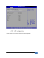
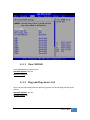
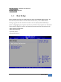
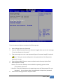
Download JetBox 8210 User Manual

Transcript
 JetBox 8150 User Manual Hardware www.korenix.com 0.0.1 Copyright Notice Copyright© 2009 Korenix Technology Co., Ltd. All rights reserved. Reproduction without permission is prohibited. Information provided in this manual is intended to be accurate and reliable. However, the original manufacturer assumes no responsibility for its use, or for any infringements upon the rights of third parties that may result from its use. The material in this document is for product information only and is subject to change without notice. While reasonable efforts have been made in the preparation of this document to assure its accuracy, Korenix assumes no liabilities resulting from errors or omissions in this document, or from the use of the information contained herein. Korenix reserves the right to make changes in the product design without notice to its users. Acknowledgments Korenix is a registered trademark of Korenix Technology Co., Ltd. All other trademarks or registered marks in the manual belong to their respective manufacturers. 2 Table of Content | Korenix Table of Content Copyright Notice ............................................................................................ 2 Acknowledgments .......................................................................................... 2 Table of Content ............................................................................................................. 3 Chapter 1 Overview ................................................................................................ 7 Chapter 2 Hardware Specification .......................................................................... 7 2‐1 Hardware Specification .......................................................................... 7 2‐2 Regulation .............................................................................................. 8 Chapter 3 Hardware Feature .................................................................................. 9 3‐1 Dimensions ............................................................................................. 9 3‐2 Front Panel Connectors ........................................................................ 10 3‐2‐1 LED Indicators ............................................................................... 10 3‐2‐2 VGA connector ............................................................................. 10 3‐2‐3 Serial Ports (COM1, COM2) .......................................................... 10 3‐2‐4 LAN Ports (LAN1, LAN2) ............................................................... 11 3‐2‐5 USB Ports ...................................................................................... 12 3‐2‐6 Audio (Mic in/Line in, Earphone‐out) .......................................... 12 3‐2‐7 DC Power & Power Switch ........................................................... 13 3‐2‐8 Reset Button ................................................................................. 14 3‐3 HW Installation ..................................................................................... 14 Chapter 4 BIOS ...................................................................................................... 17 4‐1 Main Setup ........................................................................................... 20 4‐1‐1 System memory ........................................................................... 20 4‐1‐2 System Date & Time Setup .......................................................... 21 4‐2 Advanced Setup ................................................................................... 21 4‐2‐1 CPU configuration ........................................................................ 22 4‐2‐2 IDE configuration .......................................................................... 22 4‐2‐3 SATA‐0<1>/IDE Secondary Master/Slave ..................................... 23 4‐2‐4 PATA/SATA IDE Controller ............................................................. 24 4‐2‐5 Hard Disk Write Protect ............................................................... 25 4‐2‐6 IDE Detect Time Out (Sec.) .......................................................... 25 4‐2‐7 SuperIO Chipset – Configuration .................................................. 25 4‐2‐8 Serial Port 1 Address .................................................................... 26 4‐2‐9 Serial Port 2 Address .................................................................... 26 Korenix | Table of Content 3 4‐2‐10 COMB Port Mode Selection ......................................................... 26 4‐2‐11 Hardware Health Configuration ................................................... 26 4‐2‐12 APM Configuration ....................................................................... 27 4‐2‐13 Power Manager /APM .................................................................. 28 4‐2‐14 Manual Throttle Ration ................................................................ 28 4‐2‐15 Standby Time Out ........................................................................ 29 4‐2‐16 Suspend Time Out ........................................................................ 29 4‐2‐17 Hard Disk Time Out (Minute) ....................................................... 29 4‐2‐18 Green PC Monitor Power State .................................................... 29 4‐2‐19 Video Power Down Mode ............................................................ 30 4‐2‐20 Hard Disk Power Down Mode ...................................................... 30 4‐2‐21 USB Configuration ........................................................................ 30 4‐2‐22 USB 1.1 Ports Configuration ......................................................... 31 4‐2‐23 USB 2.0 Ports Enable .................................................................... 31 4‐2‐24 Legacy USB Support ..................................................................... 32 4‐2‐25 USB 2.0 Controller Mode ............................................................. 32 4‐2‐26 BIOS ECHI Hand‐Off ...................................................................... 32 4‐3 PCIPnP Setup ........................................................................................ 32 4‐3‐1 Clear NVRAM ................................................................................ 33 4‐3‐2 Plug and Plug Aware O/S .............................................................. 33 4‐3‐3 PCI Latency Timer ........................................................................ 34 4‐3‐4 Palette Snoop ............................................................................... 34 4‐3‐5 PCI IDE BusMaster ........................................................................ 34 4‐3‐6 IRQ 3 –15 ...................................................................................... 34 4‐4 Boot Setup ............................................................................................ 35 4‐4‐1 Boot Setting Configuration ........................................................... 36 4‐4‐2 Quick Boot .................................................................................... 36 4‐4‐3 Boot Up Num‐Lock ....................................................................... 37 4‐4‐4 PS/2 Mouse Support ..................................................................... 37 4‐4‐5 Wait for ‘F1’ If Error ..................................................................... 37 4‐4‐6 Hit ‘DEL’ Message Display ............................................................ 37 4‐4‐7 Boot Device .................................................................................. 38 4‐4‐8 First /Second /Third Hard Disk Boot Device ................................. 38 4‐4‐9 Hard Disk Drives ........................................................................... 39 4‐4‐10 Removable Drives ......................................................................... 39 4‐5 Security setup ...................................................................................... 40 4‐5‐1 Clear User Password ..................................................................... 42 4 Table of Content | Korenix 4‐5‐2 assword Check .............................................................................. 42 4‐5‐3 Boot Sector Virus Protection ....................................................... 42 4‐1 Chipset Setup ....................................................................................... 43 4‐1‐1 Northbridge VIA CX700 Configuration ......................................... 43 4‐1‐2 DRAM Clock/Timing Configuration .............................................. 44 4‐1‐3 AGP & P2P Bridge Configuration .................................................. 44 4‐1‐4 Southbridge VIA CX700 Configuration ......................................... 45 4‐1‐5 High Definition Audio ................................................................... 45 4‐1‐6 PCI Delayed Transaction ............................................................... 46 4‐1‐7 On Board LAN1/2 Controller ......................................................... 46 4‐1‐8 LAN Boot ROM Controller ............................................................ 46 Chapter 5 Software Installation ............................................................................ 46 5‐1 VIA HyperionPro Driver ........................................................................ 46 5‐2 VGA Drivers .......................................................................................... 47 5‐3 Audio Drivers ........................................................................................ 48 5‐4 LAN Utility & Driver .............................................................................. 48 5‐5 Watchdog Timer .................................................................................. 48 5‐6 Programming RS‐485 ........................................................................... 52 5‐6‐1 Initialize COM port ....................................................................... 53 5‐6‐1 Send out one character (Transmit) .............................................. 53 5‐6‐2 Send out one block data (Transmit – the data more than two characters) .................................................................................................... 54 5‐6‐3 Receive data ................................................................................. 54 5‐6‐4 Basic Language Example .............................................................. 54 Chapter 6 Technical Reference ............................................................................. 55 6‐1 Real‐Time Clock and Non‐Volatile RAM ............................................... 55 6‐2 CMOS RAM Map .................................................................................. 57 6‐3 I/O Port Address Map........................................................................... 58 6‐4 Interrupt Request Lines (IRQ) ............................................................... 59 6‐5 DMA Channel Map ............................................................................... 59 6‐6 Serial Ports ........................................................................................... 60 6‐7 Receiver Buffer Register (RBR) ............................................................. 61 6‐8 Transmitter Holding Register (THR)...................................................... 61 6‐9 Interrupt Enable Register (IER) ............................................................. 61 6‐10 Interrupt Identification Register (IIR) ................................................... 61 6‐11 Line Control Register (LCR) ................................................................... 62 6‐12 MODEM Control Register (MCR) .......................................................... 62 Korenix | Table of Content 5 6‐13 6‐14 6‐15 Chapter 7 7‐1 7‐2 Line Status Register (LSR) ..................................................................... 63 MODEM Status Register (MSR) ............................................................ 63 Divisor Latch (LS, MS) ........................................................................... 63 Appendix .............................................................................................. 64 Notes .................................................................................................... 64 Customer Service ................................................................................. 65 6 Table of Content | Korenix Chapter 1 Overview Industrial X86 1GHz Multimedia Computer The advantage of adopting Korenix JetBox series is ready‐to‐use. Korenix is devoted to improve the usability of embedded computer in industrial domain. Korenix integrates device drivers, protocol stacks, system utilities, supporting services for Windows XP embedded in a CompactFlash card or in a 2.5” HD installed in the JetBox 8150 to let users experience JetBox 8150 in a simple way. The JetBox 8150 is a VIA Eden V4 1GHz based computer with system memory 1GB DDRII RAM and built in media processor for multimedia performance enhancement. Volume and performance of the JetBox 8150 is utilized as a perfect front end device: compact design, DiN‐rail type mouting, and carrying all major interfaces, such as two USB2.0 ports, one RS‐232 port, one RS‐232/422/485 port, VGA, and high resolution audio. In addition, it is equipped with two RJ‐45 ports and supports web server services to accommodate to the network communication environment today. Chapter 2 Hardware Specification 2­1 Hardware Specification Model JetBox 8510 CPU VIA Eden(V4) 1GHz VIA CX700M 1 DDR2 So‐DIMM (Max.) 1GB RTC Battery backup external RTC Battery 3V Li‐Battery WDT Internal Watch Dog Timer VGA 1 Audio Ear‐Phone, MIC‐In(default) or Line‐In Korenix | Overview 7 COM port RS232 *1, RS232/422/485 * 1 USB Host USB v2.0 Host Port * 2 Ethernet Realtek RTL8100C 10/100 Base‐T * 2 CF Card slot 1 SATA HDD slot 1 Power Switch 1 LED Indicator Power * 1, HD * 1 Reset Button 1 Power Input 12VDC‐24VDC 2‐pin terminal block or power jack Power Consumption 16W +12~+24V DC, 1.26A maximum (0.82A typical) with DC 19V input. Construction Rugged Aluminum Alloy Chassis, IP31 protection Color Silver Mounting DIN rail Dimensions 50(W)*145(H)*102(D)mm Operating Temperature ‐15℃ ~ 70℃, 5 to 95% RH Net Weight 700g Table 1 JetBox 8150 HW specification 2­2 Regulation Regulation: FCC class A, CE EN55022 class A EN55024 EN61000‐3‐2, 3 EN61000‐4‐2, 3, 4, 5, 6, 8, 11 IEC 60950 IEC 61373 Shock: IEC60068‐2‐27 (50g peak acceleration) Vibration: IEC60068‐2‐6 (5g/ 10~150Hz/operating) MTBF: 76,493 hours MIL‐HDBK‐217F (MILITARY HANDBOOK) standard Warranty: 5 years 8 Hardware Specification | Korenix
Chapter 3 Hardware Feature 3­1 Dimensions 102
Following is the mechanical outline for JetBox 8150. 50.4
145
Picture 1 JetBox 8150 mechanical outline Korenix | Hardware Feature 9 3­2 Front Panel Connectors 3­2­1 LED Indicators The Power and HDD LED’s has two distinctive statuses: Off for inactive operation and blinking light for activity. 3­2­2 VGA connector DB15 Signal 1 Red 2 Green 3 Blue 13 Hsync 14 Vsync 12 DDC Data 15 DDC Clock 5 & 10 Digital Ground 6,7,8 Analog Ground Others Not Used Note 1: Resolution CRT mode: 2048 x 1536 @ 32 bpp (75 Hz) LCD / Simultaneous (CRT+LVDS LCD): 1600 x 1200 DVI: 1600 x 1200 3­2­3 Serial Ports (COM1, COM2) The DB9 (COM1/2) is standard serials port connector. The following tables show the 10 Hardware Feature | Korenix signal connections of these connectors. Pin RS‐232 RS‐422 RS‐485 No#
1 DCD 2 RxD RxD‐(A) Data‐(A)
3 TxD RxD+(B) Data+(B)
4 DTR 5 GND 6 DSR 7 RTS TxD‐(A) 8 CTS TxD+(B) 9 RI The COM1 is RS‐232 and the COM2 is designed for multiple proposes. Use JP1 selects the RS‐232, RS‐422 or RS‐485. The default setting of COM2 is RS‐232. 3­2­4 LAN Ports (LAN1, LAN2) The RJ45 connector with 2 LED’s for LAN. The right side LED (orange) indicates data is being accessed and the left side LED (green) indicates on‐line status. (On indicates on‐line and off indicates off‐line). Korenix | Hardware Feature 11 RJ45 LAN1/2 RJ45 LAN1/2
1 TPTX+ 5 FBG 2 TPTX ‐ 6 TPRX ‐
3 TPRX+ 7 FBG 4 FBG FBG 8 3­2­5 USB Ports The JetBox supports a four port USB connector. Any USB device can be attached to USB ports with plug‐and‐play supported. USB#1/2 Signal
Pin 1 USBV
Pin 2 USBD‐
Pin 3 USBD+
Pin 4 USBG
3­2­6 Audio (Mic in/Line in, Earphone­out) Connect the Audio Microphone In/Line‐in, Earphone‐out. JP4 & JP5 is to select Line‐In or Mic‐In of Mic‐In connector. The default setting is Mic‐in. 12 Hardware Feature | Korenix 3­2­7 DC Power & Power Switch Power is supplied through an external AC/DC power adapter or power DC In. Check the technical specification section for information about AC/DC power input voltage. See following figure and a side pictures. 1.
DC‐Power Jack: Use External AC/DC power adapter DC +12V~+24V, 30W minimum Since the switch does include a power switch, plugging its power adapter into a power outlet then switch power to on, when you final installed system hardware device. On: Power On Off: Power Off 2.
DC Power Connector: Use external 2‐pin apart able terminal block. (Please see Korenix | Hardware Feature 13 the spots circled.) DC12~24V
Terminal Block 3­2­8 Reset Button The FX5311 has a push button switcher for system reset; Push and release the button will cause hardware reset of FX5311 and restart system booting. 3­3 HW Installation Before Installation Before you install the system, make sure you follow the following descriptions. 1. Before removing the cover, shut down the operation System and disconnect power switch to off and unplug AC‐to DC Adapter cable. 2. Install any connector, Compact Flash, and hard disk is sure that the power is disconnected or power switch to off from the system. If not, this may damage the system. 3. The ESD (Electricity Static Discharge) may be created from human body that touches the board. It may do damage to the board circuit. Removing Covers –Installing Hardware If you are installing hardware option, you can remove the front and back cover. The 14 Hardware Feature | Korenix following figure will guide you how to install 2.5" HDD inside, Compact Flash modules, and DDR2‐RAM module. a. Unscrew front cover and Installing Compact Flash Note 2: The Compact Flash socket supports Compact Flash Modules and Micro Drives. b. Unscrew back cover and Installing Hard Disk b1. Installing Hard Disk Korenix | Hardware Feature 15 Note 3: Use caution when handling the hard disk to prevent damage to SATA connector as you inserted hard disk. Be careful with the orientation when installing connectors. c. Installing Memory: So‐DIMM Socket for DDR2 RAM Modules You may extend additional memory to the JetBox, See as following figure and rear pictures. The So‐DIMM socket supports 512MB to 1GB of DDR2 RAM modules. 16 Hardware Feature | Korenix Chapter 4 BIOS BIOS are a program located on a Flash memory chip on a circuit board. It is used to initialize and set up the I/O peripherals and interface cards of the system, which includes time, date, hard disk drive, the ISA bus and connected devices such as the video display, diskette drive, and the keyboard. This program will not be lost when you turn off the system. The BIOS provides a menu‐driven interface to the console subsystem. The console subsystem contains special software, called firmware that interacts directly with the hardware components and facilitates interaction between the system hardware and the operating system. The BIOS default values ensure that the system will function at its normal capability. In the worst situation the user may have corrupted the original settings set by the manufacturer. All the changes you make will be saved in the system RAM and will not be lost after power‐off. When you start the system, the BIOS will perform a self‐diagnostics test called Power On Self Test (POST) for all the attached devices, accessories, and the system. Press the [Del] key to enter the BIOS Setup program, and then the main menu will show on the screen. Note 4: Change the parameters when you fully understand their functions and subsequence. Korenix | BIOS 17 BIOS Functions On the menu, you can perform the following functions 1. Main 2. Advanced ¾ CPU Configuration ¾ IDE Configuration ¾ SuperIO Configuration ¾ Hardware Health Configuration ¾ APM Configuration ¾ USB Configuration 3. PCIPnP 4. Boot ¾ Boot Settings Configuration ¾ Boot Device Priority ¾ Hard Disk Drives ¾ CD/DVD Drivers 5. Security 18 BIOS | Korenix ¾ Change Supervisor Password ¾ Change User Password ¾ Clear User Password ¾ Boot Sector Virus Protection 6. Chipset ¾ NorthBridge VIA CX700 Configuration ¾ SouthBridge VIA CX700 Configuration 7. Exit ¾ Save Changes and Exit: Exit system setup after saving the changes.F10 key can be used for this operation. ¾ Discard Changes and Exit: Exit system setup without saving any changes. ESC key can be used for this operation. ¾ Discard Changes: Discard changes down so far any of the set questions. F7 key can be used this operation. ¾ Load Optimized Default: to auto configure the system according to optimal setting with pre‐defined values. This is also the factory default setting of the system when you receive the board. ¾ Load Fail‐Safe Default: to configure the system in fail‐safe mode with predefined values. Keyboard Convention On the BIOS, the following keys can be used to operate and manage the menu: Item Function
ESC To exit the current menu or message Page Up/Page Down To select a parameter F1 To display the help menu if you do not know the purpose or function of the item you are going to configure F8 Fail‐Safe Default F9 Optimized Default F10
Save and exit
Korenix | BIOS 19 UP/Down Arrow Keys To go upward or downward to the desired item 4­1 Main Setup This section describes basic system hardware configuration, system clock setup and BIOS version information. If the CPU board is already installed in a working system, you will not need to select this option anymore. 4­1­1 System memory This option is display‐only which is determined by POST (Power On Self Test) of the BIOS. 20 BIOS | Korenix 4­1­2 System Date & Time Setup Highlight the <Date> field and then press the [Page Up] / [Page Down] or [+]/ [‐] keys to set the current date. Follow the month, day and year format. Highlight the <Time> field and then press the [Page Up] / [Page Down] or [+]/ [‐] keys to set the current date. Follow the hour, minute and second format. The user can bypass the date and time prompts by creating an AUTOEXEC.BAT file. For information on how to create this file, please refer to the MS‐DOS manual. 4­2 Advanced Setup Select the Advanced tab from the setup screen to enter the Advanced BIOS Setup screen. You can select any of the items in the left frame of the screen, such as SuperIO Configuration, to go to the sub menu for that item. You can display an Advanced BIOS Setup option by highlighting it using the <Arrow> keys. All Advanced BIOS Setup options are described in this section. The Advanced BIOS Setup screen is shown below. The sub menus are described on the following pages. Korenix | BIOS 21 4­2­1 CPU configuration You can use this screen to select options for the CPU information. Use the up and down <Arrow> keys to select an item. Use the <Plus> and <Minus> keys to change the value of the selected option. Note 5: The CPU Configuration setup screen varies depending on the installed processor. 4­2­2 IDE configuration You can use this screen to select options for the IDE Configuration Settings. Use the up and down <Arrow> keys to select an item. Use the <Plus> and <Minus> keys to change the value of the selected option. A description of the selected item appears on the right side of the screen. The settings are described on the following pages. An example of the IDE Configuration screen is shown below. 22 BIOS | Korenix 4­2­3 SATA­0<1>/IDE Secondary Master/Slave IDE hard drive controllers can support up to two separate hard drives. These drives have a master/slave relationship, which is determined by the cabling configuration used to attach them to the controller. Your system supports one IDE controller – a primary – so you have the ability to install up to two separate hard disks. LBA/Large Mode LBA (Logical Block Addressing) is a method of addressing data on a disk drive. In LBA mode, the maximum drive capacity is 137 GB. The Optimal and Fail‐Safe default setting is Auto Hard Disk Type The BIOS supports various types for user settings, The BIOS supports <Pri Master>, <Pri Slave>, so the user can install up to two hard disks. For the master and slave jumpers, please refer to the hard disk’s installation descriptions and the hard disk jumper settings. You can select <AUTO> under the <TYPE> and <MODE> fields. This will Enabled Korenix | BIOS 23 auto detection of your IDE drives during boot up. This will allow you to change your hard drives (with the power off) and then power on without having to reconfigure your hard drive type. If you use older hard disk drives, which do not support this feature, then you must configure the hard disk drive in the standard method as described above by the <USER> option. PIO MODE PIO means Programmed Input/Output. Rather than have the BIOS issue a series of commands to affect a transfer to or from the disk drive, PIO allows the BIOS to tell the controller what it wants and then let the controller and the CPU perform the complete task by them. This is simpler and more efficient (and faster). Your system supports five modes, numbered from 0 to 4, which primarily differ in timing. When Auto is selected, the BIOS will select the best available mode. BLOCK (Multi‐Sector Transfer) This option allows your hard disk controller to use the fast block mode to transfer data to and from your hard disk drive (HDD). S.M.A.R.T This field is used to activate the S.M.A.R.T (System Management and Reporting Technologies) function for S.M.A.R.T HDD drives. This function requires an application that can give S.M.A.R.T message. 32 Bit Data Transfer This option sets the 32‐bit data transfer option. The Optimal and Fail‐Safe default setting is enabled. 4­2­4 PATA/SATA IDE Controller This item specifies the ATA/IDE channels used by the onboard PATA/SATA IDE controller. Available Options: SATA, IDE, Disabled, and Both Default setting: Both 24 BIOS | Korenix 4­2­5 Hard Disk Write Protect Set this option to protect the hard disk drive from being overwritten. The Optimal and Fail‐Safe default setting is disabled. Available Options: Disabled, Enabled Default setting: Disabled 4­2­6 IDE Detect Time Out (Sec.) Set this option to stop the AMIBIOS from searching for IDE devices within the specified number of seconds. Basically, this allows you to fine‐tune the settings to allow for faster boot times. Adjust this setting until a suitable timing that can detect all IDE disk drives attached is found. Available Options: 0, 5, 10, 15, 20, 25, 30, and 35 Default setting: 35 4­2­7 SuperIO Chipset – Configuration ITE8712 Super IO Chipset This section describes the function of Super I/O settings. Korenix | BIOS 25 4­2­8 Serial Port 1 Address These fields select the I/O port address for each Serial port. Available Options: Disabled, 3F8H/IRQ4, 3E8H/IRQ4, 2F8H/IRQ4 and 2E8H/IRQ3. Default setting: 3F8H/IRQ4 4­2­9 Serial Port 2 Address These fields select the I/O port address for each Serial port. Available Options: Disabled, 3F8H/IRQ4, 3E8H/IRQ4, 2F8H/IRQ4 and 2E8H/IRQ3. Default setting: 2F8H/IRQ3 4­2­10 COMB Port Mode Selection These fields item can select RS‐232, RS‐422 and RS‐485 of select port 2. Available Options: RS‐232, RS‐422 and RS485 Default setting: RS‐232 4­2­11 Hardware Health Configuration On the Hardware Monitor Setup screen, you can monitor the system temperature, CPU voltage, and VCC voltage… 26 BIOS | Korenix 4­2­12 APM Configuration You can use this screen to select options for the USB Configuration. Korenix | BIOS 27 4­2­13 Power Manager /APM Select Enabled to activate the chipset Power Management and APM (Advanced Power Management) features. Available Options: Disabled and Enabled Default setting: Enabled 4­2­14 Manual Throttle Ration In a power management state, the BIOS can throttle the CPU clock to reduce power consumption. For example, a throttle ratio of 50% means the clock is turned off half of its normal operational time. Available Options: 0~6.25%, 18.75~25%, 50%~56.25%, 75%~87.5%, and up to 97.5% Default setting: 50%~56.25% 28 BIOS | Korenix 4­2­15 Standby Time Out This field specifies the length of a period of system inactivity (like hard disk or video) while in full power on state. When this length of time expires, the system enters Standby power state. Available Options: Disabled, 1 Minute, 2 Minute, 4 Minute, and 8 Minute, up to 60 Minute. Default setting: Disabled 4­2­16 Suspend Time Out This field specifies the length of time the system waits before it enters suspend mode. Available Options: Disabled, 1 Minute, 2 Minute, 4 Minute, and 8 Minute, up to 60 Minute. Default setting: Disabled 4­2­17 Hard Disk Time Out (Minute) This option specifies the amount of time the hard disk drive can be inactive before the computer enters a power‐conserving state specified in the Hard Disk Drive Power Down Mode option. Available Options: Disabled, 1 Minute, 2 Minute, and 3 Minute, up to 15 Minute. Default setting: Disabled 4­2­18 Green PC Monitor Power State This option specifies the power state that the green PC‐compliant video monitor enters when the BIOS places it in a power saving state after the specified period of display inactivity has expired. Available Options: Standby, Suspend, and Off Default setting: Off Korenix | BIOS 29 4­2­19 Video Power Down Mode This field specifies the power conserving state that video subsystem enters after the specified period of display inactivity has expired. Available Options: Disabled, Standby, Suspend Default setting: Disabled 4­2­20 Hard Disk Power Down Mode This field specifies the power conserving state that the hard disk drive enters after the specified period of hard drive inactivity has expired. Available Options: Disabled, Standby, Suspend Default setting: Disabled 4­2­21 USB Configuration You can use this screen to select options for the USB Configuration. 30 BIOS | Korenix 4­2­22 USB 1.1 Ports Configuration Set this value to allow the system to Enabled or Disabled the onboard USB ports. The Optimal and Fail‐Safe default setting is 2 USB Ports. Available Options: USB 2 Ports, and Disabled Default setting: USB 2 Ports 4­2­23 USB 2.0 Ports Enable This field is Enables USB controllers. Select Enabled, if a USB device is installed to the system. If Disabled are selected, the system will not be able to use a USB device. Available Options: Enabled, and Disabled Default setting: Enabled Korenix | BIOS 31 4­2­24 Legacy USB Support Legacy USB Support refers to the USB mouse and USB keyboard support. Normally if this option is not enabled; any attached USB mouse or USB keyboard will not become available until a USB compatible operating system is fully booted with all USB drivers loaded. When this option is enabled, any attached USB mouse or USB keyboard can control the system even when there is no USB drivers loaded on the system. Set this value to Enabled or Disabled the Legacy USB Support. Available Options: Disabled, Enabled and AUTO Default setting: Auto 4­2­25 USB 2.0 Controller Mode This field is configures the USB 2.0 controllers in High speed (480Mbps) or Full speed (12Mbps). Available Options: HiSpeed and FullSpeed Default setting: Hispeed 4­2­26 BIOS ECHI Hand­Off This is a workaround for OS without ECHI Hand‐Off support. The ECHI ownership change should claim by ECHI driver. Available Options: Enabled and Disabled Default setting: Enabled 4­3 PCIPnP Setup Select the PCI/PnP tab from the setup screen to enter the Plug and Play BIOS Setup screen. You can display a Plug and Play BIOS Setup option by highlighting it using the <Arrow> keys. All Plug and Play BIOS Setup options are described in this section. The Plug and Play BIOS Setup screen is shown below. 32 BIOS | Korenix 4­3­1 Clear NVRAM Clear NVRAM during system boot. Available Options: Yes, No Default setting: No 4­3­2 Plug and Plug Aware O/S Set to Yes to inform BIOS that the operating system can handle Plug and Play (PnP) devices. Available Options: Yes, No Default setting: No Korenix | BIOS 33 4­3­3 PCI Latency Timer This field specifies the latency timings (in PCI clock) PCI devices installed in the PCI expansion bus. Available Options: 32, 64, 96, 128, 160,192, 224, and 248 Default setting: 64 4­3­4 Palette Snoop When Enabled is selected, multiple VGA devices operating on different buses can handle data from the CPU on each set of palette registers on every video device. Bit 5 of the command register in the PCI device configuration space is the VGA Palette Snoop bit. (0 is disabled). Available Options: Disabled: Data read and written by the CPU is only directed to the PCI VGA devices palette registers. Enabled: Data read and written by the CPU is directed to both the PCI VGA devices palette registers. Default setting: Disabled 4­3­5 PCI IDE BusMaster This option is to specify that the IDE controller on the PCI local bus have bus‐mastering capability. Available Options: Enabled, Disabled Default setting: Disabled 4­3­6 IRQ 3 –15 When I/O resources are controlled manually, you can assign each system interrupt as one of the following types, based on the type of device using the interrupt: Available: Specified IRQ is available to the used by PCI/PnP devices. Reserved: Specified IRQ is reserved for used by Legacy ISA devices. 34 BIOS | Korenix Available Options: Available and Reserved Default setting: Available 4­4 Boot Setup Select the Boot tab from the setup screen to enter the Boot BIOS Setup screen. You can select any of the items in the left frame of the screen, such as Boot Device Priority, to go to the sub menu for that item. You can display a Boot BIOS Setup option by highlighting it using the <Arrow> keys. All Boot Setup options are described in this section. Select an item on the Boot Setup screen to access the sub menu for: • Boot Setting Configuration • Boot Device Priority • Hard disk drives • Removable Drivers Korenix | BIOS 35 4­4­1 Boot Setting Configuration 4­4­2 Quick Boot This field is used to activate the quick boot function of the system. When set to Enabled, 1. BIOS will not wait for up to 40 seconds if a Ready signal is not received from the IDE drive, and will not configure its drive. 2. BIOS will not wait for 0.5 seconds after sending a RESET signal to the IDE drive. 3. You cannot run BIOS Setup at system boot since there is no delay for the Hit, Del. To run Setup message. Available Options: Disabled, Enabled Default setting: Enabled 36 BIOS | Korenix 4­4­3 Boot Up Num­Lock This field is used to activate the Num Lock function upon system boot. If the setting is on, after a boot, the Num Lock light is lit, and user can use the number key. Available options: On, Off Default setting: On 4­4­4 PS/2 Mouse Support The PS/2 mouse function is optional. Before you configure this field, make sure your system board supports this feature. The setting of Enabled allows the system to detect a PS/2 mouse on boot up. If detected, IRQ12 will be used for the PS/2 mouse. IRQ 12 will be reserved for expansion cards if a PS/2 mouse is not detected. Disabled will reserve IRQ12 for expansion cards and therefore the PS/2 mouse will not function. Available options: Disabled, Enabled and Auto Default setting: Auto 4­4­5 Wait for ‘F1’ If Error AMIBIOS POST error messages are followed by: Press <F1> to continue If this field is set to Disabled, the AMIBIOS does not wait for you to press the <F1> key after an error message. Available options: Disabled, Enabled Default setting: Disabled 4­4­6 Hit ‘DEL’ Message Display Set this field to Disabled to prevent the message as follows: Hit ‘DEL’ if you want to run setup It will prevent the message from appearing on the first BIOS screen when the computer boots. Korenix | BIOS 37 Available options: Disabled, Enabled Default setting: Enabled 4­4­7 Boot Device Use this screen to specify the order in which the system checks for the device to boot from. To access this screen, select Boot Device Priority on the Boot Setup screen and press <Enter>. 4­4­8 First /Second /Third Hard Disk Boot Device Set the boot device options to determine the sequence in which the computer checks which device to boot from. The settings are Removable Dev., Hard Drive, or 38 BIOS | Korenix ATAPI CDROM. Note 6: When you select a boot category from the boot menu, a list of devices in that category appears. For example, if the system has three hard disk drives connected, then the list will show all three hard disk drives attached 4­4­9 Hard Disk Drives Use this screen to view the hard disk drives in the system. To access this screen, select Hard disk drives on the Boot Setup screen and press <Enter>. 4­4­10 Removable Drives Use this screen to view the removable drives in the system. To access this screen, select removable drives on the Boot Setup screen and press <Enter>. Korenix | BIOS 39 4­5 Security setup There are two security passwords: Supervisor and User. Supervisor is a privileged person that can change the User password from the BIOS. According to the default setting, both access passwords are not set up and are only valid after you set the password from the BIOS. • Change Supervisor Password • Change User Password • Clear User Password • Boot Sector Virus Protection 40 BIOS | Korenix To set the password, please complete the following steps. 1.
2.
3.
Select Change Supervisor Password. Type the desired password (up to 6 character length) when you see the message, “Enter New Supervisor Password.” Then you can go on to set a user password (up to 6 character length) if required. Note 7: that you cannot configure the User password until the Supervisor password is set up. 4. Enter Advanced BIOS Features screen and point to the Security Option field. 5. Select System or Setup. i.Always: a visitor who attempts to enter BIOS or operating system will be prompted for password. ii.Setup: a visitor who attempts to the operating system will be prompted for user password. You can enter either User password or Supervisor password. 6. Point to Save Settings and Exit and press Enter. Korenix | BIOS 41 Press Y when you see the message, “Save Current Settings and Exit (Y/N)?” Note 8: it is suggested that you write down the password in a safe place to avoid that password may be forgotten or missing. 4­5­1 Clear User Password Select Clear User Password from the Security Setup menu and press <Enter>. Clear New Password > [Ok] [Cancel] appears. Type the password and press <Enter>. The screen does not display the characters entered. Retype the password as prompted and press <Enter>. 4­5­2 assword Check This field enables password checking every time the computer is powered on or every time the BIOS Setup is executed. If Always is chosen, a user password prompt appears every time and the BIOS Setup Program executes and the computer is turned on. If Setup is chosen, the password prompt appears if the BIOS executed. Available options: Setup, Always Default setting: Setup 4­5­3 Boot Sector Virus Protection This option is near the bottom of the Security Setup screen. The Optimal and Fail‐Safe default setting is disabled Enabled: Set this value to prevent the Boot Sector Virus Protection. This is the default setting. Disabled: Select Enabled to enable boot sector protection, displays a warning when any program (or virus) issues a Disk Format command or attempts to write to the boot sector of the hard disk drive. If enabled, the following appears when a write is attempted to the boot sector. You may have to type N several times to prevent the boot sector write. Boot Sector Write! 42 BIOS | Korenix Possible VIRUS: Continue (Y/N)? _ The following appears after any attempt to format any cylinder, head, or sector of any hard disk drive via the BIOS INT 13 Hard disk drive Service: Format!!! Possible VIRUS: Continue (Y/N)? 4­1 Chipset Setup This section describes the configuration of the board’s chipset features. • NorthBridge VIA CX700 Configuration • SouthBridge VIA CX700 Configuration 4­1­1 Northbridge VIA CX700 Configuration You can use this screen to select options for the North Bridge Configuration. Use the up and down <Arrow> keys to select an item. Use the <Plus> and <Minus> keys to Korenix | BIOS 43 change the value of the selected option. 4­1­2 DRAM Clock/Timing Configuration DRAM Timing If the installed SDRAM supports SPD function, select auto. If not, you can select based on other access time of the SDRAM. Available Options: Auto, Manual, Turbo and Ultra Default setting Auto 4­1­3 AGP & P2P Bridge Configuration Onchip VGA Configuration VGA Frame Buffer Size This field is share memory architecture (SMA) for frame buffer memory. SMA allows system memory to be efficiently share by the host CPU and allocated depending on user preference, application requirements, and total size of system memory. 44 BIOS | Korenix Available Options: Disabled, 16MB,32MB, 64MB and 128MBA Default setting: 32MBU V‐ LINKAGP & PCI Bus Configuration Timing PCI Master 0WS Write This field specifies the PCI Master 0 wait state installed in the PCI expansion bus. Available Options: Disabled and Enabled Default setting: Enabled U 4­1­4 Southbridge VIA CX700 Configuration You can use this screen to select options for the South Bridge Configuration. South Bridge is a chipset on the motherboard that controls the basic I/O functions, LAN port, and audio function. 4­1­5 High Definition Audio This field specifies the internal Audio Control. Available Options: Disabled, and Auto Default setting: Auto Korenix | BIOS 45 4­1­6 PCI Delayed Transaction This field specifies the chipset has an embedded 32‐bit posted write buffer to support delay transactions cycles. Select Enabled to support compliance with PCI specification version 2. Available Options: Disabled, and Enabled Default setting: Enabled 4­1­7 On Board LAN1/2 Controller This field specifies the Enabled or Disabled of the onboard LAN chip. Available Options: Disabled, and Enabled Default setting: Enabled 4­1­8 LAN Boot ROM Controller This field specifies the PXE boot ROM of the onboard LAN chip. Available Options: Disabled, and Enabled Default setting: Disabled Chapter 5 Software Installation 5­1 VIA HyperionPro Driver WIN 2000/XP Driver Installs VIA Chipset, IRQ Routing, AGP Driver, SATA HDD driver and PCI IDE Bus Master 4in 1Driver. Step 1 Execute SETUP.exe file. Step 2 46 Software Installation | Korenix
The screen shows the SETUP type. Press any key to enter the main menu. Step 3 As the setup is completed, the system will generate the message as follows. Yes, I want to restart my computer now. Installation is done! No, I will restart my computer later. System must be restart then complete the installation 5­2 VGA Drivers WIN 2000/XP Driver Step 1 Execute SETUP.EXE file. Step 2 The screen shows the SETUP type. Press any key to enter the main menu. Step 3 As the setup is completed, the system will generate the message as follows. Yes, I want to restart my computer now. Installation is done! No, I will restart my computer later. System must be restart then complete the installation. Step 4 In the WINDOWS XP/2K, you can find the <DISPLAYL> icon located in the {CONTROL PANEL} group. Step 5 Adjust the <Color>,<Font size> and <Resolution>. Korenix | Software Installation 47 5­3 Audio Drivers WIN 2000/XP Driver Step 1 Execute setup.exe file. Step 2 The screen shows the SETUP type. Press any key to enter the main menu. Step 3 As the setup is completed, the system will generate the message as follows. Yes, I want to restart my computer now. Installation is done! No, I will restart my computer later. System must be restart then complete the installation. 5­4 LAN Utility & Driver Step 1 Execute install.exe file. Note 9: In the RTL8139C directory, a README.TXT is included to provide installation information. 5­5 Watchdog Timer This section describes how to use the Watchdog Timer, including disabled, enabled, and trigger functions. The JetBox is equipped with a programmable time‐out period watchdog timer. You can use your own program to Enabled the watchdog timer. Once you have enabled the watchdog timer, the program should trigger the I/O every time before the timer times out. If your program fails to trigger or disable this timer before it times out, e.g. 48 Software Installation | Korenix
because of a system hang‐up, it will generate a reset signal to reset the system. The time‐out period can be programmed to be set from 1 to 255 seconds or minutes. Watchdog Timer Setting The watchdog timer is a circuit that may be used from your program software to detect system crashes or hang‐ups. The watchdog timer is automatically disabled after reset. Once you have enabled the watchdog timer, your program must trigger the watchdog timer every time before it times out. After you trigger the watchdog timer, it will be set to non‐zero value to watchdog counter and start to count down again. If your program fails to trigger the watchdog timer before time‐out, it will generate a reset pulse to reset the system. The factor of the watchdog timer time‐out constant is approximately 1 second. The period for the watchdog timer time‐out is between 1 to FF timer factors. If you want to reset your system when watchdog times out, the following table listed the relation of timer factors between time‐out periods. Time Factor Time‐Out Period (Seconds) Time‐Out Period (Minutes) 1 1 1 2 2 2 3 3 3 4 4 4 5 5 5 “ “ “ “ “ “ “ “ “ Korenix | Software Installation 49 FF FF FF Watchdog Timer Enabled To Enabled the watchdog timer, you have to output a byte of timer factor to the watchdog register whose address is 2Eh and data port is 2fH. The following is an Assemble program, which demonstrates how to enable the watchdog timer and set the time‐out period at 28 seconds. ;‐‐‐‐‐‐‐‐‐‐‐‐‐‐‐‐‐‐‐‐‐‐‐‐‐‐‐‐‐‐‐‐‐‐‐‐‐‐‐‐‐‐‐‐‐‐‐‐‐‐‐‐‐‐‐‐‐‐‐‐‐‐‐‐‐‐‐‐‐‐‐‐‐‐‐‐‐‐‐‐‐‐‐‐‐‐‐‐‐‐ ; Enter the extended function mode, interruptible double‐write ;‐‐‐‐‐‐‐‐‐‐‐‐‐‐‐‐‐‐‐‐‐‐‐‐‐‐‐‐‐‐‐‐‐‐‐‐‐‐‐‐‐‐‐‐‐‐‐‐‐‐‐‐‐‐‐‐‐‐‐‐‐‐‐‐‐‐‐‐‐‐‐‐‐‐‐‐‐‐‐‐‐‐‐‐‐‐‐‐‐‐ Mov dx, 2eh ; Enter to extended function mode Mov al, 87h Out dx,al Out dx,al Mov al,07h Out dx,al ;‐‐‐‐‐‐‐‐‐‐‐‐‐‐‐‐‐‐‐‐‐‐‐‐‐‐‐‐‐‐‐‐‐‐‐‐‐‐‐‐‐‐‐‐‐‐‐‐‐‐‐‐‐‐‐‐‐‐‐‐‐‐‐‐‐‐‐‐‐‐‐‐‐‐‐‐‐‐‐‐‐‐‐‐‐‐‐‐‐‐‐‐‐‐‐‐‐‐‐‐‐‐ ; Logical device 8, configuration register CRF5 Bit 3,CRF6 Bit 0~7 ;‐‐‐‐‐‐‐‐‐‐‐‐‐‐‐‐‐‐‐‐‐‐‐‐‐‐‐‐‐‐‐‐‐‐‐‐‐‐‐‐‐‐‐‐‐‐‐‐‐‐‐‐‐‐‐‐‐‐‐‐‐‐‐‐‐‐‐‐‐‐‐‐‐‐‐‐‐‐‐‐‐‐‐‐‐‐‐‐‐‐‐‐‐‐‐‐‐‐‐‐‐‐ Mov dx,2fh Mov al,08h ; Select Logical Device 8 of watchdog timer Out dx,al Mov dX,2eh Mov al,0f5h ;Set second as counting unit Out dx,al Mov dx,2fh In al,dx …
50 Software Installation | Korenix
Or al,c0 ; Trigger P/W LED. And al,not c8h ;Set Second. ;And al,c8h ;Set Minute. Out dx,al Mov dx,2eh Mov al,0f6h Out dx,al Mov dx,2fh Mov al,28h ; Set timeout interval as 28seconds and start counting Out dx,al ;‐‐‐‐‐‐‐‐‐‐‐‐‐‐‐‐‐‐‐‐‐‐‐‐‐‐‐‐‐‐‐‐‐‐‐‐‐‐‐‐‐‐ ; Exit extended function mode ;‐‐‐‐‐‐‐‐‐‐‐‐‐‐‐‐‐‐‐‐‐‐‐‐‐‐‐‐‐‐‐‐‐‐‐‐‐‐‐‐‐‐ Mov dx,2eh Mov al,0aah Out dx,al …
Watchdog Timer Trigger After you enabled the watchdog timer, your program must write the same factor as enabling to the watchdog register at least once every time‐out period to its previous setting. You can change the time‐out period by writing another timer factor to the watchdog register at any time, and you must trigger the watchdog before the new time‐out period in next trigger. …
Watchdog Timer Disabled To Disabled the watchdog timer, simply write a 00H to the watchdog register. ;‐‐‐‐‐‐‐‐‐‐‐‐‐‐‐‐‐‐‐‐‐‐‐‐‐‐‐‐‐‐‐‐‐‐‐‐‐‐‐‐‐‐‐‐‐‐‐‐‐‐‐‐‐‐‐‐‐‐‐‐‐‐‐‐‐‐‐‐‐‐‐‐‐‐‐‐‐‐‐‐‐‐‐‐‐‐‐‐‐‐ ; Enter the extended function mode, interruptible double‐write ;‐‐‐‐‐‐‐‐‐‐‐‐‐‐‐‐‐‐‐‐‐‐‐‐‐‐‐‐‐‐‐‐‐‐‐‐‐‐‐‐‐‐‐‐‐‐‐‐‐‐‐‐‐‐‐‐‐‐‐‐‐‐‐‐‐‐‐‐‐‐‐‐‐‐‐‐‐‐‐‐‐‐‐‐‐‐‐‐‐‐ Mov dx,2eh ; Enter to extended function mode Mov al,87h Out dx,al Out dx,al ;‐‐‐‐‐‐‐‐‐‐‐‐‐‐‐‐‐‐‐‐‐‐‐‐‐‐‐‐‐‐‐‐‐‐‐‐‐‐‐‐‐‐‐‐‐‐‐‐‐‐‐‐‐‐‐‐‐‐‐‐‐‐‐‐‐‐‐‐‐‐‐‐‐‐‐‐‐‐‐‐‐‐‐‐‐‐‐‐‐‐‐‐‐‐‐‐‐‐‐‐‐‐‐‐‐‐‐‐‐‐‐‐
‐‐‐‐‐‐‐‐ ; Logical device 8, configuration register CRF5 Bit 3(Sec./Min.), CRF6 Bit 0~7 (Count.) ;‐‐‐‐‐‐‐‐‐‐‐‐‐‐‐‐‐‐‐‐‐‐‐‐‐‐‐‐‐‐‐‐‐‐‐‐‐‐‐‐‐‐‐‐‐‐‐‐‐‐‐‐‐‐‐‐‐‐‐‐‐‐‐‐‐‐‐‐‐‐‐‐‐‐‐‐‐‐‐‐‐‐‐‐‐‐‐‐‐‐‐‐‐‐‐‐‐‐‐‐‐‐‐‐‐‐‐‐‐‐‐‐
Korenix | Software Installation 51 ‐‐‐‐‐‐‐‐ Mov al,07h Out dx,al Mov dx,2fh Mov al,08h ; Select Logical Device 8 of watchdog timer Out dx,al Mov dX,2eh Mov al,0f5h ;Set second as counting unit Out dx,al Mov dx,2fh In al,dx And al,not c8h ;Set Second or Minute. Out dx,al Mov dx,2eh Mov al,0f6h Out dx,al Mov dx,2fh Mov al,00h ; Set Watchdog Timer Disabled Out dx,al ;‐‐‐‐‐‐‐‐‐‐‐‐‐‐‐‐‐‐‐‐‐‐‐‐‐‐‐‐‐‐‐‐‐‐‐‐‐‐‐‐‐‐ ; Exit extended function mode ;‐‐‐‐‐‐‐‐‐‐‐‐‐‐‐‐‐‐‐‐‐‐‐‐‐‐‐‐‐‐‐‐‐‐‐‐‐‐‐‐‐‐ Mov dx,2eh ;Exit the extended function mode Mov al,0aah Out dx,al 5­6 Programming RS­485 The majority communicative operation of the RS‐485 is in the same of the RS‐232. When the RS‐485 precedes the transmission, which needs control the TXC signal, and the installing, steps are as follows: Step 1: Enabled TXC Step 2: Send out data 52 Software Installation | Korenix
Step 3: Waiting for data empty Step 4: Disabled TXC Note 10: Please refer to the section of the “Serial Ports” in the Chapter 6 “Technical Reference” for the detail description of the COM ports register. 5­6­1 Initialize COM port Step 1: Initialize COM port in the receiver interrupt mode, and /or transmitter interrupt mode. (All of the communication protocol buses of the RS‐485 are in the same.) Step 2: Disabled TXC (transmitter control), the bit 0 of the address of offset+4 just sets “0”. Note 11: Control the JetBox system “DTR” signal to the RS‐485 TXC communication. 5­6­1 Send out one character (Transmit) Step 1: Enabled TXC signal, and the bit 0 of the address of offset+4 just sets “1”. Step 2: Send out the data. (Write this character to the offset+0 of the current COM port address) Step 3: Wait for the buffer’s data empty. Check transmitter holding register (THRE, bit 5 of the address of offset+5), and transmitter shift register (TSRE, bit 6 of the address of offset+5) are all sets must be “0”. Korenix | Software Installation 53 Step 4: Disabled TXC signal, and the bit 0 of the address of offset+4 sets “0” 5­6­2 Send out one block data (Transmit – the data more than two characters) Step 1: Enabled TXC signal, and the bit 0 of the address of offset+4 just sets “1”. Step 2: Send out the data. (Write all data to the offset+0 of the current COM port address) Step 3: Wait for the buffer’s data empty. Check transmitter holding register (THRE, bit 5 of the address of offset+5), and transmitter shift register (TSRE, bit 6 of the address of offset+5) are all sets must be “0”. Step 4: Disabled TXC signal, and the bit 0 of the address of offset+4 sets “0” 5­6­3 Receive data The RS‐485’s operation of receiving data is in the same of the RS‐232’s. 5­6­4 Basic Language Example a. Initial 86C450 UART 10 OPEN “COM1:9600,m,8,1”AS #1 LEN=1 20 REM Reset DTR 30 OUT &H3FC, (INP(%H3FC) AND &HFA) 40 RETURN b. Send out one character to COM1 54 Software Installation | Korenix
10 20 30 40 50 60 70 80 90 REM Enabled transmitter by setting DTR ON OUT &H3FC, (INP(&H3FC) OR &H01) REM Send out one character PRINT #1, OUTCHR$ REM Check transmitter holding register and shift register IF ((INP(&H3FD) AND &H60) >0) THEN 60 REM Disabled transmitter by resetting DTR OUT &H3FC, (INP(&H3FC) AND &HEF) RETURN c. Receive one character from COM1
10 20 30 40 50 60 70 80 REM Check COM1: receiver buffer IF LOF(1)<256 THEN 70 REM Receiver buffer is empty INPSTR$” RETURN REM Read one character from COM1: buffer INPSTR$=INPUT$(1,#1) RETURN Note 12: The RS‐485 of the JetBox uses COM2. If you want to program it and hardware setup, please refer to the BIOS Setup for COM2 address setup. Chapter 6 Technical Reference 6­1 Real­Time Clock and Non­Volatile RAM The JetBox contains a real‐time clock compartment that maintains the date and time in addition to storing configuration information about the computer system. It contains 14 bytes of clock and control registers and 114 bytes of general purpose RAM. Because of the use of CMOS technology, it consumes very little power and can be maintained for long periods of time using an internal Lithium battery. The Korenix | Technical Reference 55 contents of each byte in the CMOS RAM are listed below: Address Description 00 Seconds 01 Second alarm 02 Minutes 03 Minute alarm 04 Hours 05 Hour alarm 06 Day of week 07 Date of month 08 Month 09 Year 0A Status register A 0B Status register B 0C Status register C 0D Status register D 0E Diagnostic status byte 0F Shutdown status byte 10 Diskette drive type byte, drive A and B 11 Fixed disk type byte, drive C 12 Fixed disk type byte, drive D 13 Reserved 14 Equipment byte 15 Low base memory byte 16 High base memory byte 17 Low expansion memory byte 18 High expansion memory byte 19‐2D Reserved 2E‐2F 2‐byte CMOS checksum 30 Low actual expansion memory byte 31 High actual expansion memory byte 32 Date century byte 33 Information flags (set during power on) 34‐7F Reserved for system BIOS 56 Technical Reference | Korenix
6­2 CMOS RAM Map Register Description 00h ‐10h Standard AT‐compatible RTC and Status and Status Register data definitions 11h – 13h Varies 14h Equipment Bits 7‐6 Number of Floppy Drives 00 1 Drive 01 2 Drives Bits 5‐4 Monitor Type 00 Not CGA or MDA 01 40x25 CGA 01 2 Drives 80x25 CGA Bits 3 Display Enabled 0 Disabled 1 Enabled Bit 2 Keyboard Enabled 00 Not CGA or MDA 01 40x25 CGA 01 2 Drives 80x25 CGA Bit 1 Math Coprocessor Installed 0 Absent 1 Present Bit 0 Floppy Drive Installed 0 Disabled 1 Enabled 15h Base Memory (in 1KB increments), Low Byte 16h Base Memory (in 1KB increments), High Byte 17h IBM‐compatible memory (in 1KB increments), Low Byte 18h IBM‐compatible memory (in 1KB increments), High Byte (max 15 MB) 19h‐2Dh Varies 2Eh Standard CMOS RAM checksum, high byte 2Fh Standard CMOS RAM checksum, low byte Korenix | Technical Reference 57 30h IBM‐compatible Extended Memory, Low Byte (POST) in KB 31h IBM‐compatible Extended Memory, High Byte (POST) in KB 32h Century Byte 33h Reserved. Do not use 34h Reserved. Do not use 35h Low byte of extended memory (POST) in 64 KB 36h High byte of extended memory (POST) in 64 KB 37h‐3Dh Varies 3Eh Extended CMOS Checksum, Low Byte (including 34h‐3Dh) 3Fh Extended CMOS Checksum, High Byte (including 34h‐3Dh) 6­3 I/O Port Address Map Each peripheral device in the system is assigned a set of I/O port addresses, which also becomes the identity of the device. There is a total of 1K‐port address space available. The following table lists the I/O port addresses used on the Industrial CPU Card. Address Device Description 000h ‐ 01Fh
DMA Controller #1 020h ‐ 03Fh
Interrupt Controller #1 040h ‐ 05Fh
Timer 060h ‐ 06Fh
Keyboard Controller 070h ‐ 071h
Real Time Clock, NMI 080h ‐ 09Fh
DMA Page Register 0A0h ‐ 0BFh Interrupt Controller #2 0C0h ‐ 0DFh DMA Controller #2 0F0h Clear Math Coprocessor Busy Signal
0F1h Reset Math Coprocessor 1F0h ‐ 1F7h
IDE Interface 2E8h – 2EFh Serial Port #4(COM4) 2F8h ‐ 2FFh
Serial Port #2(COM2) 58 Technical Reference | Korenix
3E8h – 3EFh Serial Port #3(COM3) 3F8h ‐ 3FFh
6­4 Serial Port #1(COM1) Interrupt Request Lines (IRQ) There are a total of 15 IRQ lines available on the Industrial CPU Card. Peripheral devices use interrupt request lines to notify CPU for the service required. The following table shows the IRQ used by the devices on the Industrial CPU Card. Level Function IRQ0 System Timer Output
IRQ1 Keyboard IRQ2 Interrupt Cascade IRQ3 Serial Port #2 IRQ4 Serial Port #1 IRQ5 USB#0 IRQ6 Reserved IRQ7 USB#1 IRQ8 Real Time Clock IRQ9 SM‐BUS IRQ10 LAN#1 IRQ11 USB#2/LAN#2/VGA IRQ12 USB#3/PS2 Mouse IRQ13 FPU IRQ14 Primary IDE IRQ15 Secondary IDE (CF) 6­5 DMA Channel Map The equivalents of two 8237A DMA controllers are implemented in the FX5311 board. Each controller is a four‐channel DMA device that will generate the memory addresses and control signals necessary to transfer information directly between a peripheral device and memory. This allows high speeding information transfer with less CPU intervention. The two DMA controllers are internally cascaded to provide four DMA channels for transfers to 8‐bit peripherals (DMA1) and three channels for transfers to 16‐bit peripherals (DMA2). DMA2 channel 0 provides the cascade Korenix | Technical Reference 59 interconnection between the two DMA devices, thereby maintaining IBM PC/AT compatibility. The following is the system information of DMA channels: DMA Controller 1 DMA Controller 2 Channel 0: Spare Channel 4: Cascade for controller 1 Channel 1: Reserved for IBM SDLC Channel 5: Spare Channel 2: Diskette adapter Channel 6: Spare Channel 3: Spare Channel 7: Spare 6­6 Serial Ports The ACEs (Asynchronous Communication Elements ACE1 to ACE2) are used to convert parallel data to a serial format on the transmit side and convert serial data to parallel on the receiver side. The serial format, in order of transmission and reception, is a start bit, followed by five to eight data bits, a parity bit (if programmed) and one, one and half (five‐bit format only) or two stop bits. The ACEs are capable of handling divisors of 1 to 65535, and produce a 16x clock for driving the internal transmitter logic. Provisions are also included to use this 16x clock to drive the receiver logic, also included in the ACE a completed MODEM control capability, and a processor interrupt system that may be software tailored to the computing time required to handle the communications link. The following table is a summary of each ACE accessible register DLAB Port Address 0 Register Base + 0 Receiver buffer (read) Transmitter holding register (write) 0 Base + 1 Interrupt enable X Base + 2 Interrupt identification (read only)
60 Technical Reference | Korenix
X Base + 3 Line control X Base + 4 MODEM control X Base + 5 Line status X Base + 6 MODEM status X Base + 7 Scratched register 1 Base + 0 Divisor latch (least significant byte) 1 Base + 1 Divisor latch (most significant byte) 6­7 Receiver Buffer Register (RBR) Bit 0‐7: Received data byte (Read Only) 6­8 Transmitter Holding Register (THR) Bit 0‐7: Transmitter holding data byte (Write Only) 6­9 Interrupt Enable Register (IER) Bit 0: Enable Received Data Available Interrupt (ERBFI) Bit 1: Enable Transmitter Holding Empty Interrupt (ETBEI) Bit 2: Enable Receiver Line Status Interrupt (ELSI) Bit 3: Enable MODEM Status Interrupt (EDSSI) Bit 4: Must be 0 Bit 5: Must be 0 Bit 6: Must be 0 Bit 7: Must be 0 6­10 Interrupt Identification Register (IIR) Bit 0: “0” if Interrupt Pending Bit 1: Interrupt ID Bit 0 Bit 2: Interrupt ID Bit 1 Korenix | Technical Reference 61 Bit 3: Must be 0 Bit 4: Must be 0 Bit 5: Must be 0 Bit 6: Must be 0 Bit 7: Must be 0 6­11 Line Control Register (LCR) Bit 0: Word Length Select Bit 0 (WLS0) Bit 1: Word Length Select Bit 1 (WLS1) WLS1 WLS0 Word Length 0 5 Bits 0 1 6 Bits 1 0 7 Bits 1 1 8 Bits 0 Bit 2: Number of Stop Bit (STB) Bit 3: Parity Enable (PEN) Bit 4: Even Parity Select (EPS) Bit 5: Stick Parity Bit 6: Set Break Bit 7: Divisor Latch Access Bit (DLAB) 6­12 MODEM Control Register (MCR) Bit 0: Data Terminal Ready (DTR) Bit 1: Request to Send (RTS) Bit 2: Out 1 (OUT 1) Bit 3: Out 2 (OUT 2) Bit 4: Loop Bit 5: Must be 0 Bit 6: Must be 0 Bit 7: Must be 0 62 Technical Reference | Korenix
6­13 Line Status Register (LSR) Bit 0: Data Ready (DR) Bit 1: Overrun Error (OR) Bit 2: Parity Error (PE) Bit 3: Framing Error (FE) Bit 4: Break Interrupt (BI) Bit 5: Transmitter Holding Register Empty (THRE) Bit 6: Transmitter Shift Register Empty (TSRE) Bit 7: Must be 0 6­14 MODEM Status Register (MSR) Bit 0: Delta Clear to Send (DCTS) Bit 1: Delta Data Set Ready (DDSR) Bit 2: Training Edge Ring Indicator (TERI) Bit 3: Delta Receive Line Signal Detect (DSLSD) Bit 4: Clear to Send (CTS) Bit 5: Data Set Ready (DSR) Bit 6: Ring Indicator (RI) Bit 7: Received Line Signal Detect (RSLD) 6­15 Divisor Latch (LS, MS) LS MS Bit 0: Bit 0 Bit 8 Bit 1: Bit 1 Bit 9 Bit 2: Bit 2 Bit 10 Bit 3: Bit 3 Bit 11 Bit 4: Bit 4 Bit 12 Bit 5: Bit 5 Bit 13 Bit 6: Bit 6 Bit 14 Bit 7: Bit 7 Bit 15 Korenix | Technical Reference 63 Desired Baud Rate Divisor Used to Generate 16x Clock 300 384 600 192 1200 96 1800 64 2400 48 3600 32 4800 24 9600 12 14400 8 19200 6 28800 4 38400 3 57600 2 115200 1 Chapter 7 Appendix 7­1 Notes Note 1: Resolution ....................................................................................... 10 Note 2: The Compact Flash socket supports Compact Flash Modules and Micro Drives. ........................................................................................ 15 Note 3: Use caution when handling the hard disk to prevent damage to SATA connector as you inserted hard disk. Be careful with the orientation when installing connectors. ................................................. 16 64 Appendix | Korenix Note 4: Change the parameters when you fully understand their functions and subsequence. ................................................................................ 17 Note 5: The CPU Configuration setup screen varies depending on the installed processor. ............................................................................... 22 Note 6: When you select a boot category from the boot menu, a list of devices in that category appears. For example, if the system has three hard disk drives connected, then the list will show all three hard disk drives attached ..................................................................................... 39 Note 7: that you cannot configure the User password until the Supervisor password is set up. ............................................................................... 41 Note 8: it is suggested that you write down the password in a safe place to avoid that password may be forgotten or missing. .............................. 42 Note 9: In the RTL8139C directory, a README.TXT is included to provide installation information........................................................................ 48 Note 10: Please refer to the section of the “Serial Ports” in the Chapter 6 “Technical Reference” for the detail description of the COM ports register. ................................................................................................. 53 Note 11: Control the JetBox system “DTR” signal to the RS‐485 TXC communication. ................................................................................... 53 Note 12: The RS‐485 of the JetBox uses COM2. If you want to program it and hardware setup, please refer to the BIOS Setup for COM2 address setup. ................................................................................................... 55 7­2 Customer Service Korenix Technologies Co., Ltd. usiness service: [email protected] Customer service: [email protected] Korenix | Appendix 65