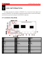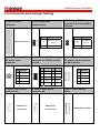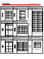
1
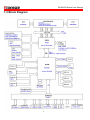
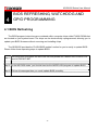
AR-B5432 Series User Manual
AR-B5432 Board
EPIC SBC supports Intel ATOM N270 Processor
with Dual Gigabit LANs / LCD / TV out / DVI
User Manual
Manual Rev.: 1.0
Book Number: AR-B5432-2010.12.17
1
AR-B5432 Series User Manual
Revision
Version
Date
Author
Description
1.0
2009.08.06 Roger
Initial release.
1.01
2010.12.17 Roger
Modified the manual descirption
2
AR-B5432 Series User Manual
Copyright 2010
All Rights Reserved.
Manual’s first edition:
For the purpose of improving reliability, design and function, the information in this document is
subject to change without prior notice and does not represent a commitment on the part of the
manufacturer.
In no event will the manufacturer be liable for direct, indirect, special, incidental, or
consequential damages arising out of the use or inability to use the product or documentation, even
if advised of the possibility of such damages.
This document contains proprietary information protected by copyright. All rights are reserved.
No part of this manual may be reproduced by any mechanical, electronic, or other means in any
form without prior written permission of the manufacturer.
Trademarks
AR-B5432 is a registered trademarks of Acrosser; IBM PC is a registered trademark of the
International Business Machines Corporation; Pentium is a registered trademark of Intel
Technologies Inc; Award is a registered trademark of Award Software International Inc; other
product names mentioned herein are used for identification purposes only and may be trademarks
and/or registered trademarks of their respective companies.
3
AR-B5432 Series User Manual
Table of Contents
1 Introduction ......................................................................................... 5
1.1 Specifications .....................................................................................................................6
1.2 Package Contents ..............................................................................................................7
1.3 Block Diagram ....................................................................................................................8
2 H/W Information .................................................................................. 9
2.1 Locations (Top Side) ..........................................................................................................9
2.2 Locations (Bottom Side)..................................................................................................10
2.3 Connector and Jumper Setting....................................................................................... 11
3 BIos Setting ....................................................................................... 15
3.1 Main Setup ........................................................................................................................16
3.2 Advanced Setup ...............................................................................................................17
3.3 Power Setup .....................................................................................................................18
3.4 PnP/PCI Setup ..................................................................................................................19
3.5 Peripherals Setup.............................................................................................................20
3.6 PC Health Setup ...............................................................................................................21
3.7 Boot Setup ........................................................................................................................22
3.8 Exit Setup..........................................................................................................................23
4 BIOS Refreshing, WatchDog and GPIO Programming .................. 25
4.1 BIOS Refreshing...............................................................................................................25
4.2 WatchDog Programming .................................................................................................26
4.3 GPIO Programming ..........................................................................................................30
5 Electrical Characteristics ................................................................. 35
5.1 Basic Electrical Characteristics Table............................................................................35
4
AR-B5432 Series User Manual
1
INTRODUCTION
Welcome to the AR-B5432 Computer. The AR-B5432 is a Intel 945GSE chipset based
platform designed for low power consumption and wide operating temperature. It supports the
Atom N270 processor, while coming with a 533MHz Front Side Bus.
5
AR-B5432 Series User Manual
1.1 Specifications
Processor: on-board Intel Atom N270
Single core and supports 2-Threads.
1.6GHz core frequency.
533MHz FSB.
512KBs L2 cache.
2.5W low TDP.
Chipset-North Bridge: Intel 945GSE
One SODIMM socket supports DDRⅡ 533/400 SODIMM and capacity up to 1GBs max.
DVMT 3.0 supports 224MBs graphics memory max. (shared with system memory).
Analog display supports 400MHz/256-bit RAMDAC, resolution QXGA
(2048x1536@75Hz).
18-bits LVDS supports Single/Dual channel LCD, resolution UXGA (1600x1200).
DVI-D supports 165MHz pixel rate max., resolution UXGA (1600x1200).
Chipset-South Bridge: Intel 82801GM
Two SATAⅡ connectors.
AC’97 Codec ALC655 supports 5.1 CH. audio output.
Two PCI-e GbE controllers - Intel 82574L - support 1000/100/10 Mbps LANs.
Six USB2.0 ports.
Supports +3.3V CompactFlash TypeⅡ card with Ultra-DMA mode 2/1/0.
PCI-104 supports four PCI devices with PCI Bus Master mode.
Super I/O: F81865F-I
Internal WatchDog, programmable 1~255 second(s)/minute(s).
8 bits programmable bi-direction GPIOs, TTL-3.3V.
Four serial ports, one supports RS232/485/422.
One Serial Infrared (SIR), baud rate 115.2K bps max. (optional).
Two DC fan connectors, one supports ON/OFF control by system temperature.
Hardware monitor for voltage, fan speed and temperature.
Others
Power requirement: +12Vdc input only ([email protected] typically).
Operating temperature: 0~60℃ (32~140℉).
Storage temperature: -40~85℃ (-40~185℉).
Relative humidity: 0~90%@40℃ (104℉), non-condensing.
Dimension: 165 mm x 115 mm.
6
AR-B5432 Series User Manual
1.2 Package Contents
Check if the following items are included in the package.
AR-B5432 EPIC SBC board
Quick Manual
Software Utility CD
7
AR-B5432 Series User Manual
1.3 Block Diagram
8
AR-B5432 Series User Manual
2
H/W INFORMATION
This chapter describes the installation of AR-B5432. First, it shows the function diagram and
the layout of AR-B5432. Then describes the unpacking information which you should read carefully,
as well as the jumper/switch settings for the AR-B5432 configuration.
2.1 Locations (Top Side)
CN2
LVDS1
PWR2
JP2
CN7
PWR1
JP3
GPIO1
VGA1
PWR5
JP5
CN1
CN4
AUDIO1
LAN1
PWR3
SYSFAN1
LAN2
SATA1
COM1
CN3
SATA2
COM4
CN8
BAT1
COM3
LED1
IR1
COM2
CPUFAN1
CN6
DVI-D1
9
AR-B5432 Series User Manual
2.2 Locations (Bottom Side)
SODIMM1
SKT1
CF1
10
AR-B5432 Series User Manual
2.3 Connector and Jumper Setting
1. CN2: PCI-104
connector.
3. JP3: Signal SERIRQ
connects to PCI-104 pin #B1
selection.
2. JP2: CMOS data
retention/clear.
STATUS
SETTING
STATUS
CMOS data retention.
PCI-104 connector.
1-2
Disconnected.
Open
(Default).
2-3
4. PWR5: External +12V
DC power input
connector.
SETTING
(Default)
CMOS data reset.
5. CN4: Internal USB2.0
connector for USB2.0 port #3,
port #4.
Short
Connected.
6. PWR3: Extra +12V and +5V
DC power output connector
(for SATA device).
PIN SETTING PIN SETTING
PIN
1
2
3
4
SETTING
1
+5V
2
+5V
3
USB3-
4
USB4-
5
USB3+
6
USB4+
7
GND
8
GND
9
GND
10
GND
GND
GND
+12V
+12V
7. SATA1: SATA device
connector #1.
8. SATA2: SATA device
connector #2.
SATA device
SATA device
connector #1.
connector #2.
11
PIN
SETTING
1
+12V
2
GND
3
+3.3V
4
+5V
9. BAT1: CMOS battery
holder.
CMOS battery holder.
AR-B5432 Series User Manual
10. IR1: Infrared device
connector. (Optional)
11. CN6: RS422/RS485 signal
connector.
PIN
PIN
12. LVDS1: LCD panel (LVDS,
18-bit/36-bit) connector.
SETTING
SETTING
PIN
SETTING
PIN
SETTING
1
LCD VDD
2
GND
3
E CLK-
4
E CLK+
5
GND
6
E Data2-
7
E Data2+
8
GND
9
E Data1-
10
E Data1+
11
NC
12
NC
13
E Data0+
14
E Data0-
15
GND
16
O CLK+
17
O CLK-
18
GND
19
O Data2+
20
O Data2-
21
I2C CLK
22
O Data1+
23
O Data1-
24
I2C Data
25
O Data0+
26
O Data0-
27
NC
28
NC
29
LCD VDD
30
LCD VDD
RS485 DATA+
1
+3.3V
1
or RS422 TX+
2
NC
RS485 DATA-
3
2
IR RX
or RS422 TX4
5
GND
RS422 RX+
4
RS422 RX-
IR TX
13. CN7: Front panel
connector. (NOTE 1)
STATUS
3
14. GPIO1: 8-bit TTL-3.3V GPIO
connector.
SETTING
External buzzer.
PIN SETTING PIN SETTING
1
1: Buzz +
2
1
+3.3V
2
GND
3
GPIO [50]
4
GPIO [54]
5
GPIO [51]
6
GPIO [55]
7
GPIO [52]
8
GPIO [56]
9
GPIO [53]
10
GPIO [57]
2: Buzz 3-4
Hardware reset
Power button for
ATX mode;
5-6
jumper opened
E: Even for dual channel.
O: Odd for single channel.
for AT mode.
15. JP5: COM2 function RS232/RS422/RS485 selection.
STATUS
16. AUDIO1: 5.1 channels Audio
signal connector.
17. SYSFAN1: System DC fan
connector.
SETTING
PIN
SETTING
PIN SETTING
PIN
SETTING
1
GND
2
+12V
3
Fan speed data
COM2 as
1 Line-out Right 2 Line-out Left
1-2
RS232.
3
AGND
4
AGND
(Default)
5
Line-in Right
6
Line-in Left
COM2 as
7
MIC-in
8
AGND
RS422.
9
AGND
10
AGND
3-4
COM2 as
5-6
11 SR-out Right 12 SR-out Left
13
LFT-out
RS485.
12
14
SEN-out
ON/OFF controlled by
system temperature setting
of BIOS.
AR-B5432 Series User Manual
18. COM1: D-SUB-9 male
connector for RS232 port #1.
19. COM4: RS232 signal
connector for port #4.
20. COM3: RS232 signal
connector for port #3.
PIN SETTING PIN SETTING
PIN SETTING PIN SETTING
1
DCD #4
2
DSR #4
1
DCD #3
2
DSR #3
D-SUB-9 male connector
3
RX #4
4
RTS #4
3
RX #3
4
RTS #3
for RS232 port #1.
5
TX #4
6
CTS #4
5
TX #3
6
CTS #3
7
DTR #4
8
RI #4
7
DTR #3
8
RI #3
9
GND
10
NC
9
GND
10
NC
21. COM2: RS232 signal
connector for port #2.
22. DVI-D1: DVI-D signal
output connector.
PIN SETTING PIN SETTING
23. PWR2: LCD panel driving
voltage selection.
PIN SETTING PIN
SETTING
1
GND
2
Data 0+
3
Data 0-
4
GND
5
Data 1+
6
Data 1-
7
GND
8
Data 2+
1
DCD #2
2
DSR #2
9
Data 2-
10
GND
3
RX #2
4
RTS #2
11
CLK +
12
CLK -
STATUS
SETTING
+3.3V for LCD panel.
1-2
5
TX #2
6
CTS #2
13
DPD
14
I2C CLK
7
DTR #2
8
RI #2
15
+5V
16
I2C Data
9
GND
10
NC
17
NC
18
GND
19
NC
20
GND
21
NC
22
GND
23
NC
24
NC
25
NC
26
NC
24. PWR1: LCD panel inverter
power connector.
25. VGA1: D-SUB-15 female
connector for VGA output.
(Default).
+5V for LCD panel.
2-3
26. CN1: TV-out signal
connector.
PIN
SETTING
PIN
SETTING
1
+12V
1
Luminance.
2
Reserved.
2
+12V
PIN SETTING
3
GND
4
Reserved.
D-SUB-15 female
5
NC
6
NC
connector for VGA output.
7
GND
8
Reserved.
3
GND
4
BKL ON
5
GND
11
GND
12
NC
6
Reserved.
13
NC
14
NC
9
13
Chrominance. 10
GND
AR-B5432 Series User Manual
27. LAN1: RJ45 connector for
Gigabit Ethernet port #1.
28. LAN2: RJ45 connector
for Gigabit Ethernet port
#2.
RJ45 connector for Gigabit
RJ45 connector for
Ethernet port #1.
Gigabit Ethernet
Wake-On-LAN supported.
port #2.
30. CN8: USB A-type stack
connector for USB2.0 port #5,
port #6.
31. LED1: System standby
power and HDD access
indicators.
29. CN3: USB A-type stack
connector for USB2.0 port #1,
port #2.
Upper: Port #2.
Lower: Port #1.
32. CPUFAN1: CPU DC fan
connector.
Green: Standby
PIN
SETTING
Upper: Port #6.
power indicator.
1
GND
Lower: Port #5.
Yellow: HDD access
2
+12V
indicator.
3
Fan speed data
33. SODIMM1: 200-pin
un-buffered DDRⅡ SODIMM
socket.
34. SKT1: 32-PLCC socket
for flash EEPROM (system
BIOS access).
35. CF1: TypeⅡ compact
flash card socket.
Supports DDRⅡ
533/400MHz un-buffered
32-PLCC socket for
+3.3V CF card only and
and non-ECC SODIMM.
flash EEPROM.
UDMA mode supported.
Capacity is 2GBs max.
14
AR-B5432 Series User Manual
3
BIOS SETTING
This chapter describes the BIOS menu displays and explains how to perform common tasks
needed to get the system up and running. It also gives detailed explanation of the elements found
in each of the BIOS menu displays. The following topics are covered:
Main Setup
Advanced Setup
Power Setup
PnP/PCI Setup
Peripherals Setup
PC Health Setup
Boot Setup
Exit Setup
Once you enter the BIOS CMOS setup utility, you can use the control keys that listed at the
bottom of the menu to select the desired value in each item.
15
AR-B5432 Series User Manual
3.1 Main Setup
Option
Choice
Description
Date Setup
N/A
To set the system date. Note that the ‘Day’ automatically
changes when you set the date.
Time Setup
N/A
To set the system time.
IDE Channel 0
Master/Slave
IDE Channel 2
Master/Slave
N/A
Press <Enter> to view the IDE device’s information and
related parameters.
Halt On
All Errors,
No Errors,
All, But
keyboard.
To select the situation in which you want the BIOS to stop
the POST process and notify you.
16
AR-B5432 Series User Manual
3.2 Advanced Setup
Option
Choice
Description
Quick Power On
Self Test
Enabled
Disabled
This category speeds up Power On Self Test (POST) after you
have powered up the computer. If it is set to Enabled, BIOS will
shorten or skip some check items during POST.
Full Screen Logo
Show
Enabled
Disabled
Select Enabled to show the OEM full screen logo if you have
add-in BIOS.
Boot Display
CRT
LVDS
CRT+LVDS
To set the display device.
DVI
TV
CRT+DVI
Panel Type
800x600
1024x768
DVMT mode
FIXED
DVMT
Both
To set the LVDS panel resolution that you want.
To set the mode of Dynamic Video Memory Technology
(DVMT).
17
AR-B5432 Series User Manual
DVMT/FIXED
Memory Size
64MB
128MB
224MB
To set the shared memory size for DVMT.
3.3 Power Setup
18
AR-B5432 Series User Manual
3.4 PnP/PCI Setup
Option
Reset
Configuration
Data
Resources
Controlled By
IRQ Resources
Choice
Description
Enabled
Disabled
Normally, you leave this field Disabled. Select Enabled to
reset Extended System Configuration Data (ESCD) when you
exit setup. If you have installed a new add-on and the system
reconfiguration has caused such a serious conflict, then the
operating system can not boot.
The Award Plug and Play BIOS has the capacity to
automatically configure all of the boot and Plug and Play
compatible devices. However, this capability means
Auto(ESCD)
absolutely nothing unless you are using a Plug and Play
Manual
operating system such as Windows 95. If you set this field to
“manual,” then you may choose specific resources by going
into each of the submenus.
N/A
When resources are controlled manually, assign a type to
each system interrupt,depending on the type of the device
that uses the interrupt.
19
AR-B5432 Series User Manual
3.5 Peripherals Setup
Option
Choice
Description
Onboard Serial Port 1 Serial Port 1: 3F8 / IRQ4
Onboard Serial Port 2 Serial Port 2: 2F8 / IRQ3 Select an address and the corresponding
Onboard Serial Port 3 Serial Port 3: 3E8 / IRQ11 interrupt for each serial port.
Onboard Serial Port 4 Serial Port 4: 2E8 / IRQ10
AC97 Auido Select
Enabled
Disabled
This item allows you to
enable/disable AC97 Audio.
USB Device setting
Press Enter
Press <Enter> to Enabled/Disabled USB
controllers and view device’s information.
OnChip IDE Device
N/A
Press <Enter> to Enabled/Disabled
IDE/SATA controllers or set parameters.
20
decide
to
AR-B5432 Series User Manual
3.6 PC Health Setup
21
AR-B5432 Series User Manual
3.7 Boot Setup
Option
Choice
Description
First / Second / Third
Boot Device/Other
Boot Device
Hard Disk
CDROM
USB-FDD
USB-CDROM
LAN
Disabled
The BIOS attempts to load the operating
system from the devices in the sequence
selected in these items.
Lan Boot Select
Disabled
Lan-1
Lan-2
These fields allow the system to search for
an OS from LAN.
Hard Disk Boot
Priority
N/A
Press <Enter> to set the boot priority for
each bootable device.
22
AR-B5432 Series User Manual
3.8 Exit Setup
Option
Choice
Description
Save & Exit Setup
Press “Y” to store the selections made in the
menus in CMOS – a special section of
Pressing <Enter> on this
memory that stays on after you turn your
item for confirmation:
system off. The next time you boot your
computer, the BIOS configures your system
Save to CMOS and EXIT
according to the Setup selections stored in
(Y/N)? Y
CMOS. After saving the values the system is
restarted again.
Load Optimized
Defaults
When you press <Enter>
on this item you get a
confirmation dialog box Press ‘Y’ to load the default values that are
with a message like this: factory-set for optimal-performance system
operations.
Load Optimized Defaults
(Y/N)? N
23
AR-B5432 Series User Manual
Pressing <Enter> on this
This allows you to exit Setup without storing
item for confirmation:
any changes in CMOS. The previous
Exit Without Saving
selections remain in effect. This shall exit the
Quit without saving (Y/N)?
Setup utility and restart your computer.
Y
When a password has been enabled, you will
be prompted to enter your password every
time you try to enter setup. This prevents
unauthorized persons from changing any part
of your system configuration.
Set Password
Type the password, up to eight characters in
length, and press <Enter>. The password
typed now will clear any previous password
Pressing <Enter> on this
from the CMOS memory. You will be asked to
item for confirmation:
confirm the password. Type the password
again and press <Enter>. You may also press
ENTER PASSWORD:
<Esc> to abort the selection and not enter a
password.
To disable a password, just press <Enter>
when you are prompted to enter the
password. A message will confirm that the
password will be disabled. Once the password
is disabled, the system will boot and you can
enter Setup freely.
24
AR-B5432 Series User Manual
4
BIOS REFRESHING, WATCHDOG AND
GPIO PROGRAMMING
4.1 BIOS Refreshing
The BIOS program instructions are contained within computer chips called FLASH ROMs that
are located on your system board. The chips can be electronically reprogrammed, allowing you to
update your BIOS firmware without removing and installing chips.
The AR-B5432 provides the FLASH BIOS update function for you to easily to update BIOS.
Please follow these operating steps to update BIOS:
Step 1:
You must boot up system into MS-DOS first and please don’t detect files CONFIG.SYS
and AUTOEXEC.BAT.
Step 2: In the MS-DOS mode, you should execute the AWDFLASH program to update BIOS.
Step 3: Follow all messages then you could update BIOS smoothly.
25
AR-B5432 Series User Manual
4.2 WatchDog Programming
This section describes the usage of WatchDog. AR-B5432 integrated the WatchDog that
enable user to reset the system after a time-out event. User can use a program to enable the
WatchDog and program the timer in range of 1~255 second(s)/minute(s). Once user enables the
WatchDog, the timer will start to count down to zero except trigger the timer by user’s program
continuously. After zeroize the timer (stop triggering), the WatchDog will generate a signal to reset
the system. It can be used to prevent system crash or hang up. The WatchDog is disabled after
reset and should be enabled by user’s program.
Please refer to the following table to program WatchDog properly, and user could test
WatchDog under ‘Debug’ program.
Address port: 2E and Data port: 2F
C:>debug To enter debug mode.
-o 2E 87
To enter configuration.
-o 2E 87
-o 2E 07 To point to Logical Device Number Reg.
-o 2F 07 To select logical device 7 (WatchDog)
-o 2E 30
To activate WatchDog.
-o 2F 01
-o 2E F5 Preparing to select the unit of timer equals minute or second.
-I 2F
To read the value of index “2F”.
The value “xx” equals [(value of index “2F”) OR (F7) or (FF)].
-o 2F xx OR (F7): unit is second.
OR (FF): unit is minute.
-o 2E F6 Preparing to set the WatchDog timer value.
-o 2F ##
The value “##” ranges between 01 ~ FF (1 ~ 255).
00: To disable WatchDog.
-o 2E FA Preparing to set the WatchDog output signal.
-I 2F
To read the value of index “2F”.
-o 2F xx
The value “xx” equals [(value of index “2F”) OR (01)].
To issue signal WDTRST to reset system.
-o 2E F5 Preparing to start the WatchDog timer counting.
-I 2F
To read the value of index “2F”.
-o 2F xx
The value “xx” equals [(value of index “2F”) OR (20)].
To start timer counting.
-q
To quit debug mode
26
AR-B5432 Series User Manual
WatchDog demo program in Turbo C++ as following:
//===========================================================================
// Turbo C++ Version 3.0 Copyright(c) 1990, 1992 by Borland International,Inc.
//===========================================================================
// Describe : F81865 WatchDog timer test
//===========================================================================
//===========================================================================
// Language include files
//===========================================================================
#include <conio.h>
#include <stdlib.h>
#include <stdio.h>
#include <dos.h>
//===========================================================================
// Normal procedure
//===========================================================================
void Show_Help();
//===========================================================================
// Main procedure
//===========================================================================
int main(int argc, char *argv[])
{
unsigned char IO_Port_Address=0x2E;
unsigned char Time;
int Temp;
if ( argc != 2 )
{ Show_Help();
return 1;
}
clrscr();
Time=atoi(argv[1]);
// Set Watchdog
27
AR-B5432 Series User Manual
outportb(IO_Port_Address,0x87);
// Enter Configuration
outportb(IO_Port_Address,0x87);
outportb(IO_Port_Address,0x07);
// Point to Logical Device Number Reg.
outportb(IO_Port_Address+1,0x07); // Select logical device 7, (Watchdog Function)
outportb(IO_Port_Address,0x30);
// Device Active register
outportb(IO_Port_Address+1,0x01);
outportb(IO_Port_Address,0xF5);
// Select Watchdog count mode seconds or minutes
outportb(IO_Port_Address+1,inportb(IO_Port_Address+1)&0xF7);
outportb(IO_Port_Address,0xF5);
// Select Watchdog output mode
outportb(IO_Port_Address+1,inportb(IO_Port_Address+1)|0x10);
outportb(IO_Port_Address,0xF6);
// Default is second, bit3=0
// Set to Pulse mode, bit4=1
// Set Watchdog Timer Value
outportb(IO_Port_Address+1,Time); // 0x00 to disable, max 0xFF
outportb(IO_Port_Address,0xFA);
// Set Watchdog Time out output via WDTRST
outportb(IO_Port_Address+1,inportb(IO_Port_Address+1)|0x01); // bit0=1
outportb(IO_Port_Address,0xF5);
// Start Watchdog Time counting
outportb(IO_Port_Address+1,inportb(IO_Port_Address+1)|0x20); // bit5=1
textcolor(YELLOW);
for(Temp=Time;Temp>0;Temp--)
{
outportb(IO_Port_Address,0xF6);
// Read Watchdog Timer Value
Time=inportb(IO_Port_Address+1);
gotoxy(20,10);
cprintf(">>> After %3d Second will reset the system. <<<",Time);
delay(1000);
}
textcolor(LIGHTRED);
gotoxy(18,10);
28
AR-B5432 Series User Manual
cprintf("If you can see this message, Reset system is Fail",Time);
return 1;
}
//===========================================================================
// Function : Show_Help()
// Input
:-
// Change : // Return : // Description : Show Title string.
//===========================================================================
void Show_Help()
{
clrscr();
printf("WatchDog Test for F81865
\n\n");
printf("Sample:
\n");
printf("
WDT.EXE 10
\n");
printf("( For 10 seconds to reset. )\n");
}
29
AR-B5432 Series User Manual
4.3 GPIO Programming
This section describes the usage of GPIOs. AR-B5432 integrated eight bits, TTL-3.3V,
bidirectional, and software programmable GPIOs for user’s application.
Address port: 2E and Data port: 2F
GP## GP57
GP56
GP55
GP54
GP53
GP52
GP51
GP50
Bit 7
(MSB)
Bit 6
Bit 5
Bit 4
Bit 3
Bit 2
Bit 1
Bit 0
(LSB)
Bit #
GPIO demo program in Turbo C++ as following:
//===========================================================================
// Turbo C++ Version 3.0 Copyright(c) 1990, 1992 by Borland International,Inc.
//===========================================================================
// Describe : GPIO50~GPIO57 Test utility for F81865.
//===========================================================================
//===========================================================================
// Language include files
//===========================================================================
#include <conio.h>
#include <stdio.h>
//===========================================================================
// Normal procedure
//===========================================================================
void Show_Help();
void Show_Fail();
void Show_Pass();
//===========================================================================
// Main procedure
//===========================================================================
int main(int argc)
{
30
AR-B5432 Series User Manual
char *Model_Name="AR-B5432";
unsigned char
IO_PORT_BASE=0x2E; // DATA_PORT = IO_PORT_BASE + 1;
unsigned char data;
int result=0;
if ( argc > 1 )
{ Show_Help();
return 1; }
clrscr();
textcolor(WHITE);
gotoxy(1, 1);
cprintf("<>==========================================================================<>");
gotoxy(1, 2); cprintf("|| F81865 GPIO Test Utility v1.0 Acrosser Technology Co., Ltd.
||");
gotoxy(1, 3);
cprintf("<>==========================================================================<>");
gotoxy(1, 4);
cprintf("<>==========================================================================<>");
gotoxy(1, 5); cprintf("|| Model Name :
||");
gotoxy(1, 6); cprintf("|| SIO IO Base :
||");
gotoxy(1, 7);
cprintf("<>==========================================================================<>");
// Show Got Parameter Informat
textcolor(LIGHTGRAY);
gotoxy(18,5); cprintf("%s",Model_Name);
gotoxy(18,6); cprintf("%X",IO_PORT_BASE);
// Enter F81865 Config
outportb(IO_PORT_BASE,0x87);
outportb(IO_PORT_BASE,0x87);
// Set Multi-function Pins to GPIO
outportb(IO_PORT_BASE,0x2A);
outportb(IO_PORT_BASE+1,(inportb(IO_PORT_BASE+1) | 0x08));
// Select GPIO Port device
outportb(IO_PORT_BASE,0x07);
outportb(IO_PORT_BASE+1,0x06);
31
AR-B5432 Series User Manual
// Set GPIO Port Active
outportb(IO_PORT_BASE,0x30);
outportb(IO_PORT_BASE+1,0x01);
// Set F81865 GPIO50~53 to Output, GPIO54~GPIO57 to Input
outportb(IO_PORT_BASE,0xA0);
outportb(IO_PORT_BASE+1,0x0F);
// Set F81865 GPIO50~53 to High
outportb(IO_PORT_BASE,0xA1);
outportb(IO_PORT_BASE+1,0x0F);
// Read F81865 GPIO54~57 Status, if not High error.
outportb(IO_PORT_BASE,0xA2);
data=inportb(IO_PORT_BASE+1)&0xF0;
if(data!=0xF0)
result=1;
// Set F81865 GPIO50~53 to Low
outportb(IO_PORT_BASE,0xA1);
outportb(IO_PORT_BASE+1,0x00);
// Read F81865 GPIO54~57 Status, if not Low error.
outportb(IO_PORT_BASE,0xA2);
data=inportb(IO_PORT_BASE+1)&0xF0;
if(data!=0x00)
result=1;
// Set F81865 GPIO50~53 to input, GPIO54~GPIO57 to Output
outportb(IO_PORT_BASE,0xA0);
outportb(IO_PORT_BASE+1,0xF0);
// Set F81865 GPIO54~57 to High
outportb(IO_PORT_BASE,0xA1);
outportb(IO_PORT_BASE+1,0xF0);
// Read F81865 GPIO50~53 Status, if not High error.
outportb(IO_PORT_BASE,0xA2);
data=inportb(IO_PORT_BASE+1)&0x0F;
if(data!=0x0F)
result=1;
32
AR-B5432 Series User Manual
// Set F81865 GPIO54~57 to Low
outportb(IO_PORT_BASE,0xA1);
outportb(IO_PORT_BASE+1,0x00);
// Read F81865 GPIO50~53 Status, if not Low error.
outportb(IO_PORT_BASE,0xA2);
data=inportb(IO_PORT_BASE+1)&0x0F;
if(data!=0x00)
result=1;
// Exit F81865 Config
outportb(IO_PORT_BASE,0xAA);
if(result)
Show_Fail();
else
Show_Pass();
return result;
}
//===========================================================================
// Function : Show_Help()
// Input
:-
// Change : // Return : // Description : Show Title string.
//===========================================================================
void Show_Help()
{
clrscr();
printf("GPIO Test utility for F81865\n\n");
printf("VCC
GND
\n");
printf("GPIO50 迋迋迋迋 GPIO54\n");
printf("GPIO51 迋迋迋迋 GPIO55\n");
printf("GPIO52 迋迋迋迋 GPIO56\n");
printf("GPIO53 迋迋迋迋 GPIO57\n");
}
33
AR-B5432 Series User Manual
//===========================================================================
// Function : Show_Fail()
// Input
:-
// Change : // Return : // Description : Show Fail Message.
//===========================================================================
void Show_Fail()
{
textcolor(LIGHTRED);
gotoxy(20,10);
cprintf(" 詗詗詗詗 詗詗詗
gotoxy(20,11);
cprintf(" 詗
gotoxy(20,12);
cprintf(" 詗詗詗? 詗詗詗詗
gotoxy(20,13);
cprintf(" 詗
詗
詗
詗
gotoxy(20,14);
cprintf(" 詗
詗
詗
詗詗
詗 詗
詗詗
詗
");
詗
詗
");
詗
詗
詗
");
");
詗詗詗詗");
}
//===========================================================================
// Function : Show_Pass()
// Input
:-
// Change : // Return : // Description : Show Pass Message.
//===========================================================================
void Show_Pass()
{
textcolor(LIGHTGREEN);
gotoxy(20,10);
cprintf(" 詗詗詗詗 詗詗詗 詗詗詗詗 詗詗詗詗");
gotoxy(20,11);
cprintf(" 詗
gotoxy(20,12);
cprintf(" 詗詗詗詗 詗詗詗詗 詗詗詗詗 詗詗詗詗");
gotoxy(20,13);
cprintf(" 詗
詗
詗
gotoxy(20,14);
cprintf(" 詗
詗
詗 詗詗詗詗 詗詗詗詗");
詗 詗 詗 詗
詗
詗
}
34
");
詗");
AR-B5432 Series User Manual
5
ELECTRICAL CHARACTERISTICS
5.1 Basic Electrical Characteristics Table
Electrical Characteristics
Value
Parameter / Condition
Unit
Min.
Typ.
Max.
11.4
12.0
12.6
V
+12V
External power input for system or
+12Vdc power output
(for SATA, LCD inverter, … etc.)
+5V
+5Vdc power output
(for SATA, USB, DVI, … etc.)
4.75
5.0
5.25
V
+3.3V
+3.3Vdc power output
(for LVDS, PCI-104, … etc.)
3.14
3.30
3.46
V
GPIO VIL
GPIO’s maximum Input LOW voltage
-
-
0.8
V
GPIO VIH
GPIO’s minimum input HIGH voltage
2.0
-
-
V
GPIO VOL
GPIO’s typical output LOW voltage
-
0
-
V
GPIO VOH
GPIO’s typical output HIGH voltage
-
3.3
-
V
35