1
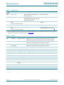
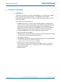
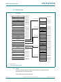
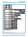
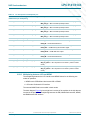
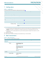
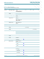
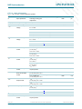
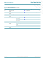
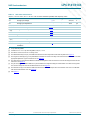
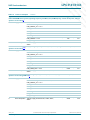
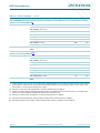
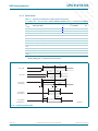
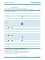
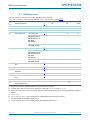
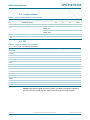
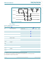
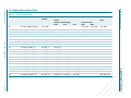
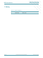
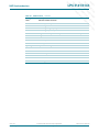
D D R R R R R D D D A A A A A FT FT FT FT FT LPC3141/3143 D R R A A FT FT FT FT A A R R D D D NXP Semiconductors D R R A FT FT FT A A R R D D D D R A F FT FT A A R R D D D FT FT A A R R D D D R A Package Name Description Version LPC3141FET180 TFBGA180 Plastic thin fine pitch ball grid array package, 180 balls, body 12 × 12 × 0.8 mm SOT570-3 LPC3143FET180 TFBGA180 Plastic thin fine pitch ball grid array package, 180 balls, body 12 × 12 × 0.8 mm SOT570-3 3.1 Ordering options Table 2. Ordering options for LPC3141/3143 Type number Core/bus Total frequency SRAM Security High-speed USB engine AES 10-bit I2S/ ADC I2 C channels LPC3141FET180 270/ 90 MHz 192 kB no Device/ Host/OTG 4 2 each yes −40 °C to +85 °C LPC3143FET180 270/ 90 MHz 192 kB yes Device/ Host/OTG 4 2 each yes −40 °C to +85 °C LPC3141_3143 Preliminary data sheet All information provided in this document is subject to legal disclaimers. Rev. 0.16 — 27 May 2010 MCI Temperature SDHC/ range SDIO/ CE-ATA © NXP B.V. 2010. All rights reserved. 2 of 74 R Ordering information Type number D Table 1. FT 3. Ordering information A Selectable boot-up: SPI flash, NAND flash, SD/MMC cards, UART, or USB On the LPC3143 only: secure booting using an AES decryption engine from SPI flash, NAND flash, SD/MMC cards, UART, or USB. DMA controller Four 32-bit timers Watchdog timer PWM module Master/slave PCM interface Random Number Generator (RNG) General Purpose I/O pins (GPIO) Flexible and versatile interrupt structure JTAG interface with boundary scan and ARM debug access Operating voltage and temperature Core voltage: 1.2 V I/O voltages: 1.8 V, 3.3 V Temperature: −40 °C to +85 °C TFBGA180 package: 12 x 12 mm, 0.8 mm pitch