1
User’s Manual
E1/E20 Emulator
Additional Document for User’s Manual
(Notes on Connection)
Supported Devices:
V850ES, V850E1
All information contained in these materials, including products and product specifications,
represents information on the product at the time of publication and is subject to change by
Renesas Electronics Corp. without notice. Please review the latest information published by
Renesas Electronics Corp. through various means, including the Renesas Electronics Corp.
website (http://www.renesas.com).
www.renesas.com
Rev.1.00
Feb 2012
Notice
1.
2.
3.
4.
5.
6.
7.
All information included in this document is current as of the date this document is issued. Such information, however, is
subject to change without any prior notice. Before purchasing or using any Renesas Electronics products listed herein, please
confirm the latest product information with a Renesas Electronics sales office. Also, please pay regular and careful attention to
additional and different information to be disclosed by Renesas Electronics such as that disclosed through our website.
Renesas Electronics does not assume any liability for infringement of patents, copyrights, or other intellectual property rights
of third parties by or arising from the use of Renesas Electronics products or technical information described in this document.
No license, express, implied or otherwise, is granted hereby under any patents, copyrights or other intellectual property rights
of Renesas Electronics or others.
You should not alter, modify, copy, or otherwise misappropriate any Renesas Electronics product, whether in whole or in part.
Descriptions of circuits, software and other related information in this document are provided only to illustrate the operation of
semiconductor products and application examples. You are fully responsible for the incorporation of these circuits, software,
and information in the design of your equipment. Renesas Electronics assumes no responsibility for any losses incurred by
you or third parties arising from the use of these circuits, software, or information.
When exporting the products or technology described in this document, you should comply with the applicable export control
laws and regulations and follow the procedures required by such laws and regulations. You should not use Renesas
Electronics products or the technology described in this document for any purpose relating to military applications or use by
the military, including but not limited to the development of weapons of mass destruction. Renesas Electronics products and
technology may not be used for or incorporated into any products or systems whose manufacture, use, or sale is prohibited
under any applicable domestic or foreign laws or regulations.
Renesas Electronics has used reasonable care in preparing the information included in this document, but Renesas Electronics
does not warrant that such information is error free. Renesas Electronics assumes no liability whatsoever for any damages
incurred by you resulting from errors in or omissions from the information included herein.
Renesas Electronics products are classified according to the following three quality grades: “Standard”, “High Quality”, and
“Specific”. The recommended applications for each Renesas Electronics product depends on the product’s quality grade, as
indicated below. You must check the quality grade of each Renesas Electronics product before using it in a particular
application. You may not use any Renesas Electronics product for any application categorized as “Specific” without the prior
written consent of Renesas Electronics. Further, you may not use any Renesas Electronics product for any application for
which it is not intended without the prior written consent of Renesas Electronics. Renesas Electronics shall not be in any way
liable for any damages or losses incurred by you or third parties arising from the use of any Renesas Electronics product for an
application categorized as “Specific” or for which the product is not intended where you have failed to obtain the prior written
consent of Renesas Electronics. The quality grade of each Renesas Electronics product is “Standard” unless otherwise
expressly specified in a Renesas Electronics data sheets or data books, etc.
“Standard”:
8.
9.
10.
11.
12.
Computers; office equipment; communications equipment; test and measurement equipment; audio and visual
equipment; home electronic appliances; machine tools; personal electronic equipment; and industrial robots.
“High Quality”: Transportation equipment (automobiles, trains, ships, etc.); traffic control systems; anti-disaster systems; anticrime systems; safety equipment; and medical equipment not specifically designed for life support.
“Specific”:
Aircraft; aerospace equipment; submersible repeaters; nuclear reactor control systems; medical equipment or
systems for life support (e.g. artificial life support devices or systems), surgical implantations, or healthcare
intervention (e.g. excision, etc.), and any other applications or purposes that pose a direct threat to human life.
You should use the Renesas Electronics products described in this document within the range specified by Renesas Electronics,
especially with respect to the maximum rating, operating supply voltage range, movement power voltage range, heat radiation
characteristics, installation and other product characteristics. Renesas Electronics shall have no liability for malfunctions or
damages arising out of the use of Renesas Electronics products beyond such specified ranges.
Although Renesas Electronics endeavors to improve the quality and reliability of its products, semiconductor products have
specific characteristics such as the occurrence of failure at a certain rate and malfunctions under certain use conditions. Further,
Renesas Electronics products are not subject to radiation resistance design. Please be sure to implement safety measures to
guard them against the possibility of physical injury, and injury or damage caused by fire in the event of the failure of a
Renesas Electronics product, such as safety design for hardware and software including but not limited to redundancy, fire
control and malfunction prevention, appropriate treatment for aging degradation or any other appropriate measures. Because
the evaluation of microcomputer software alone is very difficult, please evaluate the safety of the final products or system
manufactured by you.
Please contact a Renesas Electronics sales office for details as to environmental matters such as the environmental
compatibility of each Renesas Electronics product. Please use Renesas Electronics products in compliance with all applicable
laws and regulations that regulate the inclusion or use of controlled substances, including without limitation, the EU RoHS
Directive. Renesas Electronics assumes no liability for damages or losses occurring as a result of your noncompliance with
applicable laws and regulations.
This document may not be reproduced or duplicated, in any form, in whole or in part, without prior written consent of Renesas
Electronics.
Please contact a Renesas Electronics sales office if you have any questions regarding the information contained in this
document or Renesas Electronics products, or if you have any other inquiries.
(Note 1) “Renesas Electronics” as used in this document means Renesas Electronics Corporation and also includes its majorityowned subsidiaries.
(Note 2) “Renesas Electronics product(s)” means any product developed or manufactured by or for Renesas Electronics.
E1/E20 Emulator
Contents
Contents
1.
Outline.................................................................................................................................................................................................. 4
1.1
Features................................................................................................................................................................................................................. 4
1.2
Cautions on Using E20......................................................................................................................................................................................... 4
1.3
Configuration of Manuals .................................................................................................................................................................................... 4
2.
Designing the User System ................................................................................................................................................................. 5
2.1
Connecting the Emulator with the User System .................................................................................................................................................. 5
2.2
Pin Assignments of the Connector on the User System ...................................................................................................................................... 6
2.3
Recommended Circuit between the Connector and the MCU............................................................................................................................. 6
2.3.1
JTAG Recommended Circuit....................................................................................................................................................................7
2.3.2
UART Recommended Circuit ...................................................................................................................................................................8
2.3.3
CSI Recommended Circuit .......................................................................................................................................................................9
2.3.4
Regarding Connection of FLMD0 ......................................................................................................................................................... 10
2.3.5
Regarding Connection of RESET......................................................................................................................................................... 10
3.
Setting of Security ID and Securing of debugging resources ............................................................................................................ 13
3.1
Setting of Security ID......................................................................................................................................................................................... 13
3.2
Reset handler ...................................................................................................................................................................................................... 14
3.3
Securing of area for debugging .......................................................................................................................................................................... 15
3.4
Securing of communication serial interface ...................................................................................................................................................... 16
4.
Specifications..................................................................................................................................................................................... 18
5.
Notes on Usage ................................................................................................................................................................................. 19
5.1
Lists .................................................................................................................................................................................................................... 19
5.2
Details................................................................................................................................................................................................................. 20
R20UT1001EJ0100 Rev.1.00
Feb 01, 2012
Page 3 of 24
E1/E20 Emulator
1.
Outline
1.1
Features
Outline
E1/E20 Emulator is an on-chip debug emulator with flash programming function, which is used for debugging and programming a
program to be embedded in on-chip flash memory microcontrollers. This product can debug with the target microcontroller connected to
the target system, and can write programs to the on-chip flash memory of microcontrollers.
1.2
Cautions on Using E20
The functions used for debugging of the V850E2M, V850E2S device by using the E20 are the same as in the E1. Large trace function,
characteristic functions of the E20, cannot be used. The power supply function from the E20 is not supported.
1.3
Configuration of Manuals
Documentation for the E1/E20 emulator manual is in two parts: the E1/E20 Emulator User’s Manual and the E1/E20 Emulator
Supplementary Document for the User’s Manual (this manual). Different versions of the latter correspond to different sets of MCUs. Be
sure to read both of the manuals before using the E1/E20 emulator (hereinafter referred to as "the emulator").
(1)
(2)
The E1/E20 emulator user’s manual has the following contents:
•
Components of the emulators
•
Emulator hardware specification
•
Connection to the emulator and the host computer and user system
The E1/E20 Emulator Supplementary Document for the User’s Manual has the following contents:
•
For use in hardware design, an example of connection and the interface circuit required to connect the emulator.
•
Notes on using the emulator
R20UT1001EJ0100 Rev.1.00
Feb 01, 2012
Page 4 of 24
2.Designing the User System
2.
E1/E20 Emulator
Designing the User System
To connect the E1/E20 emulator (hereinafter referred to as the emulator), a connector for the user system interface cable must be
mounted on the user system. When designing the user system, read this section of this manual and the hardware manual for the MCUs.
2.1
Connecting the Emulator with the User System
Table 2-1 shows the type numbers of the E1/E20 emulators
Table 2-1 Type Numbers
Type
仕様
Manufacturer
Number
14-pin
7614-6002
Sumitomo 3M Limited
14-pin straight type (Japan)
Connector
2514-6002
3M Limited
14-pin straight type (other countries)
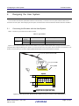
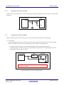
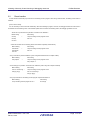
Figures 2.1 and 2.2 show examples of the connection between a user system interface cable of the 14-pin type. Do not mount other
components with a height exceeding 10 mm within 5 mm of the connector on the user system. 38-pin of the E20 is not supported. To use
the E20, use the 38-pin/14-pin conversion adapter [R0E000200CKA00] that comes with the E20 for connection.
14-pin user system interface cable
14-pin type connector
User system
Top View
5mm
2
4
6
8
10 12 14
1
3
5
7
9
11 13
5mm
5mm
5mm
Area with limit on mounted components
(heights must be no greater than 10mm)
Figure 2-1 Connecting the User System Interface Cable to the 14-pin Connector of the E1/E20 Emulator
R20UT1001EJ0100 Rev.1.00
Feb 01, 2012
Page 5 of 24
2.Designing the User System
2.2
E1/E20 Emulator
Pin Assignments of the Connector on the User System
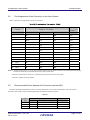
Table 2-2 shows the pin assignments of the 14-pin connectors.
Table 2-2 Pin assignments of the connector (14-pin)
Pin No.
Input/
Signal (#:Low Active)
JTAG Connection
Outputnote3
CSI Connection
UART Connection
TCK
-
SCK
入力
GND
GND
GND
-
3
TRST#
CLK
CLK
入力
4
FLMD0
FLMD0
FLMD0
入力
5
TDO
RxD
SI
出力
6
-
RESET_IN#
RESET_IN#
出力
7
TDI
TxD
SO
入力
8
VDD
VDD
VDD
-
9
TMS
FLMD1
FLMD1
入力
10
-
RESET_OUT#
11
-
-
HS
出力
GND
GND
GND
-
RESET_OUT#
RESET_OUT#
GND
GND
1
2
12
【注1】
【注1】
13
14
Notes 1.
【注1】
【注2】 RESET_OUT#
【注2】 RESET_OUT#
【注2】
【注2】
GND
入力
入力
-
Securely connect pins 2, 12, and 14 of the connector to GND of the user system. These pins are used for electrical grounding
as well as for monitoring of connection with the user system by the E1/E20.
2. Securely connect both pin 10 and pin 13. These pins are also used to monitor the user system.
3. Input to or output from the user system
2.3
Recommended Circuit between the Connector and the MCU
This section describes recommended circuits for connection between the 14-pin connector and the MCU. There are 3 types of
connection JTAG, UART and CSI as following table. Select the relevant circuit for the purpose.
Table 2-3
Interface
Debugging
Programming
Type
Support
User space for debugging
Support
JTAG
○
None
×
UART
○
ROM:2K bytes, RAM:16 bytes
○
CSI
○
ROM:2K bytes, RAM:16 bytes
○
R20UT1001EJ0100 Rev.1.00
Feb 01, 2012
Page 6 of 24
2.Designing the User System
2.3.1
E1/E20 Emulator
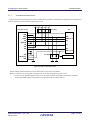
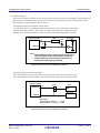
JTAG Recommended Circuit
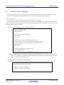
Figure 2-2 shows a recommended circuit for JTAG connection. Be sure to take into consideration the specifications of the target device
as well as measures to prevent noise when designing your circuit.
EVDD
EVDD
EVDD
EVDD
EVDD
14-pin type connector
TCK
GND
TRST
FLMD0
TDO
RESET_IN
TDI
VDD
TMS
GND
RESET_OUT
GND
MCU
1K~10KΩ
1
DCK
2
3
DRST
4
FLMD0 【Note1】
5
DDO
6
7
DDI
8
9
DMS
10
RESET 【Note2】
11
12
1K~10KΩ
13
Reset Circuit 【Note2】
14
Figure 2-2 JTAG recommended circuit
【Caution】Wiring patterns between the connector and the MCU must be as short as possible
【Note】1. This circuit is for not using flash self programming. To use flash self programming, refer to 2.3.4.
2. This circuit is for reset MCU between turning on the user system to startup the debugger, and this circuit is designed
assuming that RESET signal is output from the N-ch open-drain buffer. For details, refer to 0.
R20UT1001EJ0100 Rev.1.00
Feb 01, 2012
Page 7 of 24
2.Designing the User System
2.3.2
E1/E20 Emulator
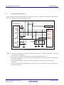
UART Recommended Circuit
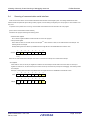
Figure 2-3 shows a recommended circuit for UART connection. Be sure to take into consideration the specifications of the target device
as well as measures to prevent noise when designing your circuit.
EVDD
GND
【Note1】 CLK
FLMD0
RxD
RESET_IN
TxD
VDD
FLMD1
RESET_OUT
GND
RESET_OUT
GND
EVDD
3K~
10KΩ
14-pin type connector
-
EVDD
1K
1
Reset Circuit 【Note5】
2
MCU
3
4
FLMD0【Note2】
5
TxD 【Note3】
6
7
RxD 【Note3】
8
10K
9
FLMD1【Note4】
10
RESET【Note5】
11
12
1K~10KΩ
13
14
Figure 2-3 UART recommended circuit
【Note】1. This pin may be used to supply an external clock during flash programming (4, 8 or 16 MHz). For the connection, refer to the
user's manual for the target device.
2. This circuit is for not using flash self programming. To use flash self programming, refer to 2.3.4.
3. Read the serial interface pin names on the target device side as those for flash programming supported by the target device
(For example, TxD0/RxD0).
4. In case the alternate function of this pin is used, connect to FLMD1 pin. The emulator output low level when flash
programming.
5. This circuit is designed assuming that RESET signal is output from the N-ch open-drain buffer (out put resistance: 100Ω or
less). For details, refer to 0.
R20UT1001EJ0100 Rev.1.00
Feb 01, 2012
Page 8 of 24
2.Designing the User System
2.3.3
E1/E20 Emulator
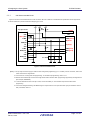
CSI Recommended Circuit
Figure 2-4 shows a recommended circuit for CSI connection. Be sure to take into consideration the specifications of the target device
as well as measures to prevent noise when designing your circuit.
EVDD
GND
【Note1】 CLK
FLMD0
SI
RESET_IN
SO
VDD
FLMD1
RESET_OUT
HS
GND
RESET_OUT
GND
EVDD
3K~
10KΩ
14-pin type connector
SCK
EVDD
1K
Reset Circuit 【Note5】
1
2
MCU
3
SCK
4
FLMD0 【Note2】
5
SO 【Note3】
6
7
SI 【Note3】
8
10K
9
FLMD1 【Note4】
10
RESET 【Note5】
11
HS
12
13
1K~10KΩ
14
Figure 2-4 CSI recommended circuit
【Note】1. This pin may be used to supply an external clock during flash programming (4, 8 or 16 MHz). For the connection, refer to the
user's manual for the target device.
2. This circuit is for not using flash self programming. To use flash self programming, refer to 2.3.4.
3. Read the serial interface pin names on the target device side as those for flash programming supported by the target device
(For example, SOB0/SIB0).
4. In case the alternate function of this pin is used, connect to FLMD1 pin. The emulator output low level when flash
programming.
5. This circuit is designed assuming that RESET signal is output from the N-ch open-drain buffer (out put resistance: 100Ω or
less). For details, refer to 0.
R20UT1001EJ0100 Rev.1.00
Feb 01, 2012
Page 9 of 24
2.Designing the User System
2.3.4
E1/E20 Emulator
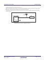
Regarding Connection of FLMD0
FLMD0 is used to write the flash memory. In case the user program use flash self programming, connect as Figure 2-5. PortX indicates
arbitrary Port.
Connector for Emulator
MCU
FLMD0
FLMD0
10kΩ
100Ω
Port X
Figure 2-5 Recommended circuit when using flash self programming
2.3.5
Regarding Connection of RESET
RESET connection depends on each interface type, JTAG, UART or CSI. Refer to following due to the interface type.
(1)
JTAG interface
Connect the RESET signal as shown in Figure 2-6 if any of the conditions listed below is satisfied. When none of the following
conditions are satisfied, leave open the pin for the RESET signal that is output from the E1/E20 emulator.
・ The target device should be kept in the reset state before debugger startup or after debugger termination.
・ The JTAG signal pins are alternate-function pins in the specifications of the target device, and OCDM register is set to use
port/peripheral function pin at the user program.
Connector for Emulator
RESET_OUT
13
MCU
_RESET
Reset Circuit
EVDD
EVDD
The output from the reset circuit must be N-ch open-drain output or signal generated
using only resister and capacitor.
Figure 2-6 Reset circuit in case of JTAG connection
R20UT1001EJ0100 Rev.1.00
Feb 01, 2012
Page 10 of 24
2.Designing the User System
(2)
E1/E20 Emulator
UART/CSI Interface
Select one of the following 3 methods and connect the reset signal in the circuit. During on-chip debugging, a reset signal from the
target system is input to E1/E20 Emulator, masked, and then output to the target device. Therefore, the reset signal connection
varies depending on whether E1/E20 emulator is connected.
●Automatically switching the reset signal via series resistor
This connection in Figure 2-7 is designed assuming that the reset circuit on the target system contains an N-ch
open-drain buffer (output resistance: 100Ω or less). The VDD or GND level may be unstable when the logic
of RESET_IN/OUT of E1/E20 Emulator is inverted, so observe the conditions described below in Remark.
Connector for Emulator
RESET_OUT
MCU
10, 13
_RESET
R1
RESET_IN
Reset Circuit
EVDD
EVDD
R2
6
Remark: Make the resistance of at least R1 ten times that of R2, R1 being 10 kΩ or
more. Pull-up resistor R2 is not required if the buffer of the reset circuit
consists of CMOS output. The circuit enclosed by a dashed line is not
required when only flash programming is performed.
Figure 2-7 Reset circuit in case of UART/CSI connection 1
●Manually switching the reset signal with jumper
Figure 2-8 illustrates the circuit connection for the case where the reset signal is switched using the jumper,
with or without E1/E20 emulator connected. This connection is simple, but the jumper must be set manually.
Connector for Emulator
RESET_OUT
10, 13
Jumper
1
MCU
_RESET
2
3
Reset Circuit
RESET_IN
6
Jumper Setting
When E1 Emulator is connected
: 1-2 short
When E1 Emulator is not connected : 2-3 short
Figure 2-8 Reset circuit in case of UART/CSI connection 2
R20UT1001EJ0100 Rev.1.00
Feb 01, 2012
Page 11 of 24
2.Designing the User System
E1/E20 Emulator
●Resetting the target device by power-on clear (POC) only
Figure 2-9 illustrates the circuit connection for the case where the target device is only reset via POC without using the reset pin.
RESET_OUT is valid only when the debugger is running or during flash programming.
The operation is not guaranteed if the power to the target system is shut down during debugging. Note that the POC function
cannot be emulated.
EVDD
1k~10kΩ
Connector for Emulator
10, 13
RESET_OUT
MCU
_RESET
RESET_IN
Figure 2-9 Reset circuit in case of UART/CSI connection 3
R20UT1001EJ0100 Rev.1.00
Feb 01, 2012
Page 12 of 24
3.Setting of Security ID and Securing of debugging resources
3.
E1/E20 Emulator
Setting of Security ID and Securing of debugging resources
The user must prepare the following to perform communication between E1/E20 emulator and the target device and implement each
debug function. Refer to the descriptions on the following sections and set these items in the user program or using the compiler options.
When using JTAG interface, the setting of this section is needless.
3.1
Setting of Security ID
This setting is required to prevent the memory from being read by an unauthorized person. Embed a security ID at addresses 0x70 to
0x79 in the internal flash memory. The debugger starts only when the security ID that is set during debugger startup and the security ID
set at addresses 0x70 to 0x79 match. If bit 7 of address 0x79 is ″0″, however, debugging is disabled. In such a case, there are no
methods to start the debugger. Debugging is mainly disabled for mass-produced devices.
If the user has forgotten the security ID or to enable debugging, erase the flash memory and set the security ID again.
[How to set security ID]
Embed a security ID at addresses 0x70 to 0x79 in the user program.
If the security ID is embedded as follows, for example, the security ID set by the debugger is ″123456789ABCDEF123D4″ (not
case-sensitive).
R20UT1001EJ0100 Rev.1.00
Feb 01, 2012
Address
Value
0x70
0x12
0x71
0x34
0x72
0x56
0x73
0x78
0x74
0x9A
0x75
0xBC
0x76
0xDE
0x77
0xF1
0x78
0x23
0x79
0xD4
Page 13 of 24
3.Setting of Security ID and Securing of debugging resources
3.2
E1/E20 Emulator
Reset handler
A reset handler includes the jump instruction for the debug monitor program. When using JTAG interface, the setting of this section is
needless.
[How to secure areas]
It is not necessary to secure this area intentionally. When downloading a program, however, the debugger rewrites the reset vector in
accordance with the following cases. If the rewritten pattern does not match the following cases, the debugger generates an error.
•When two nop instructions are placed in succession from address 0
Before writing
0x0 nop
After writing
→
0x2 nop
Jumps to debug monitor program at 0x0
0x4 xxxx
0x4 xxxx
• When two 0xFFFF are successively placed from address 0 (already erased device)
Before writing
0x0 0xFFFF
After writing
→
0x2 0xFFFF
Jumps to debug monitor program at 0x0
0x4 xxxx
0x4 xxxx
• The jr instruction is placed at address 0 (when using Renesas Electronics compiler CA850)
Before writing
0x0 jr disp22
After writing
→
Jumps to debug monitor program at 0x0
0x4 jr disp22 – 4
• mov32 and jmp are placed in succession from address 0 (when using IAR compiler ICCV850)
Before writing
After writing
0x0 mov imm32,reg1 →
Jumps to debug monitor program at 0x0
0x6 jmp [reg1]
0x4 mov imm32,reg1
0xa jmp [reg1]
• The jump instruction for the debug monitor program is placed at address 0
Before writing
After writing
Jumps to debug monitor program at 0x0 →
No change
R20UT1001EJ0100 Rev.1.00
Feb 01, 2012
Page 14 of 24
3.Setting of Security ID and Securing of debugging resources
3.3
E1/E20 Emulator
Securing of area for debugging
The area for debugging is for performing initialization processing for debug communication interface and RUN or break processing
for the CPU. The internal ROM area must be filled with 0xFF. This area must not be rewritten by the user program.
[How to secure areas]
It is not necessarily required to secure this area if the user program does not use this area.
To avoid problems that may occur during the debugger startup, however, it is recommended to secure this area in advance, using the
compiler. The following shows examples for securing the area, using the Renesas Electronics compiler CA850. Add the assemble source
file and link directive code, as shown below.
・Assemble source (Add the following code as an assemble source file.)
-- Secures 2 KB space for monitor ROM section
.section "MonitorROM", const
.space 0x800, 0xff
Note
-- Secures interrupt vector for debugging
.section "DBG0"
.space 4, 0xff
-- Secures interrupt vector for serial communication for receive
-- Secures vector for receive error interrupt and receive status interrupt, if any
-- Change the section name according to serial communication mode used
.section "INTCSI00"
.space 4, 0xff
-- Secures 16 byte space for monitor ROM section
.section "MonitorRAM", bss
.lcomm monitorramsym, 16, 4 /* defines monitorramsym symbol */
Note The downloading speed can be increased by replacing this line with the statement “monitorromsym:” to perform a symbol
definition only. This effect is not applicable if values are filled into a hole (area without a code). When performing filling, the
filling value must be 0xFF for securing the area.
・Link directive (Add the following code to the link directive file.)
The following shows an example when the internal ROM end address is 0x3ffff and internal RAM end address is 0x3ffefff.
MROMSEG : !LOAD ?R V0x03f800{
MonitorROM = $PROGBITS ?A MonitorROM;
};
MRAMSEG : !LOAD ?RW V0x03ffeff0{
MonitorRAM = $NOBITS ?AW MonitorRAM;
};
R20UT1001EJ0100 Rev.1.00
Feb 01, 2012
Page 15 of 24
3.Setting of Security ID and Securing of debugging resources
3.4
E1/E20 Emulator
Securing of communication serial interface
UART or CSI-H/S is used for communication between E1/E20 emulator and the target system. The settings related to the serial
interface modes are performed by the debug monitor program, but if the setting is changed by the user program, a communication error
may occur.
To prevent such a problem from occurring, communication serial interface must be secured in the user program.
[How to secure communication serial interface]
Create the user program observing the following points.
• Serial interface registers
Do not set the registers related to UART and CSI-H/S in the user program.
• Interrupt mask register
When UART is used, do not mask receive end interrupts
Note
. When CSI-H/S is used, do not mask transmit end interrupts. The
following shows an example.
Example Setting other than below is prohibited when the target device is the V850ES/KJ2 and CSI00 is used.
CSI0IC0
7
6
5
4
3
2
1
0
x
0
x
x
x
x
x
x
x:Any
Note: Do not mask receive these interrupts when there is a receive error interrupt or a receive status interrupt.
• Port registers
When UART is used, do not set port registers to make the TxD and RxD pins invalid. When CSI-H/S is used, do not set port
registers to make the SI, SO, SCK and H/S pins invalid. The H/S pin is used as the port output for debugging. The following shows
two examples.
Example 1: Setting other than below is prohibited when the target device is the V850ES/KJ2 and UART0 is used.
PFC3
PMC3L
7
6
5
4
3
2
1
0
x
x
x
x
x
x
0
0
7
6
5
4
3
2
1
0
x
x
x
x
x
x
1
1
x: Any
R20UT1001EJ0100 Rev.1.00
Feb 01, 2012
Page 16 of 24
3.Setting of Security ID and Securing of debugging resources
E1/E20 Emulator
Example 2: Setting other than below is prohibited when the target device is the V850ES/HG2 and CSIB0 is used.
PMC4
PMCCM
PMCM
PCM
7
6
5
4
3
2
1
0
x
x
x
x
x
1
1
1
7
6
5
4
3
2
1
0
x
x
x
x
x
x
x
0
7
6
5
4
3
2
1
0
x
x
x
x
x
x
x
0
7
6
5
4
3
2
1
x
x
x
x
x
x
x
0
Note
Read-only
x: Any
Note: The port values corresponding to the H/S pin are changed by the monitor program according to the debugger status. To perform
port register settings in 8-bit units, usually the user program can use read-modify-write. If an interrupt for debugging occurs
before writing, however, an unexpected operation may be performed.
R20UT1001EJ0100 Rev.1.00
Feb 01, 2012
Page 17 of 24
4.Specifications
4.
E1/E20 Emulator
Specifications
Specifications are below table.
Large Item
Middle Item
Hardware
Common
Target host machine
Related
debugging
Small Item
Specification
Computer equipped with a USB port
OS is due to the software tool.
User system interface
14-pin connector
Host machine interface
USB2.0 (Full speed/ High speed)
Connection to the user system
Connection by the provided user-system interface
cable
Power supply function (E1 Emulator used)
3.3V or 5.0V, set in software tool, can be supplied to
the user system (with current up to 200 mA)
Power supply for the emulator
No need (the host computer supplies power through
the USB)
Break
Event
Software break
RAM area :2000 points
Hardware break
2points (commonly used by execution and access)
Forced break
Available
Number of events
2points (commonly used by execution and access)
Available function
Only hardware break
Combination of events
OR, sequential
Measurement item
From run to break
Performance
JTAG interface
Trace
Performance measurement
ROM area :4 points
Unavailable
Resolution 100ns, Max. measurement time 3.5
minutes (During DCK is 20MHz)
UART/CSI interface
Resolution 100us, Max. measurement time 100
hour
Related
programming
Realtime RAM monitor
Available (CPU is used when monitoring)
Direct memory modification
Available (CPU is used when monitoring)
Debugging console
Unavailable
Downloading to external flash memory
Available (Depends on Software)
Hot plug-in
Unavailable
Security
10-byte ID code authentication
Clock supply
16, 8, or 4 MHz clock can be supplied
Clock mounted on the target system can be used
Security flag setting
Available
Standalone operation
Unavailable (must be connected to host machine)
R20UT1001EJ0100 Rev.1.00
Feb 01, 2012
Page 18 of 24
5.Notes on Usage
5.
E1/E20 Emulator
Notes on Usage
Make sure to notes on usage in this section.
5.1
Lists
Table 5-1 Lists of notes on usage
No
Item
Target
1
Handling of device that was used for debugging
JTAG, UART, CSI
2
Alternate functions
JTAG, UART, CSI
3
Notes on downloading
JTAG, UART, CSI
4
Regarding ROM correction function
JTAG, UART, CSI
5
Regarding current consumption
JTAG, UART, CSI
6
Regarding standby release with debugging functions
JTAG, UART, CSI
7
Notes on flash self programming
JTAG, UART, CSI
8
Regarding POC function and emulation of turning OFF
JTAG, UART, CSI
9
Regarding I/O buffer when using reset mask
JTAG
10
When forced break, RRM function and DMM function do not operate
UART, CSI
11
Writing to peripheral I/O registers that requires a specific sequence, using DMM function
UART, CSI
12
Writing quality of flash programming
UART, CSI
13
Debugging with real machine running
UART, CSI
14
Regarding watchdog timer
UART, CSI
15
Regarding external reset
UART, CSI
16
Regarding reset vector handling
UART, CSI
R20UT1001EJ0100 Rev.1.00
Feb 01, 2012
Page 19 of 24
5.Notes on Usage
5.2
E1/E20 Emulator
Details
No.1 Handling of device that was used for debugging
Target: JTAG, UART, CSI
Description: Do not mount a device that was used for debugging on a mass-produced product, because the flash memory was rewritten
during debugging and the number of rewrites of the flash memory cannot be guaranteed. When the flash memory can not
be rewritten, the software tool generates the error. In case of that, change the mounted device.
No.2
Alternate functions
Target: JTAG, UART, CSI
Description: The alternate functions of these pins cannot be used during on-chip debugging. And be careful not to conflict the signals
from emulator while the flash programming is operating.
No.3
Notes on downloading
Target: JTAG, UART, CSI
Description: When debugging, reset CPU before downloading. If DMA transfer to the internal RAM is performed while a program is
being downloaded to the flash memory, downloading of the program may not be performed normally.
No.4
Regarding ROM correction function
Target: JTAG, UART, CSI
Description: Do not use the ROM correction function or else unexpected breaks will occur.
No.5
Regarding current consumption
Target: JTAG, UART, CSI
Description: The current consumption in the target device increases during debugging compared with that in normal operation mode,
because the OCD unit of the target device operates during debugging.
No.6
Regarding standby release with debugging functions
Target: JTAG, UART, CSI
Description: In case using the RRM function and DMM function, the standby mode is released when the memory is read or written.
No.7
Notes on flash self programming
Target: JTAG, UART, CSI
Description: Do not break in ROM area during flash environment. In case of monitoring memory with RRM function, a temporary break
is executed. So do not use RRM function when using flash self programming.
Do not modify the debug monitor area when using UART/CSI interface.
No.8
Regarding POC function and emulation of turning OFF
Target: JTAG, UART, CSI
Description: Make sure that the power to the target system is not shut down during debugging. Regarding to check the operation of
POC function and tuning OFF, perform without the emulator. In case the user system is turning OFF instantaneously, the
debugger may hang up.
R20UT1001EJ0100 Rev.1.00
Feb 01, 2012
Page 20 of 24
5.Notes on Usage
No.9
E1/E20 Emulator
Regarding I/O buffer when using reset mask
Target: JTAG
Description: The I/O buffer (port pin) may enter the reset status depending on the target device when a reset is input from the pin, even
if reset is masked by the mask function.
No.10
When forced break, RRM function and DMM function do not operate
Target: UART, CSI
Description: Forced breaks, RRM function and DMM function cannot be executed if one of the following conditions is satisfied.
・Interrupts are disabled (DI)
・Interrupts issued for UART/CSI interface are masked
・Standby mode is entered while standby release by a maskable interrupt is prohibited
・When using UART interface, the main clock has been stopped
・When using UART interface, a clock different from the one specified in the debugger is used for communication
No.11
Writing to peripheral I/O registers that requires a specific sequence, using DMM function
Target: UART, CSI
Description: Peripheral I/O registers that requires a specific sequence cannot be written with the DMM function.
No.12
Writing quality of flash programming
Target: UART, CSI
Description: To improve the writing quality, fully understand, verify, and evaluate the following items before using E1/E20 emulator.
・Circuits are designed as described in the user's manuals for the device and E1/E20 emulator.
・The device, E1/E20 emulator and the software are used as described in each user's manual.
・The power supplied to the target system is stable.
No.13
Debugging with real machine running
Target: UART, CSI
Description: If debugging is performed with a real machine running, without using emulator, write the user program using the
programming software. Programs downloaded by the debugger include the monitor program, and such a program
malfunctions if it is not controlled via E1/E20 emulator.
No.14
Regarding watchdog timer
Target: UART, CSI
Description: The watchdog timer is forcibly stopped by the debug monitor program. Therefore, do not use the option byte to specify that
the watchdog timer cannot be stopped. For details about the option byte settings, see the user’s manual of the target
device.
No.15
Regarding external reset
Target: UART, CSI
Description: A break occurs when an external reset occurs (except when resets are masked) or an internal reset occurs.
No.16
Regarding reset vector handling
Target: UART, CSI
Description: Reset vector handling is not supported.
R20UT1001EJ0100 Rev.1.00
Feb 01, 2012
Page 21 of 24
E1/E20 Emulator
Additional Document for User's Manual (Notes on Connection)
Publication Date:
Feb 01, 2012
Rev.1.00
Published by:
Renesas Electronics Corporation
http://www.renesas.com
SALES OFFICES
Refer to "http://www.renesas.com/" for the latest and detailed information.
Renesas Electronics America Inc.
2880 Scott Boulevard Santa Clara, CA 95050-2554, U.S.A.
Tel: +1-408-588-6000, Fax: +1-408-588-6130
Renesas Electronics Canada Limited
1101 Nicholson Road, Newmarket, Ontario L3Y 9C3, Canada
Tel: +1-905-898-5441, Fax: +1-905-898-3220
Renesas Electronics Europe Limited
Dukes Meadow, Millboard Road, Bourne End, Buckinghamshire, SL8 5FH, U.K
Tel: +44-1628-585-100, Fax: +44-1628-585-900
Renesas Electronics Europe GmbH
Arcadiastrasse 10, 40472 Düsseldorf, Germany
Tel: +49-211-65030, Fax: +49-211-6503-1327
Renesas Electronics (China) Co., Ltd.
7th Floor, Quantum Plaza, No.27 ZhiChunLu Haidian District, Beijing 100083, P.R.China
Tel: +86-10-8235-1155, Fax: +86-10-8235-7679
Renesas Electronics (Shanghai) Co., Ltd.
Unit 204, 205, AZIA Center, No.1233 Lujiazui Ring Rd., Pudong District, Shanghai 200120, China
Tel: +86-21-5877-1818, Fax: +86-21-6887-7858 / -7898
Renesas Electronics Hong Kong Limited
Unit 1601-1613, 16/F., Tower 2, Grand Century Place, 193 Prince Edward Road West, Mongkok, Kowloon, Hong Kong
Tel: +852-2886-9318, Fax: +852 2886-9022/9044
Renesas Electronics Taiwan Co., Ltd.
13F, No. 363, Fu Shing North Road, Taipei, Taiwan
Tel: +886-2-8175-9600, Fax: +886 2-8175-9670
Renesas Electronics Singapore Pte. Ltd.
1 harbourFront Avenue, #06-10, keppel Bay Tower, Singapore 098632
Tel: +65-6213-0200, Fax: +65-6278-8001
Renesas Electronics Malaysia Sdn.Bhd.
Unit 906, Block B, Menara Amcorp, Amcorp Trade Centre, No. 18, Jln Persiaran Barat, 46050 Petaling Jaya, Selangor Darul Ehsan, Malaysia
Tel: +60-3-7955-9390, Fax: +60-3-7955-9510
Renesas Electronics Korea Co., Ltd.
11F., Samik Lavied' or Bldg., 720-2 Yeoksam-Dong, Kangnam-Ku, Seoul 135-080, Korea
Tel: +82-2-558-3737, Fax: +82-2-558-5141
© 2012 Renesas Electronics Corporation. All rights reserved.
Colophon 1.1
E1/E20 Emulator
Additional Document for User’s Manual
(Notes on Connection)