1
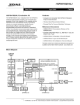
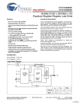
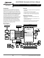
ISL5217EVAL1 Evaluation Kit User’s Manual
TM
Application Note
PRELIMINARY
June 2001
AN9910.1
Introduction
Features
The ISL5217EVAL1 is an evaluation kit for the ISL5217
Quad Programmable Upconverter. The kit consists of an
evaluation Circuit Card Assembly (CCA) complete with the
ISL5217 device and additional circuitry to provide for control
via a computer parallel port. Windows based demonstration
software is provided for full user programmability and control
of all ISL5217 operational modes. The evaluation board
provides digital outputs which are accessible through
standard logic analyzer headers. It also provides both single
ended and differential analog outputs via SMA connectors
and Low Voltage Differential Signals (LVDS) outputs.
Documentation includes a user’s manual, full evaluation
board schematics and PCB layout materials. Special filter
files, pattern files and example configuration script files are
included for quickly configuring the board.
• Evaluation CCA complete with ISL5217 Programmable
Upconverter
1
• Example Files For Common Modulation Techniques
• Parallel Port Ribbon Cable and Power Supply Cable
Reference Documents
• ISL5217EVAL1 CCA Demonstration Software in File
ISL5217.exe
• Example Configuration Files in *.js, Filter Files in *.coe,
and Pattern Files in *.pat
• ISL5217EVAL1 Schematics in File sch217eval1.pdf
• ISL5217EVAL1 Layout in File fab217eval1.pdf
J2 QIN<19:0>
J9-JTAG/MISC
J1 IIN<19:0>
J5-P<15:0>
CAS-IN-CLK
SYNCO
DATA /16
CONTROL /9
SERIAL CHANNEL A /5
SERIAL CHANNEL B /5
SERIAL CHANNEL C /5
J6-SERIAL C/D
ADDRESS /7
J7-SERIAL A/B
[ /Title
(AN99
10)
/Subjec
t
(ISL52
17EVA
L1
Evalua
tion
Block Diagram
Kit
User’s
COMPUTER PARALLEL PORT
J10-COMP. INTFC
Manua
l)
/17
/Autho
r ()
/Keyw
U4
LVX161284
ords
IEEE XCVR
(Intersi
/17
U3
l
XCV150-4PQ240C
FPGA
Corpor
U10
/11
XC9572XL
ation,
CPLD
semico
/4
nducto
DATA /32
U5
HC244
CONTROL /4
r, ,
BUFFER
ADDRESS /20
Progra
mmabl
e
Upcon
verter,
3.3V
U12
Digital
5.0V
REG
Up
2.5V
U13
J16
Conver
REG
VIN
ter,
Interpo
lation,
Baseba
nd to
• Windows-Based Demonstration Software
SERIAL CHANNEL D /5
IIN<19:0> QIN<19:0>
U1
ISL5217
PROG. UP CONVERTER
P<15:0>
A<6:0>
RDMODE, OFFBIN, OUTEN<1:0>, WR
RD, CS, RST, TRITST
SDA, TXENA, UPDA, SCKLA, FSRA
SDB, TXENB, UPDB, SCKLB, FSRB
EXTERNAL CLK
U6
OSC
J11
SMA
U7
CY7B9111V
CLOCK BUF.
SDC, TXENC, UPDC, SCKLC, FSRC
SDD, TXEND, UPDD, SCKLD, FSRD
U2
CY7C1339
SRAM
CLK
TO DEVICE CLKS
J8-CONTROL
J14
SMA
QOUT
IOUT<19:0> QOUT<19:0>
J17-FPGA DEBUG
U8
DS90CR217
LVDS
U9
DS90CR217
LVDS
J12
IOUT
J13
QOUT
CAS-SYNCO
CAS-OUT-CLK
U11
HI5828
DAC
J15
SMA
IOUT
J3 IOUT<19:0>
J4 QOUT<19:0>
CAUTION: These devices are sensitive to electrostatic discharge; follow proper IC Handling Procedures.
1-888-INTERSIL or 321-724-7143 | Intersil and Design is a trademark of Intersil Americas Inc.
Copyright © Intersil Americas Inc. 2001, All Rights Reserved
Application Note 9910
Getting Started
Installation Requirements
1. A personal computer running Windows 95, Windows 98,
or Windows NT with a bidirectional parallel port.
2. A 5VDC power supply capable of supporting the
evaluation CCA by sourcing 2.0A.
Software Installation
Windows 95
1. Execute the ‘ISL5217.exe’ installation program from the
distribution media. This program will create folder
ISL5217 and install the required files.
2. Select and execute ‘ste51en.exe.’ This program will install
the required Windows scripting host.
Windows 98
1. Execute the ‘ISL5217.exe’ installation program from the
distribution media. This program will create folder
ISL5217 and install the required files.
2. If the target computer’s operating system was loaded with
the default system configuration, it is not necessary to
select and execute “ste51en.exe.” This program would
have been part of the default. If scripting errors are
encountered, execute ‘ste51en.exe.’
Windows NT/Windows 2000
1. Execute the ‘ISL5217.exe’ installation program from the
distribution media. This program will create folder
ISL5217 and install the required files.
2. Select and execute ‘ste51en.exe.’ This program will install
the required Windows scripting host.
3. Execute ‘Port95nt.exe’ from the disk. ‘Port95nt.exe’
installs the DriverLINX Port I/O Driver parallel port
drivers, a necessary component for running the software
under Windows NT/2000. In order to run ‘Port95nt.exe’
successfully you must have administrator privileges on
your NT machine. Upon completion, you must reboot in
order for the driver to take effect.
Hardware Description
Board Components
The evaluation board consists of four major components as
depicted in the block diagram:
1. ISL5217 U1: This is the Quad Programmable Upconverter
device. This device is clocked by a user selectable
BIT-CLK or by the onboard programmable skew clock
buffer U7’s CLK2.
2. RAM U2. The board uses a 128K x 32 bits synchronouspipelined cache RAM to store digital data patterns for the
In-phase and Quadrature inputs to the ISL5217. The
RAM is clocked with U7’s CLK1. The RAM device
memory is partitioned to allocate separate serial channel
A-D input areas for the ISL5217. Space is also reserved
to provide for dynamic reconfiguration data storage to
allow real time re-configuration of the ISL5217. The RAM
2
can hold I/Q stimulus patterns that are repeatable with no
overhead.
3. CPLD U10: The CPLD’s main function is serve as the
configuration handler between the PC’s parallel port and
the FPGA. The CPLD is factory configured with file
CPLD_217.jed via either the JTAG pins or the parallel
port to support loading the FPGA in selectMAP mode.
Upon initilization of the PUC.exe software, the PC begins
streaming the ISL5217.bit FPGA configuration file
information over the parallel port to the CPDL. The CPLD
bit reverses the data and manages the handshaking and
dataflow into the FPGA until configuration is complete.
Upon the FPGA’s assertion of DONE, the CPLD
three-states and allows direct parallel port access to the
FPGA to begin PUC controlled program execution. The
CPLD and FPGA are in system re-programmable,
allowing for CCA configuration fielded upgrades.
4. FPGA U3: The FPGA is the primary controller on the
CCA. It manages all input pins to the ISL5217 and
controls the RAM interface to provide for I and Q data
input into the ISL5217. It interfaces directly over the
parallel port to allow writing and readback of the ISL5217
configuration registers. The FPGA is configured upon
program initilization, which provides for fielded upgrades.
Communication with the PC is achieved using the ‘EPP’
(Standard Parallel Port) handshake. The evaluation board’s
main oscillator U6 can be removed, allowing for external
clocking through SMA connector J11. When providing this
clock externally, a 50Ω terminator for the external clock
source should be enabled through jumper JP6 1-2.
FPGA Registers
The FPGA is configured with 128 registers which contain the
control information for the CCA. The Address register and a
Data register for implementing the EPP handshake, do not
necessarily require an EPP, as the evaluation software will
emulate it. These registers can be accessed from the
evaluation software using the console commands “read” and
“write” or the script commands “PUC.read” and “PUC.write.”
For more details refer to the ‘Software Description’ section.
Hardware Configuration
Verify the following default jumper configurations per Table
1:
1. JP3, JP4, JP5, JP6 and JP7 in 2-3 position.
2. JP9 in 1-2 position.
3. J9-13 to J9-14 jumper installed.
4. JP10-JP13 in position 1-2. This configures the initial
board address to 0000.
5. JP1-JP2, JP8 not installed.
6. Connect the 5 volt power supply to the evaluation board
connector J16 utilizing the supplied power cable. Ensure
the power supply can source 2.0A regulated at
5VDC ±5%.
Application Note 9910
WARNING: Ensure care is utilized to prevent the
application of reverse polarity power to the CCA.
7. Connect the supplied ribbon cable from the PC’s parallel
port to the evaluation board’s J10 connector ensuring the
arrow indicating pin one on the ribbon cable connector J1
and the CCA J10-1 are correctly mated.
Software Description
The evaluation software provides a graphical user interface
that allows full control over the ISL5217 evaluation board.
Through the software, all operational modes of the ISL5217
can be exerted, via the FPGA and SRAM. The software also
implements functions for loading stimulus patterns into
external memory, loading coefficient files for the internal FIR
filters, and loading gain profiles for the internal Gain Control.
The software supports user firmware development by
copying device RAM coefficients into *.hex files while
loading. This provides the user with the ability to quickly
review coefficient address allocation within the device.
Controlling the board can be done by using the forms
provided in the software, by using the active command
window to execute commands pertaining to accessing
registers directly in a peek/poke manner, or by running
scripts. The software contains eight forms, each controlling a
specific part of the board. For example, the inputs form
controls the data input mode, the time slot counters, the
serial word length, and serial modes for the device. The
software has pull-down menus through which the user can
execute various commands. These commands include
running scripts, recording macros, issuing resets, …etc.
These functions are discussed in more details in the
following sections. The software also support the control of
up to four ISL5217 boards simultaneously, through selection
of the Brd0-Brd3 indicator buttons.
NOTE: Utilize care to ensure that the Brd1-Brd3 controls
are not accessed when these boards are not present.
The software will require the selection of Actions, FPGA
Hard Reset, in the event of access to unconnected
boards.
Running the Software
1. Turn on the power supply.
2. Execute ‘PUC.exe’.
3. Select ‘File’ then ‘Load Configuration’.
4. Select the desired configuration file, then select OK.
5. The ‘PUC.exe’ active window will display the execution
results of the selected configuration and the evaluation
CCA will be operational.
Controlling the ISL5217
Software Forms
The software provides six different forms for controlling the
ISL5217 device, one form for controlling the evaluation CCA,
and one form controlling the factory test modes of the
3
ISL5217 device. These forms can set or clear various
register bits, and load associated memories. For more
information concerning the interpretations of the bit fields
inside these forms, refer to the ISL5217 data sheet.
Switching between forms can be done using the Tab toolbar.
A brief discussion of the software forms follows:
Many of the forms contain Channel 0-Channel 3, write to all
channels, Immediate Update, and Software Update buttons.
These selections are shared by multiple tabs and allow the
user to select single or all channel broadcasts and the
update control. Only the indicator button shown in red will be
the active button. All settings displayed, including filter and
pattern file names, on each tab conform to only the active
channel. All updates will be performed in accordance with
the selected, red, update mode.
The active command line window reflects the commands
being implemented by the PUC program. From this window
you can observe which device and FPGA registers are being
updated based on the graphical interface changes. Please
see the Command Line Window section for additional
details.
Inputs: This form controls the input data settings. The Data
Input source, FIFO Almost Empty Threshold, SCLK Mode,
SCLK Divider, I and Q time slot counter settings, SData
Source, Serial word length, TxEnable, Update, Software
TxEnable, FSRB, and serial channel polarities.
DataFlow1: This form controls the symbol rate, Fixed
Integer Divider settings, Epoch Frame strobe, Phase Offset,
Sample phase clear, half course sample delay, FIR inputs
on, the shaping filter bank and coefficients contents, the
modulation type, the number of interpolation phases, and the
data span. Contents of the coefficient RAMs can be changed
by specifying a file and selecting symmetric and the load
both options. As described in the device data sheet, it is
possible to load two FIR coefficient files and to switch
between the separate banks. Symmetric should be selected
when the filter file contains only 1/2 of the coefficients
required. When selected, the filter coefficients are processed
and loaded to provide for a full filter span. The files displayed
and actions executed only pertain to the channel selected.
To see the contents of other channel FIR memories and load
or update them, you must change the channel selector or
select write to all channels.
DataFlow2: This form controls the Carrier phase and
frequency, with space reserved for gain profile loading as
this feature becomes available.
Outputs: This form controls Channel enable, gain multiplier,
step attenuation, output channel routing to summers,
cascade enable, cascade delay, istrobe enable and polarity,
SYNCO polarity, output enable, and output mode.
Control: This form controls the update mask, uP access to
the device RAMS, and device soft reset.
Application Note 9910
Status: This form displays the current device and channel
status and provides the user the ability to refresh the display.
Board: This form has mixed controls for both the device and
the board. For the ISL5217 device, it controls the pins for
TXENA-D, the Mp mode, OUTEN0-1, TRITEST, and
OFFBIN. This form also controls the pattern memory
contents for the memory patterns which are loaded to RAM
and output to the ISL5217 serial channels SDA-SDD.
Additionally, this form also control the selected Dynamic
configuration file which provides for real-time device
operational mode changes. Please see the file formats for
additional details on the pattern and dynamic configuration
files.
Test: This form is reserved for factory device and board
testing.
Command Line Window
The Command Line Window is an alternative way to control
the ISL5217. There are 5 commands that can be used to
control the ISL5217 device, and 2 commands that can be
use to control the board:
ISL5217 Device Commands
peek ADDRESS: Reads one of the ISL5217’s control
registers specified by ADDRESS.
poke ADDRESS DATA: Writes DATA to the one of the
ISL5217 control registers specified by ADDRESS.
setbits ADDRESS MASK: Sets the bits of the control
register specified by ADDRESS according to the specified
MASK.
resetbits ADDRESS MASK: Clears the bits of the control
register specified by ADDRESS according to the specified
MASK.
modifybits ADDRESS DATA MASK: Changes the bits
specified by MASK of the control register specified by
ADDRESS to the value specified by DATA.
Board Commands:
read ADDRESS: Reads the FPGA’s register.
write ADDRESS DATA: Writes to the FPGA register.
All ADDRESS, DATA, and MASK values are expressed in
HEXADECIMAL. Additional insight on the command line
window can be obtained by using the forms to change bit
fields and observing the corresponding commands being
echoed in the command line window.
Pull Down Menus
File Menu
Load Configuration: Allows the user to select and load a
configuration script file.
4
Save Configuration: Saves the contents of all the form
register contents into a configuration script file. This file will
contain all necessary steps for initializing the evaluation
board registers to the present values displayed on all forms.
New Script: Opens a scripting window in Notepad.
Run Script: Allows the user to select and load a script file.
Start Recording: Begins recording the user’s actions that
pertain to the evaluation board into a Java script file. To end
the recording, click on File, and deselect Recording.
Actions Menu
Chip S/W Hard Reset: Issues a reset to the ISL5217 device
via device software register 7f, bit 1.
Chip Hard Reset: Issues a reset to the ISL5217 device via
hardware pin E4.
FPGA Hard Reset: Issues a reset to both the ISL5217 and
the evaluation board.
File Formats
Script files
Scripts can be used to configure the evaluation board and
for programming a sequential set of actions. Java scripts
(*.js) and Visual Basic scripts (*.vbs), created with any text
editor, are supported. Specific file formats are required for
each type of file, with examples provided in the evaluation
software.
Configuration Files *.js or *.vbs
Configuration files contain the evaluation board form
contents in register command format. The header contains
the set-up information required for the loader, followed by
the reset commands and the software form registers output
commands.
Coefficient Files *.coe or *.imp
The coefficient files contain seven comment lines at the
beginning, which are ignored by the loader, with each line
thereafter containing one floating point coefficient per line.
Pattern Files *.pat or *.imp
The pattern file contains seven comment lines at the
beginning, which are ignored by the loader, with each line
thereafter containing two floating point numbers with values
<1. The first number is for the I data, and the second is for
the Q data.
Dynamic Configuration Files *.cfg
The dynamic configuration file contains seven comment
lines at the beginning, which are ignored by the loader, with
each line thereafter containing a device register address and
value for the 15 device configuration registers.
Application Note 9910
TABLE 1. JUMPER CONFIGURATION
JUMPER
TYPE
POSITION
DEFAULT
JP1
On/Off
On
Off
Enables SYNCO as the CAS-SYNC0 J3-39 Output.
JP2
On/Off
On
Off
Enables UPDA as the CAS-SYNC0 J3-39 Output.
JP3
3-Point
Off
Off
Disables SYNCO as the CAS-SYNC0 J3-39 Output.
Off
Disables UPDA as the CAS-SYNC0 J3-39 Output.
2-3
1-2
3-Point
Off
Enables CLK2 as the 217-CLK Input
2-3
1-2
3-Point
Off
Enables the output of CLK3 to the CAS-OUT-CLK J3-19.
2-3
1-2
3-Point
JP7
3-Point
JP8
3-Point
JP9
3-Point
JP10
3-Point
Off
Enables the U6 or J11 CLK Input.
2-3
Enables the 50Ω termination through R13.
2-3
Enables the output of CLK3 as the CAS-IN-CLK J1-19.
Off
2-3
15-30 MHz Frequency Range Select for prog. clk
2-3
40-110 MHz Frequency Range Select for prog. clk
Off
Off
Selects Program Mode for CPLD-PROG
2-3
Selects Normal Mode for CPLD-PROG
Off
1-2
Enables CLK as the DAC-CLK Input signal
2-3
Enables ISTRB as the DAC-CLK Input Signal
Off
Off
Off
Off
Select “1” for BADDR3
Off
Off
Select “1” for BADDR2
Off
Select “1” for BADDR1
Off
On
Of
Select “0” for BADDR0
Select “0” for BADDR0
2-3
On/Off
Select “0” for BADDR1
Select “0” for BADDR1
1-2
J9-13 to J9-14
Select “0” for BADDR2
Select “0” for BADDR2
2-3
3-Point
Select “0” for BADDR3
Select “0” for BADDR3
1-2
JP13
Disables the DAC-CLK Input Signal
1-2
2-3
3-Point
Selects Normal Mode for CPLD-PROG
1-2
1-2
JP12
25-50MHz Frequency Range Select for prog. clk
1-2
2-3
3-Point
Disables the CAS-IN-CLK Input
1-2
1-2
JP11
Disables the BIT-CLK Input
INVALID
2-3
JP6 (Note)
Disables the BIT-CLK Input
Enables the input of BIT-CLK from the CAS-OUT-CLK J3-19.
2-3
JP5 (Note)
Disables the 217-CLK Input
Enables BIT-CLK as the 217-CLK Input
2-3
JP4 (Note)
FUNCTION
Select “1” for BADDR0
On
Selects TDO-CPLD for TDO.
TDO Not Routed on Board.
NOTE: Jumpers 4-6 have other possible combinations, as detailed on the schematic for Master/Slave configurations of multiple evaluation CCAs.
All Intersil products are manufactured, assembled and tested utilizing ISO9000 quality systems.
Intersil Corporation’s quality certifications can be viewed at website www.intersil.com/design/quality
Intersil products are sold by description only. Intersil Corporation reserves the right to make changes in circuit design and/or specifications at any time without notice.
Accordingly, the reader is cautioned to verify that data sheets are current before placing orders. Information furnished by Intersil is believed to be accurate and reliable. However, no responsibility is assumed by Intersil or its subsidiaries for its use; nor for any infringements of patents or other rights of third parties which may result from its use. No
license is granted by implication or otherwise under any patent or patent rights of Intersil or its subsidiaries.
For information regarding Intersil Corporation and its products, see web site www.intersil.com
5