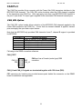
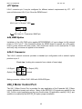
1
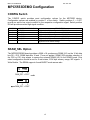
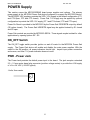
D O C - 0 3 6 5 - 0 1 0
R E V
B .
MPC5553DEMO
Development Board for the Freescale MPC5553
OPTIONS and CONNECTIONS
! Axiom Manufacturing • 2813 Industrial Lane • Garland, TX 75041
Email: [email protected] Web: http://www.axman.com !
M P C 5 5 5 3 D E M O
0 9 / 0 6 / 0 5
CAUTIONARY NOTES ...........................................................................................................................................................3
TERMINOLOGY ......................................................................................................................................................................3
MPC5553DEMO CONFIGURATION....................................................................................................................................4
CONFIG SWITCH .................................................................................................................................................................................................4
SRAM_SEL OPTION ............................................................................................................................................................................................4
POWER SUPPLY......................................................................................................................................................................5
ON_OFF SWITCH ................................................................................................................................................................................................5
PWR - POWER JACK ............................................................................................................................................................................................5
POWER PORT ....................................................................................................................................................................................................6
FUSE – F1 ..........................................................................................................................................................................................................6
VSTBY SWITCH, RV3, AND CT7 ..........................................................................................................................................................................6
ANALOG SUPPLIES .............................................................................................................................................................................................7
USER COMPONENTS .............................................................................................................................................................7
X1 CLOCK OSCILLATOR ......................................................................................................................................................................................7
RV1 AND RV2 USER POTENTIOMETERS ................................................................................................................................................................7
USER LED..........................................................................................................................................................................................................8
USER SWITCH.....................................................................................................................................................................................................8
USER_DEV ........................................................................................................................................................................................................8
SW1 – SW4 PUSH SWITCHES ..............................................................................................................................................................................8
SPEAKER AND SPKR_VOL................................................................................................................................................................................9
MPC5553DEMO I/O PORTS...................................................................................................................................................9
J1 - 10/100TX ETHERNET PORT ..........................................................................................................................................................................9
LNK, SPD, and ACT Indicators .............................................................................................................................................................................................. 9
JP8 JTAG Scan Option ........................................................................................................................................................................................................... 9
J1 Connector ........................................................................................................................................................................................................................... 9
COM-1 PORT.....................................................................................................................................................................................................10
JP2 Option............................................................................................................................................................................................................................. 10
CAN PORT ........................................................................................................................................................................................................11
CAN_SEL Option .................................................................................................................................................................................................................. 11
LIN_J1 ..............................................................................................................................................................................................................12
CT8 Option ............................................................................................................................................................................................................................ 12
JP4 Option............................................................................................................................................................................................................................. 12
JP5 Option............................................................................................................................................................................................................................. 12
JP6 Option............................................................................................................................................................................................................................. 12
JP7 Option............................................................................................................................................................................................................................. 13
LIN_PWR Option .................................................................................................................................................................................................................. 13
LIN-J1 Connector.................................................................................................................................................................................................................. 13
UNI_3 MOTOR CONTROL PORT ..........................................................................................................................................................................13
MOTOR_EN Option.............................................................................................................................................................................................................. 14
UNI_3 Port ............................................................................................................................................................................................................................ 14
HALL ENCODER Port.......................................................................................................................................................................................................... 14
RUN STOP Switch................................................................................................................................................................................................................. 15
RV4 FAULT Adjust and Fault Indicator............................................................................................................................................................................... 15
SW3_UP and SW4_Down ..................................................................................................................................................................................................... 15
TPU PORT .........................................................................................................................................................................................................15
DEVELOPMENT PORTS .................................................................................................................................................................................16
JTAG Port.............................................................................................................................................................................................................................. 16
NEXUS Port .......................................................................................................................................................................................................................... 17
ROBUST Port ........................................................................................................................................................................................................................ 18
JP1 Option............................................................................................................................................................................................................................. 18
MPC5553 I/O HEADER RING..............................................................................................................................................18
A1 – AF4 HEADER...........................................................................................................................................................................................19
A22 – D5 HEADER...........................................................................................................................................................................................19
A23– AF26 HEADER........................................................................................................................................................................................20
AC22– AF5 HEADER .......................................................................................................................................................................................20
2
M P C 5 5 5 3 D E M O
0 9 / 0 6 / 0 5
Cautionary Notes
1) Electrostatic Discharge (ESD) prevention measures should be applied whenever handling
this product. ESD damage is not a warranty repair item.
2) Axiom Manufacturing reserves the right to make changes without further notice to any
products to improve reliability, function or design. Axiom Manufacturing does not assume any
liability arising out of the application or use of any product or circuit described herein; neither
does it convey any license under patent rights or the rights of others.
3) EMC Information on the MPC5553DEMO board:
a) This product as shipped from the factory with associated power supplies and cables, has
been tested and meets with requirements of CE and the FCC as a CLASS A product.
b) This product is designed and intended for use as a development platform for hardware
or software in an educational or professional laboratory.
c) In a domestic environment this product may cause radio interference in which case the
user may be required to take adequate prevention measures.
d) Attaching additional wiring to this product or modifying the products operation from the
factory default as shipped may effect its performance and also cause interference with
other apparatus in the immediate vicinity. If such interference is detected, suitable
mitigating measures should be taken.
Terminology
This development board applies option selection jumpers. Terminology for application of the
option jumpers is as follows:
Jumper on, in, or installed = jumper is a plastic shunt that fits across 2 pins and the
shunt is installed so that the 2 pins are connected with the shunt.
Jumper off, out, or idle = jumper or shunt is installed so that only 1 pin holds the shunt,
no 2 pins are connected, or jumper is removed. It is recommended that the jumpers be
idled by installing on 1 pin so they will not be lost.
This development board applies hardwired option selections (VRL_EN and CUTAWAY 1 – 16).
These option selections apply a circuit trace between the option pads to complete a default
connection. This type connection places an equivalent Jumper Installed type option. The circuit
trace between the option pads maybe cut with a razor blade or similar type knife to isolate the
default connection provided. Applying the default connection again can be performed by
installing the option post pins and shunt jumper, or by applying a wire between the option
pads.
3
M P C 5 5 5 3 D E M O
0 9 / 0 6 / 0 5
MPC5553DEMO Configuration
CONFIG Switch
The CONFIG switch provides reset configuration options for the MPC5553 device.
Configuration options are enabled by position 1 of the switch. Switch positions 2 – 6 OFF
provide an active low output condition to the respective configuration signal. Switch position
ON will provide an active high signal condition.
POSITION
6
5
4
3
2
1
CONFIGURATION SIGNAL
WKPCFG
PLLCFG1
PLLCFG0
BOOTCFG1
BOOTCFG0
CONFIG enable
DESCRIPTION
ON = default, Refer to Freescale MPC5553 Documentation
OFF = default, Refer to Freescale MPC5553 Documentation
ON = default, Refer to Freescale MPC5553 Documentation
OFF = default, Refer to Freescale MPC5553 Documentation
ON = default, Refer to Freescale MPC5553 Documentation
OFF= default. ON = enables the RCON configuration to be
applied from the switch settings.
SRAM_SEL Option
The MPC5553DEMO board provides a 256K x 18 synchronous SRAM (U2) on the 16 bit data
bus D0 – D15. SRAM data bits 16 and 17 are not applied. SRAM_SEL provides selection of
the CS0 or CS1 chip selects to access the external SRAM (U2) on the DEMO board. Chip
select configuration should be set for 0 wait states, 512K byte memory range, WE signals =
Write Enable. The SRAM supports 4 word BURST mode access also.
1
2
3
RAM_CS* = CS1*
1
2
3
RAM_CS* = CS0*
4
M P C 5 5 5 3 D E M O
0 9 / 0 6 / 0 5
POWER Supply
This section covers the MPC5553DEMO board power supplies and options. The primary
power supply is the MC33394 Power Oak device configured to support the MPC5553 device.
The MPC5553 VRC regulator provides the VDD (1.5V) supply in the default configuration (CT1
and CT4 Open, CT2 and CT3 closed). Power Oak 1.5V supply may be applied by optional
configuration to provide the VDD 1.5V supply (CT1 and CT4 closed, CT2 and CT3 open).
Power On Reset is provided to the MPC5553 by the Power Oak PORESETB output by default
(S0 option closed). The Power Oak HRESETB signal may be applied instead by S1 closed
and S0 open.
Power Oak controls are provided by MPC5553 QSPIA. These signals maybe isolated for other
applications by opening options S2 – S5.
ON_OFF Switch
The ON_OFF toggle switch provides ignition on and off control to the MC33394 Power Oak
supply. The Power Oak device will enable and disable the main power supplies. With the
switch in the ON position, all power indicators should light. Inspect input power connection
and source, and fuse F1 if power indication does not occur.
PWR - Power Jack
The Power Jack provides the default power input to the board. The jack accepts a standard
2.0 ~ 2.1mm center barrel plug connector (positive voltage center) to provide the +VIN supply
of +6 to +24 VDC (+12VDC typical).
+Volts, 2mm center
5
M P C 5 5 5 3 D E M O
0 9 / 0 6 / 0 5
POWER Port
Power Port provides access to the main power supplies and Power Oak optional supplies. The
+V connections provided at pins 1 and 2 should be applied for an output voltage source only,
not for input supply.
PIN #
1
3
5
7
9
2
4
6
8
10
11
12
13
15
17
19
21
23
25
24
26
SIGNAL DESCRIPTION
+V = DC input voltage from PWR jack with fuse and polarity protection.
+5V = regulated +5V supply from Power Oak
+3.3V = regulated +3.3V supply from Power Oak
+1.5V = regulated +1.5V supply from Power Oak
VDD = MPC5553 VDD supply, 1.5V typically
Ground / VSS
VSTBY = MPC5553 VSTBY supply, See VSTBY switch option.
RESET* = MPC5553 Reset input signal.
+5VA = MPC5553 Analog supply
VREF1 = Power Oak optional +5V output supply, see MC33394 user guide.
VREF2 = Power Oak optional +5V output supply, see MC33394 user guide.
VREF3 = Power Oak optional +5V output supply, see MC33394 user guide.
VSEN = Power Oak switched +V supply output, see MC33394 user guide
VPRE = Power Oak mains supply prior to regulation, tap, test, or monitor point.
Ground / VSS
Ground / VSS
Note: Pins 14, 16, 18, 20, and 22 not connected.
FUSE – F1
Input power is limited by fuse F1. An 5x20mm type 1A slow-blow type fuse is applied to
protect the DEMO board for overload conditions.
VSTBY Switch, RV3, and CT7
The VSTBY SWITCH provides enabling and disabling the VSTBY operation of the MPC5553
internal RAM. Switch in the OFF position disables the VSTBY operation and the VSTBY pin is
connected to VSS / Ground. Switch in the ON position applies the VKAM standby voltage from
the Power Oak supply to the VSTBY pin.
Potentiometer RV3 provides adjustment of the VSTBY voltage from .75 to 1.25 volts. The
factory setting for RV3 is VSTBY = 1.0 volts and switch is ON.
Cut-away option CT7 allows the user to isolate the VSTBY pin of the MPC5553 from the
switch. With CT7 open, the user must apply external battery or ground to the VSTBY position
on the Power Port connector or I/O header ring.
6
M P C 5 5 5 3 D E M O
0 9 / 0 6 / 0 5
ANALOG Supplies
The MPC5553 +5VA analog supply is provided by the Power Oak VPP regulator output.
Individual noise filters are applied to the +5VA supply to derive the VDDA1 and VDDA2
supplies to the MPC5553. VRH reference supply is provided by +5VA default with the
VRH_EN option jumper installed. External VRH reference may be applied by removing the
VRH_EN option jumper and applying reference voltage at header ring I/O pin A9 or pin 1 of the
option header.
The analog ground supply is also noise filtered and provided to the MPC5553 VSSA pins. VRL
is provided by option VRL_EN which is a cut-away type option.
The QADC digital supply is provided +5V by option CT9. An optional connection to +3.3V for
the QADC is provided by CT10. CT9 must be opened to install CT10 for +3.3V operation. See
the MPC5553 user manual for more details on operating the QADC at +3.#V and limitations of
the VDDA and VRH supplies. The Power Oak may be set via the SPI control port to provide a
+3.3V analog supply on the VPP output. Refer to the MC33394 user manual for details.
USER Components
The DEMO board provides an External clock option (X1), 8 LED indicators, an 8 position DIP
switch, 4 push switches, a speaker with amplifier, and 2 user potentiometers. These devices
are accessed via the USER LED, USER SWITCH, and USER DEV I/O headers. DEMO board
user may apply the devices to the MPC5553 I/O header signals to evaluate operation or assist
in code development.
X1 CLOCK Oscillator
The X1 socket is provided to install standard 5V compatible CAN type clock oscillators so that
alternate clock source or frequencies maybe applied to the MPC5553. User should refer to the
MPC5553 device user manual for information on frequency selection and clocking
configuration.
X1 clock signal is provided to the MPC5553 by option pad set CT16 being closed by 0 ohm
resistor or mod wire application. CUT-AWAY option CT5 must be opened to remove the Y1
crystal from the EXTAL signal or problems may occur with operation. User should review the
MPC5553 user guide for proper PLLCFG0 and PLLCFG1 (CONFIG Switch 4 and 5) option
settings if an external clock is applied.
RV1 and RV2 User Potentiometers
The User Potentiometers provide an adjustable linear voltage output from 0 to 5V. The voltage
signal may be applied to an MPC5553 analog input port for user application.
7
M P C 5 5 5 3 D E M O
0 9 / 0 6 / 0 5
USER LED
User LED header provides access to the user LED 1 to 8. Connector pin 1 to 8 organization is
provided in a one to one method to the individual indicators LED 1 to 8. The LED indicators
are buffered for minimal drive current requirement (~300ua). Indicators will turn on with a logic
high or 2.5 to 5V input at the respective connector pin.
USER Switch
User Switch provides access to the user 8 position DIP Switch. Connector pin 1 to 8
organization is provided in a one to one organization to the individual DIP switch positions 1 to
8. The switch connections are pulled low with 10K ohm resistors when the switch position in
the off position. Switch positions placed in the ON position will provide a 3.3V output to the
connector.
USER_DEV
User DEV provides access to the 4 push switches (SW1 – SW4), speaker, and 2 user
potentiometers (RV1 and RV2).
PIN #
1
2
3
4
5
6
7
8
USER COMPONENT CONNECTION
SW1 out, de-bounced CMOS drive 0 or 3.3V, active low.
SW1 out, de-bounced Open Drain output, active low, 10K ohm pull-up
to 3.3V. Suitable for IRQ input signal drive.
SW2 out, active low, 10K ohm pull-up to 3.3V.
SW3 out, active low, 10K ohm pull-up to 3.3V.
SW4 out, active low, 10K ohm pull-up to 3.3V.
SPEAKER amp input. 0 to 5Vpp, volume adjust with SPKR_VOL.
RV1 center tap, 0 – 5V adjustment
RV2 center tap, 0 – 5V adjustment
SW1 – SW4 Push Switches
The push switches provide momentary active low input for user applications. SW1 has
additional features of being de-bounced for no glitch operation and push-pull output on pin 1 or
open drain output on pin 2. Typical user application would be to provide program control or
menu selection input.
SW3_UP and SW4_Down are also provided for the UNI_3 Port motor control operation when
the MOTOR_EN option is installed.
8
M P C 5 5 5 3 D E M O
0 9 / 0 6 / 0 5
SPEAKER and SPKR_VOL
The speaker and amplifier provide user applications with a method to generate sound effects
from a MPC5553 output. Frequency range of the amplifier input is 300Hz to 10Khz. The
SPKR_VOL potentiometer allows user adjustment of the sound effect volume from the
speaker. The amplifier also provides a SHDN input connection pad. This pad maybe
connected to a MPC5553 output signal to disable the amplifier with a logic high signal of 3.3V
or 5V.
MPC5553DEMO I/O Ports
J1 - 10/100TX Ethernet Port
MPC5553 signals D16 – D31 are applied as the FEC module I/O port for Ethernet 10/100TX
support provided at J1. FEC signals are applied to U11 (DP83848) 10/100TX PHY device.
The J1 port provides AUTO MDIX cable connection detection for standard cross over or
straight through type Ethernet CAT5E cables. Three Ethernet status indicators are provided
for Link, Speed, and Activity. The PHY device may also be included in the JTAG scan signals
by option JP8. Default configuration is PHY not included the scan.
LNK, SPD, and ACT Indicators
Ethernet status is provided by the LNK (Link status), SPD (10 or 100 speed status), and ACT
(transmit status) indicators. All three indicators present Green for the active condition as
follows:
LNK = ON for Ethernet network link detected. No link detected if off.
SPD = ON for 100TX operation. 10TX operation if off.
ACT = ON for MPC5553 transmit activity. Off indicates idle.
The status indicator operation can be modified by MAC PHY commands. Refer to the
DP83848 and MPC5553 user manual for operation details.
JP8 JTAG Scan Option
JP8 is hardwired to exclude the U11 PHY device from the JTAG scan from the JTAG Port. To
include the device in the JATG scan, the user should cut the hardwired trace between JP8 pins
2 and 3, install a .1 space 3 pin header, and a jumper shunt option. With the jumper installed
on JP8 pins 1 and 2, the PHY will be included in the JTAG scan as the 2nd device.
NOTE: JP8 function is disabled on the Revision B DEMO board, do not apply.
J1 Connector
J1 provides the RJ45 style Ethernet 10/100TX port connection.
integrated transformer for network connection.
9
The connector has an
M P C 5 5 5 3 D E M O
0 9 / 0 6 / 0 5
J1 connection
Pin #
1
2
3
4
5
6
7
8
Signal
TX+
TXRX+
TX termination
TX Termination
RXRX Termination
RX Termination
COM-1 Port
COM-1 is a standard RS232 type serial port configured for direct connection to a PC COM Port
with a straight through type 9 pin serial cable. Option JP2 provides MPC5553 SCI channel ‘A’
signal connections when installed. Optional RTS and CTS hardware flow control connection
pads are provided for the user to apply MPC5553 I/O ports and software to enhance operation.
JP2 Option
The JP2 Option provides MPC5553 RXDA and TXDA signals to the COM1 transceiver
connections. This allows the user to apply the provided communication transceiver with the
SCI A channel or to apply the associated I/O to other purposes. JP2 position 1 installed
enables the TXDA output and position 2 enables the RXDA input on COM-1.
COM1
1
TXD
RXD
4
GND
1
2
3
4
5
6
7
8
9
X
The COM-1 port is a Female (socket type) DB9 connector.
6
CTS IN
Pins 1, 4, and 6 connected for status null to host.
RTS OUT
9
Pins 7 and 8 maybe applied by CTS and RTS pads to
MPC5553 I/O.
RTS signal active output level is logic 0. User should place I/O port applied at logic low (0) to
enable the RTS signal and reception of bytes if applied. User should apply a logic high signal
under software control inform host or connected RS232 device to STOP transmitting (stop
sending incoming bytes).
CTS signal active input is level is logic 0. User should apply software to detect a logic high
signal or rising edge on applied I/O port and STOP transmitting bytes to the host or connected
device to implement hardware flow control. Detection of a logic low input indicates the host is
ready to receive bytes and the user may transmit.
DB9 connector pin locations are provided access pads behind the connector on the DEMO
board. User may isolate the connection pads by cutting the associated circuit trace on the
bottom of the board.
10
M P C 5 5 5 3 D E M O
0 9 / 0 6 / 0 5
CAN Port
The CAN Port provides 9 pin connector with the Power Oak CAN transceiver interface to the
MPC5553 CAN channels. The CAN_SEL option locations select the CAN channel is applied
to the transceiver and CAN Port. User may apply more than one MPC5553 CAN channel to
the port if open drain TX output type is applied on the associated CAN channel transmit pins.
CAN_SEL Option
The CAN_SEL option header allows selection of the MPC5553 CAN channels applied to the
Power Oak transceiver and CAN Port. If more that one transmit channel is applied, transmit
pins must apply the open drain output feature.
Note that the MPC5553 only provides CAN channels A and C, channel B support is provided
for MPC5554.
POSITION #
1
2
3
4
5
6
MPC5553 CAN SIGNAL
CNTX_A, channel A TX out (DEFAULT enabled)
CNRX_A, channel A RX in (DEFAULT enabled)
CNTX_B, channel B TX out (N/A with MPC5553)
CNRX_B, channel B RX in (N/A with MPC5553)
CNTX_C, channel C TX out
CNRX_C, channel C RX in
Following is the DB9S connection reference.
CAN_PORT
1
CAN_LO
GND
4
5
1
2
3
4
5
6
7
8
9
X
GND
CAN_HI
8
9
CAN port has a Female (socket type) DB9
connector.
CAN_HI and CAN_LO signals are terminated together with 120 ohms (R68).
DB9 connector pin locations are provided access pads behind the connector on the DEMO
board for additional user application.
11
M P C 5 5 5 3 D E M O
0 9 / 0 6 / 0 5
LIN_J1
The LIN_J1 port provides a Master Mode LIN network connection. The MPC5553 device
provides a LIN Master type node on the LIN Network. A LIN physical layer transceiver U7
(MC33661, or similar) is provided between the MPC5553 device and the LIN network
connector. Refer to the MC33661 data sheet for complete details of transceiver operation. The
following diagram represents the LIN connection:
MPC5553
MC33661
RXDB
JP5
LIN-J1
TXDB
JP6
The LIN interface provides optional features of slew rate control, network supply, and wake up
option. See the JP4, JP5, JP6, JP7 and CT8 options following.
CT8 Option
MPC5553 I/O signal GPIO205 provides LIN transceiver U7 enable control (EN pin). Software
control of the EN pin allows the user to set the slew rate control of the transceiver. User
applications should configure the GPIO205 pin for output to operate the LIN transceiver. If
GPIO205 is needed for other purposes, the CT8 option maybe cut to isolate the signal from the
LIN transceiver and JP4 installed to provide an enable to the transceiver. Refer to the
MC33361 data sheet for further details of operation.
JP4 Option
Installation of JP4 applies a pull-up resistor on the LIN transceiver enable pin. MPC5553
GPIO205 may still control the transceiver enable operation when JP4 is installed.
JP5 Option
JP5 selects the MPC5553 SCI RXDB signal input to be from the LIN transceiver. For LIN
operation JP5 must be installed.
JP6 Option
JP6 is wired closed by default and not populated. JP6 provides the MPC5553 TXDB signal to
the LIN transceiver. User may cut the JP6 wire trace to isolate the TXDB signal.
12
M P C 5 5 5 3 D E M O
0 9 / 0 6 / 0 5
JP7 Option
LIN-J1 connector pin 2 may be configured for different network requirements by JP7. JP7
open will disconnect LIN-J1 pin 2 from the DEMO board.
1
2
3
LIN-J1 pin 2 = Ground / VSS
1
2
3
LIN-J1 pin 2 = Transceiver WAKE pin
LIN_PWR Option
Installation of the LIN_PWR option applies MPC5553DEMO +V input voltage for LIN network
power to LIN-J1 pin 3. This connection allows the DEMO board to operate as a LIN master
node to power remote LIN slave nodes. User should use caution to not overload the F1 fuse
and verify only one source is applied on the network.
LIN-J1 Connector
The LIN-J1 network connector provides a standard pin configuration with a network option
position on pin 2.
Front view (looking into connector from outside of board edge)
LIN Signal
4
3
+V Output (JP5)
Option (JP4) 2
1
Ground
Mating connector = Molex 39-01-2040 with 39-00-0039 pins.
UNI_3 Motor Control Port
The UNI_3 Motor Control Port is provided for easy application of the Freescale UNI_3 Motor
control application boards and motors. Many of the MPC5553 I/O signals are applied for the
UNI_3 motor control application so the user should review I/O application carefully. UNI_3 port
operation is enabled by the MOTOR_EN option jumper installation.
13
M P C 5 5 5 3 D E M O
0 9 / 0 6 / 0 5
MOTOR_EN Option
This option controls the connection of the MPC5553 I/O ports to the UNI_3 and
HALL_ENCODER motor control ports. When installed, signal buffers U13 and U15 are
enabled to apply MPC5553 I/O for motor control.
UNI_3 Port
The UNI_3 port is the primary motor control I/O port for application of the UNI_3 motor control
development boards. Following are the signal assignments:
MPC5553 Signal
TPU_A8
TPU_A9
TPU_A10
TPU_A11
TPU_A12
TPU_A13
VSS / GROUND
VSSA
AN16
AN18
AN20
TPU_A15
TPU_A6
AN22
UNI_3 Signal
PWM_AT
PWM_AB
PWM_BT
PWM_BB
PWM_CT
PWM_CB
GROUND
x
ANALOG GND
x
VS_DCB
IS_A
IS_C
x
BRAKE
x
x
ZX_B
x
BEMF_B
UNI_3 Port
1
3
5
7
9
11
13
15
17
19
21
23
25
27
29
31
33
35
37
39
2
4
6
8
10
12
14
16
18
20
22
24
26
28
30
32
34
36
38
40
UNI_3 Signal
Common 4,6,8,10
Common 2,6,8,10
Common 2,4,8,10
Common 2,4,6,10
Common 2,4,6,8
GROUND
x
x
ANALOG GND
x
IS_DCB
ISB
x
x
x
x
ZX_A
ZX_C
BEMF_A
BEMF_C
MPC5553
Signal
x
x
x
x
x
VSS / GROUND
VSSA
AN17
AN19
TPU_A5
TPU_A7
AN21
AN23
HALL ENCODER Port
The Hall encoder port is provided for motor position feedback signals from the UNI_3 motor
application development boards.
HALL
Port
1
2
3
4
5
6
x
HALL
Signal
+5V
GROUND
H_1
H_2
H_3
H_4
H_CLK
MPC5553 Signal
+5V / VDDH
VSS / GROUND
TPU_A1
TPU_A2
TPU_A3
TPU_A4
TCRCLK_A, H_CLK is derived by logic from the H_1 – 4 signals.
14
M P C 5 5 5 3 D E M O
0 9 / 0 6 / 0 5
RUN STOP Switch
The RUN STOP switch is connected to the MPC5553 EMIOS11 signal pin. The switch
provides a motor run or stop condition input for the motor control application.
RV4 FAULT Adjust and Fault Indicator
RV4 Fault Adjustment is provided to set the applied motor over-current fault condition. The
IS_DCB current sense input from the UNI_3 port is compared by U16 with the RV4 setting to
determine if an over-current condition exists. If the IS_DCB input signal is greater than the RV4
setting, the Fault condition becomes active. The FAULT indicator will light and an active low
Fault signal will be provided to MPC5553 EMIOS10 signal pin.
SW3_UP and SW4_Down
User switches SW3 and SW4 provide the motor speed UP and DOWN input signals when the
MOTOR_EN option is installed. Both switches are active low. SW3_UP signal is provided to
the MPC5553 EMIOS8 signal pin. SW4_DOWN signal is provided to the MPC5553 EMIOS9
signal pin.
TPU Port
The TPU_PORT provides an organized I/O port for the MPC5553 TPU_A signals.
MPC5553 Signal
+3.3V
ETPU_A16
ETPU_A17
ETPU_A18
ETPU_A19
ETPU_A20
ETPU_A21
ETPU_A22
ETPU_A23
ETPU_A24
ETPU_A25
ETPU_A26
ETPU_A27
ETPU_A28
ETPU_A29
ETPU_A30
ETPU_A31
GND
TCRCLK_A
GND
TPU Port
1
2
3
4
5
6
7
8
9
10
11
12
13
14
15
16
17
18
19
20
21
22
23
24
25
26
27
28
29
30
31
32
33
34
35
36
37
38
39
40
MPC5553 Signal
+5V
x
x
ETPU_A0
ETPU_A1
ETPU_A2
ETPU_A3
ETPU_A4
ETPU_A5
ETPU_A6
ETPU_A7
ETPU_A8
ETPU_A9
ETPU_A10
ETPU_A11
ETPU_A12
ETPU_A13
ETPU_A14
ETPU_A15
GND
15
M P C 5 5 5 3 D E M O
0 9 / 0 6 / 0 5
DEVELOPMENT PORTS
The MPC5553DEMO board provides 1 JTAG and 2 NEXUS type development ports. Only
one of the development ports should be applied due to common signals used on the ports.
The development port input and power signals are buffered by a CBTLV3861 device. This
buffer provides a bi-directional 5 ohms series resistance on the input signals when powered
on. The buffer also provides signal isolation when powered off.
NOTE: Proper power sequencing must be performed when a development port is
applied (cable connected). Development port application power sequence:
1) MPC5553DEMO board ON–OFF switch is OFF and no power is applied to the PWR
connector.
2) Connect development port cable to the desired MPC5553DEMO board development port.
3) Apply power to the MPC5553DEMO board PWR connector and turn ON–OFF switch ON.
4) If power is removed or the ON-OFF switch is turned off, remove development cable from
board connector and re-apply from step 1 of this procedure.
JTAG Port
The JTAG port provides a Freescale standard JTAG connection to the MPC5553. The
connector is a standard 2x7, .1 inch pin space keyed pin header. Example compatible cables
include the OCDEMON™ NP-JTAG ONCE “Wiggler” and the P&E Microcomputer Systems
CABPPCNEXUS. Host software must be applied to operate the cables.
JTAG Port
Signal
B_TDI
TDO
B-TCK
JTG7 TP
B-RESET*
B_+3.3V
B_RDY*
Pin #
1
3
5
7
9
11
13
Pin #
2
4
6
8
10
12
14
Signal
GND
GND
GND
JTG8 TP
B_TMS
GND
B_JCOMP
Notes:
1) B_… signals are buffered.
2) JTGx TP signals are not connected to the MPC5553 and provide a Test Pad on the board.
3) Signals followed by a “*” symbol are active logic low.
4) See the J1 Ethernet section about JP8 and the PHY device JTAG.
16
M P C 5 5 5 3 D E M O
0 9 / 0 6 / 0 5
NEXUS Port
The NEXUS port provides a more powerful and higher speed development port for high end
tools. The port connector is an AMP 38 pin Mictor style, part number #767053-1.
NEXUS Port
Signal
NXS1 TP
NXS3 TP
MDO9
BOOTCFG1
B_RESET*
TDO
MDO10
B_TCK
B_TMS
B_TDI
B_JCOMP
MDO11
ERSTOUT*
NXS27 TP
NXS29 TP (Note 3)
+V
+V
NXS35 TP (Note 3)
B_VSTBY
Pin #
1
3
5
7
9
11
13
15
17
19
21
23
25
27
29
31
33
35
37
Pin #
2
4
6
8
10
12
14
16
18
20
22
24
26
28
30
32
34
36
38
Signal
NXS2 TP
NXS4 TP
CLKOUT
MDO8
B_EVTI*
B_+3.3V
B_RDY*
MDO7
MDO6
MDO5
MDO4
MDO3
MDO2
MDO1
MDO0
EVTO*
MCKO
MSEO1*
MSEO0*
Notes:
1) B_… signals are buffered.
2) NXSxx TP signals are not connected to the MPC5553 and provide a Test Pad on the
board.
3) NXSxx signal TP is also connected to the ROBUST Nexus connector.
4) Signals followed by a “*” symbol are active logic low.
17
M P C 5 5 5 3 D E M O
0 9 / 0 6 / 0 5
ROBUST Port
The ROBUST port connector location is provided for user expansion. This port provides the
ROBUST Nexus 51 pin location that applies the GLENAIR MR7580-51P2BNU connector.
ROBUST Port
Pin #
1
2
3
4
5
6
7
8
9
10
11
12
13
14
15
16
17
18
Signal
+V
+V
B_VSTBY1
NXS35 TP
TDO
B_RDY*
B_RESET*
B_+3.3V
B_EVTI*
GND
B_JCOMP
GND
B_TMS
GND
B_TDI
GND
B_TCK
GND
Pin #
19
20
21
22
23
24
25
26
27
28
29
30
31
32
33
34
35
Signal
MDO0
GND
MCKO
GND
EVTO*
GND
MSEO0*
MDO9
MDO1
GND
MDO2
GND
MDO3
GND
NXS29 TP
GND
MSEO1*
Pin #
36
37
38
39
40
41
42
43
44
45
46
47
48
49
50
51
Signal
GND
MDO4
GND
MDO5
GND
MDO6
GND
MDO7
GND
MDO8
GND
MDO10
GND
MDO11
GND
JP1 pin 2
Notes:
1) NXS29 and NXS35 signals are also connected to the NEXUS connector.
2) Signals followed by a “*” symbol are active logic low.
JP1 Option
JP1 provides signal selection for the Robust Nexus connector pin 51. Position 1-2 provides
the BOOTCFG1 signal and position 2-3 provides the ERSTOUT* signal.
1
2
3
Robust pin 51 = ERSTOUT*
1
2
3
Robust pin 51 = BOOTCFG1
MPC5553 I/O HEADER RING
MPC5553 I/O signals are provided by the I/O header ring. The header ring consists of .1 inch grid pins organized
in 4 rows for each side of the MPC5553 device. Each row reflects the corresponding location of the MPC5553
device BGA package ball ring. Signals indicated are the DEMO board primary function.
18
M P C 5 5 5 3 D E M O
0 9 / 0 6 / 0 5
A1 – AF4 HEADER
PIN
A1
B1
C1
D1
SIGNAL
GND
VDD
3.3V
TPU_A30
PIN
A2
B2
C2
D2
E1
TPU_A28
E2
F1
TPU_A24
F2
G1
TPU_A23
G2
H1
TPU_A20
H2
J1
TPU_A16
J2
K1
TPU_A12
K2
L1
M1
N1
P1
R1
T1
U1
V1
W1
Y1
AA1
AB1
AC1
AD1
AE1
AF1
TPU_A8
TPU_A4
BDIP*
CS3*
WE3*
3.3V
A16
A18
A20
A22
A24
3.3V
A26
A28
A29
GND
L2
M2
N2
P2
R2
T2
U2
V2
W2
Y2
AA2
AB2
AC2
AD2
AE2
AF2
SIGNAL
VSTBY
GND
VDD
TPU_A3
1
TPU_A2
9
TPU_A2
7
TPU_A2
2
TPU_A1
9
TPU_A1
5
TPU_A1
1
TPU_A7
TPU_A3
TEA*
CS2*
WE2*
TSIZ0
TSIZ1
A17
A19
A21
A23
A25
A27
A30
GND
VDD
PIN
A3
B3
C3
D3
SIGNAL
AN37
AN36
GND
VDD
PIN
A4
B4
C4
D4
SIGNAL
AN11
AN39
AN8
GND
E3
5V
E4
VDD
F3
TPU_A2
6
TPU_A2
5
TPU_A1
8
TPU_A1
4
TPU_A1
0
TPU_A6
TPU_A2
TPU_A0
CS1*
WE1*
RD_WR
TA*
TS*
A9
A11
A13
A15
A31
GND
VDD
TX_CLK
F4
5V
G4
TPU_A21
H4
TPU_A17
J4
TPU_A13
K4
TPU_A9
L4
M4
N4
P4
R4
T4
U4
V4
W4
Y4
AA4
AB4
AC4
AD4
AE4
AF4
TPU_A5
TPU_A1
TCRCLK_A
CS0*
WE0*
3.3V
3.3V
A8
A10
3.3V
A12
A14
GND
VDD
CRS
TX_ER
G3
H3
J3
K3
L3
M3
N3
P3
R3
T3
U3
V3
W3
Y3
AA3
AB3
AC3
AD3
AE3
AF3
A22 – D5 HEADER
PIN
A22
A21
A20
A19
A18
A17
A16
A15
A14
A13
A12
A11
A10
A9
A8
A7
A6
A5
SIGNAL
MDO11
GPIO205
x
x
x
x
ETRIG1
AN15
VSSA
AN35
AN28
AN27
AN23
VRH
AN5_AND2AN1_AND0AN16
VDDA1
PIN
B22
B21
B20
B19
B18
B17
B16
B15
B14
B13
B12
B11
B10
B9
B8
B7
B6
B5
SIGNAL
MDO7
MDO10
x
x
x
x
ETRIG0
AN14
VSSA
AN32
AN31
AN26
AN22
x
AN4_AND2+
AN0_AND0+
AN20
AN19
PIN
C22
C21
C20
C19
C18
C17
C16
C15
C14
C13
C12
C11
C10
C9
C8
C7
C6
C5
SIGNAL
MDO3
MDO6
MDO9
x
x
x
x
AN13
VDDA0
AN33
AN30
AN25
VRL
AN7_DAN3AN3_DAN1AN21
VSSA
AN17
19
PIN
D22
D21
D20
D19
D18
D17
D16
D15
D14
D13
D12
D11
D10
D9
D8
D7
D6
D5
SIGNAL
5V
MDO2
MDO5
x
x
x
x
AN12
5V
AN34
AN29
AN24
AN6_DAN3+
AN2_DAN1+
AN18
AN10
AN9
AN38
M P C 5 5 5 3 D E M O
0 9 / 0 6 / 0 5
A23– AF26 HEADER
PIN
A23
B23
C23
D23
E23
F23
G23
H23
J23
K23
L23
M23
N23
P23
R23
T23
U23
V23
W23
Y23
AA23
AB23
AC23
AD23
AE23
AF23
SIGNAL
MDO8
MDO4
MDO1
GND
3.3V
MSEO0*
MSEO1*
RDY*
5V
x
x
x
SOUT_B
SIN_D
PCS_B5
PCS_B2
SOUT_D
CNTX_C
RXDB
WKPCFG
5V
VDD
GND
NC2
3.3V
PCS_C4
PIN
A24
B24
C24
D24
E24
F24
G24
H24
J24
K24
L24
M24
N24
P24
R24
T24
U24
V24
W24
Y24
AA24
AB24
AC24
AD24
AE24
AF24
SIGNAL
VDD
MDO0
GND
3.3V
TMS
JCOMP
MCKO
GPIO203
x
x
x
x
PCS_B3
PCS_B4
PCS_C5
PCS_D2
TXDA
RXDA
CNRX_C
BOOTCFG1
PLLCFG1
x (VRCCTL)
VDD
GND
CLKOUT
3.3V
PIN
A25
B25
C25
D25
E25
F25
G25
H25
J25
K25
L25
M25
N25
P25
R25
T25
U25
V25
W25
Y25
AA25
AB25
AC25
AD25
AE25
AF25
SIGNAL
3.3V
GND
3.3V
TCK
TDO
EVTI*
GPIO204
x
x
x
x
x
PCS_B0
SCK_B
PCS_C2
SCK_D
PCS_B3
RSTOUT*
TXDB
GND
BOOTCFG0
PLLCFG0
VRC33
VDD
GND
ENGCLK
PIN
A26
B26
C26
D26
E26
F26
G26
H26
J26
K26
L26
M26
N26
P26
R26
T26
U26
V26
W26
Y26
AA26
AB26
AC26
AD26
AE26
AF26
SIGNAL
GND
3.3V
VDD
TDI
TEST*
EVTO*
x
x
x
x
x
SIN_B
PCS_B1
PCS_B2
PCS_C1
5V
3.3V
RSTCFG*
RESET*
GND
x (EXTAL)
x (XTAL)
x (VDDSYN)
3.3V
VDD
GND
AC22– AF5 HEADER
PIN
AC22
AC21
SIGNAL
NC11
3.3V
PIN
AD22
AD21
SIGNAL
3.3V
CNTX_A
PIN
AE22
AE21
SIGNAL
CNRX_A
EMIOS23
PIN
AF22
AF21
AC20
5V
AD20
EMIOS22
AE20
EMIOS19
AF20
AC19
EMIOS21
AD19
EMIOS17
AE19
EMIOS16
AF19
AC18
EMIOS12
AD18
EMIOS15
AE18
EMIOS13
AF18
AC17
AC16
AC15
AC14
AC13
AC12
AC11
AC10
AC9
AC8
AC7
AC6
AC5
EMIOS8
EMIOS2
D14
D12
3.3V
D10
D8
RXD3
RXD2
3.3V
TXD1
TX_EN
VDD
AD17
AD16
AD15
AD14
AD13
AD12
AD11
AD10
AD9
AD8
AD7
AD6
AD5
EMIOS10
EMIOS6
EMIOS3
D15
D13
D11
D9
GPIO207
3.3V
RXD1
TXD2
RX_DV
COL
AE17
AE16
AE15
AE14
AE13
AE12
AE11
AE10
AE9
AE8
AE7
AE6
AE5
EMIOS9
EMIOS5
EMIOS1
MDIO
MDC
OE*
D6
D4
D2
D0
TXD3
RX_ER
RX_CLK
AF17
AF16
AF15
AF14
AF13
AF12
AF11
AF10
AF9
AF8
AF7
AF6
AF5
Note: Indicated as AF22 / AF5 on DEMO board.
20
SIGNAL
PCS_C3
EMIOS2
0
EMIOS1
8
EMIOS1
4
EMIOS1
1
EMIOS7
EMIOS4
EMOS0
BB*
D7
D5
3.3V
D3
D1
GPIO206
RXD0
TXD0
3.3V