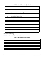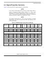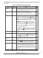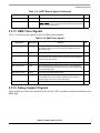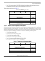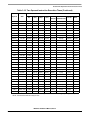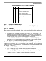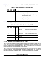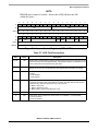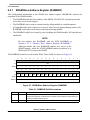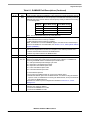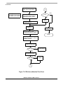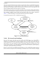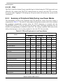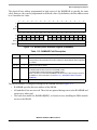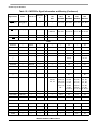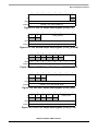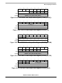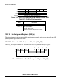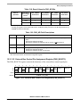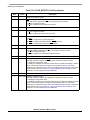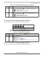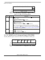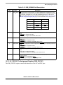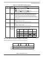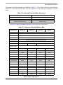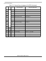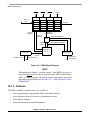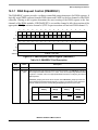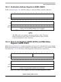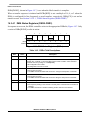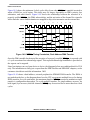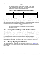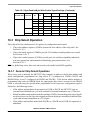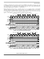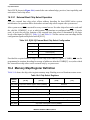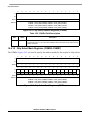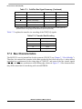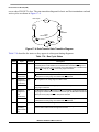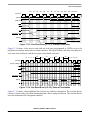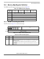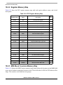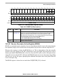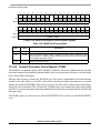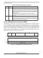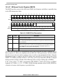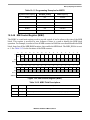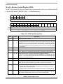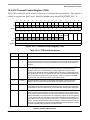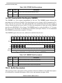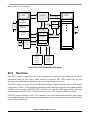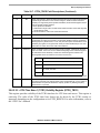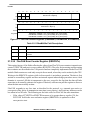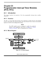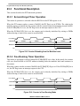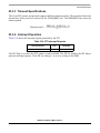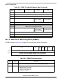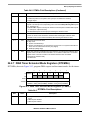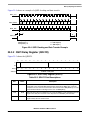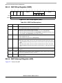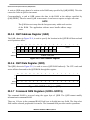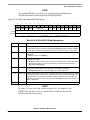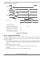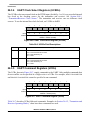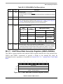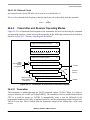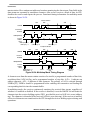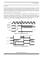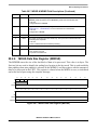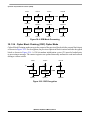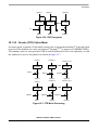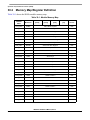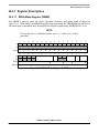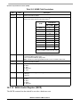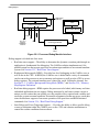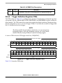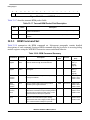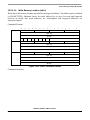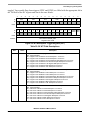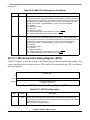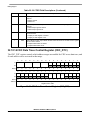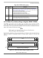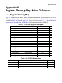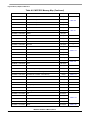
1
MCF5235 Reference Manual
Devices Supported:
MCF5232
MCF5233
MCF5234
MCF5235
Document Number: MCF5235RM
Rev. 2
07/2006
How to Reach Us:
Home Page:
www.freescale.com
E-mail:
[email protected]
USA/Europe or Locations Not Listed:
Freescale Semiconductor
Technical Information Center, CH370
1300 N. Alma School Road
Chandler, Arizona 85224
+1-800-521-6274 or +1-480-768-2130
[email protected]
Europe, Middle East, and Africa:
Freescale Halbleiter Deutschland GmbH
Technical Information Center
Schatzbogen 7
81829 Muenchen, Germany
+44 1296 380 456 (English)
+46 8 52200080 (English)
+49 89 92103 559 (German)
+33 1 69 35 48 48 (French)
[email protected]
Japan:
Freescale Semiconductor Japan Ltd.
Headquarters
ARCO Tower 15F
1-8-1, Shimo-Meguro, Meguro-ku,
Tokyo 153-0064, Japan
0120 191014 or +81 3 5437 9125
[email protected]
Asia/Pacific:
Freescale Semiconductor Hong Kong Ltd.
Technical Information Center
2 Dai King Street
Tai Po Industrial Estate
Tai Po, N.T., Hong Kong
+800 26668334
[email protected]
For Literature Requests Only:
Freescale Semiconductor Literature Distribution Center
P.O. Box 5405
Denver, Colorado 80217
1-800-441-2447 or 303-675-2140
Fax: 303-675-2150
[email protected]
Information in this document is provided solely to enable system and
software implementers to use Freescale Semiconductor products. There are
no express or implied copyright licenses granted hereunder to design or
fabricate any integrated circuits or integrated circuits based on the
information in this document.
Freescale Semiconductor reserves the right to make changes without further
notice to any products herein. Freescale Semiconductor makes no warranty,
representation or guarantee regarding the suitability of its products for any
particular purpose, nor does Freescale Semiconductor assume any liability
arising out of the application or use of any product or circuit, and specifically
disclaims any and all liability, including without limitation consequential or
incidental damages. “Typical” parameters that may be provided in Freescale
Semiconductor data sheets and/or specifications can and do vary in different
applications and actual performance may vary over time. All operating
parameters, including “Typicals”, must be validated for each customer
application by customer’s technical experts. Freescale Semiconductor does
not convey any license under its patent rights nor the rights of others.
Freescale Semiconductor products are not designed, intended, or authorized
for use as components in systems intended for surgical implant into the body,
or other applications intended to support or sustain life, or for any other
application in which the failure of the Freescale Semiconductor product could
create a situation where personal injury or death may occur. Should Buyer
purchase or use Freescale Semiconductor products for any such unintended
or unauthorized application, Buyer shall indemnify and hold Freescale
Semiconductor and its officers, employees, subsidiaries, affiliates, and
distributors harmless against all claims, costs, damages, and expenses, and
reasonable attorney fees arising out of, directly or indirectly, any claim of
personal injury or death associated with such unintended or unauthorized
use, even if such claim alleges that Freescale Semiconductor was negligent
regarding the design or manufacture of the part.
Freescale™ and the Freescale logo are trademarks of Freescale
Semiconductor, Inc. All other product or service names are the property
of their respective owners.© Freescale Semiconductor, Inc. 2006. All rights
reserved.
MCF5235RM
Rev. 2
07/2006
Overview
Signal Descriptions
ColdFire Core
Enhanced Multiply-Accumulate Unit (EMAC)
Cache
Static RAM (SRAM)
Clock Module
Power Management
Chip Configuration Module (CCM)
Reset Controller Module
System Control Module (SCM)
General Purpose I/O Module
Interrupt Controller Modules
DMA Controller Module
Edge Port Module (EPORT)
Chip Select Module
External Interface Module (EIM)
Synchronous DRAM Controller
Fast Ethernet Controller (FEC)
Enhanced Time Processing Unit (eTPU)
FlexCAN
Watchdog Timer Module
Programmable Interrupt Timers (PITs)
DMA Timers
Queued Serial Peripheral Interface (QSPI)
UART Modules
I2C interface
Message Digest Hardware Accelerator (MDHA)
Random Number Generator (RNG)
Symmetric Key Hardware Accelerator (SKHA)
IEEE 1149.1 Test Access Port (JTAG)
Debug Support
Register Memory Map Quick Reference
Index
1
2
3
4
5
6
7
8
9
10
11
12
13
14
15
16
17
18
19
20
21
22
23
24
25
26
27
28
29
30
31
32
A
IND
1
2
3
4
5
6
7
8
9
10
11
12
13
14
15
16
17
18
19
20
21
22
23
24
25
26
27
28
29
30
31
32
A
IND
Overview
Signal Descriptions
ColdFire Core
Enhanced Multiply-Accumulate Unit (EMAC)
Cache
Static RAM (SRAM)
Clock Module
Power Management
Chip Configuration Module (CCM)
Reset Controller Module
System Control Module (SCM)
General Purpose I/O Module
Interrupt Controller Modules
DMA Controller Module
Edge Port Module (EPORT)
Chip Select Module
External Interface Module (EIM)
Synchronous DRAM Controller
Fast Ethernet Controller (FEC)
Enhanced Time Processing Unit (eTPU)
FlexCAN
Watchdog Timer Module
Programmable Interrupt Timers (PITs)
DMA Timers
Queued Serial Peripheral Interface (QSPI)
UART Modules
I2C interface
Message Digest Hardware Accelerator (MDHA)
Random Number Generator (RNG)
Symmetric Key Hardware Accelerator (SKHA)
IEEE 1149.1 Test Access Port (JTAG)
Debug Support
Register Memory Map Quick Reference
Index
Contents
Paragraph
Number
Title
Page
Number
Chapter 1
Overview
1.1
1.2
1.3
1.3.1
1.3.2
1.3.3
1.3.3.1
1.3.4
1.3.5
1.3.6
1.3.6.1
1.3.6.2
1.3.7
1.3.8
1.3.9
1.3.10
1.3.11
1.3.12
1.3.13
1.3.14
1.3.15
1.3.16
1.3.17
1.3.18
1.3.19
1.3.20
1.3.21
1.3.22
1.4
MCF5235 Family Configurations ................................................................................... 1-2
Block Diagram ................................................................................................................ 1-3
Features ........................................................................................................................... 1-5
Feature Overview ........................................................................................................ 1-5
V2 Core Overview ...................................................................................................... 1-9
Enhanced Time Processor Unit (eTPU) ...................................................................... 1-9
eTPU Functions .................................................................................................... 1-10
Integrated Debug Module ......................................................................................... 1-11
JTAG ......................................................................................................................... 1-12
On-chip Memories .................................................................................................... 1-12
Cache .................................................................................................................... 1-12
SRAM ................................................................................................................... 1-13
Fast Ethernet Controller (FEC) ................................................................................. 1-13
FlexCAN ................................................................................................................... 1-13
UARTs ...................................................................................................................... 1-13
I2C Bus ...................................................................................................................... 1-14
QSPI .......................................................................................................................... 1-14
Cryptography ............................................................................................................ 1-14
DMA Timers (DTIM0-DTIM3) ............................................................................... 1-14
Periodic Interrupt Timers (PIT0-PIT3) ..................................................................... 1-14
Software Watchdog Timer ........................................................................................ 1-14
Clock Module and Phase Locked Loop (PLL) ......................................................... 1-15
Interrupt Controllers (INTC0, INTC1) ..................................................................... 1-15
DMA Controller ........................................................................................................ 1-15
External Interface Module (EIM) ............................................................................. 1-15
SDRAM Controller ................................................................................................... 1-16
Reset .......................................................................................................................... 1-16
GPIO ......................................................................................................................... 1-16
Documentation .............................................................................................................. 1-17
Chapter 2
Signal Descriptions
2.1
2.1.1
Introduction ..................................................................................................................... 2-1
Overview ..................................................................................................................... 2-1
MCF5235 Reference Manual, Rev. 2
Freescale Semiconductor
v
Contents
Paragraph
Number
2.2
2.3
2.3.1
2.3.2
2.3.3
2.3.4
2.3.5
2.3.6
2.3.7
2.3.8
2.3.9
2.3.10
2.3.11
2.3.12
2.3.13
2.3.14
2.3.15
2.3.16
2.4
Title
Page
Number
Signal Properties Summary ............................................................................................ 2-3
Signal Primary Functions ................................................................................................ 2-8
Reset Signals ............................................................................................................... 2-8
PLL and Clock Signals ............................................................................................... 2-9
Mode Selection ........................................................................................................... 2-9
External Memory Interface Signals ............................................................................ 2-9
SDRAM Controller Signals ...................................................................................... 2-11
External Interrupt Signals ......................................................................................... 2-11
eTPU ......................................................................................................................... 2-11
Ethernet Module (FEC) Signals ................................................................................ 2-12
Feature Control ......................................................................................................... 2-13
I2C I/O Signals ......................................................................................................... 2-13
Queued Serial Peripheral Interface (QSPI) ............................................................... 2-14
UART Module Signals ............................................................................................. 2-14
DMA Timer Signals .................................................................................................. 2-15
Debug Support Signals ............................................................................................. 2-15
Test Signals ............................................................................................................... 2-17
Power and Ground Pins ............................................................................................ 2-17
External Boot Mode ...................................................................................................... 2-17
Chapter 3
ColdFire Core
3.1
3.2
3.2.1
3.2.1.1
3.2.1.2
3.2.1.3
3.2.1.4
3.2.1.5
3.2.2
3.2.3
3.2.3.1
3.2.3.2
3.2.3.3
3.2.3.4
3.2.3.5
3.2.3.6
3.3
3.4
Processor Pipelines ......................................................................................................... 3-1
Processor Register Description ....................................................................................... 3-2
User Programming Model .......................................................................................... 3-2
Data Registers (D0–D7) ......................................................................................... 3-2
Address Registers (A0–A6) .................................................................................... 3-3
Stack Pointer (A7) .................................................................................................. 3-3
Program Counter (PC) ............................................................................................ 3-3
Condition Code Register (CCR) ............................................................................. 3-4
EMAC Register Description ....................................................................................... 3-4
Supervisor Register Description ................................................................................. 3-5
Status Register (SR) ................................................................................................ 3-6
Supervisor/User Stack Pointers (A7 and OTHER_A7) .......................................... 3-7
Vector Base Register (VBR) .................................................................................. 3-7
Cache Control Register (CACR) ............................................................................ 3-7
Access Control Registers (ACR0, ACR1) .............................................................. 3-8
SRAM Base Address Register (RAMBAR) ........................................................... 3-8
Memory Map/Register Definition .................................................................................. 3-8
Additions to the Instruction Set Architecture ................................................................. 3-9
MCF5235 Reference Manual, Rev. 2
vi
Freescale Semiconductor
Contents
Paragraph
Number
3.5
3.6
3.7
3.7.1
3.7.2
3.7.3
3.7.4
3.7.5
3.7.6
3.7.7
3.7.8
3.7.9
3.7.10
3.7.11
3.7.12
3.7.13
3.7.14
3.8
3.8.1
3.8.2
3.9
3.10
3.11
3.12
3.13
3.14
Title
Page
Number
Exception Processing Overview ..................................................................................... 3-9
Exception Stack Frame Definition ................................................................................ 3-11
Processor Exceptions .................................................................................................... 3-13
Access Error Exception ............................................................................................ 3-13
Address Error Exception ........................................................................................... 3-13
Illegal Instruction Exception ..................................................................................... 3-13
Divide-By-Zero ......................................................................................................... 3-14
Privilege Violation .................................................................................................... 3-14
Trace Exception ........................................................................................................ 3-14
Unimplemented Line-A Opcode ............................................................................... 3-15
Unimplemented Line-F Opcode ............................................................................... 3-15
Debug Interrupt ......................................................................................................... 3-15
RTE and Format Error Exception ............................................................................. 3-15
TRAP Instruction Exception ..................................................................................... 3-15
Interrupt Exception ................................................................................................... 3-15
Fault-on-Fault Halt ................................................................................................... 3-16
Reset Exception ........................................................................................................ 3-16
Instruction Execution Timing ....................................................................................... 3-19
Timing Assumptions ................................................................................................. 3-19
MOVE Instruction Execution Times ........................................................................ 3-20
Standard One Operand Instruction Execution Times ................................................... 3-21
Standard Two Operand Instruction Execution Times ................................................... 3-22
Miscellaneous Instruction Execution Times ................................................................. 3-24
EMAC Instruction Execution Times ............................................................................ 3-25
Branch Instruction Execution Times ............................................................................ 3-26
ColdFire Instruction Set Architecture Enhancements .................................................. 3-26
Chapter 4
Enhanced Multiply-Accumulate Unit (EMAC)
4.1
4.2
4.3
4.4
4.4.1
4.4.1.1
4.4.2
4.5
4.5.1
4.5.2
4.5.3
Multiply-Accumulate Unit .............................................................................................. 4-1
Introduction to the MAC ................................................................................................. 4-2
General Operation ........................................................................................................... 4-3
Memory Map/Register Definition .................................................................................. 4-6
MAC Status Register (MACSR) ................................................................................. 4-6
Fractional Operation Mode ..................................................................................... 4-9
Mask Register (MASK) ............................................................................................ 4-11
EMAC Instruction Set Summary .................................................................................. 4-12
EMAC Instruction Execution Times ........................................................................ 4-13
Data Representation .................................................................................................. 4-14
MAC Opcodes .......................................................................................................... 4-14
MCF5235 Reference Manual, Rev. 2
Freescale Semiconductor
vii
Contents
Paragraph
Number
Title
Page
Number
Chapter 5
Cache
5.1
5.1.1
5.1.2
5.1.3
5.1.3.1
5.1.3.2
5.1.3.3
5.1.3.4
5.1.3.5
5.2
5.2.1
5.2.1.1
5.2.1.2
Introduction ..................................................................................................................... 5-1
Features ....................................................................................................................... 5-1
Physical Organization ................................................................................................. 5-1
Operation .................................................................................................................... 5-3
Interaction with Other Modules .............................................................................. 5-3
Memory Reference Attributes ................................................................................ 5-4
Cache Coherency and Invalidation ......................................................................... 5-4
Reset ....................................................................................................................... 5-5
Cache Miss Fetch Algorithm/Line Fills ................................................................. 5-5
Memory Map/Register Definition .................................................................................. 5-6
Registers Description .................................................................................................. 5-7
Cache Control Register (CACR) ............................................................................ 5-7
Access Control Registers (ACR0, ACR1) ............................................................ 5-10
Chapter 6
Static RAM (SRAM)
6.1
6.1.1
6.1.2
6.2
6.2.1
6.2.2
6.2.3
6.2.4
Introduction ..................................................................................................................... 6-1
Features ....................................................................................................................... 6-1
Operation .................................................................................................................... 6-1
Register Description ....................................................................................................... 6-1
SRAM Base Address Register (RAMBAR) ............................................................... 6-2
SRAM Initialization .................................................................................................... 6-4
SRAM Initialization Code .......................................................................................... 6-4
Power Management .................................................................................................... 6-5
Chapter 7
Clock Module
7.1
7.1.1
7.1.2
7.1.3
7.1.3.1
7.1.3.2
7.1.3.3
7.1.3.4
Introduction ..................................................................................................................... 7-1
Block Diagram ............................................................................................................ 7-2
Features ....................................................................................................................... 7-4
Modes of Operation .................................................................................................... 7-4
Normal PLL Mode with Crystal Reference ............................................................ 7-5
Normal PLL Mode with External Reference .......................................................... 7-5
1:1 PLL Mode ......................................................................................................... 7-5
External Clock Mode (Bypass Mode) .................................................................... 7-5
MCF5235 Reference Manual, Rev. 2
viii
Freescale Semiconductor
Contents
Paragraph
Number
7.1.3.5
7.2
7.2.1
7.2.2
7.2.3
7.2.4
7.2.5
7.3
7.3.1
7.3.1.1
7.3.1.2
7.4
7.4.1
7.4.2
7.4.2.1
7.4.2.2
7.4.3
7.4.4
7.4.5
7.4.6
7.4.6.1
7.4.6.2
7.4.6.3
7.4.6.4
7.4.6.5
7.4.6.6
7.4.6.7
7.4.6.8
7.4.6.9
7.4.6.10
7.4.6.11
7.4.6.12
7.4.6.13
7.5
Title
Page
Number
Low-power Mode Operation .................................................................................. 7-6
External Signal Descriptions .......................................................................................... 7-6
EXTAL ....................................................................................................................... 7-7
XTAL .......................................................................................................................... 7-7
CLKOUT .................................................................................................................... 7-7
CLKMOD[1:0] ........................................................................................................... 7-7
RSTOUT ..................................................................................................................... 7-7
Memory Map/Register Definition .................................................................................. 7-8
Register Descriptions .................................................................................................. 7-8
Synthesizer Control Register (SYNCR) ................................................................. 7-8
Synthesizer Status Register (SYNSR) .................................................................. 7-11
Functional Description .................................................................................................. 7-13
System Clock Modes ................................................................................................ 7-13
Clock Operation During Reset .................................................................................. 7-14
Power-On Reset (POR) ......................................................................................... 7-14
External Reset ....................................................................................................... 7-15
System Clock Generation ......................................................................................... 7-15
Programming the Frequency Modulation ................................................................. 7-16
Frequency Modulation Depth Calibration ................................................................ 7-18
PLL Operation .......................................................................................................... 7-21
Phase and Frequency Detector (PFD) ................................................................... 7-22
Charge Pump/Loop Filter ..................................................................................... 7-23
Current Controlled Oscillator (ICO) ..................................................................... 7-23
Multiplication Factor Divider (MFD) ................................................................... 7-23
PLL Lock Detection ............................................................................................. 7-23
PLL Loss-of-Lock Conditions .............................................................................. 7-24
PLL Loss-of-Lock Reset ....................................................................................... 7-25
PLL Loss-of-Lock Interrupt Request .................................................................... 7-25
Loss-of-Clock Detection ....................................................................................... 7-25
Loss-of-Clock Reset ............................................................................................. 7-25
Loss-of-Clock Interrupt Request .......................................................................... 7-26
Alternate Clock Selection ..................................................................................... 7-26
Loss-of-Clock in Stop Mode ................................................................................ 7-26
Interrupts ....................................................................................................................... 7-30
Chapter 8
Power Management
8.1
8.1.1
8.2
Introduction ..................................................................................................................... 8-1
Features ....................................................................................................................... 8-1
Memory Map/Register Definition .................................................................................. 8-1
MCF5235 Reference Manual, Rev. 2
Freescale Semiconductor
ix
Contents
Paragraph
Number
8.2.1
8.2.1.1
8.2.1.2
8.3
8.3.1
8.3.1.1
8.3.1.2
8.3.1.3
8.3.1.4
8.3.1.5
8.3.2
8.3.2.1
8.3.2.2
8.3.2.3
8.3.2.4
8.3.2.5
8.3.2.6
8.3.2.7
8.3.2.8
8.3.2.9
8.3.2.10
8.3.2.11
8.3.2.12
8.3.2.13
8.3.2.14
8.3.2.15
8.3.2.16
8.3.2.17
8.3.2.18
8.3.2.19
8.3.2.20
8.3.2.21
8.3.2.22
8.3.2.23
8.3.3
Title
Page
Number
Register Descriptions .................................................................................................. 8-1
Low-Power Interrupt Control Register (LPICR) .................................................... 8-2
Low-Power Control Register (LPCR) .................................................................... 8-3
Functional Description .................................................................................................... 8-4
Low-Power Modes ...................................................................................................... 8-4
Run Mode ............................................................................................................... 8-5
Wait Mode .............................................................................................................. 8-5
Doze Mode .............................................................................................................. 8-5
Stop Mode ............................................................................................................... 8-5
Peripheral Shut Down ............................................................................................. 8-6
Peripheral Behavior in Low-Power Modes ................................................................ 8-6
ColdFire Core ......................................................................................................... 8-6
Static Random-Access Memory (SRAM) .............................................................. 8-6
System Control Module (SCM) .............................................................................. 8-6
SDRAM Controller (SDRAMC) ............................................................................ 8-6
Chip Select Module ................................................................................................ 8-7
DMA Controller (DMA0–DMA3) ......................................................................... 8-7
UART Modules (UART0, UART1, and UART2) ................................................. 8-7
I2C Module ............................................................................................................. 8-7
Queued Serial Peripheral Interface (QSPI) ............................................................. 8-8
DMA Timers (DTIM0–DTIM3) ............................................................................. 8-8
Interrupt Controllers (INTC0, INTC1) ................................................................... 8-8
Fast Ethernet Controller (FEC) ............................................................................... 8-9
I/O Ports .................................................................................................................. 8-9
Reset Controller ...................................................................................................... 8-9
Chip Configuration Module .................................................................................... 8-9
Clock Module ....................................................................................................... 8-10
Edge Port .............................................................................................................. 8-10
Watchdog Timer ................................................................................................... 8-10
Programmable Interrupt Timers (PIT0, PIT1, PIT2 and PIT3) ............................ 8-10
FlexCAN ............................................................................................................... 8-10
eTPU Module ........................................................................................................ 8-11
BDM ..................................................................................................................... 8-11
JTAG ..................................................................................................................... 8-12
Summary of Peripheral State During Low-Power Modes ........................................ 8-12
Chapter 9
Chip Configuration Module (CCM)
9.1
9.1.1
Introduction ..................................................................................................................... 9-1
Block Diagram ............................................................................................................ 9-1
MCF5235 Reference Manual, Rev. 2
x
Freescale Semiconductor
Contents
Paragraph
Number
9.1.2
9.1.3
9.2
9.2.1
9.2.2
9.2.3
9.3
9.3.1
9.3.2
9.3.3
9.3.3.1
9.3.3.2
9.3.3.3
9.4
9.4.1
9.4.2
9.4.3
9.4.4
9.4.5
9.4.6
9.5
Title
Page
Number
Features ....................................................................................................................... 9-1
Modes of Operation .................................................................................................... 9-2
External Signal Descriptions .......................................................................................... 9-2
RCON ......................................................................................................................... 9-2
CLKMOD[1:0] ........................................................................................................... 9-2
D[25:24, 21:19, 16] (Reset Configuration Override) ................................................. 9-3
Memory Map/Register Definition .................................................................................. 9-3
Programming Model ................................................................................................... 9-3
Memory Map .............................................................................................................. 9-3
Register Descriptions .................................................................................................. 9-4
Chip Configuration Register (CCR) ....................................................................... 9-4
Reset Configuration Register (RCON) ................................................................... 9-5
Chip Identification Register (CIR) ......................................................................... 9-7
Functional Description .................................................................................................... 9-7
Reset Configuration .................................................................................................... 9-7
Chip Mode Selection .................................................................................................. 9-9
Boot Device Selection .............................................................................................. 9-10
Output Pad Strength Configuration .......................................................................... 9-10
Clock Mode Selection ............................................................................................... 9-10
Chip Select Configuration ........................................................................................ 9-11
Reset .............................................................................................................................. 9-11
Chapter 10
Reset Controller Module
10.1
10.1.1
10.1.2
10.2
10.2.1
10.2.2
10.3
10.3.1
10.3.2
10.4
10.4.1
10.4.1.1
10.4.1.2
10.4.1.3
10.4.1.4
10.4.1.5
Introduction ................................................................................................................... 10-1
Block Diagram .......................................................................................................... 10-1
Features ..................................................................................................................... 10-1
External Signal Description .......................................................................................... 10-2
RESET ...................................................................................................................... 10-2
RSTOUT ................................................................................................................... 10-2
Memory Map/Register Definition ................................................................................ 10-2
Reset Control Register (RCR) .................................................................................. 10-2
Reset Status Register (RSR) ..................................................................................... 10-3
Functional Description .................................................................................................. 10-4
Reset Sources ............................................................................................................ 10-4
Power-On Reset .................................................................................................... 10-5
External Reset ....................................................................................................... 10-5
Watchdog Timer Reset ......................................................................................... 10-5
Loss-of-Clock Reset ............................................................................................. 10-5
Loss-of-Lock Reset ............................................................................................... 10-6
MCF5235 Reference Manual, Rev. 2
Freescale Semiconductor
xi
Contents
Paragraph
Number
10.4.1.6
10.4.2
10.4.2.1
10.4.2.2
10.4.2.3
10.4.3
10.4.3.1
10.4.3.2
Title
Page
Number
Software Reset ...................................................................................................... 10-6
Reset Control Flow ................................................................................................... 10-6
Synchronous Reset Requests ................................................................................ 10-8
Internal Reset Request .......................................................................................... 10-8
Power-On Reset .................................................................................................... 10-8
Concurrent Resets ..................................................................................................... 10-8
Reset Flow ............................................................................................................ 10-8
Reset Status Flags ................................................................................................. 10-9
Chapter 11
System Control Module (SCM)
11.1
11.1.1
11.1.2
11.2
11.2.1
11.2.1.1
11.2.1.2
11.2.1.3
11.2.1.4
11.2.1.5
11.3
11.3.1
11.3.2
11.3.2.1
11.3.2.2
11.3.3
11.4
11.4.1
11.4.2
11.4.3
11.4.3.1
11.4.3.2
11.4.3.3
Introduction ................................................................................................................... 11-1
Overview ................................................................................................................... 11-1
Features ..................................................................................................................... 11-2
Memory Map/Register Definition ................................................................................ 11-2
Register Descriptions ................................................................................................ 11-3
Internal Peripheral System Base Address Register (IPSBAR) ............................. 11-3
Memory Base Address Register (RAMBAR) ...................................................... 11-4
Core Reset Status Register (CRSR) ...................................................................... 11-6
Core Watchdog Control Register (CWCR) .......................................................... 11-7
Core Watchdog Service Register (CWSR) ........................................................... 11-8
Internal Bus Arbitration ................................................................................................ 11-9
Overview ................................................................................................................... 11-9
Arbitration Algorithms ........................................................................................... 11-10
Round-Robin Mode ............................................................................................ 11-10
Fixed Mode ......................................................................................................... 11-11
Bus Master Park Register (MPARK) ...................................................................... 11-11
System Access Control Unit (SACU) ......................................................................... 11-12
Overview ................................................................................................................. 11-13
Features ................................................................................................................... 11-13
Memory Map/Register Definition .......................................................................... 11-14
Master Privilege Register (MPR) ....................................................................... 11-14
Peripheral Access Control Registers (PACR0–PACR8) .................................... 11-15
Grouped Peripheral Access Control Register (GPACR) .................................... 11-17
Chapter 12
General Purpose I/O Module
12.1
Introduction ................................................................................................................... 12-1
MCF5235 Reference Manual, Rev. 2
xii
Freescale Semiconductor
Contents
Paragraph
Number
12.1.1
12.1.2
12.2
12.3
12.3.1
12.3.1.1
12.3.1.2
12.3.1.3
12.3.1.4
12.3.1.5
12.3.1.6
12.3.1.7
12.3.1.8
12.4
12.4.1
12.4.2
12.5
Title
Page
Number
Overview ................................................................................................................... 12-3
Features ..................................................................................................................... 12-3
External Signal Description .......................................................................................... 12-3
Memory Map/Register Definition .............................................................................. 12-10
Register Descriptions .............................................................................................. 12-12
Port Output Data Registers (PODR_x) ............................................................... 12-12
Port Data Direction Registers (PDDR_x) ........................................................... 12-14
Port Pin Data/Set Data Registers (PPDSDR_x) ................................................. 12-16
Port Clear Output Data Registers (PCLRR_x) ................................................... 12-18
Pin Assignment Registers (PAR_x) .................................................................... 12-20
Timer Pin Assignment Registers (PAR_TIMERH & PAR_TIMERL) .............. 12-28
ETPU Pin Assignment Register (PAR_ETPU) .................................................. 12-29
Drive Strength Control Registers (DSCR_x) ...................................................... 12-30
Functional Description ................................................................................................ 12-34
Overview ................................................................................................................. 12-34
Port Digital I/O Timing ........................................................................................... 12-35
Initialization/Application Information ........................................................................ 12-35
Chapter 13
Interrupt Controller Modules
13.1
13.1.1
13.1.2
13.1.2.1
13.1.2.2
13.1.2.3
13.2
13.2.1
13.2.1.1
13.2.1.2
13.2.1.3
13.2.1.4
13.2.1.5
13.2.1.6
13.2.1.7
13.3
13.4
Introduction ................................................................................................................... 13-1
68K/ColdFire Interrupt Architecture Overview ....................................................... 13-1
Interrupt Controller Theory of Operation ................................................................. 13-2
Interrupt Recognition ............................................................................................ 13-3
Interrupt Prioritization .......................................................................................... 13-3
Interrupt Vector Determination ............................................................................ 13-4
Memory Map/Register Definition ................................................................................ 13-4
Register Descriptions ................................................................................................ 13-6
Interrupt Pending Registers (IPRHn, IPRLn) ....................................................... 13-6
Interrupt Mask Register (IMRHn, IMRLn) .......................................................... 13-7
Interrupt Force Registers (INTFRCHn, INTFRCLn) ........................................... 13-9
Interrupt Request Level Register (IRLRn) ......................................................... 13-11
Interrupt Acknowledge Level and Priority Register (IACKLPRn) .................... 13-11
Interrupt Control Register (ICRnx, (x = 1, 2,..., 63)) ......................................... 13-12
Software and Level n IACK Registers (SWIACKR, L1IACK–L7IACK) ......... 13-18
Prioritization Between Interrupt Controllers .............................................................. 13-19
Low-Power Wakeup Operation .................................................................................. 13-19
MCF5235 Reference Manual, Rev. 2
Freescale Semiconductor
xiii
Contents
Paragraph
Number
Title
Page
Number
Chapter 14
DMA Controller Module
14.1
14.1.1
14.1.2
14.2
14.3
14.3.1
14.3.2
14.3.3
14.3.4
14.3.4.1
14.3.5
14.4
14.4.1
14.4.2
14.4.3
14.4.3.1
14.4.3.2
14.4.4
14.4.4.1
14.4.4.2
14.4.4.3
14.4.5
Introduction ................................................................................................................... 14-1
Overview ................................................................................................................... 14-1
Features ..................................................................................................................... 14-2
DMA Transfer Overview .............................................................................................. 14-3
Memory Map/Register Definition ................................................................................ 14-4
DMA Request Control (DMAREQC) ...................................................................... 14-5
Source Address Registers (SAR0–SAR3) ................................................................ 14-6
Destination Address Registers (DAR0–DAR3) ....................................................... 14-7
Byte Count Registers (BCR0–BCR3) and DMA Status Registers (DSR0–DSR3) . 14-7
DMA Status Registers (DSR0–DSR3) ................................................................. 14-8
DMA Control Registers (DCR0–DCR3) .................................................................. 14-9
Functional Description ................................................................................................ 14-12
Transfer Requests (Cycle-Steal and Continuous Modes) ....................................... 14-13
Dual-Address Data Transfer Mode ......................................................................... 14-13
Channel Initialization and Startup .......................................................................... 14-14
Channel Prioritization ......................................................................................... 14-14
Programming the DMA Controller Module ....................................................... 14-14
Data Transfer .......................................................................................................... 14-15
External Request and Acknowledge Operation .................................................. 14-15
Auto-Alignment .................................................................................................. 14-18
Bandwidth Control .............................................................................................. 14-19
Termination ............................................................................................................. 14-19
Chapter 15
Edge Port Module (EPORT)
15.1
15.2
15.3
15.4
15.4.1
15.4.1.1
15.4.1.2
15.4.1.3
15.4.1.4
15.4.1.5
15.4.1.6
Introduction ................................................................................................................... 15-1
Low-Power Mode Operation ........................................................................................ 15-1
Interrupt/General-Purpose I/O Pin Descriptions ........................................................... 15-2
Memory Map/Register Definition ................................................................................ 15-2
Register Description ................................................................................................. 15-3
EPORT Pin Assignment Register (EPPAR) ......................................................... 15-3
EPORT Data Direction Register (EPDDR) .......................................................... 15-4
Edge Port Interrupt Enable Register (EPIER) ...................................................... 15-5
Edge Port Data Register (EPDR) .......................................................................... 15-5
Edge Port Pin Data Register (EPPDR) ................................................................. 15-6
Edge Port Flag Register (EPFR) ........................................................................... 15-6
MCF5235 Reference Manual, Rev. 2
xiv
Freescale Semiconductor
Contents
Paragraph
Number
Title
Page
Number
Chapter 16
Chip Select Module
16.1
16.1.1
16.2
16.2.1
16.2.2
16.2.3
16.3
16.3.1
16.3.1.1
16.3.2
16.3.2.1
16.4
16.4.1
16.4.1.1
16.4.1.2
16.4.1.3
16.5
Introduction ................................................................................................................... 16-1
Overview ................................................................................................................... 16-1
External Signal Description .......................................................................................... 16-1
Chip Selects (CS[7:0]) .............................................................................................. 16-1
Output Enable (OE) .................................................................................................. 16-1
Byte Strobes (BS[3:0]) .............................................................................................. 16-2
Chip Select Operation ................................................................................................... 16-3
General Chip Select Operation ................................................................................. 16-3
8-, 16-, and 32-Bit Port Sizing .............................................................................. 16-4
Enhanced Wait State Operation ................................................................................ 16-4
External Boot Chip Select Operation ................................................................... 16-6
Memory Map/Register Definition ................................................................................ 16-6
Chip Select Module Registers ................................................................................... 16-7
Chip Select Address Registers (CSAR0–CSAR7) ............................................... 16-7
Chip Select Mask Registers (CSMR0–CSMR7) .................................................. 16-8
Chip Select Control Registers (CSCR0–CSCR7) ................................................. 16-9
Code Example ............................................................................................................. 16-11
Chapter 17
External Interface Module (EIM)
17.1
17.1.1
17.2
17.3
17.4
17.5
17.5.1
17.5.2
17.5.3
17.5.4
17.5.5
17.5.6
17.5.7
17.5.7.1
17.5.7.2
17.5.7.3
17.6
Introduction ................................................................................................................... 17-1
Features ..................................................................................................................... 17-1
Bus and Control Signals ............................................................................................... 17-1
Bus Characteristics ....................................................................................................... 17-2
Bus Errors ..................................................................................................................... 17-3
Data Transfer Operation ............................................................................................... 17-3
Bus Cycle Execution ................................................................................................. 17-4
Data Transfer Cycle States ....................................................................................... 17-5
Read Cycle ................................................................................................................ 17-7
Write Cycle ............................................................................................................... 17-8
Fast Termination Cycles ........................................................................................... 17-9
Back-to-Back Bus Cycles ....................................................................................... 17-10
Burst Cycles ............................................................................................................ 17-11
Line Transfers ..................................................................................................... 17-12
Line Read Bus Cycles ......................................................................................... 17-12
Line Write Bus Cycles ........................................................................................ 17-14
Secondary Wait State Operation ................................................................................. 17-15
MCF5235 Reference Manual, Rev. 2
Freescale Semiconductor
xv
Contents
Paragraph
Number
17.7
Title
Page
Number
Misaligned Operands .................................................................................................. 17-16
Chapter 18
Synchronous DRAM Controller Module
18.1
18.1.1
18.1.2
18.1.2.1
18.1.3
18.2
18.3
18.3.1
18.3.2
18.3.3
18.3.4
18.3.4.1
18.3.4.2
18.3.4.3
18.3.4.4
18.3.4.5
18.3.5
18.3.5.1
18.4
18.4.1
18.4.2
18.4.3
18.4.4
18.4.5
18.4.6
Introduction ................................................................................................................... 18-1
Block Diagram .......................................................................................................... 18-1
Overview ................................................................................................................... 18-3
Definitions ............................................................................................................ 18-3
Operation .................................................................................................................. 18-3
External Signal Description .......................................................................................... 18-4
Memory Map/Register Definition ................................................................................ 18-5
DRAM Control Register (DCR) ............................................................................... 18-5
DRAM Address and Control Registers (DACR0/DACR1) ..................................... 18-7
DRAM Controller Mask Registers (DMR0/DMR1) ................................................ 18-9
General Synchronous Operation Guidelines ........................................................... 18-10
Address Multiplexing ......................................................................................... 18-10
Interfacing Example ............................................................................................ 18-15
Burst Page Mode ................................................................................................. 18-15
Auto-Refresh Operation ...................................................................................... 18-17
Self-Refresh Operation ....................................................................................... 18-18
Initialization Sequence ............................................................................................ 18-19
Mode Register Settings ....................................................................................... 18-20
SDRAM Example ....................................................................................................... 18-21
SDRAM Interface Configuration ............................................................................ 18-21
DCR Initialization ................................................................................................... 18-22
DACR Initialization ................................................................................................ 18-22
DMR Initialization .................................................................................................. 18-24
Mode Register Initialization ................................................................................... 18-25
Initialization Code ................................................................................................... 18-26
Chapter 19
Fast Ethernet Controllers (FEC0 & FEC1)
19.1
19.1.1
19.1.2
19.1.3
19.1.4
19.1.4.1
Introduction ................................................................................................................... 19-1
Overview ................................................................................................................... 19-1
Block Diagram .......................................................................................................... 19-1
Features ..................................................................................................................... 19-3
Modes of Operation .................................................................................................. 19-4
Full and Half Duplex Operation ........................................................................... 19-4
MCF5235 Reference Manual, Rev. 2
xvi
Freescale Semiconductor
Contents
Paragraph
Number
19.1.5
19.1.5.1
19.1.5.2
19.1.6
19.1.7
19.2
19.2.1
19.2.2
19.2.3
19.2.4
19.2.4.1
19.2.4.2
19.2.4.3
19.2.4.4
19.2.4.5
19.2.4.6
19.2.4.7
19.2.4.8
19.2.4.9
19.2.4.10
19.2.4.11
19.2.4.12
19.2.4.13
19.2.4.14
19.2.4.15
19.2.4.16
19.2.4.17
19.2.4.18
19.2.4.19
19.2.4.20
19.2.4.21
19.2.4.22
19.2.4.23
19.2.5
19.2.5.1
19.2.5.2
19.2.5.3
19.3
19.3.1
19.3.1.1
19.3.2
Title
Page
Number
Interface Options ....................................................................................................... 19-4
10 Mbps and 100 Mbps MII Interface .................................................................. 19-4
10 Mpbs 7-Wire Interface Operation .................................................................... 19-5
Address Recognition Options ................................................................................... 19-5
Internal Loopback ..................................................................................................... 19-5
Memory Map/Register Definition ................................................................................ 19-5
High-Level Module Memory Map ........................................................................... 19-5
Register Memory Map .............................................................................................. 19-6
MIB Block Counters Memory Map .......................................................................... 19-6
Register Description ................................................................................................. 19-8
Ethernet Interrupt Event Register (EIR) ............................................................... 19-9
Interrupt Mask Registers (EIMR0 & EIMR1) .................................................... 19-10
Receive Descriptor Active Registers (RDAR0 & RDAR1) ............................... 19-11
Transmit Descriptor Active Registers (TDAR0 & TDAR1) .............................. 19-12
Ethernet Control Registers (ECR0 & ECR1) ..................................................... 19-13
MII Management Frame Registers (MMFR0 & MMFR1) ................................ 19-14
MII Speed Control Registers (MSCR0 & MSCR1) ........................................... 19-16
MIB Control Registers (MIBC0 & MIBC1) ...................................................... 19-17
Receive Control Registers (RCR0 & RCR1) ...................................................... 19-18
Transmit Control Registers (TCR0 & TCR1) ................................................... 19-19
Physical Address Low Registers (PALR0 & PALR1) ...................................... 19-20
Physical Address High Registers (PAUR0 & PAUR1) ..................................... 19-21
Opcode/Pause Duration Registers (OPD0 & OPD1) ......................................... 19-21
Descriptor Individual Upper Address Registers (IAUR0 & IAUR1) ............... 19-22
Descriptor Individual Lower Address Registers (IALR0 & IALR1) ................ 19-23
Descriptor Group Upper Address Registers (GAUR0 & GAUR1) ................... 19-23
Descriptor Group Lower Address Registers (GALR0 & GALR1) .................. 19-24
FIFO Transmit FIFO Watermark Registers (TFWR0 & TFWR1) .................... 19-25
FIFO Receive Bound Registers (FRBR0 & FRBR1) ........................................ 19-25
FIFO Receive Start Registers (FRSR0 & FRSR1) ............................................ 19-26
Receive Descriptor Ring Start Registers (ERDSR0 & ERDSR1) ..................... 19-27
Transmit Buffer Descriptor Ring Start Registers (ETSDR0 & ETSDR1) ....... 19-27
Receive Buffer Size Registers (EMRBR0 & EMRBR1) .................................. 19-28
Buffer Descriptors ................................................................................................... 19-29
Driver/DMA Operation with Buffer Descriptors ............................................... 19-29
Ethernet Receive Buffer Descriptors (RxBD0 & RxBD1) ................................. 19-31
Ethernet Transmit Buffer Descriptors (TxBD0 & TxBD1) ................................ 19-33
Functional Description ................................................................................................ 19-35
Initialization Sequence ............................................................................................ 19-35
Hardware Controlled Initialization ..................................................................... 19-35
User Initialization (Prior to Setting ECRn[ETHER_EN]) ...................................... 19-36
MCF5235 Reference Manual, Rev. 2
Freescale Semiconductor
xvii
Contents
Paragraph
Number
19.3.3
19.3.4
19.3.5
19.3.6
19.3.7
19.3.8
19.3.9
19.3.10
19.3.11
19.3.12
19.3.13
19.3.14
19.3.14.1
19.3.14.2
Title
Page
Number
Microcontroller Initialization .................................................................................. 19-36
User Initialization (After Asserting ECRn[ETHER_EN]) ..................................... 19-37
Network Interface Options ...................................................................................... 19-37
FEC Frame Transmission ....................................................................................... 19-38
FEC Frame Reception ............................................................................................. 19-39
Ethernet Address Recognition ................................................................................ 19-40
Hash Algorithm ....................................................................................................... 19-43
Full Duplex Flow Control ...................................................................................... 19-46
Inter-Packet Gap (IPG) Time ................................................................................. 19-47
Collision Handling ................................................................................................. 19-47
Internal and External Loopback ............................................................................. 19-47
Ethernet Error-Handling Procedure ....................................................................... 19-48
Transmission Errors ........................................................................................... 19-48
Reception Errors ................................................................................................ 19-49
Chapter 20
Enhanced Time Processing Unit (eTPU)
20.1
20.1.1
20.2
20.2.1
20.2.2
20.2.2.1
20.2.2.2
20.2.2.3
20.2.2.4
20.2.2.5
20.2.2.6
20.2.2.7
20.3
20.3.1
20.3.2
20.4
20.4.1
20.5
20.5.1
20.5.2
20.5.3
20.6
20.6.1
Introduction ................................................................................................................... 20-1
Block Diagram .......................................................................................................... 20-3
Overview ....................................................................................................................... 20-4
eTPU Operation Overview ....................................................................................... 20-5
eTPU Engine ............................................................................................................. 20-5
Time Bases ............................................................................................................ 20-6
eTPU Timer Channels .......................................................................................... 20-6
Host Interface ........................................................................................................ 20-7
Shared Data memory (SDM) ................................................................................ 20-7
Scheduler .............................................................................................................. 20-8
Microengine .......................................................................................................... 20-8
Debug Interface .................................................................................................... 20-9
Features ......................................................................................................................... 20-9
eTPU Feature Summary ............................................................................................ 20-9
eTPU Enhancements over TPU3 ............................................................................ 20-11
Modes of Operation .................................................................................................... 20-12
eTPU Mode Selection ............................................................................................. 20-12
External Signal Description ........................................................................................ 20-13
Input and Output Channel Signals (TPUCH[31:0] ................................................. 20-13
Time Base Clock Signal (TCRCLK) ...................................................................... 20-13
Channel Output Disable Signals (LTPUODIS, UTPUODIS) ................................ 20-13
Memory Map/Register Definition .............................................................................. 20-14
Memory Map .......................................................................................................... 20-14
MCF5235 Reference Manual, Rev. 2
xviii
Freescale Semiconductor
Contents
Paragraph
Number
20.6.2
20.6.2.1
20.6.2.2
20.6.2.3
20.6.2.4
20.7
20.8
Title
Page
Number
Register Description ............................................................................................... 20-16
System Configuration Registers ......................................................................... 20-16
Time Base Registers ........................................................................................... 20-23
Global Channel Registers ................................................................................... 20-27
Channel Configuration and Control Registers .................................................... 20-33
Functional Description ................................................................................................ 20-39
Initialization/Application Information ........................................................................ 20-39
Chapter 21
FlexCAN
21.1
21.1.1
21.1.1.1
21.1.2
21.1.3
21.1.3.1
21.1.3.2
21.1.3.3
21.1.3.4
21.1.3.5
21.2
21.3
21.3.1
21.3.2
21.3.2.1
21.3.2.2
21.3.2.3
21.3.2.4
21.3.2.5
21.3.2.6
21.3.2.7
21.3.2.8
21.3.2.9
21.4
21.4.1
21.4.2
21.4.3
21.4.3.1
21.4.4
21.4.5
Introduction ................................................................................................................... 21-1
Block Diagram .......................................................................................................... 21-1
The CAN System .................................................................................................. 21-2
Features ..................................................................................................................... 21-3
Modes of Operation .................................................................................................. 21-4
Normal Mode ........................................................................................................ 21-4
Freeze Mode ......................................................................................................... 21-4
Module Disabled Mode ........................................................................................ 21-5
Loop-Back Mode .................................................................................................. 21-5
Listen-Only Mode ................................................................................................. 21-5
External Signal Description .......................................................................................... 21-6
Memory Map/Register Definition ................................................................................ 21-6
FlexCAN Memory Map ............................................................................................ 21-6
Register Descriptions ................................................................................................ 21-7
FlexCAN Configuration Register (CANMCRn) .................................................. 21-7
FlexCAN Control Register (CANCTRLn) ........................................................... 21-9
FlexCAN Free Running Timer Register (TIMERn) .......................................... 21-12
Rx Mask Registers (RXGMASKn, RX14MASKn, RX15MASKn) ................. 21-12
FlexCAN Error Counter Register (ERRCNTn) ................................................. 21-14
FlexCAN Error and Status Register (ERRSTATn) ............................................ 21-16
Interrupt Mask Register (IMASKn) ................................................................... 21-18
Interrupt Flag Register (IFLAGn) ...................................................................... 21-18
Message Buffer Structure ................................................................................... 21-19
Functional Overview ................................................................................................... 21-23
Transmit Process ..................................................................................................... 21-23
Arbitration Process ................................................................................................. 21-24
Receive Process ...................................................................................................... 21-25
Self-Received Frames ......................................................................................... 21-26
Matching Process .................................................................................................... 21-26
Message Buffer Handling ....................................................................................... 21-27
MCF5235 Reference Manual, Rev. 2
Freescale Semiconductor
xix
Contents
Paragraph
Number
21.4.5.1
21.4.5.2
21.4.5.3
21.4.6
21.4.6.1
21.4.6.2
21.4.7
21.4.8
21.5
21.5.1
Page
Number
Title
Serial Message Buffers (SMBs) ......................................................................... 21-27
Message Buffer Deactivation ............................................................................. 21-27
Locking and Releasing Message Buffers ........................................................... 21-28
CAN Protocol Related Frames ............................................................................... 21-29
Remote Frames ................................................................................................... 21-29
Overload Frames ................................................................................................. 21-29
Time Stamp ............................................................................................................. 21-30
Bit Timing ............................................................................................................... 21-30
FlexCAN Initialization Sequence ............................................................................... 21-32
Interrupts ................................................................................................................. 21-33
Chapter 22
Watchdog Timer Module
22.1
22.1.1
22.1.2
22.2
22.2.1
22.2.1.1
22.2.1.2
22.2.1.3
22.2.1.4
Introduction ................................................................................................................... 22-1
Low-Power Mode Operation .................................................................................... 22-1
Block Diagram .......................................................................................................... 22-2
Memory Map/Register Definition ................................................................................ 22-2
Register Description ................................................................................................. 22-2
Watchdog Control Register (WCR) ...................................................................... 22-3
Watchdog Modulus Register (WMR) ................................................................... 22-4
Watchdog Count Register (WCNTR) ................................................................... 22-4
Watchdog Service Register (WSR) ...................................................................... 22-4
Chapter 23
Programmable Interrupt Timer Modules (PIT0–PIT3)
23.1
23.1.1
23.1.2
23.1.3
23.2
23.2.1
23.2.1.1
23.2.1.2
23.2.1.3
23.3
23.3.1
23.3.2
23.3.3
Introduction ................................................................................................................... 23-1
Overview ................................................................................................................... 23-1
Block Diagram .......................................................................................................... 23-1
Low-Power Mode Operation .................................................................................... 23-2
Memory Map/Register Definition ................................................................................ 23-2
Register Description ................................................................................................. 23-3
PIT Control and Status Register (PCSRn) ............................................................ 23-3
PIT Modulus Register (PMRn) ............................................................................ 23-5
PIT Count Register (PCNTRn) ............................................................................ 23-5
Functional Description .................................................................................................. 23-6
Set-and-Forget Timer Operation ............................................................................... 23-6
Free-Running Timer Operation ................................................................................ 23-6
Timeout Specifications ............................................................................................. 23-7
MCF5235 Reference Manual, Rev. 2
xx
Freescale Semiconductor
Contents
Paragraph
Number
23.3.4
Title
Page
Number
Interrupt Operation ................................................................................................... 23-7
Chapter 24
DMA Timers (DTIM0–DTIM3)
24.1
24.1.1
24.1.2
24.2
24.2.1
24.2.2
24.2.3
24.2.4
24.2.5
24.2.6
24.2.7
24.2.8
24.2.9
24.2.10
24.2.11
24.3
24.3.1
24.3.2
Introduction ................................................................................................................... 24-1
Overview ................................................................................................................... 24-1
Features ..................................................................................................................... 24-2
Memory Map/Register Definition ................................................................................ 24-2
Prescaler .................................................................................................................... 24-2
Capture Mode ........................................................................................................... 24-3
Reference Compare ................................................................................................... 24-3
Output Mode ............................................................................................................. 24-3
Memory Map ............................................................................................................ 24-3
DMA Timer Mode Registers (DTMRn) ................................................................... 24-4
DMA Timer Extended Mode Registers (DTXMRn) ................................................ 24-5
DMA Timer Event Registers (DTERn) .................................................................... 24-6
DMA Timer Reference Registers (DTRRn) ............................................................. 24-7
DMA Timer Capture Registers (DTCRn) ............................................................... 24-8
DMA Timer Counters (DTCNn) ............................................................................. 24-8
Using the DMA Timer Modules ................................................................................... 24-9
Code Example ......................................................................................................... 24-10
Calculating Time-Out Values ................................................................................. 24-11
Chapter 25
Queued Serial Peripheral Interface (QSPI) Module
25.1
25.1.1
25.1.2
25.1.3
25.1.3.1
25.1.4
25.2
25.2.1
25.2.1.1
25.2.1.2
25.2.1.3
25.2.2
25.2.3
Introduction ................................................................................................................... 25-1
Overview ................................................................................................................... 25-1
Features ..................................................................................................................... 25-1
Module Description .................................................................................................. 25-1
Interface and Signals ............................................................................................. 25-2
Internal Bus Interface ................................................................................................ 25-3
Operation ...................................................................................................................... 25-3
QSPI RAM ................................................................................................................ 25-4
Receive RAM ....................................................................................................... 25-5
Transmit RAM ...................................................................................................... 25-5
Command RAM .................................................................................................... 25-6
Baud Rate Selection .................................................................................................. 25-6
Transfer Delays ......................................................................................................... 25-7
MCF5235 Reference Manual, Rev. 2
Freescale Semiconductor
xxi
Contents
Paragraph
Number
25.2.4
25.2.5
25.3
25.3.1
25.3.2
25.3.3
25.3.4
25.3.5
25.3.6
25.3.7
25.3.8
Title
Page
Number
Transfer Length ......................................................................................................... 25-8
Data Transfer ............................................................................................................ 25-8
Memory Map/Register Definition ................................................................................ 25-9
QSPI Mode Register (QMR) .................................................................................... 25-9
QSPI Delay Register (QDLYR) ............................................................................. 25-11
QSPI Wrap Register (QWR) ................................................................................... 25-12
QSPI Interrupt Register (QIR) ................................................................................ 25-12
QSPI Address Register (QAR) ............................................................................... 25-14
QSPI Data Register (QDR) ..................................................................................... 25-14
Command RAM Registers (QCR0–QCR15) .......................................................... 25-14
Programming Example ........................................................................................... 25-16
Chapter 26
UART Modules
26.1
26.1.1
26.1.2
26.2
26.3
26.3.1
26.3.2
26.3.3
26.3.4
26.3.5
26.3.6
26.3.7
26.3.8
26.3.9
26.3.10
26.3.11
26.3.12
26.3.13
26.4
26.4.1
26.4.1.1
26.4.1.2
26.4.2
26.4.2.1
26.4.2.2
26.4.2.3
Introduction ................................................................................................................... 26-1
Overview ................................................................................................................... 26-1
Features ..................................................................................................................... 26-2
External Signal Description .......................................................................................... 26-3
Memory Map/Register Definition ................................................................................ 26-4
UART Mode Registers 1 (UMR1n) ......................................................................... 26-5
UART Mode Register 2 (UMR2n) ........................................................................... 26-7
UART Status Registers (USRn) ............................................................................... 26-8
UART Clock Select Registers (UCSRn) ................................................................ 26-10
UART Command Registers (UCRn) ...................................................................... 26-10
UART Receive Buffers (URBn) ............................................................................. 26-12
UART Transmit Buffers (UTBn) ........................................................................... 26-12
UART Input Port Change Registers (UIPCRn) ...................................................... 26-13
UART Auxiliary Control Register (UACRn) ......................................................... 26-13
UART Interrupt Status/Mask Registers (UISRn/UIMRn) ..................................... 26-14
UART Baud Rate Generator Registers (UBG1n/UBG2n) ..................................... 26-15
UART Input Port Register (UIPn) .......................................................................... 26-16
UART Output Port Command Registers (UOP1n/UOP0n) ................................... 26-16
Functional Description ................................................................................................ 26-17
Transmitter/Receiver Clock Source ........................................................................ 26-17
Programmable Divider ........................................................................................ 26-17
Calculating Baud Rates ....................................................................................... 26-18
Transmitter and Receiver Operating Modes ........................................................... 26-19
Transmitter .......................................................................................................... 26-19
Receiver .............................................................................................................. 26-21
FIFO .................................................................................................................... 26-23
MCF5235 Reference Manual, Rev. 2
xxii
Freescale Semiconductor
Contents
Paragraph
Number
26.4.3
26.4.3.1
26.4.3.2
26.4.3.3
26.4.4
26.4.5
26.4.5.1
26.4.5.2
26.4.6
26.4.6.1
26.4.6.2
Title
Page
Number
Looping Modes ....................................................................................................... 26-24
Automatic Echo Mode ........................................................................................ 26-24
Local Loop-Back Mode ...................................................................................... 26-24
Remote Loop-Back Mode ................................................................................... 26-25
Multidrop Mode ...................................................................................................... 26-25
Bus Operation ......................................................................................................... 26-27
Read Cycles ........................................................................................................ 26-27
Write Cycles ....................................................................................................... 26-27
Programming .......................................................................................................... 26-27
Interrupt and DMA Request Initialization .......................................................... 26-28
UART Module Initialization Sequence .............................................................. 26-30
Chapter 27
I C Interface
2
27.1
27.2
27.3
27.4
27.4.1
27.4.2
27.4.3
27.4.4
27.4.5
27.4.6
27.4.7
27.4.8
27.5
27.5.1
27.5.2
27.5.3
27.5.4
27.5.5
27.6
27.6.1
27.6.2
27.6.3
27.6.4
27.6.5
27.6.6
27.6.7
Introduction ................................................................................................................... 27-1
Overview ....................................................................................................................... 27-1
Features ......................................................................................................................... 27-1
I2C System Configuration ............................................................................................. 27-3
START Signal ........................................................................................................... 27-3
Slave Address Transmission ..................................................................................... 27-4
Data Transfer ............................................................................................................ 27-4
Acknowlege .............................................................................................................. 27-4
STOP Signal ............................................................................................................. 27-5
Repeated START ...................................................................................................... 27-5
Clock Synchronization and Arbitration .................................................................... 27-6
Handshaking and Clock Stretching ........................................................................... 27-8
Memory Map/Register Definition ................................................................................ 27-8
I2C Address Register (I2ADR) ................................................................................. 27-8
I2C Frequency Divider Register (I2FDR) ................................................................. 27-9
I2C Control Register (I2CR) ................................................................................... 27-10
I2C Status Register (I2SR) ...................................................................................... 27-11
I2C Data I/O Register (I2DR) ................................................................................. 27-12
2C Programming Examples ....................................................................................... 27-13
I
Initialization Sequence ............................................................................................ 27-13
Generation of START ............................................................................................. 27-14
Post-Transfer Software Response ........................................................................... 27-14
Generation of STOP ................................................................................................ 27-15
Generation of Repeated START ............................................................................. 27-16
Slave Mode ............................................................................................................. 27-16
Arbitration Lost ....................................................................................................... 27-16
MCF5235 Reference Manual, Rev. 2
Freescale Semiconductor
xxiii
Contents
Paragraph
Number
Title
Page
Number
Chapter 28
Message Digest Hardware Accelerator (MDHA)
28.1
28.1.1
28.1.2
28.1.3
28.2
28.2.1
28.2.1.1
28.2.2
28.2.3
28.2.4
28.2.5
28.2.6
28.2.7
28.2.8
28.2.9
28.2.10
28.3
28.3.1
28.3.2
28.3.3
28.3.3.1
28.3.3.2
28.3.3.3
28.3.3.4
28.3.3.5
28.3.3.6
28.4
28.4.1
28.4.2
28.4.2.1
28.4.2.2
28.4.2.3
28.4.3
28.4.4
28.4.5
Introduction ................................................................................................................... 28-1
Overview ................................................................................................................... 28-1
Features ..................................................................................................................... 28-1
Modes of Operation .................................................................................................. 28-3
Memory Map/Register Definition ................................................................................ 28-3
MDHA Mode Register (MDMR) ............................................................................. 28-4
Invalid Modes ....................................................................................................... 28-6
MDHA Control Register (MDCR) ........................................................................... 28-7
MDHA Command Register (MDCMR) ................................................................... 28-7
MDHA Status Register (MDSR) .............................................................................. 28-8
MDHA Interrupt Status & Mask Registers (MDISR and MDIMR) ...................... 28-10
MDHA Data Size Register (MDDSR) .................................................................... 28-11
MDHA Input FIFO (MDIN) ................................................................................... 28-12
MDHA Message Digest Registers 0 (MDx0) ......................................................... 28-12
MDHA Message Data Size Register (MDMDS) .................................................... 28-12
MDHA Message Digest Registers 1 (MDx1) ......................................................... 28-13
Functional Description ................................................................................................ 28-13
MDHA Top Control ................................................................................................ 28-14
FIFO ........................................................................................................................ 28-14
MDHA Logic .......................................................................................................... 28-14
Address Decoder ................................................................................................. 28-14
Interface Control ................................................................................................. 28-14
Auto-Padder ........................................................................................................ 28-14
Hashing Engine ................................................................................................... 28-14
Hashing Engine Control ..................................................................................... 28-15
Status Interrupt .................................................................................................... 28-15
Initialization/Application Information ........................................................................ 28-15
Performing a Standard HASH Operation ............................................................... 28-15
Performing a HMAC Operation Without the MACFULL Bit ............................... 28-15
Generation of Key with IPAD ............................................................................ 28-16
Generation of Key with OPAD ........................................................................... 28-16
HMAC Hash ....................................................................................................... 28-17
Performing a SHA-1 EHMAC ................................................................................ 28-17
Performing a MAC Operation With the MACFULL Bit ....................................... 28-18
Performing an NMAC ............................................................................................ 28-19
MCF5235 Reference Manual, Rev. 2
xxiv
Freescale Semiconductor
Contents
Paragraph
Number
Title
Page
Number
Chapter 29
Random Number Generator (RNG)
29.1
29.1.1
29.2
29.2.1
29.2.2
29.2.3
29.2.4
29.3
29.3.1
29.3.2
29.3.3
29.3.4
29.4
Introduction ................................................................................................................... 29-1
Overview ................................................................................................................... 29-1
Memory Map/Register Definition ................................................................................ 29-1
RNG Control Register (RNGCR) ............................................................................. 29-1
RNG Status Register (RNGSR) ................................................................................ 29-3
RNG Entropy Register (RNGER) ............................................................................. 29-4
RNG Output FIFO (RNGOUT) ................................................................................ 29-4
Functional Description .................................................................................................. 29-5
Output FIFO .............................................................................................................. 29-5
RNG Core/Control Logic Block ............................................................................... 29-6
RNG Control Block .................................................................................................. 29-6
RNG Core Engine ..................................................................................................... 29-6
Initialization/Application Information .......................................................................... 29-6
Chapter 30
Symmetric Key Hardware Accelerator (SKHA)
30.1
30.1.1
30.1.2
30.1.2.1
30.1.2.2
30.1.2.3
30.1.2.4
30.1.2.5
30.2
30.2.1
30.2.1.1
30.2.1.2
30.2.1.3
30.2.1.4
30.2.1.5
30.2.1.6
30.2.1.7
30.2.1.8
30.2.1.9
30.2.1.10
30.2.1.11
Introduction ................................................................................................................... 30-1
Features ..................................................................................................................... 30-1
Modes of Operation .................................................................................................. 30-1
Data Ecryption Standard (DES & 3DES) Algorithm ........................................... 30-2
Advanced Encryption Standard (AES) Algorithm ............................................... 30-3
Electronic Code Book (ECB) Cipher Mode ......................................................... 30-3
Cipher Block Chaining (CBC) Cipher Mode ....................................................... 30-4
Counter (CTR) Cipher Mode ................................................................................ 30-5
Memory Map/Register Definition ................................................................................ 30-6
Register Descriptions ................................................................................................ 30-7
SKHA Mode Register (SKMR) ............................................................................ 30-7
SKHA Control Register (SKCR) .......................................................................... 30-8
SKHA Command Register (SKCMR) .................................................................. 30-9
SKHA Status Register (SKSR) ........................................................................... 30-10
SKHA Error Status Register (SKESR) ............................................................... 30-11
SKHA Error Status Mask Register (SKESMR) ................................................. 30-12
SKHA Key Size Register (SKKSR) ................................................................... 30-13
SKHA Data Size Register (SKDSR) .................................................................. 30-13
SKHA Input FIFO .............................................................................................. 30-14
SKHA Output FIFO ........................................................................................... 30-14
SKHA Key Data Registers (SKKDRn) ............................................................. 30-14
MCF5235 Reference Manual, Rev. 2
Freescale Semiconductor
xxv
Contents
Paragraph
Number
30.2.1.12
30.3
30.3.1
30.3.2
30.3.3
30.3.4
30.3.4.1
30.3.4.2
30.3.4.3
30.3.5
30.4
30.4.1
30.4.2
Title
Page
Number
SKHA Context Registers (SKCRn) ................................................................... 30-15
Functional Description ................................................................................................ 30-16
Transmit FIFO Interface Block ............................................................................... 30-17
Receive FIFO Interface Block ................................................................................ 30-17
Top Control Block .................................................................................................. 30-17
SKHA Logic Block ................................................................................................. 30-17
Address Decode Logic ........................................................................................ 30-18
Error Interrupt/Status Logic ................................................................................ 30-18
SKHA Core ......................................................................................................... 30-18
Security Assurance Features ................................................................................... 30-19
Initialization/Application Information ........................................................................ 30-19
General Operation ................................................................................................... 30-19
Operation with Context Switch ............................................................................... 30-20
Chapter 31
IEEE 1149.1 Test Access Port (JTAG)
31.1
31.1.1
31.1.2
31.1.3
31.2
31.2.1
31.2.2
31.2.3
31.2.4
31.2.5
31.2.6
31.3
31.3.1
31.3.1.1
31.3.1.2
31.3.1.3
31.3.1.4
31.3.1.5
31.4
31.4.1
31.4.2
31.4.3
31.4.3.1
31.4.3.2
Introduction ................................................................................................................... 31-1
Block Diagram .......................................................................................................... 31-2
Features ..................................................................................................................... 31-2
Modes of Operation .................................................................................................. 31-3
External Signal Description .......................................................................................... 31-3
JTAG Enable (JTAG_EN) ........................................................................................ 31-3
Test Clock Input (TCLK) ......................................................................................... 31-4
Test Mode Select/Breakpoint (TMS/BKPT) ............................................................. 31-4
Test Data Input/Development Serial Input (TDI/DSI) ............................................. 31-4
Test Reset/Development Serial Clock (TRST/DSCLK) .......................................... 31-4
Test Data Output/Development Serial Output (TDO/DSO) ..................................... 31-5
Memory Map/Register Definition ................................................................................ 31-5
Register Descriptions ................................................................................................ 31-5
Instruction Shift Register (IR) .............................................................................. 31-5
IDCODE Register ................................................................................................. 31-5
Bypass Register .................................................................................................... 31-6
TEST_CTRL Register .......................................................................................... 31-6
Boundary Scan Register ....................................................................................... 31-7
Functional Description .................................................................................................. 31-7
JTAG Module ........................................................................................................... 31-7
TAP Controller ......................................................................................................... 31-7
JTAG Instructions ..................................................................................................... 31-8
EXTEST Instruction ............................................................................................. 31-9
IDCODE Instruction ............................................................................................. 31-9
MCF5235 Reference Manual, Rev. 2
xxvi
Freescale Semiconductor
Contents
Paragraph
Number
31.4.3.3
31.4.3.4
31.4.3.5
31.4.3.6
31.4.3.7
31.4.3.8
31.4.3.9
31.5
31.5.1
31.5.2
Title
Page
Number
SAMPLE Instruction ............................................................................................ 31-9
SAMPLE/PRELOAD Instruction ....................................................................... 31-10
ENABLE_TEST_CTRL Instruction .................................................................. 31-10
HIGHZ Instruction .............................................................................................. 31-10
CLAMP Instruction ............................................................................................ 31-10
BYPASS Instruction ........................................................................................... 31-10
ACCESS_AUX_TAP_eTPU Instruction .......................................................... 31-11
Initialization/Application Information ........................................................................ 31-11
Restrictions ............................................................................................................. 31-11
Nonscan Chain Operation ....................................................................................... 31-11
Chapter 32
Debug Support
32.1
32.1.1
32.2
32.3
32.3.1
32.4
32.4.1
32.4.2
32.4.3
32.4.4
32.4.5
32.4.6
32.4.7
32.4.8
32.5
32.5.1
32.5.2
32.5.2.1
32.5.2.2
32.5.3
32.5.3.1
32.5.3.2
32.5.3.3
32.6
32.6.1
32.6.1.1
32.6.2
Introduction ................................................................................................................... 32-1
Overview ................................................................................................................... 32-1
External Signal Description .......................................................................................... 32-3
Real-Time Trace Support .............................................................................................. 32-3
Begin Execution of Taken Branch (PST = 0x5) ....................................................... 32-5
Memory Map/Register Definition ................................................................................ 32-6
Revision A Shared Debug Resources ....................................................................... 32-7
Address Attribute Trigger Register (AATR) ............................................................ 32-8
Address Breakpoint Registers (ABLR, ABHR) ....................................................... 32-9
Configuration/Status Register (CSR) ...................................................................... 32-10
Extended Configuration/Status Register (XCSR) ................................................... 32-13
Data Breakpoint/Mask Registers (DBR, DBMR) ................................................... 32-15
Program Counter Breakpoint/Mask Registers (PBR, PBMR) ................................ 32-16
Trigger Definition Register (TDR) ......................................................................... 32-17
ColdFire Background Debug Mode (BDM) ............................................................... 32-19
CPU Halt ................................................................................................................. 32-19
BDM Serial Interface .............................................................................................. 32-20
Receive Packet Format ....................................................................................... 32-21
Transmit Packet Format ...................................................................................... 32-22
BDM Command Set ................................................................................................ 32-22
ColdFire BDM Command Format ...................................................................... 32-23
Command Sequence Diagrams ........................................................................... 32-24
Command Set Descriptions ................................................................................ 32-26
Real-Time Debug Support .......................................................................................... 32-41
Theory of Operation ................................................................................................ 32-41
Emulator Mode ................................................................................................... 32-43
Concurrent BDM and Processor Operation ............................................................ 32-43
MCF5235 Reference Manual, Rev. 2
Freescale Semiconductor
xxvii
Contents
Paragraph
Number
32.7
32.7.1
32.7.2
32.8
32.9
32.10
32.10.1
32.10.2
32.10.3
32.10.4
32.10.5
32.10.6
32.10.7
32.10.8
32.10.9
32.10.10
32.10.11
32.10.12
32.10.13
32.10.14
32.10.15
Title
Page
Number
Processor Status, DDATA Definition ......................................................................... 32-44
User Instruction Set ................................................................................................ 32-44
Supervisor Instruction Set ....................................................................................... 32-48
Inter-debug and Cross-Triggering Support ................................................................. 32-49
Recommended BDM Pinout ....................................................................................... 32-50
eTPU Debug Programming Model ............................................................................. 32-50
Client Select Control Register (CSCR) .................................................................. 32-52
Development Control Register (DC) ...................................................................... 32-52
Development Status Register (DS) ......................................................................... 32-56
Watchpoint Trigger Register (WT) ......................................................................... 32-58
Data Trace Control Register (DTC) ........................................................................ 32-60
Breakpoint/Watchpoint Control 1 and 2 Register (BWC1 and BWC2) ................. 32-61
Breakpoint/Watchpoint Address 1 and 2 Registers (BWA1 and BWA2) .............. 32-63
Breakpoint/Watchpoint Data 1 and 2 Register (BWD1 and BWD2) ..................... 32-64
Program Trace Channel Enable Register (PTCE) .................................................. 32-65
Breakpoint/Watchpoint Control 3 Register (BWC3) .............................................. 32-66
Microinstruction Debug Register (INST) .............................................................. 32-68
Microprogram Counter Debug Register (MPC) ..................................................... 32-69
Channel Flag Status Register (CFSR) .................................................................... 32-69
CDC Data Trace Control Register (CDC_DTC) .................................................... 32-72
Data Trace Address Range n Register (DTAR1–DTAR3) ..................................... 32-73
Appendix A
Register Memory Map Quick Reference
MCF5235 Reference Manual, Rev. 2
xxviii
Freescale Semiconductor
About This Book
The primary objective of this reference manual is to define the functionality of the MCF5235
processor for use by software and hardware developers. In addition, this manual supports the
MCF5232, MCF5233, and MCF5234. This book is written from the perspective of the MCF5235,
and unless otherwise noted, the information applies also to the MCF5232, MCF5233, and
MCF5234. The MCF5232, MCF5233, and MCF5234 have the same functionality as the
MCF5235 and any differences in data regarding bus timing, signal behavior, and AC, DC, and
thermal characteristics are in the hardware specifications. Please refer to Section 1.1, “MCF5235
Family Configurations,” to see a summary of the differences.
The information in this book is subject to change without notice, as described in the disclaimers
on the title page. As with any technical documentation, it is the reader’s responsibility to be sure
he is using the most recent version of the documentation.
To locate any published errata or updates for this document, refer to the world-wide web at
http://www.freescale.com/coldfire.
Audience
This manual is intended for system software and hardware developers and applications
programmers who want to develop products with the MCF5235. It is assumed that the reader
understands operating systems, microprocessor system design, basic principles of software and
hardware, and basic details of the ColdFire® architecture.
Organization
Following is a summary and brief description of the major sections of this manual:
•
•
•
•
Chapter 1, “Overview,” includes general descriptions of the modules and features
incorporated in the MCF5235, focussing in particular on new features.
Chapter 2, “Signal Descriptions,” describes MCF5235 signals. It includes a listing of
signals that characterizes each signal as an input or output, defines its state at reset, and
identifies whether a pull-up resistor should be used.
Chapter 3, “ColdFire Core,” provides an overview of the microprocessor core of the
MCF5235. The chapter describes the organization of the Version 2 (V2) ColdFire processor
core and an overview of the program-visible registers (the programming model) as they are
implemented on the MCF5235.
Chapter 4, “Enhanced Multiply-Accumulate Unit (EMAC),” describes the MCF5235
multiply/accumulate unit, which executes integer multiply, multiply-accumulate, and
miscellaneous register instructions. The EMAC is integrated into the operand execution
pipeline (OEP).
MCF5235 Reference Manual, Rev. 2
Freescale Semiconductor
xxix
About This Book
•
•
•
•
•
•
•
•
•
•
•
•
•
•
Chapter 5, “Cache,” describes the MCF5235 cache implementation, including
organization, configuration, and coherency. It describes cache operations and how the
cache interacts with other memory structures.
Chapter 6, “Static RAM (SRAM),” describes the MCF5235 on-chip static RAM (SRAM)
implementation. It covers general operations, configuration, and initialization. It also
provides information and examples of how to minimize power consumption when using the
SRAM.
Chapter 7, “Clock Module,” describes the MCF5235’s different clocking methods. It also
describes clock module operation in low power modes.
Chapter 8, “Power Management,” describes the low power operation of the MCF5235 and
peripheral behavior in low power modes.
Chapter 9, “Chip Configuration Module (CCM),” describes CCM functionality, detailing
the two modes of chip operation: master mode and single-chip mode. This chapter provides
a description of signals used by the CCM and a programming model.
Chapter 10, “Reset Controller Module,” describes the operation of the reset controller
module, detailing the different types of reset that can occur.
Chapter 11, “System Control Module (SCM),” describes the functionality of the SCM,
which provides the programming model for the System Access Control Unit (SACU), the
system bus arbiter, a 32-bit Core Watchdog Timer (CWT), and the system control registers
and logic.
Chapter 12, “General Purpose I/O Module,” describes the operation and programming
model of the general purpose I/O (GPIO) ports on the MCF5235.
Chapter 13, “Interrupt Controller Modules,” describes operation of the interrupt controller
portion of the SCM. Includes descriptions of the registers in the interrupt controller
memory map and the interrupt priority scheme.
Chapter 14, “DMA Controller Module,” describes the MCF5235 Direct Memory Access
(DMA) controller module. It provides an overview of the module and describes in detail its
signals and registers. The latter sections of this chapter describe operations, features, and
supported data transfer modes in detail.
Chapter 15, “Edge Port Module (EPORT),” describes EPORT module functionality,
including operation in low power mode.
Chapter 16, “Chip Select Module,” describes the MCF5235 chip-select implementation,
including the operation and programming model, which includes the chip-select address,
mask, and control registers.
Chapter 17, “External Interface Module (EIM),” describes data-transfer operations, error
conditions, bus arbitration, and reset operations.
Chapter 18, “Synchronous DRAM Controller Module,” describes the configuration and
operation of the SDRAM controller. It begins with a general description and brief glossary,
and includes a description of signals involved in DRAM operations. The remainder of the
MCF5235 Reference Manual, Rev. 2
xxx
Freescale Semiconductor
Organization
•
•
•
•
•
•
•
•
•
•
•
•
chapter describes the programming model and signal timing, as well as the command set
required for synchronous operations.
Chapter 19, “Fast Ethernet Controllers (FEC0 & FEC1),” provides a feature-set overview,
a functional block diagram, and transceiver connection information for both MII (Media
Independent Interface) and 7-wire serial interfaces. It also provides describes operation and
the programming model.
Chapter 20, “Enhanced Time Processing Unit (eTPU),” describes the new time unit
featured on the MCF5235 microcontroller.
Chapter 21, “FlexCAN,” describes the MCF5235 implementation of the controller area
network (CAN) protocol. This chapter describes FlexCAN module operation and provides
a programming model.
Chapter 22, “Watchdog Timer Module,” describes Watchdog timer functionality, including
operation in low power mode.
Chapter 23, “Programmable Interrupt Timer Modules (PIT0–PIT3),” describes the
functionality of the four PIT timers, including operation in low power mode.
Chapter 24, “DMA Timers (DTIM0–DTIM3),” describes the configuration and operation
of the four DMA timer modules (DTIM0, DTIM1, DTIM2, and DTIM3). These 32-bit
timers provide input capture and reference compare capabilities with optional signaling of
events using interrupts or triggers. This chapter also provides programming examples.
Chapter 25, “Queued Serial Peripheral Interface (QSPI) Module,” provides a feature-set
overview and a description of operation, including details of the QSPI’s internal storage
organization. The chapter concludes with the programming model and a timing diagram.
Chapter 26, “UART Modules,” describes the use of the universal asynchronous
receiver/transmitters (UARTs) implemented on the MCF5235 and includes programming
examples.
Chapter 27, “I2C Interface,” describes the MCF5235 I2C module, including I2C protocol,
clock synchronization, and I2C programming model registers. It also provides extensive
programming examples.
Chapter 28, “Message Digest Hardware Accelerator (MDHA),” describes implementation
of two of the world’s most popular cryptographic hash functions: SHA-1 and MD5.
Accelerators for either algorithm separately have been designed, however the MDHA
combines similar functions of the two algorithms into one small, optimized area of silicon
on the MCF5235 device.
Chapter 29, “Random Number Generator (RNG),” describes the 32-bit Random Number
Generator (RNG), including a programming model, functional description, and application
information.
Chapter 30, “Symmetric Key Hardware Accelerator (SKHA),” describes the cryptographic
hardware coprocessor designed to implement two widely used symmetric key block cipher
algorithms, AES and DES.
MCF5235 Reference Manual, Rev. 2
Freescale Semiconductor
xxxi
About This Book
•
•
Chapter 31, “IEEE 1149.1 Test Access Port (JTAG),” describes configuration and
operation of the MCF5235 Joint Test Action Group (JTAG) implementation. It describes
those items required by the IEEE 1149.1 standard and provides additional information
specific to the MCF5235. For internal details and sample applications, see the IEEE 1149.1
document.
Chapter 32, “Debug Support,” describes the Revision A enhanced hardware debug support
in the MCF5235.
This manual includes the following appendix:
•
Appendix A, “Register Memory Map Quick Reference,” provides the entire address-map
for MCF5235 memory-mapped registers.
Suggested Reading
This section lists additional reading that provides background for the information in this manual
as well as general information about the ColdFire architecture.
Hardware Specification
The MCF5235EC document contains the mechanical and electrical specifications of the
MCF5235. It can be found at http://www.freescale.com/coldfire.
General Information
The following documentation provides useful information about the ColdFire architecture and
computer architecture in general:
•
•
•
•
ColdFire Programmers Reference Manual, R1.0 (MCF5200PRM/AD)
Using Microprocessors and Microcomputers: The Motorola Family, William C. Wray,
Ross Bannatyne, Joseph D. Greenfield
Computer Architecture: A Quantitative Approach, Second Edition, by John L. Hennessy
and David A. Patterson.
Computer Organization and Design: The Hardware/Software Interface, Second Edition,
David A. Patterson and John L. Hennessy.
ColdFire Documentation
ColdFire documentation is available from the sources listed on the back cover of this manual.
•
Reference manuals (formerly called user’s manuals)—These books provide details about
individual ColdFire implementations and are intended to be used in conjunction with The
ColdFire Programmers Reference Manual.
MCF5235 Reference Manual, Rev. 2
xxxii
Freescale Semiconductor
Conventions
•
•
•
•
Addenda/errata to reference manuals—Because some processors have follow-on parts, an
addendum is provided that describes the additional features and functionality changes.
Also, if mistakes are found within a reference manual, an errata document will be issued
before the next published release of the reference manual. These addenda/errata are
intended for use with the corresponding reference manuals.
Hardware specifications—Hardware specifications provide specific data regarding bus
timing, signal behavior, and AC, DC, and thermal characteristics, as well as other design
considerations.
Product briefs—Each device has a product brief that provides an overview of its features.
This document is roughly equivalent to the overview (Chapter 1) of an implementation’s
reference manual.
Application notes—These short documents address specific design issues useful to
programmers and engineers working with Freescale Semiconductor processors.
Additional literature is published as new processors become available. For a current list of
ColdFire documentation, refer to http://www.freescale.com/coldfire.
Conventions
This document uses the following notational conventions:
MNEMONICS
In text, instruction mnemonics are shown in uppercase.
mnemonics
In code and tables, instruction mnemonics are shown in lowercase.
italics
Italics indicate variable command parameters.
Book titles in text are set in italics.
0x0
Prefix to denote hexadecimal number
0b0
Prefix to denote binary number
REG[FIELD]
Abbreviations for registers are shown in uppercase. Specific bits, fields, or
ranges appear in brackets. For example, RAMBAR[BA] identifies the base
address field in the RAM base address register.
nibble
A 4-bit data unit
byte
An 8-bit data unit
word
A 16-bit data unit1
longword
A 32-bit data unit
x
In some contexts, such as signal encodings, x indicates a don’t care.
n
Used to express an undefined numerical value
1. The only exceptions to this appear in the discussion of serial communication modules that support variable-length data
transmission units. To simplify the discussion these units are referred to as words regardless of length.
MCF5235 Reference Manual, Rev. 2
Freescale Semiconductor
xxxiii
About This Book
~
NOT logical operator
&
AND logical operator
|
OR logical operator
Acronyms and Abbreviations
Table i lists acronyms and abbreviations used in this document.
Table i. Acronyms and Abbreviated Terms
Term
Meaning
ADC
Analog-to-digital conversion
ALU
Arithmetic logic unit
BDM
Background debug mode
BIST
Built-in self test
BSDL
Boundary-scan description language
CODEC
Code/decode
DAC
Digital-to-analog conversion
DMA
Direct memory access
DSP
Digital signal processing
EA
Effective address
FIFO
First-in, first-out
GPIO
General-purpose I/O
I2C
Inter-integrated circuit
IEEE
Institute for Electrical and Electronics Engineers
IFP
Instruction fetch pipeline
IPL
Interrupt priority level
JEDEC
Joint Electron Device Engineering Council
JTAG
Joint Test Action Group
LIFO
Last-in, first-out
LRU
Least recently used
LSB
Least-significant byte
lsb
MAC
MBAR
Least-significant bit
Multiply accumulate unit, also Media access controller
Memory base address register
MSB
Most-significant byte
msb
Most-significant bit
MCF5235 Reference Manual, Rev. 2
xxxiv
Freescale Semiconductor
Terminology Conventions
Table i. Acronyms and Abbreviated Terms (Continued)
Term
Meaning
Mux
Multiplex
NOP
No operation
OEP
Operand execution pipeline
PC
Program counter
PCLK
Processor clock
PLIC
Physical layer interface controller
PLL
Phase-locked loop
POR
Power-on reset
PQFP
Plastic quad flat pack
PWM
Pulse width modulation
QSPI
Queued serial peripheral interface
RISC
Reduced instruction set computing
Rx
Receive
SIM
System integration module
SOF
Start of frame
TAP
Test access port
TTL
Transistor transistor logic
Tx
UART
USB
Transmit
Universal asynchronous/synchronous receiver transmitter
Universal serial bus
Terminology Conventions
Table ii shows terminology conventions used throughout this document.
Table ii. Notational Conventions
Instruction
Operand Syntax
Opcode Wildcard
cc
Logical condition (example: NE for not equal)
MCF5235 Reference Manual, Rev. 2
Freescale Semiconductor
xxxv
About This Book
Table ii. Notational Conventions (Continued)
Instruction
Operand Syntax
Register Specifications
An
Ay,Ax
Any address register n (example: A3 is address register 3)
Source and destination address registers, respectively
Dn
Any data register n (example: D5 is data register 5)
Dy,Dx
Source and destination data registers, respectively
Rc
Any control register (example VBR is the vector base register)
Rm
MAC registers (ACC, MAC, MASK)
Rn
Any address or data register
Rw
Destination register w (used for MAC instructions only)
Ry,Rx
Xi
Any source and destination registers, respectively
Index register i (can be an address or data register: Ai, Di)
Register Names
ACC
MAC accumulator register
CCR
Condition code register (lower byte of SR)
MACSR
MAC status register
MASK
MAC mask register
PC
Program counter
SR
Status register
Port Name
DDATA
PST
Debug data port
Processor status port
Miscellaneous Operands
#<data>
<ea>
<ea>y,<ea>x
<label>
<list>
Immediate data following the 16-bit operation word of the instruction
Effective address
Source and destination effective addresses, respectively
Assembly language program label
List of registers for MOVEM instruction (example: D3–D0)
<shift>
Shift operation: shift left (<<), shift right (>>)
<size>
Operand data size: byte (B), word (W), longword (L)
bc
Both instruction and data caches
dc
Data cache
ic
Instruction cache
MCF5235 Reference Manual, Rev. 2
xxxvi
Freescale Semiconductor
Terminology Conventions
Table ii. Notational Conventions (Continued)
Instruction
# <vector>
<>
<xxx>
Operand Syntax
Identifies the 4-bit vector number for trap instructions
identifies an indirect data address referencing memory
identifies an absolute address referencing memory
dn
Signal displacement value, n bits wide (example: d16 is a 16-bit displacement)
SF
Scale factor (x1, x2, x4 for indexed addressing mode, <<1n>> for MAC operations)
Operations
+
Arithmetic addition or postincrement indicator
–
Arithmetic subtraction or predecrement indicator
x
Arithmetic multiplication
/
Arithmetic division
~
Invert; operand is logically complemented
&
Logical AND
|
Logical OR
^
Logical exclusive OR
<<
Shift left (example: D0 << 3 is shift D0 left 3 bits)
>>
Shift right (example: D0 >> 3 is shift D0 right 3 bits)
→
Source operand is moved to destination operand
←→
Two operands are exchanged
sign-extended
All bits of the upper portion are made equal to the high-order bit of the lower portion
If <condition>
then
<operations>
else
<operations>
Test the condition. If true, the operations after ‘then’ are performed. If the condition is false and the
optional ‘else’ clause is present, the operations after ‘else’ are performed. If the condition is false
and else is omitted, the instruction performs no operation. Refer to the Bcc instruction description
as an example.
MCF5235 Reference Manual, Rev. 2
Freescale Semiconductor
xxxvii
About This Book
Table ii. Notational Conventions (Continued)
Instruction
Operand Syntax
Subfields and Qualifiers
{}
Optional operation
()
Identifies an indirect address
dn
Displacement value, n-bits wide (example: d16 is a 16-bit displacement)
Address
Calculated effective address (pointer)
Bit
Bit selection (example: Bit 3 of D0)
lsb
Least significant bit (example: lsb of D0)
LSB
Least significant byte
LSW
Least significant word
msb
Most significant bit
MSB
Most significant byte
MSW
Most significant word
Condition Code Register Bit Names
C
Carry
N
Negative
V
Overflow
X
Extend
Z
Zero
Revision History
Table iii provides a revision history for this document.
Table iii. MCF5235RM Revision History
Location
Substantive Changes
Revision 0, 05/12/2004
—
Initial customer-release version.
Revision 1.0, 08/16/2004
—
Various updates and formatting changes.
Revision 1.1, 09/2004
—
Minor edits and formatting changes.
MCF5235 Reference Manual, Rev. 2
xxxviii
Freescale Semiconductor
Revision History
Table iii. MCF5235RM Revision History (Continued)
Location
Substantive Changes
Revision 2, 07/2006
—
Changes are noted in revision 1.7 or later of the MCF5235RMAD document.
MCF5235 Reference Manual, Rev. 2
Freescale Semiconductor
xxxix
About This Book
MCF5235 Reference Manual, Rev. 2
xl
Freescale Semiconductor
Chapter 1
Overview
The MCF5235 is a family of highly-integrated 32-bit microcontrollers based on the V2 ColdFire
microarchitecture. Featuring a 16 or 32 channel eTPU, 64 Kbytes of internal SRAM, a 2-block
SDRAM controller, four 32-bit timers with DMA request capability, a 4 channel DMA controller,
up to 2 CAN modules, 3 UARTs and a queued SPI, the MCF5235 family has been designed for
general purpose industrial control applications. It is also a high-performance upgrade for users of
the MC68332.
This 32-bit device is based on the Version 2 ColdFire reduced instruction set computer (RISC) core
operating at a core frequency up to 150 MHz and bus frequency up to 75 MHz. On-chip modules
include:
•
•
•
•
•
•
•
•
•
•
•
•
•
•
•
•
V2 ColdFire core with enhanced multiply-accumulate unit (EMAC) providing 144
Dhrystone 2.1 MIPS @ 150 MHz
eTPU with 16 or 32 channels, 6 Kbytes of code memory and 1.5 Kbytes of data memory
with debug support
64 Kbytes of internal SRAM
External bus speed of one half the CPU operating frequency (75 MHz bus @ 150 MHz
core)
10/100 Mbps bus-mastering Ethernet controller
8 Kbytes of configurable instruction/data cache
Three universal asynchronous receiver/transmitters (UARTs)
Controller area network 2.0B (FlexCAN) module
— Optional second FlexCAN module multiplexed with the third UART
Inter-integrated circuit (I2C™) bus controller
Queued serial peripheral interface (QSPI) module
Hardware cryptography accelerator (optional)
— Random number generator
— DES/3DES/AES block cipher engine
— MD5/SHA-1/HMAC accelerator
Four channel 32-bit direct memory access (DMA) controller
Four channel 32-bit input capture/output compare timers with optional DMA support
Four channel 16-bit periodic interrupt timers (PITs)
Programmable software watchdog timer
Two interrupt controllers capable of handling up to 126 interrupt sources
MCF5235 Reference Manual, Rev. 2
Freescale Semiconductor
1-1
Overview
•
•
•
Clock module with integrated phase locked loop (PLL)
External bus interface module including a 2-block synchronous DRAM controller
32-bit non-multiplexed bus with up to 8 chip select signals that support paged mode Flash
memories
To locate any published errata or updates for this document, refer to the ColdFire products website
at http://www.freescale.com/coldfire.
1.1
MCF5235 Family Configurations
Table 1-1. MCF5235 Family Configurations
Module
MCF5232
MCF5233
MCF5234
MCF5235
ColdFire V2 Core with EMAC
(Enhanced Multiply-Accumulate Unit)
x
x
x
x
Enhanced Time Processor Unit with
memory (eTPU)
16-ch
6K
32-ch
6K
16-ch
6K
32-ch
6K
System Clock
up to 150 MHz
Performance (Dhrystone/2.1 MIPS)
up to 144
Instruction/Data Cache
8 Kbytes
Static RAM (SRAM)
64 Kbytes
Interrupt Controllers (INTC)
2
2
2
2
Edge Port Module (EPORT)
x
x
x
x
External Interface Module (EIM)
x
x
x
x
4-channel Direct-Memory Access
(DMA)
x
x
x
x
SDRAM Controller
x
x
x
x
Fast Ethernet Controller (FEC)
—
—
x
x
Cryptography Hardware Accelerators
—
—
—
x
Watchdog Timer (WDT)
x
x
x
x
Four Periodic Interrupt Timers (PIT)
x
x
x
x
32-bit DMA Timers
4
4
4
4
QSPI
x
x
x
x
UART(s)
3
3
3
3
I2C
x
x
x
x
FlexCAN 2.0B - Controller-Area
Network communication module
1
2
1
2
General Purpose I/O Module (GPIO)
x
x
x
x
MCF5235 Reference Manual, Rev. 2
1-2
Freescale Semiconductor
Block Diagram
Table 1-1. MCF5235 Family Configurations (Continued)
Module
MCF5232
MCF5233
MCF5234
MCF5235
JTAG - IEEE 1149.1 Test Access Port
x
x
x
x
160 QFP
196 MAPBGA
256 MAPBGA
256 MAPBGA
256 MAPBGA
Package
1.2
Block Diagram
The superset device in the MCF5235 family comes in a 256 mold array process ball grid array
(MAPBGA) package. Figure 1-1 shows a top-level block diagram of the MCF5235.
MCF5235 Reference Manual, Rev. 2
Freescale Semiconductor
1-3
Overview
SDRAMC
EIM
QSPI
I2C_SDA
CHIP
SELECTS
(To/From SRAM backdoor)
I2C_SCL
UnTXD
UnRXD
(To/From PADI)
FAST
ETHERNET
CONTROLLER
(FEC)
(To/From PADI)
UART
0
UART
1
DTIM
0
4 CH DMA
UART
2
DTIM
1
INTC1
I2 C
UnRTS
UnCTS
QSPI
DTOUTn
PADI – Pin Muxing
INTC0
Arbiter
EBI
SDRAMC
DTINn
FEC
CANRX
CANTX
eTPU
D[31:0]
DTIM
3
DTIM
2
A[23:0]
R/W
(To/From
PADI)
CS[3:0]
TA
JTAG_EN
BDM
MUX
DREQ[2:0] DACK[2:0]
V2 ColdFire CPU
TEA
BS[3:0]
EMAC
DIV
JTAG
TAP
TSIZ[1:0]
NEXUS
64 Kbytes
SRAM
(8Kx16)x4
eTPU
(To/From PADI)
Watchdog
Timer
PLL
CLKGEN
FlexCAN
(x2)
MDHA
PORTS
(GPIO)
CIM
(To/From Arbiter backdoor)
SKHA
RNGA
8 Kbytes
CACHE
(1Kx32)x2
PIT0
PIT1
PIT2
PIT3
(To/From INTC)
Edge
Port
Cryptography
Modules
Figure 1-1. MCF5235 Block Diagram
MCF5235 Reference Manual, Rev. 2
1-4
Freescale Semiconductor
Features
1.3
Features
1.3.1
Feature Overview
•
•
•
•
Version 2 ColdFire variable-length RISC processor core
— Static operation
— 32-bit address and data path on-chip
— Processor core runs at twice the internal bus frequency
— Sixteen general-purpose 32-bit data and address registers
— Implements the ColdFire Instruction Set Architecture, ISA_A, with extensions to
support the user stack pointer register, and 4 new instructions for improved bit
processing
— Enhanced Multiply-Accumulate (EMAC) unit with four 48-bit accumulators to support
32-bit signal processing algorithms
— Illegal instruction decode that allows for 68K emulation support
Enhanced Time Processor Unit (eTPU)
— Event triggered VLIW processor timer subsystem
— 32 channels
— 24-bit timer resolution
— 6 Kbyte of code memory and 1.5 Kbyte of data memory
— Variable number of parameters allocatable per channel
— Double match/capture channels
— Angle mode support
— Interrupt request support
— Debug support
System debug support
— Integrated debug supports both ColdFire debug and eTPU debug features on a single
port with cross triggering operations for ease of use
— Unified programming model including both ColdFire and eTPU debug registers
— Real time trace for determining dynamic execution path
— Background debug mode (BDM) for in-circuit debugging
— Real time debug support, with two user-visible hardware breakpoint registers (PC and
address with optional data) that can be configured into a 1- or 2-level trigger
On-chip memories
— 8-Kbyte cache, configurable as instruction-only, data-only, or split I-/D-cache
MCF5235 Reference Manual, Rev. 2
Freescale Semiconductor
1-5
Overview
•
•
•
— 64-Kbyte dual-ported SRAM on CPU internal bus, accessible by core and non-core bus
masters (e.g., DMA, FEC)
Fast Ethernet Controller (FEC)
— 10 BaseT capability, half duplex or full duplex
— 100 BaseT capability, half duplex or full duplex
— On-chip transmit and receive FIFOs
— Built-in dedicated DMA controller
— Memory-based flexible descriptor rings
— Media independent interface (MII) to external transceiver (PHY)
FlexCAN Modules (up to 2)
— Full implementation of the CAN protocol specification version 2.0B
– Standard Data and Remote Frames (up to 109 bits long)
– Extended Data and Remote Frames (up to 127 bits long)
– 0–8 bytes data length
– Programmable bit rate up to 1 Mbps
— Flexible Message Buffers (MBs), totalling up to 16 message buffers of 0–8 bytes data
length each, configurable as Rx or Tx, all supporting standard and extended messages
— Unused MB space can be used as general purpose RAM space
— Listen only mode capability
— Content-related addressing
— Three programmable mask registers: global (for MBs 0-13), special for MB14 and
special for MB15
— Programmable transmit-first scheme: lowest ID or lowest buffer number
— “Time stamp” based on 16-bit free-running timer
— Global network time, synchronized by a specific message
Three Universal Asynchronous Receiver Transmitters (UARTs)
— 16-bit divider for clock generation
— Interrupt control logic
— Maskable interrupts
— DMA support
— Data formats can be 5, 6, 7 or 8 bits with even, odd or no parity
— Up to 2 stop bits in 1/16 increments
— Error-detection capabilities
MCF5235 Reference Manual, Rev. 2
1-6
Freescale Semiconductor
Features
•
•
•
•
•
•
— Modem support includes request-to-send (UnRTS) and clear-to-send (UnCTS) lines for
two UARTs
— Transmit and receive FIFO buffers
I2C Module
— Interchip bus interface for EEPROMs, LCD controllers, A/D converters, and keypads
— Fully compatible with industry-standard I2C bus
— Master or slave modes support multiple masters
— Automatic interrupt generation with programmable level
Queued Serial Peripheral Interface (QSPI)
— Full-duplex, three-wire synchronous transfers
— Up to four chip selects available
— Master mode operation only
— Programmable master bit rates
— Up to 16 pre-programmed transfers
Four 32-bit DMA Timers
— 13-ns resolution at 75 MHz
— Programmable sources for clock input, including an external clock option
— Programmable prescaler
— Input-capture capability with programmable trigger edge on input pin
— Output-compare with programmable mode for the output pin
— Free run and restart modes
— Maskable interrupts on input capture or reference-compare
— DMA trigger capability on input capture or reference-compare
Four Periodic Interrupt Timers (PITs)
— 16-bit counter
— Selectable as free running or count down
Software Watchdog Timer
— 16-bit counter
— Low power mode support
Phase Locked Loop (PLL)
— Crystal or external oscillator reference
— 8 to 25 MHz reference frequency for normal PLL mode
— 24 to 75 MHz oscillator reference frequency for 1:1 mode (input freq = core freq = 2 ×
CLKOUT)
MCF5235 Reference Manual, Rev. 2
Freescale Semiconductor
1-7
Overview
•
•
•
•
— Separate clock output pins
Interrupt Controllers (x2)
— Support for up to 110 interrupt sources per interrupt controller organized as follows:
– 103 fully-programmable interrupt sources
– 7 fixed-level interrupt sources
— Seven external interrupt signals
— Unique vector number for each interrupt source
— Ability to mask any individual interrupt source or all interrupt sources (global mask-all)
— Support for hardware and software interrupt acknowledge (IACK) cycles
— Combinatorial path to provide wake-up from low power modes
DMA Controller
— Four fully programmable channels
— Dual-address transfer support with 8-, 16- and 32-bit data capability along with support
for 16-byte (4 x 32-bit) burst transfers
— Source/destination address pointers that can increment or remain constant
— 24-bit byte transfer counter per channel
— Auto-alignment transfers supported for efficient block movement
— Bursting and cycle steal support
— Software-programmable connections between the four DMA channels and the 14 DMA
requesters in the UARTs (6), 32-bit timers (4), and external logic (4)
External Bus Interface
— Glueless connections to external memory devices (e.g., SRAM, Flash, ROM, etc.)
— SDRAM controller supports 8-, 16-, and 32-bit wide memory devices
— Support for n-1-1-1 burst fetches from page mode Flash
— Glueless interface to SRAM devices with or without byte strobe inputs
— Programmable wait state generator
— 32-bit bidirectional data bus
— 24-bit address bus
— Up to eight chip selects available
— Byte/write enables (byte strobes)
— Ability to boot from external memories that are 8,16, or 32 bits wide
Chip Integration Module (CIM)
— System configuration during reset
— Selects one of four clock modes
MCF5235 Reference Manual, Rev. 2
1-8
Freescale Semiconductor
Features
—
—
—
—
•
•
1.3.2
Sets boot device and its data port width
Configures output pad drive strength
Unique part identification number and part revision number
Reset
– Separate reset in and reset out signals
– Six sources of reset: Power-on reset (POR), External, Software, Watchdog, PLL loss
of clock, PLL loss of lock
– Status flag indication of source of last reset
General Purpose I/O interface
— Up to 142 bits of general purpose I/O
— Bit manipulation supported via set/clear functions
— Unused peripheral pins may be used as extra GPIO
JTAG support for system level board testing
V2 Core Overview
The processor core is comprised of two separate pipelines that are decoupled by an instruction
buffer. The two-stage Instruction Fetch Pipeline (IFP) is responsible for instruction-address
generation and instruction fetch. The instruction buffer is a first-in-first-out (FIFO) buffer that
holds prefetched instructions awaiting execution in the Operand Execution Pipeline (OEP). The
OEP includes two pipeline stages. The first stage decodes instructions and selects operands
(DSOC); the second stage (AGEX) performs instruction execution and calculates operand
effective addresses, if needed.
The V2 core implements the ColdFire Instruction Set Architecture Revision A with added support
for a separate user stack pointer register and four new instructions to assist in bit processing.
Additionally, the MCF5235 core includes the enhanced multiply-accumulate unit (EMAC) for
improved signal processing capabilities. The EMAC implements a 4-stage execution pipeline,
optimized for 32 x 32 bit operations, with support for four 48-bit accumulators. Supported
operands include 16- and 32-bit signed and unsigned integers as well as signed fractional operands
and a complete set of instructions to process these data types. The EMAC provides superb support
for execution of DSP operations within the context of a single processor at a minimal hardware
cost.
1.3.3
Enhanced Time Processor Unit (eTPU)
The eTPU is an intelligent programmable I/O controller with its own core and memory system,
allowing it to perform complex timing and I/O management independently of the CPU. The eTPU
is essentially a co-processor designed for timing control, I/O handling, serial communications,
motor control. and engine control applications and accesses data without the host CPU’s
MCF5235 Reference Manual, Rev. 2
Freescale Semiconductor
1-9
Overview
intervention. Consequently, the host CPU setup and service times for each timer event are
minimized or eliminated.
The eTPU is an enhanced version of the TPU module implemented on the MC68332 and MPC500
products. Enhancements of the eTPU include a more powerful processor which handles high-level
C code efficiently and allows for more functionality and increased performance. Although there is
no compatibility at microcode level, the eTPU maintains several features of older TPU versions
and is conceptually almost identical. The eTPU library is a superset of the standard TPU library
functions modified to take advantage of enhancements in the eTPU. These, along with a C
compiler, make it relatively easy to port older applications. By providing source code for the
Freescale library, it is possible for the eTPU to support the users own function development.
The eTPU has up to 32 timer channels in addition to having 6 Kbytes of code memory and 1.5
Kbytes of data memory that stores software modules downloaded at boot time and that can be
mixed and matched as required for any specific application.
1.3.3.1
eTPU Functions
Any one of the following four sets of functions can be loaded into the device.
1.3.3.1.1 Set 1 (General)
• PWM – Full featured Pulse Width modulation
• ICOC – Input Capture / Output Compare
• PFM – Pulse and frequency measurement
• PPA – Pulse / Period Accumulate
• SM – Stepper motor
• QOM – Queued Output Match for complex outputs
• UART – Serial interface
• SPI – Synchronous serial interface
• POC – Protected Output Compare
• SPWM – Synchronized Pulse Width Modulation
• GPIO – General purpose I/O
1.3.3.1.2 Set 2 (Automotive)
• All functions from set 1
• AngleClock - Engine position decoding based on the crank tooth signal
• CamDecode - Engine position synchronization based on the cam signal
• FuelControl - Control the fuel pulse delivery
• SparkControl - Control the spark firing angle and dwell time
MCF5235 Reference Manual, Rev. 2
1-10
Freescale Semiconductor
Features
•
AnglePulse – Output signal based on angle
1.3.3.1.3 Set 3 (Motor Control 1)
• All functions from set 1
• DC – DC motor with permanent magnet
• DCE – DC motor with separately excited stator windings
• BLDC – Brushless DC motor with Hall sensors
• QD - Quadrature decode function
• HS - Hall sensor signals decode function
1.3.3.1.4 Set 4 (Motor Control 2)
• All functions from set 1
• ACIM – 3-phase AC induction motor with V/Hz control
• ACIMVC – 3-phase AC induction motor with vector control
• PMSMVC – 3-phase PM motor with vector control
• PMSMTVC – 3-phase PM motor with torque vector control
• QD - Quadrature decode function
• HS - Hall sensor signals decode function
1.3.4
Integrated Debug Module
The ColdFire processor core debug interface is provided to support system debugging in
conjunction with low-cost debug and emulator development tools. Through a standard debug
interface, users can access real-time trace and debug information. This allows the processor and
system to be debugged at full speed without the need for costly in-circuit emulators. The debug
interface is a superset of the BDM interface provided on the 683xx family of parts.
The on-chip breakpoint resources include a total of 8 programmable registers—a set of address
registers (with two 32-bit registers), a set of data registers (with a 32-bit data register plus a 32-bit
data mask register), an address attribute register, a trigger definition register, and one 32-bit PC
register plus a 32-bit PC mask register. These registers can be accessed through the dedicated
debug serial communication channel or from the processor’s supervisor mode programming
model. The breakpoint registers can be configured to generate triggers by combining the address,
data, and PC conditions in a variety of single or dual-level definitions. The trigger event can be
programmed to generate a processor halt or initiate a debug interrupt exception.
To support program trace, the Version 2 debug module provides processor status (PST[3:0]) and
debug data (DDATA[3:0]) ports. These buses and the PSTCLK output provide execution status,
MCF5235 Reference Manual, Rev. 2
Freescale Semiconductor
1-11
Overview
captured operand data, and branch target addresses defining processor activity at the CPU’s clock
rate.
The integration of the eTPU on the MCF5235 family marks the first time that ColdFire and eTPU
debug subsystems have been present in a single device. The eTPU’s debug functionality has been
merged into the standard ColdFire debug model. This includes access to the eTPU debug registers
via the standard ColdFire BDM serial interface or the processor WDEBUG instruction and
run/halt cross triggering capability between eTPU debug and ColdFire BDM.
1.3.5
JTAG
The MCF5235 supports circuit board test strategies based on the Test Technology Committee of
IEEE and the Joint Test Action Group (JTAG). The test logic includes a test access port (TAP)
consisting of a 16-state controller, an instruction register, and three test registers (a 1-bit bypass
register, a 330-bit boundary-scan register, and a 32-bit ID register). The boundary scan register
links the device’s pins into one shift register. Test logic, implemented using static logic design, is
independent of the device system logic.
The MCF5235 implementation can do the following:
•
•
•
•
•
Perform boundary-scan operations to test circuit board electrical continuity
Sample MCF5235 system pins during operation and transparently shift out the result in the
boundary scan register
Bypass the MCF5235 for a given circuit board test by effectively reducing the
boundary-scan register to a single bit
Disable the output drive to pins during circuit-board testing
Drive output pins to stable levels
1.3.6
1.3.6.1
On-chip Memories
Cache
The 8-Kbyte cache can be configured into one of three possible organizations: an 8-Kbyte
instruction cache, an 8-Kbyte data cache or a split 4-Kbyte instruction/4-Kbyte data cache. The
configuration is software-programmable by control bits within the privileged Cache Configuration
Register (CACR). In all configurations, the cache is a direct-mapped single-cycle memory,
organized as 512 lines, each containing 16 bytes of data. The memories consist of a 512-entry tag
array (containing addresses and control bits) and a 8-Kbyte data array, organized as 2048 x 32 bits.
If the desired address is mapped into the cache memory, the output of the data array is driven onto
the ColdFire core's local data bus, completing the access in a single cycle. If the data is not mapped
into the tag memory, a cache miss occurs and the processor core initiates a 16-byte line-sized fetch.
The cache module includes a 16-byte line fill buffer used as temporary storage during miss
MCF5235 Reference Manual, Rev. 2
1-12
Freescale Semiconductor
Features
processing. For all data cache configurations, the memory operates in write-through mode and all
operand writes generate an external bus cycle.
1.3.6.2
SRAM
The SRAM module provides a general-purpose 64-Kbyte memory block that the ColdFire core
can access in a single cycle. The location of the memory block can be set to any 64-Kbyte
boundary within the 4-Gbyte address space. The memory is ideal for storing critical code or data
structures, for use as the system stack, or for storing FEC data buffers. Because the SRAM module
is physically connected to the processor's high-speed local bus, it can quickly service core-initiated
accesses or memory-referencing commands from the debug module.
The SRAM module is also accessible by the DMA and FEC non-core bus masters. The dual-ported
nature of the SRAM makes it ideal for implementing applications with double-buffer schemes,
where the processor and a DMA device operate in alternate regions of the SRAM to maximize
system performance. As an example, system performance can be increased significantly if
Ethernet packets are moved from the FEC into the SRAM (rather than external memory) prior to
any processing.
1.3.7
Fast Ethernet Controller (FEC)
The MCF5235’s integrated Fast Ethernet Controller (FEC) performs the full set of IEEE
802.3/Ethernet CSMA/CD media access control and channel interface functions. The FEC
supports connection and functionality for the 10/100 Mbps 802.3 media independent interface
(MII). It requires an external transceiver (PHY) to complete the interface to the media.
1.3.8
FlexCAN
There are up to two FlexCAN modules on the MCF5235 (refer to Table 1-1). The FlexCAN
module is a communication controller implementing the 2.0B CAN protocol. The CAN protocol
is commonly used as an industrial control serial data bus, meeting the specific requirements of
real-time processing, reliable operation in a harsh EMI environment, cost-effectiveness, and
required bandwidth. FlexCAN contains 16 message buffers.
1.3.9
UARTs
The MCF5235 contains three full-duplex UARTs that function independently. The three UARTs
can be clocked by the system bus clock, eliminating the need for an externally supplied clock.
They can use DMA requests on transmit-ready and receive-ready as well as interrupt requests for
servicing. Flow control via UnCTS and UnRTS pins is provided on all three UARTS.
MCF5235 Reference Manual, Rev. 2
Freescale Semiconductor
1-13
Overview
1.3.10 I2C Bus
The I2C bus is a two-wire, bidirectional serial bus that provides a simple, efficient method of data
exchange, minimizing the interconnection between devices. This bus is suitable for applications
requiring occasional communications over a short distance between many devices.
1.3.11 QSPI
The queued serial peripheral interface module provides a high-speed synchronous serial peripheral
interface with queued transfer capability. It allows up to 16 transfers to be queued at once,
eliminating CPU intervention between transfers.
1.3.12 Cryptography
The superset device, MCF5235, incorporates small, fast, dedicated hardware accelerators for
random number generation, message digest and hashing, and the DES, 3DES, and AES block
cipher functions allowing for the implementation of common Internet security protocol
cryptography operations with performance well in excess of software-only algorithms.
1.3.13 DMA Timers (DTIM0-DTIM3)
There are four independent, DMA-transfer-generating 32-bit timers (DTIM[3:0]) on the
MCF5235. Each timer module incorporates a 32-bit timer with a separate register set for
configuration and control. The timers can be configured to operate from the system clock or from
an external clock source using one of the DTINn signals. If the system clock is selected, it can be
divided by 16 or 1. The input clock is further divided by a user-programmable 8-bit prescaler
which clocks the actual timer counter register (TCRn). Each of these timers can be configured for
input capture or reference compare mode. By configuring the internal registers, each timer may be
configured to assert an external signal, generate an interrupt on a particular event or cause a DMA
transfer.
1.3.14 Periodic Interrupt Timers (PIT0-PIT3)
The four periodic interrupt timers (PIT[3:0]) are 16-bit timers that provide precise interrupts at
regular intervals with minimal processor intervention. Each timer can either count down from the
value written in its PIT modulus register, or it can be a free-running down-counter.
1.3.15 Software Watchdog Timer
The watchdog timer is a 16-bit timer that facilitates recovery from runaway code. The watchdog
counter is a free-running down-counter that generates a reset on underflow. To prevent a reset,
software must periodically restart the countdown.
MCF5235 Reference Manual, Rev. 2
1-14
Freescale Semiconductor
Features
1.3.16 Clock Module and Phase Locked Loop (PLL)
The clock module contains a crystal oscillator (OSC), phase-locked loop (PLL), reduced
frequency divider (RFD), status/control registers, and control logic. To improve noise immunity,
the PLL and OSC have their own power supply inputs, VDDPLL and VSSPLL. All other circuits
are powered by the normal supply pins, VDD, VSS, OVDD, and OVSS.
1.3.17 Interrupt Controllers (INTC0, INTC1)
There are two interrupt controllers on the MCF5235, each of which can support up to 63 interrupt
sources each for a total of 126. Each interrupt controller is organized as 7 levels with 9 interrupt
sources per level. Each interrupt source has a unique interrupt vector, and 56 of the 63 sources of
a given controller provide a programmable level [1-7] and priority within the level.
1.3.18 DMA Controller
The Direct Memory Access (DMA) Controller Module provides an efficient way to move blocks
of data with minimal processor interaction. The DMA module provides four channels
(DMA0-DMA3) that allow byte, word, longword or 16-byte burst line transfers. These transfers
are triggered by software explicitly setting a DCRn[START] bit. Other sources include the DMA
timer, external sources via the DREQ signal, and UARTs. The DMA controller supports dual
address to off-chip or on-chip devices.
1.3.19 External Interface Module (EIM)
The external bus interface handles the transfer of information between the core and memory,
peripherals, or other processing elements in the external address space. Features have been added
to support external Flash modules, for secondary wait states on reads and writes, and a signal to
support Active-Low Address Valid (a signal on most Flash memories).
Programmable chip-select outputs provide signals to enable external memory and peripheral
circuits, providing all handshaking and timing signals for automatic wait-state insertion and data
bus sizing.
Base memory address and block size are programmable, with some restrictions. For example, the
starting address must be on a boundary that is a multiple of the block size. Each chip select can be
configured to provide read and write enable signals suitable for use with most popular static RAMs
and peripherals. Data bus width (8-bit, 16-bit, or 32-bit) is programmable on all chip selects, and
further decoding is available for protection from read-only access.
MCF5235 Reference Manual, Rev. 2
Freescale Semiconductor
1-15
Overview
1.3.20 SDRAM Controller
The SDRAM controller provides all required signals for glueless interfacing to a variety of
JEDEC-compliant SDRAM devices. SRAS/SCAS address multiplexing is software configurable
for different page sizes. To maintain refresh capability without conflicting with concurrent
accesses on the address and data buses, SD_SRAS, SD_SCAS, SD_WE, SD_CS[1:0] and
SD_CKE are dedicated SDRAM signals.
1.3.21 Reset
The reset controller is provided to determine the cause of reset, assert the appropriate reset signals
to the system, and keep track of what caused the last reset. The power management registers for
the internal low-voltage detect (LVD) circuit are implemented in the reset module. There are six
sources of reset:
•
•
•
•
•
•
External
Power-on reset (POR)
Watchdog timer
Phase locked-loop (PLL) loss of lock
PLL loss of clock
Software
External reset on the RSTOUT pin is software-assertable independent of chip reset state. There are
also software-readable status flags indicating the cause of the last reset.
1.3.22 GPIO
Like the MC68332, unused bus interface and peripheral pins on the MCF5235 can be used as
discrete general-purpose inputs and outputs. These are managed by a dedicated GPIO module that
logically groups all pins into ports located within a contiguous block of memory-mapped control
registers.
All of the pins associated with the external bus interface may be used for several different
functions. Their primary function is to provide an external memory interface to access off-chip
resources. When not used for this, all of the pins may be used as general-purpose digital I/O pins.
In some cases, the pin function is set by the operating mode, and the alternate pin functions are not
supported.
The digital I/O pins on the MCF5235 are grouped into 8-bit ports. Some ports do not use all eight
bits. Each port has registers that configure, monitor, and control the port pins.
MCF5235 Reference Manual, Rev. 2
1-16
Freescale Semiconductor
Documentation
1.4
Documentation
Documentation is available from a local Freescale distributor, a Freescale sales office, the
Freescale Literature Distribution Center, or through the Freescale world-wide web address at
http://www.freescale.com/coldfire.
MCF5235 Reference Manual, Rev. 2
Freescale Semiconductor
1-17
Overview
MCF5235 Reference Manual, Rev. 2
1-18
Freescale Semiconductor
Chapter 2
Signal Descriptions
2.1 Introduction
This chapter describes MCF5235 signals. It includes an alphabetical listing of signals that
characterizes each signal as an input or output, defines its state at reset, and identifies whether a
pull-up resistor should be used. Chapter 17, “External Interface Module (EIM),” describes how
these signals interact.
NOTE
The terms ‘assertion’ and ‘negation’ are used to avoid confusion when
dealing with a mixture of active-low and active-high signals. The term
‘asserted’ indicates that a signal is active, independent of the voltage
level. The term ‘negated’ indicates that a signal is inactive.
Active-low signals, such as SD_SRAS and TA, are indicated with an
overbar.
2.1.1 Overview
Figure 2-1 shows the block diagram of the MCF5235 with the signal interface.
MCF5235 Reference Manual, Rev. 2
Freescale Semiconductor
2-1
Signal Descriptions
RCON
Reset
Controller
RSTOUT
TCLK/PSTCLK
TPUCH[31:0]
LTPUODIS
TCRCLK
UTPUODIS
eTPU/EthENB
TEA
TMS/BKPT
JTAG
Port
eTPU
TDI/DSI
TRST/DSCLK
JTAG_EN
4
TA
TS
4
OE
External
Interface
Module
DDATA[3:0]
R/W
64K
SRAM
TIP
32
DIV
D[31:0]
IRQ[7:1]
Chip
Selects
Edgeport
System
Control
Module (SCM)
8
Interrupt
Controller 0
Interrupt
Controller 1
SD_CS[1:0]
EMAC
8-Kbyte
D-Cache/I-Cache
24
A[23:0]
CS[7:0]
4
ColdFire V2 Core
2
DMA
Controller
TSIZ[1:0]
2
Test
Controller
Debug Module
Ports
Module
Internal Bus
Arbiter
BS[3:0]
PST[3:0]
RESET
32
NEXUS
CLKMOD1
TDO/DSO
Power
Management
Chip
Configuration
CLKMOD0
SD_WE
SD_SRAS
SD_SCAS
SDRAM
Controller
SD_CKE
Watchdog
Timer
ERXDV
I2C_SCL
4
I2C
Module
I2C_SDA
ERXCLK
DnTOUT
UnTXD
UnRXD
UnRTS
ETXEN
ECOL
4
ETXCLK
UnCTS
XTAL
Clock Module
(PLL)
3
3
3
3
EXTAL
DMA
Timer
Modules
(DTIM0–
DTIM3)
DnTIN
UART
Serial I/O
Modules
(UART0–
UART2)
CLKOUT
ECRS
ETXD[3:0]
FEC
ETXER
QSPI
ERXER
Prog.
Interrupt
Timers
(PIT0–
PIT3)
FlexCAN
Modules
(CAN0–
CAN1)
ERXD[3:0]
EMDIO
CANnRX
CANnTX
QSPI_CLK
QSPI_CS[1:0]
QSPI_DIN
QSPI_DOUT
EMDC
Figure 2-1. MCF5235 Block Diagram with Signal Interfaces
MCF5235 Reference Manual, Rev. 2
2-2
Freescale Semiconductor
Signal Properties Summary
2.2 Signal Properties Summary
Table 2-16 lists the MCF5235 signals grouped by functionality.
NOTE
In this table and throughout this document a single signal within a
group is designated without square brackets (i.e., A24), while
designations for multiple signals within a group use brackets (i.e.,
A[23:21]) and is meant to include all signals within the two bracketed
numbers when these numbers are separated by a colon.
NOTE
The primary functionality of a pin is not necessarily its default
functionality. Pins that are muxed with GPIO will default to their
GPIO functionality.
Table 2-1. MCF523x Signal Information and Muxing
Signal Name
GPIO
Alternate
1
Alternate
2
Dir.1
MCF5232
160
QFP
MCF5232
196
MAPBGA
MCF5233
256
MAPBGA
MCF5234
256
MAPBGA
MCF5235
256
MAPBGA
Reset
RESET
—
—
—
I
83
N13
T15
T15
T15
RSTOUT
—
—
—
O
82
P13
T14
T14
T14
Clock
EXTAL
—
—
—
I
86
M14
P16
P16
P16
XTAL
—
—
—
O
85
N14
R16
R16
R16
CLKOUT
—
—
—
O
89
K14
M16
M16
M16
Mode Selection
CLKMOD[1:0]
—
—
—
I
19,20
G5, H5
J3, J2
J3, J2
J3, J2
RCON
—
—
—
I
79
K10
P13
P13
P13
B14, C14,
A15
B14, C14,
A15
B14, C14,
A15
External Memory Interface and Ports
A[23:21]
PADDR[7:5]
CS[6:4]
—
O
126, 125,
124
B11, C11,
D11
MCF5235 Reference Manual, Rev. 2
Freescale Semiconductor
2-3
Signal Descriptions
Table 2-1. MCF523x Signal Information and Muxing (Continued)
MCF5232
160
QFP
MCF5232
196
MAPBGA
MCF5233
256
MAPBGA
MCF5234
256
MAPBGA
MCF5235
256
MAPBGA
123:115,
112:106,
102:98
A12, B12,
C12, A13,
B13, B14,
C13, C14,
D12, D13,
D14, E11,
E12, E13,
E14, F12,
F13, F14,
G11, G12,
G13
B15, B16,
C15, C16,
D16, D15,
D14, E16,
E15, E14,
E13, F15,
F14, F13,
G15, G14,
G13, H16,
H15, H14,
H13
B15, B16,
C15, C16,
D16, D15,
D14, E16,
E15, E14,
E13, F15,
F14, F13,
G15, G14,
G13, H16,
H15, H14,
H13
B15, B16,
C15, C16,
D16, D15,
D14, E16,
E15, E14,
E13, F15,
F14, F13,
G15, G14,
G13, H16,
H15, H14,
H13
Signal Name
GPIO
Alternate
1
Alternate
2
Dir.1
A[20:0]
—
—
—
O
D[31:16]
—
—
—
O
D[15:8]
PDATAH[7:0]
—
—
O
D[7:0]
PDATAL[7:0]
—
—
O
BS[3:0]
PBS[7:4]
CAS[3:0]
—
O
143:140
OE
PBUSCTL7
—
—
O
TA
PBUSCTL6
—
—
TEA
PBUSCTL5
DREQ1
R/W
PBUSCTL4
TSIZ1
21:24,
G1, G2,
K4, K3,
K4, K3,
K4, K3,
26:30, 33:39 H1, H2, H3, K2, K1, L4, K2, K1, L4, K2, K1, L4,
H4, J1, J2, L3, L2, L1, L3, L2, L1, L3, L2, L1,
J3, J4, K1,
M3, M2,
M3, M2,
M3, M2,
K2, K3, K4,
M1, N2,
M1, N2,
M1, N2,
L1, L2
N1, P2,
N1, P2,
N1, P2,
P1, R1
P1, R1
P1, R1
42:49,
M1, N1,
M2, N2, P2,
L3, M3, N3,
R2, T2,
N3, P3,
R3, T3,
N4, P4,
R2, T2,
N3, P3,
R3, T3,
N4, P4,
R2, T2,
N3, P3,
R3, T3,
N4, P4,
50:52, 56:60 P3, M4, N4,
P4, L5, M5,
N5, P5
R4, T4,
P5, R5,
N6, P6,
R6, N7
R4, T4,
P5, R5,
N6, P6,
R6, N7
R4, T4,
P5, R5,
N6, P6,
R6, N7
B6, C6, D7,
C7
C9, B9,
A9, A10
C9, B9,
A9, A10
C9, B9,
A9, A10
63
N6
T7
T7
T7
I
97
H11
K14
K14
K14
—
I
—
J14
K13
K13
K13
—
—
O
96
J13
L16
L16
L16
PBUSCTL3
DACK1
—
O
—
P6
N8
N8
N8
TSIZ0
PBUSCTL2
DACK0
—
O
—
P7
P8
P8
P8
TS
PBUSCTL1
DACK2
—
O
—
H13
K16
K16
K16
TIP
PBUSCTL0
DREQ0
—
O
—
H12
K15
K15
K15
Chip Selects
CS[7:4]
PCS[7:4]
—
—
O
—
B9, A10,
C10, A11
C12, A13,
C13, A14
C12, A13,
C13, A14
C12, A13,
C13, A14
CS[3:2]
PCS[3:2]
SD_CS[1:0
]
—
O
134,133
A9, C9
B12, D12
B12, D12
B12, D12
MCF5235 Reference Manual, Rev. 2
2-4
Freescale Semiconductor
Signal Properties Summary
Table 2-1. MCF523x Signal Information and Muxing (Continued)
Signal Name
GPIO
Alternate
1
Alternate
2
Dir.1
MCF5232
160
QFP
MCF5232
196
MAPBGA
MCF5233
256
MAPBGA
MCF5234
256
MAPBGA
MCF5235
256
MAPBGA
CS1
PCS1
—
—
O
130
B10
B13
B13
B13
CS0
—
—
—
O
129
D10
D13
D13
D13
SDRAM Controller
SD_WE
PSDRAM5
—
—
O
93
K13
L13
L13
L13
SD_SCAS
PSDRAM4
—
—
O
92
K12
M15
M15
M15
SD_SRAS
PSDRAM3
—
—
O
91
K11
M14
M14
M14
SD_CKE
PSDRAM2
—
—
O
139
E8
C10
C10
C10
SD_CS[1:0]
PSDRAM[1:0
]
—
—
O
—
L12, L13
N15, M13
N15, M13
N15, M13
External Interrupts Port
IRQ[7:3]
PIRQ[7:3]
—
—
I
IRQ7=64
IRQ4=65
N7, M7, L7,
R8, T8,
R8, T8,
R8, T8,
P8, N8
N9, P9, R9 N9, P9, R9 N9, P9, R9
IRQ2
PIRQ2
DREQ2
—
I
—
M8
T9
T9
T9
IRQ1
PIRQ1
—
—
I
66
L8
N10
N10
N10
eTPU
TPUCH31
—
ECOL
—
—
—
F3
—
F3
TPUCH30
—
ECRS
—
—
—
F4
—
F4
TPUCH29
—
ERXCLK
—
—
—
E3
—
E3
TPUCH28
—
ERXDV
—
—
—
E4
—
E4
TPUCH[27:24
]
—
ERXD[3:0]
—
—
—
D3, D4,
C3, C4
—
D3, D4,
C3, C4
TPUCH23
—
ERXER
—
—
—
D5
—
D5
TPUCH22
—
ETXCLK
—
—
—
C5
—
C5
TPUCH21
—
ETXEN
—
—
—
D6
—
D6
TPUCH20
—
ETXER
—
—
—
C6
—
C6
TPUCH[19:16
]
—
ETXD[3:0]
—
—
—
B6,B5, A5,
B7
—
B6,B5, A5,
B7
TPUCH[15:0]
—
—
—
11, 10, 7:2,
159:154,
152, 151
E2, E1, D1
D2, D3, C1,
C2, B1, B2,
A2, C3, B3,
A3, A4, C4,
BR
F2, E1,
E2, D1,
D2, C1,
C2, B1,
B2, A2,
B3, A3,
B4, A4,
A6, A7
F2, E1,
E2, D1,
D2, C1,
C2, B1,
B2, A2,
B3, A3,
B4, A4,
A6, A7
F2, E1,
E2, D1,
D2, C1,
C2, B1,
B2, A2,
B3, A3,
B4, A4,
A6, A7
MCF5235 Reference Manual, Rev. 2
Freescale Semiconductor
2-5
Signal Descriptions
Table 2-1. MCF523x Signal Information and Muxing (Continued)
MCF5232
160
QFP
MCF5232
196
MAPBGA
MCF5233
256
MAPBGA
MCF5234
256
MAPBGA
MCF5235
256
MAPBGA
—
12
E3
F1
F1
F1
—
—
—
H10
J13
J13
J13
—
—
—
G10
J14
J14
J14
Signal Name
GPIO
Alternate
1
Alternate
2
TCRCLK
PETPU2
—
UTPUODIS
PETPU1
LTPUODIS
PETPU0
Dir.1
FEC
EMDIO
PFECI2C2
I2C_SDA
U2RXD
I/O
—
—
—
C7
C7
EMDC
PFECI2C3
I2C_SCL
U2TXD
O
—
—
—
D7
D7
ECOL
—
—
—
I
—
—
—
F3
F3
ECRS
—
—
—
I
—
—
—
F4
F4
ERXCLK
—
—
—
I
—
—
—
E3
E3
ERXDV
—
—
—
I
—
—
—
E4
E4
ERXD[3:0]
—
—
—
I
—
—
—
D3, D4,
C3, C4
D3, D4,
C3, C4
ERXER
—
—
—
I
—
—
—
D5
D5
ETXCLK
—
—
—
I
—
—
—
C5
C5
ETXEN
—
—
—
O
—
—
—
D6
D6
ETXER
—
—
—
O
—
—
—
C6
C6
ETXD[3:0]
—
—
—
O
—
—
—
B6, B5,
A5, B7
B6, B5,
A5, B7
—
—
—
—
M4
Feature Control
eTPU/EthEN
B
—
—
—
I
I2C
I2C_SDA
PFECI2C1
CAN0RX
—
I/O
—
J12
L15
L15
L15
I2C_SCL
PFECI2C0
CAN0TX
—
I/O
—
J11
L14
L14
L14
—
—
—
—
—
DMA
DACK[2:0] and DREQ[2:0] do not have a dedicated bond
pads. Please refer to the following pins for muxing:
TS and DT2OUT for DACK2, TSIZ1and DT1OUT for DACK1,
TSIZ0 and DT0OUT for DACK0, IRQ2 and DT2IN for DREQ2,
TEA and DT1IN for DREQ1, and TIP and DT0IN for DREQ0.
QSPI
QSPI_CS1
PQSPI4
SD_CKE
—
O
—
B7
B10
B10
B10
QSPI_CS0
PQSPI3
—
—
O
147
A6
D9
D9
D9
MCF5235 Reference Manual, Rev. 2
2-6
Freescale Semiconductor
Signal Properties Summary
Table 2-1. MCF523x Signal Information and Muxing (Continued)
Signal Name
GPIO
Alternate
1
Alternate
2
Dir.1
MCF5232
160
QFP
MCF5232
196
MAPBGA
MCF5233
256
MAPBGA
MCF5234
256
MAPBGA
MCF5235
256
MAPBGA
QSPI_CLK
PQSPI2
I2C_SCL
—
O
148
C5
B8
B8
B8
QSPI_DIN
PQSPI1
I2C_SDA
—
I
149
B5
C8
C8
C8
QSPI_DOUT
PQSPI0
—
—
O
150
A5
D8
D8
D8
UARTs
U2TXD
PUARTH1
CAN1TX
—
O
—
A8
D11
D11
D11
U2RXD
PUARTH0
CAN1RX
—
I
—
A7
D10
D10
D10
U1CTS
PUARTL7
U2CTS
—
I
—
B8
C11
C11
C11
U1RTS
PUARTL6
U2RTS
—
O
—
C8
B11
B11
B11
U1TXD
PUARTL5
CAN0TX
—
O
135
D9
A12
A12
A12
U1RXD
PUARTL4
CAN0RX
—
I
136
D8
A11
A11
A11
U0CTS
PUARTL3
—
—
I
—
F3
G1
G1
G1
U0RTS
PUARTL2
—
—
O
—
G3
H3
H3
H3
U0TXD
PUARTL1
—
—
O
14
F1
H2
H2
H2
U0RXD
PUARTL0
—
—
I
13
F2
G2
G2
G2
DMA Timers
DT3IN
PTIMER7
U2CTS
QSPI_CS2
I
—
H14
J15
J15
J15
DT3OUT
PTIMER6
U2RTS
QSPI_CS3
O
—
G14
J16
J16
J16
DT2IN
PTIMER5
DREQ2
DT2OUT
I
—
M9
P10
P10
P10
DT2OUT
PTIMER4
DACK2
—
O
—
L9
R10
R10
R10
DT1IN
PTIMER3
DREQ1
DT1OUT
I
—
L6
P7
P7
P7
DT1OUT
PTIMER2
DACK1
—
O
—
M6
R7
R7
R7
DT0IN
PTIMER1
DREQ0
—
I
—
E4
G4
G4
G4
DT0OUT
PTIMER0
DACK0
—
O
—
F4
G3
G3
G3
BDM/JTAG2
DSCLK
—
TRST
—
I
70
N9
N11
N11
N11
PSTCLK
—
TCLK
—
O
68
P9
T10
T10
T10
BKPT
—
TMS
—
I
71
P10
P11
P11
P11
DSI
—
TDI
—
I
73
M10
T11
T11
T11
DSO
—
TDO
—
O
72
N10
R11
R11
R11
JTAG_EN
—
—
—
I
78
K9
N13
N13
N13
MCF5235 Reference Manual, Rev. 2
Freescale Semiconductor
2-7
Signal Descriptions
Table 2-1. MCF523x Signal Information and Muxing (Continued)
Signal Name
GPIO
Alternate
1
Alternate
2
Dir.1
MCF5232
160
QFP
MCF5232
196
MAPBGA
MCF5233
256
MAPBGA
MCF5234
256
MAPBGA
MCF5235
256
MAPBGA
DDATA[3:0]
—
—
—
O
—
M12, N12,
P12, L11
N14, P14,
T13, R13
N14, P14,
T13, R13
N14, P14,
T13, R13
PST[3:0]
—
—
—
O
77:74
M11, N11,
P11, L10
T12, R12,
P12, N12
T12, R12,
P12, N12
T12, R12,
P12, N12
F5
J4
J4
J4
R14
R14
R14
Test
TEST
—
—
—
I
18
PLL_TEST
—
—
—
I
—
Power Supplies
VDDPLL
—
—
—
I
87
M13
P15
VSSPLL
—
—
—
I
84
L14
R15
OVDD
—
—
—
I
1, 9, 17, 32,
E5, E7,
E6:11, F5, F7:10, F12, G5, G6, G11,
41, 55, 62,
E10, F7, G12, H5, H6, H11, H12, J5, J6, J11,
69, 81, 90, F9, G6, G8,
J12, K5, K6, K11, K12, L5, L7:10,
95, 105,
H7, H8, H9,
L12, M6:M11
114, 128, J6, J8, J10,
132, 138,
K5, K6, K8
146
VSS
—
—
—
I
8, 16, 25,
31, 40, 54,
61, 67, 80,
88, 94, 104,
113, 127,
131, 137,
145, 153,
160
VDD
—
—
—
I
15, 53, 103,
144
A1, A14,
A1, A16, E5, E12, F6, F11, F16,
E6, E9, F6, G7:10, H7: 10, J1, J7:10, K7:10, L6,
F8, F10,
L11, M5, M12, N16, T1, T6, T16
G7, G9,
H6, J5, J7,
J9, K7, P1,
P14
D6, F11,
G4, L4
A8, G16, H1, T5
1
Refers to pin’s primary function. All pins which are configurable for GPIO have a pullup enabled in GPIO mode with the
exception of PBUSCTL[7], PBUSCTL[4:0], PADDR, PBS, PSDRAM.
2
If JTAG_EN is asserted, these pins default to Alternate 1 (JTAG) functionality. The GPIO module is not responsible for
assigning these pins.
2.3 Signal Primary Functions
2.3.1 Reset Signals
Table 2-2 describes signals that are used to either reset the chip or as a reset indication.
MCF5235 Reference Manual, Rev. 2
2-8
Freescale Semiconductor
Signal Primary Functions
Table 2-2. Reset Signals
Signal Name
Abbreviation
Function
I/O
Reset In
RESET
Primary reset input to the device. Asserting RESET immediately
resets the CPU and peripherals.
I
Reset Out
RSTOUT
Driven low for 128 CPU clocks when the soft reset bit of the system
configuration register (SCR[SOFTRST]) is set. It is driven low for 32K
CPU clocks when the software watchdog timer times out or when a
low input level is applied to RESET.
O
2.3.2 PLL and Clock Signals
Table 2-3 describes signals that are used to support the on-chip clock generation circuitry.
Table 2-3. PLL and Clock Signals
Signal Name
Abbreviation
Function
I/O
External Clock In
EXTAL
Always driven by an external clock input except when used as a
connection to the external crystal when the internal oscillator circuit is
used. The clock source is configured during reset by CLKMOD[1:0].
I
Crystal
XTAL
Used as a connection to the external crystal when the internal
oscillator circuit is used to drive the crystal.
O
Clock Out
CLKOUT
This output signal reflects one-half the internal system clock. (fsys/2)
O
2.3.3 Mode Selection
Table 2-4 describes signals used in mode selection.
Table 2-4. Mode Selection Signals
Signal Name
Abbreviation
Function
I/O
Clock Mode Selection
CLKMOD[1:0] Configure the clock mode after reset.
I
Reset Configuration
RCON
I
Indicates whether the external D[31:16] pin states affect chip
configuration at reset.
2.3.4 External Memory Interface Signals
Table 2-5 describes signals that are used for doing transactions on the external bus.
MCF5235 Reference Manual, Rev. 2
Freescale Semiconductor
2-9
Signal Descriptions
Table 2-5. External Memory Interface Signals
Signal Name
Abbreviation
Function
I/O
Address Bus
A[23:0]
The 24 dedicated address signals define the address of external byte,
word, and longword accesses. These three-state outputs are the 24
lsbs of the internal 32-bit address bus and multiplexed with the
SDRAM controller row and column addresses.
O
Data Bus
D[31:0]
These three-state bidirectional signals provide the general purpose
data path between the processor and all other devices.
I/O
The D[15:0] pins can be configured as GPIO when using a 16-bit bus.
Byte Strobes
BS[3:0]
Define the flow of data on the data bus. During SRAM and peripheral
accesses, these output signals indicate that data is to be latched or
driven onto a byte of the data when driven low. The BS[3:0] signals are
asserted only to the memory bytes used during a read or write access.
BS0 controls access to the least significant byte lane of data, and BS3
controls access to the most significant byte lane of data.
O
The BS[3:0] signals are asserted during accesses to on-chip
peripherals but not to on-chip SRAM, or cache. During SDRAM
accesses, these signals act as the CAS[3:0] signals, which indicate a
byte transfers between SDRAM and the chip when driven high.
For SRAM or Flash devices, the BS[3:0] outputs should be connected
to individual byte strobe signals.
For SDRAM devices, the BS[3:0] should be connected to individual
SDRAM DQM signals. Note that most SDRAMs associate DQM3 with
the MSB, in which case BS3 should be connected to the SDRAM's
DQM3 input.
Output Enable
OE
Indicates when an external device can drive data during external read
cycles.
O
Transfer Acknowledge
TA
Indicates that the external data transfer is complete. During a read
cycle, when the processor recognizes TA, it latches the data and then
terminates the bus cycle. During a write cycle, when the processor
recognizes TA, the bus cycle is terminated.
I
Transfer Error
Acknowledge
TEA
Indicates an error condition exists for the bus transfer. The bus cycle
is terminated and the CPU begins execution of the access error
exception.
I
Read/Write
R/W
Indicates the direction of the data transfer on the bus for SRAM (R/W)
and SDRAM (SD_WE) accesses. A logic 1 indicates a read from a
slave device and a logic 0 indicates a write to a slave device
O
Transfer Size
TSIZ[1:0]
When the device is in normal mode, static bus sizing lets the
programmer change data bus width between 8, 16, and 32 bits for
each chip select. The initial width for the bootstrap program chip
select, CS0, is determined by the state of TSIZ[1:0]. The program
should select bus widths for the other chip selects before accessing
the associated memory space. These pins arecxvvvvvvvvvvvvvvvvv
output pins.
O
Transfer Start
TS
Bus control output signal indicating the start of a transfer.
O
MCF5235 Reference Manual, Rev. 2
2-10
Freescale Semiconductor
Signal Primary Functions
Table 2-5. External Memory Interface Signals (Continued)
Signal Name
Abbreviation
Function
I/O
Transfer in Progress
TIP
Bus control output signal indicating bus transfer in progress.
O
Chip Selects
CS[7:0]
These output signals select external devices for external bus
transactions. The CS[3:2] can also be configured to function as
SDRAM chip selects SD_CS[1:0].
O
2.3.5 SDRAM Controller Signals
Table 2-6 describes signals that are used for SDRAM accesses.
Table 2-6. SDRAM Controller Signals
Signal Name
Abbreviation
Function
I/O
SDRAM synchronous row address strobe.
O
SDRAM Synchronous SD_SCAS
Column Address Strobe
SDRAM synchronous column address strobe.
O
SDRAM Write Enable
SD_WE
SDRAM write enable.
O
SDRAM Chip Selects
SD_CS[1:0]
SDRAM chip select signals.
O
SDRAM Clock Enable
SD_CKE
SDRAM clock enable.
O
SDRAM Synchronous
Row Address Strobe
SD_SRAS
2.3.6 External Interrupt Signals
Table 2-7 describes the external interrupt signals.
Table 2-7. External Interrupt Signals
Signal Name
External Interrupts
Abbreviation
Function
External interrupt sources. IRQ2 can also be configured as DMA
request signal DREQ2.
IRQ[7:1]
I/O
I
2.3.7 eTPU
Table 2-8 describes eTPU signals.
MCF5235 Reference Manual, Rev. 2
Freescale Semiconductor
2-11
Signal Descriptions
Table 2-8. eTPU Signals
Signal Name
Abbreviation
Function
I/O
TCRCLK
TCRCLK
Used to clock the TCR1/2 counters or gate the TCR2 clock.
I
TPUCH[31:0]
TPUCH[31:0] Channel pins for the eTPU module. They can also be configured for
Ethernet controller functionality. See table Table 2-1 and
Section 2.3.8, “Ethernet Module (FEC) Signals,” for details.
I/O
LTPUODIS
LTPUODIS
Disables eTPU outputs on the lower 16 channels of the eTPU.
I/O
UTPUDIS
UTPUDIS
Disables eTPU outputs on the upper 16 channels of the eTPU.
I/O
2.3.8 Ethernet Module (FEC) Signals
The following signals are used by the Ethernet module for data and clock signals. Some of these
signals are muxed with eTPU channels on the MCF5235 and dedicated on the other members of
the family that have an Ethernet Module.
Table 2-9. Ethernet Module (FEC) Signals
Signal Name
Abbreviation
Function
I/O
Management Data
EMDIO
Transfers control information between the external PHY and the
media-access controller. Data is synchronous to EMDC. Applies to MII
mode operation. This signal is an input after reset. When the FEC is
operated in 10Mbps 7-wire interface mode, this signal should be
connected to VSS.
I/O
Management Data
Clock
EMDC
In Ethernet mode, EMDC is an output clock which provides a timing
reference to the PHY for data transfers on the EMDIO signal. Applies
to MII mode operation.
O
Transmit Clock
ETXCLK
Input clock which provides a timing reference for ETXEN, ETXD[3:0]
and ETXER
I
Transmit Enable
ETXEN
Indicates when valid nibbles are present on the MII. This signal is
asserted with the first nibble of a preamble and is negated before the
first ETXCLK following the final nibble of the frame.
O
Transmit Data 0
ETXD0
ETXD0 is the serial output Ethernet data and is only valid during the
assertion of ETXEN. This signal is used for 10-Mbps Ethernet data. It
is also used for MII mode data in conjunction with ETXD[3:1].
O
Collision
ECOL
Asserted upon detection of a collision and remains asserted while the
collision persists. This signal is not defined for full-duplex mode.
I
Receive Clock
ERXCLK
Provides a timing reference for ERXDV, ERXD[3:0], and ERXER.
I
Receive Data Valid
ERXDV
Asserting the receive data valid (ERXDV) input indicates that the PHY
has valid nibbles present on the MII. ERXDV should remain asserted
from the first recovered nibble of the frame through to the last nibble.
Assertion of ERXDV must start no later than the SFD and exclude any
EOF.
I
MCF5235 Reference Manual, Rev. 2
2-12
Freescale Semiconductor
Signal Primary Functions
Table 2-9. Ethernet Module (FEC) Signals (Continued)
Signal Name
Function
I/O
ERXD0 is the Ethernet input data transferred from the PHY to the
media-access controller when ERxDV is asserted. This signal is used
for 10-Mbps Ethernet data. This signal is also used for MII mode
Ethernet data in conjunction with ERXD[3:1].
I
Carrier Receive Sense ECRS
When asserted, indicates that transmit or receive medium is not idle.
Applies to MII mode operation.
I
Transmit Data 1–3
ETXD[3:1]
In Ethernet mode, these pins contain the serial output Ethernet data
and are valid only during assertion of ETXEN in MII mode.
O
Transmit Error
ETXER
In Ethernet mode, when ETXER is asserted for one or more clock
cycles while ETXEN is also asserted, the PHY sends one or more
illegal symbols. ETXER has no effect at 10 Mbps or when ETXEN is
negated. Applies to MII mode operation.
O
Receive Data 1–3
ERXD[3:1]
In Ethernet mode, these pins contain the Ethernet input data
transferred from the PHY to the Media Access Controller when
ERXDV is asserted in MII mode operation.
I
Receive Error
ERXER
In Ethernet mode, ERXER—when asserted with ERXDV—indicates
that the PHY has detected an error in the current frame. When
ERXDV is not asserted ERXER has no effect. Applies to MII mode
operation.
I
Receive Data 0
Abbreviation
ERXD0
2.3.9 Feature Control
Table 10. Feature Control Signal
Signal Name
Abbreviation
Function
eTPU/Ethernet Enable eTPU/EthENB Only available on the MCF5235. Controls the internal muxing of the
upper eTPU channels and Ethernet signals. If asserted, the upper 16
eTPU channels (TPUCH[31:16]) are available to the user. If negated,
the various Ethernet signals are available. Unexpected results will
occur if the signal state of eTPU/EthENB is changed after reset.
I/O
I
2.3.10 I2C I/O Signals
Table 2-11 describes the I2C serial interface module signals.
Table 2-11. I2C I/O Signals
Signal Name
Abbreviation
Function
I/O
Serial Clock
I2C_SCL
Open-drain clock signal for the for the I2C interface. Either it is driven
by the I2C module when the bus is in the master mode or it becomes
the clock input when the I2C is in the slave mode.
I/O
Serial Data
I2C_SDA
Open-drain signal that serves as the data input/output for the I2C
interface.
I/O
MCF5235 Reference Manual, Rev. 2
Freescale Semiconductor
2-13
Signal Descriptions
2.3.11 Queued Serial Peripheral Interface (QSPI)
Table 2-12 describes QSPI signals.
Table 2-12. Queued Serial Peripheral Interface (QSPI) Signals
Signal Name
Abbreviation
Function
I/O
QSPI Syncrhonous
Serial Output
QSPI_DOUT
Provides the serial data from the QSPI and can be programmed to be
driven on the rising or falling edge of QSPI_CLK. Each byte is sent
msb first.
O
QSPI Synchronous
Serial Data Input
QSPI_DIN
Provides the serial data to the QSPI and can be programmed to be
sampled on the rising or falling edge of QSPI_CLK. Each byte is
written to RAM lsb first.
I
QSPI Serial Clock
QSPI_CLK
Provides the serial clock from the QSPI. The polarity and phase of
QSPI_CLK are programmable. The output frequency is programmed
according to the following formula, in which n can be any value
between 1 and 255:
SPI_CLK = fsys/2 ÷ (2 × n)
O
Synchronous
QSPI_CS[1:0] Provide QSPI peripheral chip selects that can be programmed to be
Peripheral Chip Selects
active high or low. QSPI_CS1 can also be configured as SDRAM
clock enable signal SD_CKE.
O
2.3.12 UART Module Signals
The UART modules use the signals in this section for data. The baud rate clock inputs are not
supported.
Table 2-13. UART Module Signals
Signal Name
Abbreviation
Function
I/O
Transmit Serial Data
Output
U2TXD/U1TXD Transmitter serial data outputs for the UART modules. The output is
/U0TXD
held high (mark condition) when the transmitter is disabled, idle, or in
the local loopback mode. Data is shifted out, lsb first, on this pin at the
falling edge of the serial clock source.
U1TXD can also be configured as Controller Area Network Transmit
data output CAN0TX.
U2TXD can also be configured as Controller Area Network Transmit
data output CAN1TX.
O
Receive Serial Data
Input
U2RXD/U1RX
D/U0RXD
I
Receiver serial data inputs for the UART modules. Data received on
this pin is sampled on the rising edge of the serial clock source lsb
first. When the UART clock is stopped for power-down mode, any
transition on this pin restarts it.
U1RXD can also be configured as Controller Area Network Transmit
data input CAN0RX.
U2RXD can also be configured as Controller Area Network Transmit
data output CAN1RX.
MCF5235 Reference Manual, Rev. 2
2-14
Freescale Semiconductor
Signal Primary Functions
Table 2-13. UART Module Signals (Continued)
Signal Name
Abbreviation
Function
I/O
Clear-to-Send
U1CTS/U0CTS Indicate to the UART modules that they can begin data transmission.
I
Request-to-Send
U1RTS/U0RTS Automatic request-to-send outputs from the UART modules.
U1RTS/U0RTS can also be configured to be asserted and negated as
a function of the RxFIFO level.
O
2.3.13 DMA Timer Signals
Table 2-14 describes the signals of the four DMA timer modules.
Table 2-14. DMA Timer Signals
Signal Name
Abbreviation
Function
I/O
DMA Timer 0 Input
DT0IN
Can be programmed to cause events to occur in first platform timer. It
can either clock the event counter or provide a trigger to the timer
value capture logic.
I
DMA Timer 0 Output
DT0OUT
The output from first platform timer.
O
DMA Timer 1 Input
DT1IN
Can be programmed to cause events to occur in the second platform
timer. This can either clock the event counter or provide a trigger to
the timer value capture logic.
I
DMA Timer 1 Output
DT1OUT
The output from the second platform timer.
O
DMA Timer 2 Input
DT2IN
Can be programmed to cause events to occur in the third platform
timer. It can either clock the event counter or provide a trigger to the
timer value capture logic.
I
DMA Timer 2 Output
DT2OUT
The output from the third platform timer.
I
DMA Timer 3 Input
DT3IN
Can be programmed as an input that causes events to occur in the
fourth platform timer. This can either clock the event counter or
provide a trigger to the timer value capture logic.
I
DMA Timer 3 Output
DT3OUT
The output from the fourth platform timer.
O
2.3.14 Debug Support Signals
These signals are used as the interface to the on-chip JTAG controller and also to interface to the
BDM logic.
MCF5235 Reference Manual, Rev. 2
Freescale Semiconductor
2-15
Signal Descriptions
Table 2-15. Debug Support Signals
Signal Name
Abbreviation
Function
I/O
Test Reset
TRST
This active-low signal is used to initialize the JTAG logic
asynchronously.
I
Test Clock
TCLK
Used to synchronize the JTAG logic.
I
Test Mode Select
TMS
Used to sequence the JTAG state machine. TMS is sampled on the
rising edge of TCLK.
I
Test Data Input
TDI
Serial input for test instructions and data. TDI is sampled on the
rising edge of TCLK.
I
Test Data Output
TDO
Serial output for test instructions and data. TDO is three-stateable
and is actively driven in the shift-IR and shift-DR controller states.
TDO changes on the falling edge of TCLK.
O
Development Serial
Clock
DSCLK
Clocks the serial communication port to the BDM module during
packet transfers.
I
Breakpoint
BKPT
Used to request a manual breakpoint.
I
Development Serial
Input
DSI
This internally-synchronized signal provides data input for the serial
communication port to the BDM module.
I
Development Serial
Output
DSO
This internally-registered signal provides serial output
communication for BDM module responses.
O
Debug Data
DDATA[3:0]
Display captured processor data and breakpoint status. The PSTCLK
signal can be used by the development system to know when to
sample DDATA[3:0].
O
Processor Status
Outputs
PST[3:0]
Indicate core status, as shown in Table 2-16. Debug mode timing is
synchronous with the processor clock; status is unrelated to the
current bus transfer. The PSTCLK signal can be used by the
development system to know when to sample PST[3:0].
O
PSTCLK indicates when the development system should sample
PST and DDATA values.
O
Processor Status Clock PSTCLK
Table 2-16. Processor Status
PST[3:0]
Processor Status
0000
Continue execution
0001
Begin execution of one instruction
0010
Reserved
0011
Entry into user mode
0100
Begin execution of PULSE and WDDATA instructions
0101
Begin execution of taken branch
0110
Reserved
0111
Begin execution of RTE instruction
1000
Begin one-byte transfer on DDATA
MCF5235 Reference Manual, Rev. 2
2-16
Freescale Semiconductor
External Boot Mode
Table 2-16. Processor Status (Continued)
PST[3:0]
Processor Status
1001
Begin two-byte transfer on DDATA
1010
Begin three-byte transfer on DDATA
1011
Begin four-byte transfer on DDATA
1100
Exception processing
1101
Reserved
1110
Processor is stopped
1111
Processor is halted
2.3.15 Test Signals
Table 2-17 describes test signals.
Table 2-17. Test Signals
Signal Name
Abbreviation
Function
I/O
Test
TEST
Reserved for factory testing only and in normal modes of operation
should be connected to VSS to prevent unintentional activation of test
functions.
I
PLL Test
PLL_TEST
Reserved for factory testing only and should be treated as a
no-connect (NC).
I
2.3.16 Power and Ground Pins
The pins described in Table 2-18 provide system power and ground to the chip. Multiple pins are
provided for adequate current capability. All power supply pins must have adequate bypass
capacitance for high-frequency noise suppression.
Table 2-18. Power and Ground Pins
Signal Name
Abbreviation
Function
I/O
PLL Analog Supply
VDDPLL,
VSSPLL
Dedicated power supply signals to isolate the sensitive PLL analog
circuitry from the normal levels of noise present on the digital power
supply.
I
Positive Supply
VDDO
These pins supply positive power to the I/O pads.
I
Positive Supply
VDD
These pins supply positive power to the core logic.
I
Ground
VSS
This pin is the negative supply (ground) to the chip.
2.4 External Boot Mode
When booting from external memory, the address bus, data bus, and bus control signals will
MCF5235 Reference Manual, Rev. 2
Freescale Semiconductor
2-17
Signal Descriptions
default to their bus functionalities as shown in Table 2-19. As in single-chip mode, the signals
listed in Table 2-16 will operate as described above. All other signals will default to GPIO inputs.
Table 2-19. Default Signal Functions After System Reset (External Boot Mode)
Signal
Reset
I/O
A[23:0]
A[23:0]
O
D[31:0]
—
I/O
BS[3:0]
High
O
OE
High
O
TA
—
I
TEA
—
I
R/W
High
O
TSIZ[1:0]
High
O
TS
High
O
TIP
High
O
CS[7:0]
High
O
MCF5235 Reference Manual, Rev. 2
2-18
Freescale Semiconductor
Chapter 3
ColdFire Core
This section describes the organization of the Version 2 (V2) ColdFire® processor core and an
overview of the program-visible registers. For detailed information on instructions, see the
ColdFire Family Programmer’s Reference Manual.
3.1
Processor Pipelines
Figure 3-1 is a block diagram showing the processor pipelines of a V2 ColdFire core.
IAG
Instruction
Address
Generation
IC
Instruction
Fetch Cycle
IB
FIFO
Instruction Buffer
Address [31:0]
Instruction
Fetch
Pipeline
Operand
Execution
Pipeline
& Select,
DSOC Decode
Operand Fetch
Read Data[31:0]
Write Data[31:0]
AGEX
Address
Generation,
Execute
Figure 3-1. ColdFire Processor Core Pipelines
The processor core is comprised of two separate pipelines that are decoupled by an instruction
buffer.
The Instruction Fetch Pipeline (IFP) is a two-stage pipeline for prefetching instructions. The
prefetched instruction stream is then gated into the two-stage Operand Execution Pipeline (OEP),
MCF5235 Reference Manual, Rev. 2
Freescale Semiconductor
3-1
ColdFire Core
which decodes the instruction, fetches the required operands and then executes the required
function. Since the IFP and OEP pipelines are decoupled by an instruction buffer which serves as
a FIFO queue, the IFP is able to prefetch instructions in advance of their actual use by the OEP
thereby minimizing time stalled waiting for instructions.
The Instruction Fetch Pipeline consists of two stages with an instruction buffer stage:
•
•
•
Instruction Address Generation (IAG Cycle)
Instruction Fetch Cycle (IC Cycle)
Instruction Buffer (IB Cycle)
When the instruction buffer is empty, opcodes are loaded directly from the IC cycle into the
Operand Execution Pipeline. If the buffer is not empty, the IFP stores the contents of the fetch
cycle in the FIFO queue until it is required by the OEP. In the Version 2 implementation, the
instruction buffer contains three 32-bit longwords of storage.
The Operand Execution Pipeline is implemented in a two-stage pipeline featuring a traditional
RISC datapath with a dual-read-ported register file (RGF) feeding an arithmetic/logic unit. In this
design, the pipeline stages have multiple functions:
•
•
Decode & Select/Operand Cycle (DSOC Cycle)
Address Generation/Execute Cycle (AGEX Cycle)
3.2
Processor Register Description
The following paragraphs describe the processor registers in the user and supervisor programming
models. The appropriate programming model is selected based on the privilege level (user mode
or supervisor mode) of the processor as defined by the S bit of the status register (SR).
3.2.1
User Programming Model
Figure 3-2 illustrates the user programming model. The model is the same as the M68000 family
microprocessors, consisting of the following registers:
•
•
•
16 general-purpose 32-bit registers (D0–D7, A0–A7)
32-bit program counter (PC)
8-bit condition code register (CCR)
3.2.1.1
Data Registers (D0–D7)
Registers D0–D7 are used as data registers for bit (1-bit), byte (8-bit), word (16-bit) and longword
(32-bit) operations; they can also be used as index registers.
MCF5235 Reference Manual, Rev. 2
3-2
Freescale Semiconductor
Processor Register Description
3.2.1.2
Address Registers (A0–A6)
These registers can be used as software stack pointers, index registers, or base address registers;
they can also be used for word and longword operations.
3.2.1.3
Stack Pointer (A7)
Certain ColdFire implementations, including the MCF5235, support two unique stack pointer
(A7) registers—the supervisor stack pointer (SSP) and the user stack pointer (USP). This support
provides the required isolation between operating modes of the processor. The SSP is described in
Section 3.2.3.2, “Supervisor/User Stack Pointers (A7 and OTHER_A7).”
A subroutine call saves the PC on the stack and the return restores it from the stack. Both the PC
and the SR are saved on the supervisor stack during the processing of exceptions and interrupts.
The return from exception (RTE) instruction restores the SR and PC values from the supervisor
stack.
3.2.1.4
Program Counter (PC)
The PC contains the address of the currently executing instruction. During instruction execution
and exception processing, the processor automatically increments the contents of the PC or places
a new value in the PC, as appropriate. For some addressing modes, the PC is used as a base address
for PC-relative operand addressing.
31
15
7
0
D0
D1
D2
D3
D4
D5
D6
D7
15
7
Data
Registers
A0
A1
A2
A3
A4
A5
A6
Address
registers
A7
USERStack
Pointer
PC
Program
Counter
CCR
ConditionCode
Register
0
Figure 3-2. User Programming Model
MCF5235 Reference Manual, Rev. 2
Freescale Semiconductor
3-3
ColdFire Core
3.2.1.5
Condition Code Register (CCR)
The CCR is the LSB of the processor status register (SR). Bits 4–0 act as indicator flags for results
generated by processor operations. Bit 4, the extend bit (X bit), is also used as an input operand
during multiprecision arithmetic computations.
7
6
5
4
3
2
1
0
Field
0
0
0
X
N
Z
V
C
Reset
0
0
0
0
0
0
0
0
Address
LSB of Status Register (SR)
Figure 3-3. Condition Code Register (CCR)
Table 3-1. CCR Field Descriptions
3.2.2
Bits
Name
Description
7–5
—
Reserved, should be cleared
4
X
Extend condition code bit. Set to the value of the C-bit for arithmetic operations;
otherwise not affected or set to a specified result.
3
N
Negative condition code bit. Set if the most significant bit of the result is set;
otherwise cleared.
2
Z
Zero condition code bit. Set if the result equals zero; otherwise cleared.
1
V
Overflow condition code bit. Set if an arithmetic overflow occurs implying that the
result cannot be represented in the operand size; otherwise cleared.
0
C
Carry condition code bit. Set if a carry out of the operand msb occurs for an
addition, or if a borrow occurs in a subtraction; otherwise cleared
Set to the value of the C bit for arithmetic operations; otherwise not affected.
EMAC Register Description
The registers in the EMAC portion of the user programming model, are described in Chapter 4,
“Enhanced Multiply-Accumulate Unit (EMAC),” and include the following registers:
•
•
•
Four 48-bit accumulator registers partitioned as follows:
— Four 32-bit accumulators (ACC0–ACC3)
— Eight 8-bit accumulator extension bytes (two per accumulator). These are grouped into
two 32-bit values for load and store operations (ACCEXT01 and ACCEXT23).
Accumulators and extension bytes can be loaded, copied, and stored, and results from
EMAC arithmetic operations generally affect the entire 48-bit destination.
Eight 8-bit accumulator extensions (two per accumulator), packaged as two 32-bit values
for load and store operations (ACCext01 and ACCext23)
One 16-bit mask register (MASK)
MCF5235 Reference Manual, Rev. 2
3-4
Freescale Semiconductor
Processor Register Description
•
One 32-bit status register (MACSR) including four indicator bits signaling product or
accumulation overflow (one for each accumulator: PAV0–PAV3)
These registers are shown in Table 3-2.
Table 3-2. EMAC Register Set
31:24
3.2.3
23:16
15:8
7:0
Mnemonic
MAC Status Register
MACSR
MAC Accumulator 0
ACC0
MAC Accumulator 1
ACC1
MAC Accumulator 2
ACC2
MAC Accumulator 3
ACC3
Extensions for ACC0 and ACC1
ACCext01
Extensions for ACC2 and ACC3
ACCext23
MAC Mask Register
MASK
Supervisor Register Description
Only system control software is intended to use the supervisor programming model to implement
restricted operating system functions, I/O control, and memory management. All accesses that
affect the control features of ColdFire processors are in the supervisor programming model, which
consists of registers available in user mode as well as the following control registers:
•
•
•
•
•
•
16-bit status register (SR)
32-bit supervisor stack pointer (SSP)
32-bit vector base register (VBR)
32-bit cache control register (CACR)
Two 32-bit access control registers (ACR0, ACR1)
Two 32-bit base address registers (RAMBAR)
Table 3-3. Supervisor Programming Model
31:24
23:16
—
15:8
7:0
Status Register
Mnemonic
SR
Supervisor/User A7 Stack Pointer
A7
User/Supervisor A7 Stack Pointer
OTHER_A7
Vector Base Register
VBR
Cache Control Register
CACR
Access Control Register 0
ACR0
MCF5235 Reference Manual, Rev. 2
Freescale Semiconductor
3-5
ColdFire Core
Table 3-3. Supervisor Programming Model
31:24
23:16
15:8
7:0
Mnemonic
Access Control Register 1
ACR1
RAM Base Address Register
RAMBAR1
The following paragraphs describe the supervisor programming model registers.
3.2.3.1
Status Register (SR)
The SR stores the processor status and includes the CCR, the interrupt priority mask, and other
control bits. In supervisor mode, software can access the entire SR. In user mode, only the lower
8 bits are accessible (CCR). The control bits indicate the following states for the processor: trace
mode (T bit), supervisor or user mode (S bit), and master or interrupt state (M bit). All defined bits
in the SR have read/write access when in supervisor mode.
System Byte
15
14
13
12
11
Field
T
—
S
M
—
Reset
0
0
0
0
0
Condition Code Register (CCR)
10
9
8
7
I
0
Address
6
5
—
0
0
0
0
0
4
3
2
1
0
X
N
Z
V
C
0
0
0
0
0
CPU @ 0x80E
Figure 3-4. Status Register (SR)
Table 3-4. SR Field Descriptions
Bits
Name
Description
15
T
Trace enable. When set, the processor performs a trace exception after every instruction.
14
—
Reserved, should be cleared.
13
S
Supervisor/user state. Denotes whether the processor is in supervisor mode (S = 1) or user
mode (S = 0).
12
M
Master/interrupt state. This bit is cleared by an interrupt exception, and can be set by
software during execution of the RTE or move to SR instructions.
11
—
Reserved, should be cleared.
10–8
I
7–5
—
4–0
CCR
Interrupt level mask. Defines the current interrupt level. Interrupt requests are inhibited for
all priority levels less than or equal to the current level, except the edge-sensitive level 7
request, which cannot be masked.
Reserved, should be cleared.
Refer to Table 3-1.
MCF5235 Reference Manual, Rev. 2
3-6
Freescale Semiconductor
Processor Register Description
3.2.3.2
Supervisor/User Stack Pointers (A7 and OTHER_A7)
The MCF5235 architecture supports two independent stack pointer (A7) registers—the supervisor
stack pointer (SSP) and the user stack pointer (USP). The hardware implementation of these two
programmable-visible 32-bit registers does not identify one as the SSP and the other as the USP.
Instead, the hardware uses one 32-bit register as the active A7 and the other as OTHER_A7. Thus,
the register contents are a function of the processor operation mode, as shown in the following:
if SR[S] = 1
then
A7 = Supervisor Stack Pointer
OTHER_A7 = User Stack Pointer
else
A7 = User Stack Pointer
OTHER_A7 = Supervisor Stack Pointer
The BDM programming model supports direct reads and writes to A7 and OTHER_A7. It is the
responsibility of the external development system to determine, based on the setting of SR[S], the
mapping of A7 and OTHER_A7 to the two program-visible definitions (SSP and USP). This
functionality is enabled by setting the enable user stack pointer bit, CACR[EUSP]. If this bit is
cleared, only the stack pointer (A7), defined for previous ColdFire versions, is available. EUSP is
zero at reset.
If EUSP is set, the appropriate stack pointer register (SSP or USP) is accessed as a function of the
processor’s operating mode. To support dual stack pointers, the following two privileged M68000
instructions are added to the ColdFire instruction set architecture to load/store the USP:
move.l Ay, USP; move to USP
move.l USP, Ax; move from USP
These instructions are described in the ColdFire Family Programmer’s Reference Manual.
3.2.3.3
Vector Base Register (VBR)
The VBR contains the base address of the exception vector table in memory. To access the vector
table, the displacement of an exception vector is added to the value in VBR. The lower 20 bits of
the VBR are not implemented by ColdFire processors; they are assumed to be zero, forcing the
table to be aligned on a 1 MByte boundary.
3.2.3.4
Cache Control Register (CACR)
The CACR controls operation of the instruction/data cache memories. It includes bits for enabling,
freezing, and invalidating cache contents. It also includes bits for defining the default cache mode
and write-protect fields. The CACR is described in Section 5.2.1.1, “Cache Control Register
(CACR).”
MCF5235 Reference Manual, Rev. 2
Freescale Semiconductor
3-7
ColdFire Core
3.2.3.5
Access Control Registers (ACR0, ACR1)
The access control registers, ACR0 and ACR1, define attributes for two user-defined memory
regions. These attributes include the definition of cache mode, write protect, and buffer write
enables. The ACRs are described in Section 5.2.1.2, “Access Control Registers (ACR0, ACR1).”
3.2.3.6
SRAM Base Address Register (RAMBAR)
The RAMBAR register is used to specify the base address of the internal SRAM and indicate the
types of references mapped to it. The base address register includes a base address, write-protect
bit, address space mask bits, and an enable bit. For more information, refer to Section 6.2.1,
“SRAM Base Address Register (RAMBAR)”.
3.3
Memory Map/Register Definition
Table 3-5 lists register names, the CPU space location, and whether the register is written from the
processor using the MOVEC instruction.
Table 3-5. ColdFire CPU Registers
Name
CPU Space (Rc)
Written with
MOVEC
Register Name
Memory Management Control Registers
CACR
0x002
Yes
Cache control register
ACR0, ACR1
0x004–0x005
Yes
Access control registers 0 and 1
Processor General-Purpose Registers
D0–D7
0x(0,1)80–0x(0,1)87
No
Data registers 0-7 (0 = load, 1 = store)
A0–A7
0x(0,1)88–0x(0,1)8F
No
Address registers 0-7 (0 = load, 1 = store)
A7 is user stack pointer
Processor Miscellaneous Registers
OTHER_A7
0x800
No
Other stack pointer
VBR
0x801
Yes
Vector base register
MACSR
0x804
No
MAC status register
MASK
0x805
No
MAC address mask register
ACC0–ACC3
0x806, 0x809,
0x80A, 0x80B
No
MAC accumulators 0-3
ACCext01
0x807
No
MAC accumulator 0, 1 extension bytes
ACCext23
0x808
No
MAC accumulator 2, 3 extension bytes
SR
0x80E
No
Status register
PC
0x80F
Yes
Program counter
MCF5235 Reference Manual, Rev. 2
3-8
Freescale Semiconductor
Additions to the Instruction Set Architecture
Table 3-5. ColdFire CPU Registers (Continued)
Name
CPU Space (Rc)
Written with
MOVEC
Register Name
Local Memory Registers
RAMBAR
3.4
0xC05
Yes
SRAM base address register
Additions to the Instruction Set Architecture
The original ColdFire instruction set architecture (ISA) was derived from the M68000-family
opcodes based on extensive analysis of embedded application code. After the initial ColdFire
compilers were created, developers identified ISA additions that would enhance both code density
and overall performance. Additionally, as users implemented ColdFire-based designs into a wide
range of embedded systems, they identified frequently used instruction sequences that could be
improved by the creation of new instructions. This observation was especially prevalent in
development environments that made use of substantial amounts of assembly language code.
Table 3-6 summarizes the new instructions added to Revision A+ ISA. For more details see
Section 3.14, “ColdFire Instruction Set Architecture Enhancements.”
Table 3-6. ISA Revision A+ New Instructions
Instruction
Description
BITREV
The contents of the destination data register are bit-reversed; that is, new Dx[31] = old Dx[0],
new Dx[30] = old Dx[1], ..., new Dx[0] = old Dx[31].
BYTEREV
3.5
The contents of the destination data register are byte-reversed; that is, new Dx[31:24] = old
Dx[7:0], ..., new Dx[7:0] = old Dx[31:24].
FF1
The data register, Dx, is scanned, beginning from the most-significant bit (Dx[31]) and ending
with the least-significant bit (Dx[0]), searching for the first set bit. The data register is then
loaded with the offset count from bit 31 where the first set bit appears.
STLDSR
Pushes the contents of the status register onto the stack and then reloads the status register
with the immediate data value.
Exception Processing Overview
Exception processing for ColdFire processors is streamlined for performance. The ColdFire
processors differ from the M68000 family in that they include:
•
•
•
•
A simplified exception vector table
Reduced relocation capabilities using the vector base register
A single exception stack frame format
Use of a single self-aligning system stack
MCF5235 Reference Manual, Rev. 2
Freescale Semiconductor
3-9
ColdFire Core
All ColdFire processors use an instruction restart exception model, but certain microarchitectures
(V2 and V3) require more software support to recover from certain access errors. See
Section 3.7.1, “Access Error Exception” for details.
Exception processing includes all actions from the detection of the fault condition to the initiation
of fetch for the first handler instruction. Exception processing is comprised of four major steps
First, the processor makes an internal copy of the SR and then enters supervisor mode by asserting
the S bit and disabling trace mode by negating the T bit. The occurrence of an interrupt exception
also forces the M bit to be cleared and the interrupt priority mask to be set to the level of the current
interrupt request.
Second, the processor determines the exception vector number. For all faults except interrupts, the
processor performs this calculation based on the exception type. For interrupts, the processor
performs an interrupt-acknowledge (IACK) bus cycle to obtain the vector number from the
interrupt controller. The IACK cycle is mapped to a special acknowledge address space with the
interrupt level encoded in the address.
Third, the processor saves the current context by creating an exception stack frame on the
supervisor system stack. As a result, the exception stack frame is created at a 0-modulo-4 address
on the top of the current system stack. Additionally, the processor uses a simplified fixed-length
stack frame for all exceptions. The exception type determines whether the program counter placed
in the exception stack frame defines the location of the faulting instruction (fault) or the address
of the next instruction to be executed (next).
Fourth, the processor calculates the address of the first instruction of the exception handler. By
definition, the exception vector table is aligned on a 1 Mbyte boundary. This instruction address
is generated by fetching an exception vector from the table located at the address defined in the
vector base register. The index into the exception table is calculated as (4 x vector number). Once
the exception vector has been fetched, the contents of the vector determine the address of the first
instruction of the desired handler. After the instruction fetch for the first opcode of the handler has
been initiated, exception processing terminates and normal instruction processing continues in the
handler.
All ColdFire processors support a 1024-byte vector table aligned on any 1 Mbyte address
boundary (see Table 3-7). The table contains 256 exception vectors; the first 64 are defined by
Freescale and the remaining 192 are user-defined interrupt vectors.
Table 3-7. Exception Vector Assignments
Vector
Number(s)
Vector
Offset (Hex)
Stacked
Program
Counter
Assignment
0
0x000
—
Initial stack pointer
1
0x004
—
Initial program counter
2
0x008
Fault
Access error
MCF5235 Reference Manual, Rev. 2
3-10
Freescale Semiconductor
Exception Stack Frame Definition
Table 3-7. Exception Vector Assignments (Continued)
Vector
Number(s)
Vector
Offset (Hex)
Stacked
Program
Counter
Assignment
3
0x00C
Fault
Address error
4
0x010
Fault
Illegal instruction
5
0x014
Fault
Divide by zero
6–7
0x018–0x01C
—
Reserved
8
0x020
Fault
Privilege violation
9
0x024
Next
Trace
10
0x028
Fault
Unimplemented line-a opcode
11
0x02C
Fault
Unimplemented line-f opcode
12
0x030
Next
Debug interrupt
13
0x034
—
Reserved
14
0x038
Fault
Format error
15–23
0x03C–0x05C
—
Reserved
24
0x060
Next
Spurious interrupt
25–31
0x064–0x07C
—
Reserved
32–47
0x080–0x0BC
Next
Trap # 0-15 instructions
48–63
0x0C0–0x0FC
—
Reserved
64–255
0x100–0x3FC
Next
User-defined interrupts
“Fault” refers to the PC of the instruction that caused the exception; “Next” refers to the
PC of the next instruction that follows the instruction that caused the fault.
All ColdFire processors inhibit interrupt sampling during the first instruction of all exception
handlers. This allows any handler to effectively disable interrupts, if necessary, by raising the
interrupt mask level contained in the status register. In addition, the V2 core includes a new
instruction (STLDSR) that stores the current interrupt mask level and loads a value into the SR.
This instruction is specifically intended for use as the first instruction of an interrupt service
routine which services multiple interrupt requests with different interrupt levels. For more details
see Section 3.14, “ColdFire Instruction Set Architecture Enhancements.”
3.6
Exception Stack Frame Definition
The exception stack frame is shown in Figure 3-5. The first longword of the exception stack frame
contains the 16-bit format/vector word (F/V) and the 16-bit status register, and the second
longword contains the 32-bit program counter address.
MCF5235 Reference Manual, Rev. 2
Freescale Semiconductor
3-11
ColdFire Core
31
SSP
27
FORMAT
17
25
FS[3:2]
+ 0x4
VECTOR[7:0]
0
15
FS[1:0]
Status Register
Program Counter[31:0]
Figure 3-5. Exception Stack Frame Form
The 16-bit format/vector word contains 3 unique fields:
•
A 4-bit format field at the top of the system stack is always written with a value of 4, 5, 6,
or 7 by the processor indicating a two-longword frame format. See Table 3-8.
Table 3-8. Format Field Encodings
•
Original SSP @ Time
of Exception, Bits 1:0
SSP @ 1st
Instruction of
Handler
Format Field
00
Original SSP - 8
4
01
Original SSP - 9
5
10
Original SSP - 10
6
11
Original SSP - 11
7
There is a 4-bit fault status field, FS[3:0], at the top of the system stack. This field is defined
for access and address errors only and written as zeros for all other types of exceptions. See
Table 3-9.
Table 3-9. Fault Status Encodings
•
FS[3:0]
Definition
00xx
Reserved
0100
Error on instruction fetch
0101
Reserved
011x
Reserved
1000
Error on operand write
1001
Attempted write to write-protected space
101x
Reserved
1100
Error on operand read
1101
Reserved
111x
Reserved
The 8-bit vector number, vector[7:0], defines the exception type and is calculated by the
processor for all internal faults and represents the value supplied by the interrupt controller
in the case of an interrupt. Refer to Table 3-7.
MCF5235 Reference Manual, Rev. 2
3-12
Freescale Semiconductor
Processor Exceptions
3.7
3.7.1
Processor Exceptions
Access Error Exception
The exact processor response to an access error depends on the type of memory reference being
performed. For an instruction fetch, the processor postpones the error reporting until the faulted
reference is needed by an instruction for execution. Therefore, faults that occur during instruction
prefetches that are then followed by a change of instruction flow do not generate an exception.
When the processor attempts to execute an instruction with a faulted opword and/or extension
words, the access error is signaled and the instruction aborted. For this type of exception, the
programming model has not been altered by the instruction generating the access error.
If the access error occurs on an operand read, the processor immediately aborts the current
instruction’s execution and initiates exception processing. In this situation, any address register
updates attributable to the auto-addressing modes, (for example, (An)+,-(An)), have already been
performed, so the programming model contains the updated An value. In addition, if an access
error occurs during the execution of a MOVEM instruction loading from memory, any registers
already updated before the fault occurs contain the operands from memory.
The V2 ColdFire processor uses an imprecise reporting mechanism for access errors on operand
writes. Because the actual write cycle may be decoupled from the processor’s issuing of the
operation, the signaling of an access error appears to be decoupled from the instruction that
generated the write. Accordingly, the PC contained in the exception stack frame merely represents
the location in the program when the access error was signaled. All programming model updates
associated with the write instruction are completed. The NOP instruction can collect access errors
for writes. This instruction delays its execution until all previous operations, including all pending
write operations, are complete. If any previous write terminates with an access error, it is
guaranteed to be reported on the NOP instruction.
3.7.2
Address Error Exception
Any attempted execution transferring control to an odd instruction address (that is, if bit 0 of the
target address is set) results in an address error exception.
Any attempted use of a word-sized index register (Xn.w) or a scale factor of 8 on an indexed
effective addressing mode generates an address error as does an attempted execution of a
full-format indexed addressing mode.
3.7.3
Illegal Instruction Exception
Any attempted execution of an illegal 16-bit opcode (except for line-A and line-F opcodes)
generates an illegal instruction exception (vector 4). Additionally, any attempted execution of any
non-MAC line-A and most line-F opcode generates their unique exception types, vector numbers
MCF5235 Reference Manual, Rev. 2
Freescale Semiconductor
3-13
ColdFire Core
10 and 11, respectively. The V2 core does not provide illegal instruction detection on the extension
words on any instruction, including MOVEC.
3.7.4
Divide-By-Zero
Attempting to divide by zero causes an exception (vector 5, offset = 0x014).
3.7.5
Privilege Violation
The attempted execution of a supervisor mode instruction while in user mode generates a privilege
violation exception. See the ColdFire Programmer’s Reference Manual for lists of supervisor- and
user-mode instructions.
3.7.6
Trace Exception
To aid in program development, all ColdFire processors provide an instruction-by-instruction
tracing capability. While in trace mode, indicated by the assertion of the T-bit in the status register
(SR[15] = 1), the completion of an instruction execution (for all but the STOP instruction) signals
a trace exception. This functionality allows a debugger to monitor program execution.
The STOP instruction has the following effects:
1. The instruction before the STOP executes and then generates a trace exception. In the
exception stack frame, the PC points to the STOP opcode.
2. When the trace handler is exited, the STOP instruction is executed, loading the SR with
the immediate operand from the instruction.
3. The processor then generates a trace exception. The PC in the exception stack frame
points to the instruction after the STOP, and the SR reflects the value loaded in the
previous step.
If the processor is not in trace mode and executes a STOP instruction where the immediate operand
sets SR[T], hardware loads the SR and generates a trace exception. The PC in the exception stack
frame points to the instruction after the STOP, and the SR reflects the value loaded in step 2.
Because ColdFire processors do not support any hardware stacking of multiple exceptions, it is the
responsibility of the operating system to check for trace mode after processing other exception
types. As an example, consider the execution of a TRAP instruction while in trace mode. The
processor will initiate the TRAP exception and then pass control to the corresponding handler. If
the system requires that a trace exception be processed, it is the responsibility of the TRAP
exception handler to check for this condition (SR[15] in the exception stack frame asserted) and
pass control to the trace handler before returning from the original exception.
MCF5235 Reference Manual, Rev. 2
3-14
Freescale Semiconductor
Processor Exceptions
3.7.7
Unimplemented Line-A Opcode
A line-A opcode is defined when bits 15-12 of the opword are 0b1010. This exception is generated
by the attempted execution of an undefined line-A opcode.
3.7.8
Unimplemented Line-F Opcode
A line-F opcode is defined when bits 15-12 of the opword are 0b1111. This exception is generated
by attempted execution of an undefined line-F opcode.
3.7.9
Debug Interrupt
This special type of program interrupt is discussed in detail in Chapter 32, “Debug Support.” This
exception is generated in response to a hardware breakpoint register trigger. The processor does
not generate an IACK cycle but rather calculates the vector number internally (vector number 12).
3.7.10 RTE and Format Error Exception
When an RTE instruction is executed, the processor first examines the 4-bit format field to validate
the frame type. For a ColdFire core, any attempted RTE execution where the format is not equal
to {4,5,6,7} generates a format error. The exception stack frame for the format error is created
without disturbing the original RTE frame and the stacked PC pointing to the RTE instruction.
The selection of the format value provides some limited debug support for porting code from
M68000 applications. On M68000 family processors, the SR was located at the top of the stack.
On those processors, bit 30 of the longword addressed by the system stack pointer is typically zero.
Thus, if an RTE is attempted using this “old” format, it generates a format error on a ColdFire
processor.
If the format field defines a valid type, the processor: (1) reloads the SR operand, (2) fetches the
second longword operand, (3) adjusts the stack pointer by adding the format value to the
auto-incremented address after the fetch of the first longword, and then (4) transfers control to the
instruction address defined by the second longword operand within the stack frame.
3.7.11 TRAP Instruction Exception
The TRAP #n instruction always forces an exception as part of its execution and is useful for
implementing system calls.
3.7.12 Interrupt Exception
Interrupt exception processing includes interrupt recognition and the fetch of the appropriate
vector from the interrupt controller using an IACK cycle. See Chapter 13, “Interrupt Controller
Modules,” for details on the interrupt controller.
MCF5235 Reference Manual, Rev. 2
Freescale Semiconductor
3-15
ColdFire Core
3.7.13 Fault-on-Fault Halt
If a ColdFire processor encounters any type of fault during the exception processing of another
fault, the processor immediately halts execution with the catastrophic “fault-on-fault” condition.
A reset is required to force the processor to exit this halted state.
3.7.14 Reset Exception
Asserting the reset input signal to the processor causes a reset exception. The reset exception has
the highest priority of any exception; it provides for system initialization and recovery from
catastrophic failure. Reset also aborts any processing in progress when the reset input is
recognized. Processing cannot be recovered.
The reset exception places the processor in the supervisor mode by setting the S-bit and disables
tracing by clearing the T bit in the SR. This exception also clears the M-bit and sets the processor’s
interrupt priority mask in the SR to the highest level (level 7). Next, the VBR is initialized to zero
(0x00000000). The control registers specifying the operation of any memories (e.g., cache and/or
RAM modules) connected directly to the processor are disabled.
NOTE
Other implementation-specific supervisor registers are also affected.
Refer to each of the modules in this user’s manual for details on these
registers.
Once the processor is granted the bus, it then performs two longword read bus cycles. The first
longword at address 0 is loaded into the stack pointer and the second longword at address 4 is
loaded into the program counter. After the initial instruction is fetched from memory, program
execution begins at the address in the PC. If an access error or address error occurs before the first
instruction is executed, the processor enters the fault-on-fault halted state.
ColdFire processors load hardware configuration information into the D0 and D1 general-purpose
registers after system reset. The hardware configuration information is loaded immediately after
the reset-in signal is negated. This allows an emulator to read out the contents of these registers
via BDM to determine the hardware configuration.
Information loaded into D0 defines the processor hardware configuration as shown in Figure 3-6.
MCF5235 Reference Manual, Rev. 2
3-16
Freescale Semiconductor
Processor Exceptions
31
30
29
28
R
27
26
25
24
23
22
PF
21
20
19
18
VER
17
16
REV
W
Reset
1
1
0
0
1
1
1
1
0
0
1
0
0
0
0
0
15
14
13
12
11
10
9
8
7
6
5
4
3
2
1
0
R MAC
DIV EMAC FPU MMU
—
ISA
DEBUG
W
Reset
0
1
1
0
0
0
0
0
1
0
0
0
0
0
0
0
Figure 3-6. D0 Hardware Configuration Info
Table 3-10. D0 Hardware Configuration Info Field Description
Bits
Name
Description
31–24
PF
23–20
VER
ColdFire core version number. This field is fixed to a hex value of 0x2 indicating a Version
2 ColdFire core.
19–16
REV
Processor revision number.
15
MAC
MAC execute engine status.
0 MAC execute engine not present in core. (This is the value used for MCF5235 .)
1 MAC execute engine is present in core.
14
DIV
Divide execute engine status.
0 Divide execute engine not present in core.
1 Divide execute engine is present in core. (This is the value used for MCF5235 .)
13
EMAC
EMAC execute engine status.
0 EMAC execute engine not present in core.
1 EMAC execute engine is present in core. (This is the value used for MCF5235)
12
FPU
FPU execute engine status.
0 FPU execute engine not present in core. (This is the value used for MCF5235)
1 FPU execute engine is present in core.
11
MMU
Virtual memory management unit status.
0 MMU execute engine not present in core. (This is the value used for MCF5235)
1 MMU execute engine is present in core.
10–8
—
Processor family. This field is fixed to a hex value of 0xCF indicating a ColdFire core is
present.
Reserved.
MCF5235 Reference Manual, Rev. 2
Freescale Semiconductor
3-17
ColdFire Core
Table 3-10. D0 Hardware Configuration Info Field Description (Continued)
Bits
Name
7–4
ISA
3–0
DEBUG
Description
Instruction set architecture (ISA) revision number.
0000 ISA_A
0001 ISA_B
0010 ISA_C
1000 ISA_A+ (ISA_A with the addition of the BYTEREV, BITREV, FF1, and STLDSR
instructions. This is the value used for MCF5235.)
0011-1111 Reserved.
Debug module revision number.
0000 DEBUG_A (This is the value used for MCF5235)
0001 DEBUG_B
0010 DEBUG_C
0011 DEBUG_D
0100 DEBUG_E
0101–1111 Reserved.
Information loaded into D1 defines the local memory hardware configuration as shown in
Figure 3-7.
31
R
30
29
CL
28
27
ICA
26
25
24
23
22
21
20
ICSIZ
19
18
17
16
—
W
Reset
R
0
0
0
1
0
1
0
1
0
0
0
0
0
0
0
0
15
14
13
12
11
10
9
8
7
6
5
4
3
2
1
0
BUSW
DCA
DCSIZ
RAM1SIZ
ROM1SIZ
W
Reset
0
0
0
1
0
0
0
0
1
0
0
0
0
0
0
0
Figure 3-7. D1 Hardware Configuration Info
Table 3-11. D1 Local Memory Hardware Configuration Information Field Description
Bits
Name
Description
31–30
CL
Cache line size. This field is fixed to a hex value of 0x0 indicating a 16-byte cache line size.
29–28
ICA
Instruction cache associativity.
00 Four-way.
01 Direct mapped. (This is the value used for MCF5235)
27–24
ICSIZ
23–16
—
15–14
BUSW
Instruction cache size.
0101 8KB instruction cache. (This is the value used for MCF5235)
All other values do not apply for MCF5235
Reserved for MCF5235
Encoded bus data width.
00 32-bit data bus (only configuration currently in use).
MCF5235 Reference Manual, Rev. 2
3-18
Freescale Semiconductor
Instruction Execution Timing
Table 3-11. D1 Local Memory Hardware Configuration Information Field Description
Bits
Name
13–12
DCA
11–8
DCSIZ
7–4
RAM1SIZ
RAM bank 1 size.
1000 64KB RAM. (This is the value used for MCF5235)
All other values do not apply for MCF5235
3–0
ROM1SIZ
ROM bank 1 size.
0x0–0x3 No ROM. (This is the value used for MCF5235)
All other values do not apply for MCF5235.
3.8
Description
Data cache associativity.
00 Four-way.
01 Direct mapped. (This is the value used for MCF5235)
Data cache size.
0000 No data cache. (This is the value used for MCF5235)
All other values do not apply for MCF5235.
Instruction Execution Timing
This section presents V2 processor instruction execution times in terms of processor core clock
cycles. The number of operand references for each instruction is enclosed in parentheses following
the number of processor clock cycles. Each timing entry is presented as C(R/W) where:
•
•
C is the number of processor clock cycles, including all applicable operand fetches and
writes, and all internal core cycles required to complete the instruction execution.
R/W is the number of operand reads (R) and writes (W) required by the instruction. An
operation performing a read-modify-write function is denoted as (1/1).
This section includes the assumptions concerning the timing values and the execution time details.
3.8.1
Timing Assumptions
For the timing data presented in this section, the following assumptions apply:
1. The operand execution pipeline (OEP) is loaded with the opword and all required extension
words at the beginning of each instruction execution. This implies that the OEP does not
wait for the instruction fetch pipeline (IFP) to supply opwords and/or extension words.
2. The OEP does not experience any sequence-related pipeline stalls. For V2 ColdFire
processors, the most common example of this type of stall involves consecutive store
operations, excluding the MOVEM instruction. For all STORE operations (except
MOVEM), certain hardware resources within the processor are marked as “busy” for two
processor clock cycles after the final DSOC cycle of the store instruction. If a subsequent
STORE instruction is encountered within this 2-cycle window, it will be stalled until the
resource again becomes available. Thus, the maximum pipeline stall involving
consecutive STORE operations is 2 cycles. The MOVEM instruction uses a different set
of resources and this stall does not apply.
MCF5235 Reference Manual, Rev. 2
Freescale Semiconductor
3-19
ColdFire Core
3. The OEP completes all memory accesses without any stall conditions caused by the
memory itself. Thus, the timing details provided in this section assume that an infinite
zero-wait state memory is attached to the processor core.
4. All operand data accesses are aligned on the same byte boundary as the operand size: that
is, 16 bit operands aligned on 0-modulo-2 addresses and 32 bit operands aligned on
0-modulo-4 addresses.
If the operand alignment fails these guidelines, it is misaligned. The processor core decomposes
the misaligned operand reference into a series of aligned accesses as shown in Table 3-12.
Table 3-12. Misaligned Operand References
3.8.2
Address[1:0]
Size
Kbus
Operations
Additional
C(R/W)
X1
Word
Byte, Byte
2(1/0) if read
1(0/1) if write
X1
Long
Byte, Word,
Byte
3(2/0) if read
2(0/2) if write
10
Long
Word, Word
2(1/0) if read
1(0/1) if write
MOVE Instruction Execution Times
The execution times for the MOVE.{B,W} instructions are shown in Table 3-13, while Table 3-14
provides the timing for MOVE.L.
For all tables in this section, the execution time of any instruction using the PC-relative effective
addressing modes is the same for the comparable An-relative mode.
The nomenclature “xxx.wl” refers to both forms of absolute addressing, xxx.w and xxx.l.
Table 3-13. Move Byte and Word Execution Times
Destination
Source
Rx
(Ax)
(Ax)+
-(Ax)
(d16,Ax)
(d8,Ax,Xi)
(xxx).wl
Dn
1(0/0)
1(0/1)
1(0/1)
1(0/1)
1(0/1)
2(0/1)
1(0/1)
An
1(0/0)
1(0/1)
1(0/1)
1(0/1)
1(0/1)
2(0/1)
1(0/1)
(An)
3(1/0)
3(1/1)
3(1/1)
3(1/1)
3(1/1)
4(1/1)
3(1/1)
(An)+
3(1/0)
3(1/1)
3(1/1)
3(1/1)
3(1/1)
4(1/1)
3(1/1)
-(An)
3(1/0)
3(1/1)
3(1/1)
3(1/1)
3(1/1)
4(1/1)
3(1/1)
(d16,An)
3(1/0)
3(1/1)
3(1/1)
3(1/1)
3(1/1)
—
—
(d8,An,Xi)
4(1/0)
4(1/1)
4(1/1)
4(1/1)
—
—
—
(xxx).w
3(1/0)
3(1/1)
3(1/1)
3(1/1)
—
—
—
MCF5235 Reference Manual, Rev. 2
3-20
Freescale Semiconductor
Standard One Operand Instruction Execution Times
Table 3-13. Move Byte and Word Execution Times (Continued)
Destination
Source
Rx
(Ax)
(Ax)+
-(Ax)
(d16,Ax)
(d8,Ax,Xi)
(xxx).wl
(xxx).l
3(1/0)
3(1/1)
3(1/1)
3(1/1)
—
—
—
(d16,PC)
3(1/0)
3(1/1)
3(1/1)
3(1/1)
3(1/1)
—
—
(d8,PC,Xi)
4(1/0)
4(1/1)
4(1/1)
4(1/1)
—
—
—
#<xxx>
1(0/0)
3(0/1)
3(0/1)
3(0/1)
—
—
—
Table 3-14. Move Long Execution Times
Destination
Source
Rx
(Ax)
(Ax)+
-(Ax)
(d16,Ax)
(d8,Ax,Xi)
(xxx).wl
Dn
1(0/0)
1(0/1)
1(0/1)
1(0/1)
1(0/1)
2(0/1)
1(0/1)
An
1(0/0)
1(0/1)
1(0/1)
1(0/1)
1(0/1)
2(0/1)
1(0/1)
(An)
2(1/0)
2(1/1)
2(1/1)
2(1/1)
2(1/1)
3(1/1)
2(1/1)
(An)+
2(1/0)
2(1/1)
2(1/1)
2(1/1)
2(1/1)
3(1/1)
2(1/1)
-(An)
2(1/0)
2(1/1)
2(1/1)
2(1/1)
2(1/1)
3(1/1)
2(1/1)
(d16,An)
2(1/0)
2(1/1)
2(1/1)
2(1/1)
2(1/1)
—
—
(d8,An,Xi)
3(1/0)
3(1/1)
3(1/1)
3(1/1)
—
—
—
(xxx).w
2(1/0)
2(1/1)
2(1/1)
2(1/1)
—
—
—
(xxx).l
2(1/0)
2(1/1)
2(1/1)
2(1/1)
—
—
—
(d16,PC)
2(1/0)
2(1/1)
2(1/1)
2(1/1)
2(1/1)
—
—
(d8,PC,Xi)
3(1/0)
3(1/1)
3(1/1)
3(1/1)
—
—
—
#<xxx>
1(0/0)
2(0/1)
2(0/1)
2(0/1)
—
—
—
3.9
Standard One Operand Instruction Execution Times
Table 3-15. One Operand Instruction Execution Times
Effective Address
Opcode
<EA>
Rn
(An)
(An)+
-(An)
(d16,An)
(d8,An,Xn*SF)
xxx.wl
#xxx
bitrev
Dx
1(0/0)
—
—
—
—
—
—
—
byterev
Dx
1(0/0)
—
—
—
—
—
—
—
clr.b
<ea>
1(0/0)
1(0/1)
1(0/1)
1(0/1)
1(0/1)
2(0/1)
1(0/1)
—
clr.w
<ea>
1(0/0)
1(0/1)
1(0/1)
1(0/1)
1(0/1)
2(0/1)
1(0/1)
—
clr.l
<ea>
1(0/0)
1(0/1)
1(0/1)
1(0/1)
1(0/1)
2(0/1)
1(0/1)
—
MCF5235 Reference Manual, Rev. 2
Freescale Semiconductor
3-21
ColdFire Core
Table 3-15. One Operand Instruction Execution Times (Continued)
Effective Address
Opcode
<EA>
Rn
(An)
(An)+
-(An)
(d16,An)
(d8,An,Xn*SF)
xxx.wl
#xxx
ext.w
Dx
1(0/0)
—
—
—
—
—
—
—
ext.l
Dx
1(0/0)
—
—
—
—
—
—
—
extb.l
Dx
1(0/0)
—
—
—
—
—
—
—
ff1
Dx
1(0/0)
—
—
—
—
—
—
—
neg.l
Dx
1(0/0)
—
—
—
—
—
—
—
negx.l
Dx
1(0/0)
—
—
—
—
—
—
—
not.l
Dx
1(0/0)
—
—
—
—
—
—
—
scc
Dx
1(0/0)
—
—
—
—
—
—
—
stldsr
#imm
—
—
—
—
—
—
—
5(0/1)
swap
Dx
1(0/0)
—
—
—
—
—
—
—
tst.b
<ea>
1(0/0)
3(1/0)
3(1/0)
3(1/0)
3(1/0)
4(1/0)
3(1/0)
1(0/0)
tst.w
<ea>
1(0/0)
3(1/0)
3(1/0)
3(1/0)
3(1/0)
4(1/0)
3(1/0)
1(0/0)
tst.l
<ea>
1(0/0)
2(1/0)
2(1/0)
2(1/0)
2(1/0)
3(1/0)
2(1/0)
1(0/0)
3.10 Standard Two Operand Instruction Execution Times
Table 3-16. Two Operand Instruction Execution Times
Effective Address
Opcode
<EA>
add.l
(d16,An) (d8,An,Xn*SF)
(d16,PC) (d8,PC,Xn*SF)
Rn
(An)
(An)+
-(An)
<ea>,Rx
1(0/0)
3(1/0)
3(1/0)
3(1/0)
3(1/0)
add.l
Dy,<ea>
—
3(1/1)
3(1/1)
3(1/1)
addi.l
#imm,Dx
1(0/0)
—
—
addq.l
#imm,<ea>
1(0/0)
3(1/1)
addx.l
Dy,Dx
1(0/0)
and.l
<ea>,Rx
and.l
xxx.wl
#xxx
4(1/0)
3(1/0)
1(0/0)
3(1/1)
4(1/1)
3(1/1)
—
—
—
—
—
—
3(1/1)
3(1/1)
3(1/1)
4(1/1)
3(1/1)
—
—
—
—
—
—
—
—
1(0/0)
3(1/0)
3(1/0)
3(1/0)
3(1/0)
4(1/0)
3(1/0)
1(0/0)
Dy,<ea>
—
3(1/1)
3(1/1)
3(1/1)
3(1/1)
4(1/1)
3(1/1)
—
andi.l
#imm,Dx
1(0/0)
—
—
—
—
—
—
—
asl.l
<ea>,Dx
1(0/0)
—
—
—
—
—
—
1(0/0)
asr.l
<ea>,Dx
1(0/0)
—
—
—
—
—
—
1(0/0)
bchg
Dy,<ea>
2(0/0)
4(1/1)
4(1/1)
4(1/1)
4(1/1)
5(1/1)
4(1/1)
—
bchg
#imm,<ea>
2(0/0)
4(1/1)
4(1/1)
4(1/1)
4(1/1)
—
—
—
bclr
Dy,<ea>
2(0/0)
4(1/1)
4(1/1)
4(1/1)
4(1/1)
5(1/1)
4(1/1)
—
bclr
#imm,<ea>
2(0/0)
4(1/1)
4(1/1)
4(1/1)
4(1/1)
—
—
—
MCF5235 Reference Manual, Rev. 2
3-22
Freescale Semiconductor
Standard Two Operand Instruction Execution Times
Table 3-16. Two Operand Instruction Execution Times (Continued)
Effective Address
Opcode
<EA>
bset
(An)
(An)+
-(An)
Dy,<ea>
2(0/0)
4(1/1)
41/1)
4(1/1)
4(1/1)
bset
#imm,<ea>
2(0/0)
4(1/1)
4(1/1)
4(1/1)
btst
Dy,<ea>
2(0/0)
3(1/1)
3(1/1)
btst
#imm,<ea>
1(0/0)
3(1/1)
cmp.l
<ea>,Rx
1(0/0)
cmpi.l
#imm,Dx
divs.w1
divu.w1
divs.l1
1
divu.l
1
(d16,An) (d8,An,Xn*SF)
(d16,PC) (d8,PC,Xn*SF)
Rn
xxx.wl
#xxx
5(1/1)
4(1/1)
—
4(1/1)
—
—
—
3(1/1)
3(1/1)
4(1/1)
3(1/1)
—
3(1/1)
3(1/1)
3(1/1)
—
—
1(0/0)
3(1/0)
3(1/0)
3(1/0)
3(1/0)
4(1/0)
3(1/0)
1(0/0)
1(0/0)
—
—
—
—
—
—
—
<ea>,Dx
20(0/0)
23(1/0)
23(1/0)
23(1/0)
23(1/0)
24(1/0)
23(1/0)
20(0/0)
<ea>,Dx
20(0/0)
23(1/0)
23(1/0)
23(1/0)
23(1/0)
24(1/0)
23(1/0)
20(0/0)
<ea>,Dx
≤35(0/0) ≤38(1/0) ≤38(1/0) ≤38(1/0) ≤38(1/0)
—
—
—
<ea>,Dx
≤35(0/0) ≤38(1/0) ≤38(1/0) ≤38(1/0) ≤38(1/0)
—
—
—
eor.l
Dy,<ea>
1(0/0)
3(1/1)
3(1/1)
3(1/1)
3(1/1)
4(1/1)
3(1/1)
—
eori.l
#imm,Dx
1(0/0)
—
—
—
—
—
—
—
lea
<ea>,Ax
—
1(0/0)
—
—
1(0/0)
2(0/0)
1(0/0)
—
lsl.l
<ea>,Dx
1(0/0)
—
—
—
—
—
—
1(0/0)
lsr.l
<ea>,Dx
1(0/0)
—
—
—
—
—
—
1(0/0)
moveq
#imm,Dx
—
—
—
—
—
—
—
1(0/0)
muls.w
<ea>y, Dx
4(0/0)
6(1/0)
6(1/0)
6(1/0)
6(1/0)
7(1/0)
6(1/0)
4(1/0)
mulu.w
<ea>y, Dx
4(0/0)
6(1/0)
6(1/0)
6(1/0)
6(1/0)
7(1/0)
6(1/0)
4(1/0)
muls.l
<ea>y, Dx
4(0/0)
6(1/0)
6(1/0)
6(1/0)
6(1/0)
—
—
—
mulu.l
<ea>y, Dx
4(0/0)
6(1/0)
6(1/0)
6(1/0)
6(1/0)
—
—
—
or.l
<ea>,Rx
1(0/0)
3(1/0)
3(1/0)
3(1/0)
3(1/0)
4(1/0)
3(1/0)
1(0/0)
or.l
Dy,<ea>
—
3(1/1)
3(1/1)
3(1/1)
3(1/1)
4(1/1)
3(1/1)
—
ori.l
#imm,Dx
1(0/0)
—
—
—
—
—
—
—
rems.l1
<ea>,Dx
≤35(0/0) ≤38(1/0) ≤38(1/0) ≤38(1/0) ≤38(1/0)
—
—
—
1
remu.l
<ea>,Dx
≤35(0/0) ≤38(1/0) ≤38(1/0) ≤38(1/0) ≤38(1/0)
—
—
—
sub.l
<ea>,Rx
1(0/0)
3(1/0)
3(1/0)
3(1/0)
3(1/0)
4(1/0)
3(1/0)
1(0/0)
sub.l
Dy,<ea>
—
3(1/1)
3(1/1)
3(1/1)
3(1/1)
4(1/1)
3(1/1)
—
subi.l
#imm,Dx
1(0/0)
—
—
—
—
—
—
—
subq.l
#imm,<ea>
1(0/0)
3(1/1)
3(1/1)
3(1/1)
3(1/1)
4(1/1)
3(1/1)
—
subx.l
Dy,Dx
1(0/0)
—
—
—
—
—
—
—
For divide and remainder instructions the times listed represent the worst-case timing. Depending on the operand
values, the actual execution time may be less.
MCF5235 Reference Manual, Rev. 2
Freescale Semiconductor
3-23
ColdFire Core
3.11 Miscellaneous Instruction Execution Times
Table 3-17. Miscellaneous Instruction Execution Times
Effective Address
Opcode
<EA>
link.w
Rn
(An)
(An)+
-(An)
(d16,An)
(d8,An,Xn*SF
)
xxx.wl
#xxx
Ay,#imm
2(0/1)
—
—
—
—
—
—
—
move.w
CCR,Dx
1(0/0)
—
—
—
—
—
—
—
move.w
<ea>,CC
R
1(0/0)
—
—
—
—
—
—
1(0/0)
move.w
SR,Dx
1(0/0)
—
—
—
—
—
—
—
move.w
<ea>,SR
7(0/0)
—
—
—
—
—
—
7(0/0) 2
movec
Ry,Rc
9(0/1)
—
—
—
—
—
—
—
movem.l
<ea>,&list
—
1+n(n/0)
—
—
1+n(n/0)
—
—
—
movem.l
&list,<ea>
—
1+n(0/n)
—
—
1+n(0/n)
—
—
—
3(0/0)
—
—
—
—
—
—
—
2(0/1)
—
nop
pea
<ea>
pulse
2(0/1)
4
5
—
2(0/1)
—
—
1(0/0)
—
—
—
—
—
—
—
3(0/1)
stop
#imm
—
—
—
—
—
—
—
3(0/0) 3
trap
#imm
—
—
—
—
—
—
—
15(1/2)
trapf
1(0/0)
—
—
—
—
—
—
—
trapf.w
1(0/0)
—
—
—
—
—
—
—
trapf.l
1(0/0)
—
—
—
—
—
—
—
unlk
Ax
2(1/0)
—
—
—
—
—
—
—
wddata
<ea>
—
3(1/0)
3(1/0)
3(1/0)
3(1/0)
4(1/0)
3(1/0)
3(1/0)
wdebug
<ea>
—
5(2/0)
—
—
5(2/0)
—
—
—
1
n is the number of registers moved by the MOVEM opcode.
a MOVE.W #imm,SR instruction is executed and imm[13] = 1, the execution time is 1(0/0).
3The execution time for STOP is the time required until the processor begins sampling continuously for interrupts.
4
PEA execution times are the same for (d16,PC).
5 PEA execution times are the same for (d8,PC,Xn*SF).
2If
3.12 EMAC Instruction Execution Times
Table 3-18. EMAC Instruction Execution Times
Effective Address
Opcode
<EA>
Rn
(An)
(An)+
-(An)
(d16,An)
(d8,An,X
n*SF)
xxx.wl
#xxx
muls.w
<ea>y, Dx
4(0/0)
6(1/0)
6(1/0)
6(1/0)
6(1/0)
7(1/0)
6(1/0)
4(1/0)
mulu.w
<ea>y, Dx
4(0/0)
6(1/0)
6(1/0)
6(1/0)
6(1/0)
7(1/0)
6(1/0)
4(1/0)
MCF5235 Reference Manual, Rev. 2
3-24
Freescale Semiconductor
EMAC Instruction Execution Times
Table 3-18. EMAC Instruction Execution Times (Continued)
Effective Address
Opcode
1
2
<EA>
Rn
(An)
(An)+
-(An)
(d16,An)
(d8,An,X
n*SF)
xxx.wl
#xxx
muls.l
<ea>y, Dx
4(0/0)
6(1/0)
6(1/0)
6(1/0)
6(1/0)
—
—
—
mulu.l
<ea>y, Dx
4(0/0)
6(1/0)
6(1/0)
6(1/0)
6(1/0)
—
—
—
mac.w
Ry, Rx, Raccx
1(0/0)
—
—
—
—
—
—
—
mac.l
Ry, Rx, Raccx
1(0/0)
—
—
—
—
—
—
—
msac.w
Ry, Rx, Raccx
1(0/0)
—
—
—
—
—
—
—
msac.l
Ry, Rx, Raccx
1(0/0)
—
—
—
—
—
—
—
1
—
—
—
mac.w
Ry, Rx, <ea>, Rw,
Raccx
—
2(1/0)
2(1/0)
2(1/0)
2(1/0)
mac.l
Ry, Rx, <ea>, Rw,
Raccx
—
2(1/0)
2(1/0)
2(1/0)
2(1/0)1
—
—
—
msac.w
Ry, Rx, <ea>, Rw
—
2(1/0)
2(1/0)
2(1/0)
2(1/0)1
—
—
—
1
—
—
—
msac.l
Ry, Rx, <ea>, Rw,
Raccx
—
2(1/0)
2(1/0)
2(1/0)
2(1/0)
mov.l
<ea>y, Raccx
1(0/0)
—
—
—
—
—
—
1(0/0)
mov.l
Raccy,Raccx
1(0/0)
—
—
—
—
—
—
—
mov.l
<ea>y, MACSR
5(0/0)
—
—
—
—
—
—
5(0/0)
mov.l
<ea>y, Rmask
4(0/0)
—
—
—
—
—
—
4(0/0)
mov.l
<ea>y,Raccext01
1(0/0)
—
—
—
—
—
—
1(0/0)
mov.l
<ea>y,Raccext23
1(0/0)
—
—
—
—
—
—
1(0/0)
mov.l
Raccx,<ea>x
1(0/0)2
—
—
—
—
—
—
—
mov.l
MACSR,<ea>x
1(0/0)
—
—
—
—
—
—
—
mov.l
Rmask, <ea>x
1(0/0)
—
—
—
—
—
—
—
mov.l
Raccext01,<ea.x
1(0/0)
—
—
—
—
—
—
—
mov.l
Raccext23,<ea>x
1(0/0)
—
—
—
—
—
—
—
Effective address of (d16,PC) not supported
Storing an accumulator requires one additional processor clock cycle when saturation is enabled, or fractional
rounding is performed (MACSR[7:4] = 1---, -11-, --11)
MCF5235 Reference Manual, Rev. 2
Freescale Semiconductor
3-25
ColdFire Core
NOTE
The execution times for moving the contents of the Racc,
Raccext[01,23], MACSR, or Rmask into a destination location <ea>x
shown in this table represent the best-case scenario when the store
instruction is executed and there are no load or M{S}AC instructions
in the EMAC execution pipeline. In general, these store operations
require only a single cycle for execution, but if preceded immediately
by a load, MAC, or MSAC instruction, the depth of the EMAC
pipeline is exposed and the execution time is four cycles.
3.13 Branch Instruction Execution Times
Table 3-19. General Branch Instruction Execution Times
Effective Address
Opcod
e
<EA>
bsr
Rn
(An)
(An)+
-(An)
(d16,An)
(d16,PC)
(d8,An,Xi*SF)
(d8,PC,Xi*SF)
xxx.wl
#xxx
—
—
—
—
3(0/1)
—
—
—
jmp
<ea>
—
3(0/0)
—
—
3(0/0)
4(0/0)
3(0/0)
—
jsr
<ea>
—
3(0/1)
—
—
3(0/1)
4(0/1)
3(0/1)
—
rte
—
—
10(2/0)
—
—
—
—
—
rts
—
—
5(1/0)
—
—
—
—
—
Table 3-20. BRA, Bcc Instruction Execution Times
Opcode
Forward
Taken
Forward
Not Taken
Backward
Taken
Backward
Not Taken
bra
2(0/0)
—
2(0/0)
—
bcc
3(0/0)
1(0/0)
2(0/0)
3(0/0)
3.14 ColdFire Instruction Set Architecture Enhancements
This section describes the new opcodes implemented as part of the Revision A+ enhancements to
the basic ColdFire ISA.
MCF5235 Reference Manual, Rev. 2
3-26
Freescale Semiconductor
ColdFire Instruction Set Architecture Enhancements
BITREV
BITREV
Bit Reverse Register
(Supported Starting with ISA A+)
Operation:
Bit Reversed Dx → Dx
Assembler Syntax:
BITREV.L Dx
Attributes:
Size = longword
Instruction
Format:
15
14
13
12
11
10
9
8
7
6
5
4
3
0
0
0
0
0
0
0
0
1
1
0
0
0
2
1
0
Register, Dx
The contents of the destination data register are bit-reversed; that is, new Dx[31] = old Dx[0], new
Dx[30] = old Dx[1], ..., new Dx[0] = old Dx[31].
Condition Codes:
Not affected
Instruction Field:
•
Register field—Specifies the destination data register, Dx.
BITREV
V2, V3 Core (ISA_A)
V4 Core (ISA_B)
V2 Core (ISA_A+)
Opcode present
No
No
Yes
MCF5235 Reference Manual, Rev. 2
Freescale Semiconductor
3-27
ColdFire Core
BYTEREV
BYTEREV
Byte Reverse Register
(Supported Starting with ISA A+)
Operation:
Byte Reversed Dx → Dx
Assembler Syntax:
BYTEREV.L Dx
Attributes:
Size = longword
Instruction
Format:
15
14
13
12
11
10
9
8
7
6
5
4
3
0
0
0
0
0
0
1
0
1
1
0
0
0
2
1
0
Register, Dx
The contents of the destination data register are byte-reversed as defined below:
Condition Codes:
new Dx[31:24]
= old Dx[7:0]
new Dx[23:16]
= old Dx[15:8]
new Dx[15:8]
= old Dx[23:16]
new Dx[7:0]
= old Dx[31:24]
Not affected
Instruction Field:
•
Register field—Specifies the destination data register, Dx.
BYTEREV
V2, V3 Core (ISA_A)
V4 Core (ISA_B)
V2 Core (ISA_A+)
Opcode present
No
No
Yes
MCF5235 Reference Manual, Rev. 2
3-28
Freescale Semiconductor
ColdFire Instruction Set Architecture Enhancements
FF1
FF1
Find First One in Register
(Supported Starting with ISA A+)
Operation:
Bit Offset of the First Logical One in Register → Destination
Assembler Syntax:
FF1.L Dx
Attributes:
Size = longword
Instruction
Format:
15
14
13
12
11
10
9
8
7
6
5
4
3
0
0
0
0
0
1
0
0
1
1
0
0
0
2
1
0
Destination
Register, Dx
The data register, Dx, is scanned, beginning from the most-significant bit (Dx[31]) and ending
with the least-significant bit (Dx[0]), searching for the first set bit. The data register is then loaded
with the offset count from bit 31 where the first set bit appears, as shown below. If the source
data is zero, then an offset of 32 is returned.
Condition
Codes:
X
—
N
∗
Z
∗
Old Dx[31:0]
New Dx[31:0]
0b1---- . . . ----
0x0000 0000
0b01--- . . . ----
0x0000 0001
0b001-- . . . ----
0x0000 0002
...
...
0b00000 . . . 0010
0x0000 001E
0b00000 . . . 0001
0x0000 001F
0b00000 . . . 0000
0x0000 0020
V
0
C
0
X Not affected
N Set if the msb of the source operand is set; cleared
otherwise
Z Set if the source operand is zero; cleared otherwise
V Always cleared
C Always cleared
Instruction Field:
•
Destination Register field—Specifies the destination data register, Dx.
FF1
V2, V3 Core (ISA_A)
V4 Core (ISA_B)
V2 Core (ISA_A+)
Opcode present
No
No
Yes
MCF5235 Reference Manual, Rev. 2
Freescale Semiconductor
3-29
ColdFire Core
STRLDSR
STRLDSR
Store/Load Status Register
(Supported Starting with ISA A+)
Operation:
If Supervisor State
Then SP - 4 → SP; zero-filled SR → (SP); immediate data → SR
Else TRAP
Assembler Syntax:STRLDSR #<data>
Attributes:
Size = word
Instruction
Format:
15
14
13
12
11
10
9
8
7
6
5
4
3
2
1
0
0
1
0
0
0
0
0
0
1
1
1
0
0
1
1
1
0
1
0
0
0
1
1
0
1
1
1
1
1
1
0
0
Immediate Data
Description: Pushes the contents of the Status Register onto the stack and then reloads the
Status Register with the immediate data value. This instruction is intended for use as the first
instruction of an interrupt service routine shared across multiple interrupt request levels. It allows
the level of the just-taken interrupt request to be stored in memory (using the SR[IML] field), and
then masks interrupts by loading the SR[IML] field with 0x7 (if desired). If execution is attempted
with bit 13 of the immediate data cleared (attempting to place the processor in user mode), a
privilege violation exception is generated. The opcode for STRLDSR is 0x40E7 46FC.
Condition
Codes:
X
∗
N
∗
Z
∗
V
∗
C
∗
X
N
Z
V
C
Set to the value of bit 4 of the immediate operand
Set to the value of bit 3 of the immediate operand
Set to the value of bit 2 of the immediate operand
Set to the value of bit 1 of the immediate operand
Set to the value of bit 0 of the immediate operand
STRLDSR
V2, V3 Core (ISA_A)
V4 Core (ISA_B)
V2 Core (ISA_A+)
Opcode present
No
No
Yes
MCF5235 Reference Manual, Rev. 2
3-30
Freescale Semiconductor
Chapter 4
Enhanced Multiply-Accumulate Unit (EMAC)
This chapter describes the functionality, microarchitecture, and performance of the enhanced
multiply-accumulate (EMAC) unit in the ColdFire family of processors.
4.1
Multiply-Accumulate Unit
The MAC design provides a set of DSP operations which can be used to improve the performance
of embedded code while supporting the integer multiply instructions of the baseline ColdFire
architecture.
The MAC provides functionality in three related areas:
•
•
•
Signed and unsigned integer multiplies
Multiply-accumulate operations supporting signed and unsigned integer operands as well
as signed, fixed-point, fractional operands
Miscellaneous register operations
The ColdFire family supports two MAC implementations with different performance levels and
capabilities. The original MAC uses a three-stage execution pipeline optimized for 16-bit
operands and featuring a 16x16 multiply array with a single 32-bit accumulator. The EMAC
features a four-stage pipeline optimized for 32-bit operands, with a fully pipelined 32 × 32
multiply array and four 48-bit accumulators.
The first ColdFire MAC supported signed and unsigned integer operands and was optimized for
16x16 operations, such as those found in a variety of applications including servo control and
image compression. As ColdFire-based systems proliferated, the desire for more precision on
input operands increased. The result was an improved ColdFire MAC with user-programmable
control to optionally enable use of fractional input operands.
EMAC improvements target three primary areas:
•
•
•
Improved performance of 32 × 32 multiply operations.
Addition of three more accumulators to minimize MAC pipeline stalls caused by exchanges
between the accumulator and the pipeline’s general-purpose registers.
A 48-bit accumulation data path to allow the use of a 40-bit product plus the addition of 8
extension bits to increase the dynamic number range when implementing signal processing
algorithms.
The three areas of functionality are addressed in detail in following sections. The logic required to
support this functionality is contained in a MAC module, as shown in Figure 4-1.
MCF5235 Reference Manual, Rev. 2
Freescale Semiconductor
4-1
Enhanced Multiply-Accumulate Unit (EMAC)
Operand Y
Operand X
X
Shift 0,1,-1
+/-
Accumulator(s)
Figure 4-1. Multiply-Accumulate Functionality Diagram
4.2
Introduction to the MAC
The MAC is an extension of the basic multiplier found in most microprocessors. It is typically
implemented in hardware within an architecture and supports rapid execution of signal processing
algorithms in fewer cycles than comparable non-MAC architectures. For example, small digital
filters can tolerate some variance in an algorithm’s execution time, but larger, more complicated
algorithms such as orthogonal transforms may have more demanding speed requirements beyond
the scope of any processor architecture and may require full DSP implementation.
To strike a balance between speed, size, and functionality, the ColdFire MAC is optimized for a
small set of operations that involve multiplication and cumulative additions. Specifically, the
multiplier array is optimized for single-cycle pipelined operations with a possible accumulation
after product generation. This functionality is common in many signal processing applications.
The ColdFire core architecture also has been modified to allow an operand to be fetched in parallel
with a multiply, increasing overall performance for certain DSP operations.
Consider a typical filtering operation where the filter is defined as in Figure 4-2.
N–1
y(i) =
N–1
∑ a ( k )y ( i – k ) + ∑ b ( k )x ( i – k )
k=1
k=0
Figure 4-2. Infinite Impulse Response (IIR) Filter
Here, the output y(i) is determined by past output values and past input values. This is the general
form of an infinite impulse response (IIR) filter. A finite impulse response (FIR) filter can be
obtained by setting coefficients a(k) to zero. In either case, the operations involved in computing
such a filter are multiplies and product summing. To show this point, reduce the above equation to
a simple, four-tap FIR filter, shown in Figure 4-3, in which the accumulated sum is a sum of past
data values and coefficients.
MCF5235 Reference Manual, Rev. 2
4-2
Freescale Semiconductor
General Operation
3
y(i) =
∑ b ( k )x ( i – k ) = b ( 0 )x ( i ) + b ( 1 )x ( i – 1 ) + b ( 2 )x ( i – 2 ) + b ( 3 )x ( i – 3 )
k=0
Figure 4-3. Four-Tap FIR Filter
4.3
General Operation
The MAC speeds execution of ColdFire integer multiply instructions (MULS and MULU) and
provides additional functionality for multiply-accumulate operations. By executing MULS and
MULU in the MAC, execution times are minimized and deterministic compared to the 2-bit/cycle
algorithm with early termination that the OEP normally uses if no MAC hardware is present.
The added MAC instructions to the ColdFire ISA provide for the multiplication of two numbers,
followed by the addition or subtraction of the product to or from the value in an accumulator.
Optionally, the product may be shifted left or right by 1 bit before addition or subtraction.
Hardware support for saturation arithmetic can be enabled to minimize software overhead when
dealing with potential overflow conditions. Multiply-accumulate operations support 16- or 32-bit
input operands of the following formats:
•
•
•
Signed integers
Unsigned integers
Signed, fixed-point, fractional numbers
The EMAC is optimized for single-cycle, pipelined 32 × 32 multiplications. For word- and
longword-sized integer input operands, the low-order 40 bits of the product are formed and used
with the destination accumulator. For fractional operands, the entire 64-bit product is calculated
and either truncated or rounded to the most-significant 40-bit result using the round-to-nearest
(even) method before it is combined with the destination accumulator.
For all operations, the resulting 40-bit product is extended to a 48-bit value (using sign-extension
for signed integer and fractional operands, zero-fill for unsigned integer operands) before being
combined with the 48-bit destination accumulator.
Figure 4-4 and Figure 4-5 show relative alignment of input operands, the full 64-bit product, the
resulting 40-bit product used for accumulation, and 48-bit accumulator formats.
MCF5235 Reference Manual, Rev. 2
Freescale Semiconductor
4-3
Enhanced Multiply-Accumulate Unit (EMAC)
X
Product
OperandY
32
OperandX
32
23
40
Extended Product
8
40
8
40
“0”
+
Accumulator
8
Extension Byte Upper [7:0]
Accumulator [31:0]
Extension Byte Lower [7:0]
Figure 4-4. Fractional Alignment
X
Product
Extended Product
OperandY
32
OperandX
32
8
32
8
8
32
8
8
32
24
+
Accumulator
Extension Byte Upper [7:0]
Accumulator [31:0]
Extension Byte Lower [7:0]
Figure 4-5. Signed and Unsigned Integer Alignment
Thus, the 48-bit accumulator definition is a function of the EMAC operating mode. Given that
each 48-bit accumulator is the concatenation of 16-bit accumulator extension register (ACCextn)
contents and 32-bit ACCn contents, the specific definitions are as follows:
if MACSR[6:5] == 00/* signed integer mode */
Complete Accumulator[47:0] = {ACCextn[15:0], ACCn[31:0]}
MCF5235 Reference Manual, Rev. 2
4-4
Freescale Semiconductor
General Operation
if MACSR[6:5] == -1/* signed fractional mode */
Complete Accumulator [47:0] = {ACCextn[15:8], ACCn[31:0], ACCextn[7:0]}
if MACSR[6:5] == 10/* unsigned integer mode */
Complete Accumulator[47:0] = {ACCextn[15:0], ACCn[31:0]}
The four accumulators are represented as an array, ACCn, where n selects the register.
Although the multiplier array is implemented in a four-stage pipeline, all arithmetic MAC
instructions have an effective issue rate of 1 cycle, regardless of input operand size or type.
All arithmetic operations use register-based input operands, and summed values are stored
internally in an accumulator. Thus, an additional move instruction is needed to store data in a
general-purpose register. One new feature found in EMAC instructions is the ability to choose the
upper or lower word of a register as a 16-bit input operand. This is useful in filtering operations if
one data register is loaded with the input data and another is loaded with the coefficient. Two 16-bit
multiply accumulates can be performed without fetching additional operands between instructions
by alternating the word choice during the calculations.
The EMAC has four accumulator registers versus the MAC’s single accumulator. The additional
registers improve the performance of some algorithms by minimizing pipeline stalls needed to
store an accumulator value back to general-purpose registers. Many algorithms require multiple
calculations on a given data set. By applying different accumulators to these calculations, it is
often possible to store one accumulator without any stalls while performing operations involving
a different destination accumulator.
The need to move large amounts of data presents an obstacle to obtaining high throughput rates in
DSP engines. New and existing ColdFire instructions can accommodate these requirements. A
MOVEM instruction can move large blocks of data efficiently by generating line-sized burst
references. The ability to simultaneously load an operand from memory into a register and execute
a MAC instruction makes some DSP operations such as filtering and convolution more
manageable.
The programming model includes a 16-bit mask register (MASK), which can optionally be used
to generate an operand address during MAC + MOVE instructions. The application of this register
with auto-increment addressing mode supports efficient implementation of circular data queues
for memory operands.
The additional MAC status register (MACSR) contains a 4-bit operational mode field and
condition flags. Operational mode bits control whether operands are signed or unsigned and
whether they are treated as integers or fractions. These bits also control the overflow/saturation
mode and the way in which rounding is performed. Negative, zero, and multiple overflow
condition flags are also provided.
MCF5235 Reference Manual, Rev. 2
Freescale Semiconductor
4-5
Enhanced Multiply-Accumulate Unit (EMAC)
4.4
Memory Map/Register Definition
The EMAC provides the following program-visible registers:
•
•
Four 32-bit accumulators (ACCn = ACC0, ACC1, ACC2, and ACC3)
Eight 8-bit accumulator extensions (two per accumulator), packaged as two 32-bit values
for load and store operations (ACCext01 and ACCext23)
One 16-bit mask register (MASK)
One 32-bit MAC status register (MACSR) including four indicator bits signaling product
or accumulation overflow (one for each accumulator: PAV0–PAV3)
•
•
These registers are shown in Figure 4-6.
31
0
MACSR
ACC0
ACC1
ACC2
ACC3
ACCext01
ACCext23
MASK
MAC status register
MAC accumulator 0
MAC accumulator 1
MAC accumulator 2
MAC accumulator 3
Extensions for ACC0 and ACC1
Extensions for ACC2 and ACC3
MAC mask register
Figure 4-6. EMAC Register Set
4.4.1
MAC Status Register (MACSR)
MACSR functionality is organized as follows:
•
•
•
MACSR[11–8] contains one product/accumulation overflow flag per accumulator.
MACSR[7–4] defines the operating configuration of the MAC unit.
MACSR[3–0] contains indicator flags from the last MAC instruction execution.
31
12
11–8
7
Prod/acc overflow flags
Field
Reset
—
PAVx
6
5
4
3
Operational Mode
OM
C
S/U
F/I
R/T
2
1
0
Flags
N
Z
V
EV
0000_0000_0000_0000_0000_0000_0000_0000
R/W
R/W
Figure 4-7. MAC Status Register (MACSR)
Table 4-1 describes MACSR fields.
MCF5235 Reference Manual, Rev. 2
4-6
Freescale Semiconductor
Memory Map/Register Definition
Table 4-1. MACSR Field Descriptions
Bits
Name
31–12
—
11–8
PAVx
7–4
Description
Reserved, should be cleared.
Product/accumulation overflow flags. Contains four flags, one per accumulator, that
indicate if past MAC or MSAC instructions generated an overflow during product calculation
or the 48-bit accumulation. When a MAC or MSAC instruction is executed, the PAVx flag
associated with the destination accumulator is used to form the general overflow flag,
MACSR[V]. Once set, each flag remains set until V is cleared by a MOV.L , MACSR
instruction or the accumulator is loaded directly.
Operational Mode Fields
7
OMC
Overflow/saturation mode. Used to enable or disable saturation mode on overflow. If set,
the accumulator is set to the appropriate constant on any operation which overflows the
accumulator. Once saturated, the accumulator remains unaffected by any other MAC or
MSAC instructions until either the overflow bit is cleared or the accumulator is directly
loaded.
6
S/U
Signed/unsigned operations.
In integer mode:
S/U determines whether operations performed are signed or unsigned. It also determines
the accumulator value during saturation, if enabled.
0 Signed numbers. On overflow, if OMC is enabled, an accumulator saturates to the most
positive (0x7FFF_FFFF) or the most negative (0x8000_0000) number, depending on
both the instruction and the value of the product that overflowed.
1 Unsigned numbers. On overflow, if OMC is enabled, an accumulator saturates to the
smallest value (0x0000_0000) or the largest value (0xFFFF_FFFF), depending on the
instruction.
In fractional mode:
S/U controls rounding while storing an accumulator to a general-purpose register.
0 Move accumulator without rounding to a 16-bit value. Accumulator is moved to a
general-purpose register as a 32-bit value.
1 The accumulator is rounded to a 16-bit value using the round-to-nearest (even) method
when it is moved to a general-purpose register. See Section 4.4.1.1.1, “Rounding.” The
resulting 16-bit value is stored in the lower word of the destination register. The upper
word is zero-filled. The accumulator value is not affected by this rounding procedure.
5
F/I
Fractional/integer mode Determines whether input operands are treated as fractions or
integers.
0 Integers can be represented in either signed or unsigned notation, depending on the
value of S/U.
1 Fractions are represented in signed, fixed-point, two’s complement notation. Values
range from -1 to 1- 2-15 for 16-bit fractions and -1 to 1 - 2-31 for 32-bit fractions. See
Section 4.5.2, “Data Representation."
MCF5235 Reference Manual, Rev. 2
Freescale Semiconductor
4-7
Enhanced Multiply-Accumulate Unit (EMAC)
Table 4-1. MACSR Field Descriptions (Continued)
Bits
Name
Description
4
R/T
Round/truncate mode. Controls the rounding procedure for MOV.L ACCx,Rx, or MSAC.L
instructions when operating in fractional mode.
0 Truncate. The product’s lsbs are dropped before it is combined with the accumulator.
Additionally, when a store accumulator instruction is executed (MOV.L ACCx,Rx), the 8
lsbs of the 48-bit accumulator logic are simply truncated.
1 Round-to-nearest (even). The 64-bit product of two 32-bit, fractional operands is
rounded to the nearest 40-bit value. If the low-order 24 bits equal 0x80_0000, the upper
40 bits are rounded to the nearest even (lsb = 0) value. See Section 4.4.1.1.1,
“Rounding.” Additionally, when a store accumulator instruction is executed (MOV.L
ACCx,Rx), the lsbs of the 48-bit accumulator logic are used to round the resulting 16- or
32-bit value. If MACSR[S/U] = 0 and MACSR[R/T] = 1, the low-order 8 bits are used to
round the resulting 32-bit fraction. If MACSR[S/U] = 1, the low-order 24 bits are used to
round the resulting 16-bit fraction.
3–0
Flags
3
N
Negative. Set if the msb of the result is set, otherwise cleared. N is affected only by MAC,
MSAC, and load operations; it is not affected by MULS and MULU instructions.
2
Z
Zero. Set if the result equals zero, otherwise cleared. This bit is affected only by MAC,
MSAC, and load operations; it is not affected by MULS and MULU instructions.
1
V
Overflow. Set if an arithmetic overflow occurs on a MAC or MSAC instruction indicating that
the result cannot be represented in the limited width of the EMAC. V is set only if a product
overflow occurs or the accumulation overflows the 48-bit structure. V is evaluated on each
MAC or MSAC operation and uses the appropriate PAVx flag in the next-state V evaluation.
0
EV
Extension overflow. Signals that the last MAC or MSAC instruction overflowed the 32 lsbs
in integer mode or the 40 lsbs in fractional mode of the destination accumulator. However,
the result is still accurately represented in the combined 48-bit accumulator structure.
Although an overflow has occurred, the correct result, sign, and magnitude are contained
in the 48-bit accumulator. Subsequent MAC or MSAC operations may return the
accumulator to a valid 32/40-bit result.
Table 4-2 summarizes the interaction of the MACSR[S/U,F/I,R/T] control bits.
MCF5235 Reference Manual, Rev. 2
4-8
Freescale Semiconductor
Memory Map/Register Definition
Table 4-2. Summary of S/U, F/I, and R/T Control Bits
4.4.1.1
S/U
F/I
R/T
Operational Modes
0
0
x
Signed, integer
0
1
0
Signed, fractional
Truncate on MAC.L and MSAC.L
No round on accumulator stores
0
1
1
Signed, fractional
Round on MAC.L and MSAC.L
Round-to-32-bits on accumulator stores
1
0
x
Unsigned, integer
1
1
0
Signed, fractional
Truncate on MAC.L and MSAC.L
Round-to-16-bits on accumulator stores
1
1
1
Signed, fractional
Round on MAC.L and MSAC.L
Round-to-16-bits on accumulator stores
Fractional Operation Mode
This section describes behavior when the fractional mode is used (MACSR[F/I] is set).
4.4.1.1.1
Rounding
When the processor is in fractional mode, there are two operations during which rounding can
occur.
•
•
Execution of a store accumulator instruction (MOV.L ACCx,Rx). The lsbs of the 48-bit
accumulator logic are used to round the resulting 16- or 32-bit value. If MACSR[S/U] is
cleared, the low-order 8 bits are used to round the resulting 32-bit fraction. If MACSR[S/U]
is set, the low-order 24 bits are used to round the resulting 16-bit fraction.
Execution of a MAC (or MSAC) instruction with 32-bit operands. If MACSR[R/T] is zero,
multiplying two 32-bit numbers creates a 64-bit product that is truncated to the upper 40
bits; otherwise, it is rounded using round-to-nearest (even) method.
To understand the round-to-nearest-even method, consider the following example involving the
rounding of a 32-bit number, R0, to a 16-bit number. Using this method, the 32-bit number is
rounded to the closest 16-bit number possible. Let the high-order 16 bits of R0 be named R0.U and
the low-order 16 bits be R0.L.
•
•
•
If R0.L is less than 0x8000, the result is truncated to the value of R0.U.
If R0.L is greater than 0x8000, the upper word is incremented (rounded up).
If R0.L is 0x8000, R0 is half-way between two 16-bit numbers. In this case, rounding is
based on the lsb of R0.U, so the result is always even (lsb = 0).
— If the lsb of R0.U = 1 and R0.L = 0x8000, the number is rounded up.
MCF5235 Reference Manual, Rev. 2
Freescale Semiconductor
4-9
Enhanced Multiply-Accumulate Unit (EMAC)
— If the lsb of R0.U = 0 and R0.L =0x8000, the number is rounded down.
This method minimizes rounding bias and creates as statistically correct an answer as possible.
The rounding algorithm is summarized in the following pseudocode:
if R0.L < 0x8000
then Result = R0.U
else if R0.L > 0x8000
then Result = R0.U + 1
else if lsb of R0.U = 0
then Result = R0.U
else Result = R0.U + 1
/* R0.L = 0x8000 */
The round-to-nearest-even technique is also known as convergent rounding.
4.4.1.1.2
Saving and Restoring the EMAC Programming Model
The presence of rounding logic in the output datapath of the EMAC requires that special care be
taken during the EMAC’s save/restore process. In particular, any result rounding modes must be
disabled during the save/restore process so the exact bit-wise contents of the EMAC registers are
accessed. Consider the following memory structure containing the EMAC programming model:
struct
macState {
int acc0;
int acc1;
int acc2;
int acc3;
int accext01;
int accext02;
int mask;
int macsr;
} macState;
The following assembly language routine shows the proper sequence for a correct EMAC state
save. This code assumes all Dn and An registers are available for use and the memory location of
the state save is defined by A7.
EMAC_state_save:
move.l macsr,d7
clr.l
d0
move.l d0,macsr
move.l acc0,d0
move.l acc1,d1
move.l acc2,d2
move.l acc3,d3
move.l accext01,d4
move.l accext23,d5
move.l mask,d6
movem.l #0x00ff,(a7)
;
;
;
;
save the macsr
zero the register to ...
disable rounding in the macsr
save the accumulators
; save the accumulator extensions
; save the address mask
; move the state to memory
The following code performs the EMAC state restore:
MCF5235 Reference Manual, Rev. 2
4-10
Freescale Semiconductor
Memory Map/Register Definition
EMAC_state_restore:
movem.l
move.l
move.l
move.l
move.l
move.l
move.l
move.l
move.l
move.l
(a7),#0x00ff
#0,macsr
d0,acc0
d1,acc1
d2,acc2
d3,acc3
d4,accext01
d5,accext23
d6,mask
d7,macsr
; restore the state from memory
; disable rounding in the macsr
; restore the accumulators
; restore the accumulator extensions
; restore the address mask
; restore the macsr
By executing this type of sequence, the exact state of the EMAC programming model can be
correctly saved and restored.
4.4.1.1.3
MULS/MULU
MULS and MULU are unaffected by fractional mode operation; operands are still assumed to be
integers.
4.4.1.1.4
Scale Factor in MAC or MSAC Instructions
The scale factor is ignored while the MAC is in fractional mode.
4.4.2
Mask Register (MASK)
The 32-bit MASK implements the low-order 16 bits to minimize the alignment complications
involved with loading and storing only 16 bits. When the MASK is loaded, the low-order 16 bits
of the source operand are actually loaded into the register. When it is stored, the upper 16 bits are
all forced to ones.
This register performs a simple AND with the operand address for MAC instructions. That is, the
processor calculates the normal operand address and, if enabled, that address is then ANDed with
{0xFFFF, MASK[15:0]} to form the final address. Therefore, with certain MASK bits cleared, the
operand address can be constrained to a certain memory region. This is used primarily to
implement circular queues in conjunction with the (An)+ addressing mode.
This feature minimizes the addressing support required for filtering, convolution, or any routine
that implements a data array as a circular queue. For MAC + MOVE operations, the MASK
contents can optionally be included in all memory effective address calculations. The syntax is as
follows:
MAC.sz
Ry,RxSF,<ea>y&,Rw
The & operator enables the use of MASK and causes bit 5 of the extension word to be set. The
exact algorithm for the use of MASK is as follows:
MCF5235 Reference Manual, Rev. 2
Freescale Semiconductor
4-11
Enhanced Multiply-Accumulate Unit (EMAC)
if extension word, bit [5] = 1, the MASK bit, then
if <ea> = (An)
oa = An & {0xFFFF, MASK}
if <ea> = (An)+
oa = An
An = (An + 4) & {0xFFFF, MASK}
if <ea> =-(An)
oa = (An - 4) & {0xFFFF, MASK}
An = (An - 4) & {0xFFFF, MASK}
if <ea> = (d16,An)
oa = (An + se_d16) & {0xFFFF0x, MASK}
Here, oa is the calculated operand address and se_d16 is a sign-extended 16-bit displacement. For
auto-addressing modes of post-increment and pre-decrement, the calculation of the updated An
value is also shown.
Use of the post-increment addressing mode, {(An)+} with the MASK is suggested for circular
queue implementations.
4.5
EMAC Instruction Set Summary
Table 4-3 summarizes EMAC unit instructions.
Table 4-3. EMAC Instruction Summary
Command
Mnemonic
Description
Multiply Signed
MULS <ea>y,Dx
Multiplies two signed operands yielding a signed result
Multiply Unsigned
MULU <ea>y,Dx
Multiplies two unsigned operands yielding an unsigned result
Multiply Accumulate
MAC Ry,RxSF,ACCx
MSAC Ry,RxSF,ACCx
Multiplies two operands and adds/subtracts the product
to/from an accumulator
Multiply Accumulate
with Load
MAC Ry,Rx,<ea>y,Rw,ACCx Multiplies two operands and combines the product to an
MSAC Ry,Rx,<ea>y,Rw,ACCx accumulator while loading a register with the memory operand
Load Accumulator
MOV.L {Ry,#imm},ACCx
Loads an accumulator with a 32-bit operand
Store Accumulator
MOV.L ACCx,Rx
Writes the contents of an accumulator to a CPU register
Copy Accumulator
MOV.L ACCy,ACCx
Copies a 48-bit accumulator
Load MACSR
MOV.L {Ry,#imm},MACSR
Writes a value to MACSR
Store MACSR
MOV.L MACSR,Rx
Write the contents of MACSR to a CPU register
Store MACSR to CCR
MOV.L MACSR,CCR
Write the contents of MACSR to the CCR
Load MAC Mask Reg
MOV.L {Ry,#imm},MASK
Writes a value to the MASK register
Store MAC Mask Reg
MOV.L MASK,Rx
Writes the contents of the MASK to a CPU register
Load AccExtensions01
MOV.L {Ry,#imm},ACCext01
Loads the accumulator 0,1 extension bytes with a 32-bit
operand
MCF5235 Reference Manual, Rev. 2
4-12
Freescale Semiconductor
EMAC Instruction Set Summary
Table 4-3. EMAC Instruction Summary (Continued)
Command
Mnemonic
Load AccExtensions23
Description
MOV.L {Ry,#imm},ACCext23
Loads the accumulator 2,3 extension bytes with a 32-bit
operand
Store AccExtensions01 MOV.L ACCext01,Rx
Writes the contents of accumulator 0,1 extension bytes into a
CPU register
Store AccExtensions23 MOV.L ACCext23,Rx
Writes the contents of accumulator 2,3 extension bytes into a
CPU register
4.5.1
EMAC Instruction Execution Times
The instruction execution times for the EMAC can be found in Section 3.12, “EMAC Instruction
Execution Times.”
The EMAC execution pipeline overlaps the AGEX stage of the OEP; that is, the first stage of the
EMAC pipeline is the last stage of the basic OEP. EMAC units are designed for sustained,
fully-pipelined operation on accumulator load, copy, and multiply-accumulate instructions.
However, instructions that store contents of the multiply-accumulate programming model can
generate OEP stalls that expose the EMAC execution pipeline depth, as in the following:
mac.w
Ry, Rx, Acc0
mov.l
Acc0, Rz
The mov.l instruction that stores the accumulator to an integer register (Rz) stalls until the
program-visible copy of the accumulator is available. Figure 4-8 shows EMAC timing.
Three-cycle
regBusy stall
DSOC
AGEX
mac
EMAC EX1
EMAC EX2
EMAC EX3
EMAC EX4
Accumulator 0
mov
mov
mac
mov
mac
mov
mac
mac
mac
old
new
Figure 4-8. EMAC-Specific OEP Sequence Stall
MCF5235 Reference Manual, Rev. 2
Freescale Semiconductor
4-13
Enhanced Multiply-Accumulate Unit (EMAC)
In Figure 4-8, the OEP stalls the store-accumulator instruction for 3 cycles: the depth of the EMAC
pipeline minus 1. The minus 1 factor is needed because the OEP and EMAC pipelines overlap by
a cycle, the AGEX stage. As the store-accumulator instruction reaches the AGEX stage where the
operation is performed, the just-updated accumulator 0 value is available.
As with change or use stalls between accumulators and general-purpose registers, introducing
intervening instructions that do not reference the busy register can reduce or eliminate
sequence-related store-MAC instruction stalls. In fact, a major benefit of the EMAC is the addition
of three accumulators to minimize stalls caused by exchanges between the accumulator(s) and the
general-purpose registers.
4.5.2
Data Representation
MACSR[S/U,F/I] selects one of the following three modes, where each mode defines a unique
operand type.
•
•
•
Two’s complement signed integer: In this format, an N-bit operand value lies in the range
-2(N-1) < operand < 2(N-1) - 1. The binary point is right of the lsb.
Unsigned integer: In this format, an N-bit operand value lies in the range 0 < operand < 2N
- 1. The binary point is right of the lsb.
Two’s complement, signed fractional: In an N-bit number, the first bit is the sign bit. The
remaining bits signify the first N-1 bits after the binary point. Given an N-bit number,
aN-1aN-2aN-3... a2a1a0, its value is given by the equation in Figure 4-9.
N–2
value = – ( 1 ⋅ a N – 1 ) +
∑2
(i + 1 – N)
⋅ ai
i=0
Figure 4-9. Two’s Complement, Signed Fractional Equation
This format can represent numbers in the range -1 < operand < 1 - 2(N-1).
For words and longwords, the largest negative number that can be represented is -1, whose internal
representation is 0x8000 and 0x8000_0000, respectively. The largest positive word is 0x7FFF or
(1 - 2-15); the most positive longword is 0x7FFF_FFFF or (1 - 2-31).
4.5.3
MAC Opcodes
MAC opcodes are described in the ColdFire Programmer’s Reference Manual.
Note the following:
•
Unless otherwise noted, the value of MACSR[N,Z] is based on the result of the final
operation that involves the product and the accumulator.
MCF5235 Reference Manual, Rev. 2
4-14
Freescale Semiconductor
EMAC Instruction Set Summary
•
•
•
The overflow (V) flag is handled differently. It is set if the complete product cannot be
represented as a 40-bit value (this applies to 32 × 32 integer operations only) or if the
combination of the product with an accumulator cannot be represented in the given number
of bits. The EMAC design includes an additional product/accumulation overflow bit for
each accumulator that are treated as sticky indicators and are used to calculate the V bit on
each MAC or MSAC instruction. See Section 4.4.1, “MAC Status Register (MACSR).”
For the MAC design, the assembler syntax of the MAC (multiply and add to accumulator)
and MSAC (multiply and subtract from accumulator) instructions does not include a
reference to the single accumulator. For the EMAC, it is expected that assemblers support
this syntax and that no explicit reference to an accumulator is interpreted as a reference to
ACC0. These assemblers would also support syntaxes where the destination accumulator
is explicitly defined.
The optional 1-bit shift of the product is specified using the notation {<< | >>} SF, where
<<1 indicates a left shift and >>1 indicates a right shift. The shift is performed before the
product is added to or subtracted from the accumulator. Without this operator, the product
is not shifted. If the EMAC is in fractional mode (MACSR[F/I] is set), SF is ignored and
no shift is performed. Because a product can overflow, the following guidelines are
implemented:
— For unsigned word and longword operations, a zero is shifted into the product on right
shifts.
— For signed, word operations, the sign bit is shifted into the product on right shifts unless
the product is zero. For signed, longword operations, the sign bit is shifted into the
product unless an overflow occurs or the product is zero, in which case a zero is shifted
in.
— For all left shifts, a zero is inserted into the lsb position.
The following pseudocode explains basic MAC or MSAC instruction functionality. This example
is presented as a case statement covering the three basic operating modes with signed integers,
unsigned integers, and signed fractionals. Throughout this example, a comma-separated list in
curly brackets, {}, indicates a concatenation operation.
switch (MACSR[6:5])
/* MACSR[S/U, F/I] */
{
case 0:
/* signed integers */
if (MACSR.OMC == 0 || MACSR.PAVx == 0)
then {
MACSR.PAVx = 0
/* select the input operands */
if (sz == word)
then {if (U/Ly == 1)
then operandY[31:0] = {sign-extended Ry[31], Ry[31:16]}
else operandY[31:0] = {sign-extended Ry[15], Ry[15:0]}
if (U/Lx == 1)
then operandX[31:0] = {sign-extended Rx[31], Rx[31:16]}
MCF5235 Reference Manual, Rev. 2
Freescale Semiconductor
4-15
Enhanced Multiply-Accumulate Unit (EMAC)
else operandX[31:0] = {sign-extended Rx[15], Rx[15:0]}
}
else {operandY[31:0] = Ry[31:0]
operandX[31:0] = Rx[31:0]
}
/* perform the multiply */
product[63:0] = operandY[31:0] * operandX[31:0]
/* check for product overflow */
if ((product[63:39] != 0x0000_00_0) && (product[63:39] != 0xffff_ff_1))
then {
/* product overflow */
MACSR.PAVx = 1
MACSR.V = 1
if (inst == MSAC && MACSR.OMC == 1)
then if (product[63] == 1)
then result[47:0] = 0x0000_7fff_ffff
else result[47:0] = 0xffff_8000_0000
else if (MACSR.OMC == 1)
then /* overflowed MAC,
saturationMode enabled */
if (product[63] == 1)
then result[47:0] = 0xffff_8000_0000
else result[47:0] = 0x0000_7fff_ffff
}
/* sign-extend to 48 bits before performing any scaling */
product[47:40] = {8{product[39]}}
/* sign-extend */
/* scale product before combining with accumulator */
switch (SF)
/* 2-bit scale factor */
{
case 0:
/* no scaling specified */
break;
case 1:
/* SF = “<< 1” */
product[40:0] = {product[39:0], 0}
break;
case 2:
/* reserved encoding */
break;
case 3:
/* SF = “>> 1” */
product[39:0] = {product[39], product[39:1]}
break;
}
if (MACSR.PAVx == 0)
then {if (inst == MSAC)
then result[47:0] = ACCx[47:0] - product[47:0]
else result[47:0] = ACCx[47:0] + product[47:0]
}
/* check for accumulation overflow */
if (accumulationOverflow == 1)
then {MACSR.PAVx = 1
MCF5235 Reference Manual, Rev. 2
4-16
Freescale Semiconductor
EMAC Instruction Set Summary
MACSR.V = 1
if (MACSR.OMC == 1)
then /* accumulation overflow,
saturationMode enabled */
if (result[47] == 1)
then result[47:0] = 0x0000_7fff_ffff
else result[47:0] = 0xffff_8000_0000
}
/* transfer the result to the accumulator */
ACCx[47:0] = result[47:0]
}
MACSR.V = MACSR.PAVx
MACSR.N = ACCx[47]
if (ACCx[47:0] == 0x0000_0000_0000)
then MACSR.Z = 1
else MACSR.Z = 0
if ((ACCx[47:31] == 0x0000_0) || (ACCx[47:31] == 0xffff_1))
then MACSR.EV = 0
else MACSR.EV = 1
break;
case 1,3:
/* signed fractionals */
if (MACSR.OMC == 0 || MACSR.PAVx == 0)
then {
MACSR.PAVx = 0
if (sz == word)
then {if (U/Ly == 1)
then operandY[31:0] = {Ry[31:16], 0x0000}
else operandY[31:0] = {Ry[15:0], 0x0000}
if (U/Lx == 1)
then operandX[31:0] = {Rx[31:16], 0x0000}
else operandX[31:0] = {Rx[15:0], 0x0000}
}
else {operandY[31:0] = Ry[31:0]
operandX[31:0] = Rx[31:0]
}
/* perform the multiply */
product[63:0] = (operandY[31:0] * operandX[31:0]) << 1
/* check for product rounding */
if (MACSR.R/T == 1)
then { /* perform convergent rounding */
if (product[23:0] > 0x80_0000)
then product[63:24] = product[63:24] + 1
else if ((product[23:0] == 0x80_0000) && (product[24] == 1))
then product[63:24] = product[63:24] + 1
}
/* sign-extend to 48 bits and combine with accumulator */
/* check for the -1 * -1 overflow case */
if ((operandY[31:0] == 0x8000_0000) && (operandX[31:0] == 0x8000_0000))
then product[71:64] = 0x00
/* zero-fill */
else product[71:64] = {8{product[63]}}
/* sign-extend */
if (inst == MSAC)
then result[47:0] = ACCx[47:0] - product[71:24]
else result[47:0] = ACCx[47:0] + product[71:24]
MCF5235 Reference Manual, Rev. 2
Freescale Semiconductor
4-17
Enhanced Multiply-Accumulate Unit (EMAC)
/* check for accumulation overflow */
if (accumulationOverflow == 1)
then {MACSR.PAVx = 1
MACSR.V = 1
if (MACSR.OMC == 1)
then /* accumulation overflow,
saturationMode enabled */
if (result[47] == 1)
then result[47:0] = 0x007f_ffff_ff00
else result[47:0] = 0xff80_0000_0000
}
/* transfer the result to the accumulator */
ACCx[47:0] = result[47:0]
}
MACSR.V = MACSR.PAVx
MACSR.N = ACCx[47]
if (ACCx[47:0] == 0x0000_0000_0000)
then MACSR.Z = 1
else MACSR.Z = 0
if ((ACCx[47:39] == 0x00_0) || (ACCx[47:39] == 0xff_1))
then MACSR.EV = 0
else MACSR.EV = 1
break;
case 2:
/* unsigned integers */
if (MACSR.OMC == 0 || MACSR.PAVx == 0)
then {
MACSR.PAVx = 0
/* select the input operands */
if (sz == word)
then {if (U/Ly == 1)
then operandY[31:0] = {0x0000,
else operandY[31:0] = {0x0000,
if (U/Lx == 1)
then operandX[31:0] = {0x0000,
else operandX[31:0] = {0x0000,
}
else {operandY[31:0] = Ry[31:0]
operandX[31:0] = Rx[31:0]
}
Ry[31:16]}
Ry[15:0]}
Rx[31:16]}
Rx[15:0]}
/* perform the multiply */
product[63:0] = operandY[31:0] * operandX[31:0]
/* check for product overflow */
if (product[63:40] != 0x0000_00)
then {
/* product overflow */
MACSR.PAVx = 1
MACSR.V = 1
if (inst == MSAC && MACSR.OMC == 1)
then result[47:0] = 0x0000_0000_0000
else if (MACSR.OMC == 1)
then /* overflowed MAC,
saturationMode enabled */
MCF5235 Reference Manual, Rev. 2
4-18
Freescale Semiconductor
EMAC Instruction Set Summary
result[47:0] = 0xffff_ffff_ffff
}
/* zero-fill to 48 bits before performing any scaling */
product[47:40] = 0
/* zero-fill upper byte */
/* scale product before combining with accumulator */
switch (SF)
/* 2-bit scale factor */
{
case 0:
/* no scaling specified */
break;
case 1:
/* SF = “<< 1” */
product[40:0] = {product[39:0], 0}
break;
case 2:
/* reserved encoding */
break;
case 3:
/* SF = “>> 1” */
product[39:0] = {0, product[39:1]}
break;
}
/* combine with accumulator */
if (MACSR.PAVx == 0)
then {if (inst == MSAC)
then result[47:0] = ACCx[47:0] - product[47:0]
else result[47:0] = ACCx[47:0] + product[47:0]
}
/* check for accumulation overflow */
if (accumulationOverflow == 1)
then {MACSR.PAVx = 1
MACSR.V = 1
if (inst == MSAC && MACSR.OMC == 1)
then result[47:0] = 0x0000_0000_0000
else if (MACSR.OMC == 1)
then /* overflowed MAC,
saturationMode enabled */
result[47:0] = 0xffff_ffff_ffff
}
/* transfer the result to the accumulator */
ACCx[47:0] = result[47:0]
}
MACSR.V = MACSR.PAVx
MACSR.N = ACCx[47]
if (ACCx[47:0] == 0x0000_0000_0000)
then MACSR.Z = 1
else MACSR.Z = 0
if (ACCx[47:32] == 0x0000)
then MACSR.EV = 0
else MACSR.EV = 1
break;
}
MCF5235 Reference Manual, Rev. 2
Freescale Semiconductor
4-19
Enhanced Multiply-Accumulate Unit (EMAC)
MCF5235 Reference Manual, Rev. 2
4-20
Freescale Semiconductor
Chapter 5
Cache
5.1
Introduction
This chapter describes the MCF5235 cache operation.
5.1.1
•
•
•
•
•
•
•
5.1.2
Features
Configurable as instruction, data, or split instruction/data cache
8-Kbyte direct-mapped cache
Single-cycle access on cache hits
Physically located on the Coldfire core's high-speed local bus
Nonblocking design to maximize performance
Separate instruction and data 16-Byte line-fill buffers
Configurable instruction cache miss-fetch algorithm
Physical Organization
The cache is a direct-mapped single-cycle memory. It may be configured as an instruction cache,
a write-through data cache, or a split instruction/data cache. The cache storage is organized as 512
lines, each containing 16 bytes. The memory storage consists of a 512-entry tag array (containing
addresses and a valid bit), and a data array containing 8 Kbytes, organized as 2048 × 32 bits.
Cache configuration is controlled by bits in the cache control register (CACR) that is detailed later
in this chapter. For the instruction or data-only configurations, only the associated instruction or
data line-fill buffer is used. For the split cache configuration, one-half of the tag and storage arrays
is used for an instruction cache and one-half is used for a data cache. The split cache configuration
uses both the instruction and the data line-fill buffers. The core’s local bus is a unified bus used for
both instruction and data fetches. Therefore, the cache can have only one fetch, either instruction
or data, active at one time.
For the instruction- or data-only configurations, the cache tag and storage arrays are accessed in
parallel: fetch address bits [12:4] addressing the tag array and fetch address bits [12:2] addressing
the storage array. For the split cache configuration, the cache tag and storage arrays are accessed
in parallel. The msb of the tag array address is set for instruction fetches and cleared for operand
fetches; fetch address bits [11:4] provide the rest of the tag array address. The tag array outputs the
address mapped to the given cache location along with the valid bit for the line. This address field
is compared to bits [31:13] for instruction- or data-only configurations and to bits [31:12] for a
split configuration of the fetch address from the local bus to determine if a cache hit has occurred.
MCF5235 Reference Manual, Rev. 2
Freescale Semiconductor
5-1
Cache
If the desired address is mapped into the cache memory, the output of the storage array is driven
onto the ColdFire core's local data bus, thereby completing the access in a single cycle.
The tag array maintains a single valid bit per line entry. Accordingly, only entire 16-byte lines are
loaded into the cache.
The cache also contains separate 16-byte instruction and data line-fill buffers that provide
temporary storage for the last line fetched in response to a cache miss. With each fetch, the
contents of the associated line fill buffer are examined. Thus, each fetch address examines both
the tag memory array and the associated line fill buffer to see if the desired address is mapped into
either hardware resource. A cache hit in either the memory array or the associated line-fill buffer
is serviced in a single cycle. Because the line fill buffer maintains valid bits on a longword basis,
hits in the buffer can be serviced immediately without waiting for the entire line to be fetched.
If the referenced address is not contained in the memory array or the associated line-fill buffer, the
cache initiates the required external fetch operation. In most situations, this is a 16-byte line-sized
burst reference.
The hardware implementation is a nonblocking design, meaning the ColdFire core's local bus is
released after the initial access of a miss. Thus, the cache or the SRAM module can service
subsequent requests while the remainder of the line is being fetched and loaded into the fill buffer.
MCF5235 Reference Manual, Rev. 2
5-2
Freescale Semiconductor
Introduction
External Data[31:0]
Local Address Bus
12
31
31
4 3 21 0
4
I or D Line Buffer Storage
Buffer
Address
I or D Line
MUX
=
Fill Hit
13
31
TAG
VALID
0
31
0
0
DATA
2047
511
=
MUX
Tag Hit
Local Data Bus
Figure 5-1. Cache Block Diagram
5.1.3
Operation
The cache is physically connected to the ColdFire core's local bus, allowing it to service all fetches
from the ColdFire core and certain memory fetches initiated by the debug module. Typically, the
debug module's memory references appear as supervisor data accesses but the unit can be
programmed to generate user-mode accesses and/or instruction fetches. The cache processes any
fetch access in the normal manner.
5.1.3.1
Interaction with Other Modules
Because both the cache and high-speed SRAM module are connected to the ColdFire core's local
data bus, certain user-defined configurations can result in simultaneous fetch processing.
If the referenced address is mapped into the SRAM module, that module will service the request
in a single cycle. In this case, data accessed from the cache is simply discarded and no external
memory references are generated. If the address is not mapped into the SRAM space, the cache
handles the request in the normal fashion.
MCF5235 Reference Manual, Rev. 2
Freescale Semiconductor
5-3
Cache
5.1.3.2
Memory Reference Attributes
For every memory reference the ColdFire core or the debug module generates, a set of “effective
attributes” is determined based on the address and the access control registers (ACRs). This set of
attributes includes the cacheable/noncacheable definition, the precise/imprecise handling of
operand write, and the write-protect capability.
In particular, each address is compared to the values programmed in the ACRs. If the address
matches one of the ACR values, the access attributes from that ACR are applied to the reference.
If the address does not match either ACR, then the default value defined in the cache control
register (CACR) is used. The specific algorithm is as follows:
if (address == ACR0_address including mask)
Effective Attributes = ACR0 attributes
else if (address == ACR1_address including mask)
Effective Attributes = ACR1 attributes
else Effective Attributes = CACR default attributes
5.1.3.3
Cache Coherency and Invalidation
The cache does not monitor ColdFire core data references for accesses to cached instructions.
Therefore, software must maintain instruction cache coherency by invalidating the appropriate
cache entries after modifying code segments if instructions are cached.
The cache invalidation can be performed in several ways. For the instruction- or data-only
configurations, setting CACR[CINV] forces the entire cache to be marked as invalid. The
invalidation operation requires 512 cycles because the cache sequences through the entire tag
array, clearing a single location each cycle. For the split configuration, CACR[INVI] and
CACR[INVD] can be used in addition to CACR[CINV] to clear the entire cache, only the
instruction half, or only the data half. Any subsequent fetch accesses are postponed until the
invalidation sequence is complete.
The privileged CPUSHL instruction can invalidate a single cache line. When this instruction is
executed, the cache entry defined by bits [12:4] of the source address register is invalidated,
provided CACR[CPDI] is cleared. For the split data/instruction cache configuration, software
directly controls bit 12 which selects whether an instruction cache or data cache line is being
accessed.
These invalidation operations can be initiated from the ColdFire core or the debug module.
MCF5235 Reference Manual, Rev. 2
5-4
Freescale Semiconductor
Introduction
5.1.3.4
Reset
A hardware reset clears the CACR and disables the cache. The contents of the tag array are not
affected by the reset. Accordingly, the system startup code must explicitly perform a cache
invalidation by setting CACR[CINV] before the cache can be enabled.
5.1.3.5
Cache Miss Fetch Algorithm/Line Fills
As discussed in Section 5.1.2, “Physical Organization,” the cache hardware includes a 16-byte
line-fill buffer for providing temporary storage for the last fetched line.
With the cache enabled as defined by CACR[CENB], a cacheable fetch that misses in both the tag
memory and the line-fill buffer generates an external fetch. For data misses, the size of the external
fetch is always 16 bytes. For instruction misses, the size of the external fetch is determined by the
value contained in the 2-bit CLNF field of the CACR and the miss address. Table 5-1 shows the
relationship between the CLNF bits, the miss address, and the size of the external fetch.
Table 5-1. Initial Fetch Offset vs. CLNF Bits
CLNF[1:0
]
Longword Address Bits
00
01
10
11
00
Line
Line
Line
Longword
01
Line
Line
Longword
Longword
1X
Line
Line
Line
Line
Depending on the runtime characteristics of the application and the memory response speed,
overall performance may be increased by programming the CLNF bits to values {00, 01}.
For all cases of a line-sized fetch, the critical longword defined by bits [3:2] of the miss address is
accessed first followed by the remaining three longwords that are accessed by incrementing the
longword address in a modulo-16 fashion as shown below:
if miss address[3:2] = 00
fetch sequence = {0x0, 0x4, 0x8, 0xC}
if miss address[3:2] = 01
fetch sequence = {0x4, 0x8, 0xC, 0x0}
if miss address[3:2] = 10
fetch sequence = {0x8, 0xC, 0x0, 0x4}
if miss address[3:2] = 11
fetch sequence = {0xC, 0x0, 0x4, 0x8}
Once an external fetch has been initiated and the data is loaded into the line-fill buffer, the cache
maintains a special “most-recently-used” indicator that tracks the contents of the associated
MCF5235 Reference Manual, Rev. 2
Freescale Semiconductor
5-5
Cache
line-fill buffer versus its corresponding cache location. At the time of the miss, the hardware
indicator is set, marking the line-fill buffer as “most recently used.” If a subsequent access occurs
to the cache location defined by bits [12:4] (or bits [11:4] for split configurations of the fill buffer
address), the data in the cache memory array is now most recently used, so the hardware indicator
is cleared. In all cases, the indicator defines whether the contents of the line-fill buffer or the
memory data array are most recently used. At the time of the next cache miss, the contents of the
line-fill buffer are written into the memory array if the entire line is present, and the line-fill buffer
data is still most recently used compared to the memory array.
Generally, longword references are used for sequential instruction fetches. If the processor
branches to an odd word address, a word-sized instruction fetch is generated.
For instruction fetches, the fill buffer can also be used as temporary storage for line-sized bursts
of non-cacheable references under control of CACR[CEIB]. With this bit set, a noncacheable
instruction fetch is processed as defined by Table 5-2. For this condition, the line-fill buffer is
loaded and subsequent references can hit in the buffer, but the data is never loaded into the memory
array.
Table 5-2 shows the relationship between CACR bits CENB and CEIB and the type of instruction
fetch.
Table 5-2. Instruction Cache Operation as Defined by CACR
5.2
CACR
[CENB]
CACR
[CEIB]
Type of
Instruction Fetch
0
0
N/A
Cache is completely disabled; all instruction fetches
are word or longword in size.
0
1
N/A
All instruction fetches are word or longword in size
1
X
Cacheable
1
0
Noncacheable
All instruction fetches are word or longword in size,
and not loaded into the line-fill buffer
1
1
Noncacheable
Instruction fetch size is defined by Table 5-1 and
loaded into the line-fill buffer, but are never written
into the memory array.
Description
Fetch size is defined by Table 5-1 and contents of the
line-fill buffer can be written into the memory array
Memory Map/Register Definition
Three supervisor registers define the operation of the cache and local bus controller: the cache
control register (CACR) and two access control registers (ACR0, ACR1). Table 5-3 below shows
the memory map of the cache and access control registers.
The following lists several keynotes regarding the programming model table:
•
The CACR and ACRs can only be accessed in supervisor mode using the MOVEC
instruction with an Rc value of 0x002, 0x004 and 0x005, respectively.
MCF5235 Reference Manual, Rev. 2
5-6
Freescale Semiconductor
Memory Map/Register Definition
•
Addresses not assigned to the registers and undefined register bits are reserved for future
expansion. The user should write zeros to these reserved address spaces and read accesses
will return zeros.
The reset value column indicates the register initial value at reset. Certain registers may be
uninitialized upon reset; that is, they may contain random values after reset.
The access column indicates if the corresponding register allows both read/write
functionality (R/W), read-only functionality (R), or write-only functionality (W). If a read
access to a write-only register is attempted, zeros will be returned. If a write access to a
read-only register is attempted, the access will be ignored and no write will occur.
•
•
Table 5-3. Memory Map of Cache Registers
Address
Width
MOVEC with 0x002
CACR
32
Cache Control Register
0x0000_0000
W
MOVEC with 0x004
ACR0
32
Access Control Register 0
0x0000_0000
W
MOVEC with 0x005
ACR1
32
Access Control Register 1
0x0000_0000
W
1
5.2.1
Description
Reset Value
Access
Name
1
Readable through debug
Registers Description
5.2.1.1
Cache Control Register (CACR)
The CACR controls the operation of the cache. The CACR provides a set of default memory
access attributes used when a reference address does not map into the spaces defined by the ACRs.
The CACR is a 32-bit write-only supervisor control register. It is accessed in the CPU address
space via the MOVEC instruction with an Rc encoding of 0x002. The CACR can be read when in
background debug mode (BDM). At system reset, the entire register is cleared.
31
30
29
28
27
26
25
24
23
22
21
20
19
18
17
16
R
W CENB
Reset
—
CPD CFRZ
—
CINV
DISI DISD INVI INVD
—
0
0
0
0
0
0
0
0
0
0
0
0
0
0
0
0
15
14
13
12
11
10
9
8
7
6
5
4
3
2
1
0
R
W
Reset
—
0
0
Address
0
CEIB DCM DBWE
0
0
0
0
0
—
0
DWP EUSP
0
0
0
—
0
CLNF
0
0
0
MOVEC with 0x002
Figure 5-2. Cache Control Register (CACR)
MCF5235 Reference Manual, Rev. 2
Freescale Semiconductor
5-7
Cache
Table 5-4. CACR Field Descriptions
Bits
Name
Description
31
CENB
Cache enable. The memory array of the cache is enabled only if CENB is asserted. This
bit, along with the DISI (disable instruction caching) and DISD (disable data caching) bits,
control the cache configuration.
0 Cache disabled
1 Cache enabled
Table 5-5 describes cache configuration.
30–29
—
28
CPDI
Disable CPUSHL invalidation. When the privileged CPUSHL instruction is executed, the
cache entry defined by bits [12:4] of the address is invalidated if CPDI = 0. If CPDI = 1, no
operation is performed.
0 Enable invalidation
1 Disable invalidation
27
CFRZ
Cache freeze. This field allows the user to freeze the contents of the cache. When CFRZ
is asserted line fetches can be initiated and loaded into the line-fill buffer, but a valid cache
entry can not be overwritten. If a given cache location is invalid, the contents of the line-fill
buffer can be written into the memory array while CFRZ is asserted.
0 Normal Operation
1 Freeze valid cache lines
26–25
—
24
CINV
Cache invalidate. The cache invalidate operation is not a function of the CENB state (that
is, this operation is independent of the cache being enabled or disabled). Setting this bit
forces the cache to invalidate all, half, or none of the tag array entries depending on the
state of the DISI, DISD, INVI, and INVD bits. The invalidation process requires several
cycles of overhead plus 512 machine cycles to clear all tag array entries and 64256 cycles
to clear half of the tag array entries, with a single cache entry cleared per machine cycle.
The state of this bit is always read as a zero. After a hardware reset, the cache must be
invalidated before it is enabled.
0 No operation
1 Invalidate all cache locations
Table 5-6 describes how to set the cache invalidate all bit.
23
DISI
Disable instruction caching. When set, this bit disables instruction caching. This bit, along
with the CENB (cache enable) and DISD (disable data caching) bits, control the cache
configuration. See the CENB definition for a detailed description.
0 Do not disable instruction caching
1 Disable instruction caching
Table 5-5 describes cache configuration and Table 5-6 describes how to set the cache
invalidate all bit.
22
DISD
Disable data caching. When set, this bit disables data caching. This bit, along with the
CENB (cache enable) and DISI (disable instruction caching) bits, control the cache
configuration. See the CENB definition for a detailed description.
0 Do not disable data caching
1 Disable data caching
Table 5-5 describes cache configuration and Table 5-6 describes how to set the cache
invalidate all bit.
Reserved, should be cleared.
Reserved, should be cleared.
MCF5235 Reference Manual, Rev. 2
5-8
Freescale Semiconductor
Memory Map/Register Definition
Table 5-4. CACR Field Descriptions (Continued)
Bits
Name
Description
21
INVI
CINV instruction cache only. This bit can not be set unless the cache configuration is split
(both DISI and DISD cleared). For instruction or data cache configurations this bit is a
don’t-care. For the split cache configuration, this bit is part of the control for the invalidate
all operation. See the CINV definition for a detailed description
Table 5-6 describes how to set the cache invalidate all bit.
20
INVD
CINV data cache only. This bit can not be set unless the cache configuration is split (both
DISI and DISD cleared). For instruction or data cache configurations this bit is a don’t-care.
For the split cache configuration, this bit is part of the control for the invalidate all operation.
See the CINV definition for a detailed description
Table 5-6 describes how to set the cache invalidate all bit.
19–11
—
10
CEIB
Cache enable noncacheable instruction bursting. Setting this bit enables the line-fill buffer
to be loaded with burst transfers under control of CLNF[1:0] for noncacheable accesses.
Noncacheable accesses are never written into the memory array. See Table 5-2.
0 Disable burst fetches on noncacheable accesses
1 Enable burst fetches on noncacheable accesses
9
DCM
Default cache mode. This bit defines the default cache mode: 0 is cacheable, 1 is
noncacheable. For more information on the selection of the effective memory attributes,
see Section 5.1.3.2, “Memory Reference Attributes.
0 Caching enabled
1 Caching disabled
8
DBWE
Default buffered write enable. This bit defines the default value for enabling buffered writes.
If DBWE = 0, the termination of an operand write cycle on the processor's local bus is
delayed until the external bus cycle is completed. If DBWE = 1, the write cycle on the local
bus is terminated immediately and the operation buffered in the bus controller. In this
mode, operand write cycles are effectively decoupled between the processor's local bus
and the external bus. Generally, enabled buffered writes provide higher system
performance but recovery from access errors can be more difficult. For the ColdFire core,
reporting access errors on operand writes is always imprecise and enabling buffered writes
further decouples the write instruction and the signaling of the fault
0 Disable buffered writes
1 Enable buffered writes
7–6
—
5
DWP
Default write protection
0 Read and write accesses permitted
1 Only read accesses permitted
4
EUSP
Enable user stack pointer. See Section 3.2.3.2, “Supervisor/User Stack Pointers (A7 and
OTHER_A7)," for more information on the dual stack pointer implementation.
0 Disable the processor’s use of the User Stack Pointer
1 Enable the processor’s use of the User Stack Pointer
3–2
—
1–0
CLNF
Reserved, should be cleared.
Reserved, should be cleared.
Reserved, should be cleared.
Cache line fill. These bits control the size of the memory request the cache issues to the
bus controller for different initial instruction line access offsets. See Table 5-1 for external
fetch size based on miss address and CLNF.
MCF5235 Reference Manual, Rev. 2
Freescale Semiconductor
5-9
Cache
Table 5-5 shows the relationship between CACR bits CENB, DISI, & DISD and the cache
configuration.
Table 5-5. Cache Configuration as Defined by CACR
CACR
[CENB]
CACR
[DISI]
CACR
[DISD]
Configuration
0
x
x
N/A
1
0
0
Split Instruction/
Data Cache
4 KByte direct-mapped instruction cache (uses lower
half of tag and storage arrays) and 4 KByte
direct-mapped write-through data cache (uses upper
half of tag and storage arrays)
1
0
1
Instruction Cache
8 KByte direct-mapped instruction cache (uses all of
tag and storage arrays)
1
1
0
Data Cache
Description
Cache is completely disabled
8 KByte direct-mapped write-through data cache
(uses all of tag and storage arrays)
Table 5-6 shows the relationship between CACR bits DISI, DISD, INVI, & INVD and setting the
cache invalidate all bit.
Table 5-6. Cache Invalidate All as Defined by CACR
5.2.1.2
CACR
[DISI]
CACR
[DISD]
CACR
[INVI]
CACR
[INVD]
0
0
0
0
Split Instruction/
Data Cache
Invalidate all entries in both 4 KByte
instruction cache and 4 KByte data cache
0
0
0
1
Split Instruction/
Data Cache
Invalidate only 4 KByte data cache
0
0
1
0
Split Instruction
Data Cache
Invalidate only 4 KByte instruction cache
0
0
1
1
Split Instruction/
Data Cache
No invalidate
1
0
x
x
Instruction Cache
Invalidate 8 KByte instruction cache
0
1
x
x
Data Cache
Invalidate 8 KByte data cache
Configuration
Operation
Access Control Registers (ACR0, ACR1)
The ACRs provide a definition of memory reference attributes for two memory regions (one per
ACR). This set of effective attributes is defined for every memory reference using the ACRs or
the set of default attributes contained in the CACR. The ACRs are examined for every processor
memory reference that is not mapped to the SRAM memories.
The ACRs are 32-bit write-only supervisor control register. They are accessed in the CPU address
space via the MOVEC instruction with an Rc encoding of 0x004 and 0x005. The ACRs can be
read when in background debug mode (BDM). At system reset, both registers are cleared.
MCF5235 Reference Manual, Rev. 2
5-10
Freescale Semiconductor
Memory Map/Register Definition
NOTE
IPSBAR space cannot be cached. Ensure that ACR[AB] does not fall
within this space.
31
30
29
28
27
26
25
24
23
22
21
20
19
18
17
16
R
W
Reset
AB
AM
0
0
0
0
0
0
0
0
0
0
0
0
0
0
0
0
15
14
13
12
11
10
9
8
7
6
5
4
3
2
1
0
CM
BWE
0
0
R
W
Reset
EN
0
SM
0
—
0
Address
0
0
0
0
0
0
—
0
WP
0
0
—
0
0
MOVEC with 0x004, MOVEC with 0x005
Figure 5-3. Access Control Registers (ACR0, ACR1)
Table 5-7. ACR Field Descriptions
Bits
Name
Description
31–24
AB
Address base. This 8-bit field is compared to address bits [31:24] from the processor's local
bus under control of the ACR address mask. If the address matches, the attributes for the
memory reference are sourced from the given ACR.
23–16
AM
Address mask. This 8-bit field can mask any bit of the AB field comparison. If a bit in the
AM field is set, then the corresponding bit of the address field comparison is ignored.
15
EN
ACR Enable. The EN bit defines the ACR enable. Hardware reset clears this bit, disabling
the ACR.
0 ACR disabled
1 ACR enabled
14–13
SM
Supervisor mode. This two-bit field allows the given ACR to be applied to references based
on operating privilege mode of the ColdFire processor. The field uses the ACR for user
references only, supervisor references only, or all accesses.
00 Match if user mode
01 Match if supervisor mode
1x Match always—ignore user/supervisor mode
12–7
—
Reserved, should be cleared.
6
CM
Cache mode. This bit defines the cache mode: 0 is cacheable, 1 is noncacheable.
0 Caching enabled
1 Caching disabled
MCF5235 Reference Manual, Rev. 2
Freescale Semiconductor
5-11
Cache
Table 5-7. ACR Field Descriptions (Continued)
Bits
Name
Description
5
BWE
Buffered write enable. This bit defines the value for enabling buffered writes. If BWE = 0,
the termination of an operand write cycle on the processor's local bus is delayed until the
external bus cycle is completed. If BWE = 1, the write cycle on the local bus is terminated
immediately and the operation is then buffered in the bus controller. In this mode, operand
write cycles are effectively decoupled between the processor's local bus and the external
bus.
Generally, the enabling of buffered writes provides higher system performance but
recovery from access errors may be more difficult. For the V2 ColdFire core, the reporting
of access errors on operand writes is always imprecise, and enabling buffered writes
simply decouples the write instruction from the signaling of the fault even more.
0 Writes are not buffered.
1 Writes are buffered.
4–3
—
2
WP
1–0
—
Reserved, should be cleared.
Write protect. The WP bit defines the write-protection attribute. If the effective memory
attributes for a given access select the WP bit, an access error terminates any attempted
write with this bit set.
0 Read and write accesses permitted
1 Only read accesses permitted
Reserved, should be cleared.
MCF5235 Reference Manual, Rev. 2
5-12
Freescale Semiconductor
Chapter 6
Static RAM (SRAM)
6.1
Introduction
This chapter is a description of the on-chip static RAM (SRAM) implementation that covers
general operations, configuration, and initialization. It also provides information and examples
showing how to minimize power consumption when using the SRAM.
6.1.1
•
•
•
•
•
6.1.2
Features
One 64-Kbyte SRAM
Single-cycle access
Physically located on processor's high-speed local bus
Memory location programmable on any 0-modulo-64 Kbyte address
Byte, word, longword address capabilities
Operation
The SRAM module provides a general-purpose memory block that the ColdFire processor can
access in a single cycle. The location of the memory block can be specified to any 0-modulo-64K
address within the 4-Gbyte address space. The memory is ideal for storing critical code or data
structures or for use as the system stack. Because the SRAM module is physically connected to
the processor's high-speed local bus, it can service processor-initiated access or
memory-referencing commands from the debug module.
Depending on configuration information, instruction fetches may be sent to both the cache and the
SRAM block simultaneously. If the reference is mapped into the region defined by the SRAM, the
SRAM provides the data back to the processor, and the cache data is discarded. Accesses from the
SRAM module are not cached.
The SRAM is dual-ported to provide DMA or FEC access. The SRAM is partitioned into two
physical memory arrays to allow simultaneous access to both arrays by the processor core and
another bus master. See Section 11.3, “Internal Bus Arbitration,” for more information.
6.2
Register Description
The SRAM programming model includes a description of the SRAM base address register
(RAMBAR), SRAM initialization, and power management.
MCF5235 Reference Manual, Rev. 2
Freescale Semiconductor
6-1
Static RAM (SRAM)
6.2.1
SRAM Base Address Register (RAMBAR)
The configuration information in the SRAM base address register (RAMBAR) controls the
operation of the SRAM module.
•
•
•
•
The RAMBAR holds the base address of the SRAM. The MOVEC instruction provides
write-only access to this register.
The RAMBAR can be read or written from the debug module in a similar manner.
All undefined bits in the register are reserved. These bits are ignored during writes to the
RAMBAR, and return zeroes when read from the debug module.
The RAMBAR valid bit is cleared by reset, disabling the SRAM module. All other bits are
unaffected.
NOTE
Do not confuse this RAMBAR with the SCM RAMBAR in
Section 11.2.1.2, “Memory Base Address Register (RAMBAR).”
Although similar, this core RAMBAR enables core access to the
SRAM memory, while the SCM RAMBAR enables peripheral (e.g.
DMA and FEC) access to the SRAM.
The RAMBAR contains several control fields. These fields are shown in Figure 6-1.
31
30
29
28
27
26
25
24
23
R
See Note
W
BA
Reset
22
21
20
19
18
17
16
—
—
—
—
—
—
—
—
—
—
—
—
—
—
—
—
15
14
13
12
11
10
9
8
7
6
5
4
3
2
1
0
R
See Note
W
0
0
0
0
Reset
—
—
—
—
PRI1 PRI0 SPV
—
Address
—
—
WP
0
0
C/I
SC
SD
UC
UD
V
—
—
—
—
—
—
—
—
0
CPU + 0x0C05
Note: W for Core; R/W for Debug
Figure 6-1. SRAM Base Address Register (RAMBAR)
Table 6-1. RAMBAR Field Descriptions
Bits
Name
Description
31–16
BA
Base address. Defines the 0-modulo-64K base address of the SRAM module. By
programming this field, the SRAM may be located on any 64-Kbyte boundary within the
processor’s 4-Gbyte address space.
15–12
—
Reserved, should be cleared.
MCF5235 Reference Manual, Rev. 2
6-2
Freescale Semiconductor
Register Description
Table 6-1. RAMBAR Field Descriptions (Continued)
Bits
Name
Description
11–10
PRI1
PRI0
Priority bit. PRI1 determines if DMA/FEC or CPU has priority in upper 32k bank of memory.
PRI0 determines if DMA/FEC or CPU has priority in lower 32k bank of memory. If bit is set,
DMA/FEC has priority. If bit is cleared, CPU has priority. Priority is determined according
to the following table.
PRI[1:0]
Upper Bank Priority
Lower Bank Priority
00
01
10
11
CPU Accesses
CPU Accesses
DMA/FEC Accesses
DMA/FEC Accesses
CPU Accesses
DMA/FEC Accesses
CPU Accesses
DMA/FEC Accesses
Note: The recommended setting for the priority bits is 00.
9
SPV
Secondary port valid. Allows access by DMA and FEC
0 DMA and FEC access to memory is disabled.
1 DMA and FEC access to memory is enabled.
Note: The BDE bit in the second RAMBAR register must also be set to allow dual port
access to the SRAM. For more information, see Section 11.2.1.2, “Memory Base Address
Register (RAMBAR).”
8
WP
Write protect. Allows only read accesses to the SRAM. When this bit is set, any attempted
write access will generate an access error exception to the ColdFire processor core.
0 Allows read and write accesses to the SRAM module
1 Allows only read accesses to the SRAM module
7–6
5–1
—
Reserved, should be cleared.
C/I, SC, SD, Address space masks (ASn)
UC, UD
These five bit fields allow certain types of accesses to be “masked,” or inhibited from
accessing the SRAM module. The address space mask bits are:
C/I = CPU space/interrupt acknowledge cycle mask
SC = Supervisor code address space mask
SD = Supervisor data address space mask
UC = User code address space mask
UD = User data address space mask
For each address space bit:
0 An access to the SRAM module can occur for this address space
1 Disable this address space from the SRAM module. If a reference using this address
space is made, it is inhibited from accessing the SRAM module, and is processed like
any other non-SRAM reference.
These bits are useful for power management as detailed in Section 6.2.4, “Power
Management.”
0
V
Valid. A hardware reset clears this bit. When set, this bit enables the SRAM module;
otherwise, the module is disabled.
0 Contents of RAMBAR are not valid
1 Contents of RAMBAR are valid
MCF5235 Reference Manual, Rev. 2
Freescale Semiconductor
6-3
Static RAM (SRAM)
6.2.2
SRAM Initialization
After a hardware reset, the contents of the SRAM module are undefined. The valid bit of the
RAMBAR is cleared, disabling the module. If the SRAM requires initialization with instructions
or data, the following steps should be performed:
1. Load the RAMBAR mapping the SRAM module to the desired location within the address
space.
2. Read the source data and write it to the SRAM. There are various instructions to support
this function, including memory-to-memory move instructions, or the MOVEM opcode.
The MOVEM instruction is optimized to generate line-sized burst fetches on 0-modulo-16
addresses, so this opcode generally provides maximum performance.
3. After the data has been loaded into the SRAM, it may be appropriate to load a revised
value into the RAMBAR with a new set of attributes. These attributes consist of the
write-protect and address space mask fields.
The ColdFire processor or an external emulator using the debug module can perform these
initialization functions.
6.2.3
SRAM Initialization Code
The following code segment describes how to initialize the SRAM. The code sets the base address
of the SRAM at 0x2000_0000 and then initializes the SRAM to zeros.
RAMBASE
EQU $20000000
;set this variable to $20000000
RAMVALID
EQU $00000001
move.l
#RAMBASE+RAMVALID,D0
;load RAMBASE + valid bit into D0.
movec.l
D0, RAMBAR
;load RAMBAR and enable SRAM
The following loop initializes the entire SRAM to zero
lea.l
RAMBASE,A0
;load pointer to SRAM
move.l
#16384,D0
;load loop counter into D0
clr.l
(A0)+
;clear 4 bytes of SRAM
subq.l
#1,D0
;decrement loop counter
bne.b
SRAM_INIT_LOOP
;if done, then exit; else continue looping
SRAM_INIT_LOOP:
MCF5235 Reference Manual, Rev. 2
6-4
Freescale Semiconductor
Register Description
6.2.4
Power Management
As noted previously, depending on the configuration defined by the RAMBAR, instruction fetch
and operand read accesses may be sent to the SRAM and cache simultaneously. If the access is
mapped to the SRAM module, it sources the read data and the unified cache access is discarded.
If the SRAM is used only for data operands, setting the ASn bits associated with instruction fetches
can decrease power dissipation. Additionally, if the SRAM contains only instructions, masking
operand accesses can reduce power dissipation. Table 6-2 shows some examples of typical
RAMBAR settings.
Table 6-2. Typical RAMBAR Setting Examples
Data Contained in SRAM
RAMBAR[7:0]
Instruction Only
0x2B
Data Only
0x35
Both Instructions And Data
0x21
MCF5235 Reference Manual, Rev. 2
Freescale Semiconductor
6-5
Static RAM (SRAM)
MCF5235 Reference Manual, Rev. 2
6-6
Freescale Semiconductor
Chapter 7
Clock Module
7.1
Introduction
The clock module allows the MCF5235 to be configured for one of several clocking methods.
Clocking modes include internal frequency modulated phase-locked loop (PLL) clocking with
either an external clock reference or an external crystal reference supported by an internal crystal
amplifier. The PLL can also be disabled and an external oscillator can be used to clock the device
directly. The clock module contains:
•
•
•
•
•
Crystal amplifier and oscillator (OSC)
Frequency Modulated Phase-locked loop (PLL)
Reduced frequency divider (RFD)
Status and control registers
Control logic
MCF5235 Reference Manual, Rev. 2
Freescale Semiconductor
7-1
Clock Module
NOTE
Throughout this manual, fsys refers to the core frequency and fsys/2
refers to the internal bus frequency.
Figure 7-1. MCF5235 Clock Connections
PLL
1
1
0
x2
ColdFire V2 Core
PLLMODE
fsys
SRAM
0
BDM
PLLSEL
DMA
÷2
SDRAMC
PLLREF
0
EIM
1
Chip Selects
XTAL
Oscillator
EXTAL
Clock Module
Peripheral Bus Clock fsys/2
Watchdog
PIT
DMA Timers
QSPI
UART
I2C
RNG
MDHA
SKHA
FEC
eTPU
GPIO
FlexCAN0
FlexCAN1
CANCTRLn[CLK_SRC]
7.1.1
Block Diagram
Figure 7-2 shows a block diagram of the entire clock module. The PLL block in this diagram is
expanded in detail in Figure 7-3.
MCF5235 Reference Manual, Rev. 2
7-2
Freescale Semiconductor
Introduction
CLKMOD[1:0]
EXTAL
RSTOUT
CLKOUT
LOCKS
XTAL
MFD
PLLMODE
LOCK
External Clock
Reference
Clock
LOCS
PLL
OSC
RFD[2:0]
To Reset
Module
PLLREF
LOCEN
LOLRE
LOCRE
PLL Clock Out
STPMD
Scaled PLL Clock Out
CLKGEN
Internal Clock
Stop Mode
PLLSEL
CLKOUT
DISCLK
Internal
Clocks
STOP MODE
PLLMODE
LOCK
FWKUP
Figure 7-2. Clock Module Block Diagram
MCF5235 Reference Manual, Rev. 2
Freescale Semiconductor
7-3
Clock Module
Successive
Approximation
Frequency
Search
FM
Control
EXTAL
XTAL
OSC
PFD/
Charge Pumps
PLL OUT
Filter
ICO
MFD
Bus Interface
CLKMOD[1:0]
Control/Status
Registers
Figure 7-3. PLL Block Diagram
7.1.2
Features
Features of the clock module include:
•
•
•
•
•
•
•
7.1.3
8- to 25-MHz reference crystal oscillator
Current controlled oscillator range from 50 MHz to 150 MHz
Reduced frequency divider for reduced frequency operation without forcing the PLL to
re-lock
Programmable frequency modulation
Support for low-power modes
Self-clocked mode operation
Separate clock out signal
Modes of Operation
The PLL operational mode must be configured during reset. The CLKMOD[1:0] package pins
must be driven to the appropriate state for the desired mode from the time RSTOUT asserts until
it negates. Refer to Table 7-3 for valid states of CLKMOD[1:0]. If CLKMOD[1:0] are not asserted
during reset, the PLL will not default to any mode (so these pins must be hard-tied to power or
ground for desired mode).
The clock module can be operated in normal PLL mode with crystal reference, normal PLL mode
with external reference, 1:1 PLL mode, or external clock mode.
MCF5235 Reference Manual, Rev. 2
7-4
Freescale Semiconductor
Introduction
7.1.3.1
Normal PLL Mode with Crystal Reference
In normal mode with a crystal reference, the PLL receives an input clock frequency from the
crystal oscillator circuit and multiplies the frequency to create the PLL output clock. It can
synthesize frequencies ranging from 4x to 18x the reference frequency and has a post divider
capable of reducing this synthesized frequency without disturbing the PLL. The user must supply
a crystal oscillator that is within the appropriate input frequency range, the crystal manufacture’s
recommended external support circuitry, and short signal route from the device to the crystal. In
normal mode, the PLL can generate a frequency modulated clock or a non-modulated clock
(locked on a single frequency). The modulation rate, modulation depth, output clock divide ratio
(RFD), and whether the PLL is modulating or not can be programmed by writing to the PLL
registers through the bus interface.
7.1.3.2
Normal PLL Mode with External Reference
Same as Section 7.1.3.1, “Normal PLL Mode with Crystal Reference,” except EXTAL is driven
by an external clock generator rather than a crystal oscillator. However, the input frequency range
is the same as the crystal reference. To enter normal mode with external clock Generator reference,
the PLL configuration must be set by following the procedure outlined in Section 7.4.3, “System
Clock Generation.”
7.1.3.3
1:1 PLL Mode
When 1:1 PLL mode is selected, the PLL synthesizes a core clock frequency equal to two times
the input reference frequency (fsys=2×fref and fsys/2=fref) The post divider is not active and the
frequency modulation capability is not available. Further, modulation must not be present on the
input reference clock. The input reference frequency is an external clock reference from a master
MCU CLKOUT pin or other external clock generator source. To enter 1:1 PLL mode, the PLL
must be set by following the procedure outlined in Section 7.4.3, “System Clock Generation.”
NOTE
When configured for 1:1 PLL mode, it is imperative that the
CLKOUT clock divider not be changed from its reset state of
divide-by-2. Increasing or decreasing this divide ratio will produce
unpredictable results from the PLL.
7.1.3.4
External Clock Mode (Bypass Mode)
During external clock mode, the PLL is completely bypassed and the user must supply an external
clock on the EXTAL pin. The external clock is used directly to produce the internal core clocks.
Refer to the Hardware Specification document for external clock input requirements. In external
clock mode, the analog portion of the PLL is disabled and no clocks are generated at the PLL
MCF5235 Reference Manual, Rev. 2
Freescale Semiconductor
7-5
Clock Module
output. Consequently, frequency modulation is not available. To enter external clock mode, the
PLL must be set by following the procedure outlined in Section 7.4.3, “System Clock Generation.”
NOTE
XTAL must be tied low in external clock mode when reset is asserted.
If it is not, clocks could be suspended indefinitely.
7.1.3.5
Low-power Mode Operation
This subsection describes the operation of the clock module in low-power and halted modes of
operation. Low-power modes are described in Chapter 8, “Power Management.” Table 7-1 shows
the clock module operation in low-power modes.
Table 7-1. Clock Module Operation in Low-power Modes
Low-power Mode
Clock Operation
Mode Exit
Wait
Clocks sent to peripheral modules only
Exit not caused by clock module, but normal
clocking resumes upon mode exit
Doze
Clocks sent to peripheral modules only
Exit not caused by clock module, but normal
clocking resumes upon mode exit
Stop
All system clocks disabled, but clock module
continues to run
Exit not caused by clock module, but clock
sources are re-enabled and normal clocking
resumes upon mode exit
In wait and doze modes, the system clocks to the peripherals are enabled, and the clocks to the
CPU, and SRAM are stopped. Each module can disable its clock locally at the module level.
During stop mode, the PLL continues to run. The external CLKOUT signal may be enabled or
disabled when the device enters stop mode, depending on the LPCR[STPMD] bit settings.
The external CLKOUT output pin may be disabled to lower power consumption via the
SYNCR[DISCLK] bit. The external CLKOUT pin function is enabled by default at reset.
7.2
External Signal Descriptions
The clock module signals are summarized in Table 7-2 and a brief description follows. For more
detailed information, refer to Chapter 14, “Signal Descriptions.”
Table 7-2. Signal Properties
Name
Function
EXTAL
Oscillator or clock input
XTAL
Oscillator output
CLKOUT
Internal bus clock output
MCF5235 Reference Manual, Rev. 2
7-6
Freescale Semiconductor
External Signal Descriptions
Table 7-2. Signal Properties (Continued)
Name
7.2.1
Function
CLKMOD[1:0]
Clock mode select inputs
RSTOUT
Reset signal from reset controller
EXTAL
This input is driven by an external clock except when used as a connection to the external crystal
when using the internal oscillator.
7.2.2
XTAL
This output is an internal oscillator connection to the external crystal.
7.2.3
CLKOUT
This output reflects the internal bus clock.
7.2.4
CLKMOD[1:0]
The clock mode is selected during reset and reflected in the PLLMODE, PLLSEL, and PLLREF
bits of the synthesizer status. Once reset is exited, the clock mode cannot be changed.
The clock mode selection during reset configuration is summarized in Table 7-3.
Table 7-3. Clock Mode Selection
Signals
Clock Mode
1
7.2.5
CLKMOD[1]
CLKMOD[0]
0
0
PLL Bypass Mode (external clock mode)
0
1
1:1 Mode1
1
0
Normal mode with external reference
1
1
Normal mode with crystal reference
In 1:1 mode for the MCF5235, fsys = 2×fref_1:1
RSTOUT
The RSTOUT pin is asserted by one of the following:
•
•
Internal system reset signal
FRCRSTOUT bit in the reset control status register (RCR); see Section 10.3.1, “Reset
Control Register (RCR).”
MCF5235 Reference Manual, Rev. 2
Freescale Semiconductor
7-7
Clock Module
7.3
Memory Map/Register Definition
The clock module programming model consists of these registers:
•
•
Synthesizer control register (SYNCR), which defines clock operation
Synthesizer status register (SYNSR), which reflects clock status
Table 7-4. Clock Module Memory Map
1
7.3.1
IPSBAR Offset
Register Name
Access1
0x12_0000
Synthesizer Control Register (SYNCR)
S
0x12_0004
Synthesizer Status Register (SYNSR)
S
S = CPU supervisor mode access only.
Register Descriptions
This subsection provides a description of the clock module registers.
7.3.1.1
Synthesizer Control Register (SYNCR)
31
30
R
29
28
27
26
—
25
24
23
MFD[2:0]
22
21
—
20
19
RFD[2:0]
18
17
16
LOCEN LOLRE LOCRE
W
Reset
0
0
0
0
0
0
0
1
0
0
0
1
0
0
0
0
15
14
13
12
11
10
9
8
7
6
5
4
3
2
1
0
0
0
0
R DISCLK LOLIRQ LOCIRQ RATE
DEPTH
EXP[9:0]
W
Reset
Address
0
0
0
0
0
0
0
0
0
0
0
0
0
IPSBAR + 0x0012_0000
Figure 7-4. Synthesizer Control Register (SYNCR)
MCF5235 Reference Manual, Rev. 2
7-8
Freescale Semiconductor
Memory Map/Register Definition
Table 7-5. SYNCR Field Descriptions
Bits
Name
31–27
Reserved
26–24
MFD[2:0]
Description
Multiplication factor divider. The MFD bits control the value of the divider in the PLL
feedback loop. The value specified by the MFD bits establish the multiplication factor
applied to the reference frequency. The bit field encoding is shown in row one of the table
below.
Note: Frequency modulation should be disabled (see DEPTH bits) prior to making a
change to the MFD.
The following table illustrates the system frequency multiplier of the reference
frequency1 in normal PLL mode.
RFD[2:0]
MFD[2:0]
0002
(4x)
001
(6x)(3)
000 (÷ 1)
4
6
001 (÷ 2)
2
010 (÷ 4)3
010
(8x)
011
(10x)
100
(12x)
101
(14x)
110
(16x)
111
(18x)
8
10
12
14
16
18
3
4
5
6
7
8
9
1
3/2
2
5/2
3
7/2
4
9/2
011 (÷ 8)
1/2
3/4
1
5/4
3/2
7/4
2
9/4
100 (÷ 16)
1/4
3/8
1/2
5/8
3/4
7/8
1
9/8
101 (÷ 32)
1/8
3/16
1/4
5/16
3/8
7/16
1/2
9/16
110 (÷ 64)
1/16
3/32
1/8
5/32
3/16
7/32
1/4
9/32
111 (÷ 128)
1/32
3/64
1/16
5/64
3/32
7/64
1/8
9/64
1
2)/2RFD;
fsys = fref × 2(MFD +
fref × 2(MFD + 2) ≤ 150MHz, fsys/2 ≤ 75MHz
MFD = 000 not valid for fref < 3 MHz
3
Default value out of reset
2
23–22
—
Reserved
21–19
RFD
18
LOCEN
Enables the loss-of-clock function. LOCEN does not affect the loss-of-lock function.
0 Loss-of-clock function disabled
1 Loss-of-clock function enabled
Note: In external clock mode, the LOCEN bit has no effect.
17
LOLRE
Loss-of-lock reset enable. This bit determines how the integration module handles a
loss-of-lock indication. When operation in normal or 1:1 mode, the PLL must be locked
before setting the LOLRE bit. Otherwise reset is immediately asserted.
0 Ignore loss-of-clock – no reset
1 Reset on loss-of-lock
Note: In external clock mode, the LOLRE bit has no effect.
Reduced frequency divider field. The binary value written to RFD[2:0] is the PLL frequency
divisor. See table in MFD bit description. Changing RFD[2:0] does not affect the PLL or
cause a relock delay. Changes in clock frequency are synchronized to the next falling edge
of the current core clock. To avoid surpassing the allowable core operating frequency, write
to RFD[2:0] only when the LOCK bit is set.
Note: In external clock mode, the RFD bits have no affect.
MCF5235 Reference Manual, Rev. 2
Freescale Semiconductor
7-9
Clock Module
Table 7-5. SYNCR Field Descriptions (Continued)
Bits
Name
Description
16
LOCRE
Loss-of-clock reset enable. Determines how the system handles a loss-of-clock condition.
When the LOCEN bit is clear, LOCRE has no effect. If the LOCS flag in SYNSR indicates
a loss-of-clock condition, setting the LOCRE bit causes an immediate reset. To prevent an
immediate reset, the LOCRE bit must be cleared before entering stop mode with the PLL
disabled.
0 No reset on loss-of-clock
1 Reset on loss-of-clock
Note: In external clock mode, the LOCRE bit has no effect.
15
DISCLK
Disable CLKOUT. This bit determines whether CLKOUT is active. When CLKOUT is
disabled it is driven low.
0 CLKOUT driven normally
1 CLKOUT driven low (disabled).
14
LOLIRQ
Loss-of-lock interrupt request. This bit determines if a loss-of-lock is ignored or if an
interrupt is requested. When operating in normal or 1:1 PLL mode, the PLL must be locked
before setting the LOLIRQ bit. Otherwise an interrupt is immediately requested.
0 Ignore loss-of-lock – no interrupt requested
1 Request interrupt on loss-of-lock
Note: In external clock mode, the LOLIRQ bit has no effect.
13
LOCIRQ
Loss-of-clock interrupt request. This bit determines if a loss-of-clock is ignored or if an
interrupt is requested. LOCIRQ has no effect when LOCEN is cleared. If the LOCF flag in
SYNSR indicates a loss-of-clock condition, setting (or having previously set) the LOCIRQ
bit causes an interrupt to be immediately requested.
0 Ignore loss-of-clock – no interrupt requested
1 Request interrupt on loss-of-clock
Note: In external clock mode, the LOCIRQ bit has no effect.
12
RATE
Modulation rate. This bit controls the rate of frequency modulation applied to the core
frequency. Changing the rate by writing to the RATE bit will initiate the FM calibration
sequence.
0 Fm = Fref / 80
1 Fm = Fref / 40
Note: Frequency modulation should be disabled prior to making a change to the RATE.
11–10
DEPTH
Frequency modulation depth and enable.This bit field controls depth and enables the
frequency modulation. When set to a value other than 0x0, the frequency modulation is
automatically enabled.
00 Modulation Depth (% of fsys/2) = 0
01 Modulation Depth (% of fsys/2) = 1.0 ± 0.2
10 Modulation Depth (% of fsys/2) = 2.0 ± 0.2
11 Reserved
Note: Frequency modulation should be disabled prior to making a change to the DEPTH.
9–0
EXP
Expected difference value. Writing to this field enables Frequency Modulation (FM). This
bit field holds the expected value of the difference between the reference and feedback
counters. See Section 7.4.5, “Frequency Modulation Depth Calibration,” for details on how
to calculate this value. Entering FM calibration mode requires the user to program the EXP
field.
MCF5235 Reference Manual, Rev. 2
7-10
Freescale Semiconductor
Memory Map/Register Definition
7.3.1.2
Synthesizer Status Register (SYNSR)
In the SYNSR, only the LOLF and LOCF flag bits are writeable. Writes to bits other than LOLF
and LOCF have no effect.
31
30
29
28
27
26
25
24
R
23
22
21
20
19
18
17
16
—
W
Reset
0
0
0
0
0
0
0
0
0
0
0
0
0
0
0
0
15
14
13
12
11
10
9
8
7
6
5
4
3
2
1
0
LOCKS1
LOCK2
R
—
LOLF LOC
MODE1
PLL PLL
SEL1 REF1
LOCF CAL CAL
DONE PASS
W
Reset
0
0
0
0
0
Address
0
0
0
See Note 1
See
Note 2
0
0
0
IPSBAR + 0x0012_0004
1
2
Reset state determined during reset configuration
Reset state determined during reset
Figure 7-5. Synthesizer Status Register (SYNSR)
Table 7-6. SYNSR Field Descriptions
Bits
Name
Description
31–10
—
9
LOLF
Loss-of-lock flag. This bit provides the interrupt request flag. To clear the flag, write a 1 to
this bit. Writing 0 has no effect.
This flag will not be set and an interrupt will not be requested under any one of the following
conditions: (1) loss-of-lock caused by system reset, (2) writing to the SYNCR to modify the
MFD bits, or (3) enabling frequency modulation. The only way to clear this flag is to reset
the part or write a 1 to this bit.
0 Interrupt service not requested
1 Interrupt service requested
8
LOC
Loss-of-clock status. This bit is an indication of whether a loss-of-clock condition is present
when operating in normal and 1:1 PLL modes. If LOC = 0, the system clocks are operating
normally. If LOC = 1, the system clocks have failed due to a reference failure or a PLL
failure. If the read of the LOC bit and the loss-of-clock condition occur simultaneously, the
bit does not reflect the current loss-of-clock condition. If a loss-of-clock condition occurs
which sets this bit and the clocks later return to normal, this bit will be cleared.
A loss-of-clock condition can only be detected if LOCEN = 1. See Section 7.4.2, “Clock
Operation During Reset.”
Note: LOC is always cleared in external clock mode.
0 Clocks are operating normally
1 Clocks are not operating normally.
Reserved
MCF5235 Reference Manual, Rev. 2
Freescale Semiconductor
7-11
Clock Module
Table 7-6. SYNSR Field Descriptions (Continued)
Bits
7
Name
Description
PLLMODE Clock mode. This bit is determined at reset and indicates which clock mode the system is
utilizing (see Table 7-7). See Section 7.4.3, “System Clock Generation,” for details on how
to configure the system clock mode during reset.
0 External clock mode
1 PLL clock mode
6
PLLSEL
PLL mode select. This bit is determined at reset and indicates which mode the PLL
operates in. PLLSEL is cleared in 1:1 PLL mode and external clock mode. See Chapter 10,
“Reset Controller Module,” for details on how to configure the system clock mode during
reset.
1 Normal PLL mode (see Table 7-7)
0 1:1 PLL mode
5
PLLREF
PLL clock reference source. Configured at reset and reflects the PLL reference source in
normal PLL mode as shown in Table 7-7.
1 Crystal clock reference
0 External clock reference
4
LOCKS
Sticky indication of PLL lock status. The lock detect function sets the LOCKS bit when the
PLL achieves lock after:
• A system reset
• A write to SYNCR that changes the MFD[2:0] bits
• Frequency modulation is enabled
When the PLL loses lock, LOCKS is cleared. When the PLL relocks, LOCKS remains
cleared until one of the three listed events occurs.
Furthermore, reading the LOCKS bit at the same time that the PLL loses lock does not
reflect the current loss-of-lock condition.
In external clock mode, LOCKS remains cleared after reset. In normal PLL mode and 1:1
PLL mode, LOCKS is set after reset.
0 PLL loss-of-lock since last system reset or MFD change or currently not locked due to
exit from STOP with FWKUP set
1 No unintentional PLL loss-of-lock since last system reset or MFD change
3
LOCK
PLL lock status bit. Set when the PLL is locked. PLL lock occurs when the synthesized
frequency is within approximately 0.75 percent of the programmed frequency. The PLL
loses lock when a frequency deviation of greater than approximately 1.5 percent occurs.
Reading the LOCK bit at the same time that the PLL loses lock or acquires lock does not
reflect the current condition of the PLL. The power-on reset circuit uses the LOCK bit as a
condition for releasing reset.
If operating in external clock mode, LOCK remains cleared after reset.
0 PLL not locked
1 PLL locked
2
LOCF
Loss-of-clock flag. This bit provides the interrupt request flag. Write a 1 to this bit to clear
the flag. Writing 0 has no effect. Asserting reset will clear the flag. This flag is sticky in the
sense that if clocks return to normal after the flag has been set, the bit will remain set until
cleared by either writing 1 or asserting reset.
0 Interrupt service not requested
1 Interrupt service request
MCF5235 Reference Manual, Rev. 2
7-12
Freescale Semiconductor
Functional Description
Table 7-6. SYNSR Field Descriptions (Continued)
Bits
Name
Description
1
CALDONE Calibration complete. This bit indicates whether the calibration sequence has been
completed since the last time frequency modulation was enabled. If CALDONE = 0, the
calibration sequence is either in progress or modulation is disabled. If CALDONE=1 then
the calibration sequence has been completed, and frequency modulation is operating.
0 Calibration not complete
1 Calibration complete
0
CALPASS
Calibration passed. The CALPASS bit tells whether the calibration routine was successful.
CALPASS CALDONE
0
1
unsuccessful
1
1
successful
When the calibration routine is initiated, CALPASS is set and remains set until either
modulation is disabled (by clearing the DEPTH bits in the SYNCR) or a failure occurs within
the frequency modulation calibration sequence.
0 Calibration unsuccessful
1 Calibration successful
Table 7-7. System Clock Modes
PLLMODE:PLLSEL:PLLREF
7.4
Clock Mode
000
External clock mode (bypass PLL)
100
1:1 PLL mode
110
Normal PLL mode with external clock reference
111
Normal PLL mode with crystal reference
Functional Description
This subsection provides a functional description of the clock module.
7.4.1
System Clock Modes
The system clock source is determined during reset (seeTable 7-3 and Table 9-11). The values of
the CLKMOD signals are latched during reset and are of no importance after reset is negated. If
CLKMOD1 or CLKMOD0 is changed during a reset other than power-on reset, the internal clocks
may glitch as the system clock source is changed between external clock mode and PLL clock
mode. Whenever CLKMOD1 or CLKMOD0 is changed in reset, an immediate loss-of-lock
condition occurs.
Table 7-8 shows the clock-out frequency to clock-in frequency relationships for the possible
system clock modes. Refer to Section 7.1.3, “Modes of Operation,” for details on each mode.
MCF5235 Reference Manual, Rev. 2
Freescale Semiconductor
7-13
Clock Module
Table 7-8. Clock Out and Clock In Relationships
System Clock Mode
Normal PLL clock mode
PLL Options1
- without frequency modulation
enabled:
2f ref × ( MFD + 2 )
f sys = -----------------------------------------RFD
2
Cross-Reference
Section 7.1.3.1, “Normal PLL Mode with
Crystal Reference” and Section 7.1.3.2,
“Normal PLL Mode with External Reference”
- with frequency modulation:
f ref × ( MFD + 2 ) ± ∆F m
f sys = -------------------------------------------------------RFD
2
1:1 PLL clock mode
fsys/2 = 2 × fref_1:1
Section 7.1.3.3, “1:1 PLL Mode”
External clock mode
fsys/2 = fref
Section 7.1.3.4, “External Clock Mode
(Bypass Mode)”
1
7.4.2
fref = input reference frequency
fsys/2 = CLKOUT frequency
MFD ranges from 0 to 7
RFD ranges from 0 to 7
fref in external clock mode must not exceed 150MHz
∆F m = f sys/2 × k where k = 2±0.6, 4±0.6, or 6±0.6%.
Clock Operation During Reset
In external clock mode, the system is static and does not recognize reset until clocks are applied
to EXTAL and XTAL.
In PLL mode, the PLL operates in self-clocked mode (SCM) during reset until the input reference
clock to the PLL begins operating within the limits given in the electrical specifications.
If a PLL failure causes a reset, the system enters reset using the reference clock. Then the system
clock source changes to the PLL operating in SCM. If SCM is not functional, the system becomes
static. Alternately, if the LOCEN bit in SYNCR is cleared when the PLL fails, the system becomes
static. If external reset is asserted, the system cannot enter reset unless the PLL is capable of
operating in SCM.
7.4.2.1
Power-On Reset (POR)
When a POR is detected, the PLL registers will be initialized to their default state. The PLL will
not begin operating until the VDDPLL POR signal has negated. At this point, the PLL will begin
operating in SCM until a valid reference clock becomes present as indicated by the loss-of-clock
circuit. Refer to Section 10.4.1.1, “Power-On Reset,” for more information.
MCF5235 Reference Manual, Rev. 2
7-14
Freescale Semiconductor
Functional Description
7.4.2.2
External Reset
Once POR for both the device and the VDDPLL supplies have negated, the PLL will begin its lock
detect algorithm. However, if a valid reference is not present, the PLL will continue to operate in
SCM until one is present. The system will not come out of reset until a valid reference is present
and the PLL has acquired lock at the default MFD (see Table 7-5 for the default MFD value).
Following the initial lock with the default MFD, the MFD in the SYNCR may be modified for the
desired operating frequency. If the PLL is not able to lock due to an MFD and crystal frequency
combination that attempts to force the current controlled oscillator (ICO) outside of its operating
range, reset will not negate.
Refer to Section 10.4.1.1, “Power-On Reset,” for more information.
NOTE
When running in an unlocked state, the clocks generated by the PLL
are not guaranteed to be stable and may exceed the maximum
specified frequency of the device. It is always recommended that the
RFD be used as described in Section 7.4.3, “System Clock
Generation,” to insulate the system from any potential frequency
overshoot of the PLL clocks.
7.4.3
System Clock Generation
In normal PLL clock mode, the default core frequency is one and a half times (1.5x) the reference
frequency after reset. The RFD[2:0] and MFD[2:0] bits in the SYNCR select the frequency
multiplier with default values of RFD = 0b010 (÷4) and MFD = 0b001 (×6) (see Table 7-5).
When programming the PLL, do not exceed the maximum system clock frequency listed in the
electrical specifications. Use this procedure to accommodate the frequency overshoot that occurs
when the MFD bits are changed. If frequency modulation is going to be enabled, the maximum
allowable frequency must be reduced by the programmed ∆Fm.
1. Determine the appropriate value for the MFD and RFD fields in the SYNCR; remember to
include the ∆Fm if frequency modulation is enabled. The amount of jitter in the system
clocks can be minimized by selecting the maximum MFD factor that can be paired with an
RFD factor to provide the required frequency. See Table 7-5.
2. Write a value of RFD factor (from step 1) + 1 to the RFD field of the SYNCR.
3. If frequency modulation is enabled (by writing to the EXP bit field), disable frequency
modulation by writing 0x0 to the DEPTH field of the SYNCR.
4. If programming the MFD, write the MFD value from step 1 to the SYNCR. If enabling
frequency modulation, skip this step.
MCF5235 Reference Manual, Rev. 2
Freescale Semiconductor
7-15
Clock Module
5. Monitor the LOCK flag in SYNSR. When the PLL achieves lock, write the RFD value
from step 1 to the RFD field of the SYNCR. This changes the system clocks frequency to
the required frequency.
6. If frequency modulation was enabled initially, it can be re-enabled following the steps
listed in Section 7.4.4, “Programming the Frequency Modulation.”
NOTE
Keep the maximum system clock frequency below the limit given in
the Electrical Characteristics.
7.4.4
Programming the Frequency Modulation
Frequency modulation is useful for spreading the energy over a broader frequency spectrum in
order to reduce EMI.
In normal PLL clock mode, the default synthesis mode is without frequency modulation enabled.
When frequency modulation (FM) is enabled three parameters must be set to generate the desired
level of modulation: the RATE, DEPTH, and EXP bit fields of the SYNCR. RATE and DEPTH
determine the modulation rate and the modulation depth. The EXP field controls the FM
calibration routine described in Section 7.4.5, “Frequency Modulation Depth Calibration.” The
equation that shows how to obtain the values to be programmed for EXP is as follows (see
Section 7.4.5, “Frequency Modulation Depth Calibration,” for details):
( 2× ( MFD + 2 )×M×P )
EXP = -------------------------------------------------------100
Figure 7-6 illustrates the affects of the parameters and the modulation waveform built into the
modulation hardware. The modulation waveform is always a triangle wave and its shape is not
programmable.
Note, the modulation rates given are specific to a reference frequency of 8 MHz. Fmod = Fref ⁄ Q
where Q = {40,80} giving modulation rates of 200 kHz, and 100 kHz. Therefore, the utilization of
a non 8 MHz reference will result in scaled modulation rates.
The following steps should be used for proper programming of the frequency modulation mode.
These steps ensure proper operation of the calibration routine and prevent frequency overshoot
from the sequence.
1. Determine the appropriate value for the EXP field, based upon the selected MFD and
desired depth, in the synthesizer control register (SYNCR), as shown in the equation above.
Write this value to the EXP field of the SYNCR. The MFD should be programmed to the
appropriate value prior to Step 2.
2. Disable modulation by clearing the DEPTH field in the SYNCR.
3. Monitor LOCK bit. Do not proceed until the PLL is locked in non-modulation mode.
MCF5235 Reference Manual, Rev. 2
7-16
Freescale Semiconductor
Functional Description
4. Write a value of RFD = RFD + 1 to the RFD field of the SYNCR to ensure the maximum
system frequency is not exceeded during the calibration routine.
5. Program the desired modulation rates and depths to the RATE and DEPTH fields in the
SYNCR. This action initiates the calibration sequence.
6. Allow time for the calibration sequence. Wait for the PLL to lock (the LOCK bit to set in
the SYNSR). At this time CALDONE should be asserted. CALPASS will be asserted if
the calibration was successful. If not, the calibration can be re-initiated by repeating from
step 2. When the PLL achieves lock, write the desired RFD value.
Please note that the frequency modulation system is dependent upon several factors. The
accuracies of the VDDPLL/VSSPLL voltage, of the crystal oscillator frequency, and of the
manufacturing variation.
For example, if a 5% accurate supply voltage is utilized, then a 5% modulation depth error will
result. If the crystal oscillator frequency is skewed from 8MHz, the resulting modulation
frequency will be proportionally skewed. Finally, the error due to the manufacturing and
environment variation alone can cause the frequency modulation depth error to be greater than
20%.
f
Fmax
∆Fm
t
∆Fm
Fmin
1
∆t = -----------F mod
Fmax = fsys/2 + {1%, 2%}
Fmin = fsys/2 - {1%, 2%}
Fmod = Fref/Q where Q = {40, 80}
Figure 7-6. Frequency Modulation Waveform
MCF5235 Reference Manual, Rev. 2
Freescale Semiconductor
7-17
Clock Module
7.4.5
Frequency Modulation Depth Calibration
The frequency modulation calibration system tunes a reference current into the modulation D/A
so that the modulation depth (Fmax and Fmin) remains within specification. Frequency modulation
should be disabled prior to making a change to either the MFD, DEPTH, or RATE. Upon enabling
frequency modulation a new calibration sequence is performed. A change to MFD, DEPTH, or
RATE while in modulation will invalidate calibration results.
Entering the FM calibration mode requires the user to program the EXP field of the SYNCR.
Values for EXP can be found using the following equation:
( 2× ( MFD + 2 )×M×P )
EXP = -------------------------------------------------------100
Example:
For the value of MFD = 4, the number of reference clock cycles to be counted (M) would
be 480. Refer to Figure 7-8 for a complete list of values to be used for the variable (M)
based on MFD setting. To obtain a percent modulation (P) of 1%, the EXP field would have
EXP = ( 2× ( 4 + 2 )×480×1 ) ⁄ 100 = 57.6
to be set at:
Rounding this value to the closest integer yields the value of 58 that should be entered into
the EXP field for this example.
This routine will correct for process variations, but as temperature can change after the calibration
has been performed, variation due to temperature drift is not eliminated. This system is also
voltage dependent, so if supply voltages change after the sequence takes place, error incurred will
not be corrected. The calibration system reuses the two counters in the lock detect circuit: the
reference and feedback counters. The reference counter is still clocked by the reference clock, but
the feedback counter is clocked by the ICO clock.
When the calibration routine is initiated (writing to the DEPTH bits), the CALPASS status bit is
immediately set and the CALDONE status bit is immediately cleared.
When calibration is induced the ICO is given time to settle. Then both the feedback and reference
counters start counting. Full ICO clock cycles are counted by the feedback counter during this time
to give the initial center frequency count. When the reference counter has counted to the
programmed number of reference count cycles, the input to the feedback counter is disabled and
the result is placed in the COUNT0 register. The calibration system then enables modulation at
programmed ∆Fm. The ICO is given time to settle. Both counters are reset and restarted. The
feedback counter begins to count full ICO clock cycles again to obtain the delta-frequency count.
When the reference counter has counted to the new programmed number of reference count cycles,
the feedback counter is stopped again.
The delta-frequency count minus the center frequency count (COUNT0) results in a delta count
proportional to the reference current into the modulation D/A. That delta count is subtracted from
the expected value given in the EXP field of the SYNCR register resulting in an error count. The
MCF5235 Reference Manual, Rev. 2
7-18
Freescale Semiconductor
Functional Description
sign of this error count determines the direction taken by the calibration D/A to update the
calibration current. After obtaining the error count for the present iteration, both counters are
cleared. The stored count of COUNT0 is preserved while a new feedback count is obtained, and
the process to determine the error count is repeated. The calibration system repeats this process
eight times, once for each bit of the calibration D/A.
After the last decision is made the CALDONE bit of the SYNSR is set. If an error occurs during
the calibration routine, then CALPASS is immediately cleared. If the routine completed
successfully then CALPASS remains set.
Figure 7-7 shows a block diagram of the calibration circuitry and its associated registers.
Figure 7-8 shows a flow chart showing the steps taken by the calibration circuit.
Count 0
Reference Counter
Expected (EXP)
Error (ERR)
13
Control
13
10
ICO Counter
13
A
B
10
10
D
C
A–B=
delta
count
C–D=error count
Figure 7-7. FM Auto-Calibration Data Flow
MCF5235 Reference Manual, Rev. 2
Freescale Semiconductor
7-19
Clock Module
Enter Calibration
Mode; Set PCALPASS=1
For MFD=0,1: M=960.
For MFD=2,3,4: M=480.
For MFD=5,6,7: M=240.
A
YES
N=0?
Count M reference
clock cycles. Store value of
feedback counter in CAL0.
NO
N=N-1
Enable FM. N=7.
CAL[N] = 1
CALDONE=1
Allow system 3×384
reference counts to settle.
DONE
Count M reference
clock cycles. CALX = value in
feedback counter.
let DIFF=CALX-CAL0
NO
DIFF>0
PCALPASS=0
YES
let ERR=DIFF-EXP
ERR>0
YES
CAL[N]=0
NO
A
Figure 7-8. FM Auto-calibration Flow Chart
MCF5235 Reference Manual, Rev. 2
7-20
Freescale Semiconductor
Functional Description
7.4.6
PLL Operation
In PLL mode, the PLL synthesizes the system clocks. The PLL can multiply the reference clock
frequency by 4x to 18x, provided that the system clock frequency remains within the range listed
in the electrical specifications. For example, if the reference frequency is 8 MHz, the PLL can
synthesize frequencies of 32 MHz to 144 MHz. In addition, the RFD can reduce the system
frequency by dividing the output of the PLL. The RFD is not in the feedback loop of the PLL, so
changing the RFD divisor does not affect PLL operation. Finally, the PLL can be frequency
modulated to reduce electromagnetic interference often associated with clock circuitry.
Figure 7-9 shows the external support circuitry for the crystal oscillator with example component
values. Actual component values depend on crystal specifications.
C2
C1
VSSPLL
EXTAL
XTAL
ON-CHIP
8-MHz Crystal Configuration
C1 = C2 = 16 pF
RF ≥ 1 MΩ
RS = 470 Ω
VSSPLL
RS
RF
Figure 7-9. Crystal Oscillator Example
The following subsections describe each major block of the PLL. Refer to Figure 7-10 to see how
these functional sub-blocks interact.
MCF5235 Reference Manual, Rev. 2
Freescale Semiconductor
7-21
Clock Module
Lock
Detect
LOCK
FM
Modulation
Control
Loss of
Clock Detect
LOC
Charge
Pump
EXTAL
reference
clock
feedback
up
PFD
Charge
Pump
down
ICO clkout
Filter
ICO
VDDPLL / VSSPLL
MFD
VDDI / VSSI
Figure 7-10. Frequency Modulated PLL Block Diagram
7.4.6.1
Phase and Frequency Detector (PFD)
The PFD is a dual-latch phase-frequency detector. It compares both the phase and frequency of the
reference and feedback clocks. The reference clock comes from either the crystal oscillator or an
external clock source.
The feedback clock comes from one of the following:
•
•
•
CLKOUT in 1:1 PLL mode
ICO output divided by two if CLKOUT is disabled in 1:1 PLL mode
ICO output divided by the MFD in normal PLL mode
When the frequency of the feedback clock equals the frequency of the reference clock, the PLL is
frequency-locked. If the falling edge of the feedback clock lags the falling edge of the reference
clock, the PFD pulses the UP signal. If the falling edge of the feedback clock leads the falling edge
of the reference clock, the PFD pulses the DOWN signal. The width of these pulses relative to the
reference clock depends on how much the two clocks lead or lag each other. Once phase lock is
achieved, the PFD continues to pulse the UP and DOWN signals for very short durations during
each reference clock cycle. These short pulses continually update the PLL and prevent the
frequency drift phenomenon known as dead-banding. “Dead-band” is a term used to describe the
minimum amount of phase error between the reference and feedback clocks that a phase detector
cannot correct.
MCF5235 Reference Manual, Rev. 2
7-22
Freescale Semiconductor
Functional Description
7.4.6.2
Charge Pump/Loop Filter
In 1:1 PLL mode, the charge pump uses a fixed current. In normal mode the current magnitude of
the charge pump varies with the MFD as shown in Table 7-9.
Table 7-9. Charge Pump Current and MFD in Normal Mode Operation
Charge Pump Current
MFD
1X
0 ≤ MFD < 2
2X
2 ≤ MFD < 6
4X
6 ≤ MFD
The UP and DOWN signals from the PFD control whether the charge pump applies or removes
charge, respectively, from the loop filter. The filter is integrated on the chip.
7.4.6.3
Current Controlled Oscillator (ICO)
The current into the ICO controls the frequency of the ICO output. The frequency-to-current
relationship (ICO gain) is positive.
7.4.6.4
Multiplication Factor Divider (MFD)
When the PLL is not in 1:1 PLL mode, the MFD divides the output of the ICO and feeds it back
to the PFD. The PFD controls the ICO frequency via the charge pump and loop filter such that the
reference and feedback clocks have the same frequency and phase. Thus, the frequency of the
input to the MFD, which is also the output of the ICO, is the reference frequency multiplied by the
same amount that the MFD divides by. For example, if the MFD divides the ICO frequency by six,
the PLL is frequency locked when the ICO frequency is six times the reference frequency. The
presence of the MFD in the loop allows the PLL to perform frequency multiplication, or synthesis.
In 1:1 PLL mode, the MFD is bypassed, and the effective multiplication factor is two.
7.4.6.5
PLL Lock Detection
The lock detect logic monitors the reference frequency and the PLL feedback frequency to
determine when frequency lock is achieved. Phase lock is inferred by the frequency relationship,
but is not guaranteed. The LOCK flag in the SYNSR reflects the PLL lock status. A sticky lock
flag, LOCKS, is also provided.
The lock detect function uses two counters. One is clocked by the reference and the other is
clocked by the PLL feedback. When the reference counter has counted N cycles, its count is
compared to that of the feedback counter. If the feedback counter has also counted N cycles, the
process is repeated for N + K counts. Then, if the two counters still match, the lock criteria is
relaxed by one count and the system is notified that the PLL has achieved frequency lock.
MCF5235 Reference Manual, Rev. 2
Freescale Semiconductor
7-23
Clock Module
After lock is detected, the lock circuit continues to monitor the reference and feedback frequencies
using the alternate count and compare process. If the counters do not match at any comparison
time, then the LOCK flag is cleared to indicate that the PLL has lost lock. At this point, the lock
criteria is tightened and the lock detect process is repeated.
The alternate count sequences prevent false lock detects due to frequency aliasing while the PLL
tries to lock. Alternating between tight and relaxed lock criteria prevents the lock detect function
from randomly toggling between locked and non-locked status due to phase sensitivities.
Figure 7-11 shows the sequence for detecting locked and non-locked conditions.
In external clock mode, the PLL is disabled and cannot lock.
Start
with Tight Lock
Criteria
Loss-of-Lock Detected
Set Tight Lock Criteria
and Notify System of Loss
of Lock Condition
Reference Count
Reference Count
≠ Feedback Count
≠ Feedback Count
Count N
Reference Cycles
and Compare
Number of Feedback
Cycles Elapsed
Reference Count =
Feedback Count = N
In Same Count/Compare Sequence
Lock Detected.
Set Relaxed Lock
Condition and Notify
System of Lock
Condition
Count N + K
Reference Cycles
and Compare Number
of Feedback Cycles
Elapsed
Reference Count =
Feedback Count = N + K
IN Same Count/Compare Sequence
Figure 7-11. Lock Detect Sequence
7.4.6.6
PLL Loss-of-Lock Conditions
Once the PLL acquires lock after reset, the LOCK and LOCKS flags are set. If the MFD is
changed, or if an unexpected loss-of-lock condition occurs, the LOCK and LOCKS flags are
cleared. While the PLL is in the non-locked condition, the system clocks continue to be sourced
from the PLL as the PLL attempts to relock. Consequently, during the relocking process, the
system clocks frequency is not well defined and may exceed the maximum system frequency,
violating the system clock timing specifications.
However, once the PLL has relocked, the LOCK flag is set. The LOCKS flag remains cleared if
the loss-of-lock is unexpected. The LOCKS flag is set when the loss-of-lock is caused by changing
MCF5235 Reference Manual, Rev. 2
7-24
Freescale Semiconductor
Functional Description
MFD. If the PLL is intentionally disabled during stop mode, then after exit from stop mode, the
LOCKS flag reflects the value prior to entering stop mode once lock is regained.
7.4.6.7
PLL Loss-of-Lock Reset
If the LOLRE bit in the SYNCR is set, a loss-of-lock condition asserts reset. Reset reinitializes the
LOCK and LOCKS flags. Therefore, software must read the LOL bit in the reset status register
(RSR) to determine if a loss-of-lock caused the reset. See Section 10.3.2, “Reset Status Register
(RSR).”
To exit reset in PLL mode, the reference must be present, and the PLL must achieve lock.
In external clock mode, the PLL cannot lock. Therefore, a loss-of-lock condition cannot occur, and
the LOLRE bit has no effect.
7.4.6.8
PLL Loss-of-Lock Interrupt Request
The PLL provides the ability to request an interrupt when a loss-of-lock condition occurs by
programming the LOLIRQ bit in the SYNCR. An interrupt is requested by the PLL if LOLIRQ is
set.
In external clock mode, the PLL cannot lock. Therefore, a loss-of-lock condition cannot occur, and
the LOLIRQ bit has no effect.
7.4.6.9
Loss-of-Clock Detection
The LOCEN bit in the SYNCR enables the loss-of-clock detection circuit to monitor the input
clocks to the phase and frequency detector (PFD). When either the reference or feedback clock
frequency falls below the minimum frequency (see electrical specification for this value), the
loss-of-clock circuit sets the sticky LOCF bit, and non-sticky LOC bit, in the SYNSR.
In external clock mode, the loss-of-clock circuit is disabled.
7.4.6.10 Loss-of-Clock Reset
The clock module can assert a reset when a loss-of-clock or loss-of-lock occurs. When a
loss-of-clock condition is recognized, reset is asserted if the LOCRE bit in SYNCR is set. The
LOCS bit in SYNSR is cleared after reset. Therefore, the LOC bit must be read in the RSR to
determine that a loss-of-clock condition occurred. LOCRE has no effect in external clock mode.
To exit reset in PLL mode, the reference must be present, and the PLL must acquire lock.
Reset initializes the clock module registers to a known startup state as described in Section 7.3,
“Memory Map/Register Definition.”
MCF5235 Reference Manual, Rev. 2
Freescale Semiconductor
7-25
Clock Module
7.4.6.11 Loss-of-Clock Interrupt Request
When a loss-of-clock condition is detected, the PLL will request an interrupt if the LOCIRQ bit in
the SYNCR is set. The LOCIRQ bit has no affect in external clock mode or if LOCEN is cleared.
7.4.6.12 Alternate Clock Selection
Depending on which clock source fails, the loss-of-clock circuit switches the system clocks source
to the remaining operational clock. The alternate clock source generates the system clocks until
reset is asserted. As Table 7-10 shows, if the reference fails, the PLL goes out of lock and into
self-clocked mode (SCM). The PLL remains in SCM until the next reset. When the PLL is
operating in SCM, the system frequency depends on the value in the RFD field. The SCM system
frequency stated in electrical specifications assumes that the RFD has been programmed to binary
000. If the loss-of-clock condition is due to PLL failure, the PLL reference becomes the system
clocks source until the next reset, even if the PLL regains and relocks.
Table 7-10. Loss-of-Clock Summary
1
Clock
Mode
System Clock Source
Before Failure
Reference Failure Alternate
Clock Selected by LOC
Circuit1 Until Reset
PLL Failure Alternate
Clock Selected by LOC
Circuit Until Reset
PLL
PLL
PLL self-clocked mode
PLL reference
External
External clock
None
NA
The LOC circuit monitors the reference and feedback inputs to the PFD. See Figure 7-10.
A special loss-of-clock condition occurs when both the reference and the PLL fail. The failures
may be simultaneous, or the PLL may fail first. In either case, the reference clock failure takes
priority and the PLL attempts to operate in SCM. If successful, the PLL remains in SCM until the
next reset. If the PLL cannot operate in SCM, the system remains static until the next reset. Both
the reference and the PLL must be functioning properly to exit reset.
7.4.6.13 Loss-of-Clock in Stop Mode
Table 7-11 shows the resulting actions for a loss-of-clock in Stop Mode when the device is being
clocked by the various clocking methods.
PLL
OSC
FWKUP
X
X
X
X
X
—
—
Lose reference
clock
MODE
Out
EXT
Stuck
0
0
—
LOCS
LOLRE
X
PLL Action
During Stop
LOCK
LOCRE
EXT
Expected
PLL
Action at
Stop
LOCKSS
MODE
In
LOCEN
Table 7-11. Stop Mode Operation (Sheet 1 of 5)
Comments
0
—
—
MCF5235 Reference Manual, Rev. 2
7-26
Freescale Semiconductor
Functional Description
0
Off Off 0
NRM
NRM
NRM
X
0
0
0
0
0
0
0
0
Off Off 1
Off On 0
Off On 1
MODE
Out
Regain
NRM
No regain
Stuck
Lose lock,
f.b. clock,
reference
clock
Regain clocks, but SCM–>
don’t regain lock unstable
NRM
0–>‘LK 0–>1 1–>‘LC Block LOCS and
LOCKS until
clock and lock
respectively
regain; enter
SCM regardless
of LOCEN bit
until reference
regained
No reference
clock regain
SCM–>
0–>
No f.b. clock
regain
Stuck
Regain
NRM
Lose reference
clock or no lock
regain
Stuck
Lose reference
clock,
regain
NRM
‘LK
‘LC
Block LOCKS
from being
cleared
No lock regain
Unstable
NRM
0–>‘LK 0–>1 ‘LC
Block LOCKS
until lock
regained
Lose reference
clock or no f.b.
clock regain
Stuck
Lose reference
clock, regain
Unstable
NRM
Lose lock
1
Comments
Lose lock,
f.b. clock,
reference
clock
Lose lock
‘LK
LOCS
PLL
0
PLL Action
During Stop
LOCK
LOLRE
0
Expected
PLL
Action at
Stop
LOCKSS
LOCRE
NRM
OSC
MODE
In
LOCEN
FWKUP
Table 7-11. Stop Mode Operation (Sheet 2 of 5) (Continued)
—
—
0–>
—
‘LK
—
1
—
—
‘LC
—
1–>
—
‘LC
—
1
—
Block LOCS and
LOCKS until
clock and lock
respectively
regain; enter
SCM regardless
of LOCEN bit
Block LOCKS
from being
cleared
—
—
0–>‘LK 0–>1 ‘LC
LOCS not set
because
LOCEN = 0
MCF5235 Reference Manual, Rev. 2
Freescale Semiconductor
7-27
Clock Module
0
On On 0
—
—
MODE
Out
NRM
‘LK
Lose lock or clock Stuck
NRM
0
0
0
On On 1
NRM
X
X
1
Off X
X
NRM
0
0
1
On On X
—
NRM
1
1
0
0
0
0
Off Off 0
1
‘LC
Lose clock and
lock, regain
NRM
0
1
‘LC
NRM
‘LK
1
‘LC
Lose lock
Unstable
NRM
0
0–>1 ‘LC
Lose lock, regain
NRM
0
1
Lose clock
Stuck
—
Off On 0
—
0–>1 ‘LC
Lose clock, regain NRM
with lock
0
1
RESET
—
Lose lock,
f.b. clock
—
0
RESET
NRM
—
‘LK
Regain
NRM
No regain
Stuck
Regain
NRM
No f.b. clock or
lock regain
Stuck
Lose reference
clock
SCM
‘LK
1
—
‘LC
—
1
Reset
immediately
REF not entered
during stop;
SCM entered
during stop only
during oscillator
startup
—
‘LC
—
0
Reset
immediately
‘LC
1
—
0
—
—
—
‘LK
‘LC
—
—
LOCS not set
because
LOCEN = 0
‘LC
Lose clock, regain Unstable
without lock
NRM
—
Lose lock,
f.b. clock,
reference
clock
—
0
Lose lock or clock RESET
NRM
—
NRM
—
Comments
‘LC
Lose lock, regain
—
Lose lock,
f.b. clock,
reference
clock
1
LOCS
PLL
0
PLL Action
During Stop
LOCK
LOLRE
0
Expected
PLL
Action at
Stop
LOCKSS
LOCRE
NRM
OSC
MODE
In
LOCEN
FWKUP
Table 7-11. Stop Mode Operation (Sheet 3 of 5) (Continued)
REF mode not
entered during
stop
—
1
Wakeup without
lock
MCF5235 Reference Manual, Rev. 2
7-28
Freescale Semiconductor
Functional Description
0
Off On 1
NRM
NRM
NRM
1
1
1
0
0
0
0
0
1
On On 0
On On 1
On On X
NRM
1
1
X
Off X
X
NRM
1
1
0
On On 0
Lose lock,
f.b. clock
Unstable
NRM
No f.b. clock
regain
Stuck
Lose reference
clock
SCM
0
0
1
NRM
‘LK
1
‘LC
Lose reference
clock
SCM
0
0
1
Wakeup without
lock
Lose f.b. clock
REF
0
X
1
Wakeup without
lock
Lose lock
Stuck
Lose lock, regain
NRM
0
1
‘LC
—
NRM
‘LK
1
‘LC
Lose reference
clock
SCM
0
0
1
Wakeup without
lock
Lose f.b. clock
REF
0
X
1
Wakeup without
lock
Lose lock
Unstable
NRM
0
0–>1 ‘LC
NRM
‘LK
1
—
—
—
—
—
0–>‘LK 0–>1 ‘LC
Comments
Regain f.b. clock
—
Lose lock,
f.b. clock,
reference
clock
MODE
Out
LOCS
PLL
0
PLL Action
During Stop
LOCK
LOLRE
1
Expected
PLL
Action at
Stop
LOCKSS
LOCRE
NRM
OSC
MODE
In
LOCEN
FWKUP
Table 7-11. Stop Mode Operation (Sheet 4 of 5) (Continued)
—
—
—
REF mode not
entered during
stop
—
—
Wakeup without
lock
—
‘LC
Lose lock or clock RESET
—
—
—
Reset
immediately
RESET
—
—
—
Reset
immediately
RESET
—
NRM
‘LK
1
‘LC
Lose clock
RESET
—
—
—
Lose lock
Stuck
—
—
—
Lose lock, regain
NRM
0
1
Reset
immediately
‘LC
MCF5235 Reference Manual, Rev. 2
Freescale Semiconductor
7-29
Clock Module
0
On On 1
NRM
1
1
1
On On X
—
—
—
MODE
Out
NRM
1
0
0
X
X
X
—
Lose lock
Unstable
NRM
0
0–>1 ‘LC
Lose lock, regain
NRM
0
1
‘LC
—
NRM
‘LK
1
‘LC
—
—
—
0
X
1
—
1
0
0
On On 0
—
—
Lose reference
clock
REF
—
Stuck
SCM
SCM
—
—
0
—
—
0
Comments
‘LC
RESET
Lose reference
clock
SCM
1
Lose clock
Lose clock or lock RESET
REF
‘LK
LOCS
PLL
1
PLL Action
During Stop
LOCK
LOLRE
1
Expected
PLL
Action at
Stop
LOCKSS
LOCRE
NRM
OSC
MODE
In
LOCEN
FWKUP
Table 7-11. Stop Mode Operation (Sheet 5 of 5) (Continued)
Reset
immediately
Reset
immediately
—
1
Wakeup without
lock
Note:
PLL = PLL enabled during STOP mode.
OSC = Oscillator enabled during STOP mode.
MODES
NRM = normal PLL crystal clock reference or normal PLL external reference or PLL 1:1 mode. During PLL 1:1 or normal external
reference mode, the oscillator is never enabled. Therefore, during these modes, refer to the OSC = On case regardless of
STPMD values.
EXT=external clock mode
REF=PLL reference mode due to losing PLL clock or lock from NRM mode
SCM=PLL self-clocked mode due to losing reference clock from NRM mode
RESET= immediate reset
LOCKS
‘LK= expecting previous value of LOCKS before entering stop
0–>‘LK= current value is 0 until lock is regained which then will be the previous value before entering stop
0–> = current value is 0 until lock is regained but lock is never expected to regain
LOCS
‘LC=expecting previous value of LOCS before entering stop
1–>‘LC= current value is 1 until clock is regained which then will be the previous value before entering stop
1–> =current value is 1 until clock is regained but CLK is never expected to regain
7.5
Interrupts
Refer to Section 7.4.6.8, “PLL Loss-of-Lock Interrupt Request,” and Section 7.4.6.11,
“Loss-of-Clock Interrupt Request.”
MCF5235 Reference Manual, Rev. 2
7-30
Freescale Semiconductor
Chapter 8
Power Management
8.1
Introduction
This chapter explains the low-power operation of the MCF5235.
8.1.1
Features
The following features support low-power operation.
•
•
•
Four modes of operation: Run, Wait, Doze, and Stop
Ability to shut down most peripherals independently
Ability to shut down the external CLKOUT pin
8.2
Memory Map/Register Definition
The PM programming model consists of one register:
•
The low-power control register (LPCR) specifies the low-power mode entered when the
STOP instruction is issued, and controls clock activity in this low-power mode.
Table 8-1. Chip Configuration Module Memory Map
Access
IPSBAR Offset
[31:24]
[23:16]
[15:8]
[7:0]
0x00_0010
Core Reset Status
Register (CRSR)2
Core Watchdog
Control Register
(CWCR)
Low-Power
Interrupt Control
Register (LPICR)
Core Watchdog
Service Register
(CWSR)
S
0x11_0004
Chip Configuration Register (CCR)3
Reserved
Low-Power Control
Register (LPCR)
S
1
1
S = CPU supervisor mode access only. User mode accesses to supervisor only addresses have no effect and result
in a cycle termination transfer error.
2 The CRSR, CWCR, and CWSR are described in the System Control Module. They are shown here only to warn
against accidental writes to these registers when accessing the LPICR.
3
The CCR is described in the Chip Configuration Module. It is shown here only to warn against accidental writes to
this register when accessing the LPCR.
8.2.1
Register Descriptions
The following subsection describes the PM registers.
MCF5235 Reference Manual, Rev. 2
Freescale Semiconductor
8-1
Power Management
8.2.1.1
Low-Power Interrupt Control Register (LPICR)
Implementation of low-power stop mode and exit from a low-power mode via an interrupt require
communication between the CPU and logic associated with the interrupt controller. The LPICR is
an 8-bit register that enables entry into low-power stop mode, and includes the setting of the
interrupt level needed to exit a low-power mode.
NOTE
The setting of the low-power mode select (LPMD) field in the power
management module’s low-power control register (LPCR) determines
which low-power mode the device enters when a STOP instruction is
issued.
If this field is set to enter stop mode, then the ENBSTOP bit in the
LPICR must also be set.
The following is the sequence of operations needed to enable this functionality:
1. The LPICR is programmed, setting the ENBSTOP bit (if stop mode is the desired
low-power mode) and loading the appropriate interrupt priority level.
2. At the appropriate time, the processor executes the privileged STOP instruction. Once the
processor has stopped execution, it asserts a specific Processor Status (PST) encoding.
Issuing the STOP instruction when the LPICR[ENBSTOP] bit is set causes the SCM to
enter stop mode.
3. The entry into a low-power mode is processed by the low-power mode control logic, and
the appropriate clocks (usually those related to the high-speed processor core) are
disabled.
4. After entering the low-power mode, the interrupt controller enables a combinational logic
path which evaluates any unmasked interrupt requests. The device waits for an event to
generate an interrupt request with a priority level greater than the value programmed in
LPICR[XLPM_IPL[2:0]].
NOTE
Only a fixed (external) interrupt can bring a device out of stop mode.
To exit from other low-power modes, such as doze or wait, either fixed
or programmable interrupts may be used; however, the module
generating the interrupt must be enabled in that particular low-power
mode.
5. Once an appropriately high interrupt request level arrives, the interrupt controller signals
its presence, and the SCM responds by asserting the request to exit low-power mode.
6. The low-power mode control logic senses the request signal and re-enables the appropriate
clocks.
7. With the processor clocks enabled, the core processes the pending interrupt request.
MCF5235 Reference Manual, Rev. 2
8-2
Freescale Semiconductor
Memory Map/Register Definition
7
6
R ENBSTOP
5
4
XLPM_IPL[2:0]
3
2
1
0
0
0
0
0
0
0
0
0
W
Reset
0
0
0
Address
0
IPSBAR + 0x00_0012
Figure 8-1. Low-Power Interrupt Control Register (LPICR)
Table 8-2. LPICR Field Description
Bits
7
6–4
3–0
Name
Description
ENBSTOP Enable low-power stop mode.
0 Low-power stop mode disabled
1 Low-power stop mode enabled. Once the core is stopped and the signal to enter stop
mode is asserted, processor clocks can be disabled.
XLPM_IPL Exit low-power mode interrupt priority level. This field defines the interrupt priority level
[2:0]
needed to exit the low-power mode.Refer to Table 8-3.
—
Reserved, should be cleared.
Table 8-3. XLPM_IPL Settings
8.2.1.2
XLPM_IPL[2:0]
Interrupts Level Needed to Exit Low-Power Mode
000
Any interrupt request exits low-power mode
001
Interrupt request levels [2-7] exit low-power mode
010
Interrupt request levels [3-7] exit low-power mode
011
Interrupt request levels [4-7] exit low-power mode
100
Interrupt request levels [5-7] exit low-power mode
101
Interrupt request levels [6-7] exit low-power mode
11x
Interrupt request level [7] exits low-power mode
Low-Power Control Register (LPCR)
The LPCR controls chip operation and module operation during low-power modes.
7
R
6
LPMD
5
4
3
2
1
0
0
0
STPMD
0
0
0
0
0
0
0
0
0
W
Reset
Address
0
0
IPSBAR + 0x11_0007
Figure 8-2. Low-Power Control Register (LPCR)
MCF5235 Reference Manual, Rev. 2
Freescale Semiconductor
8-3
Power Management
Table 8-4. LPCR Field Descriptions
Bits
Name
Description
7–6
LPMD
Low-power mode select. Used to select the low-power mode the chip enters once the
ColdFire CPU executes the STOP instruction. These bits must be written prior to
instruction execution for them to take effect. The LPMD[1:0] bits are readable and writable
in all modes. Below illustrates the four different power modes that can be configured with
the LPMD bit field.
LPMD[1:0]
Mode
11
STOP
10
WAIT
01
DOZE
00
RUN
Note: If LPCR[LPMD] is cleared, then the MCF5235 will stop executing code upon issue
of a STOP instruction. However, no clocks will be disabled.
8.3
5–4
—
3
STPMD
2–0
—
Reserved, should be cleared.
CLKOUT stop mode. Controls CLKOUT operation during stop mode.
0 CLKOUT enabled during stop mode.
1 CLKOUT disabled during stop mode.
Reserved, should be cleared.
Functional Description
The functions and characteristics of the low-power modes, and how each module is affected by, or
affects these modes are discussed in this section.
8.3.1
Low-Power Modes
The system enters a low-power mode by executing a STOP instruction. Which mode the device
actually enters (either stop, wait, or doze) depends on what is programmed in LPCR[LPMD].
Entry into any of these modes idles the CPU with no cycles active, powers down the system and
stops all internal clocks appropriately. During stop mode, the system clock is stopped low.
For entry into stop mode, the LPICR[ENBSTOP] bit must be set before a STOP instruction is
issued.
A wakeup event is required to exit a low-power mode and return to run mode. Wakeup events
consist of any of these conditions:
•
•
Any type of reset
Any valid, enabled interrupt request
Exiting from low power mode via an interrupt request requires:
MCF5235 Reference Manual, Rev. 2
8-4
Freescale Semiconductor
Functional Description
•
•
•
•
An interrupt request whose priority is higher than the value programmed in the XLPM_IPL
field of the LPICR.
An interrupt request whose priority higher than the value programmed in the interrupt
priority mask (I) field of the core’s status register.
An interrupt request from a source which is not masked in the interrupt controller’s
interrupt mask register.
An interrupt request which has been enabled at the module of the interrupt’s origin.
8.3.1.1
Run Mode
Run mode is the normal system operating mode. Current consumption in this mode is related
directly to the system clock frequency.
8.3.1.2
Wait Mode
Wait mode is intended to be used to stop only the CPU and memory clocks until a wakeup event
is detected. In this mode, peripherals may be programmed to continue operating and can generate
interrupts, which cause the CPU to exit from wait mode.
8.3.1.3
Doze Mode
Doze mode affects the CPU in the same manner as wait mode, except that each peripheral defines
individual operational characteristics in doze mode. Peripherals which continue to run and have
the capability of producing interrupts may cause the CPU to exit the doze mode and return to run
mode. Peripherals which are stopped will restart operation on exit from doze mode as defined for
each peripheral.
8.3.1.4
Stop Mode
Stop mode affects the CPU in the same manner as the wait and doze modes, except that all clocks
to the system are stopped and the peripherals cease operation.
Stop mode must be entered in a controlled manner to ensure that any current operation is properly
terminated. When exiting stop mode, most peripherals retain their pre-stop status and resume
operation.
The following subsections specify the operation of each module while in and when exiting
low-power modes.
MCF5235 Reference Manual, Rev. 2
Freescale Semiconductor
8-5
Power Management
NOTE
Entering stop mode will disable the SDRAMC including the refresh
counter. If SDRAM is used, then code is required to insure proper
entry and exit from stop mode. See Section 8.3.2.4, “SDRAM
Controller (SDRAMC)” for more information.
8.3.1.5
Peripheral Shut Down
Most peripherals may be disabled by software in order to cease internal clock generation and
remain in a static state. Each peripheral has its own specific disabling sequence (refer to each
peripheral description for further details). A peripheral may be disabled at any time and will
remain disabled during any low-power mode of operation.
8.3.2
8.3.2.1
Peripheral Behavior in Low-Power Modes
ColdFire Core
The ColdFire core is disabled during any low-power mode. No recovery time is required when
exiting any low-power mode.
8.3.2.2
Static Random-Access Memory (SRAM)
SRAM is disabled during any low-power mode. No recovery time is required when exiting any
low-power mode.
8.3.2.3
System Control Module (SCM)
The SCM’s core watchdog timer can bring the device out of all low-power modes except stop
mode. In stop mode, all clocks stop, and the core watchdog does not operate.
When enabled, the core watchdog can bring the device out of low-power mode via a core
watchdog interrupt. This system setup must meet the conditions specified in Section 8.3.1,
“Low-Power Modes” for the core watchdog interrupt to bring the part out of low-power mode.
8.3.2.4
SDRAM Controller (SDRAMC)
SDRAM Controller operation is unaffected by either the wait or doze modes; however, the
SDRAMC is disabled by stop mode. Since all clocks to the SDRAMC are disabled by stop mode,
the SDRAMC will not generate refresh cycles.
To prevent loss of data the SDRAMC should be placed in self-refresh mode by setting DCR[IS]
before entering stop mode. The SDRAM self-refresh mode allows the SDRAM to enter a
low-power state where internal refresh operations are used to maintain the integrity of the data
stored in the SDRAM.
MCF5235 Reference Manual, Rev. 2
8-6
Freescale Semiconductor
Functional Description
When stop mode is exited clearing the DCR[IS] bit will cause the SDRAM to exit the self-refresh
mode and allow bus cycles to the SDRAM to resume.
NOTE
The SDRAM is inaccessible while in the self-refresh mode.
Therefore, if stop mode is used the vector table and any interrupt
handlers that could wake the processor should not be stored in or
attempt to access SDRAM.
8.3.2.5
Chip Select Module
In wait and doze modes, the chip select module continues operation but does not generate
interrupts; therefore it cannot bring a device out of a low-power mode. This module is stopped in
stop mode.
8.3.2.6
DMA Controller (DMA0–DMA3)
In wait and doze modes, the DMA controller is capable of bringing the device out of a low-power
mode by generating an interrupt either upon completion of a transfer or upon an error condition.
The completion of transfer interrupt is generated when DMA interrupts are enabled by the setting
of the DCR[INT] bit, and an interrupt is generated when the DSR[DONE] bit is set. The interrupt
upon error condition is generated when the DCR[INT] bit is set, and an interrupt is generated when
either the CE, BES or BED bit in the DSR becomes set.
The DMA controller is stopped in stop mode and thus cannot cause an exit from this low-power
mode.
8.3.2.7
UART Modules (UART0, UART1, and UART2)
In wait and doze modes, the UART may generate an interrupt to exit the low-power modes.
•
•
Clearing the transmit enable bit (TE) or the receiver enable bit (RE) disables UART
functions.
The UARTs are unaffected by wait mode and may generate an interrupt to exit this mode.
In stop mode, the UARTs stop immediately and freeze their operation, register values, state
machines, and external pins. During this mode, the UART clocks are shut down. Coming out of
stop mode returns the UARTs to operation from the state prior to the low-power mode entry.
8.3.2.8
I2C Module
When the I2C Module is enabled by the setting of the I2CR[IEN] bit and when the device is not in
stop mode, the I2C module is operable and may generate an interrupt to bring the device out of a
low-power mode. For an interrupt to occur, the I2CR[IIE] bit must be set to enable interrupts, and
the setting of the I2SR[IIF] generates the interrupt signal to the CPU and interrupt controller. The
MCF5235 Reference Manual, Rev. 2
Freescale Semiconductor
8-7
Power Management
setting of I2SR[IIF] signifies either the completion of one byte transfer or the reception of a calling
address matching its own specified address when in slave receive mode.
In stop mode, the I2C Module stops immediately and freezes operation, register values, and
external pins. Upon exiting stop mode, the I2C resumes operation unless stop mode was exited by
reset.
8.3.2.9
Queued Serial Peripheral Interface (QSPI)
In wait and doze modes, the queued serial peripheral interface (QSPI) may generate an interrupt
to exit the low-power modes.
•
•
Clearing the QSPI enable bit (SPE) disables the QSPI function.
The QSPI is unaffected by wait mode and may generate an interrupt to exit this mode.
In stop mode, the QSPI stops immediately and freezes operation, register values, state machines,
and external pins. During this mode, the QSPI clocks are shut down. Coming out of stop mode
returns the QSPI to operation from the state prior to the low-power mode entry.
8.3.2.10 DMA Timers (DTIM0–DTIM3)
In wait and doze modes, the DMA timers may generate an interrupt to exit a low-power mode.
This interrupt can be generated when the DMA Timer is in either input capture mode or reference
compare mode.
In input capture mode, where the capture enable (CE) field of the timer mode register (DTMR) has
a non-zero value and the DMA enable (DMAEN) bit of the DMA timer extended mode register
(DTXMR) is cleared, an interrupt is issued upon a captured input. In reference compare mode,
where the output reference request interrupt enable (ORRI) bit of DTMR is set and the
DTXMR[DMAEN] bit is cleared, an interrupt is issued when the timer counter reaches the
reference value.
DMA timer operation is disabled in stop mode, but the DMA timer is unaffected by either the wait
or doze modes and may generate an interrupt to exit these modes. Upon exiting stop mode, the
timer will resume operation unless stop mode was exited by reset.
8.3.2.11 Interrupt Controllers (INTC0, INTC1)
The interrupt controller is not affected by any of the low-power modes. All logic between the input
sources and generating the interrupt to the processor will be combinational to allow the ability to
wake up the CPU processor during low-power stop mode when all system clocks are stopped.
An interrupt request will cause the CPU to exit a low-power mode only if that interrupt’s priority
level is at or above the level programmed in the interrupt priority mask field of the CPU’s status
register (SR). The interrupt must also be enabled in the interrupt controller’s interrupt mask
register as well as at the module from which the interrupt request would originate.
MCF5235 Reference Manual, Rev. 2
8-8
Freescale Semiconductor
Functional Description
8.3.2.12 Fast Ethernet Controller (FEC)
In wait and doze modes, the FEC may generate an interrupt to exit the low-power modes.
•
•
Clearing the ECNTRL[ETHER_EN] bit disables the FEC function.
The FEC is unaffected by wait mode and may generate an interrupt to exit this mode.
In stop mode, the FEC stops immediately and freezes operation, register values, state machines,
and external pins. During this mode, the FEC clocks are shut down. Coming out of stop mode
returns the FEC to operation from the state prior to the low-power mode entry.
8.3.2.13 I/O Ports
The I/O ports are unaffected by entry into a low-power mode. These pins may impact low-power
current draw if they are configured as outputs and are sourcing current to an external load. If
low-power mode is exited by a reset, the state of the I/O pins will revert to their default direction
settings.
8.3.2.14 Reset Controller
A power-on reset (POR) will always cause a chip reset and exit from any low-power mode.
In wait and doze modes, asserting the external RESET pin for at least four clocks will cause an
external reset that will reset the chip and exit any low-power modes.
In stop mode, the RESET pin synchronization is disabled and asserting the external RESET pin
will asynchronously generate an internal reset and exit any low-power modes. Registers will lose
current values and must be reconfigured from reset state if needed.
If the phase lock loop (PLL) in the clock module is active and if the appropriate (LOCRE, LOLRE)
bits in the synthesizer control register are set, then any loss-of-clock or loss-of-lock will reset the
chip and exit any low-power modes.
If the watchdog timer is still enabled during wait or doze modes, then a watchdog timer timeout
may generate a reset to exit these low-power modes.
When the CPU is inactive, a software reset cannot be generated to exit any low-power mode.
8.3.2.15 Chip Configuration Module
The Chip Configuration Module is unaffected by entry into a low-power mode. If low-power mode
is exited by a reset, chip configuration may be executed if configured to do so.
MCF5235 Reference Manual, Rev. 2
Freescale Semiconductor
8-9
Power Management
8.3.2.16 Clock Module
In wait and doze modes, the clocks to the CPU and SRAM will be stopped and the system clocks
to the peripherals are enabled. Each module may disable the module clocks locally at the module
level. In stop mode, all clocks to the system will be stopped.
During stop mode, the PLL continues to run. The external CLKOUT signal may be enabled or
disabled when the device enters stop mode, depending on the LPCR[STPMD] bit settings.
The external CLKOUT output pin may be disabled to lower power consumption via the
SYNCR[DISCLK] bit. The external CLKOUT pin function is enabled by default at reset.
8.3.2.17 Edge Port
In wait and doze modes, the edge port continues to operate normally and may be configured to
generate interrupts (either an edge transition or low level on an external pin) to exit the low-power
modes.
In stop mode, there is no system clock available to perform the edge detect function. Thus, only
the level detect logic is active (if configured) to allow any low level on the external interrupt pin
to generate an interrupt (if enabled) to exit the stop mode.
8.3.2.18 Watchdog Timer
In stop mode (or in wait/doze mode, if so programmed), the watchdog ceases operation and freezes
at the current value. When exiting these modes, the watchdog resumes operation from the stopped
value. It is the responsibility of software to avoid erroneous operation.
When not stopped, the watchdog may generate a reset to exit the low-power modes.
8.3.2.19 Programmable Interrupt Timers (PIT0, PIT1, PIT2 and PIT3)
In stop mode (or in doze mode, if so programmed), the programmable interrupt timer (PIT) ceases
operation, and freezes at the current value. When exiting these modes, the PIT resumes operation
from the stopped value. It is the responsibility of software to avoid erroneous operation.
When not stopped, the PIT may generate an interrupt to exit the low-power modes.
8.3.2.20 FlexCAN
When enabled, the FlexCAN module is capable of generating interrupts and bringing the device
out of a low-power mode. The module has 18 interrupt sources (16 sources due to message buffers
and 2 sources due to bus-off and error).
When setting stop mode in the FlexCAN (by setting the CANMCR[MDIS] bit), the FlexCAN
checks for the CAN bus to be either idle or waits for the third bit of intermission and checks to see
MCF5235 Reference Manual, Rev. 2
8-10
Freescale Semiconductor
Functional Description
if it is recessive. When this condition exists, the FlexCAN waits for all internal activity other than
in the CAN bus interface to complete and then the following occurs:
•
•
•
•
The FlexCAN shuts down its clocks, stopping most of the internal circuits, to achieve
maximum possible power saving.
The internal bus interface logic continues operation, enabling CPU to access the CANMCR
register.
The FlexCAN ignores its Rx input pin, and drives its Tx pins as recessive.
FlexCAN loses synchronization with the CAN bus, and STOP_ACK and NOT_RDY bits
in CANMCR register are set.
Exiting stop mode is done in one of the following ways:
•
•
Reset the FlexCAN (either by hard reset or by asserting the SOFT_RST bit in CANMCR).
Clearing the MDIS bit in the CANMCR.
Recommendations for, and features of, FlexCAN’s stop mode operation are as follows:
•
•
•
•
•
Upon stop mode entry, the FlexCAN tries to receive the frame that caused it to wake; that
is, it assumes that the dominant bit detected is a start-of-frame bit. It does not arbitrate for
the CAN bus then.
Before asserting stop mode, the CPU should disable all interrupts in the FlexCAN,
otherwise it may be interrupted while in stop mode upon a non-wake-up condition.
If stop mode is asserted while the FlexCAN is BUSOFF (see error and status register), then
the FlexCAN enters stop mode and stops counting the synchronization sequence; it
continues this count once stop mode is exited.
If halt mode is active at the time the MDIS bit is set, then the FlexCAN assumes that halt
mode should be exited; hence it tries to synchronize to the CAN bus (11 consecutive
recessive bits), and only then does it search for the correct conditions to stop.
Trying to stop the FlexCAN immediately after reset is allowed only after basic initialization
has been performed.
8.3.2.21 eTPU Module
The eTPU module is unaffected by wait or doze modes. The module can generate an interrupt to
release the core from these modes.
In stop mode, the eTPU engines are halted.
8.3.2.22 BDM
Entering halt mode via the BDM port (by asserting the external BKPT pin) will cause the CPU to
exit any low-power mode.
MCF5235 Reference Manual, Rev. 2
Freescale Semiconductor
8-11
Power Management
8.3.2.23 JTAG
The JTAG (Joint Test Action Group) controller logic is clocked using the TCLK input and is not
affected by the system clock. The JTAG cannot generate an event to cause the CPU to exit any
low-power mode. Toggling TCLK during any low-power mode will increase the system current
consumption.
8.3.3
Summary of Peripheral State During Low-Power Modes
The functionality of each of the peripherals and CPU during the various low-power modes is
summarized in Table 8-5. The status of each peripheral during a given mode refers to the condition
the peripheral automatically assumes when the STOP instruction is executed and the
LPCR[LPMD] field is set for the particular low-power mode. Individual peripherals may be
disabled by programming its dedicated control bits. The wakeup capability field refers to the
ability of an interrupt or reset by that peripheral to force the CPU into run mode.
Table 8-5. CPU and Peripherals in Low-Power Modes
Peripheral Status1 / Wakeup Capability
Module
Wait Mode
Doze Mode
Stop Mode
CPU
Stopped
No
Stopped
No
Stopped
No
SRAM
Stopped
No
Stopped
No
Stopped
No
System Control Module
Enabled
Yes 3
Enabled
Yes 3
Stopped
No
SDRAM Controller
Enabled
No
Enabled
No
Stopped
No
Chip Select Module
Enabled
No
Enabled
No
Stopped
No
DMA Controller
Enabled
Yes
Enabled
Yes
Stopped
No
UART0, UART1 and UART2
Enabled
Yes2
Enabled
Yes2
Stopped
No
I2C Module
Enabled
Yes2
Enabled
Yes2
Stopped
No
QSPI
Enabled
Yes
2
Enabled
Yes2
Stopped
No
DMA Timers
Enabled
Yes2
Enabled
Yes2
Stopped
No
Interrupt controller
Enabled
Yes2
Enabled
Yes2
Enabled
Yes2
Fast Ethernet Controller
Enabled
Yes2
Enabled
Yes2
Stopped
No
I/O Ports
Enabled
No
Enabled
No
Enabled
No
Reset Controller
Enabled
Yes3
Enabled
Yes3
Enabled
Yes3
Chip Configuration Module
Enabled
No
Enabled
No
Stopped
No
Power Management
Enabled
No
Enabled
No
Stopped
No
Clock Module
Enabled
Yes2
Enabled
Yes2
Enabled
Yes2
Edge port
Enabled
Yes2
Enabled
Yes2
Stopped
Yes2
Watchdog timer
Program
Yes3
Program
Yes3
Stopped
No
MCF5235 Reference Manual, Rev. 2
8-12
Freescale Semiconductor
Functional Description
Table 8-5. CPU and Peripherals in Low-Power Modes (Continued)
Peripheral Status1 / Wakeup Capability
Module
Wait Mode
Doze Mode
Stop Mode
Programmable Interrupt Timers
Enabled
Yes2
Program
Yes2
Stopped
No
FlexCAN
Enabled
Yes2
Enabled
Yes2
Stopped
No
eTPU
Enabled
Yes2
Enabled
Yes2
Stopped
No
BDM
Enabled
Yes4
Enabled
Yes4
Enabled
Yes4
JTAG
Enabled
No
Enabled
No
Enabled
No
1
“Program” Indicates that the peripheral function during the low-power mode is dependent on programmable bits in the
peripheral register map.
2
These modules can generate a interrupt which will exit a low-power mode. The CPU will begin to service the interrupt
exception after wakeup.
3
These modules can generate a reset which will exit any low-power mode.
4
The BDM logic is clocked by a separate TCLK clock. Entering halt mode via the BDM port exits any low-power mode.
Upon exit from halt mode, the previous low-power mode will be re-entered and changes made in halt mode will remain
in effect.
MCF5235 Reference Manual, Rev. 2
Freescale Semiconductor
8-13
Power Management
MCF5235 Reference Manual, Rev. 2
8-14
Freescale Semiconductor
Chapter 9
Chip Configuration Module (CCM)
9.1
Introduction
The Chip Configuration Module (CCM) controls the chip configuration and mode of operation for
the MCF5235.
9.1.1
Block Diagram
Reset
Configuration
Output Pad
Strength Selection
Chip Mode
Selection
Clock Mode
Selection
Boot Device / Port
Size Selection
Chip Select
Configuration
Chip Configuration Register
Reset Configuration Register
Chip Identification Register
Chip Test Register
Figure 9-1. Chip Configuration Module Block Diagram
9.1.2
Features
The CCM performs these operations.
•
•
•
•
•
Selects the chip operating mode
Selects external clock or phase-lock loop (PLL) mode with internal or external reference
Selects output pad drive strength
Selects boot device and data port size
Selects bus monitor configuration
MCF5235 Reference Manual, Rev. 2
Freescale Semiconductor
9-1
Chip Configuration Module (CCM)
•
•
•
•
9.1.3
Selects low-power configuration
Selects transfer size function of the external bus
Selects processor status (PSTAT) and processor debug data (DDATA) functions
Selects BDM or JTAG mode
Modes of Operation
The MCF5235 device only operates in master mode. In master mode, the central processor unit
(CPU) can access external memories and peripherals.The external bus consists of a 32-bit data bus
and 24 address lines. The available bus control signals include R/W, TS, TIP, TSIZ[1:0], TA, TEA,
OE, and BS[3:0]. Up to eight chip selects can be programmed to select and control external
devices and to provide bus cycle termination. When interfacing to 16-bit ports, the port DATAL
and DATAH (D[15:0]) pins and BS[1:0] can be configured as general-purpose input/output (I/O).
9.2
External Signal Descriptions
Table 9-1 provides an overview of the CCM signals.
Table 9-1. Signal Properties
Name
RCON
1
9.2.1
Function
Reset configuration select
Reset State
Internal weak pull-up device
1
CLKMOD[1:0]
Clock mode select
D[25:24, 21:19, 16]
Reset configuration override pins
—
—
Refer to Chapter 7, “Clock Module” for more information.
RCON
If the external RCON pin is asserted during reset, then various chip functions, including the reset
configuration pin functions after reset, are configured according to the levels driven onto the
external data pins (see Section 9.4, “Functional Description”). The internal configuration signals
are driven to reflect the levels on the external configuration pins to allow for module configuration.
9.2.2
CLKMOD[1:0]
The state of the CLKMOD[1:0] pins during reset determines the clock mode after reset. Refer to
Chapter 7, “Clock Module” for more information.
MCF5235 Reference Manual, Rev. 2
9-2
Freescale Semiconductor
Memory Map/Register Definition
9.2.3
D[25:24, 21:19, 16] (Reset Configuration Override)
If the external RCON pin is asserted during reset, then the states of these data pins during reset
determine the chip mode of operation, boot device, clock mode, and certain module configurations
after reset.
9.3
Memory Map/Register Definition
This subsection provides a description of the memory map and registers.
9.3.1
Programming Model
The CCM programming model consists of these registers:
•
•
•
The chip configuration register (CCR) controls the main chip configuration.
The reset configuration register (RCON) indicates the default chip configuration.
The chip identification register (CIR) contains a unique part number.
Some control register bits are implemented as write-once bits. These bits are always readable, but
once the bit has been written, additional writes have no effect, except during debug and test
operations.
Some write-once bits can be read and written while in debug mode. When debug mode is exited,
the chip configuration module resumes operation based on the current register values. If a write to
a write-once register bit occurs while in debug mode, the register bit remains writable on exit from
debug or test mode. Table 9-2 shows the accessibility of write-once bits.
Table 9-2. Write-Once Bits Read/Write Accessibility
9.3.2
Configuration
Read/Write Access
All configurations
Read-always
Debug operation
Write-always
Master mode
Write-once
Memory Map
Table 9-3. Chip Configuration Module Memory Map
IPSBAR Offset
[31:24]
[23:16]
[15:8]
[7:0]
Access1
0x11_0004
Chip Configuration Register (CCR)
Low-Power Control Register (LPCR)2
S
0x11_0008
Reset Configuration Register (RCON)
Chip Identification Register (CIR)
S
0x11_000C
Reserved3
S
0x11_0010
Unimplemented4
—
MCF5235 Reference Manual, Rev. 2
Freescale Semiconductor
9-3
Chip Configuration Module (CCM)
1
S = CPU supervisor mode access only. User mode accesses to supervisor only addresses have no effect and result in
a cycle termination transfer error.
2
See Chapter 8, “Power Management,” for a description of the LPCR. It is shown here only to warn against accidental
writes to this register.
3
Writing to reserved addresses with values other than 0 could put the device in a test mode; reading returns 0s.
4
Accessing an unimplemented address has no effect and causes a cycle termination transfer error.
NOTE
To safeguard against unintentionally activating test logic, write
0x0000 to the above reserved location during initialization
(immediately after reset) to lock out test features. Setting any bits in
the CCR may lead to unpredictable results.
9.3.3
Register Descriptions
The following subsection describes the CCM registers.
9.3.3.1
Chip Configuration Register (CCR)
15
R LOAD
14
13
12
11
10
9
8
7
0
0
0
0
0
0
0
0
6
5
SZEN PSTEN
4
3
2
0
BME
1
0
BMT
W
Reset
See Note
Address
IPSBAR + 0x11_0004
Note: The reset value of the LOAD field is determined during reset configuration. The SZEN is set and the BME
bit is set to enable the bus monitor and all other bits in the register are cleared at reset.
Figure 9-2. Chip Configuration Register (CCR)
Table 9-4. CCR Field Descriptions
Bits
Name
Description
15
LOAD
Pad driver load. The LOAD bit selects full or partial drive strength for selected pad output
drivers. For maximum capacitive load, set the LOAD bit to select full drive strength. For
reduced power consumption and reduced electromagnetic interference (EMI), clear the
LOAD bit to select partial drive strength.
0 Default drive strength.
1 Full drive strength.
Table 9-2 shows the read/write accessibility of this write-once bit.
14–7
—
6
SZEN
Reserved, should be cleared.
TSIZ[1:0] enable. This read/write bit enables the TSIZ[1:0] function of the external pins.
0 TSIZ[1:0] function disabled. DMA Acknowlede function enabled on the TSIZ[1:0] pins.
1 TSIZ[1:0] function enabled. DMA Acknowlede function disabled on the TSIZ[1:0] pins.
MCF5235 Reference Manual, Rev. 2
9-4
Freescale Semiconductor
Memory Map/Register Definition
Table 9-4. CCR Field Descriptions (Continued)
Bits
Name
Description
5
PSTEN
PST[3:0]/DDATA[3:0] enable. This read/write bit enables the Processor Status (PST) and
Debug Data (DDATA)n functions of the external pins.
0 PST/DDATA function disabled.
1 PST/DDATA function enabled.
4
—
3
BME
Bus monitor enable. This read/write bit enables the bus monitor to operate during external
bus cycles.
0 Bus monitor disabled for external bus cycles.
1 Bus monitor enabled for external bus cycles.
Table 9-2 shows the read/write accessibility of this write-once bit.
2–0
BMT
Bus monitor timing. This field selects the timeout period (in system clocks) for the bus
monitor.
000 65536
001 32768
010 16384
011 8192
100 4096
101 2048
110 1024
111 512
Table 9-2 shows the read/write accessibility of this write-once bit.
9.3.3.2
Reserved, should be cleared.
Reset Configuration Register (RCON)
At reset, RCON determines the default operation of certain chip functions. All default functions
defined by the RCON values can only be overridden during reset configuration (see Section 9.4.1,
“Reset Configuration”) if the external RCON pin is asserted. RCON is a read-only register.
R
15
14
13
12
11
10
0
0
0
0
0
0
0
0
0
0
0
0
9
8
RCSC
7
6
5
0
0
RLOAD
0
0
0
4
3
BOOTPS
2
1
0
0
0
MODE
0
0
1
W
Reset
Address
0
0
0
0
IPSBAR + 0x11_0008
Figure 9-3. Reset Configuration Register (RCON)
MCF5235 Reference Manual, Rev. 2
Freescale Semiconductor
9-5
Chip Configuration Module (CCM)
Table 9-5. RCON Field Descriptions
Bits
Name
15–10
—
9–8
RCSC
Description
Reserved, should be cleared.
Chip select configuration. Reflects the default chip select configuration. The default
function of the chip select configuration can be overridden during reset configuration.
RCSC
1
7–6
—
5
RLOAD
4–3
BOOTPS
—
0
MODE
001
PADDR[7:5] = A[23:21]
01
PADDR[7] = CS6
PADDR[6:5] = A[22:21]
10
PADDR[7:6] = CS[6:5]
PADDR[5] = A[21]
11
PADDR[7:5] = CS[6:4]
This is the default value used for the MCF5235.
Reserved, should be cleared.
Pad driver load. Reflects the default pad driver strength configuration.
0 Partial drive strength (This is the default value used for the MCF5235.)
1 Full drive strength
Boot port size. Reflects the default selection for the boot port size. The below table shows
the different port configurations for BOOTPS. The default function of the boot port size can
be overridden during reset configuration.
1
2–1
Chip Select Configuration
BOOTPS[1:0]
Boot Port Size
001, 11
External 32 bits
01
External 16 bits
10
External 8 bits
This is the default value used for the MCF5235.
Reserved, should be cleared.
Chip configuration mode. Reflects the default chip configuration mode.
0 Reserved
1 Master mode (This is the only value available for the MCF5235.)
The default mode cannot be overridden during reset configuration.
MCF5235 Reference Manual, Rev. 2
9-6
Freescale Semiconductor
Functional Description
9.3.3.3
Chip Identification Register (CIR)
15
14
13
12
11
R
10
9
8
7
6
5
4
3
PIN
2
1
0
0
0
0
PRN
W
Reset
0
0
1
0
0
0
Address
0
0
0
0
0
0
0
IPSBAR + 0x11_000A
Figure 9-4. Chip Identification Register (CIR)
Table 9-6. CIR Field Description
9.4
Bits
Name
Description
15–6
PIN
Part identification number. Contains a unique identification number for the
device.
5–0
PRN
Part revision number. This number is increased by one for each new
full-layer mask set of this part. The revision numbers are assigned in
chronological order.
Functional Description
Six functions are defined within the chip configuration module:
1.
2.
3.
4.
5.
6.
Reset configuration
Chip mode selection
Boot device selection
Output pad strength configuration
Clock mode selections
Chip select configuration
These functions are described here.
9.4.1
Reset Configuration
During reset, the pins for the reset override functions are immediately configured to known states.
Table 9-7 shows the states of the external pins while in reset.
MCF5235 Reference Manual, Rev. 2
Freescale Semiconductor
9-7
Chip Configuration Module (CCM)
Table 9-7. Reset Configuration Pin States During Reset
Pin
Function1
Pin
I/O
Output
State
Input
State
D[25:24, 21:19, 16],
Primary
function
Input
—
Must be driven
by external logic
RCON
RCON function for all
modes2
Input
—
Internal weak
pull-up device
CLKMOD1, CLKMOD0
Not affected
Input
—
Must be driven by
external logic
1
If the external RCON pin is not asserted during reset, pin functions are determined by the
default operation mode defined in the RCON register. If the external RCON pin is asserted, pin
functions are determined by the override values driven on the external data bus pins.
2 During reset, the external RCON pin assumes its RCON pin function, but this pin changes to
the function defined by the chip operation mode immediately after reset. See Table 9-8.
If the RCON pin is not asserted during reset, the chip configuration and the reset configuration pin
functions after reset are determined by RCON or fixed defaults, regardless of the states of the
external data pins. The internal configuration signals are driven to levels specified by the RCON
register’s reset state for default module configuration.
If the RCON pin is asserted during reset, then various chip functions, including the reset
configuration pin functions after reset, are configured according to the levels driven onto the
external data pins. (See Table 9-8) The internal configuration signals are driven to reflect the levels
on the external configuration pins to allow for module configuration.
Table 9-8. Configuration During Reset1
Pin(s) Affected
D[31:0], R/W, TA, TEA,
TSIZ[1:0], TS, TIP, OE,
A[23:0], BS[3:0], CS[3:0]
CS0
All output pins
Default
Configuration
Override Pins
in Reset2,3
Function
RCON0 = 0
D16
Chip Mode Selected
1
Master mode4
0
Reserved
D[20:19]
Boot Device
00,11
External with 32-bit port
10
External with 8-bit port
01
External with 16-bit port
D21
Output Pad Drive Strength
0
Partial strength4
1
Full strength
RCON[4:3] = 00
RCON[5] = 1
MCF5235 Reference Manual, Rev. 2
9-8
Freescale Semiconductor
Functional Description
Table 9-8. Configuration During Reset1 (Continued)
Pin(s) Affected
Default
Configuration
Override Pins
in Reset2,3
Function
Clock mode
No default5
CLKMOD1, CLKMOD0
Clock Mode
00
External clock mode (PLL disabled)
01
1:1 PLL mode
10
Normal PLL mode with external
clock reference
11
Normal PLL mode w/crystal
reference
D[25:24]
Chip Select Configuration
00
PADDR[7:5] = A[23:21]4
10
PADDR[7] = CS6
PADDR[6:5] = A[22:21]
01
PADDR[7:6] = CS[6:5]
PADDR[5] = A[21]
11
PADDR[7:5] = CS[6:4]
A[23:21]/CS[6:4]
RCON[9:8] = 00
1
Modifying the default configurations is possible only if the external RCON pin is asserted.
The D[31:26, 23:22, 18:17, 15:0] pins do not affect reset configuration.
3
The external reset override circuitry drives the data bus pins with the override values while RSTOUT is asserted. It
must stop driving the data bus pins within one CLKOUT cycle after RSTOUT is negated. To prevent contention with
the external reset override circuitry, the reset override pins are forced to inputs during reset and do not become
outputs until at least one CLKOUT cycle after RSTOUT is negated. RCON must also be negated within one cycle
after RSTOUT is negated.
4
Default configuration
5
There is no default configuration for clock mode selection. The actual values for the CLKMOD pins must always be
driven during reset. Once out of reset, the CLKMOD pins have no effect on the clock mode selection.
2
9.4.2
Chip Mode Selection
The chip mode is selected during reset and reflected in the MODE field of the reset configuration
register (RCON). See Section 9.3.3.2, “Reset Configuration Register (RCON).” For the
MCF5235, there is only one valid chip mode setting.
Table 9-9. Chip Configuration Mode Selection
Chip Configuration
Mode
RCON[MODE]
Master mode
D16 driven high
Reserved
D16 driven low
During reset, certain module configurations depend on whether emulation mode is active as
determined by the state of the internal emulation signal.
MCF5235 Reference Manual, Rev. 2
Freescale Semiconductor
9-9
Chip Configuration Module (CCM)
9.4.3
Boot Device Selection
During reset configuration, the CS0 chip select pin is configured to select an external boot device.
In this case, the V (valid) bit in the CSMR0 register is ignored, and CS0 is enabled after reset. CS0
is asserted for the initial boot fetch accessed from address 0x0000_0000 for the Stack Pointer and
address 0x0000_0004 for the program counter (PC). It is assumed that the reset vector loaded from
address 0x0000_0004 causes the CPU to start executing from external memory space decoded by
CS0.
9.4.4
Output Pad Strength Configuration
Output pad strength is determined during reset configuration as shown in Table 9-10. Once reset
is exited, the output pad strength configuration can be changed by programming the LOAD bit of
the chip configuration register.
Table 9-10. Output Pad Driver Strength Selection1
Optional Pin Function Selection
Output pads configured for partial strength
D21 driven low
Output pads configured for full strength
D21 driven high
1
9.4.5
RCON[RLOAD]
Modifying the default configurations is possible only if the external RCON pin is asserted low.
Clock Mode Selection
The clock mode is selected during reset and reflected in the PLLMODE, PLLSEL, and PLLREF
bits of SYNSR. Once reset is exited, the clock mode cannot be changed. Table 9-11 summarizes
clock mode selection during reset configuration.
Table 9-11. Clock Mode Selection1
PLL SYNSR Bits
Clock Mode
CLKMOD[1] CLKMOD[0]
PLLMODE
PLLSEL
PLLREF
External clock mode; PLL disabled
0
0
0
0
0
1:1 PLL mode
0
1
1
0
0
Normal PLL mode; external clock reference
1
0
1
1
0
Normal PLL mode; crystal oscillator reference
1
0
1
1
1
1
There is no default configuration for clock mode selection. The actual values for the CLKMOD pins must always be driven
during reset. Once out of reset, the CLKMOD pins have no effect on the clock mode selection.
MCF5235 Reference Manual, Rev. 2
9-10
Freescale Semiconductor
Reset
9.4.6
Chip Select Configuration
The chip select configuration (CS[6:4]) is selected during reset and reflected in the RCSC field of
the CCR. Once reset is exited, the chip select configuration cannot be changed. Table 9-8 shows
the different chip select configurations that can be implemented during reset configuration.
9.5
Reset
Reset initializes CCM registers to a known startup state as described in Section 9.3, “Memory
Map/Register Definition.” The CCM controls chip configuration at reset as described in
Section 9.4, “Functional Description.”
MCF5235 Reference Manual, Rev. 2
Freescale Semiconductor
9-11
Chip Configuration Module (CCM)
MCF5235 Reference Manual, Rev. 2
9-12
Freescale Semiconductor
Chapter 10
Reset Controller Module
10.1
Introduction
The reset controller is provided to determine the cause of reset, assert the appropriate reset signals
to the system, and then to keep a history of what caused the reset.
10.1.1 Block Diagram
Figure 10-1 illustrates the reset controller and is explained in the following sections.
RESET
Pin
Power-On
Reset
Watchdog
Timer Timeout
PLL
Loss of Clock
RSTOUT
Pin
Reset
Controller
To Internal Resets
PLL
Loss of Lock
Software
Reset
Figure 10-1. Reset Controller Block Diagram
10.1.2 Features
Module features include:
•
•
•
Six sources of reset:
— External
— Power-on reset (POR)
— Watchdog timer
— Phase locked-loop (PLL) loss of lock
— PLL loss of clock
— Software
Software-assertable RESET pin independent of chip reset state
Software-readable status flags indicating the cause of the last reset
MCF5235 Reference Manual, Rev. 2
Freescale Semiconductor
10-1
Reset Controller Module
10.2
External Signal Description
Table 10-1 provides a summary of the reset controller signal properties. The signals are described
in the following paragraphs.
Table 10-1. Reset Controller Signal Properties
Direction
Input
Hysteresis
Input
Synchronization
RESET
I
Y
Y1
RSTOUT
O
—
—
Name
1
RESET is always synchronized except when in low-power stop mode.
10.2.1 RESET
Asserting the external RESET for at least four rising CLKOUT edges causes the external reset
request to be recognized and latched.
10.2.2 RSTOUT
This active-low output signal is driven low when the internal reset controller module resets the
chip. When RSTOUT is active, the user can drive override options on the data bus.
10.3
Memory Map/Register Definition
The reset controller programming model consists of these registers:
•
•
Reset control register (RCR), which selects reset controller functions
Reset status register (RSR), which reflects the state of the last reset source
See Table 10-2 for the memory map and the following paragraphs for a description of the registers.
Table 10-2. Reset Controller Memory Map
1
2
IPSBAR Offset
[31:24]
[23:16]
[15:8]
[7:0]
Access1
0x11_0000
RCR
RSR
Reserved2
Reserved2
S/U
S/U = supervisor or user mode access.
Writes to reserved address locations have no effect and reads return 0s.
10.3.1 Reset Control Register (RCR)
The RCR allows software control for requesting a reset and for independently asserting the
external RSTOUT pin.
MCF5235 Reference Manual, Rev. 2
10-2
Freescale Semiconductor
Memory Map/Register Definition
7
6
R SOFTRST FRCRSTOUT
5
4
3
2
1
0
0
0
0
0
0
0
0
0
0
0
0
0
W
Reset
0
0
Address
IPSBAR + 0x11_0000
Figure 10-2. Reset Control Register (RCR)
Table 10-3. RCR Field Descriptions
Bits
Name
7
SOFTRST
6
5–0
Description
Allows software to request a reset. The reset caused by setting this bit clears this bit.
1 Software reset request
0 No software reset request
FRCRSTOUT Allows software to assert or negate the external RSTOUT pin.
1 Assert RSTOUT pin
0 Negate RSTOUT pin
CAUTION: External logic driving reset configuration data during reset needs to be
considered when asserting the RSTOUT pin when setting FRCRSTOUT.
—
Reserved, should be cleared.
10.3.2 Reset Status Register (RSR)
The RSR contains a status bit for every reset source. When reset is entered, the cause of the reset
condition is latched along with a value of 0 for the other reset sources that were not pending at the
time of the reset condition. These values are then reflected in RSR. One or more status bits may
be set at the same time. The cause of any subsequent reset is also recorded in the register,
overwriting status from the previous reset condition.
RSR can be read at any time. Writing to RSR has no effect.
R
7
6
5
4
3
2
1
0
0
0
SOFT
WDR
POR
EXT
LOC
LOL
0
0
W
Reset
Address
Reset Dependent
IPSBAR + 0x11_0001
Figure 10-3. Reset Status Register (RSR)
MCF5235 Reference Manual, Rev. 2
Freescale Semiconductor
10-3
Reset Controller Module
Table 10-4. RSR Field Descriptions
10.4
Bits
Name
Description
7–6
—
5
SOFT
Software reset flag. Indicates that the last reset was caused by software.
0 Last reset not caused by software
1 Last reset caused by software
4
WDR
Watchdog timer reset flag. Indicates that the last reset was caused by a watchdog timer
timeout.
0 Last reset not caused by watchdog timer timeout
1 Last reset caused by watchdog timer timeout
3
POR
Power-on reset flag. Indicates that the last reset was caused by a power-on reset.
0 Last reset not caused by power-on reset
1 Last reset caused by power-on reset
2
EXT
External reset flag. Indicates that the last reset was caused by an external device asserting
the external RESET pin.
0 Last reset not caused by external reset
1 Last reset state caused by external reset
1
LOC
Loss-of-clock reset flag. Indicates that the last reset state was caused by a PLL loss of
clock.
0 Last reset not caused by loss of clock
1 Last reset caused by loss of clock
0
LOL
Loss-of-lock reset flag. Indicates that the last reset state was caused by a PLL loss of lock.
0 Last reset not caused by loss of lock
1 Last reset caused by a loss of lock
Reserved, should be cleared.
Functional Description
10.4.1 Reset Sources
Table 10-5 defines the sources of reset and the signals driven by the reset controller.
Table 10-5. Reset Source Summary
Source
Type
Power on
Asynchronous
External RESET pin (not stop mode)
Synchronous
External RESET pin (during stop mode)
Asynchronous
Watchdog timer
Synchronous
Loss of clock
Asynchronous
Loss of lock
Asynchronous
Software
Synchronous
MCF5235 Reference Manual, Rev. 2
10-4
Freescale Semiconductor
Functional Description
To protect data integrity, a synchronous reset source is not acted upon by the reset control logic
until the end of the current bus cycle. Reset is then asserted on the next rising edge of the system
clock after the cycle is terminated. Whenever the reset control logic must synchronize reset to the
end of the bus cycle, the internal bus monitor is automatically enabled regardless of the BME bit
state in the chip configuration register (CCR). Then, if the current bus cycle is not terminated
normally the bus monitor terminates the cycle based on the length of time programmed in the BMT
field of the CCR.
Internal byte, word, or longword writes are guaranteed to complete without data corruption when
a synchronous reset occurs. External writes, including longword writes to 16-bit ports, are also
guaranteed to complete.
Asynchronous reset sources usually indicate a catastrophic failure. Therefore, the reset control
logic does not wait for the current bus cycle to complete. Reset is asserted immediately to the
system.
10.4.1.1 Power-On Reset
At power up, the reset controller asserts RSTOUT. RSTOUT continues to be asserted until VDD
has reached a minimum acceptable level and, if PLL clock mode is selected, until the PLL
achieves phase lock. Then after approximately another 512 cycles, RSTOUT is negated and the
part begins operation.
10.4.1.2 External Reset
Asserting the external RESET for at least four rising CLKOUT edges causes the external reset
request to be recognized and latched. The bus monitor is enabled and the current bus cycle is
completed. The reset controller asserts RSTOUT for approximately 512 cycles after RESET is
negated and the PLL has acquired lock. The part then exits reset and begins operation.
In low-power stop mode, the system clocks are stopped. Asserting the external RESET in stop
mode causes an external reset to be recognized.
10.4.1.3 Watchdog Timer Reset
A watchdog timer timeout causes timer reset request to be recognized and latched. The bus
monitor is enabled and the current bus cycle is completed. If the RESET is negated and the PLL
has acquired lock, the reset controller asserts RSTOUT for approximately 512 cycles. Then the
part exits reset and begins operation.
10.4.1.4 Loss-of-Clock Reset
This reset condition occurs in PLL clock mode when the LOCRE bit in the SYNCR is set and
either the PLL reference or the PLL itself fails. The reset controller asserts RSTOUT for
MCF5235 Reference Manual, Rev. 2
Freescale Semiconductor
10-5
Reset Controller Module
approximately 512 cycles after the PLL has acquired lock. The part then exits reset and begins
operation.
10.4.1.5 Loss-of-Lock Reset
This reset condition occurs in PLL clock mode when the LOLRE bit in the SYNCR is set and the
PLL loses lock. The reset controller asserts RSTOUT for approximately 512 cycles after the PLL
has acquired lock. The part then exits reset and resumes operation.
10.4.1.6 Software Reset
A software reset occurs when the SOFTRST bit is set. If the RESET is negated and the PLL has
acquired lock, the reset controller asserts RSTOUT for approximately 512 cycles. Then the part
exits reset and resumes operation.
10.4.2 Reset Control Flow
The reset logic control flow is shown in Figure 10-4. In this figure, the control state boxes have
been numbered, and these numbers are referred to (within parentheses) in the flow description that
follows. All cycle counts given are approximate.
MCF5235 Reference Manual, Rev. 2
10-6
Freescale Semiconductor
Functional Description
POR
0
1
Y
LOSS OF CLOCK?
N
2
Y
LOSS OF LOCK?
5
ENABLE BUS MONITOR
N
3
RESET
PIN OR WD TIMEOUT
OR SW RESET?
Y
6
N
BUS CYCLE
COMPLETE?
N
4
ASSERT RSTOUT AND
LATCH RESET STATUS
Y
7
ASSERT RSTOUT AND
LATCH RESET STATUS
8
N
RESET NEGATED?
Y
9
PLL MODE?
Y
9A
N
PLL LOCKED?
Y
N
10
12
NEGATE RSTOUT
WAIT 512 CLKOUT CYCLES
11A
11
RCON ASSERTED?
Y
LATCH CONFIGURATION
N
Figure 10-4. Reset Control Flow
MCF5235 Reference Manual, Rev. 2
Freescale Semiconductor
10-7
Reset Controller Module
10.4.2.1 Synchronous Reset Requests
In this discussion, the reference in parentheses refer to the state numbers in Figure 10-4. All cycle
counts given are approximate.
If the external RESET signal is asserted by an external device for at least four rising CLKOUT
edges (3), if the watchdog timer times out, or if software requests a reset, the reset control logic
latches the reset request internally and enables the bus monitor (5). When the current bus cycle is
completed (6), RSTOUT is asserted (7). The reset control logic waits until the RESET signal is
negated (8) and for the PLL to attain lock (9, 9A) before waiting 512 CLKOUT cycles (1). The
reset control logic may latch the configuration according to the RCON signal level (11, 11A)
before negating RSTOUT (12).
If the external RESET signal is asserted by an external device for at least four rising CLKOUT
edges during the 512 count (10) or during the wait for PLL lock (9A), the reset flow switches to
(8) and waits for the RESET signal to be negated before continuing.
10.4.2.2 Internal Reset Request
If reset is asserted by an asynchronous internal reset source, such as loss of clock (1) or loss of lock
(2), the reset control logic asserts RSTOUT (4). The reset control logic waits for the PLL to attain
lock (9, 9A) before waiting 512 CLKOUT cycles (1). Then the reset control logic may latch the
configuration according to the RCON pin level (11, 11A) before negating RSTOUT (12).
If loss of lock occurs during the 512 count (10), the reset flow switches to (9A) and waits for the
PLL to lock before continuing.
10.4.2.3 Power-On Reset
When the reset sequence is initiated by power-on reset (0), the same reset sequence is followed as
for the other asynchronous reset sources.
10.4.3 Concurrent Resets
This section describes the concurrent resets. As in the previous discussion references in
parentheses refer to the state numbers in Figure 10-4.
10.4.3.1 Reset Flow
If a power-on reset is detected during any reset sequence, the reset sequence starts immediately (0).
If the external RESET pin is asserted for at least four rising CLKOUT edges while waiting for PLL
lock or the 512 cycles, the external reset is recognized. Reset processing switches to wait for the
external RESET pin to negate (8).
MCF5235 Reference Manual, Rev. 2
10-8
Freescale Semiconductor
Functional Description
If a loss-of-clock or loss-of-lock condition is detected while waiting for the current bus cycle to
complete (5, 6) for an external reset request, the cycle is terminated. The reset status bits are
latched (7) and reset processing waits for the external RESET pin to negate (8).
If a loss-of-clock or loss-of-lock condition is detected during the 512 cycle wait, the reset sequence
continues after a PLL lock (9, 9A).
10.4.3.2 Reset Status Flags
For a POR reset, the POR bit in the RSR are set, and the SOFT, WDR, EXT, LOC, and LOL bits
are cleared even if another type of reset condition is detected during the reset sequence for the
POR.
If a loss-of-clock or loss-of-lock condition is detected while waiting for the current bus cycle to
complete (5, 6) for an external reset request, the EXT, SOFT, and/or WDR bits along with the LOC
and/or LOL bits are set.
If the RSR bits are latched (7) during the EXT, SOFT, and/or WDR reset sequence with no other
reset conditions detected, only the EXT, SOFT, and/or WDR bits are set.
If the RSR bits are latched (4) during the internal reset sequence with the RESET pin not asserted
and no SOFT or WDR event, then the LOC and/or LOL bits are the only bits set.
MCF5235 Reference Manual, Rev. 2
Freescale Semiconductor
10-9
Reset Controller Module
MCF5235 Reference Manual, Rev. 2
10-10
Freescale Semiconductor
Chapter 11
System Control Module (SCM)
11.1 Introduction
This section details the functionality of the System Control Module (SCM) which provides the
programming model for the System Access Control Unit (SACU), the system bus arbiter, a 32-bit
core watchdog timer (CWT), and the system control registers and logic. Specifically, the system
control includes the internal peripheral system (IPS) base address register (IPSBAR), the
processor’s dual-port RAM base address register (RAMBAR), and system control registers that
include the core watchdog timer control.
11.1.1 Overview
The SCM provides the control and status for a variety of functions including base addressing and
address space masking for both the IPS peripherals and resources (IPSBAR) and the ColdFire core
memory space (RAMBAR). The MCF5235 CPU core supports one memory bank for the internal
SRAM.
The SACU provides the mechanism needed to implement secure bus transactions to the system
address space.
The programming model for the system bus arbitration resides in the SCM. The SCM sources the
necessary control signals to the arbiter for bus master management.
The CWT provides a means of preventing system lockup due to uncontrolled software loops via a
special software service sequence. If periodic software servicing action does not occur, the CWT
times out with a programmed response (interrupt) to allow recovery or corrective action to be
taken.
NOTE
The core watchdog timer is available to provide compatibility with the
watchdog timer implemented on previous ColdFire devices. However,
there is a second watchdog timer available on the MCF5235 that has
new features. See Chapter 22, “Watchdog Timer Module” for more
information. Please note that the core watchdog timer is unable to
reset the device. It is only permitted to assert an interrupt. For
resetting the device, use the second watchdog timer.
11.1.2 Features
The SCM includes these distinctive features:
MCF5235 Reference Manual, Rev. 2
Freescale Semiconductor
11-1
System Control Module (SCM)
•
•
•
•
•
IPS base address register (IPSBAR)
— Base address location for 1-Gbyte peripheral space
— User control bits
Processor-local memory base address register (RAMBAR)
System control registers
— Core reset status register (CRSR) indicates type of last reset
— Core watchdog control register (CWCR) for watchdog timer control
— Core watchdog service register (CWSR) to service watchdog timer
System bus master arbitration programming model (MPARK)
System access control unit (SACU) programming model
— Master privilege register (MPR)
— Peripheral access control registers (PACRs)
— Grouped peripheral access control register (GPACR)
11.2 Memory Map/Register Definition
The memory map for the SCM registers is shown in Table 11-1. All the registers in the SCM are
memory-mapped as offsets within the 1-Gbyte IPS address space and accesses are controlled to
these registers by the control definitions programmed into the SACU.
Table 11-1. SCM Register Map
IPSBAR
Offset
[31:24]
[23:16]
0x00_0000
IPSBAR
0x00_0004
—
0x00_0008
RAMBAR
0x00_000C
—
0x00_0010
CRSR
CWCR
[15:8]
[7:0]
LPICR1
CWSR
0x00_0014
DMAREQC2
0x00_0018
—
0x00_001C
MPARK
0x00_0020
MPR
—
0x00_0024
PACR0
PACR1
PACR2
PACR3
0x00_0028
PACR4
—
PACR5
PACR6
0x00_002C
PACR7
—
PACR8
—
MCF5235 Reference Manual, Rev. 2
11-2
Freescale Semiconductor
Memory Map/Register Definition
Table 11-1. SCM Register Map (Continued)
IPSBAR
Offset
[31:24]
[23:16]
[15:8]
[7:0]
0x00_0030
GPACR
—
—
—
0x00_0034
—
—
—
—
0x00_0038
—
—
—
—
0x00_003C
—
—
—
—
1
2
The LPICR register is described in Chapter 8, “Power Management."
The DMAREQC register is described in Chapter 14, “DMA Controller Module.”
11.2.1 Register Descriptions
11.2.1.1 Internal Peripheral System Base Address Register (IPSBAR)
The IPSBAR specifies the base address for the 1 Gbyte memory space associated with the on-chip
peripherals. At reset, the base address is loaded with a default location of 0x4000_0000 and
marked as valid (IPSBAR[V]=1). If desired, the address space associated with the internal
modules can be moved by loading a different value into the IPSBAR at a later time.
If an address “hits” in overlapping memory regions, the following priority is used to determine
what memory is accessed:
1.
2.
3.
4.
5.
IPSBAR
RAMBAR
Cache
SDRAM
Chip Selects
NOTE
This is the list of memory access priorities when viewed from the
processor core.
See Figure 11-1 and Table 11-2 for descriptions of the bits in IPSBAR.
MCF5235 Reference Manual, Rev. 2
Freescale Semiconductor
11-3
System Control Module (SCM)
31
R
30
BA
29
28
27
26
25
24
23
22
21
20
19
18
17
16
0
0
0
0
0
0
0
0
0
0
0
0
0
0
W
Reset
R
0
1
—
—
—
—
—
—
—
—
—
—
—
—
—
—
15
14
13
12
11
10
9
8
7
6
5
4
3
2
1
0
0
0
0
0
0
0
0
0
0
0
0
0
0
0
0
V
—
—
—
—
—
—
—
—
—
—
—
—
—
—
—
1
W
Reset
Address
IPSBAR + 0x000
Figure 11-1. IPS Base Address Register (IPSBAR)
Table 11-2. IPSBAR Field Description
Bits
Name
Description
31–30
BA
Base address. Defines the base address of the 1-Gbyte internal peripheral space. This is
the starting address for the IPS registers when the valid bit is set.
29–1
—
Reserved, should be cleared.
0
V
Valid. Enables/disables the IPS Base address region. V is set at reset.
0 IPS Base address is not valid.
1 IPS Base address is valid.
11.2.1.2 Memory Base Address Register (RAMBAR)
The MCF5235 supports dual-ported local SRAM memory. This processor-local memory can be
accessed directly by the core and/or other system bus masters. Since this memory provides
single-cycle accesses at processor speed, it is ideal for applications where double-buffer schemes
can be used to maximize system-level performance. For example, a DMA channel in a typical
double-buffer (also known as a ping-pong scheme) application may load data into one portion of
the dual-ported SRAM while the processor is manipulating data in another portion of the SRAM.
Once the processor completes the data calculations, it begins processing the just-loaded buffer
while the DMA moves out the just-calculated data from the other buffer, and reloads the next data
block into the just-freed memory region. The process repeats with the processor and the DMA
“ping-ponging” between alternate regions of the dual-ported SRAM.
The MCF5235 design implements the dual-ported SRAM in the memory space defined by the
RAMBAR register. There are two physical copies of the RAMBAR register: one located in the
processor core and accessible only via the privileged MOVEC instruction at CPU space address
0xC05, and another located in the SCM at IPSBAR + 0x008. ColdFire core accesses to this
memory are controlled by the processor-local copy of the RAMBAR, while (e.g., DMA, FEC, etc.)
module accesses are enabled by the SCM's RAMBAR.
MCF5235 Reference Manual, Rev. 2
11-4
Freescale Semiconductor
Memory Map/Register Definition
The physical base address programmed in both copies of the RAMBAR is typically the same
value; however, they can be programmed to different values. By definition, the base address must
be a 0-modulo-size value.
31
30
29
28
27
26
25
24
R
23
22
21
20
19
18
17
16
BA
W
Reset
R
0
0
0
0
0
0
0
0
0
0
0
0
0
0
0
0
15
14
13
12
11
10
9
8
7
6
5
4
3
2
1
0
0
0
0
0
0
0
BDE
0
0
0
0
0
0
0
0
0
0
0
0
0
0
0
0
0
0
0
0
0
0
0
0
0
W
Reset
Address
IPSBAR + 0x008
Figure 11-2. Memory Base Address Register (RAMBAR)
Table 11-3. RAMBAR Field Description
Bits
Name
Description
31–16
BA
Base address. Defines the memory module's base address on a 64-Kbyte boundary
corresponding to the physical array location within the 4 Gbyte address space supported
by ColdFire.
15–10
—
Reserved, should be cleared.
9
BDE
8–0
—
Back door enable. Qualifies the DMA module accesses to the SRAM memory.
0 Disables DMA module accesses to the SRAM module.
1 Enables DMA module accesses to the SRAM module.
NOTE: The SPV bit in the CPU’s RAMBAR must also be set to allow dual port access to
the SRAM. For more information, see Section 6.2.1, “SRAM Base Address Register
(RAMBAR).”
Reserved, should be cleared.
The SRAM module is configured through the RAMBAR shown in Figure 11-2.
•
•
•
RAMBAR specifies the base address of the SRAM.
All undefined bits are reserved. These bits are ignored during writes to the RAMBAR and
return zeros when read.
The back door enable bit, RAMBAR[BDE], is cleared at reset, disabling the DMA module
access to the SRAM.
MCF5235 Reference Manual, Rev. 2
Freescale Semiconductor
11-5
System Control Module (SCM)
NOTE
The SCM RAMBAR default value of 0x0000_0000 is invalid. The
RAMBAR located in the processor’s CPU space must be initialized
with the valid bit, RAMBAR[V], set before the CPU (or modules) can
access the on-chip SRAM (see 6.2.1, “SRAM Base Address Register
(RAMBAR)” for more information. The SCM RAMBAR is
implemented as 32 bits, all bits may be written and read. Bit fields
[15:10] and [8:0] are not used in the access decode.
For details on the processor's view of the local SRAM memories, see Section 6.2.1, “SRAM Base
Address Register (RAMBAR).”
11.2.1.3 Core Reset Status Register (CRSR)
The CRSR contains a bit for two of the reset sources to the CPU. A bit set to 1 indicates the last
type of reset that occurred. The CRSR is updated by the control logic when the reset is complete.
Only one bit is set at any one time in the CRSR. The register reflects the cause of the most recent
reset. To clear a bit, a logic 1 must be written to the bit location; writing a zero has no effect.
NOTE
The reset status register (RSR) in the reset controller module (see
Chapter 10, “Reset Controller Module”) provides indication of all
reset sources except the core watchdog timer.
R
7
6
5
4
3
2
1
0
EXT
0
0
0
0
0
0
0
W
Reset
Address
See Note
IPSBAR + 0x010
Note: The reset value of EXT depends on the last reset source. All other
bits are initialized to zero.
Figure 11-3. Core Reset Status Register (CRSR)
Table 11-4. CRSR Field Descriptions
Bits
Name
7
EXT
6–0
—
Description
External reset.
1 An external device driving RESET caused the last reset. Assertion of reset by an
external device causes the processor core to initiate reset exception processing. All
registers are forced to their initial state.
Reserved, should be cleared.
MCF5235 Reference Manual, Rev. 2
11-6
Freescale Semiconductor
Memory Map/Register Definition
11.2.1.4 Core Watchdog Control Register (CWCR)
The core watchdog timer prevents system lockup if the software becomes trapped in a loop with
no controlled exit. The core watchdog timer can be enabled or disabled through CWCR[CWE].
By default it is disabled. If enabled, the watchdog timer requires the periodic execution of a core
watchdog servicing sequence. If this periodic servicing action does not occur, the timer times out,
resulting in a watchdog timer interrupt. If the timer times out and the core watchdog transfer
acknowledge enable bit (CWCR[CWTA]) is set, a watchdog timer interrupt is asserted. If a core
watchdog timer interrupt acknowledge cycle has not occurred after another timeout, CWT TA is
asserted in an attempt to allow the interrupt acknowledge cycle to proceed by terminating the bus
cycle. The setting of CWCR[CWTAVAL] indicates that the watchdog timer TA was asserted.
To prevent the core watchdog timer from interrupting, the CWSR must be serviced by performing
the following sequence:
1. Write 0x55 to CWSR.
2. Write 0xAA to the CWSR.
Both writes must occur in order before the time-out, but any number of instructions can be
executed between the two writes. This order allows interrupts and exceptions to occur, if
necessary, between the two writes. Caution should be exercised when changing CWCR values
after the software watchdog timer has been enabled with the setting of CWCR[CWE], because it
is difficult to determine the state of the core watchdog timer while it is running. The countdown
value is constantly compared with the time-out period specified by CWCR[CWT]. The following
steps must be taken to change CWT:
1.
2.
3.
4.
Disable the core watchdog timer by clearing CWCR[CWE].
Reset the counter by writing 0x55 and then 0xAA to CWSR.
Update CWCR[CWT].
Re-enable the core watchdog timer by setting CWCR[CWE]. This step can be performed
in step 3.
The CWCR controls the software watchdog timer, time-out periods, and software watchdog timer
transfer acknowledge. The register can be read at any time, but can be written only if the CWT is
not pending. At system reset, the software watchdog timer is disabled.
R
7
6
CWE
CWRI
0
0
5
4
3
CWT
Address
0
0
1
0
CWTA CWTAV CWTIC
AL
W
Reset
2
0
0
0
0
IPSBAR + 0x011
Figure 11-4. Core Watchdog Control Register (CWCR)
MCF5235 Reference Manual, Rev. 2
Freescale Semiconductor
11-7
System Control Module (SCM)
Table 11-5. CWCR Field Description
Bits
Name
7
CWE
Core watchdog enable.
0 SWT disabled.
1 SWT enabled.
6
CWRI
Core watchdog reset/interrupt select.
0 If a time-out occurs, the CWT generates an interrupt to the processor core. The interrupt
level for the CWT is programmed in the interrupt control register 7 (ICR7) of INTC0.
1 Reserved. Please note that unlike legacy devices, this bit is not available since the core
watchdog is unable to reset the device.
5–3
CWT
Core watchdog timing delay. These bits select the timeout period for the CWT. At system
reset, the CWT field is cleared signaling the minimum time-out period but the watchdog is
disabled (CWCR[CWE] = 0).
2
CWTA
1
CWTAVAL
0
CWTIF
Description
CWT [2:0]
CWT Time-Out Period
000
29 Bus clock frequency
001
211 Bus clock frequency
010
213 Bus clock frequency
011
215 Bus clock frequency
100
219 Bus clock frequency
101
223 Bus clock frequency
110
227 Bus clock frequency
111
231 Bus clock frequency
Core watchdog transfer acknowledge enable.
0 CWTA Transfer acknowledge disabled.
1 CWTA Transfer Acknowledge enabled. After one CWT time-out period of the
unacknowledged assertion of the CWT interrupt, the transfer acknowledge asserts,
which allows CWT to terminate a bus cycle and allow the interrupt acknowledge to
occur.
Core watchdog transfer acknowledge valid.
0 CWTA Transfer Acknowledge has not occurred.
1 CWTA Transfer Acknowledge has occurred. Write a 1 to clear this flag bit.
Core watchdog timer interrupt flag.
0 CWT interrupt has not occurred
1 CWT interrupt has occurred. Write a 1 to clear the interrupt request.
11.2.1.5 Core Watchdog Service Register (CWSR)
The software watchdog service sequence must be performed using the CWSR as a data register to
prevent a CWT time-out. The service sequence requires two writes to this data register: first a write
of 0x55 followed by a write of 0xAA. Both writes must be performed in this order prior to the
CWT time-out, but any number of instructions or accesses to the CWSR can be executed between
MCF5235 Reference Manual, Rev. 2
11-8
Freescale Semiconductor
Internal Bus Arbitration
the two writes. If the CWT has already timed out, writing to this register has no effect in negating
the CWT interrupt. Figure 11-5 illustrates the CWSR. At system reset, the contents of CWSR are
uninitialized.
7
6
5
4
R
3
2
1
0
—
—
—
CWSR[7:0]
W
Reset
—
—
—
—
Address
—
IPSBAR + 0x013
Figure 11-5. Core Watchdog Service Register (CWSR)
11.3 Internal Bus Arbitration
The internal bus arbitration is performed by the on-chip bus arbiter, which containing the
arbitration logic that controls which of up to four MBus masters (M0–M3 in Figure 11-6) has
access to the external buses. The function of the arbitration logic is described in this section.
“back door” to SRAM
SRAM1
MPARK
RAMBAR
CPU
M0
EIM
DMA
M2
MARB
Internal
Modules
FEC
M3
SDRAMC
Figure 11-6. Arbiter Module Functions
11.3.1 Overview
The basic functionality is that of a 4-port, pipelined internal bus arbitration module with the
following attributes:
MCF5235 Reference Manual, Rev. 2
Freescale Semiconductor
11-9
System Control Module (SCM)
•
•
•
•
•
•
The master pointed to by the current arbitration pointer may get on the bus with zero latency
if the address phase is available. All other requesters face at least a one cycle arbitration
pipeline delay in order to meet bus timing constraints on address phase hold.
If a requester will get an immediate address phase (that is, it is pointed to by the current
arbitration pointer and the bus address phase is available), it will be the current bus master
and is ignored by arbitration. All remaining requesting ports are evaluated by the arbitration
algorithm to determine the next-state arbitration pointer.
There are two arbitration algorithms, fixed and round-robin. Fixed arbitration sets the
next-state arbitration pointer to the highest priority requester. Round-robin arbitration sets
the next-state arbitration pointer to the highest priority requester (calculated by adding a
requester's fixed priority to the current bus master’s fixed priority and then taking this sum
modulo the number of possible bus masters).
The default priority is FEC (M3) > DMA (M2) > internal master (M1) > CPU (M0), where
M3 is the highest and M0 the lowest priority.
There are two actions for an idle arbitration cycle, either leave the current arbitration
pointer as is or set it to the lowest priority requester.
The anti-lock-out logic for the fixed priority scheme forces the arbitration algorithm to
round-robin if any requester has been held for longer than a specified cycle count.
11.3.2 Arbitration Algorithms
There are two modes of arbitration: fixed and round-robin. This section discusses the differences
between them.
11.3.2.1 Round-Robin Mode
Round-robin arbitration is the default mode after reset. This scheme cycles through the sequence
of masters as specified by MPARK[Mn_PRTY] bits. Upon completion of a transfer, the master is
given the lowest priority and the priority for all other masters is increased by one.
next +1
next +2
next +3
M3 = 11 M2 =01 M1 = 10 M0 = 00
M3 = 00 M2 =10 M1 = 11 M0 = 01
M3 = 01 M2 =11 M1 = 00 M0 = 10
M3 = 10 M2 =00 M1 = 01 M0 = 11
If no masters are requesting, the arbitration unit must “park”, pointing at one of the masters. There
are two possibilities, park the arbitration unit on the last active master, or park pointing to the
highest priority master. Setting MPARK[PRK_LAST] causes the arbitration pointer to be parked
on the highest priority master. In round-robin mode, programming the timeout enable and lockout
bits MPARK[13,11:8] will have no effect on the arbitration.
MCF5235 Reference Manual, Rev. 2
11-10
Freescale Semiconductor
Internal Bus Arbitration
11.3.2.2 Fixed Mode
In fixed arbitration the master with highest priority (as specified by the MPARK[Mn_PRTY] bits)
will win the bus. That master will relinquish the bus when all transfers to that master are complete.
If MPARK[TIMEOUT] is set, a counter will increment for each master for every cycle it is denied
access. When a counter reaches the limit set by MPARK[LCKOUT_TIME], the arbitration
algorithm will be changed to round-robin arbitration mode until all locks are cleared. The
arbitration will then return to fixed mode and the highest priority master will be granted the bus.
As in round-robin mode, if no masters are requesting, the arbitration pointer will park on the
highest priority master if MPARK[PRK_LAST] is set, or will park on the master which last
requested the bus if cleared.
11.3.3 Bus Master Park Register (MPARK)
The MPARK controls the operation of the system bus arbitration module. The platform bus master
connections are defined as:
•
•
•
•
Master 3 (M3): Fast Ethernet Controller
Master 2 (M2): 4-channel DMA
Master 1 (M1): Reserved
Master 0 (M0): V2 ColdFire Core
31
30
29
28
27
26
25
24
0
0
0
0
0
0
M2_P
_EN
0
0
0
1
1
0
0
0
0
1
1
1
0
0
15
14
13
12
11
10
9
8
7
6
5
4
0
0
0
0
0
0
R
W
Reset
R
0
W
Reset
0
FIXED TIME PRK
OUT LAST
0
0
Address
0
LCKOUT_TIME
0
0
0
0
23
22
M3_PRTY
21
20
17
16
0
0
0
0
1
3
2
1
0
0
0
0
0
0
0
0
0
0
0
M2_PRTY
19
18
M0_PRTY
IPSBAR + 0x01C
Figure 11-7. Default Bus Master Park Register (MPARK)
Table 11-6. MPARK Field Description
Bits
Name
31–26
—
25
M2_P_EN
Description
Reserved, should be cleared.
DMA bandwidth control enable
0 disable the use of the DMA's bandwidth control to elevate the priority of its bus requests.
1 enable the use of the DMA's bandwidth control to elevate the priority of its bus requests.
MCF5235 Reference Manual, Rev. 2
Freescale Semiconductor
11-11
System Control Module (SCM)
Table 11-6. MPARK Field Description (Continued)
Bits
Name
Description
24
—
23–22
M3_PRTY
Master priority level for master 3 (Fast Ethernet Controller)
00 fourth (lowest) priority
01 third priority
10 second priority
11 first (highest) priority
21–20
M2_PRTY
Master priority level for master 2 (DMA Controller)
00 fourth (lowest) priority
01 third priority
10 second priority
11 first (highest) priority
19–18
M0_PRTY
Master priority level for master 0 (ColdFire Core)
00 fourth (lowest) priority
01 third priority
10 second priority
11 first (highest) priority
17–15
—
14
FIXED
13
TIMEOUT
Timeout Enable
0 disable count for when a master is locked out by other masters.
1 enable count for when a master is locked out by other masters and allow access when
LCKOUT_TIME is reached.
12
PRKLAST
Park on the last active master or highest priority master if no masters are active
0 park on last active master
1 park on highest priority master
11–8
LCKOUT_
TIME
Lock-out Time. Lock-out time for a master being denied the bus.
The lock out time is defined as 2^ LCKOUT_TIME[3:0].
7–0
—
Reserved, should be cleared.
Reserved, should be cleared.
Fixed or round robin arbitration
0 round robin arbitration
1 fixed arbitration
Reserved, should be cleared.
The initial state of the master priorities is M3 > M2 > M1 > M0. System software should guarantee
that the programmed Mn_PRTY fields are unique, otherwise the hardware defaults to the
initial-state priorities.
11.4 System Access Control Unit (SACU)
This section details the functionality of the System Access Control Unit (SACU) which provides
the mechanism needed to implement secure bus transactions to the address space mapped to the
internal modules.
MCF5235 Reference Manual, Rev. 2
11-12
Freescale Semiconductor
System Access Control Unit (SACU)
11.4.1 Overview
The SACU supports the traditional model of two privilege levels: supervisor and user. Typically,
memory references with the supervisor attribute have total accessibility to all the resources in the
system, while user mode references cannot access system control and configuration registers. In
many systems, the operating system executes in supervisor mode, while application software
executes in user mode.
The SACU further partitions the access control functions into two parts: one control register
defines the privilege level associated with each bus master, and another set of control registers
define the access levels associated with the peripheral modules and the memory space.
The SACU’s programming model is physically implemented as part of the System Control
Module (SCM) with the actual access control logic included as part of the arbitration controller.
Each bus transaction targeted for the IPS space is first checked to see if its privilege rights allow
access to the given memory space. If the privilege rights are correct, the access proceeds on the
bus. If the privilege rights are insufficient for the targeted memory space, the transfer is
immediately aborted and terminated with an exception, and the targeted module not accessed.
11.4.2 Features
Each bus transfer can be classified by its privilege level and the reference type. The complete set
of access types includes:
•
•
•
•
•
•
Supervisor instruction fetch
Supervisor operand read
Supervisor operand write
User instruction fetch
User operand read
User operand write
Instruction fetch accesses are associated with the execute attribute.
It should be noted that while the bus does not implement the concept of reference type (code versus
data) and only supports the user/supervisor privilege level, the reference type attribute is supported
by the system bus. Accordingly, the access checking associated with both privilege level and
reference type is performed in the IPS controller using the attributes associated with the reference
from the system bus.
The SACU partitions the access control mechanisms into three distinct functions:
•
Master privilege register (MPR)
— Allows each bus master to be assigned a privilege level:
– Disable the master’s user/supervisor attribute and force to user mode access
MCF5235 Reference Manual, Rev. 2
Freescale Semiconductor
11-13
System Control Module (SCM)
•
•
– Enable the master’s user/supervisor attribute
— The reset state provides supervisor privilege to the processor core (bus master 0).
— Input signals allow the non-core bus masters to have their user/supervisor attribute
enabled at reset. This is intended to support the concept of a trusted bus master, and also
controls the ability of a bus master to modify the register state of any of the SACU
control registers; that is., only trusted masters can modify the control registers.
Peripheral access control registers (PACRs)
— Nine 8-bit registers control access to 17 of the on-chip peripheral modules.
— Provides read/write access rights, supervisor/user privilege levels
— Reset state provides supervisor-only read/write access to these modules
Grouped peripheral access control registers (GPACR0)
— One single register (GPACR) controls access to 14 of the on-chip peripheral modules
— Provide read/write/execute access rights, supervisor/user privilege levels
— Reset state provides supervisor-only read/write access to each of these peripheral spaces
11.4.3 Memory Map/Register Definition
The memory map for the SACU program-visible registers within the System Control Module
(SCM) is shown in Figure 11-7. The MPR, PACR, and GPACR are 8 bits in width.
Table 11-7. SACU Register Memory Map
IPSBA
R
Offset
[31:28]
[27:24]
[23:20]
[19:16]
[15:12]
[11:8]
[7:4]
[3:0]
—
—
—
—
—
—
0x020
MPR
0x024
PACR0
PACR1
PACR2
PACR3
0x028
PACR4
—
PACR5
PACR6
0x02c
PACR7
—
PACR8
—
0x030
GPACR
—
—
—
0x034
—
—
—
—
0x038
—
—
—
—
0x03C
—
—
—
—
11.4.3.1 Master Privilege Register (MPR)
The MPR specifies the access privilege level associated with each bus master in the platform. The
register provides one bit per bus master, where bit 3 corresponds to master 3 (Fast Ethernet
Controller), bit 2 to master 2 (DMA Controller), bit 1 to master 1 (), and bit 0 to master 0 (ColdFire
core).
MCF5235 Reference Manual, Rev. 2
11-14
Freescale Semiconductor
System Access Control Unit (SACU)
R
7
6
5
4
3
2
1
0
0
0
0
0
MPR3
MPR2
MPR1
MPR0
0
0
0
0
0
0
1
1
W
Reset
Address
IPSBAR + 0x020
Figure 11-8. Master Privilege Register (MPR)
Table 11-8. MPR Field Descriptions
Bits
Name
7–4
—
3–0
MPRn
Description
Reserved. Should be cleared.
Each 1-bit field defines the access privilege level of the given bus master n.
0 All bus master accesses are in user mode.
1 All bus master accesses use the sourced user/supervisor attribute.
Only trusted bus masters can modify the access control registers. If a non-trusted bus master
attempts to write any of the SACU control registers, the access is aborted with an error termination
and the registers remain unaffected.
The processor core is connected to bus master 0 and is always treated as a trusted bus master.
Accordingly, MPR0 is forced to 1 at reset.
11.4.3.2 Peripheral Access Control Registers (PACR0–PACR8)
Access to several on-chip peripherals is controlled by shared peripheral access control registers.
A single PACR defines the access level for each of the two modules. These modules only support
operand reads and writes. Each PACR follows the format illustrated in Figure 11-10. For a list of
PACRs and the modules that they control, refer to Table 11-11.
7
R LOCK1
6
5
4
ACCESS_CTRL1
3
LOCK0
2
1
0
ACCESS_CTRL0
W
Reset
Address
0
0
0
0
0
0
0
0
IPSBAR + 0x24 + Offset
Figure 11-9. Peripheral Access Control Register (PACRn)
MCF5235 Reference Manual, Rev. 2
Freescale Semiconductor
11-15
System Control Module (SCM)
Table 11-9. PACRn Field Descriptions
Bits
Name
Description
7
LOCK1
This bit, when set, prevents subsequent writes to ACCESSCTRL1. Any attempted write to
the PACR generates an error termination and the contents of the register are not affected.
Only a system reset clears this flag.
6–4
ACCESS_
CTRL1
3
LOCK0
2–0
ACCESS_
CTRL0
This 3-bit field defines the access control for the given platform peripheral.
The encodings for this field are shown in Table 11-10.
This bit, when set, prevents subsequent writes to ACCESSCTRL0. Any attempted write to
the PACR generates an error termination and the contents of the register are not affected.
Only a system reset clears this flag.
This 3-bit field defines the access control for the given platform peripheral.
The encodings for this field are shown in Table 11-10.
Table 11-10. PACR ACCESS_CTRL Bit Encodings
Supervisor Mode
User Mode
Bits
Read
Write
Read
Write
000
x
x
—
—
001
x
—
—
—
010
x
—
x
—
011
x
—
—
—
100
x
x
x
x
101
x
x
x
—
110
x
x
x
x
111
—
—
—
—
Table 11-11. Peripheral Access Control Registers (PACRn)
Modules Controlled
IPSBAR Offset
Name
ACCESS_CTRL1
ACCESS_CTRL0
0x024
PACR0
SCM
SDRAMC
0x025
PACR1
EIM
DMA
0x026
PACR2
UART0
UART1
0x027
PACR3
UART2
—
0x028
PACR4
2C
QSPI
0x029
—
—
—
0x02A
PACR5
DTIM0
DTIM1
0x02B
PACR6
DTIM2
DTIM3
0x02C
PACR7
INTC0
INTC1
I
MCF5235 Reference Manual, Rev. 2
11-16
Freescale Semiconductor
System Access Control Unit (SACU)
Table 11-11. Peripheral Access Control Registers (PACRn) (Continued)
Modules Controlled
IPSBAR Offset
Name
ACCESS_CTRL1
ACCESS_CTRL0
0x02D
—
—
—
0x02E
PACR8
FEC0
—
At reset, these on-chip modules are configured to have only supervisor read/write access
capabilities. If an instruction fetch access to any of these peripheral modules is attempted, the IPS
bus cycle is immediately terminated with an error.
11.4.3.3 Grouped Peripheral Access Control Register (GPACR)
The on-chip peripheral space starting at IPSBAR is subdivided into sixteen 64-Mbyte regions. The
first region has a unique access control register associated with it. The other fifteen regions are in
reserved space; the access control registers for these regions are not implemented. The access
control register is 8 bits in width so that read, write, and execute attributes may be assigned to the
given IPS region.
NOTE
The access control for modules with memory space protected by
PACR0–PACR8 are determined by the PACR0–PACR8 settings. The
access control is not affected by GPACR, even though the modules are
mapped in its 64-Mbyte address space.
7
R LOCK
6
5
4
0
0
0
0
0
0
3
2
1
0
ACCESS_CTRL
W
Reset
Address
0
0
0
0
0
IPSBAR + 0x030
Figure 11-10. Grouped Peripheral Access Control Register (GPACR)
Table 11-12. (GPACR) Field Descriptions
Bits
Name
Description
7
LOCK
This bit, once set, prevents subsequent writes to the GPACR. Any attempted write to the
GPACR generates an error termination and the contents of the register are not affected.
Only a system reset clears this flag.
6–4
—
3–0
ACCESS_
CTRL
Reserved, should be cleared.
This 4-bit field defines the access control for the given memory region.
The encodings for this field are shown in Table 11-13.
MCF5235 Reference Manual, Rev. 2
Freescale Semiconductor
11-17
System Control Module (SCM)
At reset, these on-chip modules are configured to have only supervisor read/write access
capabilities. Bit encodings for the ACCESS_CTRL field in the GPACR are shown in Table 11-13.
Table 11-14 shows the memory space protected by the GPACR and the modules mapped to this
space.
Table 11-13. GPACR ACCESS_CTRL Bit Encodings
Supervisor Mode
User Mode
Bits
Read
Write
Execute
Read
Write
Execute
0000
x
x
—
—
—
—
0001
x
—
—
—
—
—
0010
x
—
—
x
—
—
0011
x
—
—
—
—
—
0100
x
x
—
x
x
—
0101
x
x
—
x
—
—
0110
x
x
—
x
x
—
0111
—
—
—
—
—
—
1000
x
x
x
—
—
—
1001
x
—
x
—
—
—
1010
x
—
x
x
—
x
1011
—
—
x
—
—
—
1100
x
x
x
x
x
x
1101
x
x
x
x
—
x
1110
x
x
—
x
—
—
1111
x
x
x
—
—
x
Table 11-14. GPACR Address Space
Register
Space Protected
(IPSBAR Offset)
Modules Protected
GPACR
0x0000_0000–0x03FF_FFFF
All
MCF5235 Reference Manual, Rev. 2
11-18
Freescale Semiconductor
Chapter 12
General Purpose I/O Module
12.1
Introduction
Many of the pins associated with the MCF5235 external interface may be used for several different
functions. Their primary functions are to provide external interfaces to access off-chip resources.
When not used for their primary function, many of the pins may be used as general-purpose digital
I/O pins. In some cases, the pin function is set by the operating mode, and the alternate pin
functions are not supported.
The general purpose I/O pins on the MCF5235 are grouped into 8-bit ports. Some ports do not use
all 8 bits. Each GPIO port has registers that configure, monitor, and control the port pins.
Figure 12-1 is a block diagram of the MCF5235 ports.
MCF5235 Reference Manual, Rev. 2
Freescale Semiconductor
12-1
General Purpose I/O Module
PORT
ADDR
A[23:21] / CS[6:4] / PADDR[7:5]
PORT
FECI2C
PORT
DATAH
D[15:8] / PDATAH[7:0]
PORT
UARTH
PORT
DATAL
PORT
BUSCTL
PORT
BS
U2TXD / CAN1TX / PUARTH[1]
U2RXD / CAN1RX / PUARTH[0]
D[7:0] / PDATAL[7:0]
UARTL
OE / PBUSCTL[7]
TA / PBUSCTL[6]
TEA / DREQ[1] / PBUSCTL[5]
R/W / PBUSCTL[4]
TSIZ[1:0] / DACK[1:0] / PBUSCTL[3:2]
TS / DACK[2] / PBUSCTL[1]
TIP / DREQ[0] / PBUSCTL[0]
PORT
QSPI
QSPI_CS1 / SD_CKE / PQSPI[4]
QSPI_CS0 / PQSPI[3]
QSPI_SCK / I2C_SCL / PQSPI[2]
QSPI_DIN / I2C_SDA / PQSPI[1]
QSPI_DOUT / PQSPI[0]
PORT
TIMER
DT3IN / U2CTS / QSPI_CS2 / PTIMER[7]
DT3OUT / U2RTS / QSPI_CS3 / PTIMER[6]
DT2IN / DREQ[2] / T2OUT / PTIMER[5]
DT2OUT / DACK[2] / PTIMER[4]
DT1IN / DREQ[1] / T1OUT / PTIMER[3]
DT1OUT / DACK[1] / PTIMER[2]
DT0IN / DREQ[0] / PTIMER[1]
DT0OUT / DACK[0] / PTIMER[0]
BS[3:0] / CAS[3:0] / PBS[3:0]
CS[3:2] / SD_CS[1:0] / PCS[3:2]
CS[1] / PCS[1]
PORT
SDRAM
I2C_SCL / CAN0RX / PFECI2C[1]
I2C_SDA / CAN0TX / PFECI2C[0]
U1CTS / U2CTS / PUARTL[7]
U1RTS / U2RTS / PUARTL[6]
U1TXD / CAN0TX / PUARTL[5]
U1RXD / CAN0RX / PUARTL[4]
U0CTS / PUARTL[3]
U0RTS / PUARTL[2]
U0TXD / PUARTL[1]
U0RXD / PUARTL[0]
CS[7:4] / PCS[7:4]
PORT
CS
FEC_EMDC / I2C_SCL / U2TXD / PFECI2C[3]
FEC_EMDIO / I2C_SDA / U2RXD / PFECI2C[2]
PORT
ETPU
TCRCLK / PETPU[2]
UTPU_ODIS / PETPU[1]
LTPU_ODIS / PETPU[0]
SD_WE / PSDRAM[5]
SD_SCAS / PSDRAM[4]
SD_SRAS / PSDRAM[3]
SD_CKE / PSDRAM[2]
SD_CS[1:0] / PSDRAM[1:0]
PIN ASSIGNMENT CONTROL
DRIVE STRENGTH CONTROL
IPBus
Figure 12-1. MCF5235 Ports Module Block Diagram
MCF5235 Reference Manual, Rev. 2
12-2
Freescale Semiconductor
External Signal Description
12.1.1 Overview
The MCF5235 ports module controls the configuration for various external pins, including those
used for:
•
•
•
•
•
•
•
External bus accesses
External device selection
Ethernet data and control
FlexCAN transmit/receive data
I2C serial control
QSPI
32-bit platform timers
12.1.2 Features
The MCF5235 ports includes these distinctive features:
•
•
12.2
Control of primary function use
— On all supported GPIO ports
— On pins whose GPIO (or lack thereof) is not supported by MCF5235 ports module:
IRQ[7:1]
General purpose I/O support for all ports
— Registers for storing output pin data
— Registers for controlling pin data direction
— Registers for reading current pin state
— Registers for setting and clearing output pin data registers
External Signal Description
The MCF5235 ports control the functionality of several external pins. These pins are listed in
Table 12-2 under the GPIO column.
After reset ports ADDR, DATAH, DATAL, BUSCTL, BS and CS are configured for external
memory. They are available for the user as GPIO if the corresponding registers are set
appropriately. All other ports default to GPIO after reset.
MCF5235 Reference Manual, Rev. 2
Freescale Semiconductor
12-3
General Purpose I/O Module
NOTE
In this table and throughout this document a single signal within a
group is designated without square brackets (i.e., A24), while
designations for multiple signals within a group use brackets (i.e.,
A[23:21]) and is meant to include all signals within the two bracketed
numbers when these numbers are separated by a colon.
NOTE
The primary functionality of a pin is not necessarily its default
functionality. Pins that are muxed with GPIO will default to their
GPIO functionality.
Table 12-1. MCF523x Signal Information and Muxing
Signal Name
GPIO
Alternate 1
Alternate
2
Dir.1
MCF5232
160
QFP
MCF5232
196
MAPBGA
MCF5233
256
MAPBGA
MCF5234
256
MAPBGA
MCF5235
256
MAPBGA
Reset
RESET
—
—
—
I
83
N13
T15
T15
T15
RSTOUT
—
—
—
O
82
P13
T14
T14
T14
Clock
EXTAL
—
—
—
I
86
M14
P16
P16
P16
XTAL
—
—
—
O
85
N14
R16
R16
R16
CLKOUT
—
—
—
O
89
K14
M16
M16
M16
Mode Selection
CLKMOD[1:0]
—
—
—
I
19,20
G5, H5
J3, J2
J3, J2
J3, J2
RCON
—
—
—
I
79
K10
P13
P13
P13
External Memory Interface and Ports
A[23:21]
PADDR[7:5]
CS[6:4]
—
O
126, 125,
124
B11, C11,
D11
B14, C14,
A15
B14, C14,
A15
B14, C14,
A15
A[20:0]
—
—
—
O
123:115,
112:106,
102:98
A12, B12,
C12, A13,
B13, B14,
C13, C14,
D12, D13,
D14, E11,
E12, E13,
E14, F12,
F13, F14,
G11, G12,
G13
B15, B16,
C15, C16,
D16, D15,
D14, E16,
E15, E14,
E13, F15,
F14, F13,
G15, G14,
G13, H16,
H15, H14,
H13
B15, B16,
C15, C16,
D16, D15,
D14, E16,
E15, E14,
E13, F15,
F14, F13,
G15, G14,
G13, H16,
H15, H14,
H13
B15, B16,
C15, C16,
D16, D15,
D14, E16,
E15, E14,
E13, F15,
F14, F13,
G15, G14,
G13, H16,
H15, H14,
H13
MCF5235 Reference Manual, Rev. 2
12-4
Freescale Semiconductor
External Signal Description
Table 12-1. MCF523x Signal Information and Muxing (Continued)
MCF5232
160
QFP
Signal Name
GPIO
Alternate 1
Alternate
2
Dir.1
D[31:16]
—
—
—
O
D[15:8]
PDATAH[7:0]
—
—
O
D[7:0]
PDATAL[7:0]
—
—
O
BS[3:0]
PBS[7:4]
CAS[3:0]
—
O
143:140
OE
PBUSCTL7
—
—
O
TA
PBUSCTL6
—
—
TEA
PBUSCTL5
DREQ1
R/W
PBUSCTL4
TSIZ1
MCF5232
196
MAPBGA
MCF5233
256
MAPBGA
MCF5234
256
MAPBGA
MCF5235
256
MAPBGA
21:24,
G1, G2, H1,
K4, K3,
K4, K3,
K4, K3,
26:30, 33:39 H2, H3, H4, K2, K1, L4, K2, K1, L4, K2, K1, L4,
J1, J2, J3, L3, L2, L1, L3, L2, L1, L3, L2, L1,
J4, K1, K2,
M3, M2,
M3, M2,
M3, M2,
K3, K4, L1,
M1, N2,
M1, N2,
M1, N2,
L2
N1, P2,
N1, P2,
N1, P2,
P1, R1
P1, R1
P1, R1
42:49,
M1, N1,
M2, N2, P2,
L3, M3, N3,
R2, T2,
N3, P3,
R3, T3,
N4, P4,
R2, T2,
N3, P3,
R3, T3,
N4, P4,
R2, T2,
N3, P3,
R3, T3,
N4, P4,
50:52, 56:60 P3, M4, N4,
P4, L5, M5,
N5, P5
R4, T4,
P5, R5,
N6, P6,
R6, N7
R4, T4,
P5, R5,
N6, P6,
R6, N7
R4, T4,
P5, R5,
N6, P6,
R6, N7
B6, C6, D7,
C7
C9, B9,
A9, A10
C9, B9,
A9, A10
C9, B9,
A9, A10
63
N6
T7
T7
T7
I
97
H11
K14
K14
K14
—
I
—
J14
K13
K13
K13
—
—
O
96
J13
L16
L16
L16
PBUSCTL3
DACK1
—
O
—
P6
N8
N8
N8
TSIZ0
PBUSCTL2
DACK0
—
O
—
P7
P8
P8
P8
TS
PBUSCTL1
DACK2
—
O
—
H13
K16
K16
K16
TIP
PBUSCTL0
DREQ0
—
O
—
H12
K15
K15
K15
Chip Selects
CS[7:4]
PCS[7:4]
—
—
O
—
B9, A10,
C10, A11
C12, A13,
C13, A14
C12, A13,
C13, A14
C12, A13,
C13, A14
CS[3:2]
PCS[3:2]
SD_CS[1:0
]
—
O
134,133
A9, C9
B12, D12
B12, D12
B12, D12
CS1
PCS1
—
—
O
130
B10
B13
B13
B13
CS0
—
—
—
O
129
D10
D13
D13
D13
SDRAM Controller
SD_WE
PSDRAM5
—
—
O
93
K13
L13
L13
L13
SD_SCAS
PSDRAM4
—
—
O
92
K12
M15
M15
M15
SD_SRAS
PSDRAM3
—
—
O
91
K11
M14
M14
M14
SD_CKE
PSDRAM2
—
—
O
139
E8
C10
C10
C10
MCF5235 Reference Manual, Rev. 2
Freescale Semiconductor
12-5
General Purpose I/O Module
Table 12-1. MCF523x Signal Information and Muxing (Continued)
Signal Name
GPIO
Alternate 1
Alternate
2
Dir.1
MCF5232
160
QFP
MCF5232
196
MAPBGA
MCF5233
256
MAPBGA
MCF5234
256
MAPBGA
MCF5235
256
MAPBGA
SD_CS[1:0]
PSDRAM[1:0
]
—
—
O
—
L12, L13
N15, M13
N15, M13
N15, M13
External Interrupts Port
IRQ[7:3]
PIRQ[7:3]
—
—
I
IRQ7=64
IRQ4=65
N7, M7, L7,
R8, T8,
R8, T8,
R8, T8,
P8, N8
N9, P9, R9 N9, P9, R9 N9, P9, R9
IRQ2
PIRQ2
DREQ2
—
I
—
M8
T9
T9
T9
IRQ1
PIRQ1
—
—
I
66
L8
N10
N10
N10
eTPU
TPUCH31
—
ECOL
—
—
—
F3
—
F3
TPUCH30
—
ECRS
—
—
—
F4
—
F4
TPUCH29
—
ERXCLK
—
—
—
E3
—
E3
TPUCH28
—
ERXDV
—
—
—
E4
—
E4
TPUCH[27:24
]
—
ERXD[3:0]
—
—
—
D3, D4,
C3, C4
—
D3, D4,
C3, C4
TPUCH23
—
ERXER
—
—
—
D5
—
D5
TPUCH22
—
ETXCLK
—
—
—
C5
—
C5
TPUCH21
—
ETXEN
—
—
—
D6
—
D6
TPUCH20
—
ETXER
—
—
—
C6
—
C6
TPUCH[19:16
]
—
ETXD[3:0]
—
—
—
B6,B5, A5,
B7
—
B6,B5, A5,
B7
TPUCH[15:0]
—
—
—
11, 10, 7:2,
159:154,
152, 151
TCRCLK
PETPU2
—
—
12
E3
F1
F1
F1
UTPUODIS
PETPU1
—
—
—
H10
J13
J13
J13
LTPUODIS
PETPU0
—
—
—
G10
J14
J14
J14
E2, E1, D1 F2, E1, E2, F2, E1, E2, F2, E1, E2,
D2, D3, C1,
D1, D2,
D1, D2,
D1, D2,
C2, B1, B2,
C1, C2,
C1, C2,
C1, C2,
A2, C3, B3,
B1, B2,
B1, B2,
B1, B2,
A3, A4, C4,
A2, B3,
A2, B3,
A2, B3,
BR
A3, B4,
A3, B4,
A3, B4,
A4, A6, A7 A4, A6, A7 A4, A6, A7
FEC
EMDIO
PFECI2C2
I2C_SDA
U2RXD
I/O
—
—
—
C7
C7
EMDC
PFECI2C3
I2C_SCL
U2TXD
O
—
—
—
D7
D7
ECOL
—
—
—
I
—
—
—
F3
F3
ECRS
—
—
—
I
—
—
—
F4
F4
MCF5235 Reference Manual, Rev. 2
12-6
Freescale Semiconductor
External Signal Description
Table 12-1. MCF523x Signal Information and Muxing (Continued)
Signal Name
GPIO
Alternate 1
Alternate
2
Dir.1
MCF5232
160
QFP
MCF5232
196
MAPBGA
MCF5233
256
MAPBGA
MCF5234
256
MAPBGA
MCF5235
256
MAPBGA
ERXCLK
—
—
—
I
—
—
—
E3
E3
ERXDV
—
—
—
I
—
—
—
E4
E4
ERXD[3:0]
—
—
—
I
—
—
—
D3, D4,
C3, C4
D3, D4,
C3, C4
ERXER
—
—
—
I
—
—
—
D5
D5
ETXCLK
—
—
—
I
—
—
—
C5
C5
ETXEN
—
—
—
O
—
—
—
D6
D6
ETXER
—
—
—
O
—
—
—
C6
C6
ETXD[3:0]
—
—
—
O
—
—
—
B6, B5,
A5, B7
B6, B5,
A5, B7
—
—
—
—
M4
Feature Control
eTPU/EthEN
B
—
—
—
I
I2C
I2C_SDA
PFECI2C1
CAN0RX
—
I/O
—
J12
L15
L15
L15
I2C_SCL
PFECI2C0
CAN0TX
—
I/O
—
J11
L14
L14
L14
—
—
—
—
—
DMA
DACK[2:0] and DREQ[2:0] do not have a dedicated bond
pads. Please refer to the following pins for muxing:
TS and DT2OUT for DACK2, TSIZ1and DT1OUT for DACK1,
TSIZ0 and DT0OUT for DACK0, IRQ2 and DT2IN for DREQ2,
TEA and DT1IN for DREQ1, and TIP and DT0IN for DREQ0.
QSPI
QSPI_CS1
PQSPI4
SD_CKE
—
O
—
B7
B10
B10
B10
QSPI_CS0
PQSPI3
—
—
O
147
A6
D9
D9
D9
QSPI_CLK
PQSPI2
I2C_SCL
—
O
148
C5
B8
B8
B8
QSPI_DIN
PQSPI1
I2C_SDA
—
I
149
B5
C8
C8
C8
QSPI_DOUT
PQSPI0
—
—
O
150
A5
D8
D8
D8
UARTs
U2TXD
PUARTH1
CAN1TX
—
O
—
A8
D11
D11
D11
U2RXD
PUARTH0
CAN1RX
—
I
—
A7
D10
D10
D10
U1CTS
PUARTL7
U2CTS
—
I
—
B8
C11
C11
C11
U1RTS
PUARTL6
U2RTS
—
O
—
C8
B11
B11
B11
MCF5235 Reference Manual, Rev. 2
Freescale Semiconductor
12-7
General Purpose I/O Module
Table 12-1. MCF523x Signal Information and Muxing (Continued)
Signal Name
GPIO
Alternate 1
Alternate
2
Dir.1
MCF5232
160
QFP
MCF5232
196
MAPBGA
MCF5233
256
MAPBGA
MCF5234
256
MAPBGA
MCF5235
256
MAPBGA
U1TXD
PUARTL5
CAN0TX
—
O
135
D9
A12
A12
A12
U1RXD
PUARTL4
CAN0RX
—
I
136
D8
A11
A11
A11
U0CTS
PUARTL3
—
—
I
—
F3
G1
G1
G1
U0RTS
PUARTL2
—
—
O
—
G3
H3
H3
H3
U0TXD
PUARTL1
—
—
O
14
F1
H2
H2
H2
U0RXD
PUARTL0
—
—
I
13
F2
G2
G2
G2
DMA Timers
DT3IN
PTIMER7
U2CTS
QSPI_CS2
I
—
H14
J15
J15
J15
DT3OUT
PTIMER6
U2RTS
QSPI_CS3
O
—
G14
J16
J16
J16
DT2IN
PTIMER5
DREQ2
DT2OUT
I
—
M9
P10
P10
P10
DT2OUT
PTIMER4
DACK2
—
O
—
L9
R10
R10
R10
DT1IN
PTIMER3
DREQ1
DT1OUT
I
—
L6
P7
P7
P7
DT1OUT
PTIMER2
DACK1
—
O
—
M6
R7
R7
R7
DT0IN
PTIMER1
DREQ0
—
I
—
E4
G4
G4
G4
DT0OUT
PTIMER0
DACK0
—
O
—
F4
G3
G3
G3
BDM/JTAG2
DSCLK
—
TRST
—
I
70
N9
N11
N11
N11
PSTCLK
—
TCLK
—
O
68
P9
T10
T10
T10
BKPT
—
TMS
—
I
71
P10
P11
P11
P11
DSI
—
TDI
—
I
73
M10
T11
T11
T11
DSO
—
TDO
—
O
72
N10
R11
R11
R11
JTAG_EN
—
—
—
I
78
K9
N13
N13
N13
DDATA[3:0]
—
—
—
O
—
M12, N12,
P12, L11
N14, P14,
T13, R13
N14, P14,
T13, R13
N14, P14,
T13, R13
PST[3:0]
—
—
—
O
77:74
M11, N11,
P11, L10
T12, R12,
P12, N12
T12, R12,
P12, N12
T12, R12,
P12, N12
MCF5235 Reference Manual, Rev. 2
12-8
Freescale Semiconductor
External Signal Description
Table 12-1. MCF523x Signal Information and Muxing (Continued)
Signal Name
GPIO
Alternate 1
Alternate
2
Dir.1
MCF5232
160
QFP
MCF5232
196
MAPBGA
MCF5233
256
MAPBGA
MCF5234
256
MAPBGA
MCF5235
256
MAPBGA
F5
J4
J4
J4
R14
R14
R14
Test
TEST
—
—
—
I
18
PLL_TEST
—
—
—
I
—
Power Supplies
VDDPLL
—
—
—
I
87
M13
P15
VSSPLL
—
—
—
I
84
L14
R15
OVDD
—
—
—
I
1, 9, 17, 32,
E5, E7,
E6:11, F5, F7:10, F12, G5, G6, G11,
41, 55, 62,
E10, F7, G12, H5, H6, H11, H12, J5, J6, J11,
69, 81, 90, F9, G6, G8, J12, K5, K6, K11, K12, L5, L7:10,
95, 105,
H7, H8, H9,
L12, M6:M11
114, 128, J6, J8, J10,
132, 138,
K5, K6, K8
146
VSS
—
—
—
I
8, 16, 25,
A1, A14,
A1, A16, E5, E12, F6, F11, F16,
31, 40, 54, E6, E9, F6, G7:10, H7: 10, J1, J7:10, K7:10, L6,
61, 67, 80,
F8, F10,
L11, M5, M12, N16, T1, T6, T16
88, 94, 104, G7, G9, H6,
113, 127,
J5, J7, J9,
131, 137, K7, P1, P14
145, 153,
160
VDD
—
—
—
I
15, 53, 103,
144
D6, F11,
G4, L4
A8, G16, H1, T5
1
Refers to pin’s primary function. All pins which are configurable for GPIO have a pullup enabled in GPIO mode with the exception
of PBUSCTL[7], PBUSCTL[4:0], PADDR, PBS, PSDRAM.
2
If JTAG_EN is asserted, these pins default to Alternate 1 (JTAG) functionality. The GPIO module is not responsible for assigning
these pins.
Refer to the Chapter 2, “Signal Descriptions,” for more detailed descriptions of these pins and
other pins not controlled by the ports module. The function of most of the pins (primary function,
GPIO, etc.) is determined by the ports module pin assignment registers. Refer to Section 2.3,
“Signal Primary Functions” for detailed descriptions of pin functions.
It should be noted from Table 12-2 that there are several cases where a function is available on
more than one pin. While it is possible to enable the function on more than one pin simultaneously,
this type of programming should be avoided for input functions to prevent unexpected behavior.
All multiple-pin functions are listed in Table 12-2.
MCF5235 Reference Manual, Rev. 2
Freescale Semiconductor
12-9
General Purpose I/O Module
Table 12-2. MCF5235 Multiple-Pin Functions
Function
Direction
Associated Pins
Chip select 6 (CS6)
O
CS6, A23
Chip select 5 (CS5)
O
CS5, A22
Chip select 4 (CS4)
O
CS4, A21
SDRAM Chip select 1(SD_CS1)
O
CS3, SD_CS1
SDRAM Chip select 0 (SD_CS0)
O
CS2, SD_CS0
SDRAMC clock enable (SD_CKE)
O
SD_CKE, QSPI_CS1
serial data (I2C_SDA)
I/O
I2C_SDA, QSPI_DIN, FEC_MDIO
I2C serial clock (I2C_SCL)
I/O
I2C_SCL, QSPI_CLK, FEC_MDC
Flexcan 0 receive data (CAN0RX)
I
U1RXD, I2C_SCL
Flexcan 0 transmit data (CAN0TX)
O
U1TXD, I2C_SDA
DMA request 2 (DREQ2)
I
IRQ2, DT2IN
DMA request 1 (DREQ1)
I
TEA, DT1IN
DMA request 0 (DREQ0)
I
TIP, DT0IN
DMA acknowledge 2 (DACK2)
O
TS, DT2OUT
DMA acknowledge 1 (DACK1)
O
TSIZ1, DT1OUT
DMA acknowledge 0 (DACK0)
O
TSIZ0, DT0OUT
UART2 transmit data (U2TXD)
O
U2TXD, FEC_MDC
UART2 receive data (U2RXD)
I
U2RXD, FEC_MDIO
UART2 clear-to-send (U2CTS)
I
DT3IN, U1CTS
UART2 request-to-send (U2RTS)
O
DT3OUT, U1RTS
Timer output 2 (DT2OUT)
O
DT2OUT, DT2IN
Timer output 1 (DT1OUT)
O
DT1OUT, DT1IN
I2C
12.3
Memory Map/Register Definition
Table 12-3 summarizes all the registers in the MCF5235 ports address space.
Table 12-3. MCF5235 Ports Module Memory Map
IPSBAR
Offset
[31:24]
[23:16]
[15:8]
[7:0]
Access1
Port Output Data Registers
0x10_0000
PODR_ADDR
PODR_DATAH
PODR_DATAL
PODR_BUSCTL
S/U
0x10_0004
PODR_BS
PODR_CS
PODR_SDRAM
PODR_FECI2C
S/U
0x10_0008
PODR_UARTH
PODR_UARTL
PODR_QSPI
PODR_TIMER
S/U
MCF5235 Reference Manual, Rev. 2
12-10
Freescale Semiconductor
Memory Map/Register Definition
Table 12-3. MCF5235 Ports Module Memory Map (Continued)
IPSBAR
Offset
[31:24]
0x10_000C
PODR_ETPU
[23:16]
[15:8]
Access1
[7:0]
Reserved2
S/U
Port Data Direction Registers
0x10_0010
PDDR_ADDR
PDDR_DATAH
PDDR_DATAL
PDDR_BUSCTL
S/U
0x10_0014
PDDR_BS
PDDR_CS
PDDR_SDRAM
PDDR_FECI2C
S/U
0x10_0018
PDDR_UARTH
PDDR_UARTL
PDDR_QSPI
PDDR_TIMER
S/U
0x10_001C
PDDR_ETPU
Reserved
2
S/U
Port Pin Data/Set Data Registers
0x10_0020
PPDSDR_ADDR
PPDSDR_DATAH
PPDSDR_DATAL
PPDSDR_BUSCTL
S/U
0x10_0024
PPDSDR_BS
PPDSDR_CS
PPDSDR_SDRAM
PPDSDR_FECI2C
S/U
0x10_0028
PPDSDR_UARTH
PPDSDR_UARTL
PPDSDR_QSPI
PPDSDR_TIMER
S/U
0x10_002C
PPDSDR_ETPU
Reserved2
S/U
Port Clear Output Data Registers
0x10_0030
PCLRR_ADDR
PCLRR_DATAH
PCLRR_DATAL
PCLRR_BUSCTL
S/U
0x10_0034
PCLRR_BS
PCLRR_CS
PCLRR_SDRAM
PCLRR_FECI2C
S/U
0x10_0038
PCLRR_UARTH
PCLRR_UARTL
PCLRR_QSPI
PCLRR_TIMER
S/U
0x10_003C
PCLRR_ETPU
2
S/U
PAR_BUSCTL
S/U
Reserved
Port Pin Assignment Registers
0x10_0040
PAR_AD
Reserved2
0x10_0044
PAR_BS
PAR_CS
PAR_SDRAM
PAR_FECI2C
S/U
2
S/U
0x10_0048
PAR_UART
PAR_QSPI
Reserved
0x10_004C
PAR_TIMER
PAR_ETPU
Reserved2
S/U
DSCR_UART
S/U
2
S/U
Drive Strength Control Registers
0x10_0050
0x10_0054
DSCR_EIM
DSCR_QSPI
0x10_0058
–
0x10_007F
1
2
DSCR_ETPU
DSCR_FECI2C
DSCR_TIMER
Reserved
Reserved2
S/U = supervisor or user mode access.
Writing to reserved address locations has no effect and reading returns 0s.
MCF5235 Reference Manual, Rev. 2
Freescale Semiconductor
12-11
General Purpose I/O Module
12.3.1 Register Descriptions
12.3.1.1 Port Output Data Registers (PODR_x)
The PODR_x registers store the data to be driven on the corresponding port pins when the pins are
configured for general purpose output. The PODR_x registers are each 8 bits wide, but not all ports
use all 8 bits. The register definitions for all ports are shown in Figure 12-2 through Figure 12-9.
The PODR_x registers are read/write. At reset, all implemented bits in the PODR_x registers are
set. Reserved bits always remain cleared.
Reading a PODR_x register returns the current values in the register, not the port x pin values. To
set bits in a PODR_x register, write 1s to the PODR_x bits, or write 1s to the corresponding bits in
the PPDSDR_x register. To clear bits in a PODR_x register, write 0s to the PODR_x bits, or write
0s to the corresponding bits in the PCLRR_x register.
7
6
5
4
R
3
2
1
0
1
1
1
1
PODR_x
W
Reset
Address
1
1
1
1
IPSBAR + 0x10_0001 (PODR_DATAH); IPSBAR + 0x10_0002 (PODR_DATAL);
IPSBAR + 0x10_0003 (PODR_BUSCTL); ;IPSBAR + 0x10_0009 (PODR_UARTL);
IPSBAR + 0x10_000B (PODR_TIMER)
Figure 12-2. Port x Output Data Registers (PODR_x)
R
7
6
5
4
0
0
0
0
0
0
0
0
3
2
1
0
1
1
PODR_x
W
Reset
Address
1
1
IPSBAR + 0x10_0004 (PODR_BS); IPSBAR + 0x10_0007 (PODR_FECI2C)
Figure 12-3. Port x Output Data Registers (PODR_x)
7
R
6
5
PODR_ADDR
4
3
2
1
0
0
0
0
0
0
0
0
0
0
0
W
Reset
Address
1
1
1
IPSBAR + 0x10_0000 (PODR_ADDR)
Figure 12-4. Port ADDR Output Data Register (PODR_ADDR)
MCF5235 Reference Manual, Rev. 2
12-12
Freescale Semiconductor
Memory Map/Register Definition
7
6
5
R
4
3
2
1
PODR_CS
0
0
W
Reset
1
1
Address
1
1
1
1
1
0
IPSBAR + 0x10_0005 (PODR_CS)
Figure 12-5. Port CS Output Data Register (PODR_CS)
R
7
6
0
0
0
0
5
4
3
2
1
0
1
1
PODR_SDRAM
W
Reset
Address
1
1
1
1
IPSBAR + 0x10_0006 (PODR_SDRAM)
Figure 12-6. Port SDRAM Output Data Register (PODR_SDRAM)
R
7
6
5
4
3
2
0
0
0
0
0
0
0
0
0
0
0
0
1
0
PODR_UARTH
W
Reset
Address
1
1
IPSBAR + 0x10_0008 (PODR_UARTH)
Figure 12-7. Port UARTH Output Data Register (PODR_UARTH)
R
7
6
5
0
0
0
0
0
0
4
3
2
1
0
1
1
PODR_QSPI
W
Reset
Address
1
1
1
IPSBAR + 0x10_000A (PODR_QSPI)
Figure 12-8. Port QSPI Output Data Register (PODR_QSPI)
R
7
6
5
4
3
0
0
0
0
0
0
0
0
0
0
2
1
0
PODR_ETPU
W
Reset
Address
1
1
1
IPSBAR + 0x10_000C (PODR_ETPU)
Figure 12-9. Port ETPU Output Data Register (PODR_ETPU)
MCF5235 Reference Manual, Rev. 2
Freescale Semiconductor
12-13
General Purpose I/O Module
Table 12-4. PODR_x Field Descriptions
Name
Description
—
Reserved, should be cleared.
PODR_x
Port x output data bits.
0 Drives 0 when the port x pin is general purpose output
1 Drives 1 when the port x pin is general purpose output
Note: See above figures for bit field positions.
12.3.1.2 Port Data Direction Registers (PDDR_x)
The PDDRs control the direction of the port x pin drivers when the pins are configured for general
purpose I/O. The PDDR_x registers are each eight bits wide, but not all ports use all eight bits. The
register definitions for all ports are shown in Figure 12-10 through Figure 12-17.
The PDDRs are read/write. At reset, all bits in the PDDRs are cleared. Setting any bit in a PDDR_x
register configures the corresponding port x pin as an output. Clearing any bit in a PDDR_x
register configures the corresponding pin as an input.
7
6
5
4
R
3
2
1
0
0
0
0
0
PDDR_x
W
Reset
0
Address
0
0
0
IPSBAR + 0x10_0011 (PDDR_DATAH); IPSBAR + 0x10_0012 (PDDR_DATAL);
IPSBAR + 0x10_0013 (PDDR_BUSCTL); IPSBAR + 0x10_0019 (PDDR_UARTL);
IPSBAR + 0x10_001B (PDDR_TIMER)
Figure 12-10. Port Data Direction Registers (PDDR_x)
R
7
6
5
4
0
0
0
0
0
0
0
0
3
2
1
0
0
0
PDDR_x
W
Reset
Address
0
0
IPSBAR + 0x10_0014 (PDDR_BS); IPSBAR + 0x10_0017 (PDDR_FECI2C)
Figure 12-11. Port Data Direction Registers (PDDR_x)
7
R
6
5
PDDR_ADDR
4
3
2
1
0
0
0
0
0
0
0
0
0
0
0
W
Reset
Address
0
0
0
IPSBAR + 0x10_0010 (PDDR_ADDR)
Figure 12-12. Port ADDR Data Direction Register (PDDR_ADDR)
MCF5235 Reference Manual, Rev. 2
12-14
Freescale Semiconductor
Memory Map/Register Definition
7
6
5
R
4
3
2
1
PDDR_CS
0
0
W
Reset
0
0
Address
0
0
0
0
0
0
IPSBAR + 0x10_0015 (PDDR_CS)
Figure 12-13. Port CS Data Direction Register (PDDR_CS)
R
7
6
0
0
0
0
5
4
3
2
1
0
0
0
PDDR_SDRAM
W
Reset
Address
0
0
0
0
IPSBAR + 0x10_0016 (PDDR_SDRAM)
Figure 12-14. Port SDRAM Data Direction Register (PDDR_SDRAM)
R
7
6
5
4
3
2
0
0
0
0
0
0
0
0
0
0
0
0
1
0
PDDR_UARTH
W
Reset
Address
0
0
IPSBAR + 0x10_0018 (PDDR_UARTH)
Figure 12-15. Port UARTH Data Direction Register (PDDR_UARTH)
R
7
6
5
0
0
0
0
0
0
4
3
2
1
0
0
0
PDDR_QSPI
W
Reset
Address
0
0
0
IPSBAR + 0x10_001A (PDDR_QSPI)
Figure 12-16. Port QSPI Data Direction Register (PDDR_QSPI)
R
7
6
5
4
3
0
0
0
0
0
0
0
0
0
0
2
1
0
PDDR_ETPU
W
Reset
Address
0
0
0
IPSBAR + 0x10_001C (PDDR_ETPU)
Figure 12-17. Port ETPU Data Direction Register (PDDR_ETPU)
MCF5235 Reference Manual, Rev. 2
Freescale Semiconductor
12-15
General Purpose I/O Module
Table 12-5. PDDR_x Field Descriptions
Name
—
Description
Reserved, should be cleared.
PDDR_x
Port x output data direction bits.
1 Port x pin configured as output
0 Port x pin configured as input
Note: See above figures for bit field positions.
12.3.1.3 Port Pin Data/Set Data Registers (PPDSDR_x)
The PPDSDR_x registers reflect the current pin states and control the setting of output pins when
the pin is configured for general purpose I/O. The PPDSDR_x registers are each eight bits wide,
but not all ports use all eight bits. The register definitions for all ports are shown in Figure 12-18
through Figure 12-25.
The PPDSDR_x registers are read/write. At reset, the bits in the PPDSDR_x registers are set to the
current pin states. Reading a PPDSDR_x register returns the current state of the port x pins. Setting
a PPDSDR_x register sets the corresponding bits in the PODR_x register. Writing 0s has no effect.
7
6
5
R
4
3
2
1
0
PPDSDR_x
W
Reset
Address
Current Pin State
IPSBAR + 0x10_0021 (PPDSDR_DATAH); IPSBAR + 0x10_0022 (PPDSDR_DATAL);
IPSBAR + 0x10_0023 (PPDSDR_BUSCTL); IPSBAR + 0x10_0029 (PPDSDR_UARTL);
IPSBAR + 0x10_002B (PPDSDR_TIMER)
Figure 12-18. Port Pin Data/Set Data Registers (PPDSDR_x)
R
7
6
5
4
3
2
1
0
0
0
0
PPDSDR_x
0
0
0
0
Current Pin State
0
W
Reset
Address
IPSBAR + 0x10_0024 (PPDSDR_BS); IPSBAR + 0x10_0027 (PPDSDR_FECI2C)
Figure 12-19. Port Pin Data/Set Data Registers (PPDSDR_x)
MCF5235 Reference Manual, Rev. 2
12-16
Freescale Semiconductor
Memory Map/Register Definition
7
4
3
2
1
0
PPDSDR_ADDR
0
0
0
0
0
Current Pin State
0
0
0
0
0
R
6
5
W
Reset
Address
IPSBAR + 0x10_0020 (PPDSDR_ADDR)
Figure 12-20. Port ADDR Pin Data/Set Data Register (PPDSDR_ADDR)
7
6
5
R
4
3
2
1
0
PPDSDR_CS
0
Current pin state
0
W
Reset
Address
IPSBAR + 0x10_0025 (PPDSDR_CS)
Figure 12-21. Port CS Pin Data/Set Data Register (PPDSDR_CS)
R
7
6
5
4
3
2
1
0
0
PPDSDR_SDRAM
0
0
Current pin state
0
W
Reset
Address
IPSBAR + 0x10_0026 (PPDSDR_SDRAM)
Figure 12-22. Port SDRAM Pin Data/Set Data Register (PPDSDR_SDRAM)
R
7
6
5
4
3
2
1
0
0
0
0
0
0
0
PPDSDR_UARTH
0
0
0
0
0
0
Current pin state
W
Reset
Address
IPSBAR + 0x10_0028 (PPDSDR_UARTH)
Figure 12-23. Port UARTH Pin Data/Set Data Register (PPDSDR_UARTH)
R
7
6
5
4
3
2
1
0
0
0
PPDSDR_QSPI
0
0
0
Current Pin State
0
W
Reset
Address
IPSBAR + 0x10_002A (PPDSDR_QSPI)
Figure 12-24. Port QSPI Pin Data/Set Data Register (PPDSDR_QSPI)
MCF5235 Reference Manual, Rev. 2
Freescale Semiconductor
12-17
General Purpose I/O Module
R
7
6
5
4
3
2
1
0
0
0
0
0
0
PPDSDR_ETPU
0
0
0
0
0
Current pin state
W
Reset
Address
IPSBAR + 0x10_002C (PPDSDR_ETPU)
Figure 12-25. Port ETPU Pin Data/Set Data Register (PPDSDR_ETPU)
Table 12-6. PPDSDR_x Field Descriptions
Name
—
PPDSDR_x
Description
Reserved, should be cleared.
Port x Pin Data/Set Data Bits.
0 Port x pin state is 0 (read)
1 Port x pin state is 1 (read); set corresponding PODR_x bit (write)
Note: See above figures for bit field positions.
12.3.1.4 Port Clear Output Data Registers (PCLRR_x)
Clearing a PCLRR_x register clears the corresponding bits in the PODR_x register. Setting it has
no effect. Reading the PCLRR_x register returns 0s. Most PODR_x registers have a full 8-bit
implementation, as shown in Figure 12-26. The remaining PODR_x registers use fewer than eight
bits. Their bit definitions are shown in Figure 12-27 through Figure 12-33.
The PCLRR_x registers are read/write accessible.
R
7
6
5
4
3
2
1
0
0
0
0
0
0
0
0
0
0
0
0
W
Reset
Address
PCLRR_x
0
0
0
0
0
IPSBAR + 0x10_0031 (PCLRR_DATAH); IPSBAR + 0x10_0032 (PCLRR_DATAL);
IPSBAR + 0x10_0033 (PCLRR_BUSCTL); IPSBAR + 0x10_0039 (PCLRR_UARTL);
IPSBAR + 0x10_003B (PCLRR_TIMER)
Figure 12-26. Port Clear Output Data Registers (PCLRR_x)
R
7
6
5
4
3
2
1
0
0
0
0
0
0
0
0
0
W
Reset
Address
PCLRR_x
0
0
0
0
0
0
0
0
IPSBAR + 0x10_0034 (PCLRR_BS); IPSBAR + 0x10_0037 (PCLRR_FECI2C)
Figure 12-27. Port Clear Output Data Registers (PCLRR_x)
MCF5235 Reference Manual, Rev. 2
12-18
Freescale Semiconductor
Memory Map/Register Definition
R
7
6
5
4
3
2
1
0
0
0
0
0
0
0
0
0
0
0
0
0
0
0
W
Reset
PCLRR_ADDR
0
0
Address
IPSBAR + 0x10_0030 (PCLRR_ADDR)
Figure 12-28. Port ADDR Clear Output Data Register (PCLRR_ADDR)()
R
7
6
5
4
3
2
1
0
0
0
0
0
0
0
0
0
0
0
0
0
W
Reset
PCLRR_CS
0
0
Address
0
0
IPSBAR + 0x10_0035 (PCLRR_CS)
Figure 12-29. Port CS Clear Output Data Register (PCLRR_CS)
R
7
6
5
4
3
2
1
0
0
0
0
0
0
0
0
0
0
0
W
Reset
PCLRR_SDRAM
0
0
Address
0
0
0
0
IPSBAR + 0x10_0036 (PCLRR_SDRAM)
Figure 12-30. Port SDRAM Clear Output Data Register (PCLRR_SDRAM)
R
7
6
5
4
3
2
1
0
0
0
0
0
0
0
0
0
W
Reset
PCLRR_UARTH
0
0
Address
0
0
0
0
0
0
IPSBAR + 0x10_0038 (PCLRR_UARTH)
Figure 12-31. Port UARTH Clear Output Data Register (PCLRR_UARTH)
R
7
6
5
4
3
2
1
0
0
0
0
0
0
0
0
0
0
0
W
Reset
Address
PCLRR_QSPI
0
0
0
0
0
0
IPSBAR + 0x10_003A (PCLRR_QSPI)
Figure 12-32. Port QSPI Clear Output Data Register (PCLRR_QSPI)
MCF5235 Reference Manual, Rev. 2
Freescale Semiconductor
12-19
General Purpose I/O Module
R
7
6
5
4
3
2
1
0
0
0
0
0
0
0
0
0
W
PCLRR_ETPU
Reset
0
0
0
Address
0
0
0
0
0
IPSBAR + 0x10_003C (PCLRR_ETPU)
Figure 12-33. Port ETPU Clear Output Data Register (PCLRR_ETPU)
Table 12-7. PCLRR_x Field Descriptions
Name
Description
—
Reserved, should be cleared.
PCLRR_x
Port x clear Data Bits.
0 Always returned for reads; clears corresponding
PODR_x bit for writes
1 Never returned for reads; no effect for writes
Note: See above figures for bit field positions.
12.3.1.5 Pin Assignment Registers (PAR_x)
The pin assignment registers control which functions are currently active on the external pins. All
pin assignment registers are read/write.
12.3.1.5.1 Address/Data Pin Assignment Register (PAR_AD)
The PAR_AD register controls the functions of the A[23:21] pins and the D[15:0] pins.
7
R
W
Reset
Address
6
5
4
3
2
1
0
PAR_
PAR_
PAR_
ADDR23 ADDR22 ADDR21
0
0
0
0
PAR_
DATAL
See Note
0
0
0
0
See Note
IPSBAR + 0x10_0040
Note: Reset state determined during reset configuration as shown in Table 12-8.
Figure 12-34. Address/Data Pin Assignment Register (PAR_AD)
MCF5235 Reference Manual, Rev. 2
12-20
Freescale Semiconductor
Memory Map/Register Definition
Table 12-8. Reset Values for PAR_AD Bits
1
Mode of
Operation
Port Size of
External Boot
Device1
PAR_ADDR23
Reset Value
PAR_ADDR22
Reset Value
PAR_ADDR21
Reset Value
PAR_DATAL
Reset Value
Master mode
8-bit
1
1
1
0
16-bit
1
1
1
0
32-bit
1
1
1
1
Note if the port size of the external boot device is 8-bit or 16-bit, and the port size of the external SDRAM is 32-bit,
the PAR_AD register must be written after reset to enable the primary functions on the D[15:0] pins before any
SDRAM accesses are attempted.
Table 12-9. PAR_AD Field Descriptions
Bits
Name
Description
7–5
PAR_ADDR
The PAR_ADDR bits configure each of the A[23:21] pins for one of their primary functions
or GPIO.
0 A[23:21] pin configured for GPIO
1 A[23:21] pin configured for address bit 23–21 function or CS[6:4] function1
4–1
—
0
1
Reserved, should be cleared.
PAR_DATAL The PAR_DATAL bit configures the D[15:0] pins for their primary functions or GPIO.
0 D[15:0] pins configured for GPIO
1 D[15:0] pins configured for data 15-0 functions
The selection between the address function and chip select function on each of the A[23:21] pins is determined by the
value of the RCSC field in the CIM reset configuration register.
12.3.1.5.2 External Bus Control Pin Assignment Register (PAR_BUSCTL)
The PAR_BUSCTL register controls the functions of the external bus control signal pins.
R
15
14
13
0
PAR_
OE
0
0
1
0
W
Reset
Address
12
11
10
PAR_ PAR_TEA
TA
1
1
1
9
8
7
6
5
4
0
PAR_
RWB
0
PAR_
TSIZ1
0
PAR_
TSIZ0
0
1
0
1
0
1
3
2
1
0
PAR_TS
PAR_TIP
1
1
1
1
IPSBAR + 0x10_0042
Figure 12-35. External Bus Control Pin Assignment (PAR_BUSCTL)
MCF5235 Reference Manual, Rev. 2
Freescale Semiconductor
12-21
General Purpose I/O Module
Table 12-10. PAR_BUSCTL Field Descriptions
Bits
Name
15
—
14
PAR_OE
13
—
12
PAR_TA
TA pin assignment. The PAR_TA bit configures the OE pin for its primary function or GPIO.
0 TA pin configured for GPIO
1 TA pin configured for external bus TA function
11–10
PAR_TEA
TEA pin assignment. The PAR_TEA field configures the TEA pin for its primary functions
or GPIO.
0x TEA pin configured for general purposeI/O
10 TEA pin configured for DMA request 1 (DREQ1) function
11 TEA pin configured for external bus TEA function
9
—
8
7
6
5
4
Description
Reserved, should be cleared.
OE Pin Assignment Bit
The PAR_OE bit configures the OE pin for its primary function or GPIO.
0 OE pin configured for GPIO
1 OE pin configured for external bus OE function
Reserved, should be cleared.
Reserved, should be cleared
PAR_RWB R/W Pin Assignment Bit
The PAR_RWB bit configures the R/W pin for its primary function or GPIO.
0 R/W pin configured for GPIO
1 R/W pin configured for external bus read/write function
—
Reserved, should be cleared
PAR_TSIZ1 TSIZ[1] Pin Assignment Bits
The PAR_TSIZ1 bit configures the TSIZ[1] pin for its primary functions or GPIO.
0 TSIZ[1] pin configured for GPIO
1 TSIZ[1] pin configured for external bus TSIZ1 function or DMA acknowledge 1 function
NOTE: The selection between the TSIZ function and DMA function on each of the
TSIZ[1:0] pins is determined by the value of the SZEN field in the CIM chip configuration
register. Please refer to the Chapter 9, “Chip Configuration Module (CCM)” for more
information on chip configuration and the SZEN bit.
—
Reserved, should be cleared
PAR_TSIZ0 TSIZ[0] Pin Assignment Bit
The PAR_TSIZ0 bit configures the TSIZ[0] pin for its primary functions or GPIO.
0 TSIZ[0] pin configured for GPIO
1 TSIZ[0] pin configured for external bus TSIZ0 function or DMA acknowledge 0 function
NOTE: The selection between the TSIZ function and DMA function on each of the
TSIZ[1:0] pins is determined by the value of the SZEN field in the CIM chip configuration
register. Please refer to the Chapter 9, “Chip Configuration Module (CCM)” for more
information on chip configuration and the SZEN bit.
MCF5235 Reference Manual, Rev. 2
12-22
Freescale Semiconductor
Memory Map/Register Definition
Table 12-10. PAR_BUSCTL Field Descriptions (Continued)
Bits
Name
Description
3–2
PAR_TS
TS Pin Assignment Field.
The PAR_TS field configures the TS pin for one of its primary functions or GPIO.
0x TS pin configured for GPIO
10 TS pin configured for DMA acknowledge 2 function
11 TS pin configured for external bus TS function
1–0
PAR_TIP
TIP Pin Assignment Field .
The PAR_TIP field configures the TIP pin for one of its primary functions or GPIO.
0x TIP pin configured for GPIO
10 TIP pin configured for DMA request 0 function
11 TIP pin configured for external bus TIP function
12.3.1.5.3 Byte Strobe Pin Assignment Register (PAR_BS)
The PAR_BS register controls the functions of the byte strobe pins.
R
7
6
5
4
0
0
0
0
0
0
0
0
3
2
1
0
PAR_BS
W
Reset
Address
1
1
1
1
IPSBAR + 0x10_0044
Figure 12-36. Byte Strobe Pin Assignment Register (PAR_BS)
Table 12-11. PAR_BS Field Descriptions
Bits
Name
7–4
—
3–0
PAR_BS
Description
Reserved, should be cleared.
BS[3:0] pin assignment. The PAR_BS[3:0] bits configure the BS[3:0] pins for their primary
function or GPIO.
0 BS[3:0] pin configured for GPIO
1 BS[3:0] pin configured for BS[3:0] function
Refer to Chapter 9, “Chip Configuration Module (CCM)” for more information on reset
configuration.
12.3.1.5.4 Chip Select Pin Assignment Register (PAR_CS)
The PAR_CS register controls the functions of the EIM chip select pins.
MCF5235 Reference Manual, Rev. 2
Freescale Semiconductor
12-23
General Purpose I/O Module
7
6
5
R
4
3
2
1
0
PAR_CS
0
W
Reset
1
1
1
Address
1
1
1
1
0
IPSBAR + 0x10_0045
Figure 12-37. Chip Select Pin Assignment Register (PAR_CS)
Table 12-12. PAR_CS Field Descriptions
Bits
Name
Description
7–4
PAR_CS
CS[7:4] pin assignment. The PAR_CS[7:4] bits configure the CS[7:4] pins for their primary
functions or GPIO.
0 CS[7:4] pins configured for GPIO
1 CS[7:4] pins configured for EIM CS[7:4] function
3–2
CS[3:2] Pin Assignment Bit. The PAR_CS[3:2] bits configure the CS[3:2] pins for their
primary functions or GPIO.
0 CS[3:2] pins configured for GPIO
1 CS[3:2] pins configured for EIM CS[3:2] or SD_CS[1:0] function
Note: The selection between the EIM chip select function and SDRAMC chip select
function on each of the CS[3:2] pins is determined by the value of the PAR_SDRAM[7:6]
bits. See Section 12.3.1.5.5, “SDRAM Control Pin Assignment Register (PAR_SDRAM),”
for more details on the PAR_SDRAM bits.
1
0
CS1 Pin Assignment Bit. The PAR_CS1 bit configures the CS1 pin for its primary function
or GPIO.
0 CS1 pin configured for GPIO
1 CS1 pin configured for EIM CS1 function
—
Reserved, should be cleared.
12.3.1.5.5 SDRAM Control Pin Assignment Register (PAR_SDRAM)
The PAR_SDRAM register controls the function of the SDRAM controller pins.
7
6
R PAR_CSSDCS
W
Reset
Address
0
0
5
4
3
2
PAR_
SDWE
PAR_
SCAS
PAR_
SRAS
PAR_
SCKE
1
1
1
1
1
0
PAR_SDCS
1
1
IPSBAR + 0x10_0046
Figure 12-38. SDRAM Control Pin Assignment (PAR_SDRAM)
MCF5235 Reference Manual, Rev. 2
12-24
Freescale Semiconductor
Memory Map/Register Definition
Table 12-13. PAR_SDRAM Field Descriptions
Bits
7–6
Name
Description
PAR_CSSDC CS[3:2] pin primary function selection. The PAR_CSSDCS field configures each of the
S
CS[3:2] pins for one of its primary functions (either EIM chip select or SDRAMC chip select)
when the PAR_CS[3:2] bits are 1s. The PAR_CSSDCS values have no effect on the
CS[3:2] pin functions when the PAR_CS[3:2] bits are 0s. Refer to Section 12.3.1.5.4, “Chip
Select Pin Assignment Register (PAR_CS),” for more information on the PAR_CS bits.
CS3
CS2
00
CS3
CS2
01
CS3
SD_CS0
10
SD_CS1
CS2
11
SD_CS1
SD_CS0
Note: Only valid when PAR_CS[3:2] = 1.
5
PAR_SDWE
SD_WE pin assignment. This bit configures the SD_WE pin for its primary function or
GPIO.
0 SD_WE pin configured for GPIO
1 SD_WE pin configured for SDRAMC WE function
4
PAR_SCAS
SD_SCAS pin assignment. This bit configures the SD_SCAS pin for its primary function or
GPIO.
0 SD_SCAS pin configured for GPIO
1 SD_SCAS pin configured for SDRAMC CAS function
3
PAR_SRAS
SD_SRAS pin assignment. This bit configures the SD_SRAS pin for its primary function or
GPIO.
0 SD_SRAS pin configured for GPIO
1 SD_SRAS pin configured for SDRAMC SRAS function
2
PAR_SCKE
SD_CKE pin assignment. This bit configures the SD_CKE pin for its primary function or
GPIO.
0 SD_CKE pin configured for GPIO
1 SD_CKE pin configured for SDRAMC clock enable function
1–0
PAR_SDCS
SD_CS[1:0] pin assignment. These bits configure the SD_CS[1:0] pins for their primary
functions or GPIO.
0 SD_CS[1:0] pin configured for GPIO
1 SD_CS[1:0] pin configured for SD_CS[1:0] function
12.3.1.5.6 FEC/I2C Pin Assignment Register (PAR_FECI2C)
The PAR_FECI2C register controls the functions of the I2C and FEC pins.
MCF5235 Reference Manual, Rev. 2
Freescale Semiconductor
12-25
General Purpose I/O Module
7
R
6
5
PAR_EMDC
4
3
PAR_EMDIO
2
1
0
PAR_SCL
PAR_SDA
0
0
W
Reset
0
0
0
0
Address
0
0
IPSBAR + 0x10_0047
Figure 12-39. FEC/I2C Pin Assignment (PAR_FECI2C)
Table 12-14. PAR_FECI2C Field Descriptions
Bits
7-0
Name
Description
PAR_EMDC FEC & I2C pin assignment. These bit fields configure the EMDC, EMDIO, I2C_SCL, and
PAR_EMDIO I2C_SDA pins for one of their primary functions or GPIO.
PAR_SCL
PAR_SDA
PAR_EMDC PAR_EMDIO PAR_SCL
PAR_SDA
00
GPIO
GPIO
GPIO
GPIO
01
U2TXD
U2RXD
GPIO
GPIO
10
I2C_SCL
I2C_SDA
CAN0RX
CAN0TX
11
FEC_EMDC
FEC_EMDIO
I2C_SCL
I2C_SDA
12.3.1.5.7 UART/IRQ2 Pin Assignment Register (PAR_UART)
The PAR_UART register controls the functions of the UART and IRQ2 pins.
15
14
13
12
11
10
9
8
R PAR_
W
Reset
Address
PAR_
PAR_ PAR_ PAR_U1RXD PAR_U1TXD
DREQ2 CAN1EN U2RXD U2TXD
0
0
0
0
0
0
0
0
7
6
PAR_U1CTS
0
0
5
4
PAR_U1RTS
0
3
2
1
0
PAR_ PAR_ PAR_ PAR_
U0RXD U0TXD U0CTS U0RTS
0
0
0
0
0
IPSBAR + 0x10_0048
Figure 12-40. UART Pin Assignment (PAR_UART)
MCF5235 Reference Manual, Rev. 2
12-26
Freescale Semiconductor
Memory Map/Register Definition
Table 12-15. PAR_UART Field Descriptions
Bits
15
14
Name
Description
PAR_DREQ2 IRQ2 pin assignment. This bit configures the IRQ2 pin for its IRQ function or its DMA
function.
0 IRQ2 pin configured for IRQ 2 function
1 IRQ2 pin configured for DMA request 2 (DREQ2) function
Note: GPIO on the IRQ2 pin is obtained by (1) writing a 0 to the PAR_DREQ2 bit and
(2) disabling the IRQ 2 function in the EPORT module.
PAR_
CAN1EN
Flexcan 1 pin assignment. This bit configures the U2RXD and U2TXD pins for
UART/GPIO functions or Flexcan 1 receive data and transmit data functions.
0 U2RXD, U2TXD pins configured by PAR_U2RXD and PAR_U2TXD bits
1 U2RXD, U2TXD pins configured for Flexcan receive data and transmit data
functions, respectively (PAR_U2RXD and PAR_U2TXD bit values have no effect
on pin functions)
13
PAR_U2RXD U2RXD pin assignment. This bit configures the U2RXD pin for its primary function or
GPIO.
0 U2RXD pin configured for GPIO
1 U2RXD pin configured for UART2 receive data function
12
PAR_U2TXD U2TXD pin assignment. This bit configures the U2TXD pin for its primary function or
GPIO.
0 U2TXD pin configured for GPIO
1 U2TXD pin configured for UART2 transmit data function
11–4
PAR_U1RXD UART 1 pin assignment. These bit fields configure the U1RXD, U1TXD, U1CTS, and
PAR_U1TXD U1RTS pins for one of their primary functions or GPIO.
PAR_U1CTS
PAR_U1RTS
PAR_U1RT
PAR_U1RXD PAR_U1TXD PAR_U1CTS
S
00
GPIO
GPIO
GPIO
GPIO
01
GPIO
GPIO
GPIO
GPIO
10
CAN0RX
CAN0TX
U2CTS
U2RTS
11
U1RXD
U1TXD
U1CTS
U1RTS
12.3.1.5.8 QSPI Pin Assignment Register (PAR_QSPI)
The PAR_QSPI register controls the functions of the QSPI pins.
7
R
6
PAR_CS1
W
Reset
Address
0
0
5
4
PAR_
CS0
0
3
PAR_DIN
0
2
PAR_
DOUT
0
0
1
0
PAR_SCK
0
0
IPSBAR + 0x10_004A
Figure 12-41. QSPI Pin Assignment Register (PAR_QSPI)
MCF5235 Reference Manual, Rev. 2
Freescale Semiconductor
12-27
General Purpose I/O Module
Table 12-16. PAR_QSPI Field Descriptions
Bits
Name
Description
7–6
PAR_CS1
QSPI_CS1 pin assignment. This field configures the QSPI_CS1 pin for one of its primary
functions or GPIO.
0x QSPI_CS1 pin configured for GPIO
10 QSPI_CS1 pin configured for SDRAMC SCKE function
11 QSPI_CS1 pin configured for QSPI CS1 function
5
PAR_CS0
QSPI_CS0 pin assignment. This bit configures the QSPI_CS0 pin for its primary function
or GPIO.
0 QSPI_PSC0 pin configured for GPIO
1 QSPI_PSC0 pin configured for QSPI CS0 function
4–3
PAR_DIN
QSPI_DIN pin assignment. This field configures the QSPI_DIN pin for one of its primary
functions or GPIO.
0x QSPI_DIN pin configured for GPIO
10 QSPI_DIN pin configured for I2C SDA function
11 QSPI_DIN pin configured for QSPI DIN function
2
PAR_DOUT QSPI_DOUT pin assignment. This bit configures the QSPI_DOUT pin for its primary
function or GPIO.
0 QSPI_DOUT pin configured for GPIO
1 QSPI_DOUT pin configured for QSPI DOUT function
1–0
PAR_SCK
QSPI_SCK pin assignment. This field configures the QSPI_SCK pin for one of its
primary functions or GPIO.
0x QSPI_SCK pin configured for GPIO
10 QSPI_SCK pin configured for I2C SCL function
11 QSPI_SCK pin configured for QSPI SCK function
12.3.1.6 Timer Pin Assignment Registers (PAR_TIMERH & PAR_TIMERL)
The PAR_TIMER register controls the functions of the DMA timer pins.
15
14
13
12
11
10
9
8
7
6
5
4
3
2
1
0
R PAR_DT3IN PAR_DT2IN PAR_DT1IN PAR_DT0IN PAR_DT3OUT PAR_DT2OUT PAR_DT1OUT PAR_DT0OUT
W
Reset
Address
0
0
0
0
0
0
0
0
0
0
0
0
0
0
0
0
IPSBAR + 0x10_004C
Figure 12-42. Timer Pin Assignment Register (PAR_TIMER)
MCF5235 Reference Manual, Rev. 2
12-28
Freescale Semiconductor
Memory Map/Register Definition
Table 12-17. PAR_TIMER Field Description
Bits
Name
15–8
PAR_DT3IN
PAR_DT2IN
PAR_DT1IN
PAR_DT0IN
7–0
Description
Timer input pin assignment. These bit fields configure the DT3IN, DT2IN, DT1IN, and
DT0IN pins for one of their primary functions or GPIO.
PAR_T3IN
PAR_T2IN
PAR_T1IN
PAR_T0IN
00
GPIO
GPIO
GPIO
GPIO
01
QSPI_CS2
DT2OUT
DT1OUT
GPIO
10
U2CTS
DREQ2
DREQ1
DREQ0
11
DT3IN
DT2IN
DT1IN
DT0IN
PAR_DT3OUT Timer output pin assignment. These bit fields configure the DT3OUT, DT2OUT,
PAR_DT2OUT DT1OUT, and DT0OUT pins for one of their primary functions or GPIO.
PAR_DT1OUT
PAR_DT0OUT
PAR_T0OU
PAR_T3OUT PAR_T2OUT PAR_T1OUT
T
00
GPIO
GPIO
GPIO
GPIO
01
QSPI_CS3
GPIO
GPIO
GPIO
10
U2RTS
DACK2
DACK1
DACK0
11
DT3OUT
DT2OUT
DT1OUT
DT0OUT
12.3.1.7 ETPU Pin Assignment Register (PAR_ETPU)
The PAR_ETPU register controls the functions of the ETPU pins.
R
7
6
5
4
3
0
0
0
0
0
0
0
0
0
0
W
Reset
Address
2
1
0
PAR_
PAR_ PAR_
TCRCLK UTPU_ LTPU_
ODIS
ODIS
0
0
0
IPSBAR + 0x10_004E
Figure 12-43. ETPU Pin Assignment Register (PAR_ETPU)
Table 12-18. PAR_ETPU Field Descriptions
Bits
Name
7–3
—
2
PAR_
TCRCLK
Description
Reserved, should be cleared.
TCRCLK pin assignment. This bit configures the TCRCLK pin for its primary function or
GPIO.
0 TCRCLK pin configured for GPIO
1 TCRCLK pin configured for ETPU TCRCLK function
MCF5235 Reference Manual, Rev. 2
Freescale Semiconductor
12-29
General Purpose I/O Module
Table 12-18. PAR_ETPU Field Descriptions (Continued)
Bits
Name
Description
1
PAR_UTPU_ UTPU_ODIS pin assignment. This bit configures the UTPU_ODIS pin for its primary
ODIS
function or GPIO.
0 UTPU_ODIS pin configured for GPIO
1 UTPU_ODIS pin configured for ETPU UTPU_ODIS function
0
PAR_LTPU_ LTPU_ODIS pin assignment. This bit configures the LTPU_ODIS pin for its primary
ODIS
function or GPIO.
0 LTPU_ODIS pin configured for GPIO
1 LTPU_ODIS pin configured for ETPU LTPU_ODIS function
12.3.1.8 Drive Strength Control Registers (DSCR_x)
The drive strength control registers set the output pin drive strengths. All drive strength control
registers are read/write.
12.3.1.8.1 External Bus Drive Strength Control Register (DSCR_EIM)
The DSCR_EIM register controls the output drive strengths of several external bus pins: A[23:0],
D[31:0], BS[3:0], OE, R/W, CS[7:0], SD_SCAS, SD_SRAS, SD_WE, SCKE, SD_CS[1:0],
RSTOUT, TA, TEA, TIP, TS, and TSIZ[1:0].
R
7
6
5
4
3
2
1
0
0
0
0
DSCR_
EIM1
0
0
0
DSCR_
EIM0
0
0
0
See Note
0
0
0
See Note
W
Reset
Address
IPSBAR + 0x10_0050
Note: Reset state is 0 when RCON = 1 and is the value of D[21] when
RCON = 0
Figure 12-44. External Bus Drive Strength Control Register (DSCR_EIM)
Table 12-19. DSCR_EIM Field Descriptions
Bits
Name
7–5
—
4
Description
Reserved, should be cleared.
DSCR_EIM1 EIM function drive strength 1. This bit sets the drive strength on the following pins:
A[23:0], D[31:0], BS[3:0], OE, R/W, CS[7:0], SD_SCAS, SD_SRAS, SD_WE, SCKE,
SD_CS[1:0], and RSTOUT.
0 Pins set at low drive
1 Pins set at high drive
MCF5235 Reference Manual, Rev. 2
12-30
Freescale Semiconductor
Memory Map/Register Definition
Table 12-19. DSCR_EIM Field Descriptions (Continued)
Bits
Name
3–1
—
0
Description
Reserved, should be cleared.
DSCR_EIM0 EIM function drive strength 0. The DSCR_EIM0 bit sets the drive strength on the
following pins: TA, TEA, TIP, TS, and TSIZ[1:0].
0 Pins set at low drive
1 Pins set at high drive
12.3.1.8.2 ETPU Channel Drive Strength Control Register (DSCR_ETPU)
The DSCR_ETPU register controls the output drive strengths of the ETPUCH[31:0] pins.
R
7
6
5
4
3
2
1
0
0
DSCR_
ETPU_
31_24
0
DSCR_
ETPU_
23_16
0
DSCR_
ETPU_
15_8
0
DSCR_
ETPU_
7_0
0
See Note
0
See Note
0
See Note
0
See Note
W
Reset
Address
IPSBAR + 0x10_0051
Note: Reset state is 0 when RCON = 1 and is the value of D[21] when RCON = 0
Figure 12-45. DSCR_ETPU — ETPU Channel Drive Strength Control Register
Table 12-20. DSCR_ETPU Field Descriptions
Bits
Name
7
—
6
5
4
3
2
1
0
Description
Reserved, should be cleared.
DSCR_ETPU ETPUCH[31:24] drive strength. This bit sets the drive strength on the ETPUCH[31:24]
_31_24
pins.
0 ETPUCH[31:24] pins set at low drive
1 ETPUCH[31:24] pins set at high drive
—
Reserved, should be cleared.
DSCR_ETPU ETPUCH[23:16] drive strength. This bit sets the drive strength on the ETPUCH[23:16]
_23_16
pins.
0 ETPUCH[23:16] pins set at low drive
1 ETPUCH[23:16] pins set at high drive
—
Reserved, should be cleared.
DSCR_ETPU ETPUCH[15:8] drive strength. This bit sets the drive strength on the ETPUCH[15:8]
_15_8
pins.
0 ETPUCH[15:8] pins set at low drive
1 ETPUCH[15:8] pins set at high drive
—
Reserved, should be cleared.
DSCR_ETPU ETPUCH[7:0] drive strength. This bit sets the drive strength on the ETPUCH[7:0] pins.
_7_0
0 ETPUCH[7:0] pins set at low drive
1 ETPUCH[7:0] pins set at high drive
MCF5235 Reference Manual, Rev. 2
Freescale Semiconductor
12-31
General Purpose I/O Module
12.3.1.8.3 FEC/I2C Drive Strength Control Register (DSCR_FECI2C)
The DSCR_FECI2C register controls the output drive strengths of the following pins: EMDC,
EMDIO, I2C_SDA, and I2C_SCL.
R
7
6
5
4
3
2
1
0
0
0
0
DSCR_
FEC
0
0
0
DSCR_
I2C
0
0
0
See Note
0
0
0
See Note
W
Reset
Address
IPSBAR + 0x10_0052
Note: Reset state is 0 when RCON = 1 and is the value of D[21] when
RCON = 0
Figure 12-46. FEC/I2C Drive Strength Control Register (DSCR_FECI2C)
Table 12-21. DSCR_FECI2C Field Descriptions
Bits
Name
7–5
—
4
Reserved, should be cleared.
DSCR_FEC EMDC, EMDIO output drive strength. This bit sets the drive strength on the EMDC and
EMDIO pins.
0 EMDC and EMDIO set at low drive
1 EMDC and EMDIO set at high drive
3–1
0
Description
—
Reserved, should be cleared.
DSCR_I2C I2C_SDA, I2C_SCL output drive strength. This bit sets the drive strength on the I2C_SDA
and I2C_SCL pins.
0 I2C_SDA and I2C_SCL set at low drive
1 I2C_SDA and I2C_SCL set at high drive
12.3.1.8.4 UART/IRQ Drive Strength Control Register (DSCR_UART)
The DSCR_UART register controls the output drive strengths of the following pins: U2RXD,
U2TXD, U1RTS, U1CTS, U1RXD, U1TXD, U0RTS, U0CTS, U0RXD, U0TXD, and IRQ[7:1].
R
7
6
5
4
3
2
1
0
0
DSCR_
IRQ
0
DSCR_
UART2
0
DSCR_
UART1
0
DSCR_
UART0
0
See Note
0
See Note
0
See Note
0
See Note
W
Reset
Address
IPSBAR + 0x10_0053
Note: Reset state is 0 when RCON = 1 and is the value of D[21] when RCON = 0
Figure 12-47. UART/IRQ Drive Strength Control Register (DSCR_UART)
MCF5235 Reference Manual, Rev. 2
12-32
Freescale Semiconductor
Memory Map/Register Definition
Table 12-22. DSCR_UART Field Descriptions
Bits
Name
7
—
6
Description
Reserved, should be cleared.
DSCR_IRQ IRQ drive strength. This bit sets the drive strength on the IRQ[7:1] pins.
0 IRQ[7:1] pins set at low drive
1 IRQ[7:1] pins set at high drive
5
—
Reserved, should be cleared.
4
DSCR_
UART2
3
—
2
DSCR_
UART1
1
—
0
DSCR_
UART0
UART2 drive strength. This bit sets the drive strength on the U2RXD and U2TXD pins.
0 U2RXD, U2TXD pins set at low drive
1 U2RXD, U2TXD pins set at high drive
Reserved, should be cleared.
UART1 drive strength. This bit sets the drive strength on the U1RXD, U1TXD, U1CTS, and
U1RTS pins.
0 U1RXD, U1TXD, U1CTS, and U1RTS pins set at low drive
1 U1RXD, U1TXD, U1CTS, and U1RTS pins set at high drive
Reserved, should be cleared.
UART0 drive strength. This bit sets the drive strength on the U0RXD, U0TXD, U0CTS, and
U0RTS pins.
0 U0RXD, U0TXD, U0CTS, and U0RTS pins set at low drive
1 U0RXD, U0TXD, U0CTS, and U0RTS pins set at high drive
12.3.1.8.5 QSPI Drive Strength Control Register (DSCR_QSPI)
The DSCR_QSPI register controls the output drive strengths of the following pins: QSPI_CS1,
QSPI_CS0, QSPI_SCK, QSPI_DIN, and QSPI_DOUT.
R
7
6
5
4
3
2
1
0
0
0
0
0
0
0
0
DSCR_
QSPI
0
0
0
0
0
0
0
See Note
W
Reset
Address
IPSBAR + 0x10_0054
Note: Reset state is 0 when RCON = 1 and is the value of D[21] when
RCON = 0
Figure 12-48. QSPI Drive Strength Control Register (DSCR_QSPI)
Table 12-23. DSCR_QSPI Field Descriptions
Bits
Name
7–1
—
0
Description
Reserved, should be cleared.
DSCR_QSPI QSPI drive strength. This bit sets the drive strength on the QSPI_CS1, QSPI_CS0,
QSPI_SCK, QSPI_DIN, and QSPI_DOUT pins.
0 Pins set at low drive
1 Pins set at high drive
MCF5235 Reference Manual, Rev. 2
Freescale Semiconductor
12-33
General Purpose I/O Module
12.3.1.8.6 Timer Drive Strength Control Register (DSCR_TIMER)
The DSCR_TIMER register controls the output drive strengths of the following pins: DT3IN,
DT3OUT, DT2IN, DT2OUT, DT1IN, DT1OUT, DT0IN, and DT0OUT.
R
7
6
5
4
3
2
1
0
0
0
0
0
0
0
0
DSCR_
TIMER
0
0
0
0
0
0
0
See Note
W
Reset
Address
IPSBAR + 0x10_0055
Note: Reset state is 0 when RCON = 1 and is the value of D[21] when
RCON = 0
Figure 12-49. Timer Drive Strength Control Register (DSCR_TIMER)
Table 12-24. DSCR_TIMER Field Descriptions
12.4
Bits
Name
7–1
—
0
DSCR_
TIMER
Description
Reserved, should be cleared.
Timer drive strength. This bit sets the drive strength on the DT3IN, DT3OUT, DT2IN,
DT2OUT, DT1IN, DT1OUT, DT0IN, and DT0OUT pins.
0 Pins set at low drive
1 Pins set at high drive
Functional Description
12.4.1 Overview
Initial pin function is determined during reset configuration. The pin assignment registers allow
the user to select among various primary functions and general purpose I/O after reset.
Most pins are configured as general purpose I/O by default. The notable exceptions to this are
external bus control pins, address/data pins, and chip select pins. These pins are configured for
their primary functions after reset.
Every general purpose I/O pin is individually configurable as an input or an output via a data
direction register (PDDR_x).
Every GPIO port has an output data register (PODR_x) and a pin data register (PPDSDR_x) to
monitor and control the state of its pins. Data written to a PODR_x register is stored and then
driven to the corresponding port x pins configured as outputs.
Reading a PODR_x register returns the current state of the register regardless of the state of the
corresponding pins.
MCF5235 Reference Manual, Rev. 2
12-34
Freescale Semiconductor
Initialization/Application Information
Reading a PPDSDR_x register returns the current state of the corresponding pins when configured
as general purpose I/O, regardless of whether the pins are inputs or outputs.
Every GPIO port has a PPDSDR_x register and a clear register (PCLRR_x) for setting or clearing
individual bits in the PODR_x register.
Initial pin output drive strength is determined during reset configuration. The DSCR_x registers
allow the pin drive strengths to be configured on a per-function basis after reset.
The MCF5235 ports module does not generate interrupt requests.
12.4.2 Port Digital I/O Timing
Input data on all pins configured as general purpose input is synchronized to the rising edge of the
internal bus clock, CLKOUT, as shown in Figure 12-50.
CLKOUT
Input
Pin
Register
Pin Data
Figure 12-50. General Purpose Input Timing
Data written to the PODR_x register of any pin configured as a general purpose output is
immediately driven to its respective pin, as shown in Figure 12-51.
CLKOUT
Output Data
Register
Output Pin
Figure 12-51. General Purpose Output Timing
12.5
Initialization/Application Information
The initialization for the MCF5235 ports module is done during reset configuration. All registers
are reset to a predetermined state. Refer to Section 12.3, “Memory Map/Register Definition,” for
more details on reset and initialization.
MCF5235 Reference Manual, Rev. 2
Freescale Semiconductor
12-35
General Purpose I/O Module
MCF5235 Reference Manual, Rev. 2
12-36
Freescale Semiconductor
Chapter 13
Interrupt Controller Modules
13.1
Introduction
This section details the functionality for the MCF5235 interrupt controllers (INTC0, INTC1). The
general features of the MCF5235 interrupt controller block include:
•
•
•
•
•
•
110 interrupt sources, organized as:
— 103 fully-programmable interrupt sources
— 7 fixed-level interrupt sources
Each of the 110 sources has a unique interrupt control register (ICRnx) to define the
software-assigned levels and priorities within the level
Unique vector number for each interrupt source
Ability to mask any individual interrupt source, plus global mask-all capability
Supports both hardware and software interrupt acknowledge cycles
“Wake-up” signal from low-power stop modes
The 103 fully-programmable and seven fixed-level interrupt sources for the two interrupt
controllers on the MCF5235 handle the complete set of interrupt sources from all of the modules
on the device. This section describes how the interrupt sources are mapped to the interrupt
controller logic and how interrupts are serviced.
13.1.1 68K/ColdFire Interrupt Architecture Overview
Before continuing with the specifics of the MCF5235 interrupt controllers, a brief review of the
interrupt architecture of the 68K/ColdFire family is appropriate.
The interrupt architecture of ColdFire is exactly the same as the M68000 family, where there is a
3-bit encoded interrupt priority level sent from the interrupt controller to the core, providing 7
levels of interrupt requests. Level 7 represents the highest priority interrupt level, while level 1 is
the lowest priority. The processor samples for active interrupt requests once per instruction by
comparing the encoded priority level against a 3-bit interrupt mask value (I) contained in bits 10:8
of the machine’s status register (SR). If the priority level is greater than the SR[I] field at the
sample point, the processor suspends normal instruction execution and initiates interrupt exception
processing. Level 7 interrupts are treated as non-maskable and edge-sensitive within the processor,
while levels 1-6 are treated as level-sensitive and may be masked depending on the value of the
SR[I] field. For correct operation, the ColdFire requires that, once asserted, the interrupt source
remain asserted until explicitly disabled by the interrupt service routine.
MCF5235 Reference Manual, Rev. 2
Freescale Semiconductor
13-1
Interrupt Controller Modules
During the interrupt exception processing, the CPU enters supervisor mode, disables trace mode
and then fetches an 8-bit vector from the interrupt controller. This byte-sized operand fetch is
known as the interrupt acknowledge (IACK) cycle with the ColdFire implementation using a
special encoding of the transfer type and transfer modifier attributes to distinguish this data fetch
from a “normal” memory access. The fetched data provides an index into the exception vector
table which contains 256 addresses, each pointing to the beginning of a specific exception service
routine. In particular, vectors 64 - 255 of the exception vector table are reserved for user interrupt
service routines. The first 64 exception vectors are reserved for the processor to handle reset, error
conditions (access, address), arithmetic faults, system calls, etc. Once the interrupt vector number
has been retrieved, the processor continues by creating a stack frame in memory. For ColdFire, all
exception stack frames are 2 longwords in length, and contain 32 bits of vector and status register
data, along with the 32-bit program counter value of the instruction that was interrupted (see
Section 3.6, “Exception Stack Frame Definition” for more information on the stack frame format).
After the exception stack frame is stored in memory, the processor accesses the 32-bit pointer from
the exception vector table using the vector number as the offset, and then jumps to that address to
begin execution of the service routine. After the status register is stored in the exception stack
frame, the SR[I] mask field is set to the level of the interrupt being acknowledged, effectively
masking that level and all lower values while in the service routine. For many peripheral devices,
the processing of the IACK cycle directly negates the interrupt request, while other devices require
that request to be explicitly negated during the processing of the service routine.
For the MCF5235, the processing of the interrupt acknowledge cycle is fundamentally different
than previous 68K/ColdFire cores. In the new approach, all IACK cycles are directly handled by
the interrupt controller, so the requesting peripheral device is not accessed during the IACK. As a
result, the interrupt request must be explicitly cleared in the peripheral during the interrupt service
routine. For more information, see Section 13.1.2.3, “Interrupt Vector Determination.”
Unlike the M68000 family, all ColdFire processors guarantee that the first instruction of the
service routine is executed before sampling for interrupts is resumed. By making this initial
instruction a load of the SR, interrupts can be safely disabled, if required.
During the execution of the service routine, the appropriate actions must be performed on the
peripheral to negate the interrupt request.
For more information on exception processing, see the ColdFire Programmer’s Reference Manual
at http://www.freescale.com/coldfire.
13.1.2 Interrupt Controller Theory of Operation
To support the interrupt architecture of the 68K/ColdFire programming model, the combined 63
interrupt sources are organized as 7 levels, with each level supporting up to 9 prioritized requests.
Consider the priority structure within a single interrupt level (from highest to lowest priority) as
shown in Table 13-1.
MCF5235 Reference Manual, Rev. 2
13-2
Freescale Semiconductor
Introduction
Table 13-1. Interrupt Priority Within a Level
ICR[2:0]
Priority
Interrupt
Sources
111
7 (Highest)
8–63
110
6
8–63
101
5
8–63
100
4
8–63
—
Fixed Midpoint Priority
1–7
011
3
8–63
010
2
8–63
001
1
8–63
000
0 (Lowest)
8–63
The level and priority is fully programmable for all sources except interrupt sources 1–7. Interrupt
source 1–7 (IRQ[1:7] from the Edgeport module) are fixed at the corresponding level’s midpoint
priority. Thus, a maximum of 8 fully-programmable interrupt sources are mapped into a single
interrupt level. The “fixed” interrupt source is hardwired to the given level, and represents the
mid-point of the priority within the level. For the fully-programmable interrupt sources, the 3-bit
level and the 3-bit priority within the level are defined in the 8-bit interrupt control register
(ICRnx).
The operation of the interrupt controller can be broadly partitioned into three activities:
•
•
•
Recognition
Prioritization
Vector determination during IACK
13.1.2.1 Interrupt Recognition
The interrupt controller continuously examines the request sources and the interrupt mask register
to determine if there are active requests. This is the recognition phase.
13.1.2.2 Interrupt Prioritization
As an active request is detected, it is translated into the programmed interrupt level, and the
resulting 7-bit decoded priority level (IRQ[7:1]) is driven out of the interrupt controller. The
decoded priority levels from all the interrupt controllers are logically summed together and the
highest enabled interrupt request is then encoded into a 3-bit priority level that is sent to the
processor core during this prioritization phase.
MCF5235 Reference Manual, Rev. 2
Freescale Semiconductor
13-3
Interrupt Controller Modules
13.1.2.3 Interrupt Vector Determination
Once the core has sampled for pending interrupts and begun interrupt exception processing, it
generates an interrupt acknowledge cycle (IACK). The IACK transfer is treated as a
memory-mapped byte read by the processor, and routed to the appropriate interrupt controller.
Next, the interrupt controller extracts the level being acknowledged from address bits[4:2], and
then determines the highest priority interrupt request active for that level, and returns the 8-bit
interrupt vector for that request to complete the cycle. The 8-bit interrupt vector is formed using
the following algorithm:
For INTC0,
vector_number = 64 + interrupt source number
For INTC1,
vector_number = 128 + interrupt source number
Recall vector_numbers 0 - 63 are reserved for the ColdFire processor and its internal exceptions.
Thus, the following mapping of bit positions to vector numbers applies for the INTC0:
if interrupt source 1 is active and acknowledged,then vector_number =
65
if interrupt source 2 is active and acknowledged,then vector_number =
66
...
if interrupt source 8 is active and acknowledged,then vector_number =
72
if interrupt source 9 is active and acknowledged,then vector_number =
73
...
if interrupt source 62 is active and acknowledged,then vector_number = 126
The net effect is a fixed mapping between the bit position within the source to the actual interrupt
vector number.
If there is no active interrupt source for the given level, a special “spurious interrupt” vector
(vector_number = 24) is returned and it is the responsibility of the service routine to handle this
error situation.
Note this protocol implies the interrupting peripheral is not accessed during the acknowledge cycle
since the interrupt controller completely services the acknowledge. This means the interrupt
source must be explicitly disabled in the interrupt service routine. This design provides unique
vector capability for all interrupt requests, regardless of the “complexity” of the peripheral device.
13.2
Memory Map/Register Definition
The register programming model for the interrupt controllers is memory-mapped to a 256-byte
space. In the following discussion, there are a number of program-visible registers greater than 32
bits in size. For these control fields, the physical register is partitioned into two 32-bit values: a
register “high” (the upper longword) and a register “low” (the lower longword). The nomenclature
<reg_name>H and <reg_name>L is used to reference these values.
MCF5235 Reference Manual, Rev. 2
13-4
Freescale Semiconductor
Memory Map/Register Definition
The registers and their locations are defined in Table 13-3. The offsets listed start from the base
address for each interrupt controller. The base addresses for the interrupt controllers are listed
below:
Table 13-2. Interrupt Controller Base Addresses
1
Interrupt Controller Number
Base Address
INTC0
IPSBAR + 0xC00
INTC1
IPSBAR + 0xD00
Global IACK Registers Space1
IPSBAR + 0xF00
This address space only contains the SWIACK and L1ACK-L7IACK registers. See Section 13.2.1.7,
“Software and Level n IACK Registers (SWIACKR, L1IACK–L7IACK)" for more information
Table 13-3. Interrupt Controller Memory Map
IPSBAR Offset
Bits[31:24]
Bits[23:16]
Bits[15:8]
Bits[7:0]
0xC00 & 0xD00
Interrupt Pending Register High (IPRH), [63:32]
0xC04 & 0xD04
Interrupt Pending Register Low (IPRL), [31:1]
0xC08 & 0xD08
Interrupt Mask Register High (IMRH), [63:32]
0xC0C & 0xD0C
Interrupt Mask Register Low (IMRL), [31:0]
0xC10 & 0xD10
Interrupt Force Register High (INTFRCH), [63:32]
0xC14 & 0xD14
Interrupt Force Register Low (INTFRCL), [31:1]
0xC18 & 0xD18
IRLR[7:1]
IACKLPR[7:0]
0xC1C - 0xC3C &
0xD1C - 0D3C
Reserved
Reserved
0xC40 & 0xD40
Reserved
ICR01
ICR02
ICR03
0xC44 & 0xD44
ICR04
ICR05
ICR06
ICR07
0xC48 & 0xD48
ICR08
ICR09
ICR10
ICR11
0xC4C & 0xD4C
ICR12
ICR13
ICR14
ICR15
0xC50 & 0xD50
ICR16
ICR17
ICR18
ICR19
0xC54 & 0xD54
ICR20
ICR21
ICR22
ICR23
0xC58 & 0xD58
ICR24
ICR25
ICR26
ICR27
0xC5C & 0xD5C
ICR28
ICR29
ICR30
ICR31
0xC60 & 0xD60
ICR32
ICR33
ICR34
ICR35
0xC64 & 0xD64
ICR36
ICR37
ICR38
ICR39
0xC68 & 0xD68
ICR40
ICR41
ICR42
ICR43
0xC6C & 0xD6C
ICR44
ICR45
ICR46
ICR47
0xC70 & 0xD70
ICR48
ICR49
ICR50
ICR51
0xC74 & 0xD74
ICR52
ICR53
ICR54
ICR55
MCF5235 Reference Manual, Rev. 2
Freescale Semiconductor
13-5
Interrupt Controller Modules
Table 13-3. Interrupt Controller Memory Map (Continued)
IPSBAR Offset
Bits[31:24]
Bits[23:16]
Bits[15:8]
Bits[7:0]
0xC78 & 0xD78
ICR56
ICR57
ICR58
ICR59
0xC7C & 0xD7C
ICR60
ICR61
ICR62
ICR63
0xC80 - 0xCDC &
0xD80 - & 0xDDC
Reserved
0xCE0 & 0xDE0
SWIACK
Reserved
0xCE4 & 0xDE4
L1IACK
Reserved
0xCE8 & 0xDE8
L2IACK
Reserved
0xCEC & 0xDEC
L3IACK
Reserved
0xCF0 & 0xDF0
L4IACK
Reserved
0xCF4 & 0xDF4
L5IACK
Reserved
0xCF8 & 0xDF8
L6IACK
Reserved
0xCFC & 0xDFC
L7IACK
Reserved
13.2.1 Register Descriptions
13.2.1.1 Interrupt Pending Registers (IPRHn, IPRLn)
The IPRHn and IPRLn registers, Figure 13-1 and Figure 13-2, are each 32 bits in size, and provide
a bit map for each interrupt request to indicate if there is an active request (1 = active request, 0 =
no request) for the given source. The state of the interrupt mask register does not affect the IPRn.
The IPRn is cleared by reset. The IPRn is a read-only register, so any attempted write to this
register is ignored. Bit 0 is not implemented and reads as a zero.
31
30
29
28
27
26
25
24
R
23
22
21
20
19
18
17
16
INT
W
Reset
0
0
0
0
0
0
0
0
0
0
0
0
0
0
0
0
15
14
13
12
11
10
9
8
7
6
5
4
3
2
1
0
0
0
0
0
0
0
0
0
R
INT
W
Reset
Address
0
0
0
0
0
0
0
0
IPSBAR + 0x00_0C00 (INTC0); IPSBAR + 0x00_0D00 (INTC1)
Figure 13-1. Interrupt Pending Register High (IPRHn)
MCF5235 Reference Manual, Rev. 2
13-6
Freescale Semiconductor
Memory Map/Register Definition
Table 13-4. IPRHn Field Descriptions
Bits
Name
Description
31–0
INT
Interrupt pending. Each bit corresponds to an interrupt source. The corresponding IMRHn
bit determines whether an interrupt condition can generate an interrupt. At every system
clock, the IPRHn samples the signal generated by the interrupting source. The
corresponding IPRHn bit reflects the state of the interrupt signal even if the corresponding
IMRHn bit is set.
0 The corresponding interrupt source does not have an interrupt pending
1 The corresponding interrupt source has an interrupt pending
31
30
29
28
27
26
25
24
R
23
22
21
20
19
18
17
16
INT
W
Reset
0
0
0
0
0
0
0
0
0
0
0
0
0
0
0
0
15
14
13
12
11
10
9
8
7
6
5
4
3
2
1
0
R
INT
0
W
Reset
0
0
0
Address
0
0
0
0
0
0
0
0
0
0
0
0
0
IPSBAR + 0x00_0C04 (INTC0), IPSBAR + 0x00_0D04 (INTC1)
Figure 13-2. Interrupt Pending Register Low (IPRLn)
Table 13-5. IPRLn Field Descriptions
Bits
Name
Description
31–1
INT
Interrupt Pending. Each bit corresponds to an interrupt source. The corresponding IMRLn
bit determines whether an interrupt condition can generate an interrupt. At every system
clock, the IPRLn samples the signal generated by the interrupting source. The
corresponding IPRLn bit reflects the state of the interrupt signal even if the corresponding
IMRLn bit is set.
0 The corresponding interrupt source does not have an interrupt pending
1 The corresponding interrupt source has an interrupt pending
0
—
Reserved, should be cleared.
13.2.1.2 Interrupt Mask Register (IMRHn, IMRLn)
The IMRHn and IMRLn registers are each 32 bits in size and provide a bit map for each interrupt
to allow the request to be disabled (1 = disable the request, 0 = enable the request). The IMRn is
set to all ones by reset, disabling all interrupt requests. The IMRn can be read and written. A write
that sets bit 0 of the IMR forces the other 63 bits to be set, disabling all interrupt sources, and
providing a global mask-all capability.
MCF5235 Reference Manual, Rev. 2
Freescale Semiconductor
13-7
Interrupt Controller Modules
NOTE
If an interrupt source is being masked in the interrupt controller mask
register (IMR) or a module’s interrupt mask register while the
interrupt mask in the status register (SR[I]) is set to a value lower than
the interrupt’s level, a spurious interrupt may occur. This is because by
the time the status register acknowledges this interrupt, the interrupt
has been masked. A spurious interrupt is generated because the CPU
cannot determine the interrupt source. To avoid this situation for
interrupts sources with levels 1-6, first write a higher level interrupt
mask to the status register, before setting the mask in the IMR or the
module’s interrupt mask register. After the mask is set, return the
interrupt mask in the status register to its previous value. Since level 7
interrupts cannot be disabled in the status register prior to masking,
use of the IMR or module interrupt mask registers to disable level 7
interrupts is not recommended.
31
30
29
28
27
26
25
R
24
23
22
21
20
19
18
17
16
INT_MASK
W
Reset
1
1
1
1
1
1
1
1
1
1
1
1
1
1
1
1
15
14
13
12
11
10
9
8
7
6
5
4
3
2
1
0
1
1
1
1
1
1
1
R
INT_MASK
W
Reset
1
1
1
Address
1
1
1
1
1
1
IPSBAR + 0x00_0C08 (INTC0), IPSBAR + 0x00_D08 (INTC1)
Figure 13-3. Interrupt Mask Register High (IMRHn)
Table 13-6. IMRHn Field Descriptions
Bits
31–0
Name
Description
INT_MASK Interrupt mask. Each bit corresponds to an interrupt source. The corresponding IMRHn bit
determines whether an interrupt condition can generate an interrupt. The corresponding
IPRHn bit reflects the state of the interrupt signal even if the corresponding IMRHn bit is
set.
0 The corresponding interrupt source is not masked
1 The corresponding interrupt source is masked
MCF5235 Reference Manual, Rev. 2
13-8
Freescale Semiconductor
Memory Map/Register Definition
31
30
29
28
27
26
25
R
24
23
22
21
20
19
18
17
16
INT_MASK
W
Reset
1
1
1
1
1
1
1
1
1
1
1
1
1
1
1
1
15
14
13
12
11
10
9
8
7
6
5
4
3
2
1
0
R
INT_MASK
MASK
ALL
W
Reset
1
1
1
Address
1
1
1
1
1
1
1
1
1
1
1
1
1
IPSBAR + 0x00_0C0C (INTC0), IPSBAR + 0x00_0D0C (INTC1)
Figure 13-4. Interrupt Mask Register Low (IMRLn)
Table 13-7. IMRLn Field Descriptions
Bits
31–1
0
Name
Description
INT_MASK Interrupt mask. Each bit corresponds to an interrupt source. The corresponding IMRLn bit
determines whether an interrupt condition can generate an interrupt. The corresponding
IPRLn bit reflects the state of the interrupt signal even if the corresponding IMRLn bit is set.
0 The corresponding interrupt source is not masked
1 The corresponding interrupt source is masked
MASKALL
Mask all interrupts. Setting this bit will force the other 63 bits of the IMRHn and IMRLn to
ones, disabling all interrupt sources, and providing a global mask-all capability.
13.2.1.3 Interrupt Force Registers (INTFRCHn, INTFRCLn)
The INTFRCHn and INTFRCLn registers are each 32 bits in size and provide a mechanism to
allow software generation of interrupts for each possible source for functional or debug purposes.
The system design may reserve one or more sources to allow software to self-schedule interrupts
by forcing one or more of these bits (1 = force request, 0 = negate request) in the appropriate
INTFRCn register. The assertion of an interrupt request via the INTFRCn register is not affected
by the interrupt mask register. The INTFRCn register is cleared by reset.
MCF5235 Reference Manual, Rev. 2
Freescale Semiconductor
13-9
Interrupt Controller Modules
31
30
29
28
27
26
25
24
R
23
22
21
20
19
18
17
16
INTFRCH
W
Reset
0
0
0
0
0
0
0
0
0
0
0
0
0
0
0
0
15
14
13
12
11
10
9
8
7
6
5
4
3
2
1
0
0
0
0
0
0
0
0
R
INTFRCH
W
Reset
0
0
0
Address
0
0
0
0
0
0
IPSBAR + 0x00_C10 (INTC0), IPSBAR + 0x00_D10 (INTC1)
Figure 13-5. Interrupt Force Register High (INTFRCHn)
Table 13-8. INTFRCHn Field Descriptions
Bits
Name
31–0
INTFRCH
31
30
Description
Interrupt force. Allows software generation of interrupts for each possible source for
functional or debug purposes.
0 No interrupt forced on corresponding interrupt source
1 Force an interrupt on the corresponding source
29
28
27
26
25
24
R
23
22
21
20
19
18
17
16
INTFRCL
W
Reset
0
0
0
0
0
0
0
0
0
0
0
0
0
0
0
0
15
14
13
12
11
10
9
8
7
6
5
4
3
2
1
0
R
INTFRCL
0
W
Reset
0
0
Address
0
0
0
0
0
0
0
0
0
0
0
0
0
0
IPSBAR + 0x00_0C14 (INTC0), IPSBAR + 0x00_0D14 (INTC1)
Figure 13-6. Interrupt Force Register High (INTFRCHn)
Table 13-9. INTFRCLn Field Descriptions
Bits
Name
31–1
INTFRCL
0
—
Description
Interrupt force. Allows software generation of interrupts for each possible source for
functional or debug purposes.
0 No interrupt forced on corresponding interrupt source
1 Force an interrupt on the corresponding source
Reserved, should be cleared.
MCF5235 Reference Manual, Rev. 2
13-10
Freescale Semiconductor
Memory Map/Register Definition
13.2.1.4 Interrupt Request Level Register (IRLRn)
This 7-bit register is updated each machine cycle and represents the current interrupt requests for
each interrupt level, where bit 7 corresponds to level 7, bit 6 to level 6, etc. This register output
from both interrupt controllers (INTC0 & INTC1) are combined encoded into the 3-bit priority
interrupt level driven to the processor core.
7
6
5
R
4
3
2
1
IRQ
0
0
W
Reset
Address
0
0
0
0
0
0
0
0
IPSBAR + 0x00_0C18 (INTC0); IPSBAR + 0x00_0D18 (INTC1)
Figure 13-7. Interrupt Request Level Register (IRLRn)
Table 13-10. IRQLRn Field Descriptions
Bits
Name
7–1
IRQ
0
—
Description
Interrupt requests. Represents the prioritized active interrupts for each level.
0 There are no active interrupts at this level
1 There is an active interrupt at this level
Reserved
13.2.1.5 Interrupt Acknowledge Level and Priority Register (IACKLPRn)
Each time an IACK is performed, the interrupt controller responds with the vector number of the
highest priority source within the level being acknowledged. In addition to providing the vector
number directly for the byte-sized IACK read, this 8-bit register is also loaded with information
about the interrupt level and priority being acknowledged. This register provides the association
between the acknowledged “physical” interrupt request number and the programmed interrupt
level/priority. The contents of this read-only register are described in Figure 13-8 and Table 13-11.
7
R
6
0
5
4
3
2
LEVEL
1
0
0
0
PRI
W
Reset
Address
0
0
0
0
0
0
IPSBAR + 0x00_0C19 (INTC0); IPSBAR + 0x00_0D19 (INTC1)
Figure 13-8. IACK Level and Priority Register (IACKLPRn)
MCF5235 Reference Manual, Rev. 2
Freescale Semiconductor
13-11
Interrupt Controller Modules
Table 13-11. IACKLPRn Field Descriptions
Bits
Name
7
—
6–4
LEVEL
3–0
PRI
Description
Reserved
Interrupt level. Represents the interrupt level currently being acknowledged.
Interrupt Priority. Represents the priority within the interrupt level of the interrupt currently
being acknowledged.
0 Priority 0
1 Priority 1
2 Priority 2
3 Priority 3
4 Priority 4
5 Priority 5
6 Priority 6
7 Priority 7
8 Mid-Point Priority associated with the fixed level interrupts only
13.2.1.6 Interrupt Control Register (ICRnx, (x = 1, 2,..., 63))
Each ICRnx specifies the interrupt level (1–7) and the priority within the level (0–7). All ICRnx
registers can be read, but only ICRn8 to ICRn63 can be written. It is the responsibility of the
software to program the ICRnx registers with unique and non-overlapping level and priority
definitions. Failure to program the ICRnx registers in this manner can result in undefined behavior.
If a specific interrupt request is completely unused, the ICRnx value can remain in its reset (and
disabled) state.
R:
7
6
0
0
5
4
Address
2
IL
W
Reset
3
1
0
IP
See Note
0
0
0
0
0
0
0
0
See Table 13-2 and Table 13-3 for register offsets
Note: Read only for ICRn1-ICRn7, else Read/Write
Note: It is the responsibility of the software to program the ICRnx
registers with unique and non-overlapping level and priority definitions.
Failure to program the ICRnx registers in this manner can result in
undefined behavior. If a specific interrupt request is completely unused,
the ICRnx value can remain in its reset (and disabled) state.
Figure 13-9. Interrupt Control Register (ICRnx)
Table 13-12. ICRnx Field Descriptions
Bits
Name
7–6
—
Description
Reserved, should be cleared.
MCF5235 Reference Manual, Rev. 2
13-12
Freescale Semiconductor
Memory Map/Register Definition
Table 13-12. ICRnx Field Descriptions (Continued)
Bits
Name
Description
5–3
IL
Interrupt level. Indicates the interrupt level assigned to each interrupt input.
2–0
IP
Interrupt priority. Indicates the interrupt priority for internal modules within the
interrupt-level assignment. 000 represents the lowest priority and 111 represents the
highest. For the fixed level interrupt sources, the priority is fixed at the midpoint for the
level, and the IP field will always read as 000.
13.2.1.6.1 Interrupt Sources
The following tables list the interrupt sources for each interrupt request line for INTC0 and
INTC1.
Table 13-13. Interupt Source Assignment For INTC0
Sourc
e
Modul
e
1
EPOR
T
Flag
Source Description
Flag Clearing Mechanism
EPF1
Edge port flag 1
Write EPF1 = 1
EPF2
Edge port flag 2
Write EPF2 = 1
3
EPF3
Edge port flag 3
Write EPF3 = 1
4
EPF4
Edge port flag 4
Write EPF4 = 1
5
EPF5
Edge port flag 5
Write EPF5 = 1
6
EPF6
Edge port flag 6
Write EPF6 = 1
7
EPF7
Edge port flag 7
Write EPF7 = 1
Cleared when service complete.
2
8
SCM
SWTI
Software watchdog timeout
9
DMA
DONE
DMA Channel 0 transfer complete Write DONE = 1
10
DONE
DMA Channel 1 transfer complete Write DONE = 1
11
DONE
DMA Channel 2 transfer complete Write DONE = 1
12
DONE
DMA Channel 3 transfer complete Write DONE = 1
13
UART0
INT
UART0 interrupt
Automatically cleared
14
UART1
INT
UART1 interrupt
Automatically cleared
15
UART2
INT
UART2 interrupt
Automatically cleared
16
Not used
17
2
2
I C
IIF
I C interrupt
Write IIF = 0
18
QSPI
INT
QSPI interrupt
Write 1 to appropriate QIR bit
19
TMR0
INT
TMR0 interrupt
Write 1 to appropriate TER0 bit
20
TMR1
INT
TMR1 interrupt
Write 1 to appropriate TER1 bit
21
TMR2
INT
TMR2 interrupt
Write 1 to appropriate TER2 bit
22
TMR3
INT
TMR3 interrupt
Write 1 to appropriate TER3 bit
MCF5235 Reference Manual, Rev. 2
Freescale Semiconductor
13-13
Interrupt Controller Modules
Table 13-13. Interupt Source Assignment For INTC0 (Continued)
Sourc
e
Modul
e
Flag
23
FEC
X_INTF
Transmit frame interrupt
Write X_INTF = 1
24
X_INTB
Transmit buffer interrupt
Write X_INTB = 1
25
UN
Transmit FIFO underrun
Write UN = 1
26
RL
Collision retry limit
Write RL = 1
27
R_INTF
Receive frame interrupt
Write R_INTF = 1
28
R_INTB
Receive buffer interrupt
Write R_INTB = 1
29
MII
MII interrupt
Write MII = 1
30
LC
Late collision
Write LC = 1
31
HBERR
Heartbeat error
Write HBERR = 1
32
GRA
Graceful stop complete
Write GRA = 1
33
EBERR
Ethernet bus error
Write EBERR = 1
34
BABT
Babbling transmit error
Write BABT = 1
35
BABR
Babbling receive error
Write BABR = 1
Source Description
Flag Clearing Mechanism
36
PIT0
PIF
PIT interrupt flag
Write PIF = 1 or write PMR
37
PIT1
PIF
PIT interrupt flag
Write PIF = 1 or write PMR
38
PIT2
PIF
PIT interrupt flag
Write PIF = 1 or write PMR
39
PIT3
PIF
PIT interrupt flag
Write PIF = 1 or write PMR
40
RNG
EI
RNG interrupt flag
Write RNGCR[CI] = 1
41
SKHA
INT
SKHA interrupt flag
Write SKCMR[CI] = 1
42
MDHA
MI
MDHA interrupt flag
Write MDCMR[CI] = 1
MCF5235 Reference Manual, Rev. 2
13-14
Freescale Semiconductor
Memory Map/Register Definition
Table 13-13. Interupt Source Assignment For INTC0 (Continued)
Sourc
e
Modul
e
43
FLEX
CAN1
Flag
Source Description
BUF0I
Message Buffer 0 Interrupt
Write 1 to BUF0I after reading as 1
BUF1I
Message Buffer 1 Interrupt
Write 1 to BUF1I after reading as 1
45
BUF2I
Message Buffer 2 Interrupt
Write 1 to BUF2I after reading as 1
46
BUF3I
Message Buffer 3 Interrupt
Write 1 to BUF3I after reading as 1
47
BUF4I
Message Buffer 4 Interrupt
Write 1 to BUF4I after reading as 1
48
BUF5I
Message Buffer 5 Interrupt
Write 1 to BUF5I after reading as 1
49
BUF6I
Message Buffer 6 Interrupt
Write 1 to BUF6I after reading as 1
50
BUF7I
Message Buffer 7 Interrupt
Write 1 to BUF7I after reading as 1
51
BUF8I
Message Buffer 8 Interrupt
Write 1 to BUF8I after reading as 1
52
BUF9I
Message Buffer 9 Interrupt
Write 1 to BUF9I after reading as 1
53
BUF10I
Message Buffer 10 Interrupt
Write 1 to BUF10I after reading as 1
54
BUF11I
Message Buffer 11 Interrupt
Write 1 to BUF11I after reading as 1
55
BUF12I
Message Buffer 12 Interrupt
Write 1 to BUF12I after reading as 1
56
BUF13I
Message Buffer 13 Interrupt
Write 1 to BUF13I after reading as 1
57
BUF14I
Message Buffer 14 Interrupt
Write 1 to BUF14I after reading as 1
58
BUF15I
Message Buffer 15 Interrupt
Write 1 to BUF15I after reading as 1
44
Flag Clearing Mechanism
59
ERR_INT Error Interrupt
Read reported error bits in ESR or write 0 to
ERR_INT
60
BOFF_INT Bus-Off Interrupt
Write 0 to BOFF_INT
61–63
Not used
Table 13-14. Interrupt Source Assignment for INTC1
Sourc
e
Modul
e
1–7
Flag
Source Description
Flag Clearing Mechanism
Not used
MCF5235 Reference Manual, Rev. 2
Freescale Semiconductor
13-15
Interrupt Controller Modules
Table 13-14. Interrupt Source Assignment for INTC1 (Continued)
Sourc
e
Modul
e
8
FLEX
CAN0
Flag
Source Description
BUF0I
Message Buffer 0 Interrupt
Write 1 to BUF0I after reading as 1
BUF1I
Message Buffer 1 Interrupt
Write 1 to BUF1I after reading as 1
10
BUF2I
Message Buffer 2 Interrupt
Write 1 to BUF2I after reading as 1
11
BUF3I
Message Buffer 3 Interrupt
Write 1 to BUF3I after reading as 1
12
BUF4I
Message Buffer 4 Interrupt
Write 1 to BUF4I after reading as 1
13
BUF5I
Message Buffer 5 Interrupt
Write 1 to BUF5I after reading as 1
14
BUF6I
Message Buffer 6 Interrupt
Write 1 to BUF6I after reading as 1
15
BUF7I
Message Buffer 7 Interrupt
Write 1 to BUF7I after reading as 1
16
BUF8I
Message Buffer 8 Interrupt
Write 1 to BUF8I after reading as 1
17
BUF9I
Message Buffer 9 Interrupt
Write 1 to BUF9I after reading as 1
18
BUF10I
Message Buffer 10 Interrupt
Write 1 to BUF10I after reading as 1
19
BUF11I
Message Buffer 11 Interrupt
Write 1 to BUF11I after reading as 1
20
BUF12I
Message Buffer 12 Interrupt
Write 1 to BUF12I after reading as 1
21
BUF13I
Message Buffer 13 Interrupt
Write 1 to BUF13I after reading as 1
22
BUF14I
Message Buffer 14 Interrupt
Write 1 to BUF14I after reading as 1
23
BUF15I
Message Buffer 15 Interrupt
Write 1 to BUF15I after reading as 1
9
Flag Clearing Mechanism
24
ERR_INT Error Interrupt
Read reported error bits in ESR or write 0 to
ERR_INT
25
BOFF_INT Bus-Off Interrupt
Write 0 to BOFF_INT
26
Not used
MCF5235 Reference Manual, Rev. 2
13-16
Freescale Semiconductor
Memory Map/Register Definition
Table 13-14. Interrupt Source Assignment for INTC1 (Continued)
Sourc
e
Modul
e
Flag
Source Description
27
ETPU
TC0F
ETPU channel interrupt flag
Write CIC[0] = 1
28
TC1F
ETPU channel interrupt flag
Write CIC[1] = 1
29
TC2F
ETPU channel interrupt flag
Write CIC[2] = 1
30
TC3F
ETPU channel interrupt flag
Write CIC[3] = 1
31
TC4F
ETPU channel interrupt flag
Write CIC[4] = 1
32
TC5F
ETPU channel interrupt flag
Write CIC[5] = 1
33
TC6F
ETPU channel interrupt flag
Write CIC[6] = 1
34
TC7F
ETPU channel interrupt flag
Write CIC[7] = 1
35
TC8F
ETPU channel interrupt flag
Write CIC[8] = 1
36
TC9F
ETPU channel interrupt flag
Write CIC[9] = 1
37
TC10F
ETPU channel interrupt flag
Write CIC[10] = 1
38
TC11F
ETPU channel interrupt flag
Write CIC[11] = 1
39
TC12F
ETPU channel interrupt flag
Write CIC[12] = 1
40
TC13F
ETPU channel interrupt flag
Write CIC[13] = 1
41
TC14F
ETPU channel interrupt flag
Write CIC[14] = 1
42
TC15F
ETPU channel interrupt flag
Write CIC[15] = 1
43
TC16F
ETPU channel interrupt flag
Write CIC[16] = 1
44
TC17F
ETPU channel interrupt flag
Write CIC[17] = 1
45
TC18F
ETPU channel interrupt flag
Write CIC[18] = 1
46
TC19F
ETPU channel interrupt flag
Write CIC[19] = 1
47
TC20F
ETPU channel interrupt flag
Write CIC[20] = 1
48
TC21F
ETPU channel interrupt flag
Write CIC[21] = 1
49
TC22F
ETPU channel interrupt flag
Write CIC[22] = 1
50
TC23F
ETPU channel interrupt flag
Write CIC[23] = 1
51
TC24F
ETPU channel interrupt flag
Write CIC[24] = 1
52
TC25F
ETPU channel interrupt flag
Write CIC[25] = 1
53
TC26F
ETPU channel interrupt flag
Write CIC[26] = 1
54
TC27F
ETPU channel interrupt flag
Write CIC[27] = 1
55
TC28F
ETPU channel interrupt flag
Write CIC[28] = 1
56
TC29F
ETPU channel interrupt flag
Write CIC[29] = 1
57
TC30F
ETPU channel interrupt flag
Write CIC[30] = 1
58
TC31F
ETPU channel interrupt flag
Write CIC[31] = 1
59
TGIF
ETPU global interrupt flag
Write GEC= 1
Flag Clearing Mechanism
MCF5235 Reference Manual, Rev. 2
Freescale Semiconductor
13-17
Interrupt Controller Modules
Table 13-14. Interrupt Source Assignment for INTC1 (Continued)
Sourc
e
60–63
Modul
e
Flag
Source Description
Flag Clearing Mechanism
Not used
13.2.1.7 Software and Level n IACK Registers (SWIACKR, L1IACK–L7IACK)
The eight IACK registers can be explicitly addressed via the CPU, or implicitly addressed via a
processor-generated interrupt acknowledge cycle during exception processing. In either case, the
interrupt controller’s actions are very similar.
First, consider an IACK cycle to a specific level: that is, a level-n IACK. When this type of IACK
arrives in the interrupt controller, the controller examines all the currently-active level n interrupt
requests, determines the highest priority within the level, and then responds with the unique vector
number corresponding to that specific interrupt source. The vector number is supplied as the data
for the byte-sized IACK read cycle. In addition to providing the vector number, the interrupt
controller also loads the level and priority number for the level into the IACKLPR register, where
it may be retrieved later.
This interrupt controller design also supports the concept of a software IACK. A software IACK
is a useful concept that allows an interrupt service routine to determine if there are other pending
interrupts so that the overhead associated with interrupt exception processing (including machine
state save/restore functions) can be minimized. In general, the software IACK is performed near
the end of an interrupt service routine, and if there are additional active interrupt sources, the
current interrupt service routine (ISR) passes control to the appropriate service routine, but without
taking another interrupt exception.
When the interrupt controller receives a software IACK read, it returns the vector number
associated with the highest level, highest priority unmasked interrupt source for that interrupt
controller. The IACKLPR register is also loaded as the software IACK is performed. If there are
no active sources, the interrupt controller returns an all-zero vector as the operand. For this
situation, the IACKLPR register is also cleared.
In addition to the software IACK registers within each interrupt controller, there are global
software IACK registers. A read from the global SWIACK will return the vector number for the
highest level and priority unmasked interrupt source from all interrupt controllers. A read from one
of the LnIACK registers will return the vector for the highest priority unmasked interrupt within
a level for all interrupt controllers.
MCF5235 Reference Manual, Rev. 2
13-18
Freescale Semiconductor
Prioritization Between Interrupt Controllers
7
6
5
R
4
3
2
1
0
0
0
0
VECTOR
W
Reset
Address
0
0
0
0
0
See Table 13-2 and Table 13-3 for register offsets
Figure 13-10. Software and Level n IACK Registers (SWIACKR, L1IACK–L7IACK)
Table 13-15. SWIACK and L1IACK-L7IACK Field Descriptions
13.3
Bits
Name
Description
7–0
VECTOR
Vector number. A read from the SWIACK register returns the vector number associated
with the highest level, highest priority unmasked interrupt source. A read from one of the
LnACK registers returns the highest priority unmasked interrupt source within the level.
Prioritization Between Interrupt Controllers
The interrupt controllers have a fixed priority, where INTC0 has the highest priority, and INTC1
has the lowest priority. If both interrupt controllers have active interrupts at the same level and
priority, then the INTC0 interrupt will be serviced first. If INTC1 has an active interrupt that has
a higher level or priority than the highest INTC0 interrupt, then the INTC1 interrupt will be
serviced first.
13.4
Low-Power Wakeup Operation
The System Control Module (SCM) contains an 8-bit low-power interrupt control register
(LPICR) used explicitly for controlling the low-power stop mode. This register must explicitly be
programmed by software to enter low-power mode.
Each interrupt controller provides a special combinatorial logic path to provide a special wake-up
signal to exit from the low-power stop mode. This special mode of operation works as follows:
•
First, LPICR[XLPM_IPL] is loaded with the mask level that will be specified while the
core is in stop mode. LPICR[ENBSTOP] must be set to enable this mode of operation.
NOTE
The wakeup mask level taken from LPICR[XLPM_IPL] is adjusted
by hardware to allow a level 7 IRQ to generate a wakeup. That is, the
wakeup mask value used by the interrupt controller must be in the
range of 0–6.
•
Second, the processor executes a STOP instruction which places it in stop mode. Once the
processor is stopped, each interrupt controller enables a special logic path which evaluates
the incoming interrupt sources in a purely combinatorial path; that is, there are no clocked
MCF5235 Reference Manual, Rev. 2
Freescale Semiconductor
13-19
Interrupt Controller Modules
storage elements. If an active interrupt request is asserted and the resulting interrupt level
is greater than the mask value contained in LPICR[XLPM_IPL], then each interrupt
controller asserts the wake-up output signal, which is routed to the SCM where it is
combined with the wakeup signals from the other interrupt controller and then to the PLL
module to re-enable the device’s clock trees and resume processing.
For more information, see Section 8.2.1.1, “Low-Power Interrupt Control Register (LPICR).”
MCF5235 Reference Manual, Rev. 2
13-20
Freescale Semiconductor
Chapter 14
DMA Controller Module
14.1
Introduction
This chapter describes the Direct Memory Access (DMA) controller module. It provides an
overview of the module and describes in detail its signals and registers. The latter sections of this
chapter describe operations, features, and supported data transfer modes in detail.
NOTE
The designation “n” is used throughout this section to refer to registers
or signals associated with one of the four identical DMA channels:
DMA0, DMA1, DMA2 or DMA3.
14.1.1 Overview
The DMA controller module provides an efficient way to move blocks of data with minimal
processor interaction. The DMA module, shown in Figure 14-1, provides four channels that allow
byte, word, longword, or 16-byte burst data transfers. Each channel has a dedicated source address
register (SARn), destination address register (DARn), byte count register (BCRn), control register
(DCRn), and status register (DSRn). Transfers are dual address to on-chip devices, such as UART
and SDRAM controller.
MCF5235 Reference Manual, Rev. 2
Freescale Semiconductor
14-1
DMA Controller Module
DREQ0
DREQ1
DREQ2
eTPU
Channel 0 Channel 1 Channel 2 Channel 3
Internal
Bus
SAR0
SAR1
SAR2
SAR3
DAR0
DAR1
DAR2
DAR3
BCR0
BCR1
BCR2
BCR3
DCR0
DCR1
DCR2
DCR3
DSR0
DSR1
DSR2
DSR3
Channel
Requests
Interrupts
Channel
Attributes
Channel
Enables
System Bus Address
MUX
MUX
Control
System Bus Size
Current Master Attributes
Arbitration/
Control
Data Path
Read Data Bus
Data Path
Control
Write Data Bus
Bus Interface
Registered
Bus Signals
Figure 14-1. DMA Signal Diagram
NOTE
Throughout this chapter “external request” and DREQ are used to
refer to a DMA request from one of the on-chip UARTS, DMA timers,
eTPU, or DREQ signals. For details on the connections associated
with DMA request inputs, see Section 14.3.1, “DMA Request Control
(DMAREQC).”
14.1.2 Features
The DMA controller module features are as follows:
•
•
•
•
Four independently programmable DMA controller channels
Auto-alignment feature for source or destination accesses
Dual-address transfers
Channel arbitration on transfer boundaries
MCF5235 Reference Manual, Rev. 2
14-2
Freescale Semiconductor
DMA Transfer Overview
•
•
•
•
•
•
14.2
Data transfers in 8-, 16-, 32-, or 128-bit blocks using a 16-byte buffer
Continuous-mode or cycle-steal transfers
Independent transfer widths for source and destination
Independent source and destination address registers
Modulo addressing on source and destination addresses
Automatic channel linking
DMA Transfer Overview
The DMA module can move data within system memory (including memory and peripheral
devices) with minimal processor intervention, greatly improving overall system performance. The
DMA module consists of four independent, functionally equivalent channels, so references to
DMA in this chapter apply to any of the channels. It is not possible to implicitly address all four
channels at once.
The processor generates DMA requests internally by setting DCR[START]; the UART modules
and DMA timers can generate a DMA request by asserting internal DREQ signals. The eTPU
DMA request is considered an external request on the MCF5235. Therefore the user must setup
the DMA channel for an external request when wanting the eTPU to trigger the DMA module.
The processor can program bus bandwidth for each channel. The channels support cycle-steal and
continuous transfer modes; see Section 14.4.1, “Transfer Requests (Cycle-Steal and Continuous
Modes).”
The DMA controller supports dual-address transfers. The DMA channels support up to 32 data
bits.
•
Dual-address transfers—A dual-address transfer consists of a read followed by a write and
is initiated by an internal request using the START bit or by asserting DREQn. Two types
of transfer can occur: a read from a source device or a write to a destination device. See
Figure 14-2 for more information.
Control and Data
Memory/
Peripheral
DMA
Control and Data
Memory/
Peripheral
Figure 14-2. Dual-Address Transfer
MCF5235 Reference Manual, Rev. 2
Freescale Semiconductor
14-3
DMA Controller Module
Any operation involving the DMA module follows the same three steps:
1. Channel initialization—Channel registers are loaded with control information, address
pointers, and a byte-transfer count.
2. Data transfer—The DMA accepts requests for operand transfers and provides addressing
and bus control for the transfers.
3. Channel termination—Occurs after the operation is finished, either successfully or due to
an error. The channel indicates the operation status in the channel’s DSR, described in
Section 14.3.4.1, “DMA Status Registers (DSR0–DSR3).”
14.3
Memory Map/Register Definition
This section describes each internal register and its bit assignment. Note that modifying DMA
control registers during a DMA transfer can result in undefined operation. Table 14-1 shows the
mapping of DMA controller registers.
Table 14-1. Memory Map for DMA Controller Module Registers
DMA
Channel
IPSBAR Offset
—
0x00_0014
DMA Request Control Register (DMAREQC)1
0
0x00_0100
Source Address Register 0 (SAR0)
0x00_0104
Destination Address Register 0 (DAR0)
0x00_0108
1
Source Address Register 1 (SAR1)
0x00_0114
Destination Address Register 1 (DAR1)
Status Register 1
(DSR1)
Byte Count Register 1 (BCR1)
0x00_011C
Control Register 1 (DCR1)
0x00_0120
Source Address Register 2 (SAR2)
0x00_0124
Destination Address Register 2 (DAR2)
Status Register 2
(DSR2)
Byte Count Register 2 (BCR2)
0x00_012C
Control Register 2 (DCR2)
0x00_0130
Source Address Register 3 (SAR3)
0x00_0134
Destination Address Register 3 (DAR3)
Status Register 3
(DSR3)
0x00_013C
[7:0]
Byte Count Register 0 (BCR0)
0x00_0110
0x00_0138
1
[15:8]
Control Register 0 (DCR0)
0x00_0128
3
Status Register 0
(DSR0)
[23:16]
0x00_010C
0x00_0118
2
[31:24]
Byte Count Register 3 (BCR3)
Control Register 3 (DCR3)
Located within the SCM, but listed here for clarity.
MCF5235 Reference Manual, Rev. 2
14-4
Freescale Semiconductor
Memory Map/Register Definition
14.3.1 DMA Request Control (DMAREQC)
The DMAREQC register provides a software-controlled connection matrix for DMA requests. It
logically routes DMA requests from the DMA timers and UARTs to the four channels of the DMA
controller. Writing to this register determines the exact routing of the DMA request to the four
channels of the DMA modules. If DCRn[EEXT] is set and the channel is idle, the assertion of the
appropriate DREQn activates channel n (eTPU request assertion will activate DMA channel 3).
R
31
30
29
28
27
26
25
24
23
22
21
20
19
18
17
16
0
0
0
0
0
0
0
0
0
0
0
0
0
0
0
0
0
0
0
0
0
0
0
0
0
0
0
0
15
14
13
12
11
10
9
8
7
6
5
4
3
2
1
0
DMAREQC_EXT
W
Reset
R
DMAC3
DMAC2
DMAC1
DMAC0
W
Reset
0
0
0
0
0
Address
0
0
0
0
0
0
0
0
0
0
0
IPSBAR + 0x00_0014
Figure 14-3. DMA Request Control Register (DMAREQC)
Table 14-2. DMAREQC Field Description
Bits
Name
31–20
—
19-16
Description
Reserved, should be cleared.
DMAREQC DMA request control for external (off-chip) and eTPU requests. The DMAREQC_EXT[3:0]
_EXT
bits correspond to DMA channels 3, 2, 1, and 0. If set, the corresponding DMACn bit field
is ignored. If cleared, refer to the appropriate DMACn bit field for configuring the internal
DMA requestor.
DMAREQC_EXT[3] controls the eTPU request, while DMAREQC_EXT[2:0] controls the
external DMA request/acknowledge signals. In order for an external or eTPU request to
activate a DMA channel the corresponding DCRn[EEXT] bit must be set as well.
DMAREQC_
EXT[3]
DMAREQC_
EXT[2]
DMAREQC_
EXT[1]
DMAREQC_
EXT[0]
0
See DMAC3
See DMAC2
See DMAC1
See DMAC0
1
eTPU
External
DREQ2
External DREQ1
External
DREQ0
Note: GPIO must be configured to enable external DMA requests.
MCF5235 Reference Manual, Rev. 2
Freescale Semiconductor
14-5
DMA Controller Module
Table 14-2. DMAREQC Field Description (Continued)
Bits
Name
Description
15–0
DMACn
DMA channel n. Each four bit field defines the logical connection between the DMA
requestors and that DMA channel.There are ten possible requesters (4 DMA Timers and
6 UARTs). Any request can be routed to any of the DMA channels. Effectively, the
DMAREQC provides a software-controlled routing matrix of the 10 DMA request signals to
the 4 channels of the DMA module. DMAC3 controls DMA channel 3, DMAC2 controls
DMA channel 2, etc.
0100 DMA Timer 0.
0101 DMA Timer 1.
0110 DMA Timer 2.
0111 DMA Timer 3.
1000 UART0 Receive.
1001 UART1 Receive.
1010 UART2 Receive.
1100 UART0 Transmit.
1101 UART1 Transmit.
1110 UART2 Transmit.
All other values are reserved and will not generate a DMA request.
14.3.2 Source Address Registers (SAR0–SAR3)
SARn, shown in Figure 14-4, contains the address from which the DMA controller requests data.
31
30
29
28
27
26
25
24
R
23
22
21
20
19
18
17
16
SAR
W
Reset
0
0
0
0
0
0
0
0
0
0
0
0
0
0
0
0
15
14
13
12
11
10
9
8
7
6
5
4
3
2
1
0
0
0
0
0
0
0
0
0
R
SAR
W
Reset
Address
0
0
0
0
0
0
0
0
IPSBAR + 0x00_0100 (DMA0); IPSBAR + 0x00_0110 (DMA1);
IPSBAR + 0x00_0120 (DMA2); IPSBAR + 0x00_0130 (DMA3)
Figure 14-4. Source Address Registers (SARn)
NOTE
The backdoor enable bit must be set in the SCM RAMBAR as well as
the secondary port valid bit in the Core RAMBAR in order to enable
backdoor accesses from the DMA to SRAM. See Section 11.2.1.2,
“Memory Base Address Register (RAMBAR)” and Section 6.2.1,
“SRAM Base Address Register (RAMBAR)” for more details.
MCF5235 Reference Manual, Rev. 2
14-6
Freescale Semiconductor
Memory Map/Register Definition
14.3.3 Destination Address Registers (DAR0–DAR3)
DARn, shown in Figure 14-5, holds the address to which the DMA controller sends data.
31
30
29
28
27
26
25
24
R
23
22
21
20
19
18
17
16
DAR
W
Reset
0
0
0
0
0
0
0
0
0
0
0
0
0
0
0
0
15
14
13
12
11
10
9
8
7
6
5
4
3
2
1
0
0
0
0
0
0
0
0
0
R
DAR
W
Reset
0
0
0
Address
0
0
0
0
0
IPSBAR + 0x00_0104 (DMA0); IPSBAR + 0x00_0114 (DMA1);
IPSBAR + 0x00_0124 (DMA2); IPSBAR + 0x00_0134 (DMA3)
Figure 14-5. Destination Address Registers (DARn)
NOTE
The DMA does not maintain coherency with the cache. Therefore,
DMAs should not transfer data to cacheable memory unless software
is used to maintain the cache coherency.
14.3.4 Byte Count Registers (BCR0–BCR3) and DMA Status
Registers (DSR0–DSR3)
BCRn, shown in Figure 14-6, contains the number of bytes yet to be transferred for a given block.
BCRn decrements on the successful completion of the address transfer of a write transfer. BCRn
decrements by 1, 2, 4, or 16 for byte, word, longword, or line accesses, respectively.
31
30
29
28
R
27
26
25
24
23
22
21
20
DSR
19
18
17
16
BCR
W
Reset
0
0
0
0
0
0
0
0
0
0
0
0
0
0
0
0
15
14
13
12
11
10
9
8
7
6
5
4
3
2
1
0
0
0
0
0
0
0
0
0
R
BCR
W
Reset
0
0
Address
0
0
0
0
0
0
IPSBAR + 0x00_0108 (DMA0); IPSBAR + 0x00_0118 (DMA1);
IPSBAR + 0x00_0128 (DMA2); IPSBAR + 0x00_0138 (DMA3)
Figure 14-6. Byte Count Registers (BCRn) and Status Registers (DSRn)
MCF5235 Reference Manual, Rev. 2
Freescale Semiconductor
14-7
DMA Controller Module
DSRn[DONE], shown in Figure 14-7, is set when the block transfer is complete.
When a transfer sequence is initiated and BCRn[BCR] is not a multiple of 16, 4, or 2 when the
DMA is configured for line, longword, or word transfers, respectively, DSRn[CE] is set and no
transfer occurs. See Section 14.3.4.1, “DMA Status Registers (DSR0–DSR3).”
14.3.4.1 DMA Status Registers (DSR0–DSR3)
In response to an event, the DMA controller writes to the appropriate DSRn bit, Figure 14-7. Only
a write to DSRn[DONE] results in action.
R
7
6
5
4
3
2
1
0
0
CE
BES
BED
0
REQ
BSY
DONE
0
0
0
0
0
0
0
0
W
Reset
Address
See Figure 14-6
Figure 14-7. DMA Status Registers (DSRn)
Table 14-3. DSRn Field Descriptions
Bits
Name
Description
7
—
Reserved, should be cleared.
6
CE
Configuration error. Occurs when BCR, SAR, or DAR does not match the requested
transfer size, or if BCR = 0 when the DMA receives a start condition. CE is cleared at
hardware reset or by writing a 1 to DSR[DONE].
0 No configuration error exists.
1 A configuration error has occurred.
5
BES
Bus error on source
0 No bus error occurred.
1 The DMA channel terminated with a bus error during the read portion of a transfer.
4
BED
Bus error on destination
0 No bus error occurred.
1 The DMA channel terminated with a bus error during the write portion of a transfer.
3
—
2
REQ
Reserved, should be cleared.
Request
0 No request is pending or the channel is currently active. Cleared when the channel is
selected.
1 The DMA channel has a transfer remaining and the channel is not selected.
MCF5235 Reference Manual, Rev. 2
14-8
Freescale Semiconductor
Memory Map/Register Definition
Table 14-3. DSRn Field Descriptions (Continued)
Bits
Name
Description
1
BSY
0
DONE
Busy
0 DMA channel is inactive. Cleared when the DMA has finished the last transaction.
1 BSY is set the first time the channel is enabled after a transfer is initiated.
Transactions done. Set when all DMA controller transactions complete, as determined by
transfer count or error conditions. When BCR reaches zero, DONE is set when the final
transfer completes successfully. DONE can also be used to abort a transfer by resetting
the status bits. When a transfer completes, software must clear DONE before
reprogramming the DMA.
0 Writing or reading a 0 has no effect.
1 DMA transfer completed. Writing a 1 to this bit clears all DMA status bits and can be
used in an interrupt handler to clear the DMA interrupt and error bits.
14.3.5 DMA Control Registers (DCR0–DCR3)
DCRn, shown in Figure 14-8, is used for configuring the DMA controller module.
31
30
R INT EEXT
29
28
CS
AA
27
26
25
BWC
24
23
22
0
0
SINC
21
20
SSIZE
19
18
DINC
17
16
DSIZE
0
W
Reset
START
0
0
0
0
0
0
0
0
0
0
0
0
0
0
0
0
15
14
13
12
11
10
9
8
7
6
5
4
3
2
1
0
D_REQ
0
LINKCC
0
0
0
R
SMOD
DMOD
LCH1
LCH2
W
Reset
0
0
0
Address
0
0
0
0
0
0
0
0
0
0
IPSBAR + 0x00_010C (DMA0); IPSBAR + 0x011C (DMA1);
IPSBAR + 0x012C (DMA2); IPSBAR + 0x013C (DMA3)
Figure 14-8. DMA Control Registers (DCRn)
Table 14-4. DCRn Field Descriptions
Bits
Name
31
INT
30
EEXT
Description
Interrupt on completion of transfer. Determines whether an interrupt is generated by
completing a transfer or by the occurrence of an error condition.
0 No interrupt is generated.
1 Internal interrupt signal is enabled.
Enable external request. Care should be taken because a collision can occur between the
START bit and DREQn when EEXT = 1.
0 External request is ignored.
1 Enables external request to initiate transfer. The internal request (initiated by setting the
START bit) is always enabled.
MCF5235 Reference Manual, Rev. 2
Freescale Semiconductor
14-9
DMA Controller Module
Table 14-4. DCRn Field Descriptions (Continued)
Bits
Name
Description
29
CS
Cycle steal.
0 DMA continuously makes read/write transfers until the BCR decrements to 0.
1 Forces a single read/write transfer per request. The request may be internal by setting
the START bit, or external by asserting DREQn.
28
AA
Auto-align. AA and SIZE determine whether the source or destination is auto-aligned, that
is, transfers are optimized based on the address and size. See Section 14.4.4.2,
“Auto-Alignment.”
0 Auto-align disabled
1 If SSIZE indicates a transfer no smaller than DSIZE, source accesses are auto-aligned;
otherwise, destination accesses are auto-aligned. Source alignment takes precedence
over destination alignment. If auto-alignment is enabled, the appropriate address
register increments, regardless of DINC or SINC.
27–25
BWC
Bandwidth control. Indicates the number of bytes in a block transfer. When the byte count
reaches a multiple of the BWC value, the DMA releases the bus.
BWC
Number of kilobytes per block
000
DMA has priority and does not negate
its request until transfer completes.
001
16 Kbytes
010
32 Kbytes
011
64 Kbytes
100
128 Kbytes
101
256 Kbytes
110
512 Kbytes
111
1024 Kbytes
24-23
—
Reserved, should be cleared.
22
SINC
Source increment. Controls whether a source address increments after each successful
transfer.
0 No change to SAR after a successful transfer.
1 The SAR increments by 1, 2, 4, or 16, as determined by the transfer size.
21–20
SSIZE
Source size. Determines the data size of the source bus cycle for the DMA control module.
00 Longword
01 Byte
10 Word
11 Line (16-byte burst)
19
DINC
Destination increment. Controls whether a destination address increments after each
successful transfer.
0 No change to the DAR after a successful transfer.
1 The DAR increments by 1, 2, 4, or 16, depending upon the size of the transfer.
MCF5235 Reference Manual, Rev. 2
14-10
Freescale Semiconductor
Memory Map/Register Definition
Table 14-4. DCRn Field Descriptions (Continued)
Bits
Name
18–17
DSIZE
Destination size. Determines the data size of the destination bus cycle for the DMA
controller.
00 Longword
01 Byte
10 Word
11 Line (16-byte burst)
16
START
Start transfer.
0 DMA inactive
1 The DMA begins the transfer in accordance to the values in the control registers. START
is cleared automatically after one system clock and is always read as logic 0.
15–12
SMOD
Source address modulo. Defines the size of the source data circular buffer used by the
DMA Controller. If enabled (SMOD is non-zero), the buffer base address will be located
on a boundary of the buffer size. The value of this boundary is based upon the initial
source address (SAR).
11–8
DMOD
Description
SMOD
Circular Buffer Size
0000
Buffer Disabled
0001
16 Bytes
0010
32 Bytes
...
...
1111
256 Kbytes
Destination address modulo. Defines the size of the destination data circular buffer used
by the DMA Controller. If enabled (DMOD value is non-zero), the buffer base address will
be located on a boundary of the buffer size. The value of this boundary depends on the
initial destination address (DAR).
.
7
D_REQ
DMOD
Circular Buffer Size
0000
Buffer Disabled
0001
16 Bytes
0010
32 Bytes
...
...
1111
256 Kbytes
Disable request. DMA hardware automatically clears the corresponding DCRn[EEXT] bit
when the byte count register reaches zero.
0 EEXT bit is not affected.
1 EEXT bit is cleared when the BCR is exhausted.
6
—
Reserved, should be cleared.
MCF5235 Reference Manual, Rev. 2
Freescale Semiconductor
14-11
DMA Controller Module
Table 14-4. DCRn Field Descriptions (Continued)
Bits
Name
Description
5–4
LINKCC
Link channel control. Allows DMA channels to have their transfers linked. The current
DMA channel will trigger a DMA request to the linked channels (LCH1 or LCH2) depending
on the condition described by the LINKCC bits.
00 No channel-to-channel linking
01 Perform a link to channel LCH1 after each cycle-steal transfer followed by a link to
LCH2 after the BCR decrements to zero.
10 Perform a link to channel LCH1 after each cycle-steal transfer
11 Perform a link to channel LCH1 after the BCR decrements to zero
If not in cycle steal mode (DCRn[CS]=0) and LINKCC=01 or 10, then no link to LCH1 will
occur.
If LINKCC = 01, a link to LCH1 is created after each cycle-steal transfer performed by the
current DMA channel is completed. As the last cycle-steal is performed and the BCR
reaches zero, then the link to LCH1 is closed and a link to LCH2 is created.
If the LINKCC field is non-zero, the contents of the bandwidth control field (DCRn[BWC])
are ignored and effectively forced to zero by the DMA hardware. This is done to prevent
any non-zero bandwidth control settings from allowing channel arbitration while any type
of link is to be performed.
14.4
3-2
LCH1
Link channel 1. Indicates the DMA channel assigned as link channel 1. The link channel
number cannot be the same as the currently executing channel, and generates a
configuration error if this is attempted (DSRn[CE] is set).
00 DMA Channel 0
01 DMA Channel 1
10 DMA Channel 2
11 DMA Channel 3
1-0
LCH2
Link channel 2. Indicates the DMA channel assigned as link channel 2. The link channel
number cannot be the same as the currently executing channel, and generates a
configuration error if this is attempted (DSRn[CE] is set).
00 DMA Channel 0
01 DMA Channel 1
10 DMA Channel 2
11 DMA Channel 3
Functional Description
In the following discussion, the term ‘DMA request’ implies that DCRn[START] or
DCRn[EEXT] is set, followed by assertion of and internal or external DMA request. The START
bit is cleared when the channel begins an internal access.
Before initiating a dual-address access, the DMA module verifies that DCRn[SSIZE,DSIZE] are
consistent with the source and destination addresses. If they are not consistent, the configuration
error bit, DSRn[CE], is set. If misalignment is detected, no transfer occurs, DSRn[CE] is set, and,
depending on the DCR configuration, an interrupt event is issued. Note that if the auto-align bit,
DCRn[AA], is set, error checking is performed on the appropriate registers.
MCF5235 Reference Manual, Rev. 2
14-12
Freescale Semiconductor
Functional Description
A read/write transfer reads bytes from the source address and writes them to the destination
address. The number of bytes is the larger of the sizes specified by DCRn[SSIZE] and
DCRn[DSIZE]. See Section 14.3.5, “DMA Control Registers (DCR0–DCR3).”
Source and destination address registers (SARn and DARn) can be programmed in the DCRn to
increment at the completion of a successful transfer. BCRn decrements when an address transfer
write completes for a single-address access (DCRn[SAA] = 0) or when SAA = 1.
14.4.1 Transfer Requests (Cycle-Steal and Continuous Modes)
The DMA channel supports internal and external requests. A request is issued by setting
DCRn[START] or by asserting DREQn or an eTPU request. Setting DCRn[EEXT] enables
recognition of external or eTPU DMA requests. Selecting between cycle-steal and continuous
modes minimizes bus usage for either internal or external requests.
•
•
Cycle-steal mode (DCRn[CS] = 1)—Only one complete transfer from source to destination
occurs for each request. If DCRn[EEXT] is set, a request can be either internal or external.
An internal request is selected by setting DCRn[START]. An external request is initiated
by asserting DREQn while DCRn[EEXT] is set. Note that multiple transfers will occur if
DREQn is continuously asserted.
Continuous mode (DCRn[CS] = 0)—After an internal or external request, the DMA
continuously transfers data until BCRn reaches zero or a multiple of DCRn[BWC] or until
DSRn[DONE] is set. If BCRn is a multiple of BWC, the DMA request signal is negated
until the bus cycle terminates to allow the internal arbiter to switch masters. DCRn[BWC]
= 000 specifies the maximum transfer rate; other values specify a transfer rate limit.
The DMA performs the specified number of transfers, then relinquishes bus control. The
DMA negates its internal bus request on the last transfer before BCRn reaches a multiple
of the boundary specified in BWC. On completion, the DMA reasserts its bus request to
regain mastership at the earliest opportunity. The DMA loses bus control for a minimum of
one bus cycle.
14.4.2 Dual-Address Data Transfer Mode
Each channel supports dual-address transfers. Dual-address transfers consist of a source data read
and a destination data write. The DMA controller module begins a dual-address transfer sequence
during a DMA request. If no error condition exists, DSRn[REQ] is set.
•
Dual-address read—The DMA controller drives the SARn value onto the internal address
bus. If DCRn[SINC] is set, the SARn increments by the appropriate number of bytes upon
a successful read cycle. When the appropriate number of read cycles complete (multiple
reads if the destination size is larger than the source), the DMA initiates the write portion
of the transfer.
If a termination error occurs, DSRn[BES,DONE] are set and DMA transactions stop.
MCF5235 Reference Manual, Rev. 2
Freescale Semiconductor
14-13
DMA Controller Module
•
Dual-address write—The DMA controller drives the DARn value onto the address bus. If
DCRn[DINC] is set, DARn increments by the appropriate number of bytes at the
completion of a successful write cycle. BCRn decrements by the appropriate number of
bytes. DSRn[DONE] is set when BCRn reaches zero. If the BCRn is greater than zero,
another read/write transfer is initiated. If the BCRn is a multiple of DCRn[BWC], the DMA
request signal is negated until termination of the bus cycle to allow the internal arbiter to
switch masters.
If a termination error occurs, DSRn[BED,DONE] are set and DMA transactions stop.
14.4.3 Channel Initialization and Startup
Before a block transfer starts, channel registers must be initialized with information describing
configuration, request-generation method, and the data block.
14.4.3.1 Channel Prioritization
The four DMA channels are prioritized in ascending order (channel 0 having highest priority and
channel 3 having the lowest) or in an order determined by DCRn[BWC]. If the BWC encoding for
a DMA channel is 000, that channel has priority only over the channel immediately preceding it.
For example, if DCR3[BWC] = 000, DMA channel 3 has priority over DMA channel 2 (assuming
DCR2[BWC] ≠ 000) but not over DMA channel 1.
If DCR0[BWC] = DCR1[BWC] = 000, DMA0 still has priority over DMA1. In this case,
DCR1[BWC] = 000 does not affect prioritization.
Simultaneous external requests are prioritized either in ascending order or in an order determined
by each channel’s DCRn[BWC] bits.
14.4.3.2 Programming the DMA Controller Module
Note the following general guidelines for programming the DMA:
•
•
No mechanism exists within the DMA module itself to prevent writes to control registers
during DMA accesses.
If the DCRn[BWC] value of sequential channels are equal, the channels are prioritized in
ascending order.
The DMAREQC register is configured to assign peripheral DMA requests or external DMA
request signals to the individual DMA channels.
The SARn is loaded with the source (read) address. If the transfer is from a peripheral device to
memory, the source address is the location of the peripheral data register. If the transfer is from
memory to either a peripheral device or memory, the source address is the starting address of the
data block. This can be any aligned byte address.
MCF5235 Reference Manual, Rev. 2
14-14
Freescale Semiconductor
Functional Description
The DARn should contain the destination (write) address. If the transfer is from a peripheral
device to memory, or from memory to memory, the DARn is loaded with the starting address of
the data block to be written. If the transfer is from memory to a peripheral device, DARn is loaded
with the address of the peripheral data register. This address can be any aligned byte address.
SARn and DARn change after each cycle depending on DCRn[SSIZE,DSIZE,
SINC,DINC,SMOD,DMOD] and on the starting address. Increment values can be 1, 2, 4, or 16
for byte, word, longword, or 16-byte line transfers, respectively. If the address register is
programmed to remain unchanged (no count), the register is not incremented after the data
transfer.
BCRn[BCR] must be loaded with the number of byte transfers to occur. It is decremented by 1, 2,
4, or 16 at the end of each transfer, depending on the transfer size. DSRn[DONE] must be cleared
for channel startup.
As soon as the channel has been initialized, it is started by writing a one to DCRn[START] or
asserting DREQn, depending on the status of DCRn[EEXT]. Programming the channel for
internal requests causes the channel to request the bus and start transferring data immediately. If
the channel is programmed for external request, DREQn must be asserted before the channel
requests the bus.
Changes to DCRn are effective immediately while the channel is active. To avoid problems with
changing a DMA channel setup, write a one to DSRn[DONE] to stop the DMA channel.
14.4.4 Data Transfer
This section describes external requests, auto-alignment, and bandwidth control for DMA
transfers.
14.4.4.1 External Request and Acknowledge Operation
The DMAREQC register in the System Control Module provides a software-controlled
connection matrix between the on- and off-chipplatform DMA request and acknowledge signals.
Writing to this register determines the exact routing of the DMA requests to the four channels of
the DMA module and the acknowledges back to the requesters. If DCRn[EEXT] is set and the
channel is idle, the assertion of the appropriate DREQn or eTPU request activates channel n.
Channels 0, 1, and 2 initiate transfers to an external module by means of DREQ[32:0]. (They are
also available internally to the UART & DTIM interrupt signals.) The request for channel 3 is not
connected externally and is only available internally to the eTPU, UART, and DTIM interrupt
signals. If DCRn[EEXT] = 1 and the channel is idle, the DMA initiates a transfer when DREQn
is asserted or if the eTPU initiates a request.
MCF5235 Reference Manual, Rev. 2
Freescale Semiconductor
14-15
DMA Controller Module
Figure 14-9 shows the minimum 4-clock cycle delay from when DREQn is sampled asserted to
when a DMA bus cycle begins. This delay may be longer, depending on DMA priority, bus
arbitration, and other factors. Figure 14-9 shows the relationship between the assertion of a
properly enabled DREQn, the DMA acknowledge, and the activation of the channel for a transfer
where both the source and destination are mapped to chip select memories on the external bus.
0
1
2
3
4
5
6
7
8
9
10
CLKIN
DREQn
DACKn
TS
CS
TA
R/W
A[23:0]
Read
Write
Figure 14-9. DREQn Timing Constraints, Dual-Address DMA Transfer
Once the DMA module has detected the assertion of a properly-enabled DREQn, it responds with
a 1-cycle assertion of an acknowledge signal. This request/acknowledge handshake is provided so
the request can be negated.
Since bus timings can vary from device to device, the diagrams below are conditionalized for 5210
only. The information is really just a repeat from the EIM/FlexBus and SDRAMC chapters, so the
customers should not need this information. -MH
Figure 14-10 shows a dual-address, external peripheral-to-SDRAM DMA transfer. The DMA is
not parked on the bus, so the diagram shows how the CPU can generate multiple bus cycles during
DMA transfers. In cycle-steal mode, the maximum length of DREQ assertion to maintain a single
transfer is configuration-dependent. To avoid multiple transfers, for single-address accesses, no
hold signal, byte accesses, and idle channels, DREQ may be asserted for no more than four clock
cycles.
MCF5235 Reference Manual, Rev. 2
14-16
Freescale Semiconductor
Functional Description
CLKIN
TS
AS
TIP
A[31:0]
R/W
SIZ[1:0]
D[31:0]
CSx
TA
DRAMW
Precharge
SD_SRAS
SD_SCAS
RAS[1:0]
CAS[3:0]
DREQn
DACKn
CPU
DMA Read
CPU
DMA Write
CPU
Figure 14-10. Dual-Address, Peripheral-to-SDRAM, Lower-Priority DMA Transfer
Figure 14-11 shows a single-address DMA transfer in which an external peripheral is reading from
memory.
MCF5235 Reference Manual, Rev. 2
Freescale Semiconductor
14-17
DMA Controller Module
0
1
2
3
4
5
6
7
8
9
10
11
CLKIN
DREQn
TS
A[31:0], SIZ[1:0]
TIP
R/W
CSx, AS
OE, BE/BWE
TA
D[31:0]
Figure 14-11. Single-Address DMA Transfer
14.4.4.2 Auto-Alignment
Auto-alignment allows block transfers to occur at the optimal size based on the address, byte
count, and programmed size. To use this feature, DCRn[AA] must be set. The source is
auto-aligned if DCRn[SSIZE] indicates a transfer size larger than DCRn[DSIZE]. Source
alignment takes precedence over the destination when the source and destination sizes are equal.
Otherwise, the destination is auto-aligned. The address register chosen for alignment increments
regardless of the increment value. Configuration error checking is performed on registers not
chosen for alignment.
If BCRn is greater than 16, the address determines transfer size. Bytes, words, or longwords are
transferred until the address is aligned to the programmed size boundary, at which time accesses
begin using the programmed size.
If BCRn is less than 16 at the start of a transfer, the number of bytes remaining dictates transfer
size. For example, AA = 1, SARn = 0x0001, BCRn = 0x00F0, SSIZE = 00 (longword), and DSIZE
= 01 (byte). Because SSIZE > DSIZE, the source is auto-aligned. Error checking is performed on
destination registers. The access sequence is as follows:
1.
2.
3.
4.
5.
Read byte from 0x0001—write 1 byte, increment SARn.
Read word from 0x0002—write 2 bytes, increment SARn.
Read longword from 0x0004—write 4 bytes, increment SARn.
Repeat longwords until SARn = 0x00F0.
Read byte from 0x00F0—write byte, increment SARn.
MCF5235 Reference Manual, Rev. 2
14-18
Freescale Semiconductor
Functional Description
If DSIZE is another size, data writes are optimized to write the largest size allowed based on the
address, but not exceeding the configured size.
14.4.4.3 Bandwidth Control
Bandwidth control makes it possible to force the DMA off the bus to allow access to another
device. DCRn[BWC] provides seven levels of block transfer sizes. If the BCRn decrements to a
multiple of the decode of the BWC, the DMA bus request negates until the bus cycle terminates.
If a request is pending, the arbiter may then pass bus mastership to another device. If
auto-alignment is enabled, DCRn[AA] = 1, the BCRn may skip over the programmed boundary,
in which case, the DMA bus request is not negated.
If BWC = 000, the request signal remains asserted until BCRn reaches zero. DMA has priority
over the core. Note that in this scheme, the arbiter can always force the DMA to relinquish the bus.
See Section 11.3.3, “Bus Master Park Register (MPARK).”
14.4.5 Termination
An unsuccessful transfer can terminate for one of the following reasons:
•
•
Error conditions—When the MCF5235 encounters a read or write cycle that terminates
with an error condition, DSRn[BES] is set for a read and DSRn[BED] is set for a write
before the transfer is halted. If the error occurred in a write cycle, data in the internal
holding register is lost.
Interrupts—If DCRn[INT] is set, the DMA drives the appropriate internal interrupt signal.
The processor can read DSRn to determine whether the transfer terminated successfully or
with an error. DSRn[DONE] is then written with a one to clear the interrupt and the DONE
and error bits.
MCF5235 Reference Manual, Rev. 2
Freescale Semiconductor
14-19
DMA Controller Module
MCF5235 Reference Manual, Rev. 2
14-20
Freescale Semiconductor
Chapter 15
Edge Port Module (EPORT)
15.1
Introduction
The edge port module (EPORT) has seven external interrupt pins, IRQ7–IRQ1. Each pin can be
configured individually as a level-sensitive interrupt pin, an edge-detecting interrupt pin (rising
edge, falling edge, or both), or a general-purpose input/output (I/O) pin. See Figure 15-1.
Stop
Mode
EPPAR[2n, 2n + 1]
Edge Detect
Logic
EPFRn
D0
Internal Bus
Q
D0
D1
Q
D1
To Interrupt
Controller
EPPDRn
Synchronizer
Rising Edge
of System Clock
EPIERn
IRQn PIN
EPDRn
EPDDRn
Figure 15-1. EPORT Block Diagram
15.2
Low-Power Mode Operation
This section describes the operation of the EPORT module in low-power modes. For more
information on low-power modes, see Chapter 8, “Power Management.” Table 15-1 shows
EPORT module operation in low-power modes, and describes how this module may exit from each
mode.
MCF5235 Reference Manual, Rev. 2
Freescale Semiconductor
15-1
Edge Port Module (EPORT)
NOTE
The low-power interrupt control register (LPICR) in the System
Control Module specifies the interrupt level at or above which is
needed to bring the device out of a low-power mode.
Table 15-1. Edge Port Module Operation in Low-power Modes
Low-power Mode
EPORT Operation
Mode Exit
Wait
Normal
Any IRQn Interrupt at or above level in LPICR
Doze
Normal
Any IRQn Interrupt at or above level in LPICR
Stop
Level-sensing Only
Any IRQn Interrupt set for level-sensing at or
above level in LPICR
In wait and doze modes, the EPORT module continues to operate as it does in run mode. It may
be configured to exit the low-power modes by generating an interrupt request on either a selected
edge or a low level on an external pin. In stop mode, there are no clocks available to perform the
edge-detect function. Only the level-detect logic is active (if configured) to allow any low level on
the external interrupt pin to generate an interrupt (if enabled) to exit stop mode.
NOTE
The input pin synchronizer is bypassed for the level-detect logic since
no clocks are available.
15.3
Interrupt/General-Purpose I/O Pin Descriptions
All pins default to general-purpose input pins at reset. The pin value is synchronized to the rising
edge of CLKOUT when read from the EPORT pin data register (EPPDR). The values used in the
edge/level detect logic are also synchronized to the rising edge of CLKOUT. These pins use
Schmitt triggered input buffers which have built in hysteresis designed to decrease the probability
of generating false edge-triggered interrupts for slow rising and falling input signals.
When a pin is configured as an output, it is driven to a state whose level is determined by the
corresponding bit in the EPORT data register (EPDR). All bits in the EPDR are high at reset.
15.4
Memory Map/Register Definition
This subsection describes the memory map and register structure. Refer to Table 15-2 for a
description of the EPORT memory map. The EPORT has an IPSBAR offset for base address of
0x0013_0000.
MCF5235 Reference Manual, Rev. 2
15-2
Freescale Semiconductor
Memory Map/Register Definition
Table 15-2. Edge Port Module Memory Map
IPSBAR
Offset
Bits 15–8
Access1
Bits 7–0
0x13_0000
EPORT Pin Assignment Register (EPPAR)
S
0x13_0002
EPORT Data Direction Register (EPDDR) EPORT Interrupt Enable Register (EPIER)
S
0x13_0004
EPORT Data Register (EPDR)
EPORT Pin Data Register (EPPDR)
S/U
0x13_0006
EPORT Flag Register (EPFR)
Reserved2
S/U
1
S = CPU supervisor mode access only. S/U = CPU supervisor or user mode access. User mode accesses to
supervisor only addresses have no effect and result in a cycle termination transfer error.
2
Writing to reserved address locations has no effect, and reading returns 0s.
15.4.1 Register Description
The EPORT programming model consists of these registers:
•
•
•
•
•
•
The EPORT pin assignment register (EPPAR) controls the function of each pin
individually.
The EPORT data direction register (EPDDR) controls the direction of each one of the pins
individually.
The EPORT interrupt enable register (EPIER) enables interrupt requests for each pin
individually.
The EPORT data register (EPDR) holds the data to be driven to the pins.
The EPORT pin data register (EPPDR) reflects the current state of the pins.
The EPORT flag register (EPFR) individually latches EPORT edge events.
15.4.1.1 EPORT Pin Assignment Register (EPPAR)
15
R
14
13
12
11
10
9
8
7
6
5
4
3
2
1
0
EPPA7
EPPA6
EPPA5
EPPA4
EPPA3
EPPA2
EPPA1
0
0
0
0
0
0
0
0
0
0
0
W
Reset
0
Address
0
0
0
0
0
0
IPSBAR + 0x13_0000
Figure 15-2. EPORT Pin Assignment Register (EPPAR)
MCF5235 Reference Manual, Rev. 2
Freescale Semiconductor
15-3
Edge Port Module (EPORT)
Table 15-3. EPPAR Field Descriptions
Bits
Name
Description
15–2
EPPAn
EPORT pin assignment select fields. The read/write EPPAn fields configure EPORT pins
for level detection and rising and/or falling edge detection.
Pins configured as level-sensitive are inverted so that a logic 0 on the external pin
represents a valid interrupt request. Level-sensitive interrupt inputs are not latched. To
guarantee that a level-sensitive interrupt request is acknowledged, the interrupt source
must keep the signal asserted until acknowledged by software. Level sensitivity must be
selected to bring the device out of stop mode with an IRQn interrupt.
Pins configured as edge-triggered are latched and need not remain asserted for interrupt
generation. A pin configured for edge detection can trigger an interrupt regardless of its
configuration as input or output.
Interrupt requests generated in the EPORT module can be masked by the interrupt
controller module. EPPAR functionality is independent of the selected pin direction.
Reset clears the EPPAn fields.
00 Pin IRQn level-sensitive
01 Pin IRQn rising edge triggered
10 Pin IRQn falling edge triggered
11 Pin IRQn both falling edge and rising edge triggered
1–0
—
Reserved, should be cleared.
15.4.1.2 EPORT Data Direction Register (EPDDR)
15
R
14
13
12
11
10
9
8
7
6
5
4
3
2
1
0
EPDD7
EPDD6
EPDD5
EPDD4
EPDD3
EPDD2
EPDD1
0
0
0
0
0
0
0
0
0
0
0
W
Reset
0
Address
0
0
0
0
0
0
IPSBAR + 0x13_0002
Figure 15-3. EPORT Data Direction Register (EPDDR)
Table 15-4. EPDD Field Descriptions
Bits
Name
Description
7–1
EPDDn
Setting any bit in the EPDDR configures the corresponding pin as an output. Clearing any
bit in EPDDR configures the corresponding pin as an input. Pin direction is independent of
the level/edge detection configuration. Reset clears EPDD7–EPDD1.
To use an EPORT pin as an external interrupt request source, its corresponding bit in
EPDDR must be clear. Software can generate interrupt requests by programming the
EPORT data register when the EPDDR selects output.
0 Corresponding EPORT pin configured as input
1 Corresponding EPORT pin configured as output
0
—
Reserved, should be cleared.
MCF5235 Reference Manual, Rev. 2
15-4
Freescale Semiconductor
Memory Map/Register Definition
15.4.1.3 Edge Port Interrupt Enable Register (EPIER)
7
R EPIE7
6
5
4
3
2
1
0
EPIE6
EPIE5
EPIE4
EPIE3
EPIE2
EPIE1
0
0
0
0
0
0
0
0
W
Reset
0
Address
IPSBAR + 0x13_0003
Figure 15-4. EPORT Port Interrupt Enable Register (EPIER)
Table 15-5. EPIER Field Descriptions
Bits
Name
Description
7–1
EPIEn
Edge port interrupt enable bits enable EPORT interrupt requests. If a bit in EPIER is set,
EPORT generates an interrupt request when:
• The corresponding bit in the EPORT flag register (EPFR) is set or later becomes set.
• The corresponding pin level is low and the pin is configured for level-sensitive operation.
Clearing a bit in EPIER negates any interrupt request from the corresponding EPORT pin.
Reset clears EPIE7–EPIE1.
0 Interrupt requests from corresponding EPORT pin disabled
1 Interrupt requests from corresponding EPORT pin enabled
0
—
Reserved, should be cleared.
15.4.1.4 Edge Port Data Register (EPDR)
7
R EPD7
6
5
4
3
2
1
0
EPD6
EPD5
EPD4
EPD3
EPD2
EPD1
0
1
1
1
1
1
1
1
W
Reset
Address
1
IPSBAR + 0x13_0004
Figure 15-5. EPORT Port Data Register (EPDR)
Table 15-6. EPDR Field Descriptions
Bits
Name
Description
7–1
EPDn
Edge port data bits. Data written to EPDR is stored in an internal register; if any pin of the
port is configured as an output, the bit stored for that pin is driven onto the pin. Reading
EDPR returns the data stored in the register. Reset sets EPD7–EPD1.
0
—
Reserved, should be cleared.
MCF5235 Reference Manual, Rev. 2
Freescale Semiconductor
15-5
Edge Port Module (EPORT)
15.4.1.5 Edge Port Pin Data Register (EPPDR)
7
6
5
4
3
2
1
R EPPD7 EPPD6 EPPD5 EPPD4 EPPD3 EPPD2 EPPD1
0
0
W
Reset
Current pin state
Address
0
IPSBAR + 0x13_0005
Figure 15-6. EPORT Port Pin Data Register (EPPDR)
Table 15-7. EPPDR Field Descriptions
Bits
Name
Description
7–1
EPPDn
Edge port pin data bits. The read-only EPPDR reflects the current state of the EPORT pins
IRQ7–IRQ1. Writing to EPPDR has no effect, and the write cycle terminates normally.
Reset does not affect EPPDR.
0
—
Reserved, should be cleared.
15.4.1.6 Edge Port Flag Register (EPFR)
7
R EPF7
6
5
4
3
2
1
0
EPF6
EPF5
EPF4
EPF3
EPF2
EPF1
0
0
0
0
0
0
0
0
W
Reset
Address
0
IPSBAR + 0x13_0006
Figure 15-7. EPORT Port Flag Register (EPFR)
Table 15-8. EPFR Field Descriptions
Bits
Name
Description
7–1
EPFn
Edge port flag bits. When an EPORT pin is configured for edge triggering, its
corresponding read/write bit in EPFR indicates that the selected edge has been detected.
Reset clears EPF7–EPF1.
Bits in this register are set when the selected edge is detected on the corresponding pin.
A bit remains set until cleared by writing a 1 to it. Writing 0 has no effect. If a pin is
configured as level-sensitive (EPPARn = 00), pin transitions do not affect this register.
0 Selected edge for IRQn pin has not been detected.
1 Selected edge for IRQn pin has been detected.
0
—
Reserved, should be cleared.
MCF5235 Reference Manual, Rev. 2
15-6
Freescale Semiconductor
Chapter 16
Chip Select Module
16.1 Introduction
This chapter describes the chip select module, including the operation and programming model of
the chip select registers, which include the chip select address, mask, and control registers.
NOTE
Unless otherwise noted, in this chapter, “clock” refers to the CLKOUT
used for the bus (fsys/2).
16.1.1 Overview
The following list summarizes the key chip select features:
•
•
•
•
Eight independent, user-programmable chip select signals (CS[7:0]) that can interface with
external SRAM, PROM, EPROM, EEPROM, Flash, and peripherals
Address masking for 64-Kbyte to 4-Gbyte memory block sizes
Enhanced secondary wait states
Access error on writes to write-protect (WP) region
16.2 External Signal Description
This section describes the signals used by the chip select module.
16.2.1 Chip Selects (CS[7:0])
Each CSn can be independently programmed for an address location as well as for masking, port
size, read/write burst capability, wait-state generation, and internal/external termination. Only CS0
is initialized at reset and may act as an external boot chip select to allow boot ROM to be at an
external address space. Port size for CS0 is configured by the logic levels of D[20:19] when
RSTOUT negates and RCON is asserted.
16.2.2 Output Enable (OE)
Interfaces to memory or to peripheral devices and enables a read transfer. It is asserted and negated
on the falling edge of the clock. OE is asserted only when one of the chip selects matches for the
current address decode.
MCF5235 Reference Manual, Rev. 2
Freescale Semiconductor
16-1
Chip Select Module
16.2.3 Byte Strobes (BS[3:0])
These signals are individually programmed through the byte-enable mode bit, CSCRn[BEM],
described in Section 16.4.1.3, “Chip Select Control Registers (CSCR0–CSCR7).”
These generated signals provide byte data select signals, which are decoded from the transfer size,
A1, and A0 signals in addition to the programmed port size and burstability of the memory
accessed, as shown below.
The below table also shows the interaction of the byte-enable/byte-write enables with related
signals.
Table 16-1. Byte Enables/Byte Write Enable Signal Settings
BS3
BS2
BS1
BS0
D[31:24]
D[23:16]
D[15:8]
D[7:0]
0
0
1
1
1
0
1
0
1
1
1
1
0
0
1
1
1
1
1
0
1
1
1
0
0
0
1
1
1
0
1
1
0
1
1
1
0
0
1
1
1
Transfer Size
Port Size
A1
A0
Byte
8-bit
0
16-bit
32-bit
Word
8-bit
16-bit
32-bit
Longword
8-bit
16-bit
32-bit
1
1
1
0
1
1
0
0
0
1
1
1
0
1
1
0
1
1
1
0
1
1
0
1
1
1
1
1
1
0
0
0
0
1
1
1
0
1
0
1
1
1
1
0
0
1
1
1
1
1
0
1
1
1
0
0
0
0
1
1
1
0
0
0
1
1
0
0
0
0
1
1
1
0
1
1
0
0
0
0
0
1
1
1
0
1
0
1
1
1
1
0
0
1
1
1
1
1
0
1
1
1
0
0
0
0
1
1
1
0
0
0
1
1
0
0
0
0
0
0
MCF5235 Reference Manual, Rev. 2
16-2
Freescale Semiconductor
Chip Select Operation
Table 16-1. Byte Enables/Byte Write Enable Signal Settings (Continued)
BS3
BS2
BS1
BS0
D[31:24]
D[23:16]
D[15:8]
D[7:0]
0
0
1
1
1
0
1
0
1
1
1
1
0
0
1
1
1
Transfer Size
Port Size
A1
A0
Line
8-bit
0
16-bit
32-bit
1
1
0
1
1
1
0
0
0
0
1
1
1
0
0
0
1
1
0
0
0
0
0
0
16.3 Chip Select Operation
Each chip select has a dedicated set of registers for configuration and control.
•
•
•
Chip select address registers (CSARn) control the base address of the chip select. See
Section 16.4.1.1.
Chip select mask registers (CSMRn) provide 16-bit address masking and access control.
See Section 16.4.1.2.
Chip select control registers (CSCRn) provide port size and burst capability indication,
wait-state generation, and automatic acknowledge generation features. See
Section 16.4.1.3.
CS0 is a global chip select after reset and provides relocatable boot ROM capability.
16.3.1 General Chip Select Operation
When a bus cycle is initiated, the MCF5235 first compares its address with the base address and
mask configurations programmed for chip selects 0–7 (configured in CSCR0–CSCR7) and
DRAM blocks 0 and 1 (configured in DACR0 and DACR1). If the driven address matches a
programmed chip select or DRAM block, the appropriate chip select is asserted or the DRAM
block is selected using the specifications programmed in the respective configuration register.
Otherwise, the following occurs:
•
•
•
If the address and attributes do not match in CSAR or DACR, the MCF5235 runs an
external burst-inhibited bus cycle with a default of external termination on a 32-bit port.
Should an address and attribute match in multiple CSCRs, the matching chip select signals
are driven; however, the chip select signals are driven during an external burst-inhibited bus
cycle with external termination on a 32-bit port.
If the address and attribute match both DACRs or a DACR and a CSAR, the operation is
undefined.
MCF5235 Reference Manual, Rev. 2
Freescale Semiconductor
16-3
Chip Select Module
Table 16-2 shows the type of access as a function of match in the CSARs and DACRs.
Table 16-2. Accesses by Matches in CSARs and DACRs
Number of CSCR Matches
Number of DACR Matches
Type of Access
0
0
External
1
0
Defined by CSAR
Multiple
0
External, burst-inhibited, 32-bit
0
1
Defined by DACRs
1
1
Undefined
Multiple
1
Undefined
0
Multiple
Undefined
1
Multiple
Undefined
Multiple
Multiple
Undefined
16.3.1.1 8-, 16-, and 32-Bit Port Sizing
Static bus sizing is programmable through the port size bits, CSCR[PS]. See Section 16.4.1.3 for
more information. Figure 16-1 shows the correspondence between the data bus and the external
byte strobe control lines (BS[3:0]). Note that all byte lanes are driven, although the state of unused
byte lanes is undefined.
External
data bus
32-bit port
memory
16-bit port
memory
8-bit port
memory
BS3
BS2
BS1
BS0
D[31:24]
D[23:16]
D[15:8]
D[7:0]
Byte 0
Byte 1
Byte 2
Byte 3
Byte 0
Byte 2
Byte 1
Byte 3
Driven, undefined
Byte 0
Byte 1
Byte 2
Byte 3
Driven, undefined
Figure 16-1. Connections for External Memory Port Sizes
16.3.2 Enhanced Wait State Operation
The chip-select logic has been enhanced to add the notion of secondary wait-state counter values
to be used after the initial wait-state value (where the existing wait state field becomes the initial
access wait state) is applied to the first access. Two fields in the Chip-Select Control Registers
MCF5235 Reference Manual, Rev. 2
16-4
Freescale Semiconductor
Chip Select Operation
(CSCRn) are defined as the secondary read wait state (SRWS) value and the secondary write wait
state (SWWS) value. The application of the secondary wait state values is only enabled when the
auto-acknowledge feature is enabled, i.e., CSCRn[AA] = 1.
High-performance memory devices typically require a x-y-y-y response where x is the initial
wait-state value and y is the secondary wait-state value. For non-SDRAM memory devices likely
to be connected to a MCF5235 device, memory response times of {5-9}-{1-2}-{1-2}-{1-2} are
typical. This function is supported with the secondary wait state counters.
S0 S1 S2 S3
WS
S4 S5
WS
S6 S7
WS
S8 S9
WS
S10 S11
CLKOUT
A[23:0]
R/W, TIP
TSIZ[1:0]
TS
CSn, OE, BSn
D[31:0]
Write
Write
Write
Write
TA
Figure 16-2. Secondary Wait State Writes
S0 S1 S2 S3
WS
S4 S5
WS
S6 S7
WS
S8 S9
WS
S10 S11
CLKOUT
A[23:0]
R/W, TIP
TSIZ[1:0]
TS
CSn, OE, BSn
D[31:0]
Write
Write
Write
Write
TA
Figure 16-3. Secondary Wait State Reads
MCF5235 Reference Manual, Rev. 2
Freescale Semiconductor
16-5
Chip Select Module
Each CSCR, shown in Figure 16-6, controls the auto-acknowledge, port size, burst capability, and
activation of each chip select.
16.3.2.1 External Boot Chip Select Operation
CS0, the external boot chip select, allows address decoding for boot ROM before system
initialization. Its operation differs from other external chip select outputs after system reset.
After system reset, CS0 is asserted for every external access. No other chip select can be used until
the valid bit, CSMR0[V], is set, at which point CS0 functions as configured and CS[7:1] can be
used. At reset, the port size function of the external boot chip select is determined by the logic
levels of the inputs on D[20:19]. Table 16-3 and Table 16-3 list the various reset encodings for the
configuration signals multiplexed with D[20:19].
Table 16-3. D[20:19] External Boot Chip Select Configuration
D[20:19]
Boot Device/Data Port Size
00
External (32-bit)
01
External (16-bit)
10
External (8-bit)
11
External (32-bit)
Provided the required address range is in the chip select address register (CSAR0), CS0 can be
programmed to continue decoding for a range of addresses after the CSMR0[V] is set, after which
the external boot chip select can be restored only by a system reset.
16.4 Memory Map/Register Definition
Table 16-4 shows the chip select register memory map. Reading reserved locations returns zeros.
Table 16-4. Chip Select Registers
IPSBAR
Offset
0x00_0080
0x00_0084
[31:24]
[23:16]
[15:8]
[7:0]
Reserved1
Chip select address register—bank 0 (CSAR0)
Chip select mask register—bank 0 (CSMR0)
0x00_0088
Reserved1
Chip select control register—bank 0 (CSCR0)
0x00_008C
Chip select address register—bank 1 (CSAR1)
Reserved1
0x00_0090
Chip select mask register—bank 1 (CSMR1)
0x00_0094
Reserved1
Chip select control register—bank 1 (CSCR1)
0x00_0098
Chip select address register—bank 2 (CSAR2)
Reserved1
0x00_009C
Chip select mask register—bank 2 (CSMR2)
MCF5235 Reference Manual, Rev. 2
16-6
Freescale Semiconductor
Memory Map/Register Definition
Table 16-4. Chip Select Registers (Continued)
IPSBAR
Offset
[31:24]
[23:16]
[15:8]
[7:0]
0x00_00A0
Reserved1
Chip select control register—bank 2 (CSCR2)
0x00_00A4
Chip select address register—bank 3 (CSAR3)
Reserved1
0x00_00A8
Chip select mask register—bank 3 (CSMR3)
0x00_00A
C
Reserved1
Chip select control register—bank 3 (CSCR3)
0x00_00B0
Chip select address register—bank 4 (CSAR4)
Reserved1
0x00_00B4
Chip select mask register—bank 4 (CSMR4)
0x00_00B8
Reserved1
Chip select control register—bank 4 (CSCR4)
0x00_00B
C
Chip select address register—bank 5 (CSAR5)
Reserved1
0x00_00C0
Chip select mask register—bank 5 (CSMR5)
0x00_00C4
Reserved1
Chip select control register—bank 5 (CSCR5)
0x00_00C8
Chip select address register—bank 6 (CSAR6)
Reserved1
0x00_00C
C
Chip select mask register—bank 6 (CSMR6)
0x00_00D0
Reserved1
Chip select control register—bank 6 (CSCR6)
0x00_00D4
Chip-select address register—bank 7 (CSAR7)
Reserved1
0x00_00D8
0x00_00D
C
1
Chip-select mask register—bank 7 (CSMR7)
Reserved1
Chip-select control register—bank 7 (CSCR7)
Addresses not assigned to a register and undefined register bits are reserved for expansion. Write accesses to these
reserved address spaces and reserved register bits have no effect.
16.4.1 Chip Select Module Registers
The chip select module is programmed through the chip select address registers
(CSAR0–CSAR7), chip select mask registers (CSMR0–CSMR7), and the chip select control
registers (CSCR0–CSCR7).
16.4.1.1 Chip Select Address Registers (CSAR0–CSAR7)
The CSARs, Figure 16-4, specify the chip select base addresses.
MCF5235 Reference Manual, Rev. 2
Freescale Semiconductor
16-7
Chip Select Module
15
14
13
12
11
10
9
8
R
7
6
5
4
3
2
1
0
—
—
—
—
—
—
—
—
BA
W
Reset
—
—
—
Address
—
—
—
—
—
IPSBAR + 0x00_0080 (CSAR0); IPSBAR + 0x00_008C (CSAR1);
IPSBAR + 0x00_0098 (CSAR2); IPSBAR + 0x00_00A4 (CSAR3);
IPSBAR + 0x00_00B0 (CSAR4); IPSBAR + 0x00_00BC (CSAR5);
IPSBAR + 0x00_00C8 (CSAR6); IPSBAR + 0x00_00D4 (CSAR7)
Figure 16-4. Chip Select Address Registers (CSARn)
Table 16-5. CSARn Field Description
Bits
Name
Description
15–0
BA
Base address. Defines the base address for memory dedicated to chip select CS[7:0]. BA
is compared to bits 31–16 on the internal address bus to determine if chip select memory
is being accessed.
16.4.1.2 Chip Select Mask Registers (CSMR0–CSMR7)
The CSMRs, Figure 16-5, are used to specify the address masks for the respective chip selects.
31
30
29
28
27
26
25
24
R
23
22
21
20
19
18
17
16
BAM
W
Reset
R
—
—
—
—
—
—
—
—
—
—
—
—
—
—
—
—
15
14
13
12
11
10
9
8
7
6
5
4
3
2
1
0
0
0
0
0
0
0
0
WP
0
0
0
0
0
0
0
V
—
—
—
—
—
—
—
—
—
—
—
—
—
—
—
0
W
Reset
Address
IPSBAR + 0x00_0084 (CSMR0); IPSBAR + 0x00_0090 (CSMR1);
IPSBAR + 0x00_009C (CSMR2); IPSBAR + 0x00_00A8 (CSMR3);
IPSBAR + 0x00_00B4 (CSMR4); IPSBAR + 0x00_00C0 (CSMR5);
IPSBAR + 0x00_00CC (CSMR6); IPSBAR + 0x00_00D8 (CSMR7)
Figure 16-5. Chip Select Mask Registers (CSMRn)
MCF5235 Reference Manual, Rev. 2
16-8
Freescale Semiconductor
Memory Map/Register Definition
Table 16-6. CSMRn Field Descriptions
Bits
Name
Description
31–16
BAM
Base address mask. Defines the chip select block by masking address bits. Setting a BAM
bit causes the corresponding CSAR bit to be ignored in the decode.
0 Corresponding address bit is used in chip select decode.
1 Corresponding address bit is a don’t care in chip select decode.
The block size for CS[7:0] is 2n where n = (number of bits set in respective
CSMR[BAM]) + 16. For example, if CSAR0 = 0x0000 and CSMR0[BAM] = 0x0001, CS0
addresses a 128-Kbyte (217 byte) range from 0x0000–0x1_FFFF. Likewise, for CS0 to
access 32 Mbytes (225 bytes) of address space starting at location 0x0000, and for CS1 to
access 16 Mbytes (224 bytes) of address space starting after the CS0 space, then
CSAR0 = 0x0000, CSMR0[BAM] = 0x01FF, CSAR1 = 0x0200, and
CSMR1[BAM] = 0x00FF.
8
WP
Write protect. Controls write accesses to the address range in the corresponding CSAR.
Attempting to write to the range of addresses for which CSARn[WP] = 1 results in the
appropriate chip select not being selected and an access error exception will occur.
0 Both read and write accesses are allowed.
1 Only read accesses are allowed.
7–1
—
Reserved, should be cleared.
0
V
Valid bit. Indicates whether the corresponding CSAR, CSMR, and CSCR contents are
valid. Programmed chip selects do not assert until V is set (except for CS0, which acts as
the global chip select). Reset clears each CSMRn[V].
0 Chip select invalid
1 Chip select valid
16.4.1.3 Chip Select Control Registers (CSCR0–CSCR7)
Each CSCR, shown in Figure 16-6, controls the auto-acknowledge, port size, burst capability, and
activation of each chip select. Note that to support the external boot chip select, CS0, the CSCR0
reset values differ from the other CSCRs. CS0 allows address decoding for boot ROM before
system initialization.
15
R
14
13
12
SRWS
11
10
IWS
9
8
0
AA
7
6
PS
5
4
3
2
BEM BSTR BSTW
1
0
SWWS
W
Reset: CSCR0
0
0
1
1
1
1
0
1
0
0
0
0
0
0
0
0
Reset: Other
CSCRs
—
—
—
—
—
—
—
—
—
—
—
—
—
—
—
—
Address
IPSBAR + 0x00_008A (CSCR0); IPSBAR + 0x00_0096 (CSCR1);
IPSBAR + 0x00_00A2 (CSCR2); IPSBAR + 0x00_00AE (CSCR3);
IPSBAR + 0x00_00BA (CSCR4); IPSBAR + 0x00_00C6 (CSCR5);
IPSBAR + 0x00_00D2 (CSCR6); IPSBAR + 0x00_00DE (CSCR7)
Figure 16-6. Chip Select Control Registers (CSCRn)
MCF5235 Reference Manual, Rev. 2
Freescale Semiconductor
16-9
Chip Select Module
Table 16-7. CSCRn Field Descriptions
Bits
Name
Description
15–14
SRWS
Secondary Read Wait States. The number of wait states applied to all reads after the initial
one if properly enabled (SRSW is non-zero and CSCR[AA] = 1). The default value of this
field is secondary read wait states disabled. See Section 16.3.2, “Enhanced Wait State
Operation,” for timing diagrams.
00 Secondary read wait states are disabled. Use CSCR[IWS] for all accesses.
01 0 wait states for the secondary read accesses
10 1 wait state for the secondary read accesses
11 2 wait states for the secondary read accesses
13–10
IWS
Initial Wait States. The number of wait states inserted before an internal transfer
acknowledge is generated (WS = 0 inserts zero wait states, WS = 0xF inserts 15 wait
states). If AA = 0, TA must be asserted by the external system regardless of the number of
wait states generated. In that case, the external transfer acknowledge ends the cycle. An
external TA supercedes the generation of an internal TA.
9
—
Reserved, should be cleared.
8
AA
Auto-acknowledge enable. Determines the assertion of the internal transfer acknowledge
for accesses specified by the chip select address.
0 No internal TA is asserted. Cycle is terminated externally.
1 Internal TA is asserted as specified by WS. Note that if AA = 1 for a corresponding CSn
and the external system asserts an external TA before the wait-state countdown asserts
the internal TA, the cycle is terminated. Burst cycles increment the address bus between
each internal termination.
7–6
PS
Port size. Specifies the width of the data associated with each chip select. It determines
where data is driven during write cycles and where data is sampled during read cycles. See
Section 16.3.1.1.
00 32-bit port size. Valid data sampled and driven on D[31:0]
01 8-bit port size. Valid data sampled and driven on D[31:24]
1x 16-bit port size. Valid data sampled and driven on D[31:16]
5
BEM
Byte enable mode. Specifies the byte enable operation. Certain SRAMs have byte enables
that must be asserted during reads as well as writes. BEM can be set in the relevant CSCR
to provide the appropriate mode of byte enable in support of these SRAMs.
0 BS is not asserted for read. BS is asserted for data write only.
1 BS is asserted for read and write accesses.
4
BSTR
Burst read enable. Specifies whether burst reads are used for memory associated with
each CSn.
0 Data exceeding the specified port size is broken into individual, port-sized non-burst
reads. For example, a longword read from an 8-bit port is broken into four 8-bit reads.
1 Enables data burst reads larger than the specified port size, including longword reads
from 8- and 16-bit ports, word reads from 8-bit ports, and line reads from 8-, 16-, and
32-bit ports.
MCF5235 Reference Manual, Rev. 2
16-10
Freescale Semiconductor
Code Example
Table 16-7. CSCRn Field Descriptions (Continued)
Bits
Name
Description
3
BSTW
Burst write enable. Specifies whether burst writes are used for memory associated with
each CSn.
0 Break data larger than the specified port size into individual port-sized, non-burst writes.
For example, a longword write to an 8-bit port takes four byte writes.
1 Enables burst write of data larger than the specified port size, including longword writes
to 8 and 16-bit ports, word writes to 8-bit ports and line writes to 8-, 16-, and 32-bit ports.
2–0
SWWS
Secondary write wait states. The number of wait states applied to all writes after the initial
one if properly enabled (SWWS is non-zero and CSCR[AA] = 1). The default for this field is
secondary write wait states disabled. See Section 16.3.2, “Enhanced Wait State
Operation,” for timing diagrams. This field is encoded as:
000
001
010
011
100
101
110
111
Secondary write wait states are disabled. Use CSCR[IWS] for all accesses.
0 wait states for the secondary write accesses
1 wait state for the secondary write accesses
2 wait states for the secondary write accesses
3 wait states for the secondary write accesses
4 wait states for the secondary write accesses
5 wait states for the secondary write accesses
6 wait states for the secondary write accesses
16.5 Code Example
CSAR0 EQU IPSBARx+0x080 ;Chip select 0 address register
CSMR0 EQU IPSBARx+0x084 ;Chip select 0 mask register
CSCR0 EQU IPSBARx+0x08A ;Chip select 0 control register
CSAR1 EQU IPSBARx+0x08C ;Chip select 1 address register
CSMR1 EQU IPSBARx+0x090 ;Chip select 1 mask register
CSCR1 EQU IPSBARx+0x096 ;Chip select 1 control register
CSAR2 EQU IPSBARx+0x098 ;Chip select 2 address register
CSMR2 EQU IPSBARx+0x09C ;Chip select 2 mask register
CSCR2 EQU IPSBARx+0x0A2 ;Chip select 2 control register
CSAR3 EQU IPSBARx+0x0A4 ;Chip select 3 address register
CSMR3 EQU IPSBARx+0x0A8 ;Chip select 3 mask register
CSCR3 EQU IPSBARx+0x0AE ;Chip select 3 control register
CSAR4 EQU IPSBARx+0x0B0 ;Chip select 4 address register
CSAR4 EQU IPSBARx+0x0B4 ;Chip select 4 mask register
CSMR4 EQU IPSBARx+0x0BA ;Chip select 4 control register
CSAR5 EQU IPSBARx+0x0BC ;Chip select 5 address register
CSMR5 EQU IPSBARx+0x0C0 ;Chip select 5 mask register
CSCR5 EQU IPSBARx+0x0C6 ;Chip select 5 control register
CSAR6 EQU IPSBARx+0x0C8 ;Chip select 6 address register
CSMR6 EQU IPSBARx+0x0CC ;Chip select 6 mask register
CSCR6 EQU IPSBARx+0x0D2 ;Chip select 6 control register
MCF5235 Reference Manual, Rev. 2
Freescale Semiconductor
16-11
Chip Select Module
CSAR7 EQU IPSBARx+0x0D4 ;Chip select 7 address register
CSMR7 EQU IPSBARx+0x0D8 ;Chip select 7 mask register
CSCR7 EQU IPSBARx+0x0DE ;Chip select 7 control register
; All other chip selects should be programmed and made valid before global
; chip select is de-activated by validating CS0
; Program Chip Select 3 Registers
move.w #0x0040,D0
;CSAR3 base address 0x00400000
move.w D0,CSAR3
move.w
move.w
#0x00A0,D0
D0,CSCR3
;CSCR3 = no wait states, AA=0, PS=16-bit, BEM=1,
;BSTR=0, BSTW=0
move.l #0x001F0101,D0;Address range from 0x00400000 to 0x005FFFFF
move.l D0,CSMR3
;WP,V=1; SC,UC=0
; Program Chip Select 2 Registers
move.w
move.w
#0x0020,D0
D0,CSAR2
;CSAR2 base address 0x00200000 (to 0x003FFFFF)
move.w
move.w
#0x0538,D0
D0,CSCR2
;CSCR2 = 1 wait state, AA=1, PS=32-bit, BEM=1,
;BSTR=1, BSTW=1
move.l
move.l
#0x001F0001,D0
D0,CSMR2
;Address range from 0x00200000 to 0x003FFFFF
;W=0; V=1
; Program Chip Select 1 Registers
move.w
move.w
#0x0000,D0
D0,CSAR1
;CSAR1 base addresses 0x00000000 (to 0x001FFFFF)
;and 0x80000000 (to 0x801FFFFF)
move.w
move.w
#0x09B0,D0
D0,CSCR1
;CSCR1 = 2 wait states, AA=1, PS=16-bit, BEM=1,
;BSTR=1, BSTW=0
move.l
move.l
#0x801F0001,D0
D0,CSMR1
;Address range from 0x00000000 to 0x001FFFFF and
;0x80000000 to 0x801FFFFF
;WP=0, V=1
; Program Chip Select 0 Registers
move.w
move.w
#0x0080,D0
D0,CSAR0
;CSAR0 base address 0x00800000 (to 0x009FFFFF)
move.w
move.w
#0x0D80,D0
D0,CSCR0
;CSCR0 = three wait states, AA=1, PS=16-bit, BEM=0,
;BSTR=0, BSTW=0
; Program Chip Select 0 Mask Register (validate chip selects)
move.l
move.l
#0x001F0001,D0
D0,CSMR0
;Address range from 0x00800000 to 0x009FFFFF
;WP=0; V=1
MCF5235 Reference Manual, Rev. 2
16-12
Freescale Semiconductor
Chapter 17
External Interface Module (EIM)
17.1 Introduction
This chapter describes data-transfer operations, error conditions, and reset operations. Chapter 17,
“SDRAM Controller (SDRAMC),” describes DRAM cycles.
NOTE
Unless otherwise noted, in this chapter, “clock” refers to the CLKOUT
used for the bus (fsys/2).
NOTE
The timing diagrams within this chapter show 32 address lines,
A[31:0]. However, only the lowest 24 address signals are available
externally on the MCF5235 device, A[23:0].
17.1.1 Features
The following list summarizes bus operation features:
•
•
•
•
•
•
Up to 24 bits of address and 32 bits of data
Access 8-, 16-, and 32-bit data port sizes
Generates byte, word, longword, and line-size transfers
Burst and burst-inhibited transfer support
Optional internal termination for external bus cycles
Enhanced secondary wait state
17.2 Bus and Control Signals
Table 17-1 summarizes MCF5235 bus signals described in Chapter 2, “Signal Descriptions.”
Table 17-1. ColdFire Bus Signal Summary
Signal Name
A[23:0]
Description
I/O
CLKOUT Edge
Address bus
O
Rising
1
Byte selects
O
Falling
CS[7:0] 1
Chip selects
O
Falling
Data bus
I/O
Rising
Output enable
O
Falling
BS[3:0]
D[31:0]
OE
1
MCF5235 Reference Manual, Rev. 2
Freescale Semiconductor
17-1
External Interface Module (EIM)
Table 17-1. ColdFire Bus Signal Summary (Continued)
Signal Name
R/W
I/O
CLKOUT Edge
Read/write
O
Rising
Transfer size
O
Rising
TA
Transfer acknowledge
I
Rising
TIP
Transfer in progress
O
Rising
TS
Transfer start
O
Rising
TSIZ[1:0]
1
Description
These signals change after the falling edge. In the Electrical Specifications, these signals are
specified off of the rising edge because CLKIN is squared up internally.
Table 17-2 explains the transfer size encoding of the TSIZ[1:0] signals.
Table 17-2. Transfer Size Encoding
TSIZ[1:0]
Transfer Size
00
Longword
01
Byte
10
Word
11
16-byte line
17.3 Bus Characteristics
The MCF5235 uses its internal bus clock to generate CLKOUT (see Chapter 7, “Clock Module”).
Therefore, the external bus operates at the same speed as the bus clock rate of fsys/2, where all bus
operations are synchronous to the rising edge of CLKOUT, and some of the bus control signals
(BS, OE, and CSn) are synchronous to the falling edge, shown in Figure 17-1. Bus characteristics
may differ somewhat for interfacing with external DRAM.
MCF5235 Reference Manual, Rev. 2
17-2
Freescale Semiconductor
Bus Errors
CLKOUT
tho
tvo
Rising-Edge
Signals
tvo
tho
Falling-Edge
Signals
tsi
thi
Inputs
tvo=Propagation delay of signal relative to CLKOUT edge
tho=Output hold time relative to CLKOUT edge
tsi =Required input setup time relative to CLKOUT edge
thi=Required input hold time relative to CLKOUT edge
Figure 17-1. Signal Relationship to CLKOUT for Non-DRAM Access
17.4 Bus Errors
Attempting to write to a range of addresses that is write protected (CSARn[WP] = 1) will not
assert the corresponding chip select. Also, an access error exception will occur. See
Section 16.4.1.2, “Chip Select Mask Registers (CSMR0–CSMR7)” and Section 3.7, “Processor
Exceptions” for more details.
17.5 Data Transfer Operation
Data transfers between the MCF5235 and other devices involve the following signals:
•
•
•
•
•
Address bus (A[23:0])
Data bus (D[31:0])
Control signals (TS and TA)
CSn, OE, BSn
Attribute signals (R/W, TSIZ, and TIP)
The address bus, write data, TS, and all attribute signals change on the rising edge of CLKOUT.
Read data is latched into the MCF5235 on the rising edge of CLKOUT.
The MCF5235 bus supports byte, word, and longword operand transfers and allows accesses to 8-,
16-, and 32-bit data ports. Aspects of the transfer, such as the port size, the number of wait states
for the external slave being accessed, and whether internal transfer termination is enabled, can be
programmed in the chip-select control registers (CSCRs) and the DRAM control registers
(DACRs).
MCF5235 Reference Manual, Rev. 2
Freescale Semiconductor
17-3
External Interface Module (EIM)
Figure 17-2 shows the byte lanes that external memory should be connected to and the sequential
transfers if a longword is transferred for three port sizes. For example, an 8-bit memory should be
connected to D[31:24] (BS3). A longword transfer takes four transfers on D[31:24], starting with
the MSB and going to the LSB.
Byte Enable
BS3
BS2
BS1
BS0
Processor
External
Data Bus
D[31:24]
D[23:16]
D[15:8]
D[7:0]
32-Bit Port
Memory
Byte 0
Byte 1
Byte 2
Byte 3
16-Bit Port
Memory
Byte 0
Byte 1
Byte 2
Byte 3
8-Bit Port
Memory
Byte 0
Byte 1
Byte 2
Driven with
indeterminate values
Driven with
indeterminate values
Byte 3
Figure 17-2. Connections for External Memory Port Sizes
The timing relationship of chip selects (CS[7:0]), byte selects (BS[3:0]), and output enable (OE)
with respect to CLKOUT is similar in that all transitions occur during the low phase of CLKOUT.
However, due to differences in on-chip signal routing, signals may not assert simultaneously.
CLKOUT
CS[7:0]
BS[3:0]
OE
Figure 17-3. Chip-Select Module Output Timing Diagram
17.5.1 Bus Cycle Execution
When a bus cycle is initiated, the MCF5235 first compares the address of that bus cycle with the
base address and mask configurations programmed for chip selects 0–7 (configured in
CSCR0–CSCR7) and DRAM block 0 and 1 address and control registers (configured in DACR0
and DACR1). If the driven address compares with one of the programmed chip selects or DRAM
blocks, the appropriate chip select is asserted or the DRAM block is selected using the
specifications programmed by the user in the respective configuration register. Otherwise, the
following occurs:
•
If the address and attributes do not match in CSCR or DACR, the MCF5235 runs an
external burst-inhibited bus cycle with a default of external termination on a 32-bit port.
MCF5235 Reference Manual, Rev. 2
17-4
Freescale Semiconductor
Data Transfer Operation
•
•
Should an address and attribute match in multiple CSCRs, the matching chip-select signals
are driven; however, the MCF5235 runs an external burst-inhibited bus cycle with external
termination on a 32-bit port.
Should an address and attribute match both DACRs or a DACR and a CSCR, the operation
is undefined.
Table 17-3 shows the type of access as a function of match in the CSCRs and DACRs.
Table 17-3. Accesses by Matches in CSCRs and DACRs
Number of CSCR Matches
Number of DACR Matches
Type of Access
0
0
External
1
0
Defined by CSCR
Multiple
0
External, burst-inhibited, 32-bit
0
1
Defined by DACRs
1
1
Undefined
Multiple
1
Undefined
0
Multiple
Undefined
1
Multiple
Undefined
Multiple
Multiple
Undefined
Basic operation of the MCF5235 bus is a three-clock bus cycle.
1. During the first clock, the address, attributes, and TS are driven.
2. Data and TA are sampled during the second clock of a bus-read cycle. During a read, the
external device provides data and is sampled at the rising edge at the end of the second bus
clock. This data is concurrent with TA, which is also sampled at the rising edge of the
clock.
During a write, the ColdFire device drives data from the rising clock edge at the end of the
first clock to the rising clock edge at the end of the bus cycle. Wait states can be added
between the first and second clocks by delaying the assertion of TA. TA can be configured
to be generated internally through the CSCRs. If TA is not generated internally, the system
must provide it externally.
3. The last clock of the bus cycle uses what would be an idle clock between cycles to provide
hold time for address, attributes and write data. Figure 17-6 and Figure 17-8 show the
basic read and write operations.
17.5.2 Data Transfer Cycle States
The data transfer operation in the MCF5235 is controlled by an on-chip state machine. Each bus
clock cycle is divided into two states. Even states occur when CLKOUT is high and odd states
MCF5235 Reference Manual, Rev. 2
Freescale Semiconductor
17-5
External Interface Module (EIM)
occur when CLKOUT is low. The state transition diagram for basic and fast termination read and
write cycles are shown in Figure 17-4.
Next Cycle
S0
S5
S1
Basic
Read/Write
S4
Fast
Termination
S2
Wait
States
S3
Figure 17-4. Data Transfer State Transition Diagram
Table 17-4 describes the states as they appear in subsequent timing diagrams.
Table 17-4. Bus Cycle States
State
Cycle
CLKOUT
Description
S0
All
High
The read or write cycle is initiated in S0. On the rising edge of CLKOUT, the
MCF5235 places a valid address on the address bus and drives R/W high for a
read and low for a write, if it is not already in the appropriate state. The MCF5235
asserts TIP, TSIZ[1:0], and TS on the rising edge of CLKOUT.
S1
All
Low
The appropriate CSn, BSn, and OE signals assert on the CLKOUT falling edge.
S2
S3
Fast
Termination
TA must be asserted during S1. Data is made available by the external device and
is sampled on the rising edge of CLKOUT with TA asserted.
Read/write
High
(skipped fast
termination)
TS is negated on the rising edge of CLKOUT in S2.
Write
The data bus is driven out of high impedance as data is placed on the bus on the
rising edge of CLKOUT.
Read/write
(skipped for
fast
termination)
Low
Read
S4
All
Read
(including
fast-terminati
on)
The MCF5235 waits for TA assertion. If TA is not sampled as asserted before the
rising edge of CLKOUT at the end of the first clock cycle, the MCF5235 inserts wait
states (full clock cycles) until TA is sampled as asserted.
Data is made available by the external device on the falling edge of CLKOUT and
is sampled on the rising edge of CLKOUT with TA asserted.
High
The external device should negate TA.
The external device can stop driving data after the rising edge of CLKOUT.
However data could be driven through the end of S5.
MCF5235 Reference Manual, Rev. 2
17-6
Freescale Semiconductor
Data Transfer Operation
Table 17-4. Bus Cycle States (Continued)
State
S5
Cycle
S5
CLKOUT
Low
Description
CSn, BSn, and OE are negated on the CLKOUT falling edge of S5. The MCF5235
stops driving address lines and R/W on the rising edge of CLKOUT, terminating the
read or write cycle. At the same time, the MCF5235 negates TIP, and TSIZ[1:0] on
the rising edge of CLKOUT.
Note that the rising edge of CLKOUT may be the start of S0 for the next access
cycle.
Read
The external device stops driving data between S4 and S5.
Write
The data bus returns to high impedance on the rising edge of CLKOUT. The rising
edge of CLKOUT may be the start of S0 for the next access.
NOTE
An external device has at most two CLKOUT cycles after the start of
S4 to tristate the data bus. This applies to basic read cycles, fast
termination cycles, and the last transfer of a burst.
17.5.3 Read Cycle
During a read cycle, the MCF5235 receives data from memory or from a peripheral device.
Figure 17-5 is a read cycle flowchart.
System
MCF5235
1.
Set R/W to read
2.
Place address on A[31:0]
3.
Assert TIP, and TSIZ[1:0]
4.
Assert TS
5.
Negate TS
1.
1.
1.
Sample TA low and latch data
Start next cycle
Decode address and select the
appropriate slave device.
2.
Drive data on D[31:0]
3.
Assert TA
1.
Negate TA.
2.
Stop driving D[31:0]
Figure 17-5. Read Cycle Flowchart
The read cycle timing diagram is shown in Figure 17-6.
NOTE
In the following timing diagrams, TA waveforms apply for chip
selects programmed to enable either internal or external termination.
TA assertion should look the same in either case.
MCF5235 Reference Manual, Rev. 2
Freescale Semiconductor
17-7
External Interface Module (EIM)
S0
S1
S2
S3
S4
S5
CLKOUT
R/W
A[31:0], TSIZ[1:0]
TIP
TS
CSn, BSn, OE
D[31:0]
Read
TA
Figure 17-6. Basic Read Bus Cycle
Note the following characteristics of a basic read:
•
•
•
In S3, data is made available by the external device on the falling edge of CLKOUT and is
sampled on the rising edge of CLKOUT with TA asserted.
In S4, the external device can stop driving data after the rising edge of CLKOUT. However
data could be driven up to S5.
For a read cycle, the external device stops driving data between S4 and S5.
States are described in Table 17-4.
17.5.4 Write Cycle
During a write cycle, the MCF5235 sends data to the memory or to a peripheral device. The write
cycle flowchart is shown in Figure 17-7.
MCF5235 Reference Manual, Rev. 2
17-8
Freescale Semiconductor
Data Transfer Operation
System
MCF5235
1.
Set R/W to write
2.
Place address on A[31:0]
3.
Assert TIP and TSIZ[1:0]
4.
Assert TS
5.
Place data on D[31:0]
6.
Negate TS
1.
Sample TA low
2.
Stop driving data from D[31:0]
1.
Start next cycle
1.
Decode address
2.
Store data on D[31:0]
3.
Assert TA
1.
Negate TA
Figure 17-7. Write Cycle Flowchart
The write cycle timing diagram is shown in Figure 17-8.
S0
S1
S2
S3
S4
S5
CLKOUT
A[31:0], TSIZ[1:0]
R/W
TIP
TS
CSn, BSn
D[31:0]
Write
TA
Figure 17-8. Basic Write Bus Cycle
Table 17-4 describes the six states of a basic write cycle.
17.5.5 Fast Termination Cycles
Two clock cycle transfers are supported on the MCF5235 bus. In most cases, this is impractical to
use in a system because the termination must take place in the same half-clock during which TS
is asserted. As this is atypical, it is not referred to as the zero-wait-state case but is called the
fast-termination case. Fast termination cycles occur when the external device or memory asserts
TA less than one clock after TS is asserted. This means that the MCF5235 samples TA on the rising
MCF5235 Reference Manual, Rev. 2
Freescale Semiconductor
17-9
External Interface Module (EIM)
edge of the second cycle of the bus transfer. Figure 17-9 shows a read cycle with fast termination.
Note that fast termination cannot be used with internal termination.
S0
S1
S4
S5
CLKOUT
A[31:0], TSIZ[1:0]
R/W
TIP
TS
CSn, BSn, OE
D[31:0]
Read
TA
Figure 17-9. Read Cycle with Fast Termination
Figure 17-10 shows a write cycle with fast termination.
S0
S1
S4
S5
CLKOUT
A[31:0], TSIZ[1:0]
R/W
TIP
TS
CSn, BSn
D[31:0]
Write
TA
Figure 17-10. Write Cycle with Fast Termination
17.5.6 Back-to-Back Bus Cycles
The MCF5235 runs back-to-back bus cycles whenever possible. For example, when a longword
read is started on a word-size bus, the processor performs two back-to-back word read accesses.
Back-to-back accesses are distinguished by the continuous assertion of TIP throughout the cycle.
Figure 17-11 shows a read back-to-back with a write.
MCF5235 Reference Manual, Rev. 2
17-10
Freescale Semiconductor
Data Transfer Operation
S0
S1
S2
S3
S4
S5
S0
S1
S2
S3
S4
S5
CLKOUT
A[31:0], TSIZ[1:0]
R/W
TIP
TS
CSn, BSn
OE
D[31:0]
Read
Write
TA
Figure 17-11. Back-to-Back Bus Cycles
Basic read and write cycles are used to show a back-to-back cycle, but there is no restriction as to
the type of operations to be placed back to back. The initiation of a back-to-back cycle is not user
definable.
17.5.7 Burst Cycles
The MCF5235 can be programmed to initiate burst cycles if its transfer size exceeds the size of
the port it is transferring to. For example, a word transfer to an 8-bit port would take a 2-byte burst
cycle. A line transfer to a 32-bit port would take a 4-longword burst cycle.
The MCF5235 bus can support 2-1-1-1 burst cycles to maximize cache performance and optimize
DMA transfers. A user can add wait states by delaying termination of the cycle. The initiation of
a burst cycle is encoded on the size pins. For burst transfers to smaller port sizes, TSIZ[1:0]
indicates the size of the entire transfer. For example, if the MCF5235 writes a longword to an 8-bit
port, TSIZ[1:0] = 00 for the first byte transfer and does not change.
The CSCRs can be used to enable bursting for reads, writes, or both. MCF5235 memory space can
be declared burst-inhibited for reads and writes by clearing the appropriate
CSCRn[BSTR,BSTW]. A line access to a burst-inhibited region first accesses the MCF5235 bus
encoded as a line access. The TSIZ[1:0] encoding does not exceed the programmed port size. The
address changes if internal termination is used but does not change if external termination is used,
as shown in Figure 17-12 and Figure 17-13.
MCF5235 Reference Manual, Rev. 2
Freescale Semiconductor
17-11
External Interface Module (EIM)
17.5.7.1 Line Transfers
A line is a 16-byte-aligned, 16-byte value. Despite the alignment, a line access may not begin on
the aligned address; therefore, the bus interface supports line transfers on multiple address
boundaries. Table 17-5 shows allowable patterns for line accesses.
Table 17-5. Allowable Line Access Patterns
A[3:2]
Longword Accesses
00
0–4–8–C
01
4–8–C–0
10
8–C–0–4
11
C–0–4–8
17.5.7.2 Line Read Bus Cycles
Figure 17-12 and Figure 17-13 show a line access read with zero wait states. The access starts like
a basic read bus cycle with the first data transfer sampled on the rising edge of S4, but the next
pipelined burst data is sampled a cycle later on the rising edge of S6. Each subsequent pipelined
data burst is single cycle until the last one, which can be held for up to two CLKOUT cycles after
TA is asserted. Note that CSn is asserted throughout the burst transfer. This example shows the
timing for external termination, which differs from the internal termination example in
Figure 17-13 only in that the address lines change only at the beginning (assertion of TS and TIP)
and end (negation of TIP) of the transfer.
S0
S1
S2
S3
S4
S5
S6
S7
S8
S9
S10
S11
S12 S13
CLKOUT
A[31:0], TSIZ[1:0]
R/W
TIP
TS
CSn, BSn, OE
D[31:0]
Read
Read
Read
Read
TA
Figure 17-12. Line Read Burst (2-1-1-1), External Termination
Figure 17-13 shows timing when internal termination is used.
MCF5235 Reference Manual, Rev. 2
17-12
Freescale Semiconductor
Data Transfer Operation
S0
S1
S2
S3
S4
S5
S6
S7
S8
S9
S10
S11
S12 S13
CLKOUT
A[31:0]
TSIZ[1:0]
R/W
TIP
TS
CSn, BSn, OE
D[31:0]
Read
Read
Read
Read
TA
Figure 17-13. Line Read Burst (2-1-1-1), Internal Termination
Figure 17-14 shows a line access read with one wait state programmed in CSCRn to give the
peripheral or memory more time to return read data. This figure follows the same execution as a
zero-wait state read burst with the exception of an added wait state.
.
WS
S0
S1
S2
S3
S4 S5
WS
WS
WS
S6 S7
S8 S9
S10 S11 S20 S13
CLKOUT
A[31:0], TSIZ[1:0]
R/W
TIP
TS
CSn, BSn, OE
D[31:0]
Read
Read
Read
Read
TA
Figure 17-14. Line Read Burst (3-2-2-2), External Termination
Figure 17-15 shows a burst-inhibited line read access with fast termination. The external device
executes a basic read cycle while determining that a line is being transferred. The external device
uses fast termination for subsequent transfers.
MCF5235 Reference Manual, Rev. 2
Freescale Semiconductor
17-13
External Interface Module (EIM)
S0
S1
S2
S3
S4
S5
S0
S1
S4
S5
S0
S1
S4
S5
S0
S1
S4
S5
S6
S7
CLKOUT
A[3:2] = 00
A[31:0]
A[3:2] = 01
A[3:2] = 10
A[3:2] = 11
R/W
TIP
TSIZ[1:0]
Line
Longword
TS
CSn, BSn, OE
D[31:0]
Read
Read
Read
Read
TA
Basic
Fast
Fast
Fast
Figure 17-15. Line Read Burst-Inhibited, Fast Termination, External Termination
17.5.7.3 Line Write Bus Cycles
Figure 17-16 shows a line access write with zero wait states. It begins like a basic write bus cycle
with data driven one clock after TS. The next pipelined burst data is driven a cycle after the write
data is registered (on the rising edge of S6). Each subsequent burst takes a single cycle. Note that
as with the line read example in Figure 17-12, CSn remain asserted throughout the burst transfer.
This example shows the behavior of the address lines for both internal and external termination.
Note that when external termination is used, the address lines change with TSIZ[1:0].
S0
S1
S2
S3
S4
S5
S6
S7
S8
S9
S10
S11
CLKOUT
A[31:0]
Internal Termination
A[31:0]
External Termination
TSIZ[1:0]
R/W, TIP
TS
CSn, OE, BSn
D[31:0]
Write
Write
Write
Write
TA
Figure 17-16. Line Write Burst (2-1-1-1), Internal/External Termination
MCF5235 Reference Manual, Rev. 2
17-14
Freescale Semiconductor
Secondary Wait State Operation
Figure 17-17 shows a line burst write with one wait-state insertion.
S0 S1 S2 S3
WS
S4 S5
WS
S6 S7
S8 S9
WS
S10 S11
WS
CLKOUT
A[31:0]
R/W, TIP
TSIZ[1:0]
TS
CSn, OE, BSn
D[31:0]
Write
Write
Write
Write
TA
Figure 17-17. Line Write Burst (3-2-2-2) with One Wait State
Figure 17-18 shows a burst-inhibited line write. The external device executes a basic write cycle
while determining that a line is being transferred. The external device uses fast termination to end
each subsequent transfer.
S0
S1
S2 S3 S4 S5 S0 S1 S4 S5
S0 S1 S4 S5
S0 S1 S4 S5
A[3:2] = 10
A[3:2] = 11
CLKOUT
A[31:0]
A[3:2] = 00
A[3:2] = 01
R/W, TIP
TSIZ[1:0]
Line
Longword
TS
CSn
OE, BSn
D[31:0]
Write
Write
Write
Write
TA
Basic
Fast
Fast
Fast
Figure 17-18. Line Write Burst-Inhibited
17.6 Secondary Wait State Operation
Refer to Section 16.3.2, “Enhanced Wait State Operation,” for information and timing diagrams
of the secondary wait state operation.
MCF5235 Reference Manual, Rev. 2
Freescale Semiconductor
17-15
External Interface Module (EIM)
17.7 Misaligned Operands
Because operands can reside at any byte boundary, unlike opcodes, they are allowed to be
misaligned. A byte operand is properly aligned at any address, a word operand is misaligned at an
odd address, and a longword is misaligned at an address not a multiple of four. Although the
MCF5235 enforces no alignment restrictions for data operands (including program counter (PC)
relative data addressing), additional bus cycles are required for misaligned operands.
Instruction words and extension words (opcodes) must reside on word boundaries. Attempting to
prefetch a misaligned instruction word causes an address error exception.
The MCF5235 converts misaligned, cache-inhibited operand accesses to multiple aligned
accesses. Figure 17-19 shows the transfer of a longword operand from a byte address to a 32-bit
port. In this example, TSIZ[1:0] specify a byte transfer and a byte offset of 0x1. The slave device
supplies the byte and acknowledges the data transfer. When the MCF5235 starts the second cycle,
TSIZ[1:0] specify a word transfer with a byte offset of 0x2. The next two bytes are transferred in
this cycle. In the third cycle, byte 3 is transferred. The byte offset is now 0x0, the port supplies the
final byte, and the operation is complete.
31
24 23
16 15
87
0
A[2:0]
Transfer 1
—
Byte 0
—
—
001
Transfer 2
—
—
Byte 1
Byte 2
010
Transfer 3
Byte 3
—
—
—
100
Figure 17-19. Example of a Misaligned Longword Transfer (32-Bit Port)
If an operand is cacheable and is misaligned across a cache-line boundary, both lines are loaded
into the cache. The example in Figure 17-20 differs from that in Figure 17-19 in that the operand
is word-sized and the transfer takes only two bus cycles.
31
24 23
16 15
87
0
A[2:0]
Transfer 1
—
—
—
Byte 0
001
Transfer 2
Byte 1
—
—
—
100
Figure 17-20. Example of a Misaligned Word Transfer (32-Bit Port)
MCF5235 Reference Manual, Rev. 2
17-16
Freescale Semiconductor
Chapter 18
Synchronous DRAM Controller Module
18.1
Introduction
This chapter describes configuration and operation of the synchronous DRAM (SDRAM)
controller. It begins with a general description and brief glossary, and includes a description of
signals involved in DRAM operations. The remainder of the chapter describes the programming
model and signal timing, as well as the command set required for synchronous operations. It also
includes extensive examples that the designer can follow to better understand how to configure the
DRAM controller for synchronous operations.
NOTE
The timing diagrams within this chapter show 32 address lines,
A[31:0]. However, only the lowest 24 address signals are available
externally on the MCF5235 device, A[23:0].
18.1.1 Block Diagram
The basic components of the SDRAM controller are shown in Figure 18-1.
MCF5235 Reference Manual, Rev. 2
Freescale Semiconductor
18-1
Synchronous DRAM Controller Module
DRAM Controller Module
D[31:0] internal
Data
Generation
Q[31:0] internal
A[31:0]
Address
Multiplexing
Internal
Bus
Control Logic
and
State Machine
Memory Block 0 Hit Logic
DRAM Address/Control Register 0
(DACR0)
DRAM Control
Register (DCR)
Memory Block 1 Hit Logic
DRAM Address/Control Register 1
(DACR1)
D[31:0]
Q[31:0]
A[23:0]
SD_SCAS
SD_SRAS
SD_CKE
SD_CS[1:0]
SD_WE
BS[3:0]
OE
Refresh Counter
Figure 18-1. Synchronous DRAM Controller Block Diagram
The DRAM controller’s major components are as follows:
•
•
•
•
•
DRAM address and control registers (DACR0 and DACR1): The DRAM controller
consists of two configuration register units, one for each supported memory block. DACR0
is accessed at IPSBAR + 0x00_0048; DACR1 is accessed at IPSBAR + 0x00_0050. The
register information is passed on to the hit logic.
Control logic and state machine: Generates all SDRAM signals, taking hit information and
bus-cycle characteristic data from the block logic in order to generate SDRAM accesses.
Handles refresh requests from the refresh counter.
— DRAM control register (DCR): Contains data to control refresh operation of the DRAM
controller. Both memory blocks are refreshed concurrently as controlled by DCR[RC].
— Refresh counter: Determines when refresh should occur; controlled by the value of
DCR[RC]. It generates a refresh request to the control block.
Hit logic: Compares address and attribute signals of a current SDRAM bus cycle to both
DACRs to determine if an SDRAM block is being accessed. Hits are passed to the control
logic along with characteristics of the bus cycle to be generated.
Address multiplexing: Multiplexes addresses to allow column and row addresses to share
pins. This allows glueless interface to SDRAMs.
Data Generation: Controls the data input and data output transmission between the
on-platform and off-platform data buses.
MCF5235 Reference Manual, Rev. 2
18-2
Freescale Semiconductor
Introduction
18.1.2 Overview
The synchronous DRAM controller module provides glueless integration of SDRAM with the
ColdFire product. The key features of the DRAM controller include the following:
•
•
•
•
Support for two independent blocks of SDRAM
Interface to standard SDRAM components
Programmable SD_SRAS, SD_SCAS, and refresh timing
Support for 8-, 16-, and 32-bit wide SDRAM blocks
18.1.2.1 Definitions
The following terminology is used in this chapter:
•
•
•
SDRAM block: Any group of DRAM memories selected by one of the MCF5235
SD_SRAS[1:0] signals. Thus, the MCF5235 can support two independent memory blocks.
The base address of each block is programmed in the DRAM address and control registers
(DACR0 and DACR1).
SDRAM: RAMs that operate like asynchronous DRAMs but with a synchronous clock, a
pipelined, multiple-bank architecture, and a faster speed.
SDRAM bank: An internal partition in an SDRAM device. For example, a 64-Mbit
SDRAM component might be configured as four 512K x 32 banks. Banks are selected
through the SDRAM component’s bank select lines.
18.1.3 Operation
By running synchronously with the system clock, SDRAM can (after an initial latency period) be
accessed on every clock; 5-1-1-1 is a typical MCF5235 burst rate to the SDRAM.
Note that because the MCF5235 cannot have more than one page open at a time, it does not support
interleaving.
SDRAM controllers are more sophisticated than asynchronous DRAM controllers. Not only must
they manage addresses and data, but they must send special commands for such functions as
precharge, read, write, burst, auto-refresh, and various combinations of these functions. Table 18-1
lists common SDRAM commands.
Table 18-1. SDRAM Commands
Command
Definition
ACTV
Activate. Executed before READ or WRITE executes; SDRAM registers and decodes row address.
MRS
Mode register set.
NOP
No-op. Does not affect SDRAM state machine; DRAM controller control signals negated; SD_CS[1:0]
asserted.
MCF5235 Reference Manual, Rev. 2
Freescale Semiconductor
18-3
Synchronous DRAM Controller Module
Table 18-1. SDRAM Commands (Continued)
Command
Definition
PALL
Precharge all. Precharges all internal banks of an SDRAM component; executed before new page is
opened.
READ
Read access. SDRAM registers column address and decodes that a read access is occurring.
REF
Refresh. Refreshes internal bank rows of an SDRAM component.
SELF
Self refresh. Refreshes internal bank rows of an SDRAM component when it is in low-power mode.
SELFX
Exit self refresh. This command is sent to the DRAM controller when DCR[IS] is cleared.
WRITE
Write access. SDRAM registers column address and decodes that a write access is occurring.
SDRAMs operate differently than asynchronous DRAMs, particularly in the use of data pipelines
and commands to initiate special actions. Commands are issued to memory using specific
encodings on address and control pins. Soon after system reset, a command must be sent to the
SDRAM mode register to configure SDRAM operating parameters.
18.2
External Signal Description
Table 18-2 describes the behavior of DRAM signals in synchronous mode.
Table 18-2. Synchronous DRAM Signal Connections
Signal
Description
SD_SRAS
Synchronous row address strobe. Indicates a valid SDRAM row address is present and can be
latched by the SDRAM. SD_SRAS should be connected to the corresponding SDRAM SD_SRAS.
SD_SCAS
Synchronous column address strobe. Indicates a valid column address is present and can be
latched by the SDRAM. SD_SCAS should be connected to the corresponding SDRAM SD_SCAS.
SD_WE
SDRAM read/write. Asserted for write operations and negated for read operations.
SD_CS[1:0]
Select each memory block of SDRAMs connected to the MCF5235. One SD_CS signal selects
one SDRAM block and connects to the corresponding CS signals.
SD_CKE
Synchronous DRAM clock enable. Connected directly to the CKE (clock enable) signal of
SDRAMs. Enables and disables the clock internal to SDRAM. When CKE is deasserted, memory
can enter a power-down mode in which operations are suspended or capable of entering
self-refresh mode. SD_CKE functionality is controlled by DCR[COC]. For designs using external
multiplexing, setting COC allows SD_CKE to provide command-bit functionality.
BS[3:0]
BS[3:0] function as byte enables to the SDRAMs. They connect to the BS signals (or mask
qualifiers) of the SDRAMs.
OE
Output Enable for SDRAM write data. During a write to the SDRAM, OE will be asserted during
the time that data is valid. This signal could be used to control the three-stating and activation of
the on-chip I/O buffers that are connected to the SDRAM data (Q) lines. This signal is low during
SDRAM reads. Do not confuse this signal with BS.
MCF5235 Reference Manual, Rev. 2
18-4
Freescale Semiconductor
Memory Map/Register Definition
18.3
Memory Map/Register Definition
The DRAM controller registers memory map is shown in Table 18-3.
Table 18-3. DRAM Controller Registers
IPSBAR
Offset
[31:24]
0x00_0040
[23:16]
[15:8]
DRAM control register (DCR)
[7:0]
—
0x00_0044
—
0x00_0048
DRAM address and control register 0 (DACR0)
0x00_004C
DRAM mask register block 0 (DMR0)
0x00_0050
DRAM address and control register 1 (DACR1)
0x00_0054
DRAM mask register block 1 (DMR1)
18.3.1 DRAM Control Register (DCR)
The DCR, shown in Figure 18-2, controls refresh logic.
R
15
14
0
0
0
0
13
12
NAM COC
11
IS
10
9
8
7
6
5
RTIM
4
3
2
1
0
—
—
—
—
RC
W
Reset
Address
—
—
—
—
—
—
—
—
—
—
IPSBAR + 0x00_0040
Figure 18-2. DRAM Control Register (DCR)
Table 18-4. DCR Field Descriptions
Bits
Name
15–14
—
13
NAM
Description
Reserved, should be cleared.
No address multiplexing. Some implementations require external multiplexing. For
example, when linear addressing is required, the SDRAM should not multiplex addresses
on SDRAM accesses.
0 The SDRAM controller multiplexes the external address bus to provide column
addresses.
1 The SDRAM controller does not multiplex the external address bus to provide column
addresses.
MCF5235 Reference Manual, Rev. 2
Freescale Semiconductor
18-5
Synchronous DRAM Controller Module
Table 18-4. DCR Field Descriptions (Continued)
Bits
Name
Description
12
COC
Command on SDRAM clock enable (SD_CKE). Implementations that use external
multiplexing (NAM = 1) must support command information to be multiplexed onto the
SDRAM address bus.
0 SD_CKE functions as a clock enable; self-refresh is initiated by the SDRAM controller
through DCR[IS].
1 SD_CKE drives command information. Because SD_CKE is not a clock enable,
self-refresh cannot be used (setting DCR[IS]). Thus, external logic must be used if this
functionality is desired. External multiplexing is also responsible for putting the
command information on the proper address bit.
11
IS
Initiate self-refresh command.
0 Take no action or issue a SELFX command to exit self refresh.
1 If DCR[COC] = 0, the SDRAM controller sends a SELF command to both SDRAM blocks
to put them in low-power, self-refresh state where they remain until IS is cleared. When
IS is cleared, the controller sends a SELFX command for the SDRAMs to exit self-refresh.
The refresh counter is suspended while the SDRAMs are in self-refresh; the SDRAM
controls the refresh period.
10–9
RTIM
Refresh timing. Determines the timing operation of auto-refresh in the SDRAM controller.
Specifically, it determines the number of bus clocks inserted between a REF command and
the next possible ACTV command. This same timing is used for both memory blocks
controlled by the SDRAM controller. This corresponds to tRC in the SDRAM specifications.
00 3 clocks
01 6 clocks
1x 9 clocks
8–0
RC
Refresh count. Controls refresh frequency. The number of bus clocks between refresh
cycles is (RC + 1) x 16. Refresh can range from 16–8192 bus clocks to accommodate both
standard and low-power SDRAMs with bus clock operation from less than 2 MHz to greater
than 50 MHz.
The following example calculates RC for an auto-refresh period for 4096 rows to receive
64 ms of refresh every 15.625 µs for each row (1172 bus clocks at 75 MHz). This operation
is the same as in asynchronous mode.
# of bus clocks = 1172 = (RC field + 1) x 16
RC = (1172 bus clocks/16) -1 = 72.25, which rounds to 72; therefore, RC = 0x48.
18.3.2 DRAM Address and Control Registers (DACR0/DACR1)
The DACRn registers, shown in Figure 18-3, contain the base address compare value and the
control bits for memory blocks 0 and 1 of the SDRAM controller. Address and timing are also
controlled by bits in DACRn.
MCF5235 Reference Manual, Rev. 2
18-6
Freescale Semiconductor
Memory Map/Register Definition
31
30
29
28
27
26
25
R
24
23
22
21
20
19
18
BA
17
16
0
0
W
Reset
R
—
—
—
—
—
—
—
—
—
—
—
—
—
—
0
0
15
14
13
12
11
10
9
8
7
6
5
4
3
2
1
0
RE
0
0
IMRS
IP
0
0
0
0
0
0
0
—
0
0
0
CASL
0
CBM
PS
W
Reset
Address
—
—
0
—
—
—
—
—
IPSBAR+0x00_0048 (DACR0); 0x00_0050 (DACR1)
Figure 18-3. DRAM Address and Control Registers (DACRn)
Table 18-5. DACRn Field Descriptions
Bits
Name
Description
31–18
BA
Base address register. With DCMR[BAM], determines the address range in which the
associated DRAM block is located. Each BA bit is compared with the corresponding address
of the current bus cycle. If all unmasked bits match, the address hits in the associated DRAM
block. BA functions the same as in asynchronous operation.
17–16
—
Reserved, should be cleared.
15
RE
Refresh enable. Determines when the DRAM controller generates a refresh cycle to the
DRAM block.
0 Do not refresh associated DRAM block
1 Refresh associated DRAM block
14
—
Reserved, should be cleared.
13–12
CASL
CAS latency. Affects the following SDRAM timing specifications. Timing nomenclature varies
with manufacturers. Refer to the SDRAM specification for the appropriate timing
nomenclature:
Number of Bus Clocks
Parameter
11
—
CASL=
00
CASL =
01
CASL=
10
CASL=
11
tRCD—SD_SRAS assertion to SD_SCAS
assertion
1
2
3
3
tCASL—SD_SCAS assertion to data out
1
2
3
3
tRAS—ACTV command to precharge command
2
4
6
6
tRP—Precharge command to ACTV command
1
2
3
3
tRWL,tRDL—Last data input to precharge
command
1
1
1
1
tEP—Last data out to precharge command
1
1
1
1
Reserved, should be cleared.
MCF5235 Reference Manual, Rev. 2
Freescale Semiconductor
18-7
Synchronous DRAM Controller Module
Table 18-5. DACRn Field Descriptions (Continued)
Bits
Name
Description
10–8
CBM
Command and bank MUX [2:0]. Because different SDRAM configurations cause the
command and bank select lines to correspond to different addresses, these resources are
programmable. CBM determines the addresses onto which these functions are multiplexed.
CBM
Command Bit
Bank Select Bits
000
17
18 and up
001
18
19 and up
010
19
20 and up
011
20
21 and up
100
21
22 and up
101
22
23 and up
110
23
24 and up
111
24
25 and up
This encoding and the address multiplexing scheme handle common SDRAM organizations.
Bank select bits include a base bit and all address bits above for SDRAMs with multiple bank
select bits.
7
—
Reserved, should be cleared.
6
IMRS
Initiate mode register set (MRS) command. Setting IMRS generates a MRS command to the
associated SDRAMs. In initialization, IMRS should be set only after all DRAM controller
registers are initialized and PALL and REFRESH commands have been issued. After IMRS is set,
the next access to an SDRAM block programs the SDRAM’s mode register. Thus, the address
of the access should be programmed to place the correct mode information on the SDRAM
address pins. Because the SDRAM does not register this information, it doesn’t matter if the
IMRS access is a read or a write or what, if any, data is put onto the data bus. The DRAM
controller clears IMRS after the MRS command finishes.
0 Take no action
1 Initiate MRS command
5–4
PS
Port size. Indicates the port size of the associated block of SDRAM, which allows for dynamic
sizing of associated SDRAM accesses. PS functions the same in asynchronous operation.
00 32-bit port
01 8-bit port
1x 16-bit port
3
IP
Initiate precharge all (PALL) command. The DRAM controller clears IP after the PALL command
is finished. Accesses via IP should be no wider than the port size programmed in PS.
0 Take no action.
1 A PALL command is sent to the associated SDRAM block. During initialization, this
command is executed after all DRAM controller registers are programmed. After IP is set,
the next write to an appropriate SDRAM address generates the PALL command to the
SDRAM block.
2–0
—
Reserved, should be cleared.
MCF5235 Reference Manual, Rev. 2
18-8
Freescale Semiconductor
Memory Map/Register Definition
18.3.3 DRAM Controller Mask Registers (DMR0/DMR1)
The DMRn, Figure 18-4, includes mask bits for the base address and for address attributes.
31
30
29
28
27
26
25
R
24
23
22
21
20
19
18
BAM
17
16
0
0
W
Reset
R
—
—
—
—
—
—
—
—
—
—
—
—
—
—
0
0
15
14
13
12
11
10
9
8
7
6
5
4
3
2
1
0
0
0
0
0
0
0
0
WP
0
0
0
0
0
0
0
V
0
0
0
0
0
0
0
0
0
0
0
0
0
0
0
0
W
Reset
Address
IPSBAR + 0x00_004C (DMR0); 0x00_0054 (DMR1)
Figure 18-4. DRAM Controller Mask Registers (DMRn)
Table 18-6. DMRn Field Descriptions
Bits
Name
Description
31–18
BAM
Base address mask. Masks the associated DACRn[BA]. Lets the DRAM controller connect
to various DRAM sizes. Mask bits need not be contiguous (see Section 18.4, “SDRAM
Example.”)
0 The associated address bit is used in decoding the DRAM hit to a memory block.
1 The associated address bit is not used in the DRAM hit decode.
17–9
—
8
WP
7-1
—
Reserved, should be cleared.
0
V
Valid. Cleared at reset to ensure that the DRAM block is not erroneously decoded.
0 Do not decode DRAM accesses.
1 Registers controlling the DRAM block are initialized; DRAM accesses can be decoded.
Reserved, should be cleared.
Write protect. Determines whether the associated block of DRAM is write protected.
0 Allow write accesses
1 Prohibit write accesses. The DRAM controller deasserts the external DRAMW (Write
Enable) signal and an access error exception occurs.
18.3.4 General Synchronous Operation Guidelines
To reduce system logic and to support a variety of SDRAM sizes, the DRAM controller provides
SDRAM control signals as well as a multiplexed row address and column address to the SDRAM.
18.3.4.1 Address Multiplexing
Table 18-7 shows the generic address multiplexing scheme for SDRAM configurations. All
possible address connection configurations can be derived from this table.
MCF5235 Reference Manual, Rev. 2
Freescale Semiconductor
18-9
Synchronous DRAM Controller Module
NOTE
Because the device has 24 external address lines, the maximum
SDRAM address size is 128 Mbits.
The following tables provide a more comprehensive, step-by-step way to determine the correct
address line connections for interfacing the MCF5235 to the SDRAM. To use the tables, find the
one that corresponds to the number of column address lines on the SDRAM and to the port size as
seen by the MCF5235, which is not necessarily the SDRAM port size. For example, if two
1M x 16-bit SDRAMs together form a 1M x 32-bit memory, the port size is 32 bits. Most
SDRAMs likely have fewer address lines than are shown in the tables, so follow only the
connections shown until all SDRAM address lines are connected.
Table 18-7. Generic Address Multiplexing Scheme
Address Pin
Row Address
Column Address
Notes Relating to Port Sizes
17
17
0
8-bit port only
16
16
1
8- and 16-bit ports only
15
15
2
14
14
3
13
13
4
12
12
5
11
11
6
10
10
7
9
9
8
17
17
16
32-bit port only
18
18
17
16-bit port only or 32-bit port with only 8 column address lines
19
19
18
16-bit port only when at least 9 column address lines are used
20
20
19
21
21
20
22
22
21
23
23
22
24
24
23
25
25
24
MCF5235 Reference Manual, Rev. 2
18-10
Freescale Semiconductor
Memory Map/Register Definition
Table 18-8. MCF5235 to SDRAM Interface (8-Bit Port, 9-Column Address Lines)
MCF5235 A17 A16 A15 A14 A13 A12 A11 A10 A9 A18 A19 A20 A21 A22 A23
Pins
Row
17
16
15
14
13
12
11
10
9
Column
0
1
2
3
4
5
6
7
8
SDRAM
Pins
18
19
20
21
22
23
A0 A1 A2 A3 A4 A5 A6 A7 A8 A9 A10 A11 A12 A13 A14
Table 18-9. MCF5235 to SDRAM Interface (8-Bit Port,10-Column Address Lines)
MCF5235 A17 A16 A15 A14 A13 A12 A11 A10 A9 A19 A20 A21 A22 A23
Pins
Row
17
16
15
14
13
12
11
10
9
19
Column
0
1
2
3
4
5
6
7
8
18
SDRAM
Pins
20
21
22
23
A0 A1 A2 A3 A4 A5 A6 A7 A8 A9 A10 A11 A12 A13
Table 18-10. MCF5235 to SDRAM Interface (8-Bit Port,11-Column Address Lines)
MCF5235 A17 A16 A15 A14 A13 A12 A11 A10 A9 A19 A21 A22 A23
Pins
Row
17
16
15
14
13
12
11
10
9
19
21
Column
0
1
2
3
4
5
6
7
8
18
20
SDRAM
Pins
22
23
A0 A1 A2 A3 A4 A5 A6 A7 A8 A9 A10 A11 A12
Table 18-11. MCF5235 to SDRAM Interface (8-Bit Port,12-Column Address Lines)
MCF5235 A17 A16 A15 A14 A13 A12 A11 A10 A9 A19 A21 A23
Pins
Row
17
16
15
14
13
12
11
10
9
19
21
23
Column
0
1
2
3
4
5
6
7
8
18
20
22
SDRAM
Pins
A0 A1 A2 A3 A4 A5 A6 A7 A8 A9 A10 A11
Table 18-12. MCF5235 to SDRAM Interface (8-Bit Port,13-Column Address Lines)
MCF5235 A17 A16 A15 A14 A13 A12 A11 A10 A9 A19 A21 A23
Pins
Row
17
16
15
14
13
12
11
10
9
19
21
23
Column
0
1
2
3
4
5
6
7
8
18
20
22
SDRAM
Pins
A0 A1 A2 A3 A4 A5 A6 A7 A8 A9 A10 A11
V
MCF5235 Reference Manual, Rev. 2
Freescale Semiconductor
18-11
Synchronous DRAM Controller Module
Table 18-13. MCF5235 to SDRAM Interface (16-Bit Port, 8-Column Address Lines)
MCF5235 A16 A15 A14 A13 A12 A11 A10 A9 A17 A18 A19 A20 A21 A22 A23
Pins
Row
16
15
14
13
12
11
10
9
Column
1
2
3
4
5
6
7
8
SDRAM
Pins
17
18
19
20
21
22
23
A0 A1 A2 A3 A4 A5 A6 A7 A8 A9 A10 A11 A12 A13 A14
Table 18-14. MCF5235 to SDRAM Interface (16-Bit Port, 9-Column Address Lines)
MCF5235 A16 A15 A14 A13 A12 A11 A10 A9 A18 A19 A20 A21 A22 A23
Pins
Row
16
15
14
13
12
11
10
9
18
Column
1
2
3
4
5
6
7
8
17
SDRAM
Pins
19
20
21
22
23
A0 A1 A2 A3 A4 A5 A6 A7 A8 A9 A10 A11 A12 A13
Table 18-15. MCF5235 to SDRAM Interface (16-Bit Port, 10-Column Address Lines)
MCF5235 A16 A15 A14 A13 A12 A11 A10 A9 A18 A20 A21 A22 A23
Pins
Row
16
15
14
13
12
11
10
9
18
20
21
22
23
Column
1
2
3
4
5
6
7
8
17
19
SDRAM
Pins
A0
A1
A2
A3
A4
A5
A6
A7
A8
A9 A10 A11 A12
Table 18-16. MCF5235 to SDRAM Interface (16-Bit Port, 11-Column Address Lines)
MCF5235 A16 A15 A14 A13 A12 A11 A10 A9 A18 A20 A22 A23
Pins
Row
16
15
14
13
12
11
10
9
18
20
22
23
Column
1
2
3
4
5
6
7
8
17
19
21
SDRAM
Pins
A0
A1
A2
A3
A4
A5
A6
A7
A8
A9 A10 A11
Table 18-17. MCF5235 to SDRAM Interface (16-Bit Port, 12-Column Address Lines)
MCF5235
A16 A15 A14 A13 A12 A11 A10
Pins
A9
A18 A20 A22
Row
16
15
14
13
12
11
10
9
18
20
22
Column
1
2
3
4
5
6
7
8
17
19
21
SDRAM
Pins
A0
A1
A2
A3
A4
A5
A6
A7
A8
A9
A10
MCF5235 Reference Manual, Rev. 2
18-12
Freescale Semiconductor
Memory Map/Register Definition
Table 18-18. MCF5235 to SDRAM Interface (16-Bit Port, 13-Column-Address Lines)
MCF5235 A16 A15 A14 A13 A12 A11 A10
Pins
A9
A18 A20 A22
Row
16
15
14
13
12
11
10
9
18
20
22
Column
1
2
3
4
5
6
7
8
17
19
21
SDRAM
Pins
A0
A1
A2
A3
A4
A5
A6
A7
A8
A9
A10
Table 18-19. MCF5235 to SDRAM Interface (32-Bit Port, 8-Column Address Lines)
MCF5235 A15 A14 A13 A12 A11 A10 A9 A17 A18 A19 A20 A21 A22 A23
Pins
Row
15
14
13
12
11
10
9
17
Column
2
3
4
5
6
7
8
16
SDRAM
Pins
18
19
20
21
22
23
A0 A1 A2 A3 A4 A5 A6 A7 A8 A9 A10 A11 A12 A13
Table 18-20. MCF5235 to SDRAM Interface (32-Bit Port, 9-Column Address Lines)
MCF5235 A15 A14 A13 A12 A11 A10 A9 A17 A19 A20 A21 A22 A23
Pins
Row
15
14
13
12
11
10
9
17
19
Column
2
3
4
5
6
7
8
16
18
SDRAM
Pins
A0
A1
A2
A3
A4
A5
A6
A7
A8
20
21
22
23
A9 A10 A11 A12
Table 18-21. MCF5235 to SDRAM Interface (32-Bit Port, 10-Column Address Lines)
MCF5235 A15 A14 A13 A12 A11 A10 A9 A17 A19 A21 A22 A23
Pins
Row
15
14
13
12
11
10
9
17
19
21
22
23
Column
2
3
4
5
6
7
8
16
18
20
SDRAM
Pins
A0
A1
A2
A3
A4
A5
A6
A7
A8
A9 A10 A11
Table 18-22. MCF5235 to SDRAM Interface (32-Bit Port, 11-Column Address Lines)
MCF5235 A15 A14 A13 A12 A11 A10 A9 A17 A19 A21 A23
Pins
Row
15
14
13
12
11
10
9
17
19
21
23
Column
2
3
4
5
6
7
8
16
18
20
22
SDRAM
Pins
A0
A1
A2
A3
A4
A5
A6
A7
A8
A9 A10
MCF5235 Reference Manual, Rev. 2
Freescale Semiconductor
18-13
Synchronous DRAM Controller Module
Table 18-23. MCF5235 to SDRAM Interface (32-Bit Port, 12-Column Address Lines)
MCF5235 A15 A14 A13 A12 A11 A10
Pins
A9
A17 A19 A21 A23
Row
15
14
13
12
11
10
9
17
19
21
23
Column
2
3
4
5
6
7
8
16
18
20
22
SDRAM
Pins
A0
A1
A2
A3
A4
A5
A6
A7
A8
A9
A10
Figure 18-5 shows the SDRAM connections for port sizes of 32, 16 or 8 bits.
Byte Enable
BS3
BS2
BS1
BS0
D[31:24]
D[23:16]
D[15:8]
D[7:0]
32-Bit Port
Memory
Byte 0
Byte 1
Byte 2
Byte 3
16-Bit Port
Memory
Byte 0
Byte 1
Byte 2
Byte 3
8-Bit Port
Memory
Byte 0
Processor
External
Data Bus
Byte 1
Driven with
indeterminate values
Driven with
indeterminate values
Byte 2
Byte 3
Figure 18-5. SDRAM connections for port sizes of 32, 16, or 8 bits
18.3.4.2 Interfacing Example
The tables in the previous section can be used to configure the interface in the following example.
To interface one 2M x 32-bit x 4 bank SDRAM component (8 columns) to the MCF5235, the
connections shown in Table 18-24 would be used.
Table 18-24. SDRAM Hardware Connections
SDRAM
Pins
A0
A1
A2
A3
A4
A5
A6
A7
A8
A9
MCF5235
Pins
A15
A14
A13
A12
A11
A10
A9
A17
A18
A19
A10 = CMD BA0 BA1
A20
A21
A22
18.3.4.3 Burst Page Mode
SDRAM can efficiently provide data when an SDRAM page is opened. As soon as SD_SCAS is
issued, the SDRAM accepts a new address and asserts SD_SCAS every CLKOUT for as long as
accesses occur in that page. In burst page mode, there are multiple read or write operations for
every ACTV command in the SDRAM if the requested transfer size exceeds the port size of the
MCF5235 Reference Manual, Rev. 2
18-14
Freescale Semiconductor
Memory Map/Register Definition
associated SDRAM. The primary cycle of the transfer generates the ACTV and READ or WRITE
commands; secondary cycles generate only READ or WRITE commands. As soon as the transfer
completes, the PALL command is generated to prepare for the next access.
Note that in synchronous operation, burst mode and address incrementing during burst cycles are
controlled by the MCF5235 DRAM controller. Thus, instead of the SDRAM enabling its internal
burst incrementing capability, the MCF5235 controls this function. This means that the burst
function that is enabled in the mode register of SDRAMs must be disabled when interfacing to the
MCF5235.
Figure 18-6 shows a burst read operation. In this example, DACR[CASL] = 01 for an
SD_SRAS-to-SD_SCAS delay (tRCD) of 2 system clock cycles. Because tRCD is equal to the read
CAS latency (SD_SCAS assertion to data out), this value is also 2 system clock cycles. Notice that
NOPs are executed until the last data is read. A PALL command is executed one cycle after the last
data transfer.
SYSCLK
A[31:0]
Row
Column
Column Column
Column
SD_SRAS
tRCD = 2
SD_SCAS
tEP
SD_WE
tCASL = 2
D[31:0]
SD_CS[0] or [1]
BS[3:0]
ACTV
NOP
READ
READ
READ
READ
NOP
NOP
PALL
Figure 18-6. Burst Read SDRAM Access
Figure 18-7 shows the burst write operation. In this example, DACR[CASL] = 01, which creates
an SD_SRAS-to-SD_SCAS delay (tRCD) of 2 system clock cycles. Note that data is available upon
SD_SCAS assertion and a burst write cycle completes two cycles sooner than a burst read cycle
with the same tRCD. The next bus cycle is initiated sooner, but cannot begin an SDRAM cycle until
the precharge-to-ACTV delay completes.
MCF5235 Reference Manual, Rev. 2
Freescale Semiconductor
18-15
Synchronous DRAM Controller Module
SYSCLK
A[31:0]
Row
Column
Column Column
Column
SRAS
tRP
SCAS
tCASL = 2
tRWL
DRAMW
D[31:0]
SDRAM_CS[0] or [1]
OE
DQM[3:0]
ACTV
NOP
WRITE
WRITE
WRITE
WRITE
NOP
PALL
Figure 18-7. Burst Write SDRAM Access
Accesses in synchronous burst page mode always cause the following sequence:
1. ACTV command
2. NOP commands to assure SD_SRAS-to-SD_SCAS delay (if CAS latency is 1, there are no
NOP commands).
3. Required number of READ or WRITE commands to service the transfer size with the given
port size.
4. Some transfers need more NOP commands to assure the ACTV-to-precharge delay.
5. PALL command
6. Required number of idle clocks inserted to assure precharge-to-ACTV delay.
18.3.4.4 Auto-Refresh Operation
The DRAM controller is equipped with a refresh counter and control. This logic is responsible for
providing timing and control to refresh the SDRAM without user interaction. Once the refresh
counter is set, and refresh is enabled, the counter counts to zero. At this time, an internal refresh
MCF5235 Reference Manual, Rev. 2
18-16
Freescale Semiconductor
Memory Map/Register Definition
request flag is set and the counter begins counting down again. The DRAM controller completes
any active burst operation and then performs a PALL operation. The DRAM controller then initiates
a refresh cycle and clears the refresh request flag. This refresh cycle includes a delay from any
precharge to the auto-refresh command, the auto-refresh command, and then a delay until any
ACTV command is allowed. Any SDRAM access initiated during the auto-refresh cycle is delayed
until the cycle is completed.
Figure 18-8 shows the auto-refresh timing. In this case, there is an SDRAM access when the
refresh request becomes active. The request is delayed by the precharge to ACTV delay
programmed into the active SDRAM bank by the CAS bits. The REF command is then generated
and the delay required by DCR[RTIM] is inserted before the next ACTV command is generated. In
this example, the next bus cycle is initiated, but does not generate an SDRAM access until TRC is
finished. Because both chip selects are active during the REF command, it is passed to both blocks
of external SDRAM.
CLKOUT
A[31:0]
SD_SRAS
tRC = 6
tRCD = 2
SD_SCAS
SD_WE
SD_CS[0] or [1]
PALL
REF
ACTV
Figure 18-8. Auto-Refresh Operation
18.3.4.5 Self-Refresh Operation
Self-refresh is a method of allowing the SDRAM to enter into a low-power state, while at the same
time to perform an internal refresh operation and to maintain the integrity of the data stored in the
SDRAM. The DRAM controller supports self-refresh with DCR[IS]. When IS is set, the SELF
command is sent to the SDRAM. When IS is cleared, the SELFX command is sent to the DRAM
controller. Figure 18-9 shows the self-refresh operation.
MCF5235 Reference Manual, Rev. 2
Freescale Semiconductor
18-17
Synchronous DRAM Controller Module
CLKOUT
SD_SRAS
SD_SCAS
tRCD = 2
tRC = 6
SD_WE
SD_CS[0] or [1]
SD_CKE
(DCR[COC] = 0)
PALL
SELF
SELFX
SelfRefresh
Active
First
Possible
ACTV
Figure 18-9. Self-Refresh Operation
18.3.5 Initialization Sequence
Synchronous DRAMs have a prescribed initialization sequence. The DRAM controller supports
this sequence with the following procedure:
1. SDRAM control signals are reset to idle state. Wait the prescribed period after reset before
any action is taken on the SDRAMs. This is normally around 100 µs.
2. Initialize the DCR, DACR, and DMR in their operational configuration. Do not yet enable
PALL or REF commands.
3. Issue a PALL command to the SDRAMs by setting DACR[IP] and accessing a SDRAM
location. Wait the time (determined by tRP) before any other execution.
4. Enable refresh (set DACR[RE]) and wait for at least 8 refreshes to occur.
5. Before issuing the MRS command, determine if the DMR mask bits need to be modified to
allow the MRS to execute properly
6. Issue the MRS command by setting DACR[IMRS] and accessing a location in the
SDRAM. Note that mode register settings are driven on the SDRAM address bus, so care
must be taken to change DMR[BAM] if the mode register configuration does not fall in
the address range determined by the address mask bits. After the mode register is set,
DMR mask bits can be restored to their desired configuration.
MCF5235 Reference Manual, Rev. 2
18-18
Freescale Semiconductor
Memory Map/Register Definition
18.3.5.1 Mode Register Settings
It is possible to configure the operation of SDRAMs, namely their burst operation and SD_SCAS
latency, through the SDRAM component’s mode register. SD_SCAS latency is a function of the
speed of the SDRAM and the bus clock of the DRAM controller. The DRAM controller operates
at a SD_SCAS latency of 1, 2, or 3.
Although the MCF5235 DRAM controller supports bursting operations, it does not use the
bursting features of the SDRAMs. Because the MCF5235 can burst operand sizes of 1, 2, 4, or 16
bytes long, the concept of a fixed burst length in the SDRAMs mode register becomes problematic.
Therefore, the MCF5235 DRAM controller generates the burst cycles rather than the SDRAM
device. Because the MCF5235 generates a new address and a READ or WRITE command for each
transfer within the burst, the SDRAM mode register should be set either not to burst or to a burst
length of one. This allows bursting to be controlled by the MCF5235.
The SDRAM mode register is written by setting the associated block’s DACR[IMRS]. First, the
base address and mask registers must be set to the appropriate configuration to allow the mode
register to be set. Note that improperly set DMR mask bits may prevent access to the mode register
address. Thus, the user should determine the mapping of the mode register address to the
MCF5235 address bits to find out if an access is blocked. If the DMR setting prohibits mode
register access, the DMR should be reconfigured to enable the access and then set to its necessary
configuration after the MRS command executes.
The associated CBM bits should also be initialized. After DACR[IMRS] is set, the next access to
the SDRAM address space generates the MRS command to that SDRAM. The address of the access
should be selected to place the correct mode information on the SDRAM address pins. The address
is not multiplexed for the MRS command. The MRS access can be a read or write. The important
thing is that the address output of that access needs the correct mode programming information on
the correct address bits.
Figure 18-10 shows the MRS command, which occurs in the first clock of the bus cycle.
MCF5235 Reference Manual, Rev. 2
Freescale Semiconductor
18-19
Synchronous DRAM Controller Module
CLKOUT
A[31:0]
SD_SRAS,
SD_SCAS
SD_WE
D[31:0]
SD_CS[1] or [0]
MRS
Figure 18-10. Mode Register Set (MRS) Command
18.4
SDRAM Example
This example interfaces a 512K x 32-bit x 4 bank SDRAM component to a MCF5235 operating
at 40 MHz bus speed (80 MHz core). Table 18-25 lists design specifications for this example.
Table 18-25. SDRAM Example Specifications
Parameter
Speed grade (-8E)
Specification
40 MHz (25-ns period)
10 rows, 8 columns
Two bank-select lines to access four internal banks
ACTV-to-read/write
delay (tRCD)
Period between auto-refresh and ACTV command (tRC)
ACTV
command to precharge command (tRAS)
20 ns (min.)
70 ns
48 ns (min.)
Precharge command to ACTV command (tRP)
20 ns (min.)
Last data input to PALL command (tRWL)
1 bus clock (25 ns)
Auto-refresh period for 4096 rows (tREF)
64 mS
18.4.1 SDRAM Interface Configuration
To interface this component to the MCF5235 DRAM controller, use the connection table that
corresponds to a 32-bit port size with 8 columns (Table 18-24). Two pins select one of four banks
when the part is functional. Table 18-26 shows the proper hardware connections.
MCF5235 Reference Manual, Rev. 2
18-20
Freescale Semiconductor
SDRAM Example
Table 18-26. SDRAM Hardware Connections
MCF5235
Pins
A15
A14
A13
A12
A11
A10
A9
A17
A18
A19
A20
A21
A22
SDRAM
Pins
A0
A1
A2
A3
A4
A5
A6
A7
A8
A9
A10 = CMD
BA0
BA1
18.4.2 DCR Initialization
At power-up, the DCR has the following configuration if synchronous operation and SDRAM
address multiplexing are desired.
15
14
Field
—
—
Setting
0
0
13
12
NAM COC
0
0
11
IS
0
(hex)
10
9
8
7
6
5
RTIM
0
0
4
3
2
1
0
0
1
1
0
RC
0
0
0
1
0
0026
Figure 18-11. Initialization Values for DCR
This configuration results in a value of 0x0026 for DCR, as shown in Table 18-27.
Table 18-27. DCR Initialization Values
Bits
Name
Setting
Description
15–1
4
—
00
Reserved.
13
NAM
0
Indicating SDRAM controller multiplexes address lines internally
12
COC
0
SD_CKE is used as clock enable instead of command bit because user is not multiplexing
address lines externally and requires external command feed.
11
IS
0
At power-up, allowing power self-refresh state is not appropriate because registers are being
set up.
10–9
RTIM
00
Because tRC value is 70 ns, indicating a 3-clock refresh-to-ACTV timing.
8–0
RC
0x26
Specification indicates auto-refresh period for 4096 rows to be 64 mS or refresh every 15.625
µs for each row, or 625 bus clocks at 40 MHz. Because DCR[RC] is incremented by 1 and
multiplied by 16, RC = (625 bus clocks/16) -1 = 38.06 = 0x38
18.4.3 DACR Initialization
As shown in Figure 18-12, the SDRAM is programmed to access only the second 512-Kbyte block
of each 1-Mbyte partition in the SDRAM (each 16 Mbytes). The starting address of the SDRAM
is 0xFF88_0000. Continuous page mode feature is used.
MCF5235 Reference Manual, Rev. 2
Freescale Semiconductor
18-21
Synchronous DRAM Controller Module
Accessible
Memory
SDRAM Component
Bank 0
Bank 1
512 Kbyte
Bank 2
512 Kbyte
1 Mbyte
Bank 3
512 Kbyte
1 Mbyte
1 Mbyte
512 Kbyte
512 Kbyte
512 Kbyte
1 Mbyte
512 Kbyte
512 Kbyte
Figure 18-12. SDRAM Configuration
The DACRs should be programmed as shown in Figure 18-13.
31
30
29
28
27
26
25
Field
Setting
Setting
23
22
21
20
19
18
BA
1
1
(hex)
Field
24
1
1
1
1
F
15
14
RE
—
0
0
(hex)
1
1
1
0
F
13
12
11
CASL
0
10
0
0
0
8
CBM
0
0
1
0
8
9
—
0
1
3
1
7
6
—
IMRS
0
0
17
16
—
—
0
0
8
5
4
PS
0
0
3
2
1
0
IP
—
—
—
0
0
0
0
0
0
Figure 18-13. DACR Register Configuration
This configuration results in a value of DACR0 = 0xFF88_0300, as described in Table 18-28.
DACR1 initialization is not needed because there is only one block. Subsequently,
DACR1[RE,IMRS,IP] should be cleared; everything else is a don’t care.
Table 18-28. DACR Initialization Values
Bits
Name
Setting
Description
31–18
BA
17–16
—
00
Reserved.
15
RE
0
Keeps auto-refresh disabled because registers are being set up
at this time.
14
—
0
Reserved.
13–12
CASL
00
Indicates a delay of data 1 cycle after SD_SCAS is asserted
11
—
0
Reserved.
10–8
CBM
011
7
—
0
Reserved.
6
IMRS
0
Indicates MRS command has not been initiated.
1111_1111_ Base address. So DACR0[31–16] = 0xFF88, placing the starting
1000_10 address of the SDRAM accessible memory at 0xFF88_0000.
Command bit is pin 20 and bank selects are 21 and up.
MCF5235 Reference Manual, Rev. 2
18-22
Freescale Semiconductor
SDRAM Example
Table 18-28. DACR Initialization Values (Continued)
Bits
Name
Setting
Description
5–4
PS
00
32-bit port.
3
IP
0
Indicates precharge has not been initiated.
2–0
—
000
Reserved.
18.4.4 DMR Initialization
Again, in this example only the second 512-Kbyte block of each 1-Mbyte space is accessed in each
bank. In addition, the SDRAM component is mapped only to readable and writable supervisor and
user data. The DMRs have the following configuration.
31
30
29
28
27
26
25
Field
Setting
24
23
22
21
20
19
18
BAM
0
0
(hex)
0
0
0
0
0
0
0
0
1
0
1
1
0
1
7
17
16
—
—
0
0
4
15
14
13
12
11
10
9
8
7
6
5
4
3
2
1
0
Field
—
—
—
—
—
—
—
WP
—
—
—
—
—
—
—
V
Setting
0
0
0
0
0
0
0
0
0
0
0
0
0
0
0
1
(hex)
0
0
0
1
Figure 18-14. DMR0 Register
With this configuration, the DMR0 = 0x0074_0001, as described in Table 18-29.
Table 18-29. DMR0 Initialization Values
Bits
Name
Setting
Description
31–18
BAM
17–16
—
00
Reserved.
15–9
—
0000_000
Reserved.
8
WP
0
7-1
—
0000_000
0
V
1
With bits 17 and 16 as don’t cares, BAM = 0x0074, which leaves bank select bits
and upper 512K select bits unmasked. Note that bits 22 and 21 are set because they
are used as bank selects; bit 20 is set because it controls the 1-Mbyte boundary
address.
Allow reads and writes
Reserved.
Enable accesses.
MCF5235 Reference Manual, Rev. 2
Freescale Semiconductor
18-23
Synchronous DRAM Controller Module
18.4.5 Mode Register Initialization
When DACR[IMRS] is set, a bus cycle initializes the mode register. If the mode register setting is
read on A[10:0] of the SDRAM on the first bus cycle, the bit settings on the corresponding
MCF5235 address pins must be determined while being aware of masking requirements.
Table 18-30 lists the desired initialization setting:
Table 18-30. Mode Register Initialization
MCF5235 Pins
SDRAM Pins
Mode Register Initialization
A20
A10
Reserved
X
A19
A9
WB
0
A18
A8
Opmode
0
A17
A7
Opmode
0
A9
A6
CASL
0
A10
A5
CASL
0
A11
A4
CASL
1
A12
A3
BT
0
A13
A2
BL
0
A14
A1
BL
0
A15
A0
BL
0
Next, this information is mapped to an address to determine the hexadecimal value.
31
30
29
28
27
26
25
24
23
22
21
20
19
18
17
16
x
x
x
x
x
x
x
x
x
x
x
x
0
0
0
x
1
0
Field
Setting
(hex)
0
15
14
0
13
12
11
10
0
9
8
7
6
0
5
4
3
2
Field
Setting
(hex)
V
0
0
0
0
0
1
0
0
8
x
x
x
x
x
x
x
0
x
x
0
Table 18-31. Mode Register Mapping to MCF5235 A[31:0]
Although A[31:20] corresponds to the address programmed in DACR0, according to how DACR0
and DMR0 are initialized, bit 19 must be set to hit in the SDRAM. Thus, before the mode register
bit is set, DMR0[19] must be set to enable masking.
MCF5235 Reference Manual, Rev. 2
18-24
Freescale Semiconductor
SDRAM Example
18.4.6 Initialization Code
The following assembly code initializes the SDRAM example.
Power-Up Sequence:
move.w
move.w
move.l
move.l
move.l
move.l
#0x0026, d0
d0, DCR
#0xFF880300, d0
d0, DACR0
#0x00740001, d0
d0, DMR0
//Initialize DCR
//Initialize DACR0
//Initialize DMR0
Precharge Sequence:
move.l #0xFF880308, d0
move.l d0, DACR0
move.l #0xBEADDEED, d0
precharge
move.l d0, 0xFF880000
//Set DACR0[IP]
//Write
and
value
to
memory
location
to
init.
Refresh Sequence:
move.l
move.l
#0xFF888300, d0
d0, DACR0
//Enable refresh bit in DACR0
Mode Register Initialization Sequence:
move.l
move.l
move.l
move.l
move.l
#0x00600001, d0
#0xFF888340, d0
d0, DACR0
#0x00000000, d0
d0, 0xFF800800
//Initialize DMR0 move.ld0, DMR0
//Enable DACR0[IMRS]; DACR0[RE] remains set
//Access SDRAM address to initialize mode register
MCF5235 Reference Manual, Rev. 2
Freescale Semiconductor
18-25
Synchronous DRAM Controller Module
MCF5235 Reference Manual, Rev. 2
18-26
Freescale Semiconductor
Chapter 19
Fast Ethernet Controller (FEC)
19.1
Introduction
This chapter provides a feature-set overview, a functional block diagram, and transceiver
connection information for both the 10 and 100 Mbps MII (Media Independent Interface), as well
as the 7-wire serial interface. Additionally, detailed descriptions of operation and the programming
model are included.
NOTE
Please note that the MCF5232 and MCF5233 do NOT contain an FEC
module. Please refer to Table 1-1 for details on device configurations.
19.1.1 Overview
The Ethernet Media Access Controller (MAC) is designed to support both 10 and 100 Mbps
Ethernet/IEEE 802.3 networks. An external transceiver interface and transceiver function are
required to complete the interface to the media. The FEC supports three different standard
MAC-PHY (physical) interfaces for connection to an external Ethernet transceiver. The FEC
supports the 10/100 Mbps MII and the 10 Mbps-only 7-wire interface, which uses a subset of the
MII pins.
NOTE
The GPIO module must be configured to enable the peripheral
function of the appropriate pins (refer to Chapter 12, “General
Purpose I/O Module”) prior to configuring the FEC.
19.1.2 Block Diagram
The block diagram of the FEC is shown below. The FEC is implemented with a combination of
hardware and microcode. The off-chip (Ethernet) interfaces are compliant with industry and IEEE
802.3 standards.
MCF5235 Reference Manual, Rev. 2
Freescale Semiconductor
19-1
Fast Ethernet Controller (FEC)
SIF
Bus
Controller
CSR
Descriptor
Controller
(RISC +
microcode)
RAM
DMA
FIFO
Controller
RAM I/F
FEC Bus
MIB
Counters
MII
MDO
MDEN
Transmit
Receive
MDI
ETXEN
ETCLK
ETXD[3:0] ECRS,ECOL
ETXER
I/O
PAD
EMDIO
EMDC
ERXCLK
ERXDV
ERXD[3:0]
ERXER
MII/7-WIRE DATA
OPTION
Figure 19-1. FEC Block Diagram
The descriptor controller is a RISC-based controller that provides the following functions in the
FEC:
•
•
•
•
•
Initialization (those internal registers not initialized by the user or hardware)
High level control of the DMA channels (initiating DMA transfers)
Interpreting buffer descriptors
Address recognition for receive frames
Random number generation for transmit collision backoff timer
MCF5235 Reference Manual, Rev. 2
19-2
Freescale Semiconductor
Introduction
NOTE
DMA references in this section refer to the FEC’s DMA engine. This
DMA engine is for the transfer of FEC data only, and is not related to
the DMA controller described in Chapter 14, “DMA Controller
Module,” nor to the DMA timers described in Chapter 24, “DMA
Timers (DTIM0–DTIM3).”
The RAM is the focal point of all data flow in the Fast Ethernet Controller and is divided into
transmit and receive FIFOs. The FIFO boundaries are programmable using the FRSR register.
User data flows to/from the DMA block from/to the receive/transmit FIFOs. Transmit data flows
from the transmit FIFO into the transmit block and receive data flows from the receive block into
the receive FIFO.
The user controls the FEC by writing, through the SIF (Slave Interface) module, into control
registers located in each block. The CSR (control and status register) block provides global control
(e.g. Ethernet reset and enable) and interrupt handling registers.
The MII block provides a serial channel for control/status communication with the external
physical layer device (transceiver). This serial channel consists of the EMDC (Management Data
Clock) and EMDIO (Management Data Input/Output) lines of the MII interface.
The DMA block provides multiple channels allowing transmit data, transmit descriptor, receive
data and receive descriptor accesses to run independently.
The Transmit and Receive blocks provide the Ethernet MAC functionality (with some assist from
microcode).
The Message Information Block (MIB) maintains counters for a variety of network events and
statistics. It is not necessary for operation of the FEC but provides valuable counters for network
management. The counters supported are the RMON (RFC 1757) Ethernet Statistics group and
some of the IEEE 802.3 counters. See Section 19.2.3, “MIB Block Counters Memory Map” for
more information.
19.1.3 Features
The FEC incorporates the following features:
•
•
•
Support for three different Ethernet physical interfaces:
— 100-Mbps IEEE 802.3 MII
— 10-Mbps IEEE 802.3 MII
— 10-Mbps 7-wire interface (industry standard)
IEEE 802.3 full duplex flow control
Programmable max frame length supports IEEE 802.1 VLAN tags and priority
MCF5235 Reference Manual, Rev. 2
Freescale Semiconductor
19-3
Fast Ethernet Controller (FEC)
•
•
•
•
•
Support for full-duplex operation (200Mbps throughput) with a minimum system clock rate
of 50 MHz
Support for half-duplex operation (100Mbps throughput) with a minimum system clock
rate of 25 MHz
Retransmission from transmit FIFO following a collision (no processor bus utilization)
Automatic internal flushing of the receive FIFO for runts (collision fragments) and address
recognition rejects (no processor bus utilization)
Address recognition
— Frames with broadcast address may be always accepted or always rejected
— Exact match for single 48-bit individual (unicast) address
— Hash (64-bit hash) check of individual (unicast) addresses
— Hash (64-bit hash) check of group (multicast) addresses
— Promiscuous mode
19.1.4 Modes of Operation
The primary operational modes are described in this section.
19.1.4.1 Full and Half Duplex Operation
Full duplex mode is intended for use on point to point links between switches or end node to
switch. Half duplex mode is used in connections between an end node and a repeater or between
repeaters. Selection of the duplex mode is controlled by TCR[FDEN].
When configured for full duplex mode, flow control may be enabled. Refer to the
TCR[RFC_PAUSE] and TCR[TFC_PAUSE] bits, the RCR[FCE] bit, and Section 19.3.10, “ Full
Duplex Flow Control,” for more details.
19.1.5 Interface Options
The following interface options are supported. A detailed discussion of the interface
configurations is provided in Section 19.3.5, “Network Interface Options”.
19.1.5.1 10 Mbps and 100 Mbps MII Interface
MII is the Media Independent Interface defined by the IEEE 802.3 standard for 10/100 Mbps
operation. The MAC-PHY interface may be configured to operate in MII mode by asserting
RCR[MII_MODE].
The speed of operation is determined by the ETXCLK and ERXCLK pins which are driven by the
external transceiver. The transceiver will either auto-negotiate the speed or it may be controlled by
MCF5235 Reference Manual, Rev. 2
19-4
Freescale Semiconductor
Memory Map/Register Definition
software via the serial management interface (EMDC/EMDIO pins) to the transceiver. Refer to the
MMFR and MSCR register descriptions as well as the section on the MII for a description of how
to read and write registers in the transceiver via this interface.
19.1.5.2 10 Mpbs 7-Wire Interface Operation
The FEC supports a 7-wire interface as used by many 10 Mbps ethernet transceivers. The
RCR[MII_MODE] bit controls this functionality. If this bit is cleared, the MII mode is disabled
and the 10 Mbps, 7-wire mode is enabled.
19.1.6 Address Recognition Options
The address options supported are promiscuous, broadcast reject, individual address (hash or exact
match), and multicast hash match. Address recognition options are discussed in detail in
Section 19.3.8, “Ethernet Address Recognition.”
19.1.7 Internal Loopback
Internal loopback mode is selected via RCR[LOOP]. Loopback mode is discussed in detail in
Section 19.3.13, “ Internal and External Loopback.”
19.2
Memory Map/Register Definition
This section gives an overview of the registers, followed by a description of the buffers.
The FEC is programmed by a combination of control/status registers (CSRs) and buffer
descriptors. The CSRs are used for mode control and to extract global status information. The
descriptors are used to pass data buffers and related buffer information between the hardware and
software.
19.2.1 High-Level Module Memory Map
The FEC implementation requires a 1-Kbyte memory map space. This is divided into 2 sections
of 512 bytes each. The first is used for control/status registers. The second contains event/statistic
counters held in the MIB block. Table 19-1 defines the top level memory map.
Table 19-1. Module Memory Map
Address
Function
IPSBAR + 0x1000–11FF
Control/Status Registers
IPSBAR + 0x1200–13FF
MIB Block Counters
MCF5235 Reference Manual, Rev. 2
Freescale Semiconductor
19-5
Fast Ethernet Controller (FEC)
19.2.2 Register Memory Map
Table 19-2 shows the FEC register memory map with each register address, name, and a brief
description.
Table 19-2. FEC Register Memory Map
IPSBAR Offset
Name
Description
Size
(bits)
0x1004
EIR
Interrupt Event Register
32
0x1008
EIMR
Interrupt Mask Register
32
0x1010
RDAR
Receive Descriptor Active Register
32
0x1014
TDAR
Transmit Descriptor Active Register
32
0x1024
ECR
Ethernet Control Register
32
0x1040
MDATA
MII Data Register
32
0x1044
MSCR
MII Speed Control Register
32
0x1064
MIBC
MIB Control/Status Register
32
0x1084
RCR
Receive Control Register
32
0x10C4
TCR
Transmit Control Register
32
0x10E4
PALR
Physical Address Low Register
32
0x10E8
PAUR
Physical Address High+ Type Field
32
0x10EC
OPD
Opcode + Pause Duration
32
0x1118
IAUR
Upper 32 bits of Individual Hash Table
32
0x111C
IALR
Lower 32 Bits of Individual Hash Table
32
0x1120
GAUR
Upper 32 bits of Group Hash Table
32
0x1124
GALR
Lower 32 bits of Group Hash Table
32
0x1144
TFWR
Transmit FIFO Watermark
32
0x114C
FRBR
FIFO Receive Bound Register
32
0x1150
FRSR
FIFO Receive FIFO Start Registers
32
0x1180
ERDSR
Pointer to Receive Descriptor Ring
32
0x1184
ETDSR
Pointer to Transmit Descriptor Ring
32
0x1188
EMRBR
Maximum Receive Buffer Size
32
19.2.3 MIB Block Counters Memory Map
Table 19-3 defines the MIB Counters memory map which defines the locations in the MIB RAM
space where hardware maintained counters reside. These fall in the 0x1200-0x13FF address offset
range. The counters are divided into two groups.
MCF5235 Reference Manual, Rev. 2
19-6
Freescale Semiconductor
Memory Map/Register Definition
RMON counters are included which cover the Ethernet Statistics counters defined in RFC 1757.
In addition to the counters defined in the Ethernet Statistics group, a counter is included to count
truncated frames as the FEC only supports frame lengths up to 2032 bytes. The RMON counters
are implemented independently for transmit and receive to insure accurate network statistics when
operating in full duplex mode.
IEEE counters are included which support the Mandatory and Recommended counter packages
defined in Section 5 of ANSI/IEEE Std. 802.3 (1998 edition). The IEEE Basic Package objects are
supported by the FEC but do not require counters in the MIB block. In addition, some of the
recommended package objects which are supported do not require MIB counters. Counters for
transmit and receive full duplex flow control frames are included as well.
Table 19-3. MIB Counters Memory Map
IPSBAR Offset
Mnemonic
Description
0x1200
RMON_T_DROP
Count of frames not counted correctly
0x1204
RMON_T_PACKETS
RMON Tx packet count
0x1208
RMON_T_BC_PKT
RMON Tx Broadcast Packets
0x120C
RMON_T_MC_PKT
RMON Tx Multicast Packets
0x1210
RMON_T_CRC_ALIGN
RMON Tx Packets w CRC/Align error
0x1214
RMON_T_UNDERSIZE
RMON Tx Packets < 64 bytes, good crc
0x1218
RMON_T_OVERSIZE
RMON Tx Packets > MAX_FL bytes, good crc
0x121C
RMON_T_FRAG
RMON Tx Packets < 64 bytes, bad crc
0x1220
RMON_T_JAB
RMON Tx Packets > MAX_FL bytes, bad crc
0x1224
RMON_T_COL
RMON Tx collision count
0x1228
RMON_T_P64
RMON Tx 64 byte packets
0x122C
RMON_T_P65TO127
RMON Tx 65 to 127 byte packets
0x1230
RMON_T_P128TO255
RMON Tx 128 to 255 byte packets
0x1234
RMON_T_P256TO511
RMON Tx 256 to 511 byte packets
0x1238
RMON_T_P512TO1023
RMON Tx 512 to 1023 byte packets
0x123C
RMON_T_P1024TO2047
RMON Tx 1024 to 2047 byte packets
0x1240
RMON_T_P_GTE2048
RMON Tx packets w > 2048 bytes
0x1244
RMON_T_OCTETS
RMON Tx Octets
0x1248
IEEE_T_DROP
Count of frames not counted correctly
0x124C
IEEE_T_FRAME_OK
Frames Transmitted OK
0x1250
IEEE_T_1COL
Frames Transmitted with Single Collision
0x1254
IEEE_T_MCOL
Frames Transmitted with Multiple Collisions
0x1258
IEEE_T_DEF
Frames Transmitted after Deferral Delay
0x125C
IEEE_T_LCOL
Frames Transmitted with Late Collision
0x1260
IEEE_T_EXCOL
Frames Transmitted with Excessive Collisions
MCF5235 Reference Manual, Rev. 2
Freescale Semiconductor
19-7
Fast Ethernet Controller (FEC)
Table 19-3. MIB Counters Memory Map (Continued)
IPSBAR Offset
Mnemonic
Description
0x1264
IEEE_T_MACERR
Frames Transmitted with Tx FIFO Underrun
0x1268
IEEE_T_CSERR
Frames Transmitted with Carrier Sense Error
0x126C
IEEE_T_SQE
Frames Transmitted with SQE Error
0x1270
IEEE_T_FDXFC
Flow Control Pause frames transmitted
0x1274
IEEE_T_OCTETS_OK
Octet count for Frames Transmitted w/o Error
0x1284
RMON_R_PACKETS
RMON Rx packet count
0x1288
RMON_R_BC_PKT
RMON Rx Broadcast Packets
0x128C
RMON_R_MC_PKT
RMON Rx Multicast Packets
0x1290
RMON_R_CRC_ALIGN
RMON Rx Packets w CRC/Align error
0x1294
RMON_R_UNDERSIZE
RMON Rx Packets < 64 bytes, good crc
0x1298
RMON_R_OVERSIZE
RMON Rx Packets > MAX_FL bytes, good crc
0x129C
RMON_R_FRAG
RMON Rx Packets < 64 bytes, bad crc
0x12A0
RMON_R_JAB
RMON Rx Packets > MAX_FL bytes, bad crc
0x12A4
RMON_R_RESVD_0
0x12A8
RMON_R_P64
RMON Rx 64 byte packets
0x12AC
RMON_R_P65TO127
RMON Rx 65 to 127 byte packets
0x12B0
RMON_R_P128TO255
RMON Rx 128 to 255 byte packets
0x12B4
RMON_R_P256TO511
RMON Rx 256 to 511 byte packets
0x12B8
RMON_R_P512TO1023
RMON Rx 512 to 1023 byte packets
0x12BC
RMON_R_P1024TO2047
RMON Rx 1024 to 2047 byte packets
0x12C0
RMON_R_P_GTE2048
RMON Rx packets w > 2048 bytes
0x12C4
RMON_R_OCTETS
RMON Rx Octets
0x12C8
IEEE_R_DROP
Count of frames not counted correctly
0x12CC
IEEE_R_FRAME_OK
Frames Received OK
0x12D0
IEEE_R_CRC
Frames Received with CRC Error
0x12D4
IEEE_R_ALIGN
Frames Received with Alignment Error
0x12D8
IEEE_R_MACERR
Receive Fifo Overflow count
0x12DC
IEEE_R_FDXFC
Flow Control Pause frames received
0x12E0
IEEE_R_OCTETS_OK
Octet count for Frames Rcvd w/o Error
19.2.4 Register Description
The following sections describe each register in detail.
MCF5235 Reference Manual, Rev. 2
19-8
Freescale Semiconductor
Memory Map/Register Definition
19.2.4.1 Ethernet Interrupt Event Register (EIR)
When an event occurs that sets a bit in the EIR, an interrupt will be generated if the corresponding
bit in the interrupt mask register (EIMR) is also set. The bit in the EIR is cleared if a one is written
to that bit position; writing zero has no effect. This register is cleared upon hardware reset.
These interrupts can be divided into operational interrupts, transceiver/network error interrupts,
and internal error interrupts. Interrupts which may occur in normal operation are GRA, TXF, TXB,
RXF, RXB, and MII. Interrupts resulting from errors/problems detected in the network or
transceiver are HBERR, BABR, BABT, LC and RL. Interrupts resulting from internal errors are
HBERR and UN.
Some of the error interrupts are independently counted in the MIB block counters. Software may
choose to mask off these interrupts since these errors will be visible to network management via
the MIB counters.
•
•
•
•
•
•
HBERR - IEEE_T_SQE
BABR - RMON_R_OVERSIZE (good CRC), RMON_R_JAB (bad CRC)
BABT - RMON_T_OVERSIZE (good CRC), RMON_T_JAB (bad CRC)
LATE_COL - IEEE_T_LCOL
COL_RETRY_LIM - IEEE_T_EXCOL
XFIFO_UN - IEEE_T_MACERR
31
R
W
Reset
R
30
29
28
27
HB BABR BABT GRA TXF
ERR
26
TXB
25
24
RXF RXB
23
22
21
20
19
18
17
16
MII
EB
ERR
LC
RL
UN
0
0
0
0
0
0
0
0
0
0
0
0
0
0
0
0
0
0
0
15
14
13
12
11
10
9
8
7
6
5
4
3
2
1
0
0
0
0
0
0
0
0
0
0
0
0
0
0
0
0
0
0
0
0
0
0
0
0
0
0
0
0
0
0
0
0
0
W
Reset
Address
IPSBAR + 0x1004
Figure 19-2. Ethernet Interrupt Event Register (EIR)
Table 19-4. EIR Field Descriptions
Bits
Name
Description
31
HBERR
Heartbeat error. This interrupt indicates that HBC is set in the TCR register and that the
COL input was not asserted within the Heartbeat window following a transmission.
30
BABR
Babbling receive error. This bit indicates a frame was received with length in excess of
RCR[MAX_FL] bytes.
MCF5235 Reference Manual, Rev. 2
Freescale Semiconductor
19-9
Fast Ethernet Controller (FEC)
Table 19-4. EIR Field Descriptions (Continued)
Bits
Name
Description
29
BABT
Babbling transmit error. This bit indicates that the transmitted frame length has exceeded
RCR[MAX_FL] bytes. This condition is usually caused by a frame that is too long being
placed into the transmit data buffer(s). Truncation does not occur.
28
GRA
Graceful stop complete. This interrupt will be asserted for one of three reasons. Graceful
stop means that the transmitter is put into a pause state after completion of the frame
currently being transmitted.
1) A graceful stop, which was initiated by the setting of the TCR[GTS] bit is now complete.
2) A graceful stop, which was initiated by the setting of the TCR[TFC_PAUSE] bit is now
complete.
3) A graceful stop, which was initiated by the reception of a valid full duplex flow control
“pause” frame is now complete. Refer to Section 19.3.10, “ Full Duplex Flow Control.”
27
TXF
Transmit frame interrupt. This bit indicates that a frame has been transmitted and that the
last corresponding buffer descriptor has been updated.
26
TXB
Transmit buffer interrupt. This bit indicates that a transmit buffer descriptor has been
updated.
25
RXF
Receive frame interrupt. This bit indicates that a frame has been received and that the last
corresponding buffer descriptor has been updated.
24
RXB
Receive buffer interrupt. This bit indicates that a receive buffer descriptor has been
updated that was not the last in the frame.
23
MII
22
EBERR
Ethernet bus error. This bit indicates that a system bus error occurred when a DMA
transaction was underway. When the EBERR bit is set, ECR[ETHER_EN] will be cleared,
halting frame processing by the FEC. When this occurs software will need to insure that
the FIFO controller and DMA are also soft reset.
21
LC
Late collision. This bit indicates that a collision occurred beyond the collision window (slot
time) in half duplex mode. The frame is truncated with a bad CRC and the remainder of the
frame is discarded.
20
RL
Collision retry limit. This bit indicates that a collision occurred on each of 16 successive
attempts to transmit the frame. The frame is discarded without being transmitted and
transmission of the next frame will commence. Can only occur in half duplex mode.
19
UN
Transmit FIFO underrun. This bit indicates that the transmit FIFO became empty before
the complete frame was transmitted. A bad CRC is appended to the frame fragment and
the remainder of the frame is discarded.
18–0
—
Reserved, should be cleared.
MII interrupt. This bit indicates that the MII has completed the data transfer requested.
19.2.4.2 Interrupt Mask Register (EIMR)
The EIMR register controls which interrupt events are allowed to generate actual interrupts. All
implemented bits in this CSR are read/write. This register is cleared upon a hardware reset. If the
corresponding bits in both the EIR and EIMR registers are set, the interrupt will be signalled to the
CPU. The interrupt signal will remain asserted until a 1 is written to the EIR bit (write 1 to clear)
or a 0 is written to the EIMR bit.
MCF5235 Reference Manual, Rev. 2
19-10
Freescale Semiconductor
Memory Map/Register Definition
31
R
W
30
29
28
27
HB BABR BABT GRA TXF
ERR
Reset
R
26
TXB
25
24
RXF RXB
23
22
21
20
19
18
17
16
MII
EB
ERR
LC
RL
UN
0
0
0
0
0
0
0
0
0
0
0
0
0
0
0
0
0
0
0
15
14
13
12
11
10
9
8
7
6
5
4
3
2
1
0
0
0
0
0
0
0
0
0
0
0
0
0
0
0
0
0
0
0
0
0
0
0
0
0
0
0
0
0
0
0
0
0
W
Reset
Address
IPSBAR + 0x1008
Figure 19-3. Interrupt Mask Register (EIMR)
Table 19-5. EIMR Field Descriptions
Bits
31–19
Name
Description
See Figure 19-3 Interrupt mask. Each bit corresponds to an interrupt source defined by the EIR
and Table 19-4. register. The corresponding EIMR bit determines whether an interrupt condition can
generate an interrupt. At every processor clock, the EIR samples the signal
generated by the interrupting source. The corresponding EIR bit reflects the state of
the interrupt signal even if the corresponding EIMR bit is set.
0 The corresponding interrupt source is masked.
1 The corresponding interrupt source is not masked.
18–0
—
Reserved, should be cleared.
19.2.4.3 Receive Descriptor Active Register (RDAR)
RDAR is a command register, written by the user, that indicates that the receive descriptor ring has
been updated (empty receive buffers have been produced by the driver with the empty bit set).
Whenever the register is written, the RDAR bit is set. This is independent of the data actually
written by the user. When set, the FEC will poll the receive descriptor ring and process receive
frames (provided ECR[ETHER_EN] is also set). Once the FEC polls a receive descriptor whose
empty bit is not set, then the FEC will clear the RDAR bit and cease receive descriptor ring polling
until the user sets the bit again, signifying that additional descriptors have been placed into the
receive descriptor ring.
The RDAR register is cleared at reset and when ECR[ETHER_EN] is cleared.
MCF5235 Reference Manual, Rev. 2
Freescale Semiconductor
19-11
Fast Ethernet Controller (FEC)
R
31
30
29
28
27
26
25
24
23
22
21
20
19
18
17
16
0
0
0
0
0
0
0
RDAR
0
0
0
0
0
0
0
0
0
0
0
0
0
0
0
0
0
0
0
0
0
0
0
0
15
14
13
12
11
10
9
8
7
6
5
4
3
2
1
0
0
0
0
0
0
0
0
0
0
0
0
0
0
0
0
0
0
0
0
0
0
0
0
0
0
0
0
0
0
0
0
0
W
Reset
R
W
Reset
Address
IPSBAR + 0x1010
Figure 19-4. Receive Descriptor Active Register (RDAR)
Table 19-6. RDAR Field Descriptions
Bits
Name
31–25
—
24
RDAR
23–0
—
Description
Reserved, should be cleared.
Set to one when this register is written, regardless of the value written. Cleared by the FEC
device whenever no additional “empty” descriptors remain in the receive ring. Also cleared
when ECR[ETHER_EN] is cleared.
Reserved, should be cleared.
19.2.4.4 Transmit Descriptor Active Register (TDAR)
The TDAR is a command register which should be written by the user to indicate that the transmit
descriptor ring has been updated (transmit buffers have been produced by the driver with the ready
bit set in the buffer descriptor).
Whenever the register is written, the TDAR bit is set. This value is independent of the data actually
written by the user. When set, the FEC will poll the transmit descriptor ring and process transmit
frames (provided ECR[ETHER_EN] is also set). Once the FEC polls a transmit descriptor whose
ready bit is not set, then the FEC will clear the TDAR bit and cease transmit descriptor ring polling
until the user sets the bit again, signifying additional descriptors have been placed into the transmit
descriptor ring.
The TDAR register is cleared at reset, when ECR[ETHER_EN] is cleared, or when ECR[RESET]
is set.
MCF5235 Reference Manual, Rev. 2
19-12
Freescale Semiconductor
Memory Map/Register Definition
31
30
29
28
27
26
25
24
23
22
21
20
19
18
17
16
0
0
0
0
0
0
0
TDAR
0
0
0
0
0
0
0
0
0
0
0
0
0
0
0
0
0
0
0
0
0
0
0
0
15
14
13
12
11
10
9
8
7
6
5
4
3
2
1
0
0
0
0
0
0
0
0
0
0
0
0
0
0
0
0
0
0
0
0
0
0
0
0
0
0
0
0
0
0
0
0
0
R
W
Reset
R
W
Reset
Address
IPSBAR + 0x1014
Figure 19-5. Transmit Descriptor Active Register (TDAR)
Table 19-7. TDAR Field Descriptions
Bits
Name
31–25
—
24
TDAR
23–0
—
Description
Reserved, should be cleared.
Set to one when this register is written, regardless of the value written. Cleared by the FEC
device whenever no additional “ready” descriptors remain in the transmit ring. Also cleared
when ECR[ETHER_EN] is cleared.
Reserved, should be cleared.
19.2.4.5 Ethernet Control Register (ECR)
ECR is a read/write user register, though both fields in this register may be altered by hardware as
well. The ECR is used to enable/disable the FEC.
R
31
30
29
28
27
26
25
24
23
22
21
20
19
18
17
16
0
0
0
0
0
0
0
0
0
0
0
0
0
0
0
0
1
1
1
1
0
0
0
0
0
0
0
0
0
0
0
0
15
14
13
12
11
10
9
8
7
6
5
4
3
2
1
0
0
0
0
0
0
0
0
0
0
0
0
0
0
0
0
0
0
0
0
0
0
0
0
0
0
0
0
0
W
Reset
R
W
Reset
Address
ETHER RESET
_EN
0
0
IPSBAR + 0x1024
Figure 19-6. Ethernet Control Register (ECR)
Table 19-8. ECR Field Descriptions
Bits
Name
31–2
—
Description
Reserved.
MCF5235 Reference Manual, Rev. 2
Freescale Semiconductor
19-13
Fast Ethernet Controller (FEC)
Table 19-8. ECR Field Descriptions (Continued)
Bits
Name
1
Description
ETHER_EN When this bit is set, the FEC is enabled, and reception and transmission are possible.
When this bit is cleared, reception is immediately stopped and transmission is stopped
after a bad CRC is appended to any currently transmitted frame. The buffer descriptor(s)
for an aborted transmit frame are not updated after clearing this bit. When ETHER_EN is
deasserted, the DMA, buffer descriptor, and FIFO control logic are reset, including the
buffer descriptor and FIFO pointers. The ETHER_EN bit is altered by hardware under the
following conditions:
• ECR[RESET] is set by software, in which case ETHER_EN will be cleared
• An error condition causes the EIR[EBERR] bit to set, in which case ETHER_EN will be
cleared
0
RESET
When this bit is set, the equivalent of a hardware reset is performed but it is local to the
FEC. ETHER_EN is cleared and all other FEC registers take their reset values. Also, any
transmission/reception currently in progress is abruptly aborted. This bit is automatically
cleared by hardware during the reset sequence. The reset sequence takes approximately
8 system clock cycles after RESET is written with a 1.
19.2.4.6 MII Management Frame Register (MMFR)
The MMFR is accessed by the user and does not reset to a defined value. The MMFR register is
used to communicate with the attached MII compatible PHY device(s), providing read/write
access to their MII registers. Performing a write to the MMFR will cause a management frame to
be sourced unless the MSCR has been programmed to 0. In the case of writing to MMFR when
MSCR = 0, if the MSCR register is then written to a non-zero value, an MII frame will be
generated with the data previously written to the MMFR. This allows MMFR and MSCR to be
programmed in either order if MSCR is currently zero.
31
R
30
29
ST
28
27
26
OP
25
24
23
22
21
PA
20
19
18
17
RA
16
TA
W
Reset
—
—
—
—
—
—
—
—
—
—
—
—
—
—
—
—
15
14
13
12
11
10
9
8
7
6
5
4
3
2
1
0
—
—
—
—
—
—
—
—
R
DATA
W
Reset
Address
—
—
—
—
—
—
—
—
IPSBAR + 0x1040
Figure 19-7. MII Management Frame Register (MMFR)
MCF5235 Reference Manual, Rev. 2
19-14
Freescale Semiconductor
Memory Map/Register Definition
Table 19-9. MMFR Field Descriptions
Bit
Name
Description
31–30
ST
Start of frame delimiter. These bits must be programmed to 01 for a valid MII management
frame.
29–28
OP
Operation code. This field must be programmed to 10 (read) or 01 (write) to generate a
valid MII management frame. A value of 11 will produce “read” frame operation while a
value of 00 will produce “write” frame operation, but these frames will not be MII compliant.
27–23
PA
PHY address. This field specifies one of up to 32 attached PHY devices.
22–18
RA
Register address. This field specifies one of up to 32 registers within the specified PHY
device.
17–16
TA
Turn around. This field must be programmed to 10 to generate a valid MII management
frame.
15–0
DATA
Management frame data. This is the field for data to be written to or read from the PHY
register.
To perform a read or write operation on the MII Management Interface, the MMFR register must
be written by the user. To generate a valid read or write management frame, the ST field must be
written with a 01 pattern, and the TA field must be written with a 10. If other patterns are written
to these fields, a frame will be generated but will not comply with the IEEE 802.3 MII definition.
To generate an IEEE 802.3-compliant MII Management Interface write frame (write to a PHY
register), the user must write {01 01 PHYAD REGAD 10 DATA} to the MMFR register. Writing
this pattern will cause the control logic to shift out the data in the MMFR register following a
preamble generated by the control state machine. During this time the contents of the MMFR
register will be altered as the contents are serially shifted and will be unpredictable if read by the
user. Once the write management frame operation has completed, the MII interrupt will be
generated. At this time the contents of the MMFR register will match the original value written.
To generate an MII Management Interface read frame (read a PHY register) the user must write
{01 10 PHYAD REGAD 10 XXXX} to the MMFR register (the content of the DATA field is a
don’t care). Writing this pattern will cause the control logic to shift out the data in the MMFR
register following a preamble generated by the control state machine. During this time the contents
of the MMFR register will be altered as the contents are serially shifted, and will be unpredictable
if read by the user. Once the read management frame operation has completed, the MII interrupt
will be generated. At this time the contents of the MMFR register will match the original value
written except for the DATA field whose contents have been replaced by the value read from the
PHY register.
If the MMFR register is written while frame generation is in progress, the frame contents will be
altered. Software should use the MII_STATUS register and/or the MII interrupt to avoid writing
to the MMFR register while frame generation is in progress.
MCF5235 Reference Manual, Rev. 2
Freescale Semiconductor
19-15
Fast Ethernet Controller (FEC)
19.2.4.7 MII Speed Control Register (MSCR)
The MSCR provides control of the MII clock (EMDC pin) frequency and allows a preamble drop
on the MII management frame.
R
31
30
29
28
27
26
25
24
23
22
21
20
19
18
17
16
0
0
0
0
0
0
0
0
0
0
0
0
0
0
0
0
0
0
0
0
0
0
0
0
0
0
0
0
0
0
0
0
15
14
13
12
11
10
9
8
7
6
5
4
3
2
1
0
0
0
0
0
0
0
0
0
DIS_
PRE
0
0
0
0
0
0
0
0
0
W
Reset
R
W
Reset
Address
MII_SPEED
0
0
0
0
0
0
0
0
IPSBAR + 0x1044
Figure 19-8. MII Speed Control Register (MSCR)
Table 19-10. MSCR Field Descriptions
Bits
Name
31–8
—
7
DIS_PRE
6–1
0
Description
Reserved, should be cleared.
Asserting this bit will cause preamble (32 1’s) not to be prepended to the MII management
frame. The MII standard allows the preamble to be dropped if the attached PHY device(s)
does not require it.
MII_SPEED MII_SPEED controls the frequency of the MII management interface clock (EMDC)
relative to the system clock. A value of 0 in this field will “turn off” the EMDC and leave it
in low voltage state. Any non-zero value will result in the EMDC frequency of
1/(MII_SPEED × 2) of the system clock frequency.
—
Reserved, should be cleared.
The MII_SPEED field must be programmed with a value to provide an EMDC frequency of less
than or equal to 2.5 MHz to be compliant with the IEEE 802.3 MII specification. The MII_SPEED
must be set to a non-zero value in order to source a read or write management frame. After the
management frame is complete the MSCR register may optionally be set to zero to turn off the
EMDC. The EMDC generated will have a 50% duty cycle except when MII_SPEED is changed
during operation (change will take effect following either a rising or falling edge of EMDC).
If the system clock is 75 MHz, programming MII_SPEED to 0x0F will result in an EMDC
frequency of 75 MHz / (15 × 2) = 2.5 MHz. A table showing optimum values for MII_SPEED as
a function of system clock frequency is provided below.
MCF5235 Reference Manual, Rev. 2
19-16
Freescale Semiconductor
Memory Map/Register Definition
Table 19-11. Programming Examples for MSCR
System Clock Frequency
MSCR[MII_SPEED]
EMDC frequency
25 MHz
0x5
2.5 MHz
33 MHz
0x7
2.36 MHz
40 MHz
0x8
2.5 MHz
50 MHz
0xA
2.5 MHz
66 MHz
0xE
2.36 MHz
75 MHz
0xF
2.5 MHz
19.2.4.8 MIB Control Register (MIBC)
The MIBC is a read/write register used to provide control of and to observe the state of the MIB
block. This register is accessed by user software if there is a need to disable the MIB block
operation. For example, in order to clear all MIB counters in RAM the user should disable the MIB
block, then clear all the MIB RAM locations, then enable the MIB block. The MIB_DIS bit is reset
to 1. See Table 19-3 for the locations of the MIB counters.
31
30
29
28
27
26
25
24
23
22
21
20
19
18
17
16
0
0
0
0
0
0
0
0
0
0
0
0
0
0
R MIB_ MIB_
DIS IDLE
W
Reset
R
1
1
0
0
0
0
0
0
0
0
0
0
0
0
0
0
15
14
13
12
11
10
9
8
7
6
5
4
3
2
1
0
0
0
0
0
0
0
0
0
0
0
0
0
0
0
0
0
0
0
0
0
0
0
0
0
0
0
0
0
0
0
0
0
W
Reset
Address
IPSBAR + 0x1064
Figure 19-9. MIB Control Register (MIBC)
Table 19-12. MIBC Field Descriptions
Bits
Name
Description
31
MIB_DIS
A read/write control bit. If set, the MIB logic will halt and not update any MIB counters.
30
MIB_IDLE
A read-only status bit. If set the MIB block is not currently updating any MIB counters.
29–0
—
Reserved.
MCF5235 Reference Manual, Rev. 2
Freescale Semiconductor
19-17
Fast Ethernet Controller (FEC)
19.2.4.9 Receive Control Register (RCR)
The RCR, programmed by the user, controls the operational mode of the receive block and should
be written only when ECR[ETHER_EN] = 0 (initialization time).
R
31
30
29
28
27
26
25
24
23
22
0
0
0
0
0
0
0
0
0
0
1
0
1
1
1
15
14
13
12
11
10
9
8
7
0
0
0
0
0
0
0
0
0
0
0
0
0
0
0
0
21
20
19
18
17
16
1
0
1
1
1
0
6
5
4
3
2
1
0
0
0
FCE
0
0
0
MAX_FL
W
Reset
R
W
Reset
Address
BC_ PROM MII_ DRT LOOP
REJ
MODE
0
0
0
0
1
IPSBAR + 0x1084
Figure 19-10. Receive Control Register (RCR)
Table 19-13. RCR Field Descriptions
Bits
Name
31–27
—
26–16
MAX_FL
15–6
—
5
FCE
4
BC_REJ
3
PROM
2
Description
Reserved, should be cleared.
Maximum frame length. Resets to decimal 1518. Length is measured starting at DA and
includes the CRC at the end of the frame. Transmit frames longer than MAX_FL will cause
the BABT interrupt to occur. Receive Frames longer than MAX_FL will cause the BABR
interrupt to occur and will set the LG bit in the end of frame receive buffer descriptor. The
recommended default value to be programmed by the user is 1518 or 1522 (if VLAN Tags
are supported).
Reserved, should be cleared.
Flow control enable. If asserted, the receiver will detect PAUSE frames. Upon PAUSE
frame detection, the transmitter will stop transmitting data frames for a given duration.
Broadcast frame reject. If asserted, frames with DA (destination address) =
FF_FF_FF_FF_FF_FF will be rejected unless the PROM bit is set. If both BC_REJ and
PROM = 1, then frames with broadcast DA will be accepted and the M (MISS) bit will be
set in the receive buffer descriptor.
Promiscuous mode. All frames are accepted regardless of address matching.
MII_MODE Media independent interface mode. Selects external interface mode. Setting this bit to one
selects MII mode, setting this bit equal to zero selects 7-wire mode (used only for serial 10
Mbps). This bit controls the interface mode for both transmit and receive blocks.
1
DRT
0
LOOP
Disable receive on transmit.
0 Receive path operates independently of transmit (use for full duplex or to monitor
transmit activity in half duplex mode).
1 Disable reception of frames while transmitting (normally used for half duplex mode).
Internal loopback. If set, transmitted frames are looped back internal to the device and the
transmit output signals are not asserted. The system clock is substituted for the ETXCLK
when LOOP is asserted. DRT must be set to zero when asserting LOOP.
MCF5235 Reference Manual, Rev. 2
19-18
Freescale Semiconductor
Memory Map/Register Definition
19.2.4.10 Transmit Control Register (TCR)
The TCR is read/write and is written by the user to configure the transmit block. This register is
cleared at system reset. Bits 2 and 1 should be modified only when ECR[ETHER_EN] = 0.
R
31
30
29
28
27
26
25
24
23
22
21
20
19
18
17
16
0
0
0
0
0
0
0
0
0
0
0
0
0
0
0
0
0
0
0
0
0
0
0
0
0
0
0
0
0
0
0
0
15
14
13
12
11
10
9
8
7
6
5
4
3
2
1
0
0
0
0
0
0
0
0
0
0
0
0
0
0
0
0
0
0
0
0
0
0
0
W
Reset
R
RFC_ TFC_ FEDN HBC GTS
PAUSE PAUSE
W
Reset
Address
0
0
0
0
0
IPSBAR + 0x10C4
Figure 19-11. Transmit Control Register (TCR)
Table 19-14. TCR Field Descriptions
Bits
Name
31–5
—
Description
Reserved, should be cleared.
4
RFC_PAUS Receive frame control pause. This read-only status bit will be asserted when a full duplex
E
flow control pause frame has been received and the transmitter is paused for the duration
defined in this pause frame. This bit will automatically clear when the pause duration is
complete.
3
TFC_PAUSE Transmit frame control pause. Transmits a PAUSE frame when asserted. When this bit is
set, the MAC will stop transmission of data frames after the current transmission is
complete. At this time, the GRA interrupt in the EIR register will be asserted. With
transmission of data frames stopped, the MAC will transmit a MAC Control PAUSE frame.
Next, the MAC will clear the TFC_PAUSE bit and resume transmitting data frames. Note
that if the transmitter is paused due to user assertion of GTS or reception of a PAUSE
frame, the MAC may still transmit a MAC Control PAUSE frame.
2
FDEN
Full duplex enable. If set, frames are transmitted independent of carrier sense and
collision inputs. This bit should only be modified when ETHER_EN is deasserted.
1
HBC
Heartbeat control. If set, the heartbeat check is performed following end of transmission
and the HB bit in the status register will be set if the collision input does not assert within
the heartbeat window. This bit should only be modified when ETHER_EN is deasserted.
0
GTS
Graceful transmit stop. When this bit is set, the MAC will stop transmission after any frame
that is currently being transmitted is complete and the GRA interrupt in the EIR register
will be asserted. If frame transmission is not currently underway, the GRA interrupt will be
asserted immediately. Once transmission has completed, a “restart” can be accomplished
by clearing the GTS bit. The next frame in the transmit FIFO will then be transmitted. If an
early collision occurs during transmission when GTS = 1, transmission will stop after the
collision. The frame will be transmitted again once GTS is cleared. Note that there may be
old frames in the transmit FIFO that will be transmitted when GTS is reasserted. To avoid
this deassert ECR[ETHER_EN] following the GRA interrupt.
MCF5235 Reference Manual, Rev. 2
Freescale Semiconductor
19-19
Fast Ethernet Controller (FEC)
19.2.4.11 Physical Address Low Register (PALR)
The PALR is written by the user. This register contains the lower 32 bits (bytes 0,1,2,3) of the
48-bit address used in the address recognition process to compare with the DA (Destination
Address) field of receive frames with an individual DA. In addition, this register is used in bytes
0 through 3 of the 6-byte source address field when transmitting PAUSE frames. This register is
not reset and must be initialized by the user.
31
30
29
28
27
26
25
R
24
23
22
21
20
19
18
17
16
PADDR1
W
Reset
—
—
—
—
—
—
—
—
—
—
—
—
—
—
—
—
15
14
13
12
11
10
9
8
7
6
5
4
3
2
1
0
—
—
—
—
—
—
—
R
PADDR1
W
Reset
—
—
—
Address
—
—
—
—
—
—
IPSBAR + 0x10E4
Figure 19-12. Physical Address Low Register (PALR)
Table 19-15. PALR Field Descriptions
Bits
Name
31–0
PADDR1
Description
Bytes 0 (bits 31:24), 1 (bits 23:16), 2 (bits 15:8) and 3 (bits 7:0) of the 6-byte individual
address to be used for exact match, and the source address field in PAUSE frames.
19.2.4.12 Physical Address High Register (PAUR)
The PAUR is written by the user. This register contains the upper 16 bits (bytes 4 and 5) of the
48-bit address used in the address recognition process to compare with the DA (destination
address) field of receive frames with an individual DA. In addition, this register is used in bytes 4
and 5 of the 6-byte Source Address field when transmitting PAUSE frames. Bits 15:0 of PAUR
contain a constant type field (0x8808) used for transmission of PAUSE frames. This register is not
reset and bits 31:16 must be initialized by the user.
MCF5235 Reference Manual, Rev. 2
19-20
Freescale Semiconductor
Memory Map/Register Definition
31
30
29
28
27
26
25
R
24
23
22
21
20
19
18
17
16
PADDR2
W
Reset
—
—
—
—
—
—
—
—
—
—
—
—
—
—
—
—
15
14
13
12
11
10
9
8
7
6
5
4
3
2
1
0
0
0
0
1
0
0
0
R
TYPE
W
Reset
1
0
0
0
1
0
0
Address
0
0
IPSBAR + 0x10E8
Figure 19-13. Physical Address High Register (PAUR)
Table 19-16. PAUR Field Descriptions
BIts
Name
Description
31–16
PADDR2
Bytes 4 (bits 31:24) and 5 (bits 23:16) of the 6-byte individual address to be used for exact
match, and the Source Address field in PAUSE frames.
15–0
TYPE
Type field in PAUSE frames. These 16-bits are a constant value of 0x8808.
19.2.4.13 Opcode/Pause Duration Register (OPD)
The OPD is read/write accessible. This register contains the 16-bit opcode and 16-bit pause
duration fields used in transmission of a PAUSE frame. The opcode field is a constant value,
0x0001. When another node detects a PAUSE frame, that node will pause transmission for the
duration specified in the pause duration field. This register is not reset and must be initialized by
the user.
31
30
29
28
27
26
25
R
24
23
22
21
20
19
18
17
16
OPCODE
W
Reset
0
0
0
0
0
0
0
0
0
0
0
0
0
0
0
1
15
14
13
12
11
10
9
8
7
6
5
4
3
2
1
0
—
—
—
—
—
—
—
R
PAUSE_DUR
W
Reset
—
—
—
Address
—
—
—
—
—
—
IPSBAR + 0x10EC
Figure 19-14. Opcode/Pause Duration Register (OPD)
MCF5235 Reference Manual, Rev. 2
Freescale Semiconductor
19-21
Fast Ethernet Controller (FEC)
Table 19-17. OPD Field Descriptions
Bits
Name
31–16
OPCODE
15–0
Description
Opcode field used in PAUSE frames.
These bits are a constant, 0x0001.
PAUSE_DUR Pause Duration field used in PAUSE frames.
19.2.4.14 Descriptor Individual Upper Address Register (IAUR)
The IAUR is written by the user. This register contains the upper 32 bits of the 64-bit individual
address hash table used in the address recognition process to check for possible match with the DA
field of receive frames with an individual DA. This register is not reset and must be initialized by
the user.
31
30
29
28
27
26
25
R
24
23
22
21
20
19
18
17
16
IADDR1
W
Reset
—
—
—
—
—
—
—
—
—
—
—
—
—
—
—
—
15
14
13
12
11
10
9
8
7
6
5
4
3
2
1
0
—
—
—
—
—
—
—
R
IADDR1
W
Reset
—
—
Address
—
—
—
—
—
—
—
IPSBAR + 0x1118
Figure 19-15. Descriptor Individual Upper Address Register (IAUR)
Table 19-18. IAUR Field Descriptions
Bits
Name
Descriptions
31–0
IADDR1
The upper 32 bits of the 64-bit hash table used in the address recognition process for
receive frames with a unicast address. Bit 31 of IADDR1 contains hash index bit 63. Bit 0
of IADDR1 contains hash index bit 32.
19.2.4.15 Descriptor Individual Lower Address Register (IALR)
The IALR register is written by the user. This register contains the lower 32 bits of the 64-bit
individual address hash table used in the address recognition process to check for possible match
with the DA field of receive frames with an individual DA. This register is not reset and must be
initialized by the user.
MCF5235 Reference Manual, Rev. 2
19-22
Freescale Semiconductor
Memory Map/Register Definition
31
30
29
28
27
26
25
24
R
23
22
21
20
19
18
17
16
IADDR2
W
Reset
—
—
—
—
—
—
—
—
—
—
—
—
—
—
—
—
15
14
13
12
11
10
9
8
7
6
5
4
3
2
1
0
—
—
—
—
—
—
—
R
IADDR2
W
Reset
—
—
—
—
—
—
—
Address
—
—
IPSBAR + 0x111C
Figure 19-16. Descriptor Individual Lower Address Register (IALR)
Table 19-19. IALR Field Descriptions
Bits
Name
Description
31–0
IADDR2
The lower 32 bits of the 64-bit hash table used in the address recognition process for
receive frames with a unicast address. Bit 31 of IADDR2 contains hash index bit 31. Bit 0
of IADDR2 contains hash index bit 0.
19.2.4.16 Descriptor Group Upper Address Register (GAUR)
The GAUR is written by the user. This register contains the upper 32 bits of the 64-bit hash table
used in the address recognition process for receive frames with a multicast address. This register
must be initialized by the user.
31
30
29
28
27
26
25
R
24
23
22
21
20
19
18
17
16
GADDR1
W
Reset
—
—
—
—
—
—
—
—
—
—
—
—
—
—
—
—
15
14
13
12
11
10
9
8
7
6
5
4
3
2
1
0
—
—
—
—
—
—
—
R
GADDR1
W
Reset
—
—
Address
—
—
—
—
—
—
—
IPSBAR + 0x1120
Figure 19-17. Descriptor Group Upper Address Register (GAUR)
MCF5235 Reference Manual, Rev. 2
Freescale Semiconductor
19-23
Fast Ethernet Controller (FEC)
Table 19-20. GAUR Field Descriptions
Bits
Name
31–0
GADDR1
Description
The GADDR1 register contains the upper 32 bits of the 64-bit hash table used in the
address recognition process for receive frames with a multicast address. Bit 31 of
GADDR1 contains hash index bit 63. Bit 0 of GADDR1 contains hash index bit 32.
19.2.4.17 Descriptor Group Lower Address Register (GALR)
The GALR register is written by the user. This register contains the lower 32 bits of the 64-bit hash
table used in the address recognition process for receive frames with a multicast address. This
register must be initialized by the user.
31
30
29
28
27
26
25
R
24
23
22
21
20
19
18
17
16
GADDR2
W
Reset
—
—
—
—
—
—
—
—
—
—
—
—
—
—
—
—
15
14
13
12
11
10
9
8
7
6
5
4
3
2
1
0
—
—
—
—
—
—
—
R
GADDR2
W
Reset
—
—
Address
—
—
—
—
—
—
—
IPSBAR + 0x1124
Figure 19-18. Descriptor Group Lower Address Register (GALR)
Table 19-21. GALR Field Descriptions
Bits
Name
31–0
GADDR2
Description
The GADDR2 register contains the lower 32 bits of the 64-bit hash table used in the
address recognition process for receive frames with a multicast address. Bit 31 of
GADDR2 contains hash index bit 31. Bit 0 of GADDR2 contains hash index bit 0.
19.2.4.18 FIFO Transmit FIFO Watermark Register (TFWR)
The TFWR is a 2-bit read/write register programmed by the user to control the amount of data
required in the transmit FIFO before transmission of a frame can begin. This allows the user to
minimize transmit latency (TFWR = 0x) or allow for larger bus access latency (TFWR = 11) due
to contention for the system bus. Setting the watermark to a high value will minimize the risk of
transmit FIFO underrun due to contention for the system bus. The byte counts associated with the
TFWR field may need to be modified to match a given system requirement (worst case bus access
latency by the transmit data DMA channel).
MCF5235 Reference Manual, Rev. 2
19-24
Freescale Semiconductor
Memory Map/Register Definition
R
31
30
29
28
27
26
25
24
23
22
21
20
19
18
17
16
0
0
0
0
0
0
0
0
0
0
0
0
0
0
0
0
0
0
0
0
0
0
0
0
0
0
0
0
0
0
0
0
15
14
13
12
11
10
9
8
7
6
5
4
3
2
1
0
0
0
0
0
0
0
0
0
0
0
0
0
0
0
0
0
0
0
0
0
0
0
0
0
0
0
0
0
W
Reset
R
TFWR
W
Reset
Address
0
0
IPSBAR + 0x1144
Figure 19-19. FIFO Transmit FIFO Watermark Register (TFWR)
Table 19-22. TFWR Field Descriptions
Bits
Name
31–2
—
1–0
TFWR
Descriptions
Reserved, should be cleared.
Number of bytes written to transmit FIFO before transmission of a frame begins
0x 64 bytes written
10 128 bytes written
11 192 bytes written
19.2.4.19 FIFO Receive Bound Register (FRBR)
The FRBR is an 8-bit register that the user can read to determine the upper address bound of the
FIFO RAM. Drivers can use this value, along with the FRSR to appropriately divide the available
FIFO RAM between the transmit and receive data paths.
R
31
30
29
28
27
26
25
24
23
22
21
20
19
18
17
16
0
0
0
0
0
0
0
0
0
0
0
0
0
0
0
0
0
0
0
0
0
0
0
0
0
0
0
0
0
0
0
0
15
14
13
12
11
10
9
8
7
6
5
4
3
2
1
0
0
0
0
0
0
0
0
0
0
0
0
0
0
1
0
0
W
Reset
R
R_BOUND
W
Reset
Address
1
0
0
0
0
0
0
0
IPSBAR + 0x114C
Figure 19-20. FIFO Receive Bound Register (FRBR)
MCF5235 Reference Manual, Rev. 2
Freescale Semiconductor
19-25
Fast Ethernet Controller (FEC)
Table 19-23. FRBR Field Descriptions
Bits
Name
31–10
—
9–2
Descriptions
Reserved, read as 0 (except bit 10, which is read as 1).
R_BOUND Read-only. Highest valid FIFO RAM address.
1–0
—
Reserved, should be cleared.
19.2.4.20 FIFO Receive Start Register (FRSR)
The FRSR is programmed by the user to indicate the starting address of the receive FIFO. FRSR
marks the boundary between the transmit and receive FIFOs. The transmit FIFO uses addresses
from the start of the FIFO to the location four bytes before the address programmed into the FRSR.
The receive FIFO uses addresses from FRSR to FRBR inclusive.
The FRSR register is initialized by hardware at reset. FRSR only needs to be written to change the
default value.
R
31
30
29
28
27
26
25
24
23
22
21
20
19
18
17
16
0
0
0
0
0
0
0
0
0
0
0
0
0
0
0
0
0
0
0
0
0
0
0
0
0
0
0
0
0
0
0
0
15
14
13
12
11
10
9
8
7
6
5
4
3
2
1
0
0
0
0
0
0
0
0
0
0
0
0
0
0
1
0
0
W
Reset
R
R_FSTART
W
Reset
Address
0
1
0
0
0
0
0
0
IPSBAR + 0x1150
Figure 19-21. FIFO Receive Start Register (FRSR)
Table 19-24. FRSR Field Descriptions
Bits
Name
31–10
—
9–2
1–0
Descriptions
Reserved, read as 0 (except bit 10, which is read as 1).
R_FSTART Address of first receive FIFO location. Acts as delimiter between receive and transmit
FIFOs.
—
Reserved, read as 0.
19.2.4.21 Receive Descriptor Ring Start Register (ERDSR)
The ERDSR is written by the user. It provides a pointer to the start of the circular receive buffer
descriptor queue in external memory. This pointer must be 32-bit aligned; however, it is
recommended it be made 128-bit aligned (evenly divisible by 16).
MCF5235 Reference Manual, Rev. 2
19-26
Freescale Semiconductor
Memory Map/Register Definition
This register is not reset and must be initialized by the user prior to operation.
31
30
29
28
27
26
25
R
24
23
22
21
20
19
18
17
16
R_DES_START
W
Reset
—
—
—
—
—
—
—
—
—
—
—
—
—
—
—
—
15
14
13
12
11
10
9
8
7
6
5
4
3
2
1
0
0
0
—
—
R
R_DES_START
W
Reset
—
—
—
—
—
—
—
Address
—
—
—
—
—
—
—
IPSBAR + 0x1180
Figure 19-22. Receive Descriptor Ring Start Register (ERDSR)
Table 19-25. ERDSR Field Descriptions
Bits
Name
31–2
R_DES_
START
1–0
—
Descriptions
Pointer to start of receive buffer descriptor queue.
Reserved, should be cleared.
19.2.4.22 Transmit Buffer Descriptor Ring Start Registers (ETSDR)
The ETSDR is written by the user. It provides a pointer to the start of the circular transmit buffer
descriptor queue in external memory. This pointer must be 32-bit aligned; however, it is
recommended it be made 128-bit aligned (evenly divisible by 16). Bits 1 and 0 should be written
to 0 by the user. Non-zero values in these two bit positions are ignored by the hardware.
This register is not reset and must be initialized by the user prior to operation.
31
30
29
28
27
26
25
R
24
23
22
21
20
19
18
17
16
X_DES_START
W
Reset
—
—
—
—
—
—
—
—
—
—
—
—
—
—
—
—
15
14
13
12
11
10
9
8
7
6
5
4
3
2
1
0
0
0
—
—
R
X_DES_START
W
Reset
—
—
Address
—
—
—
—
—
—
—
—
—
—
—
—
IPSBAR + 0x1184
Figure 19-23. Transmit Buffer Descriptor Ring Start Register (ETDSR)
MCF5235 Reference Manual, Rev. 2
Freescale Semiconductor
19-27
Fast Ethernet Controller (FEC)
Table 19-26. ETDSR Field Descriptions
Bits
Name
31–2
X_DES_
START
1–0
—
Descriptions
Pointer to start of transmit buffer descriptor queue.
Reserved, should be cleared.
19.2.4.23 Receive Buffer Size Register (EMRBR)
The EMRBR is a 9-bit register programmed by the user. The EMRBR register dictates the
maximum size of all receive buffers. Note that because receive frames will be truncated at 2k-1
bytes, only bits 10–4 are used. This value should take into consideration that the receive CRC is
always written into the last receive buffer. To allow one maximum size frame per buffer, EMRBR
must be set to RCR[MAX_FL] or larger. The EMRBR must be evenly divisible by 16. To insure
this, bits 3-0 are forced low. To minimize bus utilization (descriptor fetches) it is recommended
that EMRBR be greater than or equal to 256 bytes.
The EMRBR register does not reset, and must be initialized by the user.
R
31
30
29
28
27
26
25
24
23
22
21
20
19
18
17
16
0
0
0
0
0
0
0
0
0
0
0
0
0
0
0
0
—
—
—
—
—
—
—
—
—
—
—
—
—
—
—
—
15
14
13
12
11
10
9
8
7
6
5
4
3
2
1
0
0
0
0
0
0
0
0
0
0
—
—
—
—
—
—
—
—
—
W
Reset
R
R_BUF_SIZE
W
Reset
—
Address
—
—
—
—
—
—
IPSBAR + 0x1188
Figure 19-24. Receive Buffer Size Register (EMRBR)
Table 19-27. EMRBR Field Descriptions
Bits
Name
30–11
—
10–4
R_BUF_
SIZE
3–0
—
Descriptions
Reserved, should be written to 0 by the host processor.
Receive buffer size.
Reserved, should be written to 0 by the host processor.
19.2.5 Buffer Descriptors
This section provides a description of the operation of the driver/DMA via the buffer descriptors.
It is followed by a detailed description of the receive and transmit descriptor fields.
MCF5235 Reference Manual, Rev. 2
19-28
Freescale Semiconductor
Memory Map/Register Definition
19.2.5.1 Driver/DMA Operation with Buffer Descriptors
The data for the FEC frames must reside in memory external to the FEC. The data for a frame is
placed in one or more buffers. Associated with each buffer is a buffer descriptor (BD) which
contains a starting address (32-bit aligned pointer), data length, and status/control information
(which contains the current state for the buffer). To permit maximum user flexibility, the BDs are
also located in external memory and are read in by the FEC DMA engine.
Software “produces” buffers by allocating/initializing memory and initializing buffer descriptors.
Setting the RxBD[E] or TxBD[R] bit “produces” the buffer. Software writing to either the TDAR
or RDAR tells the FEC that a buffer has been placed in external memory for the transmit or receive
data traffic, respectively. The hardware reads the BDs and “consumes” the buffers after they have
been produced. After the data DMA is complete and the buffer descriptor status bits have been
written by the DMA engine, the RxBD[E] or TxBD[R] bit will be cleared by hardware to signal
the buffer has been “consumed.” Software may poll the BDs to detect when the buffers have been
consumed or may rely on the buffer/frame interrupts. These buffers may then be processed by the
driver and returned to the free list.
The ECR[ETHER_EN] signal operates as a reset to the BD/DMA logic. When ECR[ETHER_EN]
is deasserted the DMA engine BD pointers are reset to point to the starting transmit and receive
BDs. The buffer descriptors are not initialized by hardware during reset. At least one transmit and
receive buffer descriptor must be initialized by software before the ECR[ETHER_EN] bit is set.
The buffer descriptors operate as two separate rings. ERDSR defines the starting address for
receive BDs and ETDSR defines the starting address for transmit BDs. The last buffer descriptor
in each ring is defined by the Wrap (W) bit. When set, W indicates that the next descriptor in the
ring is at the location pointed to by ERDSR and ETDSR for the receive and transmit rings,
respectively. Buffer descriptor rings must start on a 32-bit boundary; however, it is recommended
they are made 128-bit aligned.
19.2.5.1.1 Driver/DMA Operation with Transmit BDs
Typically a transmit frame will be divided between multiple buffers. An example is to have an
application payload in one buffer, TCP header in a 2nd buffer, IP header in a 3rd buffer,
Ethernet/IEEE 802.3 header in a 4th buffer. The Ethernet MAC does not prepend the Ethernet
header (destination address, source address, length/type field(s)), so this must be provided by the
driver in one of the transmit buffers. The Ethernet MAC can append the Ethernet CRC to the
frame. Whether the CRC is appended by the MAC or by the driver is determined by the TC bit in
the transmit BD which must be set by the driver.
The driver (TxBD software producer) should set up Tx BDs in such a way that a complete transmit
frame is given to the hardware at once. If a transmit frame consists of three buffers, the BDs should
be initialized with pointer, length and control (W, L, TC, ABC) and then the TxBD[R] bits should
be set = 1 in reverse order (3rd, 2nd, 1st BD) to insure that the complete frame is ready in memory
MCF5235 Reference Manual, Rev. 2
Freescale Semiconductor
19-29
Fast Ethernet Controller (FEC)
before the DMA begins. If the TxBDs are set up in order, the DMA Controller could DMA the first
BD before the 2nd was made available, potentially causing a transmit FIFO underrun.
In the FEC, the DMA is notified by the driver that new transmit frame(s) are available by writing
to the TDAR register. When this register is written to (data value is not significant) the FEC RISC
will tell the DMA to read the next transmit BD in the ring. Once started, the RISC + DMA will
continue to read and interpret transmit BDs in order and DMA the associated buffers, until a
transmit BD is encountered with the R bit = 0. At this point the FEC will poll this BD one more
time. If the R bit = 0 the second time, then the RISC will stop the transmit descriptor read process
until software sets up another transmit frame and writes to TDAR.
When the DMA of each transmit buffer is complete, the DMA writes back to the BD to clear the
R bit, indicating that the hardware consumer is finished with the buffer.
19.2.5.1.2 Driver/DMA Operation with Receive BDs
Unlike transmit, the length of the receive frame is unknown by the driver ahead of time. Therefore
the driver must set a variable to define the length of all receive buffers. In the FEC, this variable
is written to the EMRBR register.
The driver (RxBD software producer) should set up some number of “empty” buffers for the
Ethernet by initializing the address field and the E and W bits of the associated receive BDs. The
hardware (receive DMA) will consume these buffers by filling them with data as frames are
received and clearing the E bit and writing to the L (1 indicates last buffer in frame) bit, the frame
status bits (if L = 1) and the length field.
If a receive frame spans multiple receive buffers, the L bit is only set for the last buffer in the
frame. For non-last buffers, the length field in the receive BD will be written by the DMA (at the
same time the E bit is cleared) with the default receive buffer length value. For end of frame buffers
the receive BD will be written with L = 1 and information written to the status bits (M, BC, MC,
LG, NO, CR, OV, TR). Some of the status bits are error indicators which, if set, indicate the receive
frame should be discarded and not given to higher layers. The frame status/length information is
written into the receive FIFO following the end of the frame (as a single 32-bit word) by the
receive logic. The length field for the end of frame buffer will be written with the length of the
entire frame, not just the length of the last buffer.
For simplicity the driver may assign the default receive buffer length to be large enough to contain
an entire frame, keeping in mind that a malfunction on the network or out of spec implementation
could result in giant frames. Frames of 2k (2048) bytes or larger are truncated by the FEC at 2032
bytes so software is guaranteed never to see a receive frame larger than 2032 bytes.
Similar to transmit, the FEC will poll the receive descriptor ring after the driver sets up receive
BDs and writes to the RDAR register. As frames are received the FEC will fill receive buffers and
update the associated BDs, then read the next BD in the receive descriptor ring. If the FEC reads
MCF5235 Reference Manual, Rev. 2
19-30
Freescale Semiconductor
Memory Map/Register Definition
a receive BD and finds the E bit = 0, it will poll this BD once more. If the BD = 0 a second time
the FEC will stop reading receive BDs until the driver writes to RDAR.
19.2.5.2 Ethernet Receive Buffer Descriptor (RxBD)
In the RxBD, the user initializes the E and W bits in the first longword and the pointer in second
longword. When the buffer has been DMA’d, the Ethernet controller will modify the E, L, M, BC,
MC, LG, NO, CR, OV, and TR bits and write the length of the used portion of the buffer in the first
longword. The M, BC, MC, LG, NO, CR, OV and TR bits in the first longword of the buffer
descriptor are only modified by the Ethernet controller when the L bit is set.
Offset + 0
15
14
13
12
11
10
9
8
7
6
5
4
3
2
1
0
E
RO1
W
RO2
L
—
—
M
BC
MC
LG
NO
—
CR
OV
TR
Offset + 2
Data Length
Offset + 4
Rx Data Buffer Pointer - A[31:16]
Offset + 6
Rx Data Buffer Pointer - A[15:0]
Figure 19-25. Receive Buffer Descriptor (RxBD)
Table 19-28. Receive Buffer Descriptor Field Definitions
Word
Bits
Field Name
Description
Offset + 0
15
E
Empty. Written by the FEC (=0) and user (=1).
0 The data buffer associated with this BD has been filled with received data,
or data reception has been aborted due to an error condition. The status
and length fields have been updated as required.
1 The data buffer associated with this BD is empty, or reception is currently
in progress.
Offset + 0
14
RO1
Receive software ownership. This field is reserved for use by software. This
read/write bit will not be modified by hardware, nor will its value affect
hardware.
Offset + 0
13
W
Offset + 0
12
RO2
Offset + 0
11
L
Last in frame. Written by the FEC.
0 The buffer is not the last in a frame.
1 The buffer is the last in a frame.
Offset + 0
10–9
—
Reserved.
Wrap. Written by user.
0 The next buffer descriptor is found in the consecutive location
1 The next buffer descriptor is found at the location defined in ERDSR.
Receive software ownership. This field is reserved for use by software. This
read/write bit will not be modified by hardware, nor will its value affect
hardware.
MCF5235 Reference Manual, Rev. 2
Freescale Semiconductor
19-31
Fast Ethernet Controller (FEC)
Table 19-28. Receive Buffer Descriptor Field Definitions (Continued)
1
Word
Bits
Field Name
Description
Offset + 0
8
M
Miss. Written by the FEC. This bit is set by the FEC for frames that were
accepted in promiscuous mode, but were flagged as a “miss” by the internal
address recognition. Thus, while in promiscuous mode, the user can use the
M-bit to quickly determine whether the frame was destined to this station.
This bit is valid only if the L-bit is set and the PROM bit is set.
0 The frame was received because of an address recognition hit.
1 The frame was received because of promiscuous mode.
Offset + 0
7
BC
Will be set if the DA is broadcast (FF-FF-FF-FF-FF-FF).
Offset + 0
6
MC
Will be set if the DA is multicast and not BC.
Offset + 0
5
LG
Rx frame length violation. Written by the FEC. A frame length greater than
RCR[MAX_FL] was recognized. This bit is valid only if the L-bit is set. The
receive data is not altered in any way unless the length exceeds 2032 bytes.
Offset + 0
4
NO
Receive non-octet aligned frame. Written by the FEC. A frame that contained
a number of bits not divisible by 8 was received, and the CRC check that
occurred at the preceding byte boundary generated an error. This bit is valid
only if the L-bit is set. If this bit is set the CR bit will not be set.
Offset + 0
3
—
Reserved.
Offset + 0
2
CR
Receive CRC error. Written by the FEC. This frame contains a CRC error
and is an integral number of octets in length. This bit is valid only if the L-bit
is set.
Offset + 0
1
OV
Overrun. Written by the FEC. A receive FIFO overrun occurred during frame
reception. If this bit is set, the other status bits, M, LG, NO, CR, and CL lose
their normal meaning and will be zero. This bit is valid only if the L-bit is set.
Offset + 0
0
TR
Will be set if the receive frame is truncated (frame length > 2032 bytes). If
the TR bit is set the frame should be discarded and the other error bits should
be ignored as they may be incorrect.
Offset + 2
15–0
Data
Length
Data length. Written by the FEC. Data length is the number of octets written
by the FEC into this BD’s data buffer if L = 0 (the value will be equal to
EMRBR), or the length of the frame including CRC if L = 1. It is written by the
FEC once as the BD is closed.
0ffset + 4
15–0
A[31:16]
RX data buffer pointer, bits [31:16]1
Offset + 6
15–0
A[15:0]
RX data buffer pointer, bits [15:0]
The receive buffer pointer, which contains the address of the associated data buffer, must always be evenly divisible
by 16. The buffer must reside in memory external to the FEC. This value is never modified by the Ethernet controller.
NOTE
Whenever the software driver sets an E bit in one or more receive
descriptors, the driver should follow that with a write to RDAR.
19.2.5.3 Ethernet Transmit Buffer Descriptor (TxBD)
Data is presented to the FEC for transmission by arranging it in buffers referenced by the channel’s
TxBDs. The Ethernet controller confirms transmission by clearing the ready bit (R bit) when
MCF5235 Reference Manual, Rev. 2
19-32
Freescale Semiconductor
Memory Map/Register Definition
DMA of the buffer is complete. In the TxBD the user initializes the R, W, L, and TC bits and the
length (in bytes) in the first longword, and the buffer pointer in the second longword.
The FEC will set the R bit = 0 in the first longword of the BD when the buffer has been DMA’d.
Status bits for the buffer/frame are not included in the transmit buffer descriptors. Transmit frame
status is indicated via individual interrupt bits (error conditions) and in statistic counters in the
MIB block. See Section 19.2.3, “MIB Block Counters Memory Map” for more details.
Offset + 0
15
14
13
12
11
10
9
8
7
6
5
4
3
2
1
0
R
TO1
W
TO2
L
TC
ABC
—
—
—
—
—
—
—
—
—
Offset + 2
Data Length
Offset + 4
Tx Data Buffer Pointer - A[31:16]
Offset + 6
Tx Data Buffer Pointer - A[15:0]
Figure 19-26. Transmit Buffer Descriptor (TxBD)
Table 19-29. Transmit Buffer Descriptor Field Definitions
Word
Bits
Field Name
Description
Offset + 0
15
R
Ready. Written by the FEC and the user.
0 The data buffer associated with this BD is not ready for transmission. The
user is free to manipulate this BD or its associated data buffer. The FEC
clears this bit after the buffer has been transmitted or after an error
condition is encountered.
1 The data buffer, which has been prepared for transmission by the user, has
not been transmitted or is currently being transmitted. No fields of this BD
may be written by the user once this bit is set.
Offset + 0
14
TO1
Offset + 0
13
W
Offset + 0
12
TO2
Offset + 0
11
L
Offset + 0
10
TC
Offset + 0
9
ABC
Offset + 0
8–0
—
Transmit software ownership. This field is reserved for software use. This
read/write bit will not be modified by hardware, nor will its value affect
hardware.
Wrap. Written by user.
0 The next buffer descriptor is found in the consecutive location
1 The next buffer descriptor is found at the location defined in ETDSR.
Transmit software ownership. This field is reserved for use by software. This
read/write bit will not be modified by hardware, nor will its value affect
hardware.
Last in frame. Written by user.
0 The buffer is not the last in the transmit frame.
1 The buffer is the last in the transmit frame.
Tx CRC. Written by user (only valid if L = 1).
0 End transmission immediately after the last data byte.
1 Transmit the CRC sequence after the last data byte.
Append bad CRC. Written by user (only valid if L = 1).
0 No effect
1 Transmit the CRC sequence inverted after the last data byte (regardless of
TC value).
Reserved.
MCF5235 Reference Manual, Rev. 2
Freescale Semiconductor
19-33
Fast Ethernet Controller (FEC)
Table 19-29. Transmit Buffer Descriptor Field Definitions (Continued)
1
Word
Bits
Field Name
Description
Offset + 2
15–0
Data
Length
Data Length, written by user.
Data length is the number of octets the FEC should transmit from this BD’s
data buffer. It is never modified by the FEC. Bits [15:5] are used by the DMA
engine, bits[4:0] are ignored.
Offset + 4
15–0
A[31:16]
Tx data buffer pointer, bits [31:16]1
Offset + 6
15–0
A[15:0]
Tx data buffer pointer, bits [15:0].
The transmit buffer pointer, which contains the address of the associated data buffer, must always be evenly divisible
by 4. The buffer must reside in memory external to the FEC. This value is never modified by the Ethernet controller.
NOTE
Once the software driver has set up the buffers for a frame, it should
set up the corresponding BDs. The last step in setting up the BDs for
a transmit frame should be to set the R bit in the first BD for the frame.
The driver should follow that with a write to TDAR which will trigger
the FEC to poll the next BD in the ring.
19.3
Functional Description
This section describes the operation of the FEC, beginning with the hardware and software
initialization sequence, then the software (Ethernet driver) interface for transmitting and receiving
frames.
Following the software initialization and operation sections are sections providing a detailed
description of the functions of the FEC.
19.3.1 Initialization Sequence
This section describes which registers are reset due to hardware reset, which are reset by the FEC
RISC, and what locations the user must initialize prior to enabling the FEC.
19.3.1.1 Hardware Controlled Initialization
In the FEC, registers and control logic that generate interrupts are reset by hardware. A hardware
reset deasserts output signals and resets general configuration bits.
Other registers reset when the ECR[ETHER_EN] bit is cleared. ECR[ETHER_EN] is deasserted
by a hard reset or may be deasserted by software to halt operation. By deasserting
ECR[ETHER_EN], the configuration control registers such as the TCR and RCR will not be reset,
but the entire data path will be reset.
MCF5235 Reference Manual, Rev. 2
19-34
Freescale Semiconductor
Functional Description
Table 19-30. ECR[ETHER_EN] De-Assertion Effect on FEC
Register/Machine
Reset Value
XMIT block
Transmission is aborted (bad CRC
appended)
RECV block
Receive activity is aborted
DMA block
All DMA activity is terminated
RDAR
Cleared
TDAR
Cleared
Descriptor Controller block
Halt operation
19.3.2 User Initialization (Prior to Setting ECR[ETHER_EN])
The user needs to initialize portions the FEC prior to setting the ECR[ETHER_EN] bit. The exact
values will depend on the particular application. The sequence is not important.
Ethernet MAC registers requiring initialization are defined in Table 19-31.
Table 19-31. User Initialization (Before ECR[ETHER_EN])
Description
Initialize EIMR
Clear EIR (write 0xFFFF_FFFF)
TFWR (optional)
IALR / IAUR
GAUR / GALR
PALR / PAUR (only needed for full duplex flow control)
OPD (only needed for full duplex flow control)
RCR
TCR
MSCR (optional)
Clear MIB_RAM (locations IPSBAR + 0x1200-0x12FC)
FEC FIFO/DMA registers that require initialization are defined in Table 19-32.
Table 19-32. FEC User Initialization (Before ECR[ETHER_EN])
Description
Initialize FRSR (optional)
Initialize EMRBR
Initialize ERDSR
Initialize ETDSR
Initialize (Empty) Transmit Descriptor ring
Initialize (Empty) Receive Descriptor ring
MCF5235 Reference Manual, Rev. 2
Freescale Semiconductor
19-35
Fast Ethernet Controller (FEC)
19.3.3 Microcontroller Initialization
In the FEC, the descriptor control RISC initializes some registers after ECR[ETHER_EN] is
asserted. After the microcontroller initialization sequence is complete, the hardware is ready for
operation.
Table 19-33 shows microcontroller initialization operations.
Table 19-33. Microcontroller Initialization
Description
Initialize BackOff Random Number Seed
Activate Receiver
Activate Transmitter
Clear Transmit FIFO
Clear Receive FIFO
Initialize Transmit Ring Pointer
Initialize Receive Ring Pointer
Initialize FIFO Count Registers
19.3.4 User Initialization (After Asserting ECR[ETHER_EN])
After asserting ECR[ETHER_EN], the user can set up the buffer/frame descriptors and write to
the TDAR and RDAR. Refer to Section 19.2.5, “Buffer Descriptors” for more details.
19.3.5 Network Interface Options
The FEC supports both an MII interface for 10/100 Mbps Ethernet and a 7-wire serial interface for
10 Mbps Ethernet. The interface mode is selected by the RCR[MII_MODE] bit. In MII mode
(RCR[MII_MODE] = 1), there are 18 signals defined by the IEEE 802.3 standard and supported
by the EMAC. These signals are shown in Table 19-34 below.
Table 19-34. MII Mode
Signal Description
EMAC pin
Transmit Clock
ETXCLK
Transmit Enable
ETXEN
Transmit Data
ETXD[3:0]
Transmit Error
ETXER
Collision
ECOL
Carrier Sense
ECRS
Receive Clock
ERXCLK
MCF5235 Reference Manual, Rev. 2
19-36
Freescale Semiconductor
Functional Description
Table 19-34. MII Mode (Continued)
Signal Description
EMAC pin
Receive Data Valid
ERXDV
Receive Data
ERXD[3:0]
Receive Error
ERXER
Management Data Clock
EMDC
Management Data
Input/Output
EMDIO
The 7-wire serial mode interface (RCR[MII_MODE] = 0) operates in what is generally referred
to as the “AMD” mode. 7-wire mode connections to the external transceiver are shown in
Table 19-35.
Table 19-35. 7-Wire Mode Configuration
SIGNAL DESCRIPTION
EMAC PIN
Transmit Clock
ETXCLK
Transmit Enable
ETXEN
Transmit Data
ETXD[0]
Collision
ECOL
Receive Clock
ERXCLK
Receive Data Valid
ERXDV
Receive Data
ERXD[0]
19.3.6 FEC Frame Transmission
The Ethernet transmitter is designed to work with almost no intervention from software. Once
ECR[ETHER_EN] is asserted and data appears in the transmit FIFO, the Ethernet MAC is able to
transmit onto the network.
When the transmit FIFO fills to the watermark (defined by the TFWR), the MAC transmit logic
will assert ETXEN and start transmitting the preamble (PA) sequence, the start frame delimiter
(SFD), and then the frame information from the FIFO. However, the controller defers the
transmission if the network is busy (ECRS asserts). Before transmitting, the controller waits for
carrier sense to become inactive, then determines if carrier sense stays inactive for 60 bit times. If
so, the transmission begins after waiting an additional 36 bit times (96 bit times after carrier sense
originally became inactive). See Section 19.3.14.1, “ Transmission Errors” for more details.
MCF5235 Reference Manual, Rev. 2
Freescale Semiconductor
19-37
Fast Ethernet Controller (FEC)
If a collision occurs during transmission of the frame (half duplex mode), the Ethernet controller
follows the specified backoff procedures and attempts to retransmit the frame until the retry limit
is reached. The transmit FIFO stores at least the first 64 bytes of the transmit frame, so that they
do not have to be retrieved from system memory in case of a collision. This improves bus
utilization and latency in case immediate retransmission is necessary.
When all the frame data has been transmitted, the FCS (Frame Check Sequence or 32-bit Cyclic
Redundancy Check, CRC) bytes are appended if the TC bit is set in the transmit frame control
word. If the ABC bit is set in the transmit frame control word, a bad CRC will be appended to the
frame data regardless of the TC bit value. Following the transmission of the CRC, the Ethernet
controller writes the frame status information to the MIB block. Short frames are automatically
padded by the transmit logic (if the TC bit in the transmit buffer descriptor for the end of frame
buffer = 1).
Both buffer (TXB) and frame (TFINT) interrupts may be generated as determined by the settings
in the EIMR.
The transmit error interrupts are HBERR, BABT, LATE_COL, COL_RETRY_LIM, and
XFIFO_UN. If the transmit frame length exceeds MAX_FL bytes the BABT interrupt will be
asserted, however the entire frame will be transmitted (no truncation).
To pause transmission, set the GTS (graceful transmit stop) bit in the TCR register. When the
TCR[GTS] is set, the FEC transmitter stops immediately if transmission is not in progress;
otherwise, it continues transmission until the current frame either finishes or terminates with a
collision. After the transmitter has stopped the GRA (graceful stop complete) interrupt is asserted.
If TCR[GTS] is cleared, the FEC resumes transmission with the next frame.
The Ethernet controller transmits bytes least significant bit first.
19.3.7 FEC Frame Reception
The FEC receiver is designed to work with almost no intervention from the host and can perform
address recognition, CRC checking, short frame checking, and maximum frame length checking.
When the driver enables the FEC receiver by setting ECR[ETHER_EN], it will immediately start
processing receive frames. When ERXDV is asserted, the receiver will first check for a valid
PA/SFD header. If the PA/SFD is valid, it will be stripped and the frame will be processed by the
receiver. If a valid PA/SFD is not found, the frame will be ignored.
In serial mode, the first 16 bit times of RX_D0 following assertion of ERXDV are ignored.
Following the first 16 bit times the data sequence is checked for alternating 1/0s. If a 11 or 00 data
sequence is detected during bit times 17 to 21, the remainder of the frame is ignored. After bit time
21, the data sequence is monitored for a valid SFD (11). If a 00 is detected, the frame is rejected.
When a 11 is detected, the PA/SFD sequence is complete.
MCF5235 Reference Manual, Rev. 2
19-38
Freescale Semiconductor
Functional Description
In MII mode, the receiver checks for at least one byte matching the SFD. Zero or more PA bytes
may occur, but if a 00 bit sequence is detected prior to the SFD byte, the frame is ignored.
After the first 6 bytes of the frame have been received, the FEC performs address recognition on
the frame.
Once a collision window (64 bytes) of data has been received and if address recognition has not
rejected the frame, the receive FIFO is signalled that the frame is “accepted” and may be passed
on to the DMA. If the frame is a runt (due to collision) or is rejected by address recognition, the
receive FIFO is notified to “reject” the frame. Thus, no collision fragments are presented to the
user except late collisions, which indicate serious LAN problems.
During reception, the Ethernet controller checks for various error conditions and once the entire
frame is written into the FIFO, a 32-bit frame status word is written into the FIFO. This status word
contains the M, BC, MC, LG, NO, CR, OV and TR status bits, and the frame length. See
Section 19.3.14.2, “ Reception Errors” for more details.
Receive Buffer (RXB) and Frame Interrupts (RFINT) may be generated if enabled by the EIMR
register. A receive error interrupt is babbling receiver error (BABR). Receive frames are not
truncated if they exceed the max frame length (MAX_FL); however, the BABR interrupt will
occur and the LG bit in the Receive Buffer Descriptor (RxBD) will be set. See Section 19.2.5.2,
“Ethernet Receive Buffer Descriptors (RxBD0 & RxBD1)” for more details.
When the receive frame is complete, the FEC sets the L-bit in the RxBD, writes the other frame
status bits into the RxBD, and clears the E-bit. The Ethernet controller next generates a maskable
interrupt (RFINT bit in EIR, maskable by RFIEN bit in EIMR), indicating that a frame has been
received and is in memory. The Ethernet controller then waits for a new frame.
The Ethernet controller receives serial data lsb first.
19.3.8 Ethernet Address Recognition
The FEC filters the received frames based on destination address (DA) type — individual
(unicast), group (multicast), or broadcast (all-ones group address). The difference between an
individual address and a group address is determined by the I/G bit in the destination address field.
A flowchart for address recognition on received frames is illustrated in the figures below.
Address recognition is accomplished through the use of the receive block and microcode running
on the microcontroller. The flowchart shown in Figure 19-27 illustrates the address recognition
decisions made by the receive block, while Figure 19-28 illustrates the decisions made by the
microcontroller.
If the DA is a broadcast address and broadcast reject (RCR[BC_REJ]) is deasserted, then the frame
will be accepted unconditionally, as shown in Figure 19-27. Otherwise, if the DA is not a broadcast
address, then the microcontroller runs the address recognition subroutine, as shown in
Figure 19-28.
MCF5235 Reference Manual, Rev. 2
Freescale Semiconductor
19-39
Fast Ethernet Controller (FEC)
If the DA is a group (multicast) address and flow control is disabled, then the microcontroller will
perform a group hash table lookup using the 64-entry hash table programmed in GAUR and
GALR. If a hash match occurs, the receiver accepts the frame.
If flow control is enabled, the microcontroller will do an exact address match check between the
DA and the designated PAUSE DA (01:80:C2:00:00:01). If the receive block determines that the
received frame is a valid PAUSE frame, then the frame will be rejected. Note the receiver will
detect a PAUSE frame with the DA field set to either the designated PAUSE DA or the unicast
physical address.
If the DA is the individual (unicast) address, the microcontroller performs an individual exact
match comparison between the DA and 48-bit physical address that the user programs in the PALR
and PAUR registers. If an exact match occurs, the frame is accepted; otherwise, the
microcontroller does an individual hash table lookup using the 64-entry hash table programmed in
registers, IAUR and IALR. In the case of an individual hash match, the frame is accepted. Again,
the receiver will accept or reject the frame based on PAUSE frame detection, shown in
Figure 19-27.
If neither a hash match (group or individual), nor an exact match (group or individual) occur, then
if promiscuous mode is enabled (RCR[PROM] = 1), then the frame will be accepted and the MISS
bit in the receive buffer descriptor is set; otherwise, the frame will be rejected.
Similarly, if the DA is a broadcast address, broadcast reject (RCR[BC_REJ]) is asserted, and
promiscuous mode is enabled, then the frame will be accepted and the MISS bit in the receive
buffer descriptor is set; otherwise, the frame will be rejected.
In general, when a frame is rejected, it is flushed from the FIFO.
MCF5235 Reference Manual, Rev. 2
19-40
Freescale Semiconductor
Functional Description
Accept/Reject
Frame
True
Broadcast Addr
?
False
Receive
Address
Recognition
False
Receive Frame
Set BC bit in RCV BD
True
Hash Match
?
BC_REJ = 1
?
False
True
Receive Frame
Set MC bit in RCV BD if multicast
Exact Match
?
True
False
Pause Frame True
?
False
PROM = 1
?
Reject Frame
Flush from FIFO
True
Receive Frame
Set M (Miss) bit in Rcv BD
Set MC bit in Rcv BD if multicast
Set BC bit in Rcv BD if broadcast
False
Reject Frame
Flush from FIFO
Receive Frame
NOTES:
BC_REJ - field in RCR register (BroadCast REJect)
PROM - field in RCR register (PROMiscous mode)
Pause Frame - valid PAUSE frame received
Figure 19-27. Ethernet Address Recognition—Receive Block Decisions
MCF5235 Reference Manual, Rev. 2
Freescale Semiconductor
19-41
Fast Ethernet Controller (FEC)
Receive Address
Recognition
Group
False
False
Pause Address
?
False
Exact Match
?
Hash Search
Individual Table
Receive Frame
True
True
Receive Frame
Reject Frame
Flush from FIFO
True
True
Receive Frame
Hash Search
Group Table
Match
?
Individual
True
FCE
?
False
I/G Address
?
Match
?
False
Receive Frame
Reject Frame
Flush from FIFO
NOTES:
FCE - field in RCR register (Flow Control Enable)
I/G - Individual/Group bit in Destination Address (least significant bit in first byte received in MAC frame)
Figure 19-28. Ethernet Address Recognition—Microcode Decisions
19.3.9 Hash Algorithm
The hash table algorithm used in the group and individual hash filtering operates as follows. The
48-bit destination address is mapped into one of 64 bits, which are represented by 64 bits stored
in GAUR, GALR (group address hash match) or IAUR, IALR (individual address hash match).
This mapping is performed by passing the 48-bit address through the on-chip 32-bit CRC
generator and selecting the 6 most significant bits of the CRC-encoded result to generate a number
between 0 and 63. The msb of the CRC result selects GAUR (msb = 1) or GALR (msb = 0). The
least significant 5 bits of the hash result select the bit within the selected register. If the CRC
generator selects a bit that is set in the hash table, the frame is accepted; otherwise, it is rejected.
For example, if eight group addresses are stored in the hash table and random group addresses are
received, the hash table prevents roughly 56/64 (or 87.5%) of the group address frames from
reaching memory. Those that do reach memory must be further filtered by the processor to
determine if they truly contain one of the eight desired addresses.
The effectiveness of the hash table declines as the number of addresses increases.
MCF5235 Reference Manual, Rev. 2
19-42
Freescale Semiconductor
Functional Description
The hash table registers must be initialized by the user. The CRC32 polynomial to use in
computing the hash is:
X 32 + X 26 + X 23 + X 22 + X 16 + X 12 + X 11 + X 10 + X 8 + X 7 + X 5 + X 4 + X 2 + X + 1
A table of example Destination Addresses and corresponding hash values is included below for
reference.
Table 19-36. Destination Address to 6-Bit Hash
48-bit DA
6-bit Hash (in
hex)
Hash Decimal
Value
65:ff:ff:ff:ff:ff
0x0
0
55:ff:ff:ff:ff:ff
0x1
1
15:ff:ff:ff:ff:ff
0x2
2
35:ff:ff:ff:ff:ff
0x3
3
b5:ff:ff:ff:ff:ff
0x4
4
95:ff:ff:ff:ff:ff
0x5
5
d5:ff:ff:ff:ff:ff
0x6
6
f5:ff:ff:ff:ff:ff
0x7
7
db:ff:ff:ff:ff:ff
0x8
8
fb:ff:ff:ff:ff:ff
0x9
9
bb:ff:ff:ff:ff:ff
0xa
10
8b:ff:ff:ff:ff:ff
0xb
11
0b:ff:ff:ff:ff:ff
0xc
12
3b:ff:ff:ff:ff:ff
0xd
13
7b:ff:ff:ff:ff:ff
0xe
14
5b:ff:ff:ff:ff:ff
0xf
15
27:ff:ff:ff:ff:ff
0x10
16
07:ff:ff:ff:ff:ff
0x11
17
57:ff:ff:ff:ff:ff
0x12
18
77:ff:ff:ff:ff:ff
0x13
19
f7:ff:ff:ff:ff:ff
0x14
20
c7:ff:ff:ff:ff:ff
0x15
21
97:ff:ff:ff:ff:ff
0x16
22
a7:ff:ff:ff:ff:ff
0x17
23
99:ff:ff:ff:ff:ff
0x18
24
b9:ff:ff:ff:ff:ff
0x19
25
MCF5235 Reference Manual, Rev. 2
Freescale Semiconductor
19-43
Fast Ethernet Controller (FEC)
Table 19-36. Destination Address to 6-Bit Hash (Continued)
48-bit DA
6-bit Hash (in
hex)
Hash Decimal
Value
f9:ff:ff:ff:ff:ff
0x1a
26
c9:ff:ff:ff:ff:ff
0x1b
27
59:ff:ff:ff:ff:ff
0x1c
28
79:ff:ff:ff:ff:ff
0x1d
29
29:ff:ff:ff:ff:ff
0x1e
30
19:ff:ff:ff:ff:ff
0x1f
31
d1:ff:ff:ff:ff:ff
0x20
32
f1:ff:ff:ff:ff:ff
0x21
33
b1:ff:ff:ff:ff:ff
0x22
34
91:ff:ff:ff:ff:ff
0x23
35
11:ff:ff:ff:ff:ff
0x24
36
31:ff:ff:ff:ff:ff
0x25
37
71:ff:ff:ff:ff:ff
0x26
38
51:ff:ff:ff:ff:ff
0x27
39
7f:ff:ff:ff:ff:ff
0x28
40
4f:ff:ff:ff:ff:ff
0x29
41
1f:ff:ff:ff:ff:ff
0x2a
42
3f:ff:ff:ff:ff:ff
0x2b
43
bf:ff:ff:ff:ff:ff
0x2c
44
9f:ff:ff:ff:ff:ff
0x2d
45
df:ff:ff:ff:ff:ff
0x2e
46
ef:ff:ff:ff:ff:ff
0x2f
47
93:ff:ff:ff:ff:ff
0x30
48
b3:ff:ff:ff:ff:ff
0x31
49
f3:ff:ff:ff:ff:ff
0x32
50
d3:ff:ff:ff:ff:ff
0x33
51
53:ff:ff:ff:ff:ff
0x34
52
73:ff:ff:ff:ff:ff
0x35
53
23:ff:ff:ff:ff:ff
0x36
54
13:ff:ff:ff:ff:ff
0x37
55
3d:ff:ff:ff:ff:ff
0x38
56
0d:ff:ff:ff:ff:ff
0x39
57
MCF5235 Reference Manual, Rev. 2
19-44
Freescale Semiconductor
Functional Description
Table 19-36. Destination Address to 6-Bit Hash (Continued)
48-bit DA
6-bit Hash (in
hex)
Hash Decimal
Value
5d:ff:ff:ff:ff:ff
0x3a
58
7d:ff:ff:ff:ff:ff
0x3b
59
fd:ff:ff:ff:ff:ff
0x3c
60
dd:ff:ff:ff:ff:ff
0x3d
61
9d:ff:ff:ff:ff:ff
0x3e
62
bd:ff:ff:ff:ff:ff
0x3f
63
19.3.10 Full Duplex Flow Control
Full-duplex flow control allows the user to transmit pause frames and to detect received pause
frames. Upon detection of a pause frame, MAC data frame transmission stops for a given pause
duration.
To enable pause frame detection, the FEC must operate in full-duplex mode (TCR[FDEN]
asserted) and flow control enable (RCR[FCE]) must be asserted. The FEC detects a pause frame
when the fields of the incoming frame match the pause frame specifications, as shown in the table
below. In addition, the receive status associated with the frame should indicate that the frame is
valid.
Table 19-37. PAUSE Frame Field Specification
48-bit Destination Address
0x0180_c200_0001 or Physical Address
48-bit Source Address
Any
16-bit Type
0x8808
16-bit Opcode
0x0001
16-bit PAUSE Duration
0x0000–0xFFFF
Pause frame detection is performed by the receiver and microcontroller modules. The
microcontroller runs an address recognition subroutine to detect the specified pause frame
destination address, while the receiver detects the type and opcode pause frame fields. On
detection of a pause frame, TCR[GTS] is set by the FEC internally. When transmission has paused,
the EIR[GRA] interrupt is asserted and the pause timer begins to increment. Note that the pause
timer makes use of the transmit backoff timer hardware, which is used for tracking the appropriate
collision backoff time in half-duplex mode. The pause timer increments once every slot time, until
OPD[PAUSE_DUR] slot times have expired. On OPD[PAUSE_DUR] expiration, TCR[GTS] is
deasserted allowing MAC data frame transmission to resume. Note that the receive flow control
pause (TCR[RFC_PAUSE]) status bit is set while the transmitter is paused due to reception of a
pause frame.
MCF5235 Reference Manual, Rev. 2
Freescale Semiconductor
19-45
Fast Ethernet Controller (FEC)
To transmit a pause frame, the FEC must operate in full-duplex mode and the user must assert flow
control pause (TCR[TFC_PAUSE]). On assertion of transmit flow control pause
(TCR[TFC_PAUSE]), the transmitter sets TCR[GTS] internally. When the transmission of data
frames stops, the EIR[GRA] (graceful stop complete) interrupt asserts. Following EIR[GRA]
assertion, the pause frame is transmitted. On completion of pause frame transmission, flow control
pause (TCR[TFC_PAUSE]) and TCR[GTS] are cleared internally.
The user must specify the desired pause duration in the OPD register.
Note that when the transmitter is paused due to receiver/microcontroller pause frame detection,
transmit flow control pause (TCR[TFC_PAUSE]) still may be asserted and will cause the
transmission of a single pause frame. In this case, the EIR[GRA] interrupt will not be asserted.
19.3.11 Inter-Packet Gap (IPG) Time
The minimum inter-packet gap time for back-to-back transmission is 96 bit times. After
completing a transmission or after the backoff algorithm completes, the transmitter waits for
carrier sense to be negated before starting its 96 bit time IPG counter. Frame transmission may
begin 96 bit times after carrier sense is negated if it stays negated for at least 60 bit times. If carrier
sense asserts during the last 36 bit times, it will be ignored and a collision will occur.
The receiver receives back-to-back frames with a minimum spacing of at least 28 bit times. If an
inter-packet gap between receive frames is less than 28 bit times, the following frame may be
discarded by the receiver.
19.3.12 Collision Handling
If a collision occurs during frame transmission, the Ethernet controller will continue the
transmission for at least 32 bit times, transmitting a JAM pattern consisting of 32 ones. If the
collision occurs during the preamble sequence, the JAM pattern will be sent after the end of the
preamble sequence.
If a collision occurs within 512 bit times, the retry process is initiated. The transmitter waits a
random number of slot times. A slot time is 512 bit times. If a collision occurs after 512 bit times,
then no retransmission is performed and the end of frame buffer is closed with a Late Collision
(LC) error indication.
19.3.13 Internal and External Loopback
Both internal and external loopback are supported by the Ethernet controller. In loopback mode,
both of the FIFOs are used and the FEC actually operates in a full-duplex fashion. Both internal
and external loopback are configured using combinations of the LOOP and DRT bits in the RCR
register and the FDEN bit in the TCR register.
For both internal and external loopback set FDEN = 1.
MCF5235 Reference Manual, Rev. 2
19-46
Freescale Semiconductor
Functional Description
For internal loopback set RCR[LOOP] = 1 and RCR[DRT] = 0. ETXEN and ETXER will not
assert during internal loopback. During internal loopback, the transmit/receive data rate is higher
than in normal operation because the internal system clock is used by the transmit and receive
blocks instead of the clocks from the external transceiver. This will cause an increase in the
required system bus bandwidth for transmit and receive data being DMA’d to/from external
memory. It may be necessary to pace the frames on the transmit side and/or limit the size of the
frames to prevent transmit FIFO underrun and receive FIFO overflow.
For external loopback set RCR[LOOP] = 0, RCR[DRT] = 0 and configure the external transceiver
for loopback.
19.3.14 Ethernet Error-Handling Procedure
The Ethernet controller reports frame reception and transmission error conditions using the FEC
RxBDs, the EIR register, and the MIB block counters.
19.3.14.1 Transmission Errors
19.3.14.1.1 Transmitter Underrun
If this error occurs, the FEC sends 32 bits that ensure a CRC error and stops transmitting. All
remaining buffers for that frame are then flushed and closed. The UN bit is set in the EIR. The FEC
will then continue to the next transmit buffer descriptor and begin transmitting the next frame.
The “UN” interrupt will be asserted if enabled in the EIMR register.
19.3.14.1.2 Retransmission Attempts Limit Expired
When this error occurs, the FEC terminates transmission. All remaining buffers for that frame are
flushed and closed, and the RL bit is set in the EIR. The FEC will then continue to the next transmit
buffer descriptor and begin transmitting the next frame.
The “RL” interrupt will be asserted if enabled in the EIMR register.
19.3.14.1.3 Late Collision
When a collision occurs after the slot time (512 bits starting at the Preamble), the FEC terminates
transmission. All remaining buffers for that frame are flushed and closed, and the LC bit is set in
the EIR register. The FEC will then continue to the next transmit buffer descriptor and begin
transmitting the next frame.
The “LC” interrupt will be asserted if enabled in the EIMR register.
MCF5235 Reference Manual, Rev. 2
Freescale Semiconductor
19-47
Fast Ethernet Controller (FEC)
19.3.14.1.4 Heartbeat
Some transceivers have a self-test feature called “heartbeat” or “signal quality error.” To signify a
good self-test, the transceiver indicates a collision to the FEC within 4 microseconds after
completion of a frame transmitted by the Ethernet controller. This indication of a collision does
not imply a real collision error on the network, but is rather an indication that the transceiver still
seems to be functioning properly. This is called the heartbeat condition.
If the HBC bit is set in the TCR register and the heartbeat condition is not detected by the FEC
after a frame transmission, then a heartbeat error occurs. When this error occurs, the FEC closes
the buffer, sets the HB bit in the EIR register, and generates the HBERR interrupt if it is enabled.
19.3.14.2 Reception Errors
19.3.14.2.1Overrun Error
If the receive block has data to put into the receive FIFO and the receive FIFO is full, the FEC sets
the OV bit in the RxBD. All subsequent data in the frame will be discarded and subsequent frames
may also be discarded until the receive FIFO is serviced by the DMA and space is made available.
At this point the receive frame/status word is written into the FIFO with the OV bit set. This frame
must be discarded by the driver.
19.3.14.2.2Non-Octet Error (Dribbling Bits)
The Ethernet controller handles up to seven dribbling bits when the receive frame terminates past
an non-octet aligned boundary. Dribbling bits are not used in the CRC calculation. If there is a
CRC error, then the frame non-octet aligned (NO) error is reported in the RxBD. If there is no CRC
error, then no error is reported.
19.3.14.2.3CRC Error
When a CRC error occurs with no dribble bits, the FEC closes the buffer and sets the CR bit in the
RxBD. CRC checking cannot be disabled, but the CRC error can be ignored if checking is not
required.
19.3.14.2.4Frame Length Violation
When the receive frame length exceeds MAX_FL bytes the BABR interrupt will be generated, and
the LG bit in the end of frame RxBD will be set. The frame is not truncated unless the frame length
exceeds 2032 bytes).
MCF5235 Reference Manual, Rev. 2
19-48
Freescale Semiconductor
Functional Description
19.3.14.2.5Truncation
When the receive frame length exceeds 2032 bytes the frame is truncated and the TR bit is set in
the receive BD.
MCF5235 Reference Manual, Rev. 2
Freescale Semiconductor
19-49
Fast Ethernet Controller (FEC)
MCF5235 Reference Manual, Rev. 2
19-50
Freescale Semiconductor
Chapter 20
Enhanced Time Processing Unit (eTPU)
20.1
Introduction
The enhanced time processing unit (eTPU) is a new time unit featured on the MCF5235
microcontroller that operates in parallel with the MCF5235 ColdFire core. The eTPU processes
instructions and real-time input events, performs output waveform generation, and accesses shared
data without the MCF5235 Coldfire core’s intervention. Consequently, the core setup and service
times for each timer event are minimized or eliminated.
NOTE
Please note that the MCF5232 and MCF5234 only contain a 16
channel eTPU. References in this chapter to a 32 channel eTPU
pertain only to the MCF5233 and MCF5235. Please refer to Table 1-1
for details on device configurations.
High resolution timing is achieved by the following on the eTPU:
•
•
eTPU dedicated channel hardware reduces the channel request rate and timer function
latency.
The eTPU has dedicated channel hardware that implements essential timer functionality.
Every eTPU channel has two match and two capture registers, as opposed to the previous
TPUs which only had one of each register. The doubling of these registers allows the
generation/capture of complex waveforms with a reduction in required servicing by the
eTPU microengine.
Reduced or eliminated host interrupt service time.
Many interrupts, service requests, are handled by the eTPU microengine, thus freeing the
host processor to handle other operations.
The eTPU provides more specialized timer processing than the MCF5235 Coldfire core can
achieve. This is partially due to the eTPU implementation, which includes specific instructions for
handling and processing time events. There are two types of timing events:
•
•
Input pin transition (capture)
Selected time base match (a selected time base counter reached or exceeded a
preprogrammed value)
Service time is the time spent servicing an event. In general, the service time in microcontrollers
is constrained because the instruction set is not optimized for time function synthesis. However,
the eTPU instruction set is optimized for such operations, so time functions can be implemented
with much fewer instructions than the MCF5235 ColdFire core.
MCF5235 Reference Manual, Rev. 2
Freescale Semiconductor
20-1
Enhanced Time Processing Unit (eTPU)
For more detailed information regarding the eTPU module, refer to the eTPU User’s Manual. The
MCF5235 devices contain a subset of the eTPU’s full functionality. This chapter will focus only
on an eTPU overview and those details that are different than the full instantiation of the module.
These differences include:
•
•
•
•
•
•
Only one eTPU engine: eTPU A in the eTPU User’s Manual. Ignore any references to
eTPU B and the Shared Timer and Counter (STAC) bus.
The eTPU Debug interface is built into the MCF5235’s debug module. Refer to Chapter 32,
“Debug Support,” for details on eTPU debug. Ignore references to Nexus Dual eTPU
Development Interface (NDEDI) in the eTPU User’s Manual.
6 Kbytes of shared code memory (SCM) and 1.5 Kbytes of shared data memory (SDM).
Data transfer requests are implemented as a single DMA request to the MCF5235’s DMA
controller. All 32 channels’ data transfer request signals are logically OR’d to produce the
single DMA request. See Chapter 14, “DMA Controller Module” for details on setting up
the DMA module to trigger a transfer by an eTPU request.
Each I/O channel pair is shared on a common pin. Therefore, output buffer enable (OBE)
is used.
The MCF5232 and MCF5234 devices only contain a 16 channel eTPU. Therefore, the
LTPUODIS and UTPUODIS signals control only eight channels each, TPUCH[7:0] and
TPUCH[15:8] respectively. The MCF5233 and MCF5235 has the full 32 channel eTPU, so
LTPUODIS and UTPUODIS behave as specified in the eTPU User’s Manual.
Because of these differences, full register bit descriptions are included within this chapter as well.
20.1.1 Block Diagram
Figure 20-1 illustrates the interface between the MCF5235’s eTPU module and the core.
MCF5235 Reference Manual, Rev. 2
20-2
Freescale Semiconductor
Introduction
SCM
Shared Code Memory
Host MCF5235 Core
Internal Bus Interface
Shared
BIU
Registers
Debug
Interface
eTPU Engine
SDM
Shared
Data Memory
eTPU Ch. 0–31
Figure 20-1. eTPU Block Diagram
Figure 20-2 shows the block diagram for the MCF5235’s eTPU engine.
MCF5235 Reference Manual, Rev. 2
Freescale Semiconductor
20-3
Enhanced Time Processing Unit (eTPU)
Host
Interface
Control
Scheduler
Service Requests
Timer
Channels
Channel 0
To
Core
Channel
Engine
Configuration
Time Base
Configuration
TCR1
TCRCLK
Pin
Channel 1
TCR2/
Angle Clock
Pins
Microengine
Channel
Control
Fetch and
Decode
Control
Control and Data
Execution
Unit
to
Debug
Debug
Interface
Mul/Div/MAC
Control
and Data
Shared
Code
Data
Channel 31
Memory
Shared
Code
Memory
(SDM)
(SCM)
Data
Figure 20-2. eTPU Engine Block Diagram
20.2
Overview
The eTPU engine is responsible for processing input pin transitions and output pin waveform
generation based on time bases, either internal or external. The eTPU engine has its own
microprocessor and dedicated hardware for processing signals on I/O pins.
The eTPU engine processor, hereafter called microengine, fetches microinstructions from shared
code memory (SCM). eTPU application parameters and work data is stored in shared data memory
(SDM). It is accessed by the MCF5235’s ColdFire core and the eTPU microengine. The Host
Interface allows the MCF5235’s ColdFire core to access eTPU registers, SDM, and SCM.
The eTPU engine interfaces with 32 I/O channels, each with hardware dedicated for input signal
processing and output signal generation. Each channel can also choose between two 24-bit counter
registers for its time base.
MCF5235 Reference Manual, Rev. 2
20-4
Freescale Semiconductor
Overview
20.2.1 eTPU Operation Overview
The eTPU is a real-time microprocessed subsystem. That is, it runs microengine code from
instruction memory (SCM) to handle specific events. The eTPU accesses data memory (SDM) for
parameters, work data, and application state information. Events may originate from I/O channels
(due to pin transitions and/or time base matches), MCF5235 ColdFire core requests, or
inter-channel requests. Events that call for local eTPU processing activate the microengine by
issuing a service request. The service request microcode may send an interrupt to the MCF5235.
However, I/O channel events cannot directly interrupt the MCF5235’s interrupt controller.
Each channel is associated with a function that defines its behavior. A function is a software entity
consisting of a set of microengine routines, called threads, that attend to eTPU service requests.
Function routines, which reside in the SCM, are also responsible for channel configuration. A
function may be assigned to several channels, but a channel can only be associated with one
function at a given moment. The eTPU has the capability to change the function assigned to a
channel if reconfigured by the MCF5235 ColdFire core as long as the channel is not currently
being serviced.
The eTPU hardware supplies resource sharing features which support concurrency:
•
•
•
•
A hardware scheduler dispatches the service request microengine routines based on a set of
priorities defined by the MCF5235’s ColdFire core. Each channel has its own unique
priority assignment that primarily depends on CPU assignment. The channel’s number is
an inherent property also used to determine priority.
A service request routine cannot be interrupted until it ends, that is until an end instruction
is issued. This sequence of uninterrupted instruction execution is called a thread. A thread
may be interrupted only by resetting the entire eTPU module.
Channel-specific context (registers and flags) are automatically switched between the end
of a thread and the beginning of the next one.
SDM arbitration, a dual-parameter coherency controller, and semaphores can be used to
ensure coherent access to eTPU data shared by the eTPU engine and the MCF5235
ColdFire core.
20.2.2 eTPU Engine
The eTPU engine consists of the following blocks: two 24-bit time base count registers, 32
independent timer channels, a task scheduler, a microengine, and a host interface. In addition, a
32-bit shared data memory (SDM) is used for eTPU engine data storage and for passing
information between the eTPU engine and the MCF5235 ColdFire core.
MCF5235 Reference Manual, Rev. 2
Freescale Semiconductor
20-5
Enhanced Time Processing Unit (eTPU)
20.2.2.1 Time Bases
The eTPU engine has two 24-bit count registers, TCR1 and TCR2, which provide reference time
bases for all match and input capture events. Prescalers for both time bases are controlled by the
MCF5235 ColdFire core through bit fields in the eTPU engine configuration registers (see
Section 20.2.2.1, “Time Bases”)
The values for each of the TCR1 and TCR2 registers can be independently derived from the
internal bus clock or from an external input via the TCRCLK pin. In addition, the TCR2 timebase
can be derived from special angle-clock hardware which enables implementing angle-based
functions. This feature is added to support advanced angle based engine control applications.
20.2.2.2 eTPU Timer Channels
The eTPU engine has 32 identical, independent channels. Each channel corresponds to an
input/output signal whose direction is controlled by microcode. Every channel has access to two
24-bit counter registers, TCR1 and TCR2.
Each channel consists of event logic which supports a total of four events, two capture and two
match events. The event logic contains two 24-bit capture registers and two 24-bit match registers.
The match registers are compared to a selected TCR by greater-than-or-equal-to and equal-only
comparators. The match and compare register pairs enable many combinations of single and
double-action functions while only requiring a single service from the microengine.
The channel configuration can be changed by the microengine. Each channel can perform double
capture, double match, or a variety of other capture-match combinations. Service requests may be
generated on one or both of the match events.
Every channel can use any time base or angle counter for either match or capture operation. For
example, a match on TCR1 can capture the value of TCR2. The channels can request service from
the microengine due to recognized pin transitions (input events) or timebase matches.
Every eTPU channel may be configured with the following combinations:
•
•
•
•
•
•
Single input capture, no match (TPU3 functionality)
Single input capture with single match time-out (TPU3 functionality)
Single input capture with double match time-out with several double match submodes
Double input capture with single or double match time-out with several double match
submodes
Single output match (TPU3 functionality)
Double output match with several double match submodes
The double match functionality has various combinations for generation of service request and
determining pin actions.
MCF5235 Reference Manual, Rev. 2
20-6
Freescale Semiconductor
Overview
20.2.2.3 Host Interface
The host interface allows the MCF5235 ColdFire core to control the operation of the eTPU. In
order for the eTPU to start operation, the core must initialize the eTPU by writing to the
appropriate host interface registers to assign a function and priority to each channel. In addition,
the MCF5235 ColdFire core writes to the host service request and channel configuration registers
to further define operation for each initialized channel.
NOTE
The host must first initialize the memory prior to enabling any eTPU
function. Then the host enables eTPU access to the SCM (which also
disables host access).
20.2.2.4 Shared Data memory (SDM)
The SDM works as data RAM which can be accessed by the MCF5235 ColdFire core and the
eTPU engine. This memory is used for either:
•
•
Information transfer between the MCF5235 ColdFire core and the eTPU.
Data storage for the eTPU microcode program.
The SDM 32 bits wide, and is accessible by the host in any of the three formats: byte, 16-bit, or
32-bit. The eTPU can access the SDM’s full 32 bits, the lower 24 bits, or the upper byte (8-bit).
The host can also access the SDM space mirrored in other areas with parameter sign extension
(PSE). PSE allows data with fewer than 32 bits to be accessed as 32-bit sign-extended data without
using the MCF5235 Coldfire core’s bandwidth to extend the data. PSE accesses differ from the
usual host accesses to the original SDM area as follows:
•
Writes are effective only to the lower 24 bits of a longword: the longword’s most significant
byte kept unaltered in the SDM.
Write 24 bit data
SDM
•
[31:24]
[23:16]
[15:8]
[7:0]
Reads return the lower 3 bytes of a longword sign-extended to 32 bits, that is: the most
significant bit of the longword’s 2nd most significant byte is copied in all 8 bits of the most
significant read byte.
MCF5235 Reference Manual, Rev. 2
Freescale Semiconductor
20-7
Enhanced Time Processing Unit (eTPU)
[31:24]
Example 1:
Read with
sign extension
[23:16]
[15:8]
[7:0]
0 0 1 0 1 1 1 1 0 1 1 0 1 1 1 1 0 1 1 0 1 1 1 1 SDM
00000000 00101111 01101111 01101111
Example 2:
Read with
sign extension
[31:24]
[23:16]
[15:8]
[7:0]
1 0 1 0 1 1 1 1 0 1 1 0 1 1 1 1 0 1 1 0 1 1 1 1 SDM
11111111 10101111 01101111 01101111
Each eTPU channel can be associated with a variable number of parameters located in the SDM,
according to its selected function. Each function may require a different number of parameters.
During the eTPU initialization the host has to program channel base addresses, allocating proper
parameters for each channel according to its selected function.
In the host address space each parameter occupies four bytes (32 bits). eTPU usage of the upper
byte is achieved by having a 32-bit Preload (P) register which can access the upper byte, the lower
24 bits or all the 32 bits. The microcode can switch between access sizes at any time.
20.2.2.5 Scheduler
Every function is composed of one or more threads. A thread consists of a group of instructions
that, once execution begins, cannot be interrupted by host or channel events. Active channels need
to be serviced and are granted time by the scheduler for thread execution. Since the microengine
handles several channels operating concurrently, the function threads must be executed serially.
The task of the scheduler is to recognize and prioritize the channels needing service and to grant
execution time to each channel. The time given to an individual thread for execution or service is
called a time slot. The duration of a time slot is determined by the number of instructions executed
in the thread plus SDM wait-states received, and varies in length.
At any time, an arbitrary number of channels can require service. The channel logic, eTPU
microcode or the host application notifies the scheduler by issuing a service request to request
service.
20.2.2.6 Microengine
The eTPU microengine is a simple RISC implementation which performs each instruction in a
microcycle of two system clocks, while pre-fetching the next instruction through an instruction
pipeline. Instruction execution time is constant for the arithmetic logic unit (ALU) unless it gets
wait states from SDM arbitration.
MCF5235 Reference Manual, Rev. 2
20-8
Freescale Semiconductor
Features
Microcode is stored in shared code memory (SCM) which is 32 bits wide. The microengine
instruction set provides basic arithmetic and logic operations, flow control (jumps and subroutine
calls), SDM access, and channel configuration and control. The instruction formats are defined in
such a way that allow particular combinations of two or three of these operations with
unconflicting resources to be executed in parallel in the same microcycle, thus improving
performance.
The microengine also has an independent multiply/divide/MAC unit that performs these complex
operations in parallel with other microengine instructions.
Channel functionality is integrated to the instruction set through channel control operations and
conditional branch operations, which support jumps/calls on channel-specific conditions. This
allows quick and terse channel configuration and control code, contributing to reduced service
time.
20.2.2.7 Debug Interface
The debug features of the eTPU are accessible through the MCF5235’s Debug module. Refer to
Chapter 32, “Debug Support,” for more information.
20.3
Features
20.3.1 eTPU Feature Summary
The eTPU includes these distinctive features:
•
•
Up to 32 channels for the eTPU engine: each channel is associated with an I/O signal.
— Enhanced input digital filters on the input pins for improved noise immunity. The eTPU
digital filter can use 2 samples, 3 samples, or work in continuous mode.
— Orthogonal channels, except for channel 0: each channel can perform any time function.
Each time function can be assigned to more than one channel at a given time, so each
signal can have any functionality. Channel 0 has the same capabilities of the others, but
can also work with special angle counter logic (see below).
— A link service request allows activation of a channel function by request of another
channel.
— A host service request allows activation of a channel function by the MCF5235
ColdFire core request.
— Each channel has an event mechanism which supports single and double action
functionality in various combinations. It includes two 24-bit capture registers, two
24-bit match registers, 24-bit greater-equal or equal-only comparator.
Two independent 24-bit time bases for channel synchronization:
MCF5235 Reference Manual, Rev. 2
Freescale Semiconductor
20-9
Enhanced Time Processing Unit (eTPU)
•
•
— The first time base may be clocked by the internal bus clock with programmable
prescaler division from 2 to 512 (in steps of 2), or by the output of the second time base
prescaler.
— The first time base can also be clocked by an external signal with programmable
prescaler division of 1 to 256.
— The second time base may be clocked by an external signal with programmable
prescaler division from 1 to 64 or by the internal bus clock divided by 8.
— The second time base counter can work as an angle counter, enabling angle based
applications to match angle instead of time.
— The second time base can alternatively be used as a pulse accumulator gated by an
external signal.
Event-triggered RISC processor (microengine):
— 2 stage pipeline implementation (fetch and execution), with separate instruction
memory (SCM) and data memory (SDM).
— Two system clock microcycle fixed-length instruction execution for the ALU.
— 6 Kbytes of shared code memory (SCM).
— 1.5 Kbytes of shared data memory (SDM).
— Instruction set with embedded channel support, including specialized channel control
subinstructions and conditional branching on channel-specific flags.
— Channel-oriented addressing: channel-bound address mode with host configured
channel base address allows the same function to operate independently on different
channels.
— Channel-bound data address space of up to 128 32-bit parameters (512 bytes).
— Global parameter address mode allows access to common channel data of up to 256
32-bit parameters (1024 bytes).
— Support for indirect and stacked data access schemes.
— Parallel execution of: data access, ALU, channel control and flow control
subinstructions in selected combinations.
— 32-bit microengine registers and 24-bit resolution ALU, with 1 microcycle addition and
subtraction, absolute value, bitwise logical operations on 24-bit, 16-bit, or byte
operands: single bit manipulation, shift operations, sign extension and conditional
execution.
— Additional 24-bit multiply/MAC/divide unit which supports all signed/unsigned/
multiply/MAC combinations, and unsigned 24-bit divide. The MAC/divide unit works
in parallel with the regular microcode commands.
Resource sharing features resolve channel contention for common use of channel registers,
memory and microengine time:
MCF5235 Reference Manual, Rev. 2
20-10
Freescale Semiconductor
Features
•
— Hardware scheduler works as a ‘task management’ unit, dispatching event service
routines by predefined, host-configured priority.
— Automatic channel context switch when a ‘task switch’ occurs; that is, one function
thread ends and another begins to service a request from another channel.
Channel-specific registers, flags and parameter base address are automatically loaded
for the next serviced channel.
— Individual channel priority setting in three levels: high, middle, and low.
— Scheduler priority scheme allows calculation of worst case latency for event servicing
and ensures servicing of all channels by preventing permanent blockage.
— SDM shared between host CPU and the eTPU engine, supporting channel-channel or
host-channel communication
— Hardware implementation of four semaphores allows for resource arbitration between
channels in the eTPU engine.
— Hardware semaphores are directly supported by the microengine instruction set.
— Dual-parameter coherency hardware support allows coherent (to host) access to 2
parameters by microengine in back-to-back accesses.
— Coherent dual-parameter controller allows coherent (to microengine) accesses to two
parameters by the host.
Test and development support features:
— Debug support through the MCF5235 Debug port.
— Software breakpoints
— SCM (code memory) continuous signature-check built-in code integrity test multiple
input signature calculator (MISC): runs concurrently with eTPU normal operation.
20.3.2 eTPU Enhancements over TPU3
•
•
•
The eTPU has several enhancements over the TPU3, most of which are detailed in the
eTPU User’s Manual. Enhancements that are specific for the MCF5235 are listed
below.Increased linear code memory of 6 Kbytes.
Increased data memory (SDM) address range (1.5 Kbytes) and width (32 bits per
parameter). The data memory can be dynamically allocated to support variable number of
parameters for each channel. Each channel can have access to at least 48 parameters.
More interrupt types. Each eTPU channel can generate a data transfer request, in addition
to regular interrupts, and one global exception interrupt. Data transfer requests are used as
DMA requests. This feature takes advantage of DMA peripherals which off-loads the host.
Interrupt overflow status is also provided.
MCF5235 Reference Manual, Rev. 2
Freescale Semiconductor
20-11
Enhanced Time Processing Unit (eTPU)
NOTE
Data transfer requests are implemented as a single DMA request to the
MCF5235’s DMA controller. All 32 channels’ data transfer request
signals are logically OR’d to produce this single DMA request.
20.4
Modes of Operation
The eTPU is capable of working in the following modes:
•
•
•
•
User configuration mode
— By having access to the shared code memory (SCM), the core has the ability to program
the eTPU cores with time functions.
User mode
— The core does not access the eTPU shared code memory.
— Use of pre-defined eTPU functions.
Debug mode
eTPU debug support is provided by special Trace/Debug features accessed via the
integrated debug module (see Chapter 32, “Debug Support” for more details):
— hardware breakpoint/watchpoint setting
— access to internal registers
— single-step execution
— forced instruction execution
— software breakpoint insertion and removal.
Module Disable Mode
eTPU engine clocks are stopped through a register write to the ETPU_ECR[MDIS] bit
saving power. Input sampling stops and TCR1 and TCR2 stop incrementing. Only the
engine clock is stopped, the shared BIU and global channel registers can be accessed and
interrupts can be cleared, enabled, or disabled. The eTPU only enters STOP mode after
completion of the current thread.
These modes are loosely selected: there is no unique register field or signals to choose between
them. Some features of one mode can be used with features of other mode(s).
20.4.1 eTPU Mode Selection
User and user configuration are the production operating modes, and differ from each other only
in access to SCM. The SCM can either be accessed directly from the internal bus for code loading,
or for software breakpoint setting.
Module disable mode is entered by setting the ETPU_ECR[MDIS] bit.
MCF5235 Reference Manual, Rev. 2
20-12
Freescale Semiconductor
External Signal Description
20.5
External Signal Description
There are 35 external signals associated with the eTPU engine: 32 channel input/output signals, 2
output disable signals, and a TCRCLK clock input.
20.5.1 Input and Output Channel Signals (TPUCH[31:0]
The channel signal connections for the eTPU engine are described in Chapter 12, “General
Purpose I/O Module.” Each eTPU channel has an input/output signal associated with it. The eTPU
microcode may be programmed to set the output level of an eTPU channel in one of two manners:
•
•
By forcing the logic level to a specified value.
By specifying the logic level output action when a match or transition event occurs.
Every eTPU channel input has a digital filter. This filter is designed to filter out noise pulses that
have width less than a specified value. This prevents small noise glitches from being recognized
by the transition detect logic. Any pulses wider than the specified filter width will be passed to the
channel transition detect logic.
20.5.2 Time Base Clock Signal (TCRCLK)
The TCRCLK input signal is used to control the TCR1 and TCR2 time bases. For pulse
accumulator operations TCRCLK can be used as a gate for a counter based on the internal bus
clock divided by eight. For angle operations TCRCLK can be used to get the tooth transition
indications in angle mode. Further details can be found in the eTPU User’s Manual.
20.5.3 Channel Output Disable Signals (LTPUODIS, UTPUODIS)
The eTPU engine has 2 input signals that are used to force the outputs of a group of 16 channels
to an inactive level. When the LTPUODIS signal is asserted, the TPUCH[15:0] outputs (if they are
so configured) are forced to the opposite of the value specified in the ETPU_CnCR[OPOL] bit.
Likewise, when UTPUODIS is asserted, the TPUCH[31:16] outputs are forced to the opposite of
the value in ETPU_CnCR[OPOL]. Therefore, individual channels can be selected to be affected
by the output disable signals, as well as their disabling forced polarity.
NOTE
Since the MCF5232, MCF5234, and MCF5235 devices only contain
a 16 channel eTPU, the LTPUODIS and UTPUODIS signals control
only eight channels each, TPUCH[7:0] and TPUCH[15:8]
respectively.
MCF5235 Reference Manual, Rev. 2
Freescale Semiconductor
20-13
Enhanced Time Processing Unit (eTPU)
20.6
Memory Map/Register Definition
20.6.1 Memory Map
The eTPU system’s simplified memory map is shown in Table 20-1. The base address for the
eTPU module is listed as Base. Each of the register areas shown may have their own reserved
address areas.
Table 20-2 shows a detailed memory map.
Table 20-1. eTPU High-Level Memory Map
1
IPSBAR Offset
Register Description
0x1D_0000
eTPU system module configuration registers
0x1D_0020
eTPU time base registers
0x1D_0030
Reserved
0x1D_0200
eTPU global channel registers
0x1D_0300
Reserved
0x1D_0400
eTPU channel registers
0x1D_0800
Reserved
0x1D_8000
SDM (1.5 Kbytes)
0x1D_8600
Reserved
0x1D_C000
SDM PSE mirror1 (1.5 Kbytes)
0x1D_C600
Reserved
0x1E_0000
SCM (6 Kbytes)
0x1E_1800
Not writable
Reads return 0xF7F7_57FA (Illegal instruction)
Parameter Sign Extension access area. See the eTPU User’s Manual.
Table 20-2. Detailed Memory Map
IPSBAR Offset
Mnemonic
[31:25]
[24:16]
[15:8]
[7:0]
0x1D_0000
ETPU_MCR
eTPU Module Configuration Register
0x1D_0004
ETPU_CDCR
eTPU Coherent Dual-parameter Controller Register
0x1D_0008
—
Reserved
0x1D_000C
ETPU_MISCCMPR
eTPU MISC Compare Register
0x1D_0010
—
Reserved
0x1D_0014
ETPU_ECR
eTPU Engine Configuration Register
0x1D_0018
—
Reserved
0x1D_0020
ETPU_TBCR
eTPU Time Base Configuration Register
MCF5235 Reference Manual, Rev. 2
20-14
Freescale Semiconductor
Memory Map/Register Definition
Table 20-2. Detailed Memory Map (Continued)
IPSBAR Offset
Mnemonic
[31:25]
[24:16]
[15:8]
[7:0]
0x1D_0024
ETPU_TB1R
eTPU Time Base 1
0x1D_0028
ETPU_TB2R
eTPU Time Base 2
0x1D_002C
—
Reserved
0x1D_0200
ETPU_CISR
eTPU Channel Interrupt Status Register
0x1D_0204
—
Reserved
0x1D_0210
ETPU_CDTRSR
eTPU Channel Data Transfer Request Status Register
0x1D_0214
—
Reserved
0x1D_0220
ETPU_CIOSR
eTPU Channel Interrupt Overflow Status Register
0x1D_0224
—
Reserved
0x1D_0230
ETPU_CDTROSR
eTPU Channel Data Transfer Request Overflow Status Register
0x1D_0234
—
Reserved
0x1D_0240
ETPU_CIER
eTPU Channel Interrupt Enable Register
0x1D_0244
—
Reserved
0x1D_0250
ETPU_CDTRER
eTPU Channel Data Transfer Request Enable Register
0x1D_0254
—
Reserved
0x1D_0280
ETPU_CPSSR
eTPU Channel Pending Service Status Register
0x1D_0284
—
Reserved
0x1D_0290
ETPU_CSSR
eTPU Channel Service Status Register
0x1D_0294
—
Reserved
0x1D_0400
ETPU_C0CR
eTPU Channel 0 Configuration Register
0x1D_0404
ETPU_C0SCR
eTPU Channel 0 Status and Control Register
0x1D_0408
ETPU_C0HSRR
eTPU Channel 0 Host Service Request Register
0x1D_040C
—
Reserved
0x1D_0410
ETPU_C1CR
eTPU Channel 1 Configuration Register
0x1D_0414
ETPU_C1SCR
eTPU Channel 1 Status and Control Register
0x1D_0418
ETPU_C1HSRR
eTPU Channel 1 Host Service Request Register
0x1D_041C
—
Reserved
...
...
...
0x1D_05F0
ETPU_C31CR
eTPU Channel 31 Configuration Register
0x1D_05F4
ETPU_C31SCR
eTPU Channel 31 Status and Control Register
0x1D_05F8
ETPU_C31HSRR
eTPU channel 31 Host Service Request Register
0x1D_05FC
—
Reserved
0x1D_8000
—
1.5 Kbytes Shared Data memory (SDM)
0x1D_8600
—
Reserved
MCF5235 Reference Manual, Rev. 2
Freescale Semiconductor
20-15
Enhanced Time Processing Unit (eTPU)
Table 20-2. Detailed Memory Map (Continued)
1
2
IPSBAR Offset
Mnemonic
[31:25]
[24:16]
[15:8]
[7:0]
0x1D_C000
—
1.5 Kbytes SDM PSE Mirror1
0x1D_C600
—
Reserved
0x1E_0000
SCM
Shared Code Memory2
0x1E_1800
—
Reserved
Reads return 0xF7F7_57FA (Illegal instruction)
Parameter sign extension access area. See the eTPU user’s manual.
SCM access is only available under certain conditions when ETPU_MCR[VIS] = 1. The SCM can only be written
in 32-bit accesses.
20.6.2 Register Description
The guideline for the description of all bits and fields throughout the following section is to
provide only a brief explanation (without examples or method of use of the features).
Section 20.6.2, “Register Description,” will be used mainly as a reference for the reader that is
studying the eTPU User Manual. The features are explained in detail there.
20.6.2.1 System Configuration Registers
20.6.2.1.1 eTPU Module Configuration Register (ETPU_MCR)
This register resides in the shared BIU and gathers global configuration and status in the eTPU
system, including global exception. It is also used for configuring the SCM (shared code memory)
operation and test.
R
31
30
29
28
27
26
25
24
23
22
21
20
19
0
0
0
0
MGEA
0
ILFA
0
0
0
0
0
0
0
0
0
0
0
0
0
0
0
0
0
15
14
13
12
11
10
9
8
7
6
5
4
0
0
0
0
0
0
0
VIS
0
0
0
0
0
0
0
0
0
0
18
17
16
0
1
0
3
2
1
0
0
0
0
0
GTBE
0
0
0
0
0
SCMSIZE
W GEC
Reset
R
W
Reset
Address
SCMMISF SCM
MISEN
0
0
IPSBAR + 0x1D_0000
Figure 20-3. eTPU Module Configuration Register (ETPU_MCR)
MCF5235 Reference Manual, Rev. 2
20-16
Freescale Semiconductor
Memory Map/Register Definition
Table 20-3. ETPU_MCR Bit Field Descriptions
Bits
Name
Description
31
GEC
31–28
—
27
MGEA
26
—
25
ILFA
24–21
—
20–16
SCMSIZE
15–11
—
10
SCMMISF
SCM MISC Flag. Set by the SCM MISC (Multiple Input Signature Calculator) logic to
indicate that the calculated signature does not match the expected value, at the end of a
MISC iteration. The SCMMISF bit is not affected by eTPU internal soft reset. For more
details, refer to the eTPU User’s Manual for more details.
0 Signature mismatch not detected.
1 MISC has read entire SCM array and the expected signature in ETPU_MISCCMPR
does not match the value calculated.
This bit is automatically cleared when SCMMISEN changes from 0 to 1, or when global
exception is cleared by writing 1 to GEC.
9
SCMMISEN
SCM MISC enable. Used for enabling/disabling the operation of the MISC logic.
SCMMISEN is readable and writable at any time. The MISC logic will only operate when
this bit is set to 1. When the bit is reset the MISC address counter is set to the initial SCM
address. When enabled, the MISC will continuously cycle through the SCM addresses,
reading each and calculating a CRC. In order to save power, the MISC can be disabled by
clearing the SCMMISEN bit. The SCMMISEN bit is not affected by eTPU internal soft reset.
For more details, refer to the eTPU User’s Manual.
0 MISC operation disabled. The MISC logic is reset to its initial state.
1 MISC operation enabled. (Toggling to 1 clears the SCMMISF bit)
SCMMISEN is cleared automatically when MISC logic detects an error; that is, when
SCMMISF transitions from 0 to 1, disabling the MISC operation.
8–7
—
Global exception clear. Negates global exception request and clears global exception
status bits MGEA, ILFA, and SCMMISF. A read will always return 0. Writes have the
following effect:
0 Keep global exception request and status bits ILFA, MGEA, and SCMMISF as is.
1 Negate global exception, clear status bits ILFA, MGEA, and SCMMISF.
GEC works the same way with either one or both engines in stop mode.
Reserved.
Microcode global exception. Indicates that a global exception was asserted by microcode
executed on the engine. The determination of the reason why the global exception was
asserted is application dependent: it can be coded in an SDM status parameter, for
instance. This bit is cleared by writing 1 to GEC.
0 No microcode-requested global exception pending.
1 Global exception requested by microcode is pending.
Reserved.
Illegal instruction flag. Set by the microengine to indicate that an illegal instruction was
decoded in the engine. This bit is cleared by host writing 1 to GEC. For more information
about illegal instructions, see the eTPU User’s Manual.
0 Illegal Instruction not detected.
1 Illegal Instruction detected.
Reserved.
SCM size. Holds the number of 2 Kbyte SCM Blocks minus 1. This value is fixed at 00010
for the MCF5235 to indicate that the SCM is 6 Kbytes.
Reserved.
Reserved.
MCF5235 Reference Manual, Rev. 2
Freescale Semiconductor
20-17
Enhanced Time Processing Unit (eTPU)
Table 20-3. ETPU_MCR Bit Field Descriptions (Continued)
Bits
Name
Description
6
VIS
SCM visibility. Determines SCM visibility to the internal bus interface and resets the MISC
state (but SCMMISEN keeps its value).
0 SCM is not visible to the internal bus. Accessing SCM address space issues a bus error.
1 SCM is visible to the internal bus. The MISC state is reset.
This bit is write protected when any of the engines are not in halt or stop states. When
VIS=1, the ETPU_ECR[MDIS] bit is write protected, and only 32-bit aligned SCM writes are
supported. The value written to SCM is unpredictable if other transfer sizes are used.
5–1
—
0
GTBE
Reserved.
Global time base enable. Enables time bases in both engines, allowing them to be started
synchronously. This enables the eTPU time base to all start synchronously.
1 time base in the eTPU engine are enabled to run.
0 time base in the engine are disabled to run.
20.6.2.1.2 eTPU Coherent Dual-Parameter Controller Register (ETPU_CDCR)
ETPU_CDCR configures and controls dual-parameter coherent transfers. For more information,
refer to the eTPU User’s Manual.
31
R
30
29
STS
28
27
26
25
24
23
22
CTBASE
21
20
19
18
17
16
PBBASE
W
Reset
0
0
0
0
0
0
0
0
0
0
0
0
0
0
0
0
15
14
13
12
11
10
9
8
7
6
5
4
3
2
1
0
0
0
1
R PWIDTH
PARM0
WR
PARM1
W
Reset
Address
0
0
0
0
0
0
0
0
0
0
0
0
0
IPSBAR + 0x1D_0004
Figure 20-4. eTPU Coherent Dual-Parameter Controller Register (ETPU_CDCR)
MCF5235 Reference Manual, Rev. 2
20-18
Freescale Semiconductor
Memory Map/Register Definition
Table 20-4. ETPU_CDCR Field Descriptions
1
Bits
Name
Description
31
STS
Start. Set by the host in order to start the data transfer between the parameter buffer
pointed by PBBASE and the target addresses selected by the concatenation of fields
CTBASE and PARM0/1. The host receives wait-states until the data transfer is complete.
Coherency logic resets STS once the data transfer is complete. For more information, refer
to the eTPU User’s Manual.
0 (Write) does not start a coherent transfer.
1 (Write) starts a coherent transfer.
30–26
CTBASE
Channel transfer base. This field concatenates with fields PARM0/PARM1 to determine the
absolute offset (from the SDM base) of the parameters to be transferred:
Parameter 0 address = {CTBASE, PARM0} × 4 + SDM base
Parameter 1 address = {CTBASE, PARM1} × 4 + SDM base
25–16
PBBASE
Parameter buffer base address. Points to the base address of the parameter buffer
location, with granularity of 2 parameters (8 bytes). The host (byte) address of the first
parameter in the buffer is PBBASE × 8 + SDM Base Address.
15
PWIDTH
Parameter width selection. Selects the width of the parameters to be transferred between
the PB and the target address.
0 Transfer 24-bit parameters. The upper byte remains unchanged in the destination
address.
1 Transfer 32-bit parameters. All 32 bits of the parameters are written in the destination
address.
14–8
PARM0
Channel Parameter number 0. This field in concatenation with CTBASE[3:0] determine the
address offset (from the SDM base address) of the parameter which is the destination or
source (defined by WR) of the coherent transfer. The SDM address offset of the parameter
is {CTBASE, PARM0}*4.Note that PARM0 allows non-contiguous parameters to be
transferred coherently1.
7
WR
6–0
PARM1
Read/Write selection. This bit selects the direction of the coherent data transfer.
0 Read operation. Data transfer is from the selected data memory address to the PB.
1 Write operation. Data transfer is from the PB to the selected data memory address.
Channel Parameter number 1. This field in concatenation with CTBASE[3:0] determines
the address offset (from the SDM base) of the parameter which is the destination or source
(defined by WR) of the coherent transfer. The SDM address offset of the parameter is
{CTBASE, PARM1}*4.Note that PARM1 allows non-contiguous parameters to be
transferred coherently1.
The parameter pointed by {CTBASE, PARM0} is the first transferred.
20.6.2.1.3 eTPU MISC Compare Register (ETPU_MISCCMPR)
ETPU_MISCCMPR holds the 32-bit signature expected from the whole shared code memory
(SCM) array. This register must be written by the host with the 32-bit word to be compared against
the calculated signature at the end of the MISC cycle. For more details, refer to the eTPU User’s
Manual.
MCF5235 Reference Manual, Rev. 2
Freescale Semiconductor
20-19
Enhanced Time Processing Unit (eTPU)
31
30
29
28
27
26
25
R
24
23
22
21
20
19
18
17
16
EMISCCMP
W
Reset
0
0
0
0
0
0
0
0
0
0
0
0
0
0
0
0
15
14
13
12
11
10
9
8
7
6
5
4
3
2
1
0
0
0
0
0
0
0
0
R
EMISCCMP
W
Reset
0
0
0
0
0
0
0
Address
0
0
IPSBAR + 0x1D_000C
Figure 20-5. eTPU MISC Compare Register (ETPU_MISCCMPR)
Table 20-5. ETPU_MISCCMPR Field Descriptions
Bits
31–0
Name
Description
EMISCCM Expected multiple input signature calculator compare register value. For more information,
P
refer to the eTPU User’s Manual.
20.6.2.1.4 eTPU Engine Configuration Register (ETPU_ECR)
The ETPU_ECR holds configuration and status fields for the engine.
31
30
29
28
27
26
25
24
23
22
21
20
19
MDIS
0
STF
0
0
0
0
HLTF
0
0
0
0
0
1
0
1
0
0
0
0
0
0
0
0
0
0
0
0
15
14
13
12
11
10
9
8
7
6
5
4
3
2
1
0
0
0
0
0
0
0
0
0
0
0
0
0
0
0
0
0
0
0
0
0
R FEND
18
17
16
FPSCK
W
Reset
R
CDFC
ETB
W
Reset
Address
0
0
0
0
0
IPSBAR + 0x1D_0014
Figure 20-6. eTPU Engine Configuration Register (ETPU_ECR)
MCF5235 Reference Manual, Rev. 2
20-20
Freescale Semiconductor
Memory Map/Register Definition
Table 20-6. ETPU_ECR Field Descriptions
Bits
Name
Description
31
FEND
Force end. Assertion terminates any current running thread as if an END instruction had
been executed. For more information, refer to the eTPU User’s Manual.
0 Normal operation.
1 Ends any ongoing threads.
This bit is self-clearing when the thread ends. If the microengine is in TST, halted, stopped,
or idle (no thread executing), setting FEND has no effect and the bit stays cleared.
30
MDIS
Low power module disable bit. When MDIS is set, the engine shuts down its internal
clocks. TCR1 and TCR2 cease to increment, and input sampling stops. The engine asserts
the stop flag (STF) bit to indicate that it has stopped. However, the BIU continues to run,
and the host can access all registers except for the channel registers (see Note). More
information on channel registers may be found in Section 20.6.2.4, “Channel Configuration
and Control Registers.” After MDIS is set, even before STF asserts, data read from the
channel registers is not meaningful, a bus error is issued, and writes are unpredictable.
When the MDIS bit is set while the microcode is executing, the eTPU will stop when the
thread is complete.
0 eTPU engine runs.
1 Commands engine to stop its clocks.
Stop completes on the next system clock after the stop condition is valid. The MDIS bit is
write-protected when ETPU_MCR[VIS]=1.
Note: The timebase registers can still be read in stop mode, but writes are unpredictable
and a bus error is issued. Global channel registers and SDM can be accessed normally.
29
—
28
STF
27–24
—
23
HLTF
22–19
—
Reserved.
Stop flag bit. The engine asserts its stop flag (STF) to indicate that it has stopped. Only
then the host can assume that the engine has actually stopped. In case of the MCF5235
device being placed in Stop mode, the eTPU system responds with a stop acknowledge
only after any ongoing thread is complete.
0 The engine is operating.
1 The engine has stopped (after the local MDIS bit has been asserted).
Reserved.
Halt mode flag. If eTPU engine entered halt state, this flag is asserted. The flag remains
asserted while the microengine is in halt state, even during a single-step or forced
instruction execution. Refer to the eTPU User’s Manual. for further details about entering
halt mode.
0 eTPU engine is not halted.
1 eTPU engine is halted
Reserved.
MCF5235 Reference Manual, Rev. 2
Freescale Semiconductor
20-21
Enhanced Time Processing Unit (eTPU)
Table 20-6. ETPU_ECR Field Descriptions (Continued)
Bits
Name
Description
18–16
FPSCK
Filter prescaler clock control. Controls the prescaling of the clocks used in digital filters for
the channel input signals and TCRCLK input. The following table illustrates filter prescaler
clock control.
FPSC
K
Sample on Internal
Bus Clock Divided
by:
FPSC
K
Sample on Internal
Bus Clock Divided
by:
000
2
100
32
001
4
101
64
010
8
110
128
011
16
111
256
Filtering can be controlled independently by the engine, but all input digital filters in the
engine have the same clock prescaling. For more details, refer to the eTPU User’s Manual.
15–14
CDFC
Channel digital filter control. Select a digital filtering mode for the channels when
configured as inputs for improved noise immunity. Channel digital filter control is illustrated
in the following table.
CDFC
Selected Digital Filter
00
TPU2/3 two sample mode: Using the filter clock which is the internal bus
clock divided by (2, 4, 8,..., 256) as a sampling clock (selected by
ETPU_ECR[FPSCK]), comparing two consecutive samples which agree
with each other sets the input signal state. This is the default reset state.
01
Reserved.
10
eTPU three sample mode: Similar to the TPU2/3 two sample mode, but
comparing three consecutive samples which agree with each other sets
the input signal state.
11
eTPU continuous mode: Signal needs to be stable for the whole filter
clock period. This mode compares all the values at the rate of system
clock divided by two, between two consecutive filter clock pulses. If all
the values agree with each other, input signal state is updated.
The eTPU has three digital filtering modes for the channels which provide programmable
trade-off between signal latency and noise immunity. For more information on filtering,
refer to the eTPU User’s Manual. Changing CDFC during eTPU normal input channel
operation is not recommended since it changes the behavior of the transition detection
logic while executing its operation.
MCF5235 Reference Manual, Rev. 2
20-22
Freescale Semiconductor
Memory Map/Register Definition
Table 20-6. ETPU_ECR Field Descriptions (Continued)
Bits
Name
13–5
—
4–0
ETB
Description
Reserved.
Entry table base. Determines the location of the microcode entry table for the eTPU
functions in SCM. More information about entry points is located in the eTPU User’s
Manual. The following table shows the entry table base address options.
ETB
Entry Table Base
Address for CPU Host
Address (byte format)
Entry Table Base Address
for Microcode Address
(word format)
00000
0x0_0000
0x0_0000
00001
0x0_0800
0x0_0200
00010
0x0_1000
0x0_0400
....
....
....
11110
0x0_F000
0x0_3C00
11111
0x0_F800
0x0_3E00
20.6.2.2 Time Base Registers
Time base registers allow the configuration and visibility of internally-generated time bases,
TCR1 and TCR2.
20.6.2.2.1 eTPU Time Base Configuration Register (ETPU_TBCR)
This register configures several timebase options.
31
R
30
29
TCR2CTL
28
27
26
25
24
23
22
21
20
19
TCRCF
0
AM
0
0
0
0
0
0
0
0
0
0
0
0
1
7
6
5
4
3
18
17
16
0
0
0
2
1
0
0
0
0
TCR2P
W
Reset
R
0
0
15
14
13
12
11
10
9
8
TCR1CTL
0
0
0
0
0
0
0
0
0
0
0
0
0
TCR1P
W
Reset
0
Address
0
0
0
0
0
IPSBAR + 0x1D_0020
Figure 20-7. eTPU Time Base Configuration Register (ETPU_TBCR)
MCF5235 Reference Manual, Rev. 2
Freescale Semiconductor
20-23
Enhanced Time Processing Unit (eTPU)
Table 20-7. ETPU_TBCR Field Descriptions
Bits
Name
Description
31–29
TCR2CTL
TCR2 clock/gate control. Part of the TCR2 clocking system. These bits determine the
clock source for TCR2. TCR2 can count on any detected edge of the TCRCLK signal
or use it for gating internal bus clock divided by 8. After reset, TCRCLK signal rising
edge is selected. TCR2 can also be clocked by the internal bus clock divided by 8.
Refer to the eTPU User’s Manual for more information. TCR2 clock sources are listed
in the following table.
TCR2CTL
Angle Tooth
Detection
TCR2 Clock
000
Gated DIV8 clock (internal bus clock / 8). When the Not Used
external TCRCLK signal is low, the DIV8 clock is
blocked, preventing it from incrementing TCR2.
When the external TCRCLK signal is high, TCR2 is
incremented at the frequency of the internal bus
clock divided by 8.
001
Rise transition on TCRCLK signal increments
TCR2.
010
Fall transition on TCRCLK signal increments TCR2. Falling Edge
011
Rise or fall transition on TCRCLK signal increments Rising or
TCR2.
Falling Edge
100
Reserved
Rising Edge
Not Used
101
110
111
28–27
TCRCF
TCRCLK signal filter control. Controls the TCRCLK digital filter determining whether
the TCRCLK signal input (after a synchronizer) is filtered with the same filter clock as
the channel input signals or uses the internal bus clock divided by 2, and also whether
the TCRCLK digital filter works in integrator mode or two sample mode. The following
table describes TCRCLK filter clock/mode.
TCRCF
Filter Input
Filter Mode
00
internal bus clock divided by 2
two sample
01
filter clock of the channels
two sample
10
internal bus clock divided by 2
integration
11
filter clock of the channels
integration
For more information, refer to two sections in the eTPU User’s Manual.
26
—
Reserved.
MCF5235 Reference Manual, Rev. 2
20-24
Freescale Semiconductor
Memory Map/Register Definition
Table 20-7. ETPU_TBCR Field Descriptions (Continued)
Bits
Name
Description
25
AM
Angle mode selection. When the AM bit is set the EAC (eTPU Angle Clock) hardware
provides angle information to the channels using the TCR2 bus. When the AM is
cleared (non-angle mode), EAC operation is disabled, and its internal registers can be
used as general purpose registers.
0 EAC operation is disabled.
1 TCR2 works in angle mode. The EAC works and stores tooth counter and angle tick
counter data in TCR2.
For more information, refer to the eTPU User’s Manual.
24–22
—
Reserved.
21–16
TCR2P
Timer count register 2 prescaler control. Part of the TCR2 clocking system. TCR2 is
clocked from the output of a prescaler. The prescaler divides its input by (TCR2P+1)
allowing frequency divisions from 1 to 64. The prescaler input is the internal bus clock
divided by 8 (in gated or non-gated clock mode) or TCRCLK filtered input. For more
information on TCR2, refer to the eTPU User’s Manual.
15-8
TCR1CTL
TCR1 clock/gate control. Part of the TCR1 clocking system. It determines the clock
source for TCR1. TCR1 can count on detected rising edge of the TCRFCLK signal or
the internal bus clock divided by 2. After reset TCRCLK signal is selected. The
following table shows the selection of the TCR1 clock source.
TCR1CTL
TCR1 Clock
00
selects TCRCLK as clock source for the TCR1 prescaler
01
reserved
10
selects internal bus clock divided by 2 as clock source for
the TCR1 prescaler
11
reserved
For more information on the TCR1 clocking system, refer to the eTPU User’s Manual.
7–0
TCR1P
Timer count register 1 prescaler control. Clocked from the output of a prescaler. The
input to the prescaler is the internal eTPU system clock divided by 2 or the output of
TCRCLK filter. The prescaler divides this input by (TCR1P+1) allowing frequency
divisions from 1 up to 256.
20.6.2.2.2 eTPU Time Base 1 (TCR1) Visibility Register (ETPU_TB1R)
This register provides visibility of the TCR1 time base for CPU host read access. This register is
read-only. The value of the TCR1 time base shown can be driven by the TCR1 counter or
imported, depending on the configuration set in ETPU_REDCR. For more information, refer to
the eTPU User’s Manual.
MCF5235 Reference Manual, Rev. 2
Freescale Semiconductor
20-25
Enhanced Time Processing Unit (eTPU)
R
31
30
29
28
27
26
25
24
23
22
21
20
0
0
0
0
0
0
0
0
0
0
0
0
0
0
0
0
0
0
0
0
15
14
13
12
11
10
9
8
7
6
5
0
0
19
18
17
16
0
0
0
0
4
3
2
1
0
0
0
0
0
0
TCR1
W
Reset
R
TCR1
W
Reset
0
0
0
0
0
0
Address
0
0
0
IPSBAR + 0x1D_0024
Figure 20-8. eTPU Time Base 1 (TCR1) Visibility Register (ETPU_TB1R)
Table 20-8. ETPU_TB1R Field Descriptions
Bits
Name
31–24
—
23–0
TCR1
Description
Reserved.
TCR1 value. Used on matches and captures. For more information, see the eTPU User’s
Manual.
20.6.2.2.3 eTPU Time Base 2 (TCR2) Visibility Register (ETPU_TB2R)
This register provides visibility of the TCR2 time base for CPU host read access. This register is
read-only. The value of the TCR2 time base shown can be driven by the TCR2 counter or the angle
mode logic. For more information on time bases, refer to the eTPU User’s Manual.
R
31
30
29
28
27
26
25
24
23
22
21
20
0
0
0
0
0
0
0
0
0
0
0
0
0
0
0
0
0
0
0
0
15
14
13
12
11
10
9
8
7
6
5
0
0
19
18
17
16
0
0
0
0
4
3
2
1
0
0
0
0
0
0
TCR2
W
Reset
R
TCR2
W
Reset
Address
0
0
0
0
0
0
0
0
0
IPSBAR + 0x1D_0028
Figure 20-9. eTPU Time Base 2 (TCR2) Visibility Register (ETPU_TB2R)
MCF5235 Reference Manual, Rev. 2
20-26
Freescale Semiconductor
Memory Map/Register Definition
Table 20-9. ETPU_TB2R Bit Field Descriptions
Bits
Name
31–24
—
23–0
TCR2
Description
Reserved.
TCR2 value. Used on matches and captures. For information on TCR2, refer to the eTPU
User’s Manual.
20.6.2.3 Global Channel Registers
The registers in this section group, by type, the interrupt status and enable bits from all the
channels. This organization eases management of all channels or groups of channels by a single
interrupt handler routine. These bits are mirrored by the individual channel registers.
20.6.2.3.1 eTPU Channel Interrupt Status Register (ETPU_CISR)
Host interrupt status from all channels are grouped in ETPU_CISR. The bits are mirrored by the
channels’ status/control registers. For more information, refer to Section 20.6.2.4.3, “eTPU
Channel n Status Control Register (ETPU_CnSCR),” and the eTPU User’s Manual.
NOTE
The host CPU must write 1 to clear a status bit.
31
30
29
28
27
26
25
24
R
CIS
W
CIC]
Reset
22
21
20
19
18
17
16
0
0
0
0
0
0
0
0
0
0
0
0
0
0
0
0
15
14
13
12
11
10
9
8
7
6
5
4
3
2
1
0
0
0
0
0
0
0
0
0
R
CIS
W
CIC
Reset
23
0
0
Address
0
0
0
0
0
0
IPSBAR + 0x1D_0200
Figure 20-10. eTPU Channel Interrupt Status Register (ETPU_CISR)
Table 20-10. ETPU_CISR Field Descriptions
Bits
Name
Description
31–0
Read:
CISn
Channel n interrupt status.
0 Indicates that channel n has no pending interrupt to the host CPU.
1 Indicates that channel n has a pending interrupt to the host CPU.
Write:
CICn
Channel n interrupt clear
0 Keep interrupt status bit unaltered.
1 Clear interrupt status bit.
For details about interrupts refer to the eTPU User’s Manual.
MCF5235 Reference Manual, Rev. 2
Freescale Semiconductor
20-27
Enhanced Time Processing Unit (eTPU)
20.6.2.3.2 eTPU Channel Data Transfer Request Status Register (ETPU_CDTRSR)
Data transfer request status from all channels are grouped in ETPU_CDTRSR. The bits are
mirrored by the channels’ status/control registers. For more information on data transfers and
channel control registers, see the eTPU User’s Manual and Section 20.6.2.4.3, “eTPU Channel n
Status Control Register (ETPU_CnSCR).”
NOTE
All eTPU channels are logically OR’d to form a single DMA request to the DMA controller.
31
30
29
28
27
26
25
24
23
R
DTRS
W
DTRC
Reset
21
20
19
18
17
16
0
0
0
0
0
0
0
0
0
0
0
0
0
0
0
0
15
14
13
12
11
10
9
8
7
6
5
4
3
2
1
0
0
0
0
0
0
0
0
R
DTRS
W
DTRC
Reset
22
0
0
Address
0
0
0
0
0
0
0
IPSBAR + 0x1D_0210
Figure 20-11. eTPU Channel Data Transfer Request Status Register (ETPU_CDTRSR)
Table 20-11. ETPU_CDTRSR Field Descriptions
Bits
Name
Description
31–0
Read:
DTRSn
Channel n data transfer request status.
0 Indicates that channel n has no pending data transfer request.
1 Indicates that channel n has a pending data transfer request.
Write:
DTRCn
Channel n data transfer request clear.
0 Keep status bit unaltered
1 Clear status bit.
For details about interrupts refer to the eTPU User’s Manual.
20.6.2.3.3 eTPU Channel Interrupt Overflow Status Register (ETPU_CIOSR)
When a channel interrupt is issued, its status bit is set. If the interrupt status bit remains set and the
microcode issues another channel interrupt, the channel interrupt overflow status (CIOS) bit is set
for that channel. Interrupt overflow status from all channels are grouped in ETPU_CIOSR. The
bits are mirrored by the channels’ status/control registers. For information about channel status
registers and overflow, refer to Section 20.6.2.4.3, “eTPU Channel n Status Control Register
(ETPU_CnSCR),” and the eTPU User’s Manual.
NOTE
The host must write 1 to clear an interrupt overflow status bit.
MCF5235 Reference Manual, Rev. 2
20-28
Freescale Semiconductor
Memory Map/Register Definition
31
30
29
28
27
26
25
24
23
R
CIOS
W
CIOC
Reset
21
20
19
18
17
16
0
0
0
0
0
0
0
0
0
0
0
0
0
0
0
0
15
14
13
12
11
10
9
8
7
6
5
4
3
2
1
0
0
0
0
0
0
0
0
0
R
CIOS
W
CIOC
Reset
22
0
0
Address
0
0
0
0
0
0
IPSBAR + 0x1D_0220
Figure 20-12. eTPU Channel Interrupt Overflow Status Register (ETPU_CIOSR)
Table 20-12. ETPU_CIOSR Field Descriptions
Bits
Name
Description
31–0
Read:
CIOSn
Channel n interrupt overflow status.
0 Indicates that no interrupt overflow occurred in the channel.
1 Indicates that an interrupt overflow occurred in the channel.
Write:
CIOCn
Channel n interrupt overflow clear.
0 Keep status bit unaltered.
1 Clear status bit.
For details about interrupt overflow, refer to the eTPU User’s Manual.
20.6.2.3.4 eTPU Channel Data Transfer Request Overflow Status Register
(ETPU_CDTROSR)
Data transfer request overflow status from all channels are grouped in ETPU_CDTROSR. The bits
are mirrored by the channels’ status/control registers. For more information on channel status
registers and data transfer request overflow, refer to Section 20.6.2.4.3, “eTPU Channel n Status
Control Register (ETPU_CnSCR),” and the eTPU User’s Manual.
NOTE
The host must write 1 to clear a status bit.
MCF5235 Reference Manual, Rev. 2
Freescale Semiconductor
20-29
Enhanced Time Processing Unit (eTPU)
31
30
29
28
27
26
25
24
23
R
DTROS
W
DTROC
Reset
21
20
19
18
17
16
0
0
0
0
0
0
0
0
0
0
0
0
0
0
0
0
15
14
13
12
11
10
9
8
7
6
5
4
3
2
1
0
0
0
0
0
0
0
0
R
DTROS
W
DTROC
Reset
22
0
0
0
0
0
0
Address
0
0
0
IPSBAR + 0x1D_0230
Figure 20-13. eTPU Channel Data Transfer Request Overflow Status Register
(ETPU_CDTROSR)
Table 20-13. ETPU_CDTROSR Field Descriptions
Bits
Name
Description
31–0
Read:
DTROSn
Channel n data transfer request overflow status.
0 Indicates that no data transfer request overflow occurred in the channel
1 Indicates that a data transfer request overflow occurred in the channel.
Write:
DTROCn
Channel n data transfer request overflow clear.
0 Keep status bit unaltered.
1 Clear status bit.
For details about data transfer request overflow, refer to the eTPU User’s Manual.
20.6.2.3.5 eTPU Channel Interrupt Enable Register (ETPU_CIER)
The host interrupt enable bits for all 32 channels are grouped in ETPU_CIER. The bits are
mirrored by the channel configuration registers. For more information on channel configuration
registers and interrupt enable, refer to Section 20.6.2.4.2, “eTPU Channel n Configuration
Register (ETPU_CnCR),” and the eTPU User’s Manual.
31
30
29
28
27
26
25
24
R
23
22
21
20
19
18
17
16
CIE
W
Reset
0
0
0
0
0
0
0
0
0
0
0
0
0
0
0
0
15
14
13
12
11
10
9
8
7
6
5
4
3
2
1
0
0
0
0
0
0
0
0
0
R
CIE
W
Reset
Address
0
0
0
0
0
0
0
0
IPSBAR + 0x1D_0240
Figure 20-14. eTPU Channel Interrupt Enable Register (ETPU_CIER)
MCF5235 Reference Manual, Rev. 2
20-30
Freescale Semiconductor
Memory Map/Register Definition
Table 20-14. ETPU_CIER Field Descriptions
Bits
Name
Description
31–0
CIEn
Channel n interrupt enable. Enable the eTPU channels to interrupt the MCF5235 ColdFire
core.
0 Interrupt disabled for channel n.
1 Interrupt enabled for channel n
For details about interrupts refer to the eTPU User’s Manual.
20.6.2.3.6 eTPU Channel Data Transfer Request Enable Register (ETPU_CDTRER)
Data transfer request enable status bits from all channels are grouped in ETPU_CDTRER. The bits
are mirrored in the channels’ configuration registers. For more on configuration registers and data
transfer request enable, refer to Section 20.6.2.4.2, “eTPU Channel n Configuration Register
(ETPU_CnCR),” and the eTPU User’s Manual.
31
30
29
28
27
26
25
R
24
23
22
21
20
19
18
17
16
DTRE
W
Reset
0
0
0
0
0
0
0
0
0
0
0
0
0
0
0
0
16
17
18
19
20
21
22
23
24
25
26
27
28
29
30
31
0
0
0
0
0
0
0
R
DTRE
W
Reset
0
0
Address
0
0
0
0
0
0
0
IPSBAR + 0x1D_0250
Figure 20-15. eTPU Channel Data Transfer Request Enable Register (ETPU_CDTRER)
Table 20-15. ETPU_CDTRER Field Descriptions
Bits
Name
Description
31–0
DTREn
Channel n data transfer request enable. Enable data transfer requests for their respective
channels.
0 Data transfer request disabled for channel n.
1 Data transfer request enabled for channel n.
For details about interrupts refer to the eTPU User’s Manual.
20.6.2.3.7 eTPU Channel Pending Service Status Register (ETPU_CPSSR)
ETPU_CPSSR is a read-only register that holds the status of the pending channel service requests.
For information on channel service requests, refer to the eTPU User’s Manual.
NOTE
More than one source may be requesting service when a channel’s
service request bit is set.
MCF5235 Reference Manual, Rev. 2
Freescale Semiconductor
20-31
Enhanced Time Processing Unit (eTPU)
31
30
29
28
27
26
25
24
R
23
22
21
20
19
18
17
16
SR
W
Reset
0
0
0
0
0
0
0
0
0
0
0
0
0
0
0
0
15
14
13
12
11
10
9
8
7
6
5
4
3
2
1
0
0
0
0
0
0
0
0
0
R
SR
W
Reset
0
0
Address
0
0
0
0
0
0
IPSBAR + 0x1D_0280
Figure 20-16. eTPU Channel Pending Service Status Register (ETPU_CPSSR)
Table 20-16. ETPU_CPSSR Bit Field Descriptions
Bits
Name
31–0
SRn
Description
Pending service request n. Indicates a pending service request for channel n. The SR
status for the pending request is negated at the time slot transition for the respective
service thread.
0 No service request pending for channel n
1 Pending service request for channel n
NOTE
The pending service status bit for a channel is set when a service
request is pending, even if the channel is disabled (CPRn = 0).
20.6.2.3.8 eTPU Channel Service Status Register (ETPU_CSSR)
ETPU_CSSR holds the current channel service status on whether it is being serviced or not. Only
one bit may be asserted in this register at a given time. When no channel is being serviced the
register read value is 0x00000000. ETPU_CSSR is a read-only register. The register can be read
during normal eTPU operation for monitoring the scheduler activity. For more information on
channels being serviced, refer to the eTPU User’s Manual.
NOTE
The ETPU_CSSR is not an absolute indication of channel status. If
more than one source is requesting service, the asserted status bit only
indicates that one of the requests has been granted.
NOTE
Channel service status does not always reflect decoding of the CHAN
register, since the CHAN register can be changed by the service thread
microcode.
MCF5235 Reference Manual, Rev. 2
20-32
Freescale Semiconductor
Memory Map/Register Definition
31
30
29
28
27
26
25
24
R
23
22
21
20
19
18
17
16
0
0
0
0
0
0
0
0
7
6
5
4
3
2
1
0
0
0
0
0
0
0
0
0
SS
W
Reset
0
0
0
0
0
0
0
0
15
14
13
12
11
10
9
8
R
SS
W
Reset
0
0
0
0
0
0
Address
0
0
IPSBAR + 0x1D_0290
Figure 20-17. ETPU_CSSR Register
Table 20-17. ETPU_CSSR Field Descriptions
Bits
Name
Description
31–0
SSn
Service status n. Indicates that channel n is currently being serviced. It is updated at the
1st microcycle of a time slot transition.
0 Channel n is not currently being serviced
1 Channel n is currently being serviced
Refer to the eTPU User’s Manual for more information on time slot transitions.
20.6.2.4 Channel Configuration and Control Registers
Each channel has a group of three registers used to control, configure and check status of that
channel as shown in Table 20-18.
Table 20-18. Channel Registers Structure
Channel
Offset
Register Name
0x00
eTPU channel configuration register (ETPU_CnCR)
0x04
eTPU channel status/control register (ETPU_CnSCR)
0x08
eTPU channel host service request register (ETPU_CnHSRR)
0x0C
Reserved
20.6.2.4.1 Channel Registers Layout
One contiguous area is used to map all channel registers of the eTPU engine as shown in
Table 20-19.
MCF5235 Reference Manual, Rev. 2
Freescale Semiconductor
20-33
Enhanced Time Processing Unit (eTPU)
Table 20-19. eTPU Channel Register Map
IPSBAR Offset
Registers Structure
0x1D_0400
eTPU A channel 0 register structure
0x1D_0410
eTPU A channel 1 register structure
0x1D_0420
eTPU A channel 2 register structure
0x1D_0430–
0x1D_05D0
.
.
.
0x1D_05E0
eTPU A channel 30 register structure
0x1D_05F0
eTPU A channel 31 register structure
0x1D_0600–
0x1D_0BFF
Reserved
There are 32 structures defined, one for each available channel in the eTPU system. The base
address for the structure presented can be calculated by using the following equation:
Channel_Register_Base = IPSBAR + 0x1D_0400 + (channel_number * 0x0_0010)
20.6.2.4.2 eTPU Channel n Configuration Register (ETPU_CnCR)
The ETPU_CnCR is a collection of the configuration bits related to an individual channel. Some
of these bits are mirrored from the global channel registers.
31
R CIE
30
29
DTRE
28
CPR
27
26
25
24
23
22
21
0
0
0
ETCS
0
0
0
20
19
18
17
16
CFS
W
Reset
0
0
0
0
0
0
0
0
0
0
0
0
0
0
0
0
15
14
13
12
11
10
9
8
7
6
5
4
3
2
1
0
0
0
0
0
0
0
0
0
0
0
0
R ODIS OPOL
CPBA
W
Reset
Address
0
0
0
0
0
0
0
0
Channel_Register_Base + 0x00
(IPSBAR + 0x1D_0400 + (channel_number × 0x10)
Figure 20-18. eTPU Channel n Configuration Register (ETPU_CnCR)
MCF5235 Reference Manual, Rev. 2
20-34
Freescale Semiconductor
Memory Map/Register Definition
Table 20-20. ETPU_CnCR Field Descriptions
Bits
Name
Description
31
CIE
30
DTRE
Channel data transfer request enable. This bit is mirrored from the ETPU_CDTRER.
0 Disable data transfer request for this channel.Refer to the eTPU User’s Manual for more
information.
1 Enable data transfer request for this channel.
29–28
CPR
Channel priority. Defines the priority level for the channel. The priority level is used by the
hardware scheduler. The values for CPR[1:0] and corresponding levels are shown in the
table below.
Channel interrupt enable. This bit is mirrored from the ETPU_CIER
0 Disable interrupt for this channel.For more information, refer to the eTPU User’s
Manual.
1 Enable interrupt for this channel.
CPR
Priority
00
Disabled
01
Low
10
Middle
11
High
For more information on the hardware scheduler, refer to the eTPU User’s Manual.
27–25
—
Reserved.
24
ETCS
23–21
—
20–16
CFS
Channel function select. Defines the function to be performed by the channel. The function
assigned to the channel has to be compatible with the channel condition encoding scheme,
selected by ETPU_CnCR[ETCS]. For more information about functions, refer to the eTPU
User’s Manual.
15
ODIS
Output disable. Enables the channel to have its output forced to the value opposite to
OPOL when the output disable input signal corresponding to the channel group that it
belongs is active.
0 Turns off the output disable feature for the channel.For more information on output
disable, refer to the eTPU User’s Manual.
1 Turns on the output disable feature for the channel
14
OPOL
Output polarity. Determines the output signal polarity. The activation of the output disable
signal forces, when enabled by ETPU_CnCR[ODIS], the channel output signal to the
opposite of this polarity.
0 Output active low (output disable drives output to high)
1 Output active high (output disable drives output to low)
Entry table condition select. Determines the channel condition encoding scheme that
selects the entry point to be taken in an entry table. The ETCS value has to be compatible
with the function chosen for the channel, selected in ETPU_CnCR[CFS]. Two condition
encoding schemes are available.
0 Select standard entry table condition encoding scheme.For details about entry table and
condition encoding schemes, refer to the eTPU User’s Manual.
1 Select alternate entry table condition encoding scheme.
Reserved.
MCF5235 Reference Manual, Rev. 2
Freescale Semiconductor
20-35
Enhanced Time Processing Unit (eTPU)
Table 20-20. ETPU_CnCR Field Descriptions (Continued)
Bits
Name
13–11
—
10–0
CPBA
Description
Reserved.
Channel n parameter base address. The value of this field multiplied by 8 specifies the
SDM parameter base host (byte) address for channel n (2-parameter granularity).
The formula for calculating the absolute channel parameter base (byte) address, as seen
by the host, is eTPU_Base + 0x8000 + CPBA*8. The SDM is mirrored in the parameter
sign extension (PSE) area. The formula to calculate the absolute channel parameter base
(byte) address in the PSE area is eTPU_Base + 0xC000 + CPBA*8.
For more information on SDM addresses, refer to the eTPU User’s Manual.
20.6.2.4.3 eTPU Channel n Status Control Register (ETPU_CnSCR)
ETPU_CnSCR is a collection of the interrupt status bits of the channel, and also the function mode
definition (read-write). Bits CIS, CIOS, DTRS, and DTROS for each channel can be also accessed
from ETPU_CISR, ETPU_CIOSR, ETPU_CDTRSR, and ETPU_CDTROSR respectively. For
more information on the three previously mentioned registers, refer to the eTPU User’s Manual.
NOTE
The host CPU must write 1 to clear a status bit.
31
30
R CIS CIOS
29
28
27
26
25
24
23
22
21
20
19
18
17
16
0
0
0
0
0
0
DTRS
DTROS
0
0
0
0
0
0
DTRC
DTROC
W CIC CIOC
Reset
0
0
0
0
0
0
0
0
0
0
0
0
0
0
0
0
15
14
13
12
11
10
9
8
7
6
5
4
3
2
1
0
0
0
0
0
0
0
0
0
0
0
0
0
0
0
0
0
0
0
0
0
0
0
R IPS
OPS OBE
FM
W
Reset
Address
0
0
0
0
0
Channel_Register_Base + 0x04
(IPSBAR + 0x1D_0404 + (channel_number × 0x10)
Figure 20-19. eTPU Channel n Status and Control Register (ETPU_CnSCR)
MCF5235 Reference Manual, Rev. 2
20-36
Freescale Semiconductor
Memory Map/Register Definition
Table 20-21. ETPU_CnSCR Field Descriptions
Bits
Name
Description
31
Read:
CIS
Channel interrupt status.
0 Channel has no pending interrupt to the MCF5235 ColdFire core.
1 Channel has a pending interrupt to the MCF5235 ColdFire core.
CIS and CIC are mirrored in the ETPU_CISR. For more information on ETPU_CISR and
interrupts, see Section 20.6.2.3.1, “eTPU Channel Interrupt Status Register
(ETPU_CISR),” and the eTPU User’s Manual.
Write:
CIC
Channel interrupt clear.
0 Keep interrupt status bit unaltered.
1 Clear interrupt status bit.
CIS and CIC are mirrored in the ETPU_CISR. For more information on ETPU_CISR and
interrupts, see Section 20.6.2.3.1, “eTPU Channel Interrupt Status Register
(ETPU_CISR),” and eTPU User’s Manual.
Read:
CIOS
Channel interrupt overflow status.
0 Interrupt overflow negated for this channel
1 Interrupt overflow asserted for this channel
CIOS and CIOC are mirrored in the ETPU_CIOSR. For more information on the
ETPU_CIOSR and interrupt overflow, see Section 20.6.2.3.3, “eTPU Channel Interrupt
Overflow Status Register (ETPU_CIOSR).” and the eTPU User’s Manual
Write:
CIOC
Channel interrupt overflow clear.
0 Keep status bit unaltered.
1 Clear status bit.
CIOS and CIOC are mirrored in the ETPU_CIOSR. For more information on the
ETPU_CIOSR and interrupt overflow, see Section 20.6.2.3.3, “eTPU Channel Interrupt
Overflow Status Register (ETPU_CIOSR).” and the eTPU User’s Manual
30
29–24
—
Reserved.
23
Read:
DTRS
Data transfer request status.
0 Channel has no pending data transfer request.
1 Channel has a pending data transfer request.
DTRS and DTRC are mirrored in the ETPU_CISR. For more information on the
ETPU_CISR and data transfer, see Section 20.6.2.3.2, “eTPU Channel Data Transfer
Request Status Register (ETPU_CDTRSR).” and the eTPU User’s Manual.
Write:
DTRC
Data transfer request clear.
0 Keep status bit unaltered
1 Clear status bit.
DTRS and DTRC are mirrored in the ETPU_CISR. For more information on the
ETPU_CISR and data transfer, see Section 20.6.2.3.2, “eTPU Channel Data Transfer
Request Status Register (ETPU_CDTRSR).” and the eTPU User’s Manual.
MCF5235 Reference Manual, Rev. 2
Freescale Semiconductor
20-37
Enhanced Time Processing Unit (eTPU)
Table 20-21. ETPU_CnSCR Field Descriptions (Continued)
Bits
Name
Description
22
Read:
DTROS
Data transfer request overflow status.
0 Data transfer request overflow negated for this channel.
1 Data transfer request overflow asserted for this channel.
DTROS and DTROC are mirrored in the ETPU_CDTROSR. See Section 20.6.2.3.4,
“eTPU Channel Data Transfer Request Overflow Status Register (ETPU_CDTROSR).”
and the eTPU User’s Manual for more information on ETPU_CDTROSR and data transfer
overflows.
Write:
DTROC
Data transfer request overflow clear.
0 Keep status bit unaltered.
1 Clear status bit.
DTROS and DTROC are mirrored in the ETPU_CDTROSR. See Section 20.6.2.3.4,
“eTPU Channel Data Transfer Request Overflow Status Register (ETPU_CDTROSR).”
and the eTPU User’s Manual for more information on ETPU_CDTROSR and data transfer
overflows.
21–16
—
Reserved.
15
IPS
Channel input pin state. Shows the current value of the filtered channel input signal state
14
OPS
Channel output pin state. Shows the current value driven in the channel output signal,
including the effect of the external output disable feature. Since the channel input and
output signals are connected to the same pin, OPS reflects the value driven to the pin (if
OBE = 1). This is not necessarily the actual pin value, which drives the value in the IPS bit.
13
OBE
Output Buffer Enable. This bit shows the state of the channel output buffer enable signal,
controlled by microcode.
0 Selected channel pin operates as an input.
1 Selected channel pin operates as an output.
12–2
—
Reserved.
1–0
FM
Channel function mode. Each function may use this field for specific configuration. These
bits can be tested by microengine code.
These bits are equivalent to the TPU/TPU2/TPU3 host sequence (HSQ) bits.
20.6.2.4.4 eTPU Channel n Host Service Request Register (ETPU_CnHSRR)
ETPU_CnHSRR is used by the MCF5235 ColdFire core to issue service requests to the channel.
MCF5235 Reference Manual, Rev. 2
20-38
Freescale Semiconductor
Functional Description
R
31
30
29
28
27
26
25
24
23
22
21
20
19
18
17
16
0
0
0
0
0
0
0
0
0
0
0
0
0
0
0
0
0
0
0
0
0
0
0
0
0
0
0
0
0
0
0
0
15
14
13
12
11
10
9
8
7
6
5
4
3
2
1
0
0
0
0
0
0
0
0
0
0
0
0
0
0
0
0
0
0
0
0
0
0
0
0
0
0
0
W
Reset
R
HSR
W
Reset
Address
0
0
0
Channel_Register_Base + 0x08
(IPSBAR + 0x1D_0408 + (channel_number × 0x10)
Figure 20-20. eTPU Channel n Host Service Request Register (ETPU_CnHSRR)
Table 20-22. ETPU_CnHSRR Field Descriptions
20.7
Bits
Name
31–3
—
2–0
HSR
Description
Reserved.
Host service request. Used by the host CPU to request service to the channel
• HSR = 000: no host service request pending
• HSR > 000: function-dependent host service request pending.
The HSR value clears automatically at the end of microengine service for that
channel. The host should write HSR > 0 only when HSR = 0. Writing HSR = 000
withdraws a pending request if the scheduler has not started to resolve the entry
point, however once the scheduler starts resolving, the service thread will not be
aborted.
Functional Description
Refer to the eTPU User’s Manualfor information regarding the functional description of the eTPU
module.
20.8
Initialization/Application Information
After initial power-on reset, the eTPU remains in an idle state (except when debug is asserted on
power-on reset—in this case, the microengine awakens in halt state). In addition, the SCM should
be initialized with the eTPU application prior to configuring the eTPU. For
initialization/application information see the eTPU user’s manual.
MCF5235 Reference Manual, Rev. 2
Freescale Semiconductor
20-39
Enhanced Time Processing Unit (eTPU)
MCF5235 Reference Manual, Rev. 2
20-40
Freescale Semiconductor
Chapter 21
FlexCAN
21.1 Introduction
The MCF5233 and MCF5235 devices contain two FlexCAN modules. Note that the MCF5232
and MCF5234 contain only one FlexCAN module (denoted as FlexCAN0 or CAN0 throughout
this section). Please refer to Table 1-1 for details on device configurations.
The FlexCAN is a communication controller implementing the controller area network (CAN)
protocol, an asynchronous communications protocol used in automotive and industrial control
systems. It is a high speed (1 Mbps), short distance, priority based protocol that can communicate
using a variety of mediums (for example, fiber optic cable or an unshielded twisted pair of wires).
The FlexCAN supports both the standard and extended identifier (ID) message formats specified
in the CAN protocol specification, revision 2.0, part B.
The CAN protocol was primarily, but not only, designed to be used as a vehicle serial data bus,
meeting the specific requirements of this field: real-time processing, reliable operation in the EMI
environment of a vehicle, cost-effectiveness, and required bandwidth. A general working
knowledge of the CAN protocol revision 2.0 is assumed in this document. For details, refer to the
CAN protocol revision 2.0 specification.
21.1.1 Block Diagram
A block diagram describing the various submodules of the FlexCAN module is shown in
Figure 21-1. Each submodule is described in detail in subsequent sections. The message buffer
architecture is shown in Figure 21-2.
MCF5235 Reference Manual, Rev. 2
Freescale Semiconductor
21-1
FlexCAN
FlexCAN
MB15
MB14
Message
Buffer
Management
••
•
•••
•
•••
••
••
•
•••
••
MB3
Max MB #
[0:15]
MB2
MB1
MB0
CANnTX
CAN
Protocol
Interface
CANnRX
Bus Interface Unit
Clocks, Address and Data Buses,
Interrupt and Test Signals
Internal Bus Interface
Figure 21-1. FlexCAN Block Diagram and Pinout
Control
Serial Buffers
Tx
Tx Shifter
Rx
Rx Shifter
Interrupt Request
Data
Transparent to User
• 16 Transmit/Receive
•
Message Buffers
•
•
••
Buffer 0
•
Data
Buffer 13
Buffer 14
Mask 14
Buffer 15
Mask 15
Data
•
••
•
•
•
•
Data Length
Time Stamp
Global Mask
ID
Figure 21-2. FlexCAN Message Buffer Architecture
21.1.1.1 The CAN System
A typical CAN system is shown below in Figure 21-3.
MCF5235 Reference Manual, Rev. 2
21-2
Freescale Semiconductor
Introduction
CAN Station 1
CAN Station 2
CAN Station n
MCF5235
FlexCAN
CANnTX
CANnRX
Transceiver
CAN Bus
Figure 21-3. Typical CAN System
Each CAN station is connected physically to the CAN bus through a transceiver. The transceiver
provides the transmit drive, waveshaping, and receive/compare functions required for
communicating on the CAN bus. It can also provide protection against damage to the FlexCAN
caused by a defective CAN bus or defective stations.
21.1.2 Features
Following are the main features of the FlexCAN module:
•
•
•
•
•
•
•
Full implementation of the CAN protocol specification version 2.0B
— Standard data and remote frames (up to 109 bits long)
— Extended data and remote frames (up to 127 bits long)
— 0–8 bytes data length
— Programmable bit rate up to 1 Mbps
— Content-related addressing
Up to 16 flexible message buffers of zero to eight bytes data length, each configurable as
Rx or Tx, all supporting standard and extended messages
Listen-only mode capability
Three programmable mask registers: global (for MBs 0–13), special for MB14, and special
for MB15
Programmable transmission priority scheme: lowest ID or lowest buffer number
Time Stamp based on 16-bit free-running timer
Programmable clock source (internal bus clock or external oscillator clock)
MCF5235 Reference Manual, Rev. 2
Freescale Semiconductor
21-3
FlexCAN
•
•
•
•
•
•
•
•
Global network time, synchronized by a specific message
Programmable I/O modes
Maskable interrupts
Independent of the transmission medium (an external transceiver is assumed)
Open network architecture
Multimaster bus
High immunity to EMI
Short latency time due to an arbitration scheme for high-priority messages
21.1.3 Modes of Operation
21.1.3.1 Normal Mode
In normal mode, the module operates receiving and/or transmitting message frames, errors are
handled normally, and all the CAN protocol functions are enabled. User and supervisor modes
differ in the access to some restricted control registers.
21.1.3.2 Freeze Mode
Freeze mode is entered by:
•
•
Setting CANMCRn[FRZ], and
Setting CANMCRn[HALT], or by asserting the BKPT line.
Once entry into freeze mode is requested, the FlexCAN waits until an intermission or idle
condition exists on the CAN bus, or until the FlexCAN enters the error passive or bus off state.
Once one of these conditions exists, the FlexCAN waits for the completion of all internal activity
such as arbitration, matching, move-in, and move-out. When this happens, the following events
occur:
•
•
•
•
•
The FlexCAN stops transmitting/receiving frames.
The prescaler is disabled, thus halting all CAN bus communication.
The FlexCAN ignores its Rx pins and drives its Tx pins as recessive.
The FlexCAN loses synchronization with the CAN bus and the NOTRDY and FRZACK
bits in CANMCRn are set.
The CPU is allowed to read and write the error counter registers (in other modes they are
read-only).
After engaging one of the mechanisms to place the FlexCAN in freeze mode, the user must wait
for the FRZACK bit to be set before accessing any other registers in the FlexCAN, otherwise
unpredictable operation may occur. In freeze mode, all memory mapped registers are accessible.
MCF5235 Reference Manual, Rev. 2
21-4
Freescale Semiconductor
Introduction
To exit freeze mode, the BKPT line must be negated or the HALT bit in CANMCRn must be
cleared. Once freeze mode is exited, the FlexCAN will resynchronize with the CAN bus by
waiting for 11 consecutive recessive bits before beginning to participate in CAN bus
communication.
21.1.3.3 Module Disabled Mode
This mode disables the FlexCAN module; it is entered by setting CANMCRn[MDIS]. If the
module is disabled during freeze mode, it shuts down the system clocks, sets the LPMACK bit,
and clears the FRZACK bit.
If the module is disabled during transmission or reception, FlexCAN does the following:
•
•
•
•
Waits to be in either idle or bus-off state, or else waits for the third bit of intermission and
then checks it to be recessive
Waits for all internal activities such as arbitration, matching, move-in, and move-out to
finish
Ignores its Rx input pin and drives its Tx pin as recessive
Shuts down the system clocks
The bus interface unit continues to operate, enabling the CPU to access memory mapped registers,
except the free-running timer, the error counter register and the message buffers, which cannot be
accessed when the module is disabled. Exiting from this mode is done by negating the MDIS bit,
which will resume the clocks and negate the LPMACK bit.
21.1.3.4 Loop-Back Mode
The module enters this mode when the LPB bit in the control register is set. In this mode, FlexCAN
performs an internal loop back that can be used for self test operation. The bit stream output of the
transmitter is internally fed back to the receiver input. The Rx CAN input pin is ignored and the
Tx CAN output goes to the recessive state (logic 1). FlexCAN behaves as it normally does when
transmitting and treats its own transmitted message as a message received from a remote node. In
this mode, FlexCAN ignores the bit sent during the ACK slot in the CAN frame acknowledge field
to ensure proper reception of its own message. Both transmit and receive interrupts are generated.
21.1.3.5 Listen-Only Mode
In listen-only mode, transmission is disabled, all error counters are frozen and the module operates
in a CAN error passive mode. Only messages acknowledged by another CAN station will be
received. If FlexCAN detects a message that has not been acknowledged it will flag a BIT0 error
(without changing the REC), as if it was trying to acknowledge the message. Because the module
does not influence the CAN bus in this mode, the device is capable of functioning like a monitor
or for automatic bit-rate detection.
MCF5235 Reference Manual, Rev. 2
Freescale Semiconductor
21-5
FlexCAN
21.2 External Signal Description
Each FlexCAN module has two I/O signals connected to the external MPU pins: CAN0TX,
CAN0RX, CAN1TX, and CAN1RX. CANnTX transmits serial data to the CAN bus transceiver,
while CANnRX receives serial data from the CAN bus transceiver.
21.3 Memory Map/Register Definition
21.3.1 FlexCAN Memory Map
The FlexCAN module address space is split into 128 bytes starting at the base address, and then
an extra 256 bytes starting at the base address +128. The upper 256 are fully used for the message
buffer structures, as described in Section 21.3.2.9, “Message Buffer Structure.” Out of the lower
128 bytes, only part is occupied by various registers.
Table 21-1. FlexCAN Memory Map
IPSBAR Offset
Mnemonic
[31:24]
[23:16]
[15:8]
[7:0]
Acces
s
Affecte
d by
Hard
Reset
Affecte
d by
Soft
Reset
FlexCAN0
FlexCAN1
0x1C_0000
0x1F_0000
CANMCRn
FlexCAN Module Configuration Register
S
Y
Y
0x1C_0004
0x1F_0004
CANCTRLn
FlexCAN Control Register
S/U
Y
N
0x1C_0008
0x1F_0008
TIMERn
Free Running Timer register
S/U
Y
Y
0x1C_000C
0x1F_000C
—
Reserved
0x1C_0010 0x1F_00010
RXGMASKn
Rx Global Mask
S/U
Y
N
0x1C_0014
0x1F_0014
RX14MASKn
Rx Buffer 14 Mask
S/U
Y
N
0x1C_0018
0x1F_0018
RX15MASKn
Rx Buffer 15 Mask
S/U
Y
N
0x1C_001C
0x1F_001C
ERRCNTn
Error Counter Register
S/U
Y
Y
0x1C_0020
0x1F_0020
ERRSTATn
Error and Status Register
S/U
Y
Y
0x1C_0024
0x1F_0024
—
Reserved
0x1C_0028
0x1F_0028
IMASKn
Interrupt Mask Register
0x1C_002C
0x1F_002C
—
Reserved
0x1C_0030
0x1F_0030
IFLAGn
Interrupt Flag Register
0x1C_0034 0x1F_0034–
–
0x1F_007F
0x1C_007F
—
Reserved
0x1C_0080 0x1F_0080–
–
0x1F_017F
0x1C_017F
MB0–15
Message Buffers 0–15
—
—
S/U
Y
Y
—
S/U
Y
Y
—
S/U
N
N
MCF5235 Reference Manual, Rev. 2
21-6
Freescale Semiconductor
Memory Map/Register Definition
21.3.2 Register Descriptions
This section describes the registers in the FlexCAN modules.
NOTE
The FlexCAN has no hard-wired protection against invalid bit/field
programming within its registers. Specifically, no protection is
provided if the programming does not meet CAN protocol
requirements.
Programming the FlexCAN control registers is typically done during system initialization, prior
to the FlexCAN becoming synchronized with the CAN bus. The configuration registers can be
changed after synchronization by halting the FlexCAN module. This is done when the user sets
the HALT bit in the FlexCAN module configuration register (CANMCRn). The FlexCAN
responds by setting the CANMCRn[NOTRDY] bit.
21.3.2.1 FlexCAN Configuration Register (CANMCRn)
CANMCRn defines global system configurations, such as the module operation mode and
maximum message buffer configuration. Most of the fields in this register can be accessed at any
time, except the MAXMB field, which should only be changed while the module is in freeze mode.
31
30
R MDIS FRZ
29
0
28
27
HALT NOT
RDY
26
0
25
24
23
SOFT FRZ SUPV
RST ACK
22
21
20
19
18
17
16
0
0
LPM
ACK
0
0
0
0
W
Reset
R
1
1
0
1
1
0
0
0
1
0
0
1
0
0
0
0
15
14
13
12
11
10
9
8
7
6
5
4
3
2
1
0
0
0
0
0
0
0
0
0
0
0
0
0
0
0
0
0
0
0
0
0
0
0
0
0
MAXMB
W
Reset
Reg Addr
1
1
1
1
IPSBAR + 0x1C_0000 (CAN0); 0x1F_0000 (CAN1)
Figure 21-4. FlexCAN Configuration Register (CANMCRn)
MCF5235 Reference Manual, Rev. 2
Freescale Semiconductor
21-7
FlexCAN
Table 21-2. CANMCRn Field Descriptions
Bits
Name
Description
31
MDIS
Module disable. This bit controls whether FlexCAN is enabled or not. When disabled,
FlexCAN shuts down the FlexCAN clocks that drive the CAN interface and Message Buffer
sub-module. This is the only bit in CANMCRn not affected by soft reset. See
Section 21.1.3.3, “Module Disabled Mode” for more information.
0 Enable the FlexCAN module, clocks enabled
1 Disable the FlexCAN module, clocks disabled
30
FRZ
Freeze mode enable. When set, the FlexCAN can enter freeze mode when the BKPT line
is asserted or the HALT bit is set. Clearing this bit causes the FlexCAN to exit freeze mode.
Refer to Section 21.1.3.2, “Freeze Mode” for more information.
0 FlexCAN ignores the BKPT signal and the CANMCRn[HALT] bit.
1 FlexCAN module enabled to enter debug mode.
29
—
28
HALT
Halt FlexCAN. Setting this bit puts the FlexCAN module into freeze mode. It has the same
effect as assertion of the BKPT signal. This bit is set after reset and should be cleared after
initializing the message buffers and control registers. FlexCAN message buffer receive
and transmit functions are inactive until this bit is cleared. While in freeze mode, the CPU
has write access to the error counter register (ERRCNTn), that is otherwise read-only.
0 The FlexCAN operates normally
1 FlexCAN enters freeze mode if FRZ = 1
27
NOTRDY
FlexCAN not ready. This bit indicates that the FlexCAN is either in disable or freeze mode.
This bit is read-only and it is cleared once the FlexCAN exits these modes.
0 FlexCAN is either in normal mode, listen-only mode, or loop-back mode.
h1FlexCAN is in disable or freeze mode.
26
—
25
SOFTRST
Reserved, should be cleared.
Reserved, should be cleared.
Soft reset. When set, the FlexCAN resets its internal state machines (sequencer, error
counters, error flags, and timer) and the host interface registers (CANMCRn [except the
MDIS bit], TIMER, ERRCNT, ERRSTAT, IMASK, and IFLAG).
The configuration registers that control the interface with the CAN bus are not changed
(CANCTRLn, RXGMASKn, RX14MASKn, RX15MASKn). Message buffers are also not
changed. This allows SOFTRST to be used as a debug feature while the system is running.
Since soft reset is synchronous and has to follow a request/acknowledge procedure across
clock domains, it may take some time to fully propagate its effect. The SOFTRST bit
remains set while reset is pending and is automatically cleared when reset completes. The
user should poll this bit to know when the soft reset has completed.
0 Soft reset cycle completed
1 Soft reset cycle initiated
24
FRZACK
Freeze acknowlege. Indicates that the FlexCAN module has entered freeze mode. The
user should poll this bit after freeze mode has been requested, to know when the module
has actually entered freeze mode. When freeze mode is exited, this bit is cleared once the
FlexCAN prescaler is enabled. This is a read-only bit.
0 The FlexCAN has exited freeze mode and the prescaler is enabled.
1 The FlexCAN has entered freeze mode, and the prescaler is disabled.
23
SUPV
Supervisor/user data space. Places the FlexCAN registers in either supervisor or user data
space.
0 Registers with access controlled by the SUPV bit are accessible in either user or
supervisor privilege mode.
1 Registers with access controlled by the SUPV bit are restricted to supervisor mode.
MCF5235 Reference Manual, Rev. 2
21-8
Freescale Semiconductor
Memory Map/Register Definition
Table 21-2. CANMCRn Field Descriptions (Continued)
Bits
Name
22–21
—
20
LPMACK
19–4
—
3–0
MAXMB
Description
Reserved, should be cleared.
Low power mode acknowledge. Indicates that FlexCAN is disabled. Disabled mode cannot
be entered until all current transmission or reception processes have finished, so the CPU
can poll the LPMACK bit to know when the FlexCAN has actually entered low power mode.
See Section 21.1.3.3, “Module Disabled Mode” and Section 8.3.1, “Low-Power Modes,”
for more information. This bit is read-only.
0 FlexCAN not disabled.
1 FlexCAN is in disabled mode.
Reserved, should be cleared.
Maximum number of message buffers. Defines the maximum number of message buffers
that will take part in the matching and arbitration process. The reset value (0xF) is
equivalent to 16 message buffer (MB) configuration. This field should be changed only
while the module is in freeze mode.
Maximum MBs in Use = MAXMB + 1
21.3.2.2 FlexCAN Control Register (CANCTRLn)
CANCTRLn is defined for specific FlexCAN control features related to the CAN bus, such as
bit-rate, programmable sampling point within an Rx bit, loop back mode, listen-only mode, bus
off recovery behavior, and interrupt enabling. It also determines the division factor for the clock
prescaler. Most of the fields in this register should only be changed while the module is disabled
or in freeze mode. Exceptions are the BOFFMSK, ERRMSK, and BOFFREC bits which can be
accessed at any time.
31
30
29
R
28
27
26
25
24
23
PRESDIV
22
21
RJW
20
19
18
PSEG1
17
16
PSEG2
W
Reset
0
0
0
0
0
0
0
0
0
0
0
0
0
0
0
0
15
14
13
12
11
10
9
8
7
6
5
4
3
2
1
0
0
0
0
0
0
0
0
0
R BOFF ERR CLK_ LPB
MSK MSK SRC
W
Reset
0
0
Reg Addr
0
0
SMP BOFF TSYN LBUF LOM
REC
0
0
0
0
0
PROPSEG
0
0
0
IPSBAR + 0x1C_0004 (CAN0); 0x1F_0004 (CAN1)
Figure 21-5. FlexCAN Control Register (CANCTRLn)
MCF5235 Reference Manual, Rev. 2
Freescale Semiconductor
21-9
FlexCAN
Table 21-3. CANCTRLn Field Descriptions
Bits
Name
Description
31–24
PRESDIV
Prescaler division factor. Defines the ratio between the clock source frequency (set by
CLK_SRC bit) and the serial clock (S clock) frequency. The S clock period defines the time
quantum of the CAN protocol. For the reset value, the S clock frequency is equal to the
clock source frequency. The maximum value of this register is 0xFF, that gives a minimum
S clock frequency equal to the clock source frequency divided by 256. For more
information refer to Section 21.4.8, “Bit Timing.”
f sys/2 or EXTAL
S clock frequency = -----------------------------------------PRESDIV + 1
23–22
RJW
Resyncronization jump width. Defines the maximum number of time quanta (one time
quantum is equal to the S clock period) that a bit time can be changed by one
resynchronization. The valid programmable values are 0–3.
Resync jump width = (RJW + 1) time quanta
21–19
PSEG1
Phase buffer segment 1. Defines the length of phase buffer segment 1 in the bit time. The
valid programmable values are 0–7.
Phase buffer segment 1 = (PSEG1 + 1) time quanta
18–16
PSEG2
Phase buffer segment 2. Defines the length of phase buffer segment 2 in the bit time. The
valid programmable values are 1–7.
Phase buffer segment 2 = (PSEG2 + 1) time quanta
15
BOFFMSK Bus off interrupt mask.
0 Bus off interrupt disabled
1 Bus off interrupt enabled
14
ERRMSK
Error interrupt mask.
0 Error interrupt disabled
1 Error interrupt enabled
13
CLK_SRC
Clock source. Selects the clock source for the CAN interface to be fed to the prescalar. This
bit should only be changed while the module is disabled.
0 Clock source is EXTAL
1 Clock source is the internal bus clock, fsys/2
12
LPB
Loop back. Configures FlexCAN to operate in loop-back mode. In this mode, FlexCAN
performs an internal loop back that can be used for self test operation. The bit stream
output of the transmitter is fed back internally to the receiver input. The Rx CAN input pin
is ignored and the Tx CAN output goes to the recessive state (logic 1). FlexCAN behaves
as it normally does when transmitting, and treats its own transmitted message as a
message received from a remote node. In this mode, FlexCAN ignores the bit sent during
the ACK slot in the CAN frame acknowledge field, generating an internal acknowledge bit
to ensure proper reception of its own message. Both transmit and receive interrupts are
generated.
0 Loop back disabled
1 Loop back enabled
11–8
—
Reserved, should be cleared.
MCF5235 Reference Manual, Rev. 2
21-10
Freescale Semiconductor
Memory Map/Register Definition
Table 21-3. CANCTRLn Field Descriptions (Continued)
Bits
Name
Description
7
SMP
Sampling mode. Determines whether the FlexCAN module will sample each received bit
one time or three times to determine its value.
0 One sample, taken at the end of phase buffer segment 1, is used to determine the value
of the received bit.
1 Three samples are used to determine the value of the received bit. The samples are
taken at the normal sample point and at the two preceding periods of the S-clock; a
majority rule is used.
6
BOFFREC Bus off recovery mode. Defines how FlexCAN recovers from bus off state. If this bit is
cleared, automatic recovering from bus off state occurs according to the CAN Specification
2.0B. If the bit is set, automatic recovering from bus off is disabled and the module remains
in bus off state until the bit is cleared by the user. If the bit is cleared before 128 sequences
of 11 recessive bits are detected on the CAN bus, then bus off recovery happens as if the
BOFFREC bit had never been set. If the bit is cleared after 128 sequences of 11 recessive
bits occurred, then FlexCAN will re-synchronize to the bus by waiting for 11 recessive bits
before joining the bus. After clearing, the BOFFREC bit can be set again during bus off, but
it will only be effective the next time the module enters bus off. If BOFFREC was cleared
when the module entered bus off, setting it during bus off will not be effective for the current
bus off recovery.
0 Automatic recovering from bus off state enabled, according to CAN Spec 2.0B
1 Automatic recovering from bus off state disabled
5
TSYN
Timer synchronize mode. Enables the mechanism that resets the free-running timer each
time a message is received in Message Buffer 0. This feature provides the means to
synchronize multiple FlexCAN stations with a special “SYNC” message (global network
time).
0 Timer synchronization disabled.
1 Timer synchronization enabled.
Note: There can be a bit clock skew of four to five counts between different FlexCAN
modules that are using this feature on the same network.
4
LBUF
Lowest buffer transmitted first. Defines the ordering mechanism for message buffer
transmission.
0 Message buffer with lowest ID is transmitted first
1 Lowest numbered buffer is transmitted first
3
LOM
Listen-only mode. Configures FlexCAN to operate in listen-only mode. In this mode
transmission is disabled, all error counters are frozen, and the module operates in a CAN
error passive mode. Only messages acknowledged by another CAN station will be
received. If FlexCAN detects a message that has not been acknowledged, it will flag a BIT0
error (without changing the REC), as if it was trying to acknowledge the message.
0 FlexCAN module is in normal active operation; listen-only mode is deactivated
1 FlexCAN module is in listen-only mode operation
2–0
PROPSEG Propagation segment. Defines the length of the propagation segment in the bit time. The
valid programmable values are 0–7.
Propagation segment time = (PROPSEG + 1) time-quanta
Note: A time-quantum = 1 S clock period.
MCF5235 Reference Manual, Rev. 2
Freescale Semiconductor
21-11
FlexCAN
21.3.2.3 FlexCAN Free Running Timer Register (TIMERn)
This register represents a 16-bit free running counter that can be read and written to by the CPU.
The timer starts from 0x0000 after reset, counts linearly to 0xFFFF, and wraps around.
The timer is clocked by the FlexCAN bit-clock (which defines the baud rate on the CAN bus).
During a message transmission/reception, it increments by one for each bit that is received or
transmitted. When there is no message on the bus, it counts using the previously programmed baud
rate. During freeze mode, the timer is not incremented.
The timer value is captured at the beginning of the identifier (ID) field of any frame on the CAN
bus. This captured value is written into the TIMESTAMP entry in a message buffer after a
successful reception or transmission of a message.
Writing to the timer is an indirect operation. The data is first written to an auxiliary register and
then an internal request/acknowledge procedure across clock domains is executed. All this is
transparent to the user, except for the fact that the data will take some time to be actually written
to the register. If desired, software can poll the register to discover when the data was actually
written.
R
31
30
29
28
27
26
25
24
23
22
21
20
19
18
17
16
0
0
0
0
0
0
0
0
0
0
0
0
0
0
0
0
0
0
0
0
0
0
0
0
0
0
0
0
0
0
0
0
15
14
13
12
11
10
9
8
7
6
5
4
3
2
1
0
0
0
0
0
0
0
0
W
Reset
R
TIMER
W
Reset
Reg Addr
0
0
0
0
0
0
0
0
0
IPSBAR + 0x1C_0008 (CAN0); 0x1F_0008 (CAN1)
Figure 21-6. FlexCAN Timer Register (TIMERn)
21.3.2.4 Rx Mask Registers (RXGMASKn, RX14MASKn, RX15MASKn)
These registers are used as acceptance masks for received frame IDs. Three masks are defined: A
global mask (RXGMASKn) used for Rx buffers 0–13 and two separate masks for buffers 14
(RX14MASKn) and 15 (RX15MASKn). The meaning of each mask bit is the following:
MIn bit = 0: The corresponding incoming ID bit is “don’t care”.
MIn bit = 1: The corresponding ID bit is checked against the incoming ID bit, to see if a match
exists.
Note that these masks are used both for Standard and Extended ID formats. The value of the mask
registers should not be changed while in normal operation (only while in freeze mode), as locked
MCF5235 Reference Manual, Rev. 2
21-12
Freescale Semiconductor
Memory Map/Register Definition
frames that matched a message buffer (MB) through a mask may be transferred into the MB (upon
release) but may no longer match.
Table 21-4. Mask Examples for Normal/Extended Messages
1
2
3
4
5
6
7
Base ID
ID28.................ID18
IDE
Extended ID
ID17......................................ID0
MB2-ID
11111111000
0
MB3-ID
11111111000
1
MB4-ID
00000011111
0
MB5-ID
00000011101
1
010101010101010101
MB14-ID
11111111000
1
010101010101010101
Rx_Global_Mask
11111111110
Rx_Msg in1
11111111001
1
Rx_Msg in2
11111111001
0
Rx_Msg in3
11111111001
1
Rx_Msg in4
01111111000
0
Rx_Msg in5
01111111000
1
RX14MASK
01111111111
Rx_Msg in6
10111111000
1
010101010101010101
6
Rx_Msg in7
01111111000
1
010101010101010101
MB147
Match
010101010101010101
111111100000000001
010101010101010101
MB31
MB22
010101010101010100
3
4
010101010101010101
MB145
111111100000000000
Match for Extended Format (MB3).
Match for Normal Format. (MB2).
Mismatch for MB3 because of ID0.
Mismatch for MB2 because of ID28.
Mismatch for MB3 because of ID28, Match for MB14 (Uses RX14MASKn).
Mismatch for MB14 because of ID27 (Uses RX14MASKn).
Match for MB14 (Uses RX14MASKn).
MCF5235 Reference Manual, Rev. 2
Freescale Semiconductor
21-13
FlexCAN
R
31
30
29
28
27
26
25
0
0
0
0
0
0
1
1
1
1
1
1
15
14
13
12
11
10
9
8
7
R
22
21
20
19
18
17
16
1
1
1
1
1
1
1
6
5
4
3
2
1
0
1
1
1
1
1
1
MI[28:0]
Extended ID = MI[17:0]
W
Reset
23
MI[28:0]
Standard ID = MI[28:18]
W
Reset
24
1
1
Reg Addr
1
1
1
1
1
1
1
1
RXGMASKn: IPSBAR + 0x1C_0010 (CAN0); 0x1F_0010 (CAN1)
RX14MASKn: IPSBAR + 0x1C_0014 (CAN0); 0x1F_0014 (CAN1)
RX15MASKn: IPSBAR + 0x1C_0018 (CAN0); 0x1F_0018 (CAN1)
Figure 21-7. FlexCAN Rx Mask Registers (RXGMASKn, RX14MASKn, RX15MASKn)
Table 21-5. RXxxMASKn Field Descriptions
Bits
Name
31–29
—
Description
Reserved, should be cleared.
28–18
MI28–MI18 Standard ID mask bits. These bits are the same mask bits for the Standard and Extended
Formats.
17–0
MI17–MI0
Extended ID mask bits. These bits are used to mask comparison only in Extended Format.
21.3.2.5 FlexCAN Error Counter Register (ERRCNTn)
This register has two 8-bit fields reflecting the value of two FlexCAN error counters: transmit error
counter (TXECTR) and receive error counter (RXECTR). The rules for increasing and decreasing
these counters are described in the CAN protocol and are completely implemented in the FlexCAN
module. Both counters are read-only except in freeze mode, where they can be written by the CPU.
Writing to the ERRCNTn register while in freeze mode is an indirect operation. The data is first
written to an auxiliary register and then an internal request/acknowledge procedure across clock
domains is executed. All this is transparent to the user, except for the fact that the data will take
some time to be actually written to the register. If desired, software can poll the register to discover
when the data was actually written.
FlexCAN responds to any bus state as described in the protocol, e.g. transmit error-active or
error-passive flag, delay its transmission start time (error-passive), and avoid any influence on the
bus when in bus off state. The following are the basic rules for FlexCAN bus state transitions.
•
If the value of TXECTR or RXECTR increases to be greater than or equal to 128, the
FLTCONF field in the error and status register (ERRSTATn) is updated to reflect
error-passive state.
MCF5235 Reference Manual, Rev. 2
21-14
Freescale Semiconductor
Memory Map/Register Definition
•
•
•
•
•
If the FlexCAN state is error-passive, and either TXECTR or RXECTR decrements to a
value less than or equal to 127 while the other already satisfies this condition, the
ERRSTATn[FLTCONF] field is updated to reflect error-active state.
If the value of TXECTR increases to be greater than 255, the ERRSTATn[FLTCONF] field
is updated to reflect bus off state, and an interrupt may be issued. The value of TXECTR is
then reset to zero.
If FlexCAN is in bus off state, then TXECTR is cascaded together with another internal
counter to count the 128th occurrences of 11 consecutive recessive bits on the bus. Hence,
TXECTR is reset to zero and counts in a manner where the internal counter counts 11 such
bits and then wraps around while incrementing the TXECTR. When TXECTR reaches the
value of 128, the ERRSTATn[FLTCONF] field is updated to be error-active and both error
counters are reset to zero. At any instance of dominant bit following a stream of less than
11 consecutive recessive bits, the internal counter resets itself to zero without affecting the
TXECTR value.
If during system start-up, only one node is operating, then its TXECTR increases in each
message it is trying to transmit, as a result of acknowledge errors (indicated by the
ERRSTATn[ACKERR] bit). After the transition to error-passive state, the TXECTR does
not increment anymore by acknowledge errors. Therefore the device never goes to the bus
off state.
If the RXECTR increases to a value greater than 127, it is not incremented further, even if
more errors are detected while being a receiver. At the next successful message reception,
the counter is set to a value between 119 and 127 to resume to error-active state.
R
31
30
29
28
27
26
25
24
23
22
21
20
19
18
17
16
0
0
0
0
0
0
0
0
0
0
0
0
0
0
0
0
0
0
0
0
0
0
0
0
0
0
0
0
0
0
0
0
15
14
13
12
11
10
9
8
7
6
5
4
3
2
1
0
0
0
0
W
Reset
R
RXECTR
TXECTR
W
Reset
0
0
Reg Addr
0
0
0
0
0
0
0
0
0
0
0
IPSBAR + 0x1C_001C (CAN0); 0x1F_001C (CAN1)
Figure 21-8. FlexCAN Error Counter Register (ERRCNTn)
Table 21-6. ERRCNTn Field Descriptions
Bits
Name
31–16
—
Description
Reserved, should be cleared.
MCF5235 Reference Manual, Rev. 2
Freescale Semiconductor
21-15
FlexCAN
Table 21-6. ERRCNTn Field Descriptions (Continued)
Bits
Name
Description
15–8
RXECTR
Receive error counter. Indicates current number of receive errors.
7–0
TXECTR
Transmit error counter. Indicates current number of transmit errors.
21.3.2.6 FlexCAN Error and Status Register (ERRSTATn)
ERRSTATn reflects various error conditions, some general status of the device, and is the source
of three interrupts to the CPU. The reported error conditions (bits 15:10) are those occurred since
the last time the CPU read this register. The read action clears bits 15-10. Bits 9–3 are status bits.
Most bits in this register are read only, except for BOFFINT and ERRINT, which are interrupt
flags that can be cleared by writing 1 to them. Writing 0 has no effect. Refer to Section 21.5.1,
“Interrupts.”
R
31
30
29
28
27
26
25
24
23
22
21
20
19
18
17
16
0
0
0
0
0
0
0
0
0
0
0
0
0
0
0
0
0
0
0
0
0
0
0
0
0
0
0
0
0
0
0
0
15
14
13
12
11
10
9
8
7
6
5
4
3
2
1
0
BIT0
ERR
ACK
ERR
CRC
ERR
FRM
ERR
FLT
CONF
0
0
0
0
0
0
0
W
Reset
R BIT1
ERR
STF
TX
RX IDLE TXRX
ERR WRN WRN
BOFF ERR
INT
INT
0
W
Reset
0
Reg Addr
0
0
0
0
0
0
0
0
0
IPSBAR + 0x1C_0020 (CAN0); 0x1F_0020 (CAN1)
Figure 21-9. FlexCAN Error and Status Register (ERRSTATn)
Table 21-7. ERRSTATn Field Descriptions
Bits
Name
Description
31–16
—
15
BIT1ERR
Bit1 error. Indicates inconsistency between the transmitted and received bit in a message.
0 No transmit bit error
1 At least one bit sent as recessive was received as dominant
Note: The transmit bit error field is not modified during the arbitration field or the ACK slot
bit time of a message, or by a transmitter that detects dominant bits while sending a
passive error frame.
14
BIT0ERR
Bit0 error. Indicates inconsistency between the transmitted and received bit in a message.
0 No transmit bit error
1 At least one bit sent as dominant was received as recessive
Reserved, should be cleared.
MCF5235 Reference Manual, Rev. 2
21-16
Freescale Semiconductor
Memory Map/Register Definition
Table 21-7. ERRSTATn Field Descriptions (Continued)
Bits
Name
Description
13
ACKERR
Acknowledge error. Indicates whether an acknowledgment has been correctly received for
a transmitted message.
0 No ACK error was detected since the last read of this register.
1 An ACK error was detected since the last read of this register.
12
CRCERR
Cyclic redundancy check error. Indicates whether or not a CRC error has been detected
by the receiver.
0 No CRC error was detected since the last read of this register.
1 A CRC error was detected since the last read of this register.
11
FRMERR
Message form error.
0 No form error was detected since the last read of this register.
1 A form error was detected since the last read of this register.
10
STFERR
Bit stuff error.
0 No bit stuffing error was detected since the last read of this register.
1 A bit stuffing error was detected since the last read of this register.
9
TXWRN
Transmit error status flag. Reflects the status of the FlexCAN transmit error counter.
0 Transmit error counter < 96
1 TXErrCounter ≥ 96
8
RXWRN
Receiver error status flag. Reflects the status of the FlexCAN receive error counter.
0 Receive error counter < 96
1 RxErrCounter ≥ 96
7
IDLE
Idle status. Indicates when there is activity on the CAN bus.
0 The CAN bus is not idle.
1 The CAN bus is idle.
6
TXRX
Transmit/receive status. Indicates when the FlexCAN module is transmitting or receiving a
message. TXRX has no meaning when IDLE = 1.
0 The FlexCAN is receiving a message if IDLE = 0.
1 The FlexCAN is transmitting a message if IDLE = 0.
5–4
FLTCONF
Fault confinement state. Indicates the confinement state of the FlexCAN module, as
shown below. If the CANCTRLn[LOM] bit is set, FLTCONF will indicate error-passive.
Since the CANCTRLn register is not affected by soft reset, the FLTCONF field will not be
affected by soft reset if the LOM bit is set.
00 Error active
01 Error passive
1x Bus off
3
—
2
BOFFINT
Reserved, should be cleared.
Bus off interrupt. Used to request an interrupt when the FlexCAN enters the bus off state.
The user must write a 1 to clear this bit. Writing 0 has no effect.
0 No bus off interrupt requested.
1 This bit is set when the FlexCAN state changes to bus off. If the CANCTRLn[BOFFMSK]
bit is set an interrupt request is generated. This interrupt is not requested after reset.
MCF5235 Reference Manual, Rev. 2
Freescale Semiconductor
21-17
FlexCAN
Table 21-7. ERRSTATn Field Descriptions (Continued)
Bits
Name
Description
1
ERRINT
Error interrupt. Indicates that at least one of the ERRSTATn[15:10] bits is set. The user
must write a 1 to clear this bit. Writing 0 has no effect.
0 No error interrupt request.
1 At least one of the error bits is set. If the CANCTRLn[ERRMSK] bit is set, an interrupt
request is generated.
0
—
Reserved, should be cleared.
21.3.2.7 Interrupt Mask Register (IMASKn)
IMASKn contains one interrupt mask bit per buffer. It enables the CPU to determine which buffer
will generate an interrupt after a successful transmission/reception (that is, when the
corresponding IFLAGn bit is set).
R
31
30
29
28
27
26
25
24
23
22
21
20
19
18
17
16
0
0
0
0
0
0
0
0
0
0
0
0
0
0
0
0
0
0
0
0
0
0
0
0
0
0
0
0
0
0
0
0
15
14
13
12
11
10
9
8
7
6
5
4
3
2
1
0
0
0
0
0
0
0
0
0
W
Reset
R
BUFnM
W
Reset
0
0
Reg Addr
0
0
0
0
0
0
IPSBAR + 0x1C_002A (CAN0); 0x1F_002A (CAN1)
Table 21-8. FlexCAN Interrupt Mask Register (IMASKn)
Table 21-9. IMASKn Field Descriptions
Bits
Name
31–16
—
15–0
BUFnM
Description
Reserved, should be cleared.
Buffer interrupt mask. Enables the respective FlexCAN message buffer (MB0 to MB15)
interrupt. These bits allow the CPU to designate which buffers will generate interrupts after
successful transmission/reception.
0 The interrupt for the corresponding buffer is disabled.
1 The interrupt for the corresponding buffer is enabled.
Note: Setting or clearing an IMASKn bit can assert or negate an interrupt request, if the
corresponding IFLAGn bit it is set.
21.3.2.8 Interrupt Flag Register (IFLAGn)
IFLAGn contains one interrupt flag bit per buffer. Each successful transmission/reception sets the
corresponding IFLAGn bit and, if the corresponding IMASKn bit is set, will generate an interrupt.
MCF5235 Reference Manual, Rev. 2
21-18
Freescale Semiconductor
Memory Map/Register Definition
The interrupt flag is cleared by writing a 1, while writing 0 has no effect.
R
31
30
29
28
27
26
25
24
23
22
21
20
19
18
17
16
0
0
0
0
0
0
0
0
0
0
0
0
0
0
0
0
0
0
0
0
0
0
0
0
0
0
0
0
0
0
0
0
15
14
13
12
11
10
9
8
7
6
5
4
3
2
1
0
0
0
0
0
0
0
0
0
W
Reset
R
BUFnI
W
Reset
0
0
Address
0
0
0
0
0
0
IPSBAR + 0x1C_0032 (CAN0); 0x1F_0032 (CAN1)
Table 21-10. FlexCAN Interrupt Flags Register (IFLAGn)
Table 21-11. IFLAGn Field Descriptions
Bits
Name
31–16
—
15–0
BUFnI
Description
Reserved, should be cleared.
Buffer interrupt flag. Indicates a successful transmission/reception for the corresponding
message buffer. If the corresponding IMASKn bit is set, an interrupt request will be
generated. The user must write a 1 to clear an interrupt flag; writing 0 has no effect.
0 No such occurence.
1 The corresponding buffer has successfully completed transmission or reception.
21.3.2.9 Message Buffer Structure
The message buffer memory map starts at an offset of 0x80 from the FlexCAN’s base address
(CAN0: 0x1C_0000 or CAN1: 0x1F_0000). The 256-byte message buffer space is fully used by
the 16 message buffer structures.
Each message buffer consists of a control and status field that configures the message buffer, an
identifier field for frame identification, and up to eight bytes of data.
MCF5235 Reference Manual, Rev. 2
Freescale Semiconductor
21-19
FlexCAN
FlexCAN Base
Address Offset
0x80
Control/Status
0x84
Identifier
Message Buffer 0
0x88
8 byte Data fields
0x8F
0x90
Message Buffer 1
0x9F
0xA0
Message Buffer 2
0xAF
0xB0
Message Buffer 3
Message Buffer 14
0x16F
0x170
Message Buffer 15
0x17F
Figure 21-10. FlexCAN Message Buffer Memory Map
The message buffer structure used by the FlexCAN module is shown in Figure 21-11. Both
standard and extended frames used in the CAN Specification Version 2.0, Part B are represented.
A standard frame is represented by the 11-bit standard identifier, and an extended frame is
represented by the combined 29-bits of the standard identifier (11 bits) and the extended identifier
(18 bits).
31
0x0
28 27
24
CODE
0x4
22
21
20
SRR IDE RTR
19
16 15
8
LENGTH
7
0
TIME STAMP
Extended ID [17:0]
Standard ID [28:18]
0x8
Data Byte 0
Data Byte 1
Data Byte 2
Data Byte 3
0xC
Data Byte 4
Data Byte 5
Data Byte 6
Data Byte 7
Figure 21-11. Message Buffer Structure for Both Extended and Standard Frames
MCF5235 Reference Manual, Rev. 2
21-20
Freescale Semiconductor
Memory Map/Register Definition
Table 21-12. Message Buffer Field Descriptions
Bits
Name
31–28
—
27–24
CODE
23
—
22
SRR
Substitute remote request. Fixed recessive bit, used only in extended format. It must be
set by the user for transmission (Tx Buffers) and will be stored with the value received on
the CAN bus for Rx receiving buffers. It can be received as either recessive or dominant.
If FlexCAN receives this bit as dominant, then it is interpreted as arbitration loss.
0 Dominant is not a valid value for transmission in Extended Format frames
1 Recessive value is compulsory for transmission in Extended Format frames
21
IDE
ID extended bit. Identifies whether the frame format is standard or extended.
0 Standard frame format
1 Extended frame format
20
RTR
Remote transmission request. Used for requesting transmissions of a data frame. If
FlexCAN transmits this bit as 1 (recessive) and receives it as 0 (dominant), it is interpreted
as arbitration loss. If this bit is transmitted as 0 (dominant), then if it is received as 1
(recessive), the FlexCAN module treats it as bit error. If the value received matches the
value transmitted, it is considered as a successful bit transmission.
0 Indicates the current MB has a data frame to be transmitted
1 Indicates the current MB has a remote frame to be transmitted
19–16
LENGTH
Length of data in bytes. Indicates the length (in bytes) of the Rx or Tx data; data is located
in offset 0x8 through 0xF of the MB space (see Figure 21-11). In reception, this field is
written by the FlexCAN module, copied from the DLC (data length code) field of the
received frame. DLC is defined by the CAN Specification and refers to the data length of
the actual frame before it is copied into the message buffer. In transmission, this field is
written by the CPU and is used as the DLC field value of the frame to be transmitted.
When RTR is set, the frame to be transmitted is a remote frame and will be transmitted
without the DATA field, regardless of the LENGTH field.
15–0
TIME
STAMP
Free-running counter time stamp. Stores the value of the free-running timer which is
captured when the beginning of the identifier (ID) field appears on the CAN bus.
28–0
ID [28:18]
Standard frame identifier: In standard frame format, only the 11 most significant bits (28 to
18) are used for frame identification in both receive and transmit cases. The 18 least
significant bits are ignored.
ID [17:0)
Extended frame identifier: In extended frame format, all bits (both the 11 bits of the
standard frame identifier and the 18 bits of the extended frame identifier) are used for
frame identification in both receive and transmit cases.
31–24,
23–16,
15–8,
7–0
DATA
Description
Reserved, should be cleared.
Message buffer code. Can be accessed (read or write) by the CPU and by the FlexCAN
module itself, as part of the message buffer matching and arbitration process. The
encoding is shown in Table 21-13 and Table 21-14. See Section 21.4, “Functional
Overview” for additional information.
Reserved, should be cleared.
Data field. Up to eight bytes can be used for a data frame. For Rx frames, the data is stored
as it is received from the CAN bus. For Tx frames, the CPU provides the data to be
transmitted within the frame.
MCF5235 Reference Manual, Rev. 2
Freescale Semiconductor
21-21
FlexCAN
Table 21-13. Message Buffer Code for Rx Buffers
Rx Code
BEFORE
Rx New Frame
Description
Comment
0000
INACTIVE: MB is not
active.
—
MB does not participate in the matching process.
0100
EMPTY: MB is active
and empty.
0010
MB participates in the matching process. When a
frame is received successfully, the code is
automatically updated to FULL.
0010
FULL: MB is full.
0010
The act of reading the control & status (C/S) word
followed by unlocking the MB does not make the
code return to EMPTY. It remains FULL. If a new
frame is written to the MB after the C/S word was
read and the MB was unlocked, the code still remains
FULL.
0110
If the MB is FULL and a new frame should be written
into this MB before the CPU had time to read it, the
MB is overwritten, and the code is automatically
updated to OVERRUN.
0010
If the code indicates OVERRUN but the CPU reads
the C/S word and then unlocks the MB, when a new
frame is written to the MB, the code returns to FULL.
0110
If the code already indicates OVERRUN, and yet
another new frame must be written, the MB will be
overwritten again, and the code will remain
OVERRUN.
0010
An EMPTY buffer was written with a new frame (XY
was 01).
0110
A FULL/OVERRUN buffer was overwritten (XY was
11).
0110
0XY11
1Note
Rx Code
AFTER
Rx New
Frame
OVERRUN: A frame
was overwritten into a
full buffer.
BUSY: Flexcan is
updating the contents
of the MB with a new
receive frame.
The CPU should not try
to access the MB.
that for transmit message buffers (see Table 21-14), the BUSY bit should be ignored upon read.
Table 21-14. Message Buffer Code for Tx Buffers
MBn[RTR
]
Initial Tx
Code
Code After
Successful
Transmission
X
1000
—
0
1100
1000
Data frame to be transmitted once, unconditionally. After
transmission, the MB automatically returns to the INACTIVE
state.
1
1100
0100
Remote frame to be transmitted unconditionally once, and
message buffer becomes an Rx message buffer with the same
ID for data frames.
Description
INACTIVE: Message buffer not ready for transmit and will
participate in the arbitration process.
MCF5235 Reference Manual, Rev. 2
21-22
Freescale Semiconductor
Functional Overview
Table 21-14. Message Buffer Code for Tx Buffers (Continued)
MBn[RTR
]
Initial Tx
Code
Code After
Successful
Transmission
0
1010
1010
Transmit a data frame whenever a remote request frame with
the same ID is received. This message buffer participates
simultaneously in both the matching and arbitration processes.
The matching process compares the ID of the incoming remote
request frame with the ID of the MB. If a match occurs, this
message buffer is allowed to participate in the current arbitration
process and the CODE field is automatically updated to 1110 to
allow the MB to participate in future arbitration runs. When the
frame is eventually transmitted successfully, the code
automatically returns to 1010 to restart the process again.
0
1110
1010
This is an intermediate code that is automatically written to the
message buffer as a result of match to a remote request frame.
The data frame will be transmitted unconditionally once, and
then the code will automatically return to 1010. The CPU can
also write this code with the same effect.
Description
21.4 Functional Overview
The FlexCAN module is flexible in that each one of its 16 message buffers (MBs) can be assigned
either as a transmit buffer or a receive buffer. Each MB, which is up to 8 bytes long, is also
assigned an interrupt flag bit that indicates successful completion of either transmission or
reception.
An arbitration algorithm decides the prioritization of MBs to be transmitted based on either the
message ID or the MB ordering. A matching algorithm makes it possible to store received frames
only into MBs that have the same ID programmed on its ID field. A masking scheme makes it
possible to match the ID programmed on the MB with a range of IDs on received CAN frames.
Data coherency mechanisms are implemented to guarantee data integrity during MB manipulation
by the CPU.
Before proceeding with the functional description, an important concept must be explained. A
message buffer is said to be “active” at a given time if it can participate in the matching and
arbitration algorithms that are happening at that time. An Rx MB with a 0000 code is inactive
(refer to Table 21-13). Similarly, a Tx MB with a 1000 code is inactive (refer to Table 21-14). An
MB not programmed with either 0000 or 1000 will be temporarily deactivated (will not participate
in the current arbitration/matching run) when the CPU writes to the C/S field of that MB.
21.4.1 Transmit Process
The CPU prepares or changes an MB for transmission by executing the following steps:
1. Writing the control/status word to hold Tx MB inactive (CODE = 1000).
2. Writing the ID word.
MCF5235 Reference Manual, Rev. 2
Freescale Semiconductor
21-23
FlexCAN
3. Writing the data bytes.
4. Writing the control/status word (active CODE, LENGTH).
NOTE
The first and last steps are mandatory!
The first write to the control/status word is important in case there was pending reception or
transmission. The write operation immediately deactivates the MB, removing it from any currently
ongoing arbitration or ID matching processes, giving time for the CPU to program the rest of the
MB (see Section 21.4.5.2, “Message Buffer Deactivation”). Once the MB is activated in the fourth
step, it will participate in the arbitration process and eventually be transmitted according to its
priority. At the end of the successful transmission, the value of the free running timer (TIMERn)
is written into the message buffer’s Time Stamp field, the Code field in the Control and Status
word is updated, a status flag is set in the IFLAGn register and an interrupt is generated if allowed
by the corresponding IMASKn register bit. The new Code field after transmission depends on the
code that was used to activate the MB in step four (see Table 21-14).
21.4.2 Arbitration Process
The arbitration process is an algorithm executed by the message buffer management (MBM) that
scans the entire MB memory looking for the highest priority message to be transmitted. All MBs
programmed as transmit buffers will be scanned to find the lowest ID or the lowest MB number,
depending on the CANCTRLn[LBUF] bit.
NOTE
If CANCTRLn[LBUF] is cleared, the arbitration considers not only
the ID, but also the RTR and IDE bits placed inside the ID at the same
positions they are transmitted in the CAN frame.
The arbitration process is triggered in the following events:
•
•
•
•
•
During the CRC field of the CAN frame
During the error delimiter field of the CAN frame
During intermission, if the winner MB defined in a previous arbitration was deactivated, or
if there was no MB to transmit, but the CPU wrote to the C/S word of any MB after the
previous arbitration finished
When MBM is in idle or bus off state and the CPU writes to the C/S word of any MB
Upon leaving freeze mode
Once the highest priority MB is selected, it is transferred to a temporary storage space called serial
message buffer (SMB), which has the same structure as a normal MB but is not user accessible.
This operation is called “move-out.” At the first opportunity window on the CAN bus, the message
on the SMB is transmitted according to the CAN protocol rules. FlexCAN transmits up to eight
MCF5235 Reference Manual, Rev. 2
21-24
Freescale Semiconductor
Functional Overview
data bytes, even if the DLC (data length code) value is bigger. Refer to Section 21.4.5.1, “Serial
Message Buffers (SMBs)” for more information on serial message buffers.
21.4.3 Receive Process
The CPU prepares or changes an MB for frame reception by executing the following steps:
1. Writing the control/status word to hold Rx MB inactive (CODE = 0000).
2. Writing the ID word.
3. Writing the control/status word to mark the Rx MB as active and empty (CODE = 1000).
NOTE
The first and last steps are mandatory!
The first write to the control/status word is important in case there was a pending reception or
transmission. The write operation immediately deactivates the MB, removing it from any currently
ongoing arbitration or matching process, giving time for the CPU to program the rest of the MB.
Once the MB is activated in the third step, it will be able to receive CAN frames that match the
programmed ID. At the end of a successful reception, the value of the free running timer (TIMERn) is
written into the Time Stamp field, the received ID, data (8 bytes at most) and length fields are
stored, the CODE field in the control and status word is updated (see Table 21-13), and a status
flag is set in the IFLAGn register and an interrupt is generated if allowed by the corresponding
IMASKn bit.
The CPU should read a receive frame from its MB in the following way:
1.
2.
3.
4.
Read the control/status word (mandatory—activates internal lock for this buffer).
Read the ID (Optional—needed only if a mask was used).
Read the Data field words.
Read the free-running timer (Releases internal lock —optional).
Upon reading the control and status word, if the BUSY bit is set in the CODE field, then the CPU
should defer the access to the MB until this bit is negated. Reading the free running timer is not
mandatory. If not executed the MB remains locked, unless the CPU reads the C/S word of another
MB. Note that only a single MB is locked at a time. The only mandatory CPU read operation is
the one on the control and status word to assure data coherency.
The CPU should synchronize to frame reception by an IFLAGn bit for the specific MB (see
Section 21.3.2.8, “Interrupt Flag Register (IFLAGn)”), and not by the control/status word CODE
field for that MB. Polling the CODE field does not work because once a frame was received and
the CPU services the MB (by reading the C/S word followed by unlocking the MB), the CODE
field will not return to EMPTY. It will remain FULL, as explained in Table 21-13. If the CPU tries
to workaround this behavior by writing to the C/S word to force an EMPTY code after reading the
MB, the MB is actually deactivated from any currently ongoing matching process. As a result, a
MCF5235 Reference Manual, Rev. 2
Freescale Semiconductor
21-25
FlexCAN
newly received frame matching the ID of that MB may be lost. In summary, never do polling by
directly reading the C/S word of the MBs. Instead, read the IFLAGn register.
Note that the received identifier field is always stored in the matching MB, thus the contents of the
ID field in an MB may change if the match was due to masking.
21.4.3.1 Self-Received Frames
Self-received frames are frames that are sent by the FlexCAN and received by itself. The FlexCAN
sends a frame externally through the physical layer onto the CAN bus, and if the ID of the frame
matches the ID of the FlexCAN MB, then the frame will be received by the FlexCAN. Such a
frame is a self-received frame. Note that FlexCAN does not receive frames transmitted by itself if
another device on the CAN bus has an ID that matches the FlexCAN Rx MB ID.
21.4.4 Matching Process
The matching process is an algorithm that scans the entire MB memory looking for Rx MBs
programmed with the same ID as the one received from the CAN bus. Only MBs programmed to
receive will participate in the matching process for received frames.
While the ID, DLC and data fields are retrieved from the CAN bus, they are stored temporarily in
the Serial Message Buffer (Section 21.4.5.1, “Serial Message Buffers (SMBs)). The matching
process takes place during the CRC field. If a matching ID is found in one of the MBs, the contents
of the SMB will be transferred to the matched MB during the sixth bit of the end-of-frame field of
the CAN protocol. This operation is called “move-in”. If any protocol error (CRC, ACK, etc.) is
detected, than the move-in operation does not happen.
An MB with a matching ID is “free to receive” a new frame if the MB is not locked (see
Section 21.4.5.3, “Locking and Releasing Message Buffers”) and the CODE field is either
EMPTY or else it is FULL or OVERRUN but the CPU has already serviced the MB (read the C/S
word and then unlocked the MB).
If the first MB with a matching ID is not “free to receive” the new frame, then the matching
algorithm will overwrite the matching MB (unless it is locked) and set the CODE field to
OVERRUN (refer to Table 21-13). If the last matching MB is locked, then the new message
remains in the SMB, waiting for the MB to be unlocked (see Section 21.4.5.3, “Locking and
Releasing Message Buffers”).
Matching to a range of IDs is possible by using ID acceptance masks (RXGMASKn,
RX14MASKn, and RX15MASKn). During the matching algorithm, if a mask bit is asserted, then
the corresponding ID bit is compared. If the mask bit is negated, the corresponding ID bit is “don’t
care”.
MCF5235 Reference Manual, Rev. 2
21-26
Freescale Semiconductor
Functional Overview
21.4.5 Message Buffer Handling
In order to maintain data coherency and FlexCAN proper operation, the CPU must obey the rules
described in Section 21.4.1, “Transmit Process” and Section 21.4.3, “Receive Process.” Any form
of CPU accessing a MB structure within FlexCAN other than those specified may cause FlexCAN
to behave in an unpredictable way.
21.4.5.1 Serial Message Buffers (SMBs)
To allow double buffering of messages, the FlexCAN has two shadow buffers called serial
message buffers. These two buffers are used by the FlexCAN for buffering both received messages
and messages to be transmitted. Only one SMB is active at a time, and its function depends upon
the operation of the FlexCAN at that time. At no time does the user have access to or visibility of
these two buffers.
21.4.5.2 Message Buffer Deactivation
If the CPU wants to change the function of an active MB, the recommended procedure is to put
the module into freeze mode and then change the CODE field of that MB. This is a safe procedure
because the FlexCAN waits for pending CAN bus and MB moving activities to finish before
entering freeze mode. Nevertheless, a mechanism is provided to maintain data coherence when the
CPU writes to the Control and Status word of active MBs out of freeze mode.
Any CPU write access to the C/S word of an MB causes that MB to be excluded from the transmit
or receive processes during the current matching or arbitration round. This mechanism is called
MB deactivation. It is temporary, affecting only for the current match/arbitration round.
The purpose of deactivation is data coherency. The match/arbitration process scans the MBs to
decide which MB to transmit or receive. If the CPU updates the MB in the middle of a match or
arbitration process, the data of that MB may no longer be coherent, therefore that MB is
deactivated.
Even with the coherence mechanism described above, writing to the C/S word of active MBs when
not in freeze mode may produce undesirable results. Examples are:
•
•
Matching and arbitration are one-pass processes. If MBs are deactivated after they are
scanned, no re-evaluation is done to determine a new match/winner. If an Rx MB with a
matching ID is deactivated during the matching process after it was scanned, then this MB
is marked as invalid to receive the frame, and FlexCAN will keep looking for another
matching MB within the ones it has not scanned yet. If it can not find one, then the message
will be lost. Suppose, for example, that two MBs have a matching ID to a received frame,
and the user deactivated the first matching MB after FlexCAN has scanned the second. The
received frame will be lost even if the second matching MB was “free to receive”.
If a Tx MB containing the lowest ID is deactivated after the FlexCAN has scanned it, then
the FlexCAN will look for another winner within the MBs that it has not yet scanned.
MCF5235 Reference Manual, Rev. 2
Freescale Semiconductor
21-27
FlexCAN
•
Therefore, it may transmit an MB that may not have the lowest ID at the time because a
lower ID might be present that it had already scanned before the deactivation.
There is a point in time until which the deactivation of a Tx MB causes it not to be
transmitted (end of move-out). After this point, it is transmitted but no interrupt is issued
and the CODE field is not updated.
21.4.5.3 Locking and Releasing Message Buffers
Besides message buffer deactivation, the lock/release/busy mechanism is designed to guarantee
data coherency during the receive process. The following examples demonstrate how the
lock/release/busy mechanism will affect FlexCAN operation.
1. Reading a control/status word of a message buffer triggers a lock for that message buffer.
A new received message frame that matches the message buffer cannot be written into this
message buffer while it is locked.
2. To release a locked message buffer, the CPU either locks another message buffer (by
reading its control/status word) or globally releases any locked message buffer (by reading
the free-running timer).
3. If a receive frame with a matching ID is received during the time the message buffer is
locked, the receive frame will not be immediately transferred into that message buffer, but
will remain in the SMB. There is no indication when this occurs.
4. When a locked message buffer is released, if a frame with a matching identifier exists
within the SMB, then this frame will be transferred to the matching message buffer.
5. If two or more receive frames with matching IDs are received while a message buffer with
a matching ID is locked, the last received frame with that ID is kept within the serial
message buffer, while all preceding ones are lost. There is no indication of lost messages
when this occurs.
6. If the user reads the control/status word of a receive message buffer while a frame is being
transferred from a serial message buffer, the BUSY code will be indicated. The user
should wait until this code is cleared before continuing to read from the message buffer to
ensure data coherency. In this situation, the read of the control/status word will not lock
the message buffer.
Polling the control/status word of a receive message buffer can lock it, preventing a message from
being transferred into that buffer. If the control/status word of a receive message buffer is read, it
should then be followed by a read of the control/status word of another buffer, or by reading the
free-running timer, to ensure that the locked buffer is unlocked.
MCF5235 Reference Manual, Rev. 2
21-28
Freescale Semiconductor
Functional Overview
NOTE
Deactivation takes precedence over locking. If the CPU deactivates a
locked Rx MB, then its lock status is negated, and the MB is marked
as invalid for the current matching round. Any pending message on
the SMB will not be transferred to the MB anymore.
21.4.6 CAN Protocol Related Frames
21.4.6.1 Remote Frames
The remote frame is a message frame which is transmitted to request a data frame. The FlexCAN
can be configured to transmit a data frame automatically in response to a remote frame, or to
transmit a remote frame and then wait for the responding data frame to be received.
When transmitting a remote frame, the user initializes a message buffer as a transmit message
buffer with the RTR bit set. Once this remote frame is transmitted successfully, the transmit
message buffer automatically becomes a receive message buffer, with the same ID as the remote
frame that was transmitted.
When a remote frame is received by the FlexCAN, the remote frame ID is compared to the IDs of
all transmit message buffers programmed with a CODE of 1010. If there is an exact matching ID,
the data frame in that message buffer is transmitted. If the RTR bit in the matching transmit
message buffer is set, the FlexCAN will transmit a remote frame as a response.
A received remote frame is not stored in a receive message buffer. It is only used to trigger the
automatic transmission of a frame in response. The mask registers are not used in remote frame ID
matching. All ID bits (except RTR) of the incoming received frame must match for the remote
frame to trigger a response transmission. The matching message buffer immediately enters the
internal arbitration process, but is considered as a normal Tx MB, with no higher priority. The data
length of this frame is independent of the data length code (DLC) field in the remote frame that
initiated its transmission.
21.4.6.2 Overload Frames
Overload frame transmissions are not initiated by the FlexCAN unless certain conditions are
detected on the CAN bus. These conditions include:
•
•
•
Detection of a dominant bit in the first or second bit of intermission.
Detection of a dominant bit in the seventh (last) bit of the end-of-frame (EOF) field in
receive frames.
Detection of a dominant bit in the eighth (last) bit of the error frame delimiter or overload
frame delimiter.
MCF5235 Reference Manual, Rev. 2
Freescale Semiconductor
21-29
FlexCAN
21.4.7 Time Stamp
The value of TIMERn is sampled at the beginning of the identifier field on the CAN bus. For a
message being received, the time stamp will be stored in the TIMESTAMP entry of the receive
message buffer at the time the message is written into that buffer. For a message being transmitted,
the TIMESTAMP entry will be written into the transmit message buffer once the transmission has
completed successfully.
The free-running timer can optionally be reset upon the reception of a frame into message buffer
0. This feature allows network time synchronization to be performed. See the
CANCTRLn[TSYN] bit.
21.4.8 Bit Timing
The FlexCAN module CANCTRLn register configures the bit timing parameters required by the
CAN protocol. The CLK_SRC, PRESDIV, RJW, PSEG1, PSEG2, and the PROPSEG fields allow
the user to configure the bit timing parameters.
The CANCTRLn[CLK_SRC] bit defines whether the module uses the internal bus clock or the
output of the crystal oscillator via the EXTAL pin. The crystal oscillator clock should be selected
whenever a tight tolerance (up to 0.1%) is required for the CAN bus timing. The crystal oscillator
clock has better jitter performance than PLL generated clocks. The value of this bit should not be
changed unless the module is in disable mode (CANMCRn[MDIS] bit is set)
The PRESDIV field controls a prescaler that generates the serial clock (S-clock), whose period
defines the “time quantum” used to compose the CAN waveform. A time quantum is the atomic
unit of time handled by the CAN engine.
CANCTRLn[CLK_SRC]
Internal Bus Clock (fsys/2)
Oscillator Clock (EXTAL)
1
Prescaler
(1 .. 256)
S clock
0
Figure 21-12. CAN Engine Clocking Scheme
A bit time is subdivided into three segments1 (reference Figure 21-13 and Table 21-15):
•
•
SYNC_SEG: This segment has a fixed length of one time quantum. Signal edges are
expected to happen within this section
Time Segment 1: This segment includes the Propagation Segment and the Phase Segment
1 of the CAN standard. It can be programmed by setting the PROPSEG and the PSEG1
1.For further explanation of the underlying concepts please refer to ISO/DIS 11519–1, Section 10.3. Reference also the
Bosch CAN 2.0A/B protocol specification dated September 1991 for bit timing.
MCF5235 Reference Manual, Rev. 2
21-30
Freescale Semiconductor
Functional Overview
•
fields of the CANCTRLn register so that their sum (plus 2) is in the range of 4 to 16 time
quanta
Time Segment 2: This segment represents the Phase Segment 2 of the CAN standard. It can
be programmed by setting the PSEG2 field of the CANCTRLn register (plus 1) to be 2 to
8 time quanta long
f Tq
Bit Rate = ------------------------------------------------------------(number of Time Quanta)
NRZ Signal
SYNC_SEG
Time Segment 1
(PROP_SEG + PSEG1 + 2)
Time Segment 2
(PSEG2 + 1)
1
4 ... 16
2 ... 8
8 ... 25 Time Quanta
= 1 Bit Time
Transmit Point
Sample Point
(single or triple sampling)
Figure 21-13. Segments within the Bit Time
Table 21-15. Time Segment Syntax
Syntax
SYNC_SEG
Description
System expects transitions to occur on the bus during this period.
Transmit Point
A node in transmit mode transfers a new value to the CAN bus at this
point.
Sample Point
A node samples the bus at this point. If the three samples per bit
option is selected, then this point marks the position of the third
sample.
Table 21-16 gives an overview of the CAN compliant segment settings and the related parameter
values.
NOTE
It is the user’s responsibility to ensure the bit time settings are in
compliance with the CAN standard. For bit time calculations, use an
IPT (Information Processing Time) of 2, which is the value
implemented in the FlexCAN module
MCF5235 Reference Manual, Rev. 2
Freescale Semiconductor
21-31
FlexCAN
Table 21-16. CAN Standard Compliant Bit Time Segment Settings
Time Segment 1
Time Segment 2
Re-synchronization
Jump Width
5 .. 10
2
1 .. 2
4 .. 11
3
1 .. 3
5 .. 12
4
1 .. 4
6 .. 13
5
1 .. 4
7 .. 14
6
1 .. 4
8 .. 15
7
1 .. 4
9 .. 16
8
1 .. 4
21.5 FlexCAN Initialization Sequence
Initialization of the FlexCAN includes the initial configuration of the message buffers and
configuration of the CAN communication parameters following a reset, as well as any
reconfiguration which may be required during operation. The FlexCAN module may be reset in
three ways:
•
•
•
Device level hard resetwhich resets all memory mapped registers asynchronously
Device level soft reset, which resets some of the memory mapped registers synchronously
(refer to Table 21-1 to see which registers are affected by soft reset)
CANMCRn[SOFT_RST] bit, which has the same effect as the device level soft reset
Soft reset is synchronous and has to follow an internal request/acknowledge procedure across
clock domains. Therefore, it may take some time to fully propagate its effects. The
CANMCRn[SOFT_RST] bit remains asserted while soft reset is pending, so software can poll this
bit to know when the reset has completed. Also, soft reset can not be applied while clocks are shut
down in any of the low power modes. The low power mode should be exited and the clocks
resumed before applying soft reset.
The clock source, CANCTRLn[CLK_SRC], should be selected while the module is in disable
mode. After the clock source is selected and the module is enabled (CANMCRn[MDIS] bit
cleared), the FlexCAN automatically enters freeze mode. In freeze mode, the FlexCAN is
un-synchronized to the CAN bus, the CANMCRn register’s HALT and FRZ bits are set, the
internal state machines are disabled, and the CANMCRn register’s FRZ_ACK and NOT_RDY
bits are set. The CANnTX pin is in recessive state and the FlexCAN does not initiate any
transmission or reception of CAN frames. Note that the message buffers are not affected by reset,
so they are not automatically initialized.
MCF5235 Reference Manual, Rev. 2
21-32
Freescale Semiconductor
FlexCAN Initialization Sequence
For any configuration change/initialization, the FlexCAN must be in freeze mode (see
Section 21.1.3.2, “Freeze Mode”). The following is a generic initialization sequence applicable to
the FlexCAN module:
1. Initialize all operation modes in the CANCTRLn register.
a) Initialize the bit timing parameters PROPSEG, PSEGS1, PSEG2, and RJW
b) Select the S-clock rate by programming the PRESDIV field.
c) Select the internal arbitration mode via the LBUF bit.
2. Initialize message buffers
a) The control/status word of all message buffers must be written either as an active or
inactive message buffer.
b) All other entries in each message buffer should be initialized as required.
3. Initialize RXGMASKn, RX14MASKn, and RX15MASKn registers for acceptance mask
as needed
4. Initialize FlexCAN interrupt handler
a) Initialize the interrupt controller registers for any needed interrupts. See Chapter 13,
“Interrupt Controller Modules,” for more information.
b) Set the required mask bits in the IMASKn register (for all message buffer interrupts)
and the CANCTRLn (for bus off and error interrupts).
5. Clear the CANMCRn[HALT] bit. At this point, the FlexCAN will attempt to synchronize
with the CAN bus.
21.5.1 Interrupts
There are three interrupt sources for the FlexCAN module. A combined interrupt for all 16 MBs
is generated by combining all the interrupt sources from MBs. This interrupt gets generated when
any of the 16 MB interrupt sources generates a interrupt. In this case, the CPU must read the
IFLAGn register to determine which MB caused the interrupt. The other two interrupt sources (bus
off and error) act in the same way, and are located in the ERRSTATn register. The bus off and error
interrupt mask bits are located in the CANCTRLn register.
MCF5235 Reference Manual, Rev. 2
Freescale Semiconductor
21-33
FlexCAN
MCF5235 Reference Manual, Rev. 2
21-34
Freescale Semiconductor
Chapter 22
Watchdog Timer Module
22.1
Introduction
The watchdog timer (WDT) is a 16-bit timer used to help software recover from runaway code.
The watchdog timer has a free-running down-counter (watchdog counter) that generates a reset on
underflow. To prevent a reset, software must periodically restart the countdown by servicing the
watchdog.
22.1.1 Low-Power Mode Operation
This subsection describes the operation of the watchdog module in low-power modes and halted
mode of operation (by issuing a HALT instruction). Low-power modes are described in Chapter 8,
“Power Management.” Table 22-1 shows the watchdog module operation in the low-power
modes, and shows how this module may facilitate exit from each mode.
Table 22-1. Watchdog Module Operation in Low-power Modes
Low-power Mode
Watchdog Operation
Mode Exit
Wait
Normal if WCR[WAIT] cleared, stopped otherwise
Upon Watchdog reset
Doze
Normal if WCR[DOZE] cleared, stopped otherwise
Upon Watchdog reset
Stop
Stopped
No
In wait mode with the watchdog control register’s WAIT bit (WCR[WAIT]) set, watchdog timer
operation stops. In wait mode with the WCR[WAIT] bit cleared, the watchdog timer continues to
operate normally. In doze mode with the WCR[DOZE] bit set, the watchdog timer module
operation stops. In doze mode with the WCR[DOZE] bit cleared, the watchdog timer continues to
operate normally. Watchdog timer operation stops in stop mode. When stop mode is exited, the
watchdog timer continues to operate in its pre-stop mode state.
In halted mode (entered by issuing a HALT instruction) with the WCR[HALTED] bit set,
watchdog timer module operation stops. When halted mode is exited, watchdog timer operation
continues from the state it was in before entering halted mode, but any updates made in halted
mode remain. If the WCR[HALTED] bit is cleared, the watchdog timer continues to operate
normally after executing a HALT instruction. This is a debug feature available for the user
MCF5235 Reference Manual, Rev. 2
Freescale Semiconductor
22-1
Watchdog Timer Module
22.1.2 Block Diagram
Internal Bus
16-bit WCNTR
Internal Bus
Clock
16-bit WSR
Count = 0
Divide by
4096
16-bit Watchdog Counter
EN
Reset
Load Counter
WAIT
DOZE
16-bit WMR
HALTED
Internal Bus
Figure 22-1. Watchdog Timer Block Diagram
22.2
Memory Map/Register Definition
This subsection describes the memory map and registers for the watchdog timer. The watchdog
timer has a IPSBAR offset for base address of 0x14_0000. Refer to Table 22-2 for an overview of
the watchdog memory map.
Table 22-2. Watchdog Timer Module Memory Map
IPSBAR Offset
1
[31:24]
[23:16]
[15:8]
Access1
[7:0]
0x14_0000
Watchdog Control Register (WCR)
Watchdog Modulus Register (WMR)
S
0x14_0004
Watchdog Count Register (WCNTR)
Watchdog Service Register (WSR)
S/U
S = CPU supervisor mode access only. S/U = CPU supervisor or user mode access. User mode accesses to
supervisor only addresses have no effect and result in a cycle termination transfer error.
22.2.1 Register Description
The watchdog timer programming model consists of these registers:
•
•
•
Watchdog control register (WCR), which configures watchdog timer operation
Watchdog modulus register (WMR), which determines the timer modulus
reload value
Watchdog count register (WCNTR), which provides visibility to the watchdog counter
value
MCF5235 Reference Manual, Rev. 2
22-2
Freescale Semiconductor
Memory Map/Register Definition
•
Watchdog service register (WSR), which requires a service sequence to
prevent reset
22.2.1.1 Watchdog Control Register (WCR)
The 16-bit WCR configures watchdog timer operation.
R
15
14
13
12
11
10
9
8
7
6
5
4
0
0
0
0
0
0
0
0
0
0
0
0
0
0
0
0
0
0
0
0
0
0
0
0
3
2
1
WAIT DOZE HALTED
0
EN
W
Reset
Address
1
1
1
1
IPSBAR + 0x14_0000
Figure 22-2. Watchdog Control Register (WCR)
Table 22-3. WCR Field Descriptions
Bits
Name
Description
15–4
—
3
WAIT
Wait mode bit. Controls the function of the watchdog timer in wait mode. Once written, the
WAIT bit is not affected by further writes except in halted mode. Reset sets WAIT.
0 Watchdog timer not affected in wait mode
1 Watchdog timer stopped in wait mode
2
DOZE
Doze mode bit. Controls the function of the watchdog timer in doze mode. Once written,
the DOZE bit is not affected by further writes except in halted mode. Reset sets DOZE.
0 Watchdog timer not affected in doze mode
1 Watchdog timer stopped in doze mode
1
HALTED
Halted mode bit. Controls the function of the watchdog timer in halted mode. Once written,
the HALTED bit is not affected by further writes except in halted mode.
During halted mode, watchdog timer registers can be written and read normally. When
halted mode is exited, timer operation continues from the state it was in before entering
halted mode, but any updates made in halted mode remain. If a write-once register is
written for the first time in halted mode, the register is still writable when halted mode is
exited.
0 Watchdog timer not affected in halted mode
1 Watchdog timer stopped in halted mode
Note: Changing the HALTED bit from 1 to 0 during halted mode starts the watchdog timer.
Changing the HALTED bit from 0 to 1 during halted mode stops the watchdog timer.
0
EN
Watchdog enable bit. Enables the watchdog timer. Once written, the EN bit is not affected
by further writes except in halted mode. When the watchdog timer is disabled, the
watchdog counter and prescaler counter are held in a stopped state.
0 Watchdog timer disabled
1 Watchdog timer enabled
Reserved, should be cleared.
MCF5235 Reference Manual, Rev. 2
Freescale Semiconductor
22-3
Watchdog Timer Module
22.2.1.2 Watchdog Modulus Register (WMR)
15
14
13
12
11
10
9
8
R
7
6
5
4
3
2
1
0
1
1
1
1
1
1
1
1
WM
W
Reset
1
1
1
1
1
1
Address
1
1
IPSBAR + 0x14_0002
Figure 22-3. Watchdog Modulus Register (WMR)
Table 22-4. WMR Field Descriptions
Bits
Name
Description
15–0
WM
Watchdog modulus. Contains the modulus that is reloaded into the watchdog counter by a
service sequence. Once written, the WM[15:0] field is not affected by further writes except
in halted mode. Writing to WMR immediately loads the new modulus value into the
watchdog counter. The new value is also used at the next and all subsequent reloads.
Reading WMR returns the value in the modulus register.
Reset initializes the WM[15:0] field to 0xFFFF.
Note: The prescaler counter is reset anytime a new value is loaded into the watchdog
counter and also during reset.
22.2.1.3 Watchdog Count Register (WCNTR)
15
14
13
12
11
10
9
8
R
7
6
5
4
3
2
1
0
1
1
1
1
1
1
1
1
WC
W
Reset
1
1
Address
1
1
1
1
1
1
IPSBAR + 0x14_0004
Figure 22-4. Watchdog Count Register (WCNTR)
Table 22-5. WCNTR Field Descriptions
Bits
Name
Description
15–0
WC
Watchdog count field. Reflects the current value in the watchdog counter. Reading the
16-bit WCNTR with two 8-bit reads is not guaranteed to return a coherent value. Writing to
WCNTR has no effect, and write cycles are terminated normally.
22.2.1.4 Watchdog Service Register (WSR)
When the watchdog timer is enabled, writing 0x5555 and then 0xAAAA to WSR before the
watchdog counter times out prevents a reset. If WSR is not serviced before the timeout, the
watchdog timer sends a signal to the reset controller module that sets the RSR[WDR] bit and
asserts a system reset.
MCF5235 Reference Manual, Rev. 2
22-4
Freescale Semiconductor
Memory Map/Register Definition
Both writes must occur in the order listed before the timeout, but any number of instructions can
be executed between the two writes. However, writing any value other than 0x5555 or 0xAAAA
to WSR resets the servicing sequence, requiring both values to be written to keep the watchdog
timer from causing a reset.
15
14
13
12
11
10
9
8
R
7
6
5
4
3
2
1
0
0
0
0
0
0
0
0
0
WS
W
Reset
0
0
Address
0
0
0
0
0
0
IPSBAR + 0x0014_0006
Figure 22-5. Watchdog Service Register (WSR)
MCF5235 Reference Manual, Rev. 2
Freescale Semiconductor
22-5
Watchdog Timer Module
MCF5235 Reference Manual, Rev. 2
22-6
Freescale Semiconductor
Chapter 23
Programmable Interrupt Timer Modules
(PIT0–PIT3)
23.1
Introduction
This chapter describes the operation of the four programmable interrupt timer modules,
PIT0–PIT3.
23.1.1 Overview
The PIT is a 16-bit timer that provides precise interrupts at regular intervals with minimal
processor intervention. The timer can either count down from the value written in the modulus
register, or it can be a free-running down-counter.
NOTE
The GPIO module must be configured to enable the peripheral
function of the appropriate pins (refer to Chapter 12, “General
Purpose I/O Module”) prior to configuring the PIT modules.
23.1.2 Block Diagram
Internal Bus
16-bit PCNTRn
Internal Bus
Clock (fsys/2)
Prescaler
16-bit PIT Counter
COUNT = 0
PIF
Load
Counter
EN
PRE[3:0]
To Interrupt
Controller
PIE
OVW
RLD
DOZE
DBG
16-bit PMRn
Internal Bus
Figure 23-1. PIT Block Diagram
MCF5235 Reference Manual, Rev. 2
Freescale Semiconductor
23-1
Programmable Interrupt Timer Modules (PIT0–PIT3)
23.1.3 Low-Power Mode Operation
This subsection describes the operation of the PIT modules in low-power modes and debug mode
of operation. Low-power modes are described in the Power Management Module. Table 23-1
shows the PIT module operation in low-power modes, and how it can exit from each mode.
NOTE
The low-power interrupt control register (LPICR) in the System
Control Module specifies the interrupt level at or above which the
device can be brought out of a low-power mode.
Table 23-1. PIT Module Operation in Low-power Modes
Low-power Mode
PIT Operation
Wait
Normal
Doze
Mode Exit
N/A
Normal if PCSRn[DOZE] cleared, Any IRQn Interrupt at or above level in LPICR
stopped otherwise
Stop
Stopped
Debug
Normal if PCSRn[DBG] cleared,
stopped otherwise
No
No. Any IRQn Interrupt will be serviced upon
normal exit from debug mode
In wait mode, the PIT module continues to operate as in run mode and can be configured to exit
the low-power mode by generating an interrupt request. In doze mode with the PCSRn[DOZE] bit
set, PIT module operation stops. In doze mode with the PCSRn[DOZE] bit cleared, doze mode
does not affect PIT operation. When doze mode is exited, the PIT continues to operate in the state
it was in prior to doze mode. In stop mode, the system clock is absent, and PIT module operation
stops.
In debug mode with the PCSRn[DBG] bit set, PIT module operation stops. In debug mode with
the PCSRn[DBG] bit cleared, debug mode does not affect PIT operation. When debug mode is
exited, the PIT continues to operate in its pre-debug mode state, but any updates made in debug
mode remain.
23.2
Memory Map/Register Definition
This section contains a memory map, shown in Table 23-2, and describes the register structure for
PIT0–PIT3.
Table 23-2. Programmable Interrupt Timer Modules Memory Map
IPSBAR Offset
[31:24]
[23:16]
[15:8]
[7:0]
Access1
0x15_0000
PIT Control and Status Register
(PCSR0)
PIT Modulus Register (PMR0)
S
0x15_0004
PIT Count Register (PCNTR0)
Reserved2
S/U
MCF5235 Reference Manual, Rev. 2
23-2
Freescale Semiconductor
Memory Map/Register Definition
Table 23-2. Programmable Interrupt Timer Modules Memory Map (Continued)
IPSBAR Offset
[31:24]
[23:16]
0x15_0008–
0x15_FFFF
[15:8]
Access1
[7:0]
Reserved
—
0x16_0000
PIT Control and Status Register
(PCSR1)
PIT Modulus Register (PMR1)
S
0x16_0004
PIT Count Register (PCNTR1)
Reserved2
S/U
0x16_0008–
0x16_FFFF
Reserved
—
0x17_0000
PIT Control and Status Register
(PCSR2)
PIT Modulus Register (PMR2)
S
0x17_0004
PIT Count Register (PCNTR2)
Reserved2
S/U
0x17_0008–
0x17_FFFF
Reserved
—
0x18_0000
PIT Control and Status Register
(PCSR3)
PIT Modulus Register (PMR3)
S
0x18_0004
PIT Count Register (PCNTR3)
Reserved2
S/U
0x18_0008–
0x18_FFFF
Reserved
—
1
S = CPU supervisor mode access only. S/U = CPU supervisor or user mode access. User mode accesses to
supervisor only addresses have no effect and result in a cycle termination transfer error.
2
Accesses to reserved address locations have no effect and result in a cycle termination transfer error.
23.2.1 Register Description
The PIT programming model consists of these registers:
•
•
•
The PIT control and status register (PCSRn) configures the timer’s operation.
The PIT modulus register (PMRn) determines the timer modulus reload value.
The PIT count register (PCNTRn) provides visibility to the counter value.
23.2.1.1 PIT Control and Status Register (PCSRn)
R
15
14
13
12
0
0
0
0
0
0
0
0
11
10
9
8
PRE
7
0
6
5
4
DOZE DBG OVW
3
2
1
0
PIE
PIF
RLD
EN
0
0
0
0
W
Reset
Address
0
0
0
0
0
0
0
0
IPSBAR + 0x0015_0000 (PIT0); IPSBAR + 0x0016_0000 (PIT1);
IPSBAR + 0x0017_0000 (PIT2); IPSBAR + 0x0018_0000 (PIT3)
Figure 23-2. PIT Control and Status Register (PCSRn)
MCF5235 Reference Manual, Rev. 2
Freescale Semiconductor
23-3
Programmable Interrupt Timer Modules (PIT0–PIT3)
Table 23-3. PCSRn Field Descriptions
Bits
Name
15–12
—
11–8
PRE
Description
Reserved, should be cleared.
Prescaler. The read/write prescaler bits select the system clock divisor to generate the PIT
clock. To accurately predict the timing of the next count, change the PRE[3:0] bits only
when the enable bit (EN) is clear. Changing PRE[3:0] resets the prescaler counter. System
reset and the loading of a new value into the counter also reset the prescaler counter.
Setting the EN bit and writing to PRE[3:0] can be done in this same write cycle. Clearing
the EN bit stops the prescaler counter.
PRE
System Clock Divisor
0000
20
0001
21
0010
22
...
...
1101
213
1110
214
1111
215
7
—
Reserved, should be cleared.
6
DOZE
5
DBG
Debug mode bit. Controls the function of the PIT in debug mode. Reset clears DBG. During
debug mode, register read and write accesses function normally. When debug mode is
exited, timer operation continues from the state it was in before entering debug mode, but
any updates made in debug mode remain.
0 PIT function not affected in debug mode
1 PIT function stopped in debug mode
Note: Changing the DBG bit from 1 to 0 during debug mode starts the PIT timer. Likewise,
changing the DBG bit from 0 to 1 during debug mode stops the PIT timer.
4
OVW
Overwrite. Enables writing to PMRn to immediately overwrite the value in the PIT counter.
0 Value in PMRn replaces value in PIT counter when count reaches 0x0000.
1 Writing PMRn immediately replaces value in PIT counter.
3
PIE
PIT interrupt enable. This read/write bit enables the PIF flag to generate interrupt requests.
0 PIF interrupt requests disabled
1 PIF interrupt requests enabled
2
PIF
PIT interrupt flag. This read/write bit is set when the PIT counter reaches 0x0000. Clear
PIF by writing a 1 to it or by writing to PMR. Writing 0 has no effect. Reset clears PIF.
0 PIT count has not reached 0x0000.
1 PIT count has reached 0x0000.
Doze mode bit. The read/write DOZE bit controls the function of the PIT in doze mode.
Reset clears DOZE.
0 PIT function not affected in doze mode
1 PIT function stopped in doze mode
When doze mode is exited, timer operation continues from the state it was in before
entering doze mode.
MCF5235 Reference Manual, Rev. 2
23-4
Freescale Semiconductor
Memory Map/Register Definition
Table 23-3. PCSRn Field Descriptions (Continued)
Bits
Name
1
RLD
0
EN
Description
Reload bit. The read/write reload bit enables loading the value of PMRn into the PIT
counter when the count reaches 0x0000.
0 Counter rolls over to 0xFFFF on count of 0x0000
1 Counter reloaded from PMRn on count of 0x0000
PIT enable bit. Enables PIT operation. When the PIT is disabled, the counter and prescaler
are held in a stopped state. This bit is read anytime, write anytime.
0 PIT disabled
1 PIT enabled
23.2.1.2 PIT Modulus Register (PMRn)
The 16-bit read/write PMRn contains the timer modulus value that is loaded into the PIT counter
when the count reaches 0x0000 and the PCSRn[RLD] bit is set.
When the PCSRn[OVW] bit is set, PMRn is transparent, and the value written to PMRn is
immediately loaded into the PIT counter. The prescaler counter is reset anytime a new value is
loaded into the PIT counter and also during reset. Reading the PMRn returns the value written in
the modulus latch. Reset initializes PMRn to 0xFFFF.
15
14
13
12
11
10
9
8
R
7
6
5
4
3
2
1
0
1
1
1
1
1
1
1
1
PM
W
Reset
1
1
1
Address
1
1
1
1
1
IPSBAR + 0x0015_0002 (PIT0);IPSBAR + 0x0016_0002 (PIT1);
IPSBAR + 0x0017_0002 (PIT2); IPSBAR + 0x0018_0002 (PIT3)
Figure 23-3. PIT Modulus Register (PMRn)
23.2.1.3 PIT Count Register (PCNTRn)
The 16-bit, read-only PCNTRn contains the counter value. Reading the 16-bit counter with two
8-bit reads is not guaranteed to be coherent. Writing to PCNTRn has no effect, and write cycles
are terminated normally.
15
14
13
12
11
10
9
8
R
7
6
5
4
3
2
1
0
1
1
1
1
1
1
1
1
PC
W
Reset
1
1
Address
1
1
1
1
1
1
IPSBAR + 0x0015_0004 (PIT0), IPSBAR + 0x0016_0004 (PIT1),
IPSBAR + 0x0017_0004 (PIT2), IPSBAR + 0x0018_0004 (PIT3)
Figure 23-4. PIT Count Register (PCNTR)
MCF5235 Reference Manual, Rev. 2
Freescale Semiconductor
23-5
Programmable Interrupt Timer Modules (PIT0–PIT3)
23.3
Functional Description
This section describes the PIT functional operation.
23.3.1 Set-and-Forget Timer Operation
This mode of operation is selected when the RLD bit in the PCSR register is set.
When the PIT counter reaches a count of 0x0000, the PIF flag is set in PCSRn. The value in the
modulus register is loaded into the counter, and the counter begins decrementing toward 0x0000.
If the PCSRn[PIE] bit is set, the PIF flag issues an interrupt request to the CPU.
When the PCSRn[OVW] bit is set, the counter can be directly initialized by writing to PMRn
without having to wait for the count to reach 0x0000.
PIT CLOCK
COUNTER
0x0002
0x0001
MODULUS
0x0000
0x0005
0x0005
PIF
Figure 23-5. Counter Reloading from the Modulus Latch
23.3.2 Free-Running Timer Operation
This mode of operation is selected when the PCSRn[RLD] bit is clear. In this mode, the counter
rolls over from 0x0000 to 0xFFFF without reloading from the modulus latch and continues to
decrement.
When the counter reaches a count of 0x0000, the PCSRn[PIF] flag is set. If the PCSRn[PIE] bit is
set, the PIF flag issues an interrupt request to the CPU.
When the PCSRn[OVW] bit is set, the counter can be directly initialized by writing to PMRn
without having to wait for the count to reach 0x0000.
PIT CLOCK
COUNTER
MODULUS
0x0002
0x0001
0x0000
0xFFFF
0x0005
PIF
Figure 23-6. Counter in Free-Running Mode
MCF5235 Reference Manual, Rev. 2
23-6
Freescale Semiconductor
Functional Description
23.3.3 Timeout Specifications
The 16-bit PIT counter and prescaler supports different timeout periods. The prescaler divides the
internal bus clock period as selected by the PCSRn[PRE] bits. The PMRn[PM] bits select the
timeout period.
PRE[3:0] × (PM[15:0] + 1)Timeout period = -----------------------------------------------------------------------------------f sys ⁄ 2
23.3.4 Interrupt Operation
Table 23-4 shows the interrupt request generated by the PIT.
Table 23-4. PIT Interrupt Requests
Interrupt Request
Flag
Enable Bit
Timeout
PIF
PIE
The PIF flag is set when the PIT counter reaches 0x0000. The PIE bit enables the PIF flag to
generate interrupt requests. Clear PIF by writing a 1 to it or by writing to the PMR.
MCF5235 Reference Manual, Rev. 2
Freescale Semiconductor
23-7
Programmable Interrupt Timer Modules (PIT0–PIT3)
MCF5235 Reference Manual, Rev. 2
23-8
Freescale Semiconductor
Chapter 24
DMA Timers (DTIM0–DTIM3)
24.1
Introduction
This chapter describes the configuration and operation of the four Direct Memory Access (DMA)
timer modules (DTIM0, DTIM1, DTIM2, and DTIM3). These 32-bit timers provide input capture
and reference compare capabilities with optional signaling of events using interrupts or triggers.
Additionally, programming examples are included.
NOTE
The designation “n” is used throughout this section to refer to registers
or signals associated with one of the four identical timer
modules—DTIM0, DTIM1, DTIM2, or DTIM3.
24.1.1 Overview
Each DMA timer module has a separate register set for configuration and control. The timers can
be configured to operate from the system clock or from an external clocking source using the
DTINn signal. If the system clock is selected, it can be divided by 16 or 1. The selected clock
source is routed to an 8-bit programmable prescaler that clocks the actual DMA timer counter
register (DTCNn). Using the DTMRn, DTXMRn, DTCRn, and DTRRn registers, the DMA timer
may be configured to assert an output signal, generate an interrupt, or initiate a DMA transfer on
a particular event.
NOTE
The GPIO module must be configured to enable the peripheral
function of the appropriate pins (refer to Chapter 12, “General
Purpose I/O Module”) prior to configuring the DMA Timers.
Figure 24-1 is a block diagram of one of the four identical timer modules.
MCF5235 Reference Manual, Rev. 2
Freescale Semiconductor
24-1
DMA Timers (DTIM0–DTIM3)
0
15
Internal Bus Clock
(÷1 or ÷16)
DMA Timer
Clock
Generator
DTINn
7
DMA Timer Mode Register (DTMRn)
Prescaler
Mode Bits
0
DMA Timer Extended Mode
Register (DTXMRn)
Divider
clock
31
Capture
0
DMA Timer Counter Register (DTCNn)
(contains incrementing value)
Detection
31
0
DMA Timer Capture Register (DTCRn)
(latches DTCN value when triggered by DTINn)
DTOUTn
To Interrupt
controller
31
0
DMA Timer Reference Register (DTRRn)
(reference value for comparison with DTCN)
0
7
DMA Timer Event Register (DTERn)
(indicates capture or when DTCN = DTRRn)
DREQn
Figure 24-1. DMA Timer Block Diagram
24.1.2 Features
Each DMA timer module has the following features:
•
•
•
•
•
•
•
•
24.2
Maximum timeout period of 234,562 seconds at 75 MHz (~65 hours)
13-ns resolution at 75 MHz
Programmable sources for the clock input, including external clock
Programmable prescaler
Input-capture capability with programmable trigger edge on input pin
Programmable mode for the output pin on reference compare
Free run and restart modes
Programmable interrupt or DMA request on input capture or reference-compare
Memory Map/Register Definition
The following features are programmable through the timer registers, shown in Table 24-1:
24.2.1 Prescaler
The prescaler clock input is selected from system clock (divided by 1 or 16) or from the
corresponding timer input, DTINn. DTINn is synchronized to the system clock. The
MCF5235 Reference Manual, Rev. 2
24-2
Freescale Semiconductor
Memory Map/Register Definition
synchronization delay is between two and three system clocks. The corresponding DTMRn[CLK]
selects the clock input source. A programmable prescaler divides the clock input by values from
1 to 256. The prescaler output is an input to the 32-bit counter, DTCNn.
24.2.2 Capture Mode
Each DMA timer has a 32-bit timer capture register (DTCRn) that latches the counter value when
the corresponding input capture edge detector senses a defined DTINn transition. The capture edge
bits (DTMRn[CE]) select the type of transition that triggers the capture and sets the timer event
register capture event bit, DTERn[CAP]. If DTERn[CAP] is set and DTXMRn[DMAEN] is one,
a DMA request is asserted. If DTERn[CAP] is set and DTXMRn[DMAEN] is zero, an interrupt
is asserted.
24.2.3 Reference Compare
Each DMA timer can be configured to count up to a reference value, at which point DTERn[REF]
is set. If DTMRn[ORRI] is one and DTXMRn[DMAEN] is zero, an interrupt is asserted. If
DTMRn[ORRI] is one and DTXMRn[DMAEN] is one, a DMA request is asserted. If the free
run/restart bit DTMRn[FRR] is set, a new count starts. If it is clear, the timer keeps running.
24.2.4 Output Mode
When a timer reaches the reference value selected by DTRR, it can send an output signal on
DTOUTn. DTOUTn can be an active-low pulse or a toggle of the current output as selected by the
DTMRn[OM] bit.
24.2.5 Memory Map
The timer module registers, shown in Table 24-1, can be modified at any time.
Table 24-1. DMA Timer Module Memory Map
IPSBAR
Offset
0x00_0400
[31:24]
[23:16]
DMA Timer0 Mode Register (DTMR0)
[15:8]
[7:0]
DMA Timer0
Extended Mode
Register (DTXMR0)
DMA Timer0 Event
Register (DTER0)
0x00_0404
DMA Timer0 Reference Register (DTRR0)
0x00_0408
DMA Timer0 Capture Register (DTCR0)
0x00_040C
DMA Timer0 Counter Register (DTCN0)
0x00_0440
DMA Timer1 Mode Register (DTMR1)
DMA Timer1
Extended Mode
Register (DTXMR1)
DMA Timer1 Event
Register (DTER1)
MCF5235 Reference Manual, Rev. 2
Freescale Semiconductor
24-3
DMA Timers (DTIM0–DTIM3)
Table 24-1. DMA Timer Module Memory Map (Continued)
IPSBAR
Offset
[31:24]
[23:16]
[15:8]
[7:0]
0x00_0444
DMA Timer1 Reference Register (DTRR1)
0x00_0448
DMA Timer1 Capture Register (DTCR1)
0x00_044C
DMA Timer1 Counter Register (DTCN1)
0x00_0480
DMA Timer2 Mode Register (DTMR2)
DMA Timer2
Extended Mode
Register (DTXMR2)
0x00_0484
DMA Timer2 Reference Register (DTRR2)
0x00_0488
DMA Timer2 Capture Register (DTCR2)
0x00_048C
DMA Timer2 Counter Register (DTCN2)
0x00_04C0
DMA Timer3 Mode Register (DTMR3)
DMA Timer3
Extended Mode
Register (DTXMR3)
0x00_04C4
DMA Timer3 Reference Register (DTRR3)
0x00_04C8
DMA Timer3 Capture Register (DTCR3)
0x00_04CC
DMA Timer3 Counter Register (DTCN3)
DMA Timer2 Event
Register (DTER2)
DMA Timer3 Event
Register (DTER3)
24.2.6 DMA Timer Mode Registers (DTMRn)
DTMRs, shown in Figure 24-2, program the prescaler and various timer modes.
15
14
13
12
R
11
10
9
8
7
PS
6
CE
5
4
3
2
OM ORRI FRR
1
CLK
0
RST
W
Reset
0
0
Address
0
0
0
0
0
0
0
0
0
0
0
0
0
0
IPSBAR + 0x00_0400 (DTMR0); IPSBAR + 0x00_0440 (DTMR1);
IPSBAR + 0x00_0480 (DTMR2); IPSBAR + 0x00_04C0 (DTMR3)
Figure 24-2. DMA Timer Mode Registers (DTMRn)
Table 24-2. DTMRn Field Descriptions
Bits
Name
Description
15–8
PS
Prescaler value. The prescaler is programmed to divide the clock input (system clock/(16
or 1) or clock on DTINn) by values from 1 (PS = 0x00) to 256 (PS = 0xFF).
7–6
CE
Capture edge.
00 Disable capture event output
01 Capture on rising edge only
10 Capture on falling edge only
11 Capture on any edge
MCF5235 Reference Manual, Rev. 2
24-4
Freescale Semiconductor
Memory Map/Register Definition
Table 24-2. DTMRn Field Descriptions (Continued)
Bits
Name
Description
5
OM
4
ORRI
Output reference request, interrupt enable. If ORRI is set when DTERn[REF] = 1, a DMA
request or an interrupt occurs, depending on the value of DTXMRn[DMAEN] (DMA request
if =1, interrupt if =0).
0 Disable DMA request or interrupt for reference reached (does not affect DMA request
or interrupt on capture function).
1 Enable DMA request or interrupt upon reaching the reference value.
3
FRR
Free run/restart
0 Free run. Timer count continues to increment after reaching the reference value.
1 Restart. Timer count is reset immediately after reaching the reference value.
2–1
CLK
Input clock source for the timer
00 Stop count
01 System clock divided by 1
10 System clock divided by 16. Note that this clock source is not synchronized with the
timer; thus successive time-outs may vary slightly.
11 DTINn pin (falling edge)
0
RST
Reset timer. Performs a software timer reset similar to an external reset, although other
register values can still be written while RST = 0. A transition of RST from 1 to 0 resets
register values. The timer counter is not clocked unless the timer is enabled.
0 Reset timer (software reset)
1 Enable timer
Output mode.
0 Active-low pulse for one system clock cycle (13-ns resolution at 75 MHz).
1 Toggle output.
24.2.7 DMA Timer Extended Mode Registers (DTXMRn)
DTXMRn, shown in Figure 24-3, program DMA request and increment modes for the timers.
7
R DMAEN
6
5
4
3
2
1
0
0
0
0
0
0
0
MODE16
0
0
0
0
0
0
0
W
Reset
Address
0
IPSBAR + 0x00_0402 (DTXMR0); IPSBAR + 0x00_0442 (DTXMR1);
IPSBAR + 0x00_0482 (DTXMR2); IPSBAR + 0x00_04C2 (DTXMR3)
Figure 24-3. DMA Timer Extended Mode Registers (DTXMRn)
Table 24-3. DTXMRn Field Descriptions
Bits
Name
Description
7
DMAEN
DMA request. Enables DMA request output on counter reference match or capture edge
event.
0 DMA request disabled
1 DMA request enabled
MCF5235 Reference Manual, Rev. 2
Freescale Semiconductor
24-5
DMA Timers (DTIM0–DTIM3)
Table 24-3. DTXMRn Field Descriptions (Continued)
Bits
Name
Description
6–1
—
0
MODE16
Reserved, should be cleared.
Selects the increment mode for the timer. MODE16 = 1 is intended to exercise the upper
bits of the 32-bit timer in diagnostic software without requiring the timer to count through
its entire dynamic range. When set, the counter’s upper 16 bits mirror its lower 16 bits.
All 32 bits of the counter are still compared to the reference value.
0 Increment timer by 1
1 Increment timer by 65,537
24.2.8 DMA Timer Event Registers (DTERn)
DTERn, shown in Figure 24-4, reports capture or reference events by setting DTERn[CAP] or
DTERn[REF]. This reporting is done regardless of the corresponding DMA request or interrupt
enable values, DTXMRn[DMAEN] and DTMRn[ORRI,CE].
Writing a 1 to either DTERn[REF] or DTERn[CAP] clears it (writing a 0 does not affect bit value);
both bits can be cleared at the same time. If configured to generate an interrupt request, the REF
and CAP bits must be cleared early in the interrupt service routine so the timer module can negate
the interrupt request signal to the interrupt controller. If configured to generate a DMA request, the
processing of the DMA data transfer automatically clears both the REF and CAP flags via the
internal DMA ACK signal.
R
7
6
5
4
3
2
1
0
0
0
0
0
0
0
REF
CAP
w1c
w1c
0
0
W
Reset
Address
0
0
0
0
0
0
IPSBAR + 0x00_0403 (DTER0); IPSBAR + 0x00_0443 (DTER1);
IPSBAR + 0x00_0483 (DTER2); IPSBAR + 0x00_04C3 (DTER3)
Figure 24-4. DMA Timer Event Registers (DTERn)
MCF5235 Reference Manual, Rev. 2
24-6
Freescale Semiconductor
Memory Map/Register Definition
Table 24-4. DTERn Field Descriptions
Bits
Name
7–2
—
1
REF
0
CAP
Description
Reserved, should be cleared.
Output reference event. The counter value, DTCNn, equals the reference value, DTRRn.
Writing a one to REF clears the event condition. Writing a zero has no effect.
REF
DTMRn[ORRI]
DTXMRn[DMAEN]
0
X
X
No event
1
0
0
No request asserted
1
0
1
No request asserted
1
1
0
Interrupt request asserted
1
1
1
DMA request asserted
Capture event. The counter value has been latched into DTCRn. Writing a one to CAP
clears the event condition. Writing a zero has no effect.
CAP
DTMRn[CE]
DTXMRn
[DMAEN]
0
X
X
No event
1
00
0
Disable capture event output
1
00
1
Disable capture event output
1
01
0
Capture on rising edge & trigger interrupt
1
01
1
Capture on rising edge & trigger DMA
1
10
0
Capture on falling edge & trigger interrupt
1
10
1
Capture on falling edge & trigger DMA
1
11
0
Capture on any edge & trigger interrupt
1
11
1
Capture on any edge & trigger DMA
24.2.9 DMA Timer Reference Registers (DTRRn)
Each DTRRn, shown in Figure 24-5, contains the reference value compared with the respective
free-running timer counter (DTCNn) as part of the output-compare function. The reference value
is not matched until DTCNn equals DTRRn, and the prescaler indicates that DTCNn should be
incremented again. Thus, the reference register is matched after DTRRn+1 time intervals.
MCF5235 Reference Manual, Rev. 2
Freescale Semiconductor
24-7
DMA Timers (DTIM0–DTIM3)
31
30
29
28
27
26
25
24
R
23
22
21
20
19
18
17
16
REF
W
Reset
1
1
1
1
1
1
1
1
1
1
1
1
1
1
1
1
15
14
13
12
11
10
9
8
7
6
5
4
3
2
1
0
1
1
1
1
1
1
1
1
R
REF
W
Reset
1
1
1
Address
1
1
1
1
1
IPSBAR + 0x00_0404 (DTRR0); IPSBAR + 0x00_0444 (DTRR1);
IPSBAR + 0x00_0484 (DTRR2); IPSBAR + 0x00_04C4 (DTRR3)
Figure 24-5. DMA Timer Reference Registers (DTRRn)
24.2.10 DMA Timer Capture Registers (DTCRn)
Each DTCRn, shown in Figure 24-6, latches the corresponding DTCNn value during a capture
operation when an edge occurs on DTINn, as programmed in DTMRn. The system clock is
assumed to be the clock source. DTINn cannot simultaneously function as a clocking source and
as an input capture pin. Indeterminate operation will result if DTINn is set as the clock source
when the input capture mode is used.
31
30
29
28
27
R
26
25
24
23
22
21
20
19
18
17
16
CAP (32-bit capture counter value)
W
Reset
0
0
0
0
0
0
0
0
0
0
0
0
0
0
0
0
15
14
13
12
11
10
9
8
7
6
5
4
3
2
1
0
0
0
0
0
0
R
CAP (32-bit capture counter value)
W
Reset
Address
0
0
0
0
0
0
0
0
0
0
0
IPSBAR + 0x00_0408 (DTCR0); IPSBAR + 0x00_0448 (DTCR1);
IPSBAR + 0x00_0488 (DTCR2); IPSBAR + 0x00_04C8 (DTCR3)
Figure 24-6. DMA Timer Capture Registers (DTCRn)
24.2.11 DMA Timer Counters (DTCNn)
The current value of the 32-bit DTCNs can be read at anytime without affecting counting. Writing
to DTCNn, shown in Figure 24-7, clears it. The timer counter increments on the clock source
rising edge (system clock ÷ 1, system clock ÷ 16, or DTINn).
MCF5235 Reference Manual, Rev. 2
24-8
Freescale Semiconductor
Using the DMA Timer Modules
31
30
29
28
27
R
26
25
24
23
22
21
20
19
18
17
16
CNT (32-bit timer counter value count)
W
Reset
0
0
0
0
0
0
0
0
0
0
0
0
0
0
0
0
15
14
13
12
11
10
9
8
7
6
5
4
3
2
1
0
0
0
0
0
0
R
CNT (32-bit timer counter value count)
W
Reset
0
0
Address
0
0
0
0
0
0
0
0
0
IPSBAR + 0x00_040C (DTCN0); IPSBAR + 0x00_044C (DTCN1);
IPSBAR + 0x00_048C (DTCN2); IPSBAR + 0x00_04CC (DTCN3)
Figure 24-7. DMA Timer Counters (DTCNn)
24.3
Using the DMA Timer Modules
The general-purpose timer modules are typically used in the following manner, though this is not
necessarily the program order in which these actions must occur:
•
•
The DTMRn and DTXMRn registers are configured for the desired function and behavior.
— Count and compare to a reference value stored in the DTRRn register
— Capture the timer value on an edge detected on DTINn
— Configure DTOUTn output mode
— Increment counter by 1 or by 65,537 (16-bit mode)
— Enable/disable interrupt or DMA request on counter reference match or capture edge
The DTMRn[CLK] register is configured to select the clock source to be routed to the
prescaler.
— System clock (can be divided by 1 or 16)
— DTINn, the maximum value of DTINn is 1/5 of the system clock, as described in the
MCF5235 Electrical Characteristics.
NOTE
DTINn may not be configured as a clock source when the timer
capture mode is selected or indeterminate operation will result.
•
•
•
The 8-bit DTMRn[PS] prescaler value is set
Using DTMRn[RST] the counter is cleared and started
Timer events are either handled with an interrupt service routine, a DMA request, or by a
software polling mechanism
MCF5235 Reference Manual, Rev. 2
Freescale Semiconductor
24-9
DMA Timers (DTIM0–DTIM3)
24.3.1 Code Example
The following code provides an example of how to initialize DMA Timer0 and how to use the
timer for counting time-out periods.
DTMR0
DTMR1
DTRR0
DTRR1
DTCR0
DTCR1
DTCN0
DTCN1
DTER0
DTER1
EQU
EQU
EQU
EQU
EQU
EQU
EQU
EQU
EQU
EQU
IPSBARx+0x400;Timer0 mode register
IPSBARx+0x440 ;Timer1 mode register
IPSBARx+0x404 ;Timer0 reference register
IPSBARx+0x444 ;Timer1 reference register
IPSBARx+0x408 ;Timer0 capture register
IPSBARx+0x448 ;Timer1 capture register
IPSBARx+0x40C ;Timer0 counter register
IPSBARx+0x44C ;Timer1 counter register
IPSBARx+0x403 ;Timer0 event register
IPSBARx+0x443 ;Timer1 event register
* TMR0 is defined as: *
*[PS] = 0xFF,
divide clock by 256
*[CE] = 00
disable capture event output
*[OM] = 0
output=active-low pulse
*[ORRI] = 0,
disable ref. match output
*[FRR] = 1,
restart mode enabled
*[CLK] = 10,
system clock/16
*[RST] = 0,
timer0 disabled
move.w #0xFF0C,D0
move.w D0,TMR0
move.l #0x0000,D0;writing to the timer counter with any
move.l DO,TCN0 ;value resets it to zero
move.l #AFAF,DO ;set the timer0 reference to be
move.l #D0,TRR0 ;defined as 0xAFAF
The simple example below uses Timer0 to count time-out loops. A time-out occurs when the
reference value, 0xAFAF, is reached.
timer0_ex
clr.l DO
clr.l D1
clr.l D2
move.l #0x0000,D0
move.l D0,TCN0
;reset the counter to 0x0000
move.b #0x03,D0
move.b D0,TER0
;writing ones to TER0[REF,CAP]
;clears the event flags
move.w TMR0,D0
bset #0,D0
move.w D0,TMR0
TMR0[RST]
;save the contents of TMR0 while setting
;the 0 bit. This enables timer 0 and starts counting
;load the value back into the register, setting
T0_LOOP
move.b TER0,D1
;load TER0 and see if
MCF5235 Reference Manual, Rev. 2
24-10
Freescale Semiconductor
Using the DMA Timer Modules
btst #1,D1
beq T0_LOOP
;TER0[REF] has been set
addi.l #1,D2
cmp.l #5,D2
beq T0_FINISH
;Increment D2
;Did D2 reach 5? (i.e. timer ref has timed)
;If so, end timer0 example. Otherwise jump
move.b #0x02,D0
;writing one to TER0[REF] clears the event
back.
flag
move.b D0,TER0
jmp T0_LOOP
T0_FINISH
HALT
;End processing. Example is finished
24.3.2 Calculating Time-Out Values
The formula below determines time-out periods for various reference values:
Time-out period = (1/clock frequency) x (1 or 16) x (DTMRn[PS] + 1) x (DTRRn[REF] + 1)
When calculating time-out periods, add 1 to the prescaler to simplify calculating, because
DTMRn[PS] = 0x00 yields a prescaler of 1 and DTMRn[PS] = 0xFF yields a prescaler of 256.
For example, if a 75-MHz timer clock is divided by 16, DTMRn[PS] = 0x7F, and the timer is
referenced at 0x11E1A (73,242 decimal), the time-out period is as follows:
Time-out period = [1/(75 x 106)] x (16) x (127 + 1) x (73,242 + 1) = 2.00 s
MCF5235 Reference Manual, Rev. 2
Freescale Semiconductor
24-11
DMA Timers (DTIM0–DTIM3)
MCF5235 Reference Manual, Rev. 2
24-12
Freescale Semiconductor
Chapter 25
Queued Serial Peripheral Interface (QSPI)
Module
25.1 Introduction
This chapter describes the queued serial peripheral interface (QSPI) module. Following a feature
set overview is a description of operation including details of the QSPI’s internal RAM
organization. The chapter concludes with the programming model and a timing diagram.
25.1.1 Overview
The queued serial peripheral interface module provides a serial peripheral interface with queued
transfer capability. It allows users to queue up to 16 transfers at once, eliminating CPU
intervention between transfers. Transfer RAM in the QSPI is indirectly accessible using address
and data registers.
NOTE
The GPIO module must be configured to enable the peripheral
function of the appropriate pins (refer to Chapter 12, “General
Purpose I/O Module”) prior to configuring the QSPI Module.
25.1.2 Features
•
•
•
•
•
•
•
Programmable queue to support up to 16 transfers without user intervention
Supports transfer sizes of 8 to 16 bits in 1-bit increments
Four peripheral chip-select lines for control of up to 15 devices
Baud rates from 147.1 Kbps to 18.75 Mbps at 75 MHz
Programmable delays before and after transfers
Programmable QSPI clock phase and polarity
Supports wraparound mode for continuous transfers
25.1.3 Module Description
The QSPI module communicates with the integrated ColdFire CPU using internal memory
mapped registers starting at IPSBAR + 0x340. See Section 25.3, “Memory Map/Register
Definition.” A block diagram of the QSPI module is shown in Figure 25-1.
MCF5235 Reference Manual, Rev. 2
Freescale Semiconductor
25-1
Queued Serial Peripheral Interface (QSPI) Module
25.1.3.1 Interface and Signals
The module provides access to as many as 15 devices with a total of seven signals: QSPI_DOUT,
QSPI_DIN, QSPI_CLK, QSPI_CS0, QSPI_CS1, QSPI_CS2, and QSPI_CS3.
Peripheral chip-select signals, QSPI_CS[3:0], are used to select an external device as the source
or destination for serial data transfer. Signals are asserted at a logic level corresponding to the
value of the QSPI_CS[3:0] bits in the command RAM whenever a command in the queue is
executed. More than one chip-select signal can be asserted simultaneously.
Although QSPI_CS[3:0] will function as simple chip selects in most applications, up to 15 devices
can be selected by decoding them with an external 4-to-16 decoder.
Queue Control
Block
4
Queue
Pointer
80-Byte
QSPI
RAM
Done
Comparator
QSPI
Address
Register
End Queue
Pointer
QSPI
Data
Register
4
4
Control Logic
Chip
Select
Status
Regs
lsb
QSPI_DIN
8/16 Bit Shift Reg.
Rx/Tx Data Reg.
Logic
Array
Control
Regs
msb
4
QSPI_DOUT
Command
4
Delay
Counter
QSPI_CS[3:0]
Internal Bus
Internal Bus
Clock (fsys/2)
Baud Rate
Generator
Divide by 2
QSPI_CLK
Figure 25-1. QSPI Block Diagram
Table 25-1. QSPI Input and Output Signals and Functions
Signal Name
Hi-Z or Actively Driven
Function
QSPI Data Output (QSPI_DOUT)
Configurable
Serial data output from QSPI
QSPI Data Input (QSPI_DIN)
N/A
Serial data input to QSPI
MCF5235 Reference Manual, Rev. 2
25-2
Freescale Semiconductor
Operation
Table 25-1. QSPI Input and Output Signals and Functions (Continued)
Signal Name
Hi-Z or Actively Driven
Function
Serial Clock (QSPI_CLK)
Actively driven
Clock output from QSPI
Peripheral Chip Selects (QSPI_CS[3:0])
Actively driven
Peripheral selects
25.1.4 Internal Bus Interface
Because the QSPI module only operates in master mode, the master bit in the QSPI mode register,
QMR[MSTR], must be set for the QSPI to function properly. The QSPI can initiate serial transfers
but cannot respond to transfers initiated by other QSPI masters.
25.2 Operation
The QSPI uses a dedicated 80-Byte block of static RAM accessible both to the module and the
CPU to perform queued operations. The RAM is divided into three segments as follows:
•
•
•
16 command control bytes (command RAM)
16 transmit data words (transfer RAM)
16 receive data words (transfer RAM)
The RAM is organized so that 1 byte of command control data, 1 word of transmit data, and 1 word
of receive data comprise 1 of the 16 queue entries (0x0–0xF).
NOTE
Throughout ColdFire documentation, “word” is used consistently and
exclusively to designate a 16-bit data unit. The only exceptions to this
appear in discussions of serial communication modules such as QSPI
that support variable-length data units. To simplify these discussions
the functional unit is referred to as a ‘word’ regardless of length.
The user initiates QSPI operation by loading a queue of commands in command RAM, writing
transmit data into transmit RAM, and then enabling the QSPI data transfer. The QSPI executes the
queued commands and sets the completion flag in the QSPI interrupt register (QIR[SPIF]) to
signal their completion. As another option, QIR[SPIFE] can be enabled to generate an interrupt.
The QSPI uses four queue pointers. The user can access three of them through fields in QSPI wrap
register (QWR):
•
•
•
•
The new queue pointer, QWR[NEWQP], points to the first command in the queue.
An internal queue pointer points to the command currently being executed.
The completed queue pointer, QWR[CPTQP], points to the last command executed.
The end queue pointer, QWR[ENDQP], points to the final command in the queue.
MCF5235 Reference Manual, Rev. 2
Freescale Semiconductor
25-3
Queued Serial Peripheral Interface (QSPI) Module
The internal pointer is initialized to the same value as QWR[NEWQP]. During normal operation,
the following sequence repeats:
1. The command pointed to by the internal pointer is executed.
2. The value in the internal pointer is copied into QWR[CPTQP].
3. The internal pointer is incremented.
Execution continues at the internal pointer address unless the QWR[NEWQP] value is changed.
After each command is executed, QWR[ENDQP] and QWR[CPTQP] are compared. When a
match occurs, QIR[SPIF] is set and the QSPI stops unless wraparound mode is enabled. Setting
QWR[WREN] enables wraparound mode.
QWR[NEWQP] is cleared at reset. When the QSPI is enabled, execution begins at address 0x0
unless another value has been written into QWR[NEWQP]. QWR[ENDQP] is cleared at reset but
is changed to show the last queue entry before the QSPI is enabled. QWR[NEWQP] and
QWR[ENDQP] can be written at any time. When the QWR[NEWQP] value changes, the internal
pointer value also changes unless a transfer is in progress, in which case the transfer completes
normally. Leaving QWR[NEWQP] and QWR[ENDQP] set to 0x0 causes a single transfer to occur
when the QSPI is enabled.
Data is transferred relative to QSPI_CLK which can be generated in any one of four combinations
of phase and polarity using QMR[CPHA,CPOL]. Data is transferred with the most significant bit
(msb) first. The number of bits transferred defaults to 8, but can be set to any value between 8 and
16 by writing a value into the BITSE field of the command RAM (QCR[BITSE]).
25.2.1 QSPI RAM
The QSPI contains an 80-Byte block of static RAM that can be accessed by both the user and the
QSPI. This RAM does not appear in the device memory map because it can only be accessed by
the user indirectly through the QSPI address register (QAR) and the QSPI data register (QDR).
The RAM is divided into three segments with 16 addresses each:
•
•
•
Receive data RAM, the initial destination for all incoming data
Transmit data RAM, a buffer for all out-bound data
Command RAM, where commands are loaded
The transmit and command RAM are user write-only. The receive RAM is user read-only.
Figure 25-2 shows the RAM configuration. The RAM contents are undefined immediately after a
reset.
The command and data RAM in the QSPI is indirectly accessible with QDR and QAR as 48
separate locations that comprise 16 words of transmit data, 16 words of receive data and 16 bytes
of commands.
MCF5235 Reference Manual, Rev. 2
25-4
Freescale Semiconductor
Operation
A write to QDR causes data to be written to the RAM entry specified by QAR[ADDR] and causes
the value in QAR to increment. Correspondingly, a read at QDR returns the data in the RAM at
the address specified by QAR[ADDR]. This also causes QAR to increment. A read access requires
a single wait state.
Relative
Address
Register
0x00
QTR0
0x01
QTR1
...
...
0x0F
QTR15
0x10
QRR0
0x11
QRR1
...
...
0x1F
QRR15
0x20
QCR0
0x21
QCR1
...
...
0x2F
QCR15
Function
Transmit RAM
16 bits wide
Receive RAM
16 bits wide
Command RAM
8 bits wide
Figure 25-2. QSPI RAM Model
25.2.1.1 Receive RAM
Data received by the QSPI is stored in the receive RAM segment located at 0x10 to 0x1F in the
QSPI RAM space. The user reads this segment to retrieve data from the QSPI. Data words with
less than 16 bits are stored in the least significant bits of the RAM. Unused bits in a receive queue
entry are set to zero upon completion of the individual queue entry.
QWR[CPTQP] shows which queue entries have been executed. The user can query this field to
determine which locations in receive RAM contain valid data.
25.2.1.2 Transmit RAM
Data to be transmitted by the QSPI is stored in the transmit RAM segment located at addresses
0x0 to 0xF. The user normally writes 1 word into this segment for each queue command to be
executed. The user cannot read data in the transmit RAM.
MCF5235 Reference Manual, Rev. 2
Freescale Semiconductor
25-5
Queued Serial Peripheral Interface (QSPI) Module
Outbound data must be written to transmit RAM in a right-justified format. The unused bits are
ignored. The QSPI copies the data to its data serializer (shift register) for transmission. The data
is transmitted most significant bit first and remains in transmit RAM until overwritten by the user.
25.2.1.3 Command RAM
The CPU writes one byte of control information to this segment for each QSPI command to be
executed. Command RAM, referred to as QCR0–15, is write-only memory from a user’s
perspective.
Command RAM consists of 16 bytes with each byte divided into two fields. The peripheral chip
select field controls the QSPI_CS signal levels for the transfer. The command control field
provides transfer options.
A maximum of 16 commands can be in the queue. Queue execution proceeds from the address in
QWR[NEWQP] through the address in QWR[ENDQP].
The QSPI executes a queue of commands defined by the control bits in each command RAM entry
which sequence the following actions:
•
•
•
Chip-select pins are activated
Data is transmitted from transmit RAM and received into the receive RAM
The synchronous transfer clock QSPI_CLK is generated
Before any data transfers begin, control data must be written to the command RAM, and any
out-bound data must be written to transmit RAM. Also, the queue pointers must be initialized to
the first and last entries in the command queue.
Data transfer is synchronized with the internally generated QSPI_CLK, whose phase and polarity
are controlled by QMR[CPHA] and QMR[CPOL]. These control bits determine which
QSPI_CLK edge is used to drive outgoing data and to latch incoming data.
25.2.2 Baud Rate Selection
The maximum QSPI clock frequency is one-fourth the clock frequency of the internal bus clock.
Baud rate is selected by writing a value from 2–255 into QMR[BAUD]. The QSPI uses a prescaler
to derive the QSPI_CLK rate from the internal bus clock divided by two.
A baud rate value of zero turns off the QSPI_CLK.
The desired QSPI_CLK baud rate is related to the internal bus clock and QMR[BAUD] by the
following expression:
QMR[BAUD] = fsys/2 / (2 × [desired QSPI_CLK baud rate]
MCF5235 Reference Manual, Rev. 2
25-6
Freescale Semiconductor
Operation
Table 25-2. QSPI_CLK Frequency as Function of Internal Bus Clock and Baud Rate
Internal Bus Clock
QMR [BAUD]
75 MHz
2
18.75 MHz
4
9.375 MHz
8
4.688 MHz
16
2.344 MHz
32
1.172 MHz
255
147.1 kHz
25.2.3 Transfer Delays
The QSPI supports programmable delays for the QSPI_CS signals before and after a transfer. The
time between QSPI_CS assertion and the leading QSPI_CLK edge, and the time between the end
of one transfer and the beginning of the next, are both independently programmable.
The chip select to clock delay enable bit in command RAM, QCR[DSCK], enables the
programmable delay period from QSPI_CS assertion until the leading edge of QSPI_CLK.
QDLYR[QCD] determines the period of delay before the leading edge of QSPI_CLK. The
following expression determines the actual delay before the QSPI_CLK leading edge:
QSPI_CS-to-QSPI_CLK delay = QDLYR[QCD]/fsys/2
QDLYR[QCD] has a range of 1–127.
When QDLYR[QCD] or QCR[DSCK] equals zero, the standard delay of one-half the QSPI_CLK
period is used.
The command RAM delay after transmit enable bit, QCR[DT], enables the programmable delay
period from the negation of the QSPI_CS signals until the start of the next transfer. The delay after
transfer can be used to provide a peripheral deselect interval. A delay can also be inserted between
consecutive transfers to allow serial A/D converters to complete conversion. There are two
transfer delay options: the user can choose to delay a standard period after serial transfer is
complete or can specify a delay period. Writing a value to QDLYR[DTL] specifies a delay period.
QCR[DT] determines whether the standard delay period (DT = 0) or the specified delay period
(DT = 1) is used. The following expression is used to calculate the delay:
Delay after transfer = 32 × QDLYR[DTL] /fsys/2
(DT = 1)
where QDLYR[DTL] has a range of 1–255.
A zero value for DTL causes a delay-after-transfer value of 8192/fsys/2.
Standard delay after transfer = 17/fsys/2 (DT = 0)
MCF5235 Reference Manual, Rev. 2
Freescale Semiconductor
25-7
Queued Serial Peripheral Interface (QSPI) Module
Adequate delay between transfers must be specified for long data streams because the QSPI
module requires time to load a transmit RAM entry for transfer. Receiving devices need at least
the standard delay between successive transfers. If the internal bus clock is operating at a slower
rate, the delay between transfers must be increased proportionately.
25.2.4 Transfer Length
There are two transfer length options. The user can choose a default value of 8 bits or a
programmed value of 8 to 16 bits. The programmed value must be written into QMR[BITS]. The
command RAM bits per transfer enable field, QCR[BITSE], determines whether the default value
(BITSE = 0) or the BITS[3–0] value (BITSE = 1) is used. QMR[BITS] gives the required number
of bits to be transferred, with 0b0000 representing 16.
25.2.5 Data Transfer
Operation is initiated by setting QDLYR[SPE]. Shortly after QDLYR[SPE] is set, the QSPI
executes the command at the command RAM address pointed to by QWR[NEWQP]. Data at the
pointer address in transmit RAM is loaded into the data serializer and transmitted. Data that is
simultaneously received is stored at the pointer address in receive RAM.
When the proper number of bits has been transferred, the QSPI stores the working queue pointer
value in QWR[CPTQP], increments the working queue pointer, and loads the next data for transfer
from the transmit RAM. The command pointed to by the incremented working queue pointer is
executed next unless a new value has been written to QWR[NEWQP]. If a new queue pointer
value is written while a transfer is in progress, then that transfer is completed normally.
When the CONT bit in the command RAM is set, the QSPI_CS signals are asserted between
transfers. When CONT is cleared, QSPI_CS[3:0] are negated between transfers. The QSPI_CS
signals are not high impedance.
When the QSPI reaches the end of the queue, it asserts the SPIF flag, QIR[SPIF]. If QIR[SPIFE]
is set, an interrupt request is generated when QIR[SPIF] is asserted. Then the QSPI clears
QDLYR[SPE] and stops, unless wraparound mode is enabled.
Wraparound mode is enabled by setting QWR[WREN]. The queue can wrap to pointer address
0x0, or to the address specified by QWR[NEWQP], depending on the state of QWR[WRTO].
In wraparound mode, the QSPI cycles through the queue continuously, even while requesting
interrupt service. QDLYR[SPE] is not cleared when the last command in the queue is executed.
New receive data overwrites previously received data in the receive RAM. Each time the end of
the queue is reached, QIR[SPIFE] is set. QIR[SPIF] is not automatically reset. If interrupt driven
QSPI service is used, the service routine must clear QIR[SPIF] to abort the current request.
Additional interrupt requests during servicing can be prevented by clearing QIR[SPIFE].
MCF5235 Reference Manual, Rev. 2
25-8
Freescale Semiconductor
Memory Map/Register Definition
There are two recommended methods of exiting wraparound mode: clearing QWR[WREN] or
setting QWR[HALT]. Exiting wraparound mode by clearing QDLYR[SPE] is not recommended
because this may abort a serial transfer in progress. The QSPI sets SPIF, clears QDLYR[SPE], and
stops the first time it reaches the end of the queue after QWR[WREN] is cleared. After
QWR[HALT] is set, the QSPI finishes the current transfer, then stops executing commands. After
the QSPI stops, QDLYR[SPE] can be cleared.
25.3 Memory Map/Register Definition
Table 25-3 is the QSPI register memory map. Reading reserved locations returns zeros.
Table 25-3. QSPI Registers
IPSBAR
Offset
1
[31:24]
[23:16]
[15:8]
[7:0]
0x00_0340
QSPI Mode Register (QMR)
Reserved1
0x00_0344
QSPI Delay Register (QDLYR)
Reserved1
0x00_0348
QSPI Wrap Register (QWR)
Reserved1
0x00_034C
QSPI Interrupt Register (QIR)
Reserved1
0x00_0350
QSPI Address Register (QAR)
Reserved1
0x00_0354
QSPI Data Register (QDR)
Reserved1
Addresses not assigned to a register and undefined register bits are reserved for expansion.
Write accesses to these reserved address spaces and reserved register bits have no effect.
25.3.1 QSPI Mode Register (QMR)
The QMR, shown in Figure 25-3, determines the basic operating modes of the QSPI module.
Parameters such as QSPI_CLK polarity and phase, baud rate, master mode operation, and transfer
size are determined by this register. The data output high impedance enable, DOHIE, controls the
operation of QSPI_DOUT between data transfers. When DOHIE is cleared, QSPI_DOUT is
actively driven between transfers. When DOHIE is set, QSPI_DOUT assumes a high impedance
state.
NOTE
Because the QSPI does not operate in slave mode, the master mode
enable bit, QMR[MSTR], must be set for the QSPI module to operate
correctly.
MCF5235 Reference Manual, Rev. 2
Freescale Semiconductor
25-9
Queued Serial Peripheral Interface (QSPI) Module
15
14
13
12
R MSTR DOHIE
11
10
BITS
9
8
7
6
5
CPOL CPHA
4
3
2
1
0
1
0
0
BAUD
W
Reset
0
0
Address
0
0
0
0
0
1
0
0
0
0
0
IPSBAR + 0x00_0340
Figure 25-3. QSPI Mode Register (QMR)
Table 25-4. QMR Field Descriptions
Bits
Name
Description
15
MSTR
Master mode enable.
0 Reserved, do not use.
1 The QSPI is in master mode. Must be set for the QSPI module to operate correctly.
14
DOHIE
Data output high impedance enable. Selects QSPI_DOUT mode of operation.
0 Default value after reset. QSPI_DOUT is actively driven between transfers.
1 QSPI_DOUT is high impedance between transfers.
13–10
BITS
Transfer size. Determines the number of bits to be transferred for each entry in the queue.
BITS
Bits per Transfer
0000
16
0001–0111
Reserved
1000
8
1001
9
1010
10
1011
11
1100
12
1101
13
1110
14
1111
15
9
CPOL
Clock polarity. Defines the clock polarity of QSPI_CLK.
0 The inactive state value of QSPI_CLK is logic level 0.
1 The inactive state value of QSPI_CLK is logic level 1.
8
CPHA
Clock phase. Defines the QSPI_CLK clock-phase.
0 Data captured on the leading edge of QSPI_CLK and changed on the following edge of
QSPI_CLK.
1 Data changed on the leading edge of QSPI_CLK and captured on the following edge of
QSPI_CLK.
7–0
BAUD
Baud rate divider. The baud rate is selected by writing a value in the range 2–255. A value
of zero disables the QSPI. A value of 1 is an invalid setting. The desired QSPI_CLK baud
rate is related to the internal bus clock and QMR[BAUD] by the following expression:
QMR[BAUD] = fsys/2 / (2 × [desired QSPI_CLK baud rate])
MCF5235 Reference Manual, Rev. 2
25-10
Freescale Semiconductor
Memory Map/Register Definition
Figure 25-4 shows an example of a QSPI clocking and data transfer.
QSPI_CLK
QSPI_DOUT
15
14
13
12
11
10
9
8
7
6
5
4
3
2
1
0
14
13
12
11
10
9
8
7
6
5
4
3
2
1
0
msb
QSPI_DIN
15
A
B
QSPI_CS
QMR[CPOL] = 0
QMR[CPHA] = 1
QCR[CONT] = 0
Chip selects are active low
A = QDLYR[QCD]
B = QDLYR[DTL]
Figure 25-4. QSPI Clocking and Data Transfer Example
25.3.2 QSPI Delay Register (QDLYR)
Figure 25-5 shows the QDLYR.
15
14
13
12
R SPE
11
10
9
8
7
6
5
4
QCD
3
2
1
0
0
1
0
0
DTL
W
Reset
0
0
Address
0
0
0
1
0
0
0
0
0
0
IPSBAR + 0x00_0344
Figure 25-5. QSPI Delay Register (QDLYR)
Table 25-5. QDLYR Field Descriptions
Bits
Name
Description
15
SPE
QSPI enable. When set, the QSPI initiates transfers in master mode by executing
commands in the command RAM. Automatically cleared by the QSPI when a transfer
completes. The user can also clear this bit to abort transfer unless QIR[ABRTL] is set. The
recommended method for aborting transfers is to set QWR[HALT].
14–8
QCD
QSPICLK delay. When the DSCK bit in the command RAM is set this field determines the
length of the delay from assertion of the chip selects to valid QSPI_CLK transition.
7–0
DTL
Delay after transfer. When the DT bit in the command RAM is set this field determines the
length of delay after the serial transfer.
MCF5235 Reference Manual, Rev. 2
Freescale Semiconductor
25-11
Queued Serial Peripheral Interface (QSPI) Module
25.3.3 QSPI Wrap Register (QWR)
15
14
13
12
11
R HALT WREN WRTO CSIV
10
9
8
7
ENDQP
6
5
4
3
CPTQP
2
1
0
NEWQP
W
Reset
0
0
0
0
Address
0
0
0
0
0
0
0
0
0
0
0
0
IPSBAR + 0x00_0348
Figure 25-6. QSPI Wrap Register (QWR)
Table 25-6. QWR Field Descriptions
Bits
Name
Description
15
HALT
Halt transfers. Assertion of this bit causes the QSPI to stop execution of commands once
it has completed execution of the current command.
14
WREN
Wraparound enable. Enables wraparound mode.
0 Execution stops after executing the command pointed to by QWR[ENDQP].
1 After executing command pointed to by QWR[ENDQP], wrap back to entry zero, or the
entry pointed to by QWR[NEWQP] and continue execution.
13
WRTO
Wraparound location. Determines where the QSPI wraps to in wraparound mode.
0 Wrap to RAM entry zero.
1 Wrap to RAM entry pointed to by QWR[NEWQP].
12
CSIV
QSPI_CS inactive level.
0 QSPI chip select outputs return to zero when not driven from the value in the current
command RAM entry during a transfer (that is, inactive state is 0, chip selects are active
high).
1 QSPI chip select outputs return to one when not driven from the value in the current
command RAM entry during a transfer (that is, inactive state is 1, chip selects are active
low).
11–8
ENDQP
End of queue pointer. Points to the RAM entry that contains the last transfer description in
the queue.
7–4
CPTQP
Completed queue entry pointer. Points to the RAM entry that contains the last command
to have been completed. This field is read only.
3–0
NEWQP
Start of queue pointer. This 4-bit field points to the first entry in the RAM to be executed on
initiating a transfer.
25.3.4 QSPI Interrupt Register (QIR)
Figure 25-7 shows the QIR.
MCF5235 Reference Manual, Rev. 2
25-12
Freescale Semiconductor
Memory Map/Register Definition
15
14
13
R WCE ABR
FB
TB
W
Reset
0
0
0
0
Address
12
11
10
ABR WCE ABR
TL
FE
TE
0
0
0
9
8
7
6
5
4
0
SPIFE
0
0
0
0
0
0
0
0
0
0
3
2
WCEF ABRT
0
0
1
0
0
SPIF
0
0
IPSBAR + 0x00_034C
Figure 25-7. QSPI Interrupt Register (QIR)
Table 25-7. QIR Field Descriptions
BIts
Name
Description
15
WCEFB
Write collision access error enable. A write collision occurs during a data transfer when the
RAM entry containing the command currently being executed is written to by the CPU with
the QDR. When this bit is asserted, the write access to QDR results in an access error.
14
ABRTB
Abort access error enable. An abort occurs when QDLYR[SPE] is cleared during a transfer.
When set, an attempt to clear QDLYR[SPE] during a transfer results in an access error.
13
—
12
ABRTL
Abort lock-out. When set, QDLYR[SPE] cannot be cleared by writing to the QDLYR.
QDLYR[SPE] is only cleared by the QSPI when a transfer completes.
11
WCEFE
Write collision interrupt enable. Interrupt enable for WCEF. Setting this bit enables the
interrupt, and clearing it disables the interrupt.
10
ABRTE
Abort interrupt enable. Interrupt enable for ABRT flag. Setting this bit enables the interrupt,
and clearing it disables the interrupt.
9
—
8
SPIFE
7–4
—
3
WCEF
Write collision error flag. Indicates that an attempt has been made to write to the RAM entry
that is currently being executed. Writing a 1 to this bit clears it and writing 0 has no effect.
2
ABRT
Abort flag. Indicates that QDLYR[SPE] has been cleared by the user writing to the QDLYR
rather than by completion of the command queue by the QSPI. Writing a 1 to this bit clears
it and writing 0 has no effect.
1
—
0
SPIF
Reserved, should be cleared.
Reserved, should be cleared.
QSPI finished interrupt enable. Interrupt enable for SPIF. Setting this bit enables the
interrupt, and clearing it disables the interrupt.
Reserved, should be cleared.
Reserved, should be cleared.
QSPI finished flag. Asserted when the QSPI has completed all the commands in the
queue. Set on completion of the command pointed to by QWR[ENDQP], and on
completion of the current command after assertion of QWR[HALT]. In wraparound mode,
this bit is set every time the command pointed to by QWR[ENDQP] is completed. Writing
a 1 to this bit clears it and writing 0 has no effect.
The command and data RAM in the QSPI are indirectly accessible with QDR and QAR as 48
separate locations that comprise 16 words of transmit data, 16 words of receive data, and 16 bytes
of commands.
MCF5235 Reference Manual, Rev. 2
Freescale Semiconductor
25-13
Queued Serial Peripheral Interface (QSPI) Module
A write to QDR causes data to be written to the RAM entry specified by QAR[ADDR]. This also
causes the value in QAR to increment.
Correspondingly, a read at QDR returns the data in the RAM at the address specified by
QAR[ADDR]. This also causes QAR to increment. A read access requires a single wait state.
NOTE
The QAR does not wrap after the last queue entry within each section
of the RAM. The application software must handle address range
errors.
25.3.5 QSPI Address Register (QAR)
The QAR, shown in Figure 25-8, is used to specify the location in the QSPI RAM that read and
write operations affect.
R
15
14
13
12
11
10
9
8
7
6
0
0
0
0
0
0
0
0
0
0
0
0
0
0
0
0
0
0
0
0
5
4
3
2
1
0
0
0
ADDR
W
Reset
Address
0
0
0
0
IPSBAR + 0x00_0350
Figure 25-8. QSPI Address Register
25.3.6 QSPI Data Register (QDR)
The QDR, shown in Figure 25-9, is used to access QSPI RAM indirectly. The CPU reads and
writes all data from and to the QSPI RAM through this register.
15
14
13
12
11
10
9
R
8
7
6
5
4
3
2
1
0
0
0
0
0
0
0
0
0
DATA
W
Reset
Address
0
0
0
0
0
0
0
0
IPSBAR + 0x00_0354
Figure 25-9. QSPI Data Register (QDR)
25.3.7 Command RAM Registers (QCR0–QCR15)
The command RAM is accessed using the upper byte of QDR. The QSPI cannot modify
information in command RAM.
There are 16 bytes in the command RAM. Each byte is divided into two fields. The chip select
field enables external peripherals for transfer. The command field provides transfer operations.
MCF5235 Reference Manual, Rev. 2
25-14
Freescale Semiconductor
Memory Map/Register Definition
NOTE
The command RAM is accessed only using the most significant byte
of QDR and indirect addressing based on QAR[ADDR].
Figure 25-10 shows the command RAM register.
15
14
13
12
DT
DSCK
—
—
11
10
9
8
7
6
5
4
3
2
1
0
0
0
0
0
0
0
0
0
—
—
—
—
—
—
—
—
R
W CONT BITSE
Reset
—
—
Address
QSPI_CS
—
—
—
—
QAR[ADDR]
Figure 25-10. Command RAM Registers (QCR0–QCR15)
Table 25-8. QCR0–QCR15 Field Descriptions
Bits
Name
Description
15
CONT
Continuous.
0 Chip selects return to inactive level defined by QWR[CSIV] when transfer is complete.
1 Chip selects remain asserted after the transfer of 16 words of data (see note below).
14
BITSE
Bits per transfer enable.
0 Eight bits
1 Number of bits set in QMR[BITS]
13
DT
12
DSCK
11–8
QSPI_CS
7–0
—
Delay after transfer enable.
0 Default reset value.
1 The QSPI provides a variable delay at the end of serial transfer to facilitate interfacing
with peripherals that have a latency requirement. The delay between transfers is
determined by QDLYR[DTL].
Chip select to QSPI_CLK delay enable.
0 Chip select valid to QSPI_CLK transition is one-half QSPI_CLK period.
1 QDLYR[QCD] specifies the delay from QSPI_CS valid to QSPI_CLK.
Peripheral chip selects. Used to select an external device for serial data transfer. More than
one chip select may be active at once, and more than one device can be connected to each
chip select. Bits 11–8 map directly to QSPI_CS[3:0], respectively. If it is desired to use
those bits as a chip select value, then an external demultiplexor must be connected to the
QSPI_CS[3:0] pins.
Reserved, should be cleared.
NOTE
In order to keep the chip selects asserted for all transfers, the
QWR[CSIV] bit must be set to control the level that the chip selects
return to after the first transfer.
MCF5235 Reference Manual, Rev. 2
Freescale Semiconductor
25-15
Queued Serial Peripheral Interface (QSPI) Module
QSPI_CS[3:0]
QS1
QSPI_CLK
QS2
QSPI_DOUT
QS3
QS5
QS4
QSPI_DIN
Min
Max
1T1
QS1: QSPI_CS to QSPI_CLK
20 ns
QS2: QSPI_CLK to QSPI_DOUT VALID
QS3: QSPI_CLK to QSPI_DOUT HOLD
0 ns
QS4: QSPI_DIN to QSPI_CLK SETUP
10 ns
QS5: QSPI_DIN to QSPI_CLK HOLD
10 ns
1 T1 is defined as the clock period in ns.
Figure 25-11. QSPI Timing
25.3.8 Programming Example
The following steps are necessary to set up the QSPI 12-bit data transfers and a QSPI_CLK of
4.688 MHz. The QSPI RAM is set up for a queue of 16 transfers. All four QSPI_CS signals are
used in this example.
1. Write the QMR with 0xB308 to set up 12-bit data words with the data shifted on the falling
clock edge, and a QSPI_CLK frequency of 4.688 MHz (assuming a 75-MHz internal bus
clock).
2. Write QDLYR with the desired delays.
3. Write QIR with 0xD00F to enable write collision, abort bus errors, and clear any
interrupts.
4. Write QAR with 0x0020 to select the first command RAM entry.
MCF5235 Reference Manual, Rev. 2
25-16
Freescale Semiconductor
Memory Map/Register Definition
5. Write QDR with 0x7E00, 0x7E00, 0x7E00, 0x7E00, 0x7D00, 0x7D00, 0x7D00, 0x7D00,
0x7B00, 0x7B00, 0x7B00, 0x7B00, 0x7700, 0x7700, 0x7700, and 0x7700 to set up four
transfers for each chip select. The chip selects are active low in this example.
6. Write QAR with 0x0000 to select the first transmit RAM entry.
7. Write QDR with sixteen 12-bit words of data.
8. Write QWR with 0x0F00 to set up a queue beginning at entry 0 and ending at entry 15.
9. Set QDLYR[SPE] to enable the transfers.
10. Wait until the transfers are complete. QIR[SPIF] is set when the transfers are complete.
11. Write QAR with 0x0010 to select the first receive RAM entry.
12. Read QDR to get the received data for each transfer.
13. Repeat steps 5 through 13 to do another transfer.
MCF5235 Reference Manual, Rev. 2
Freescale Semiconductor
25-17
Queued Serial Peripheral Interface (QSPI) Module
MCF5235 Reference Manual, Rev. 2
25-18
Freescale Semiconductor
Chapter 26
UART Modules
26.1
Introduction
This chapter describes the use of the universal asynchronous receiver/transmitters (UARTs)
implemented on the MCF5235 and includes programming examples.
NOTE
The designation “n” is used throughout this section to refer to registers
or signals associated with one of the three identical UART modules:
UART0, UART1, or UART2.
26.1.1
Overview
The MCF5235 contains three independent UARTs. Each UART can be clocked by the internal bus
clock, eliminating the need for an external UART clock. As Figure 26-1 shows, each UART
module interfaces directly to the CPU and consists of the following:
•
•
•
•
Serial communication channel
Programmable clock generation
Interrupt control logic and DMA request logic
Internal channel control logic
Internal Channel
Control Logic
UnCTS
Serial
Communications
Channel
Interrupt Request
(to Interrupt Controller)
Transmit DMA Request
Receive DMA Request
UnRXD
UnTXD
Interrupt Control
Logic
DMA Request
Logic
UnRTS
Programmable
Clock
Generation
External Signals
UART
Internal Bus Clock (fsys/2)
or External clock (DTnIN)
(To SCM and DMA Controller)
Figure 26-1. UART Block Diagram
MCF5235 Reference Manual, Rev. 2
Freescale Semiconductor
26-1
UART Modules
NOTE
UARTn can be clocked by the DTnIN pin. However, if the timers are
used, then input capture mode is not available for that timer.
The serial communication channel provides a full-duplex asynchronous/synchronous receiver and
transmitter deriving an operating frequency from the internal bus clock or an external clock using
the timer pin. The transmitter converts parallel data from the CPU to a serial bit stream, inserting
appropriate start, stop, and parity bits. It outputs the resulting stream on the channel transmitter
serial data output (UnTXD). See Section 26.4.2.1, “Transmitter.”
The receiver converts serial data from the channel receiver serial data input (UnRXD) to parallel
format, checks for a start, stop, and parity bits, or break conditions, and transfers the assembled
character onto the bus during read operations. The receiver may be polled, interrupt driven, or use
DMA requests for servicing. See Section 26.4.2.2, “Receiver.”
NOTE
The GPIO module must be configured to enable the peripheral
function of the appropriate pins (refer to Chapter 12, “General
Purpose I/O Module”) prior to configuring the UART module.
26.1.2
Features
The MCF5235 contains three independent UART modules with the following features:
•
•
•
•
•
•
•
•
•
•
•
Each can be clocked by an external clock or by the internal bus clock (eliminating a need
for an external UART clock).
Full-duplex asynchronous/synchronous receiver/transmitter channel
Quadruple-buffered receiver
Double-buffered transmitter
Independently programmable receiver and transmitter clock sources
Programmable data format:
— 5–8 data bits plus parity
— Odd, even, no parity, or force parity
— One, one-and-a-half, or two stop bits
Each channel programmable to normal (full-duplex), automatic echo, local loop-back, or
remote loop-back mode
Automatic wake-up mode for multidrop applications
Four maskable interrupt conditions
All three UARTs have DMA request capability
Parity, framing, and overrun error detection
MCF5235 Reference Manual, Rev. 2
26-2
Freescale Semiconductor
External Signal Description
•
•
•
•
False-start bit detection
Line-break detection and generation
Detection of breaks originating in the middle of a character
Start/end break interrupt/status
26.2
External Signal Description
Figure 26-1 shows both the external and internal signal groups.
An internal interrupt request signal is provided to notify the interrupt controller of an interrupt
condition. The output is the logical NOR of unmasked UISRn bits. The interrupt level and priority
are programmed in the interrupt controller—ICR13 for UART0, ICR14 for UART1, and ICR15 for
UART2. See Section 13.2.1.6, “Interrupt Control Register (ICRnx, (x = 1, 2,..., 63)).”
Note that the UARTs can also be configured to automatically transfer data by using the DMA
rather than interrupting the core. When there is data in the receiver FIFO or when the transmit
holding register is empty, a DMA request can be issued. For more information on generating DMA
requests, refer to Section 26.4.6.1.2, “Setting up the UART to Request DMA Service,” and
Section 14.3.1, “DMA Request Control (DMAREQC).”
Table 26-1 briefly describes the UART module signals.
NOTE
The terms ‘assertion’ and ‘negation’ are used to avoid confusion
between active-low and active-high signals. ‘Asserted’ indicates that
a signal is active, independent of the voltage level; ‘negated’ indicates
that a signal is inactive.
Table 26-1. UART Module Signals
Signal
Description
Transmitter Serial
Data Output
(UnTXD)
UnTXD is held high (mark condition) when the transmitter is disabled, idle, or operating in the
local loop-back mode. Data is shifted out on UnTXD on the falling edge of the clock source, with
the least significant bit (lsb) sent first.
Receiver Serial
Data Input
(UnRXD)
Data received on UnRXD is sampled on the rising edge of the clock source, with the lsb
received first.
Clear-to- Send
(UnCTS)
This input can generate an interrupt on a change of state.
Request-to-Send
(UnRTS)
This output can be programmed to be negated or asserted automatically by either the receiver
or the transmitter. When connected to a transmitter’s UnCTS, UnRTS can control serial data
flow.
Figure 26-2 shows a signal configuration for a UART/RS-232 interface.
MCF5235 Reference Manual, Rev. 2
Freescale Semiconductor
26-3
UART Modules
UART
RS-232 Transceiver
UnRTS
DI2
UnCTS
DO2
UnTXD
DI1
UnRXD
DO1
Figure 26-2. UART/RS-232 Interface
26.3
Memory Map/Register Definition
This section contains a detailed description of each register and its specific function. Flowcharts
in Section 26.4.6, “Programming,” describe basic UART module programming. The operation of
the UART module is controlled by writing control bytes into the appropriate registers. Table 26-2
is a memory map for UART module registers.
NOTE
UART registers are accessible only as bytes.
NOTE
Interrupt can mean either an interrupt request asserted to the CPU or a
DMA request.
Table 26-2. UART Module Memory Map
IPSBAR
Offset
UART0
UART1
UART2
[31:24]
[23:16]
[15:8]
[7:0]
0x00_0200
0x00_0240
0x00_0280
UART Mode Registers1 (UMR1n) , (UMR2n)
Reserved
0x00_0204
0x00_0244
0x00_0284
(Read) UART Status Registers (USRn)
Reserved
0x00_0208
0x00_0248
0x00_0288
0x00_020C
0x00_024C
0x00_028C
1(UCSRn)
(Write) UART Clock Select register
Reserved
(Read) Do not access2
Reserved
(Write) UART Command Registers (UCRn)
Reserved
(UART/Read) UART Receive Buffers (URBn)
Reserved
(UART/Write) UART Transmit Buffers (UTBn)
Reserved
MCF5235 Reference Manual, Rev. 2
26-4
Freescale Semiconductor
Memory Map/Register Definition
Table 26-2. UART Module Memory Map (Continued)
IPSBAR
Offset
[31:24]
UART0
UART1
UART2
[23:16]
[15:8]
0x00_0210
0x00_0250
0x00_0290
(Read) UART Input Port Change Register
(UIPCRn)
Reserved
(Write) UART Auxiliary Control Register1 (UACRn)
Reserved
0x00_0214
0x00_0254
0x00_0294
(Read) UART interrupt Status Register (UISRn)
Reserved
(Write) UART Interrupt Mask Register (UIMRn)
Reserved
0x00_0218
0x00_0258
0x00_0298
(Read) Do not access2
Reserved
(Write) UART Divider Upper Register (UBG1n)
Reserved
0x00_021C
0x00_025C
0x00_029C
(Read) Do not access2
Reserved
(Write) UART Divider Lower Register (UBG2n)
Reserved
0x00_0234
0x00_0274
0x00_02B4
(Read) UART Input Port Register (UIPn)
Reserved
(Write) Do not access2
Reserved
0x00_0238
0x00_0278
0x00_02B8
(Read) Do not access2
Reserved
(Write) UART Output Port Bit Set Command
Register (UOP1n)
Reserved
0x00_023C
0x00_027C
0x00_02BC
(Read) Do not access2
Reserved
(Write) UART Output Port Bit Reset Command
Register (UOP0n)
Reserved
[7:0]
1
UMR1n, UMR2n, and UCSRn should be changed only after the receiver/transmitter is issued a software reset
command. That is, if channel operation is not disabled, undesirable results may occur.
2 This address is for factory testing. Reading this location results in undesired effects and possible incorrect
transmission or reception of characters. Register contents may also be changed.
26.3.1
UART Mode Registers 1 (UMR1n)
The UMR1n registers control configuration. UMR1n can be read or written when the mode
register pointer points to it, at RESET or after a RESET MODE REGISTER POINTER command using
UCRn[MISC]. After UMR1n is read or written, the pointer points to UMR2n.
MCF5235 Reference Manual, Rev. 2
Freescale Semiconductor
26-5
UART Modules
7
6
5
R RXRTS RXIRQ/
FFULL
W
Reset
Address
0
0
4
ERR
0
3
PM
0
2
1
PT
0
0
0
B/C
0
0
IPSBAR + 0x0200 (UART0); IPSBAR + 0x0240 (UART1);
IPSBAR + 0x0280 (UART2)
After UMR1n is read or written, the pointer points to UMR2n.
Figure 26-3. UART Mode Registers 1 (UMR1n)
Table 26-3. UMR1n Field Descriptions
Bits
Name
Description
7
RxRTS
Receiver request-to-send. Allows the UnRTS output to control the UnCTS input of the
transmitting device to prevent receiver overrun. If both the receiver and transmitter are
incorrectly programmed for UnRTS control, UnRTS control is disabled for both. Transmitter
RTS control is configured in UMR2n[TxRTS].
0 The receiver has no effect on UnRTS.
1 When a valid start bit is received, UnRTS is negated if the UART's FIFO is full. UnRTS is
reasserted when the FIFO has an empty position available.
6
RxIRQ/
FFULL
Receiver interrupt select.
0 RxRDY is the source that generates interrupt or DMA requests.
1 FFULL is the source that generates interrupt or DMA requests.
5
ERR
Error mode. Configures the FIFO status bits, USRn[RB,FE,PE].
0 Character mode. The USRn values reflect the status of the character at the top of the FIFO.
ERR must be 0 for correct A/D flag information when in multidrop mode.
1 Block mode. The USRn values are the logical OR of the status for all characters reaching
the top of the FIFO since the last RESET ERROR STATUS command for the channel was issued.
See Section 26.3.5, “UART Command Registers (UCRn).”
4–3
PM
Parity mode. Selects the parity or multidrop mode for the channel. The parity bit is added to the
transmitted character, and the receiver performs a parity check on incoming data. The value of
PM affects PT, as shown below.
2
PT
Parity type. PM and PT together select parity type (PM = 0x) or determine whether a data or
address character is transmitted (PM = 11).
PM
1–0
B/C
Parity Mode
Parity Type (PT= 0)
Parity Type (PT= 1)
00
With parity
Even parity
Odd parity
01
Force parity
Low parity
High parity
10
No parity
11
Multidrop mode
n/a
Data character
Address character
Bits per character. Select the number of data bits per character to be sent. The values shown
do not include start, parity, or stop bits.
00 5 bits
01 6 bits
10 7 bits
11 8 bits
MCF5235 Reference Manual, Rev. 2
26-6
Freescale Semiconductor
Memory Map/Register Definition
26.3.2
UART Mode Register 2 (UMR2n)
The UMR2n registers control UART module configuration. UMR2n can be read or written when
the mode register pointer points to it, which occurs after any access to UMR1n. UMR2n accesses
do not update the pointer.
7
R
6
CM
5
4
3
2
TXRTS TXCTS
1
0
0
0
SB
W
Reset
Address
0
0
0
0
0
0
IPSBAR + 0x0200 (UART0); IPSBAR + 0x0240 (UART1);
IPSBAR + 0x0280 (UART2)
After UMR1n is read or written, the pointer points to UMR2n.
Figure 26-4. UART Mode Register 2 (UMR2n)
Table 26-4. UMR2n Field Descriptions
Bits
Name
Description
7–6
CM
Channel mode. Selects a channel mode. Section 26.4.3, “Looping Modes,” describes individual
modes.
00 Normal
01 Automatic echo
10 Local loop-back
11 Remote loop-back
5
TxRTS
Transmitter ready-to-send. Controls negation of UnRTS to automatically terminate a message
transmission. Attempting to program a receiver and transmitter in the same channel for UnRTS
control is not permitted and disables UnRTS control for both.
0 The transmitter has no effect on UnRTS.
1 In applications where the transmitter is disabled after transmission completes, setting this bit
automatically clears UOP[RTS] one bit time after any characters in the channel transmitter
shift and holding registers are completely sent, including the programmed number of stop bits.
MCF5235 Reference Manual, Rev. 2
Freescale Semiconductor
26-7
UART Modules
Table 26-4. UMR2n Field Descriptions (Continued)
Bits
Name
Description
4
TxCTS
Transmitter clear-to-send. If both TxCTS and TxRTS are enabled, TxCTS controls the operation
of the transmitter.
0 UnCTS has no effect on the transmitter.
1 Enables clear-to-send operation. The transmitter checks the state of UnCTS each time it is
ready to send a character. If UnCTS is asserted, the character is sent; if it is deasseted, the
channel UnTXD remains in the high state and transmission is delayed until UnCTS is
asserted. Changes in UnCTS as a character is being sent do not affect its transmission.
3–0
SB
Stop-bit length control. Selects the length of the stop bit appended to the transmitted character.
Stop-bit lengths of 9/16 to 2 bits are programmable for 6–8 bit characters. Lengths of 1-1/16 to
2 bits are programmable for 5-bit characters. In all cases, the receiver checks only for a high
condition at the center of the first stop-bit position, that is, one bit time after the last data bit or
after the parity bit, if parity is enabled. If an external 1x clock is used for the transmitter, clearing
bit 3 selects one stop bit and setting bit 3 selects two stop bits for transmission.
26.3.3
SB
5 Bits
6–8 Bits
SB
5–8 Bits
0000
1.063
0.563
1000
1.563
0001
1.125
0.625
1001
1.625
0010
1.188
0.688
1010
1.688
0011
1.250
0.750
1011
1.750
0100
1.313
0.813
1100
1.813
0101
1.375
0.875
1101
1.875
0110
1.438
0.938
1110
1.938
0111
1.500
1.000
1111
2.000
UART Status Registers (USRn)
The USRn registers, shown in Figure 26-5, show the status of the transmitter, the receiver, and the
FIFO.
R
7
6
5
4
RB
FE
PE
OE
0
0
0
0
3
2
1
0
TXEMP TXRDY FFULL RXRDY
W
Reset
Address
0
0
0
0
IPSBAR + 0x0204 (USR0); IPSBAR + 0x0244 (USR1);
IPSBAR + 0x0284 (USR2)
Figure 26-5. UART Status Register (USRn)
MCF5235 Reference Manual, Rev. 2
26-8
Freescale Semiconductor
Memory Map/Register Definition
Table 26-5. USRn Field Descriptions
Bits
Name
Description
7
RB
Received break. The received break circuit detects breaks that originate in the middle of a
received character. However, a break in the middle of a character must persist until the end
of the next detected character time.
0 No break was received.
1 An all-zero character of the programmed length was received without a stop bit. Only a
single FIFO position is occupied when a break is received. Further entries to the FIFO
are inhibited until UnRXD returns to the high state for at least one-half bit time, which is
equal to two successive edges of the UART clock. RB is valid only when RxRDY = 1.
6
FE
Framing error.
0 No framing error occurred.
1 No stop bit was detected when the corresponding data character in the FIFO was
received. The stop-bit check occurs in the middle of the first stop-bit position. FE is valid
only when RxRDY = 1.
5
PE
Parity error. Valid only if RxRDY = 1.
0 No parity error occurred.
1 If UMR1n[PM] = 0x (with parity or force parity), the corresponding character in the FIFO
was received with incorrect parity. If UMR1n[PM] = 11 (multidrop), PE stores the
received address or data (A/D) bit. PE is valid only when RxRDY = 1.
4
OE
Overrun error. Indicates whether an overrun occurs.
0 No overrun occurred.
1 One or more characters in the received data stream have been lost. OE is set upon
receipt of a new character when the FIFO is full and a character is already in the shift
register waiting for an empty FIFO position. When this occurs, the character in the
receiver shift register and its break detect, framing error status, and parity error, if any,
are lost. OE is cleared by the RESET ERROR STATUS command in UCRn.
3
TxEMP
Transmitter empty.
0 The transmit buffer is not empty. Either a character is being shifted out, or the transmitter
is disabled. The transmitter is enabled/disabled by programming UCRn[TC].
1 The transmitter has underrun (both the transmitter holding register and transmitter shift
registers are empty). This bit is set after transmission of the last stop bit of a character
if there are no characters in the transmitter holding register awaiting transmission.
2
TxRDY
Transmitter ready.
0 The CPU loaded the transmitter holding register or the transmitter is disabled.
1 The transmitter holding register is empty and ready for a character. TxRDY is set when
a character is sent to the transmitter shift register or when the transmitter is first enabled.
If the transmitter is disabled, characters loaded into the transmitter holding register are
not sent.
1
FFULL
FIFO full.
0 The FIFO is not full but may hold up to two unread characters.
1 A character was received and the receiver FIFO is now full. Any characters received
when the FIFO is full are lost.
0
RxRDY
Receiver ready.
0 The CPU has read the receive buffer and no characters remain in the FIFO after this
read.
1 One or more characters were received and are waiting in the receive buffer FIFO.
MCF5235 Reference Manual, Rev. 2
Freescale Semiconductor
26-9
UART Modules
26.3.4
UART Clock Select Registers (UCSRn)
The UCSRs select an external clock on the DTIN input (divided by 1 or 16) or a prescaled internal
bus clock as the clocking source for the transmitter and receiver. See Section 26.4.1,
“Transmitter/Receiver Clock Source.” The transmitter and receiver can use different clock
sources. To use the internal bus clock for both, set UCSRn to 0xDD.
7
6
5
4
3
2
1
0
0
0
R
W
Reset
RCS
0
Address
0
TCS
0
0
0
0
IPSBAR + 0x0204 (UCSR0); IPSBAR + 0x0244 (UCSR1);
IPSBAR + 0x0284 (UCSR2)
Figure 26-6. UART Clock Select Register (UCSRn)
Table 26-6. UCSRn Field Descriptions
Bits
Name
7–4
RCS
Receiver clock select. Selects the clock source for the receiver channel.
1101 Prescaled internal bus clock
1110 DTIN divided by 16
1111 DTIN
3–0
TCS
Transmitter clock select. Selects the clock source for the transmitter channel.
1101 Prescaled internal bus clock
1110 DTIN divided by 16
1111 DTIN
26.3.5
Description
UART Command Registers (UCRn)
The UCRs, shown in Figure 26-7, supply commands to the UART. Only multiple commands that
do not conflict can be specified in a single write to a UCRn. For example, RESET TRANSMITTER
and ENABLE TRANSMITTER cannot be specified in one command.
7
6
5
4
3
2
1
0
R
W
0
Reset
0
Address
MISC
0
0
TC
0
0
RC
0
0
0
IPSBAR + I0x0208 (UCR0); IPSBAR + 0x0248 (UCR1);
IPSBAR + 0x0288 (UCR2)
Figure 26-7. UART Command Register (UCRn)
Table 26-7 describes UCRn fields and commands. Examples in Section 26.4.2, “Transmitter and
Receiver Operating Modes,” show how these commands are used.
MCF5235 Reference Manual, Rev. 2
26-10
Freescale Semiconductor
Memory Map/Register Definition
Table 26-7. UCRn Field Descriptions
Bits
Value
Command
6–4
Description
MISC Field (This field selects a single command.)
000
NO COMMAND
—
001
RESET MODE
Causes the mode register pointer to point to UMR1n.
REGISTER POINTER
010
RESET RECEIVER
Immediately disables the receiver, clears USRn[FFULL,RxRDY], and reinitializes
the receiver FIFO pointer. No other registers are altered. Because it places the
receiver in a known state, use this command instead of RECEIVER DISABLE when
reconfiguring the receiver.
011
RESET TRANSMITTER
Immediately disables the transmitter and clears USRn[TxEMP,TxRDY]. No other
registers are altered. Because it places the transmitter in a known state, use this
command instead of TRANSMITTER DISABLE when reconfiguring the transmitter.
100
RESET ERROR
STATUS
Clears USRn[RB,FE,PE,OE]. Also used in block mode to clear all error bits after
a data block is received.
RESET BREAK–
Clears the delta break bit, UISRn[DB].
101
CHANGE INTERRUPT
110
START BREAK
Forces UnTXD low. If the transmitter is empty, the break may be delayed up to one
bit time. If the transmitter is active, the break starts when character transmission
completes. The break is delayed until any character in the transmitter shift register
is sent. Any character in the transmitter holding register is sent after the break. The
transmitter must be enabled for the command to be accepted. This command
ignores the state of UnCTS.
111
STOP BREAK
Causes UnTXD to go high (mark) within two bit times. Any characters in the
transmit buffer are sent.
3–2
TC Field (This field selects a single command)
00
NO ACTION TAKEN
Causes the transmitter to stay in its current mode: if the transmitter is enabled, it
remains enabled; if the transmitter is disabled, it remains disabled.
01
TRANSMITTER
Enables operation of the channel’s transmitter. USRn[TxEMP,TxRDY] are set. If
the transmitter is already enabled, this command has no effect.
ENABLE
10
TRANSMITTER
DISABLE
11
—
Terminates transmitter operation and clears USRn[TxEMP,TxRDY]. If a character
is being sent when the transmitter is disabled, transmission completes before the
transmitter becomes inactive. If the transmitter is already disabled, the command
has no effect.
Reserved, do not use.
MCF5235 Reference Manual, Rev. 2
Freescale Semiconductor
26-11
UART Modules
Table 26-7. UCRn Field Descriptions (Continued)
Bits
Value
Command
Description
1–0
RC (This field selects a single command)
00
NO ACTION TAKEN
Causes the receiver to stay in its current mode. If the receiver is enabled, it
remains enabled; if disabled, it remains disabled.
01
RECEIVER ENABLE
If the UART module is not in multidrop mode (UMR1n[PM] ≠ 11), RECEIVER ENABLE
enables the channel's receiver and forces it into search-for-start-bit state. If the
receiver is already enabled, this command has no effect.
10
RECEIVER DISABLE
Disables the receiver immediately. Any character being received is lost. The
command does not affect receiver status bits or other control registers. If the
UART module is programmed for local loop-back or multidrop mode, the receiver
operates even though this command is selected. If the receiver is already
disabled, the command has no effect.
11
26.3.6
—
Reserved, do not use.
UART Receive Buffers (URBn)
The receive buffers (shown in Figure 26-8) contain one serial shift register and three receiver
holding registers, which act as a FIFO. UnRXD is connected to the serial shift register. The CPU
reads from the top of the FIFO while the receiver shifts and updates from the bottom when the shift
register is full (see Figure 26-18). RB contains the character in the receiver.
7
6
5
4
R
3
2
1
0
1
1
1
1
RB
W
Reset
Address
1
1
1
1
IPSBAR + 0x020C (URB0); IPSBAR + 0x024C (URB1);
IPSBAR + 0x028C (URB2)
Figure 26-8. UART Receive Buffer (URBn)
26.3.7
UART Transmit Buffers (UTBn)
The transmit buffers consist of the transmitter holding register and the transmitter shift register.
The holding register accepts characters from the bus master if channel’s USRn[TxRDY] is set. A
write to the transmit buffer clears USRn[TxRDY], inhibiting any more characters until the shift
register can accept more data. When the shift register is empty, it checks if the holding register has
a valid character to be sent (TxRDY = 0). If there is a valid character, the shift register loads it and
sets USRn[TxRDY] again. Writes to the transmit buffer when the channel’s TxRDY = 0 and when
the transmitter is disabled have no effect on the transmit buffer.
Figure 26-9 shows UTBn. TB contains the character in the transmit buffer.
MCF5235 Reference Manual, Rev. 2
26-12
Freescale Semiconductor
Memory Map/Register Definition
7
6
5
4
3
2
1
0
0
0
0
0
R
W
Reset
TB
0
Address
0
0
0
IPSBAR + 0x020C(UTB0); IPSBAR + 0x024C(UTB1);
IPSBAR + 0x028C(UTB2)
Figure 26-9. UART Transmit Buffer (UTBn)
26.3.8
UART Input Port Change Registers (UIPCRn)
The UIPCRs, shown in Figure 26-10, hold the current state and the change-of-state for UnCTS.
R
7
6
5
4
3
2
1
0
0
0
0
COS
0
0
0
CTS
0
0
0
0
1
1
1
UnCTS
W
Reset
Address IPSBAR + 0x0210 (UIPCR0); IPSBAR + 0x0250 (UIPCR1); IPSBAR +
0x0290 (UIPCR2)
Figure 26-10. UART Input Port Change Register (UIPCRn)
Table 26-8. UIPCRn Field Descriptions
Bits
Name
7–5
—
4
COS
3–1
—
0
CTS
26.3.9
Description
Reserved, should be cleared.
Change of state (high-to-low or low-to-high transition).
0 No change-of-state since the CPU last read UIPCRn. Reading UIPCRn clears
UISRn[COS].
1 A change-of-state longer than 25–50 µs occurred on the UnCTS input. UACRn can be
programmed to generate an interrupt to the CPU when a change of state is detected.
Reserved, should be cleared.
Current state of clear-to-send. Starting two serial clock periods after reset, CTS reflects the
state of UnCTS. If UnCTS is detected asserted at that time, COS is set, which initiates an
interrupt if UACRn[IEC] is enabled.
0 The current state of the UnCTS input is asserted.
1 The current state of the UnCTS input is deasserted.
UART Auxiliary Control Register (UACRn)
The UACRs, shown in Figure 26-8, control the input enable.
MCF5235 Reference Manual, Rev. 2
Freescale Semiconductor
26-13
UART Modules
7
6
5
4
3
2
1
0
W
0
0
0
0
0
0
0
IEC
Reset
0
0
0
0
0
0
0
0
R
Address
IPSBAR + 0x0210 (UACR0); IPSBAR + 0x0250 (UACR1); IPSBAR +
0x0290 (UACR2)
Figure 26-11. UART Auxiliary Control Register (UACRn)
Table 26-9. UACRn Field Descriptions
Bits
Name
7–1
—
0
IEC
Description
Reserved, should be cleared.
Input enable control.
0 Setting the corresponding UIPCRn bit has no effect on UISRn[COS].
1 UISRn[COS] is set and an interrupt is generated when the UIPCRn[COS] is set by an
external transition on the UnCTS input (if UIMRn[COS] = 1).
26.3.10 UART Interrupt Status/Mask Registers (UISRn/UIMRn)
The UISRs, shown in Figure 26-12, provide status for all potential interrupt sources. UISRn
contents are masked by UIMRn. If corresponding UISRn and UIMRn bits are set, the internal
interrupt output is asserted. If a UIMRn bit is cleared, the state of the corresponding UISRn bit has
no effect on the output.
The UISRn and UIMRn registers share the same space in memory. Reading this register provides
the user with interrupt status, while writing controls the mask bits.
NOTE
True status is provided in the UISRn regardless of UIMRn settings.
UISRn is cleared when the UART module is reset.
7
6
5
4
3
2
R
(UISRn)
COS
0
0
0
0
DB
FFULL/ TXRDY
RXRDY
W
(UIMRn)
COS
0
0
0
0
DB
FFULL/ TXRDY
RXRDY
0
0
0
0
0
0
Reset
Address
1
0
0
0
IPSBAR + 0x0214 (UISR0); IPSBAR + 0x0254 (UISR1); IPSBAR +
0x0294 (UISR2)
Figure 26-12. UART Interrupt Status/Mask Registers (UISRn/UIMRn)
MCF5235 Reference Manual, Rev. 2
26-14
Freescale Semiconductor
Memory Map/Register Definition
Table 26-10. UISRn/UIMRn Field Descriptions
Bits
Name
Description
7
COS
Change-of-state.
0 UIPCRn[COS] is not selected.
1 Change-of-state occurred on UnCTS and was programmed in UACRn[IEC] to cause an
interrupt.
6–3
—
Reserved, should be cleared.
2
DB
Delta break.
0 No new break-change condition to report. Section 26.3.5, “UART Command Registers
(UCRn),” describes the RESET BREAK-CHANGE INTERRUPT command.
1 The receiver detected the beginning or end of a received break.
1
FFULL/
RxRDY
Status of FIFO or receiver, depending on UMR1[FFULL/RxRDY] bit. Duplicate of
USRn[FIFO] & USRn[RxRDY]
UIMRn
UISRn
[FFULL/RxRDY
[FFULL/RxRDY]
]
0
TxRDY
UMR1n[FFULL/RxRDY]
0 (RxRDY)
1 (FIFO)
0
0
Receiver not ready
FIFO not full
1
0
Receiver not ready
FIFO not full
0
1
Receiver is ready,
Do not interrupt
FIFO is full,
Do not interrupt
1
1
Receiver is ready,
interrupt
FIFO is full,
interrupt
Transmitter ready. This bit is the duplication of USRn[TxRDY].
0 The transmitter holding register was loaded by the CPU or the transmitter is disabled.
Characters loaded into the transmitter holding register when TxRDY = 0 are not sent.
1 The transmitter holding register is empty and ready to be loaded with a character.
26.3.11 UART Baud Rate Generator Registers (UBG1n/UBG2n)
The UBG1n registers hold the msb, and the UBG2n registers hold the lsb of the preload value.
UBG1n and UBG2n concatenate to provide a divider to the internal bus clock for
transmitter/receiver operation, as described in Section 26.4.1.2.1, “internal Bus Clock Baud
Rates.”
7
6
5
4
3
2
1
0
0
0
0
R
W
Reset
Address
Divider MSB
0
0
0
0
0
IPSBAR + 0x0218 (UBG10); IPSBAR + 0x0258 (UBG11);
IPSBAR + 0x0298 (UBG12)
Figure 26-13. UART Baud Rate Generator Register (UBG1n)
MCF5235 Reference Manual, Rev. 2
Freescale Semiconductor
26-15
UART Modules
7
6
5
4
3
2
1
0
0
0
0
R
W
Reset
Divider LSB
0
Address
0
0
0
0
IPSBAR + 0x021C (UBG20); IPSBAR + 0x025C (UBG21);
IPSBAR + 0x029C (UBG22)
Figure 26-14. UART Baud Rate Generator Register (UBG2n)
NOTE
The minimum value that can be loaded on the concatenation of
UBG1n with UBG2n is 0x0002. The UBG2n reset value of 0x00 is
invalid and must be written to before the UART transmitter or receiver
are enabled. Both UBG1n and UBG2n are write-only and cannot be
read by the CPU.
26.3.12 UART Input Port Register (UIPn)
The UIPn registers, shown in Figure 26-15, show the current state of the UnCTS input.
R
7
6
5
4
3
2
1
0
0
0
0
0
0
0
0
CTS
1
1
1
1
1
1
1
1
W
Reset
Address
IPSBAR + 0x0234 (UIP0); IPSBAR + 0x0274 (UIP1);
IPSBAR + 0x02B4 (UIP2)
Figure 26-15. UART Input Port Register (UIPn)
Table 26-11. UIPn Field Descriptions
Bits
Name
7–1
—
0
CTS
Description
Reserved
Current state of clear-to-send. The UnCTS value is latched and reflects the state of the
input pin when UIPn is read. Note: This bit has the same function and value as
UIPCRn[RTS].
0 The current state of the UnCTS input is logic 0.
1 The current state of the UnCTS input is logic 1.
26.3.13 UART Output Port Command Registers (UOP1n/UOP0n)
The UnRTS output can be asserted by writing a 1 to UOP1n[RTS] and negated by writing a 1 to
UOP0n[RTS]. See Figure 26-16.
MCF5235 Reference Manual, Rev. 2
26-16
Freescale Semiconductor
Functional Description
7
6
5
4
3
2
1
0
W
0
0
0
0
0
0
0
RTS
Reset
0
0
0
0
0
0
0
0
R
Address
UART0: IPSBAR + 0x0238 (UOP1), IPSBAR + 0x023C (UOP0)
UART1: IPSBAR + 0x0278 (UOP1), IPSBAR + 0x027C (UOP0)
UART2: IPSBAR + 0x02B8 (UOP1) IPSBAR + 0x02BC (UOP0)
Figure 26-16. UART Output Port Command Registers (UOP1n/UOP0n)
Table 26-12. UOP1/UOP0 Field Descriptions
Bits
Name
7–1
—
0
RTS
26.4
Description
Reserved, should be cleared.
Output port output. Controls assertion (UOP1)/negation (UOP0) of UnRTS output.
0 Not affected.
1 Asserts UnRTS in UOP1. Negates UnRTS in UOP0.
Functional Description
This section describes operation of the clock source generator, transmitter, and receiver.
26.4.1
Transmitter/Receiver Clock Source
The internal bus clock serves as the basic timing reference for the clock source generator logic,
which consists of a clock generator and a programmable 16-bit divider dedicated to each UART.
The clock generator might not produce standard baud rates if the internal bus clock is used, so
enable the 16-bit divider.
26.4.1.1 Programmable Divider
As Figure 26-17 shows, the UARTn transmitter and receiver can use the following clock sources:
•
•
An external clock signal on the DTnIN pin. When not divided, DTnIN provides a
synchronous clock mode; when divided by 16, it is asynchronous.
The internal bus clock supplies an asynchronous clock source that is divided by 32 and then
divided by the 16-bit value programmed in UBG1n and UBG2n. See Section 26.3.11,
“UART Baud Rate Generator Registers (UBG1n/UBG2n).”
The choice of DTIN or internal bus clock is programmed in the UCSR.
MCF5235 Reference Manual, Rev. 2
Freescale Semiconductor
26-17
UART Modules
DTnOUT
On-Chip
Timer Module
DTnIN
UART
Clocking sources programmed in UCSR
UnTXD
Tx Buffer
x1
Prescaler
TIN
x16
Prescaler
TIN
Tx
Rx
Clock
Generator
UnRXD
16-Bit
Divider
x32
Prescaler
Rx Buffer
fsys/2
Figure 26-17. Clocking Source Diagram
NOTE
If DTnIN is a clocking source for either the timer or UART, that timer
module cannot use DTnIN for timer input capture.
26.4.1.2 Calculating Baud Rates
The following sections describe how to calculate baud rates.
26.4.1.2.1 internal Bus Clock Baud Rates
When the internal bus clock is the UART clocking source, it goes through a divide-by-32 prescaler
and then passes through the 16-bit divider of the concatenated UBG1n and UBG2n registers. The
baud-rate calculation is as follows:
f sys ⁄ 2
Baudrate = ---------------------------------[ 32 x divider ]
Using a 75 MHz internal bus clock and letting baud rate = 9600, then
75MHz
Divider = ------------------------------- = 244 ( decimal ) = 0x00F4 ( hexadecimal )
[ 32 x 9600 ]
therefore UBG1n = 0x00 and UBG2n = 0xF4.
MCF5235 Reference Manual, Rev. 2
26-18
Freescale Semiconductor
Functional Description
26.4.1.2.2 External Clock
An external source clock (DTnIN) can be used as is or divided by 16.
If fextc is the external clock frequency, then the baud rate can be described with this equation:
f extc
Baudrate = --------------------(16 or 1)
26.4.2
Transmitter and Receiver Operating Modes
Figure 26-18 is a functional block diagram of the transmitter and receiver showing the command
and operating registers, which are described generally in the following sections and described in
detail in Section 26.3, “Memory Map/Register Definition.”
UARTn
UART Command Register (UCRn)
UART
Transmit Buffer
(UTBn)
(2 Registers)
W
UART Mode Register 1 (UMR1n)
R/W
UART Mode Register 2 (UMR2n)
R/W
UART Status Register (USRn)
R
Transmitter Holding Register
W
UnTXD
Transmitter Shift Register
Receiver Holding Register 1
R
FIFO
Receiver Holding Register 2
External
Interface
Receiver Holding Register 3
UART Receive
Buffer (URBn)
(4 Registers)
Receiver Shift Register
UnRXD
Figure 26-18. Transmitter and Receiver Functional Diagram
26.4.2.1 Transmitter
The transmitter is enabled through the UART command register (UCRn). When it is ready to
accept a character, the UART sets USRn[TxRDY]. The transmitter converts parallel data from the
CPU to a serial bit stream on UnTXD. It automatically sends a start bit followed by the
programmed number of data bits, an optional parity bit, and the programmed number of stop bits.
The lsb is sent first. Data is shifted from the transmitter output on the falling edge of the clock
source.
MCF5235 Reference Manual, Rev. 2
Freescale Semiconductor
26-19
UART Modules
After the stop bits are sent, if no new character is in the transmitter holding register, the UnTXD
output remains high (mark condition) and the transmitter empty bit, USRn[TxEMP], is set.
Transmission resumes and TxEMP is cleared when the CPU loads a new character into the UART
transmit buffer (UTBn). If the transmitter receives a disable command, it continues until any
character in the transmitter shift register is completely sent.
If the transmitter is reset through a software command, operation stops immediately (see
Section 26.3.5, “UART Command Registers (UCRn)”). The transmitter is reenabled through the
UCRn to resume operation after a disable or software reset.
If the clear-to-send operation is enabled, UnCTS must be asserted for the character to be
transmitted. If UnCTS is negated in the middle of a transmission, the character in the shift register
is sent and UnTXD remains in mark state until UnCTSn is reasserted. If the transmitter is forced
to send a continuous low condition by issuing a SEND BREAK command, the transmitter ignores the
state of UnCTS.
If the transmitter is programmed to automatically negate UnRTS when a message transmission
completes, UnRTS must be asserted manually before a message is sent. In applications in which
the transmitter is disabled after transmission is complete and UnRTS is appropriately
programmed, UnRTS is negated one bit time after the character in the shift register is completely
transmitted. The transmitter must be manually reenabled by reasserting UnRTS before the next
message is to be sent.
Figure 26-19 shows the functional timing information for the transmitter.
MCF5235 Reference Manual, Rev. 2
26-20
Freescale Semiconductor
Functional Description
C1 in transmission
C11
UnTXD
C2
C3
C4
Break
C6
Transmitter
Enabled
USRn[TxRDY]
internal
module
select
W2
W
W
C11
C2
C3 Start
break
W
W
W
C4 Stop
break
W
W
C5
not
transmitted
C6
UnCTS3
UnRTS4
Manually asserted
by BIT-SET command
Manually
asserted
1
Cn = transmit characters
2
W = write
3 UMR2n[TxCTS] = 1
4
UMR2n[TxRTS] = 1
Figure 26-19. Transmitter Timing Diagram
26.4.2.2 Receiver
The receiver is enabled through its UCRn, as described in Section 26.3.5, “UART Command
Registers (UCRn).”
When the receiver detects a high-to-low (mark-to-space) transition of the start bit on UnRXD, the
state of UnRXD is sampled eight times on the edge of the bit time clock starting one-half clock
after the transition (asynchronous operation) or at the next rising edge of the bit time clock
(synchronous operation). If UnRXD is sampled high, the start bit is invalid and the search for the
valid start bit begins again.
If UnRXD is still low, a valid start bit is assumed and the receiver continues sampling the input at
one-bit time intervals, at the theoretical center of the bit, until the proper number of data bits and
parity, if any, is assembled and one stop bit is detected. Data on the UnRXD input is sampled on
the rising edge of the programmed clock source. The lsb is received first. The data is then
transferred to a receiver holding register and USRn[RxRDY] is set. If the character is less than
eight bits, the most significant unused bits in the receiver holding register are cleared.
MCF5235 Reference Manual, Rev. 2
Freescale Semiconductor
26-21
UART Modules
After the stop