1
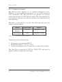
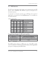
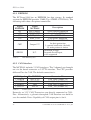
ECUcore-5484
Hardware Manual
PCB Version: 4152.3 (PLD) / 4244.0 (FPGA)
Edition November 2009
system house for distributed automation
ECUcore-5484
Status / Changes
Status: released
Date/ Version
L-1177e_01
L-1177e_02
Section
Change
initial version
FPGA functionality added
Editor
K.Otto
K.Otto
© SYS TEC electronic GmbH 2008 L-1177e_02
ECUcore-5484
In this manual are descriptions for copyrighted products, which are not explicitly
indicated as such. The absence of the trademark ( ) symbol does not infer that a
product is not protected. Additionally, registered patents and trademarks are
similarly not expressly indicated in this manual.
The information in this document has been carefully checked and is believed to be
entirely reliable. However, SYS TEC electronic GmbH assumes no responsibility
for any inaccuracies. SYS TEC electronic GmbH neither gives any guarantee nor
accepts any liability whatsoever for consequential damages resulting from the use
of this manual or its associated product. SYS TEC electronic GmbH reserves the
right to alter the information contained herein without prior notification and
accepts no responsibility for any damages, which might result.
Additionally, SYS TEC electronic GmbH offers no guarantee nor accepts any
liability for damages arising from the improper usage or improper installation of
the hardware or software. SYS TEC electronic GmbH further reserves the right to
alter the layout and/or design of the hardware without prior notification and
accepts no liability for doing so.
Copyright 2009
SYS TEC electronic GmbH. rights – including those of
translation, reprint, broadcast, photomechanical or similar reproduction and
storage or processing in computer systems, in whole or in part – are reserved. No
reproduction may occur without the express written consent from SYS TEC
electronic GmbH.
WORLDWIDE
Address:
SYS TEC electronic GmbH
August-Bebel-Str. 29
D-07973 Greiz
GERMANY
Ordering
+49 (3661) 6279-0
Information: [email protected]
Technical
Support:
+49 (3661) 6279-0
[email protected]
Fax:
+49 (3661) 62 79 99
Web Site:
http://www.systec-electronic.com
2rd Edition November 2009
SYS TEC electronic GmbH 2001
L-1177e_02
3
Index of Figures and Tables
1
2
3
4
5
Introduction......................................................................................... 1
Ordering Information and Support .................................................. 3
Properties of the ECUcore-5484 ........................................................ 5
3.1 Overview ...................................................................................... 5
3.2 Block Diagram ............................................................................. 8
Component Descriptions .................................................................. 11
4.1 Pin-header Connection ............................................................... 11
4.2 Jumper Configuration................................................................. 17
4.3 Power Supply ............................................................................. 19
4.4 Reset Characteristics .................................................................. 20
4.5 Chip Configuration after Reset .................................................. 21
4.6 Memory Interface ....................................................................... 22
4.6.1 SDRAM-Bus ................................................................. 22
4.6.2 Flexbus .......................................................................... 22
4.7 Ethernet Controller..................................................................... 23
4.7.1 MAC Address................................................................ 23
4.8 I2C-Module ................................................................................ 23
4.8.1 Real-Time-Clock........................................................... 24
4.8.2 Temperature Sensor ...................................................... 26
4.9 DSPI-Interface............................................................................ 27
4.9.1 EEPROM....................................................................... 28
4.9.2 CAN Interface ............................................................... 28
4.10 Serial Interface ........................................................................... 29
4.11 DMA controller .......................................................................... 30
4.12 BDM/JTAG Port of MCF5484 .................................................. 31
4.13 CPLD.......................................................................................... 32
4.14 FPGA.......................................................................................... 32
Technical Data................................................................................... 33
SYS TEC electronic GmbH 2008
L-1177e_02
ECUcore-5484
Index of figures and tables
Table 1:
Pinout high density connectors................................................ 13
Table 2:
BDM/JTAG module ................................................................ 14
Table 3:
Signal description .................................................................... 16
Table 4:
Overview of the Solder Jumpers and Default Settings............ 18
Table 5:
I2C Components ...................................................................... 24
Table 6:
Temperature Sensor Address ................................................... 26
Table 7:
SPI Signals............................................................................... 27
Table 8:
EEPROM Signals .................................................................... 28
Table 9:
CAN Signals ............................................................................ 28
Table 10:
UART Signals.......................................................................... 29
Table 11:
Timer Signals ........................................................................... 30
Table 12:
Technical Data ......................................................................... 33
Figure 1:
ECUcore-5484 ........................................................................... 5
Figure 2:
Block Diagram ECUcore-5484.................................................. 8
Figure 3:
Pinout ....................................................................................... 11
Figure 4:
Jumper positions PCB 4152.3 (PLD) ...................................... 17
Figure 5:
Jumper positions PCB 4244.0 (FPGA).................................... 17
Figure 6:
Physical Dimensions................................................................ 33
© SYS TEC electronic GmbH 2008 L-1177e_02
Introduction
1 Introduction
This manual describes the function and technical data for the
ECUcore-5484, but not for the microcontroller Freescale Coldfire
MCF5484 or any other supplemental products. Please refer to the
corresponding manuals and documentation for any other products you
may use.
Low-active signals are denoted by a „/“ in front of the signal name
(i.e. “/RD”). The representation “0” indicates a logical-zero or lowlevel signal. A “1” is the synonym for a logical one or high-level
signal.
L-1177e_02 © SYS TEC electronic GmbH 2008
1
ECUcore-5484
2
© SYS TEC electronic GmbH 2008 L-1177e_02
Ordering Information and Support
2 Ordering Information and Support
Part Number
4001000
4001013
4001015
Version
ECUcore-5484, PLD version
ECUcore-5484, FPGA ECP2-6
ECUcore-5484, FPGA ECP2-20
The ECUcore-5484 standard version (batch module) features:
• Freescale MCF5484 MCU with 200 MHz
• 16MiB FLASH
• 64MiB DDR-SDRAM
• 32kiB EEPROM
• CPLD with 320 macrocells (640LUT's)
alternatively FPGA with 6000 or 21000 LUT's
• Ethernet PHY
• Real-Time-Clock
• Reset-/Watchdog-IC
• Temperature-Sensor
• single power supply 3,3V (all other voltages are derived onboard)
• ESD Handling Instructions (printed version)
You can order a kit with Module and Developmentboard. The Board
will provide you for rapid application development.
It delivers:
• power supply connector 9-24VDC and a external power supply
• some Keys and LED's to test IO-functionality,
• Connectors for all module-interfaces
• USB-Host with 2 Connectors
• Ethernet-Switch to duplicate the second Ethernet-Interface
• Potentiometer with SPI-ADC and a EEPROM to test SPI
• programmable LED-Driver to test I²C
• BDM and JTAG-Interfaces
• Expansion connector for developing user periphery (a simple
IO-Expansion board with 24 keys and 21 LED's is also
available - Ord.No. 4004004)
L-1177e_02 © SYS TEC electronic GmbH 2008
3
ECUcore-5484
Software Support:
• Integrated Development Environment with complete GNU
toolchain for M68k architecture
• colilo bootloader (pre-installed)
• Linux
• plc-firmware
• CANopen protocol stack (limited function, obj-code library)
• CANopen Configuration Suite (Evaluation Version)
• CAN-Report CAN-bus monitor (Evaluation Version)
• OD-Builder
4
© SYS TEC electronic GmbH 2008 L-1177e_02
Properties of the ECUcore-5484
3 Properties of the ECUcore-5484
3.1
Overview
The ECUcore-5484 belongs to the SYS TEC’s ECUcore family. The
ECUcore-5484 integrates all elements of a microcontroller system on
a board. Due to the most modern SMD packages and by the multilayer
design, the module could be manufactured on minimum size.
Figure 1:
ECUcore-5484
L-1177e_02 © SYS TEC electronic GmbH 2008
5
ECUcore-5484
The dimensions of the board are 70mm x 41,5mm and with two
included board connectors it is multifunctional in embedded systems.
The ECUcore-5484 includes a Freescale MCF5484 microcontroller. It
is a highly-integrated 32-bit microprocessors based on the V4-core of
ColdFire microarchitecture.
The interconnection to a baseboard is allowed through a pair of highdensity connectors with summary 240 Pin, .
The ECUcore-5484 offers the following features:
•
Internal Features of the Freescale Coldfire MCF5484:
o internal 200MHz CPU-clock from external 33-66,67MHz
o DDR-/SDR-SDRAM Interface
32kiB Data- / 32kiB Instruction-Cache
o 32bit multiplexed address-data bus "Flexbus" for
connection of flash and other periphery, usable as 16bit
demultiplexed, 6 chip select signals, 33-66MHz,
o PCI bus (only usable at PLD-version)
o 32kiB SRAM
o 2 Fast Ethernet Controller MAC
o 2 FlexCAN 2.0B controllers, each with 16 message
buffers
o I2C
o DMA-SPI with 4 (max. 8) chip selects
o Watchdog Timer
o 2 Periodic Interrupt Timer
o 4 General Purpose Timers
o Interrupt Controller
o 7 external Interrupts (shared with other functionality)
o 16-channel DMA
o GPIO module
o JTAG/BDM module
o 388-pin BGA package
6
© SYS TEC electronic GmbH 2008 L-1177e_02
Properties of the ECUcore-5484
•
Memory Configuration:
o 16MiB Flash-Memory (4-64MiB)
o 64MiB DDR-SDRAM (64-128MiB)
o 32kiB EEPROM (256Byte – 32kiB)
•
Communication features:
o
o
o
o
o
o
•
4 UART as LVTTL
2 CAN as LVTTL
SPI with 8 chip select
I²C-Interface
1 Ethernet interface (PHY onboard)
1 Ethernet interface (only MAC)
Other Board-Level Features:
o CPLD on Flexbus with 640 LUTs and 34 GPIO's
o FPGA on Flexbus with 6000 / 21000 LUT's and
80 GPIO's
o Reset- and Watchdog-IC or Power Sequencer at FPGA
version
o Power failure recognition
o battery buffered real-time-clock
o temperature sensor
o JTAG/BDM module
o 3.3V operating voltage
onboad generated core and ddr-sdram-voltages
o Industrial temperature range (-40°C to +85°C)
o RoHS compliant
L-1177e_02 © SYS TEC electronic GmbH 2008
7
ECUcore-5484
3.2
Block Diagram
Powersupply
50MHz
Oszillator
PLL
Vin = 3.3 V
Vout = 1.5 V
= 2.5 V
= 1.25 V
Temperatursensor
I2C
RTC
SPI
EEPROM
32kByte
2 CAN
ETH0
2 Ethernet
MAC
Coldfire
MCF5484
V4-Core
200 MHz
PHY Micrel
ETH1
GPIOs
4 UARTs
Connector
PCI-Bus*
BDM /
JTAG
/INT
SDRAM-Bus
CPLD/FPGA
GPIO
Flexbus
/FB_CS0
DDR SDRAM
64MiB
addresslatch
NOR FLASH
16MiB
AD[31:0], /FB_CS[5:2]
BWE[3:0], R/W, OE, ALE, TA
Figure 2:
Block Diagram ECUcore-5484
*) CPU-PCI-Bus brought out only at PLD-Version
8
© SYS TEC electronic GmbH 2008 L-1177e_02
Properties of the ECUcore-5484
L-1177e_02 © SYS TEC electronic GmbH 2008
9
Component Descriptions
4 Component Descriptions
The functions of the on-board components are explained in the
following sections.
4.1
Pin-header Connection
The ECUcore-5484 has two board connectors. Each of the SMT pin
header strips consists of 120 contacts divided into double rows. In
total the module has 240 contacts. Separate ground pins in the middle
of the connectors provide a large ground connection.
In addition to the high density connectors a on-module BDM/JTAG
interface of MCF5484 is prepared by pads at the front of the board.
25
23
21
19
17
15
13
11
9
7
5
3
1
1
60
1
60
A
B
1
60
1
60
C
D
Figure 3:
Pinout
The pitch of the board connectors is about 0,5mm. The header
connectors equipped on the ECUcore-5484 are the QTH series
provided by Samtec.
The series mates with Samtec Products socket series QSH,
for example: "QSH-060-01-F-D-A-K". Please refer to the datasheet
and their electrical specifications.
L-1177e_02 © SYS TEC electronic GmbH 2008
11
ECUcore-5484
The columns A and B representing connector 1. In addition the
columns C and D representing connector 2.
The following table defines the pinout.
Signal
Pin
Pin
Signal
Signal
Pin
Pin
Signal
PSTD0
PSTD1
PSTD2
PSTD3
PSTD4
PSTD5
PSTD6
PSTD7
SCL
SDA
PCI_0/IO35
PCI_2/IO37
PCI_4/IO39
PCI_6/IO41
PCI_8/IO43
PCI_10/IO45
PCI_12/IO47
PCI_14/IO49
PCI_16/IO51
PCI_18/IO53
PCI_20/IO55
PCI_22/IO57
PCI_24/IO59
PCI_26/IO61
PCI_28/IO63
PCI_30/IO65
PCI_TRDY/IO67
/PCI_CXBE0/IO69
/PCI_CXBE1/IO71
/PCI_CXBE2/IO73
A01
A02
A03
A04
A05
A06
A07
A08
A09
A10
A11
A12
A13
A14
A15
A16
A17
A18
A19
A20
A21
A22
A23
A24
A25
A26
A27
A28
A29
A30
B01
B02
B03
B04
B05
B06
B07
B08
B09
B10
B11
B12
B13
B14
B15
B16
B17
B18
B19
B20
B21
B22
B23
B24
B25
B26
B27
B28
B29
B30
/RSTI
/MR
/RSTO
/BKPT
PSTCLK
TCK
DSI
DSO
DSCLK
MTMOD0
PCI_1/IO36
PCI_3/IO38
PCI_5/IO40
PCI_7/IO42
PCI_9/IO44
PCI_11/IO46
PCI_13/IO48
PCI_15/IO50
PCI_17/IO52
PCI_19/IO54
PCI_21/IO56
PCI_23/IO58
PCI_25/IO60
PCI_27/IO62
PCI_29/IO64
PCI_31/IO66
/PCI_IRDY/IO68
PCI_PAR/IO70
/PCI_PERR/IO72
/PCI_SERR/IO74
2,5V_EPHY
GND
Eth0_RX+
Eth0_RXGND
Speed
PFEC1L0
PFEC1L1
PFEC1L2
PFEC1L3
PFEC1L4
PFEC1L5
PFEC1L6
PFEC1L7
CAN_Rx0
CAN_Tx0
CAN_Rx1
CAN_Tx1
RxD0
TxD0
RxD1
TxD1
/PSC1_RTS
/PSC1_CTS
SPI_MTSR
SPI_MRST
/SPI_CS2
/SPI_CS4
/SPI_CS6
/FB_BWE0
C01
C02
C03
C04
C05
C06
C07
C08
C09
C10
C11
C12
C13
C14
C15
C16
C17
C18
C19
C20
C21
C22
C23
C24
C25
C26
C27
C28
C29
C30
D01
D02
D03
D04
D05
D06
D07
D08
D09
D10
D11
D12
D13
D14
D15
D16
D17
D18
D19
D20
D21
D22
D23
D24
D25
D26
D27
D28
D29
D30
GND
Eth0_TXEth0_TX+
GND
Link/Act
PFEC1H0
PFEC1H1
PFEC1H2
PFEC1H3
PFEC1H4
PFEC1H5
PFEC1H6
PFEC1H7
E1MDIO
E1MDC
nc/PWR_TDI
nc/PWR_TDO
nc/PWR_TMS
RxD2
TxD2
RxD3
TxD3
/PSC3_RTS
/PSC3_CTS
SPI_CLK
/SPI_CS1
/SPI_CS3
/SPI_CS5
/SPI_CS7
/FB_BWE1
12
© SYS TEC electronic GmbH 2008 L-1177e_02
Component Descriptions
Signal
Pin
Pin
Signal
Signal
Pin
Pin
Signal
/PCI_CXBE3/IO75
PCI_IDSEL/IO77
/PCI_STOP/IO79
/PCI_BG0
/PCI_BG1
/PCI_BG2
/PCI_BG3
/PCI_BG4
FB_AD0
FB_AD2
FB_AD4
FB_AD6
FB_AD8
FB_AD10
FB_AD12
FB_AD14
FB_AD16
FB_AD18
FB_AD20
FB_AD22
FB_AD24
FB_AD26
FB_AD28
FB_AD30
FB_R/W
VBAT
3,3V
3,3V
3,3V
3,3V
A31
A32
A33
A34
A35
A36
A37
A38
A39
A40
A41
A42
A43
A44
A45
A46
A47
A48
A49
A50
A51
A52
A53
A54
A55
A56
A57
A58
A59
A60
B31
B32
B33
B34
B35
B36
B37
B38
B39
B40
B41
B42
B43
B44
B45
B46
B47
B48
B49
B50
B51
B52
B53
B54
B55
B56
B57
B58
B59
B60
/PCI_DEVSEL/IO76
/PCI_FRAME/IO78
/PCI_RESET/IO80
/PCI_BR0
/PCI_BR1
/PCI_BR2
/PCI_BR3
/PCI_BR4
FB_AD1
FB_AD3
FB_AD5
FB_AD7
FB_AD9
FB_AD11
FB_AD13
FB_AD15
FB_AD17
FB_AD19
FB_AD21
FB_AD23
FB_AD25
FB_AD27
FB_AD29
FB_AD31
/FB_OE
3,3V
3,3V
3,3V
3,3V
3,3V
/FB_BWE2
/FB_CS2
/FB_CS4
FB_ALE
/FB_TA
/DACK0
/IRQ5
/IRQ7
TOUT0
TOUT1
TOUT3
IO1
IO3
IO5
IO7
IO9
IO11
IO13
IO15
IO17
IO19
IO21
IO23
IO25
IO27
IO29
IO31
IO33
PLD_TMS
PLD_TCK
C31
C32
C33
C34
C35
C36
C37
C38
C39
C40
C41
C42
C43
C44
C45
C46
C47
C48
C49
C50
C51
C52
C53
C54
C55
C56
C57
C58
C59
C60
D31
D32
D33
D34
D35
D36
D37
D38
D39
D40
D41
D42
D43
D44
D45
D46
D47
D48
D49
D50
D51
D52
D53
D54
D55
D56
D57
D58
D59
D60
/FB_BWE3
/FB_CS3
/FB_CS5
/DREQ0
/BOOT
PFI
/IRQ6
TIN0
TIN1
TIN3
IO0
IO2
IO4
IO6
IO8
IO10
IO12
IO14
IO16
IO18
IO20
IO22
IO24
IO26
IO28
IO30
IO32
IO34
PLD_TDI
PLD_TDO
Table 1:
Pinout high density connectors
When two pin assignments at pin then first is for module with PLD
and second for module with FPGA.
L-1177e_02 © SYS TEC electronic GmbH 2008
13
ECUcore-5484
The following table shows the BDM/JTAG layout with pin names.
Signal
Pin
Pin
Signal
not connected
1
2
/BKPT
GND
3
4
DSCLK
GND
5
6
TCK
/RSTI
7
8
DSI
3,3V
9
10
DSO
GND
11
12
PSTD7
PSTD6
13
14
PSTD5
PSTD4
15
16
PSTD3
PSTD2
17
18
PSTD1
PSTD0
19
20
GND
not connected
21
22
not connected
GND
23
24
PSTCLK
not connected
25
26
/FB_TA
Table 2:
BDM/JTAG module
The following table defines the function of signals. Most modul pins
have the same name like the IC-Pin. So you can find in the relevant
datasheet additional informations about the functionality.
Signal
Function (alternate function)
PSTD0..PSTD7
/BKPT
PSTCLK
TCK
DSI
DSO
DSCLK
BDM/JTAG-Interface of MCF5484
MTMOD0
/RSTI
/MR
/RSTO
SCL
SDA
PCI_0..AD31
PCI_TRDY
/PCI_IRDY
PCI_PAR
/PCI_PERR
/PCI_SERR
/PCI_CXBE0..3
/PCI_DEVSEL
/PCI_FRAME
14
signal to choose between BDM
and JTAG mode
Reset output of
Reset/Watchdog-IC
Manual Reset input of
Reset/Watchdog-IC
Reset output of MCF5484
I²C interface
PCI-Bus
Dir
On-board usage
(only MCF5484signals)
Transmitter
/Receiver
MCF5484
I
I/O
I
O
I/O
I/O
pulldown
(low = BDM mode)
Reset input of CPU,
Flash, PLD, Eth-PHY
pullup
MCF5484
Reset-IC
Reset-IC
MCF5484
Temperature sensor,
RTC
MCF5484
MCF5484
© SYS TEC electronic GmbH 2008 L-1177e_02
Component Descriptions
Signal
Function (alternate function)
Dir
PCI_IDSEL
/PCI_STOP
/PCI_RESET
/PCI_BG0..4
PCI-Bus / GPIO
I/O
/PCI_BR0..4
PCI-Bus / GPIO
I/O
FB_AD0..AD31
FB_R/W
/FB_OE
FB_ALE
/FB_BWE0..3
/FB_CS2..5
/FB_TA
Flexbus address/data
Flexbus read/write
Flexbus output enable
Flexbus address latch enable
Flexbus byte write enable
Flexbus chip select
Flexbus transfer acknowledge
I/O
O
O
O
O
O
I
Eth0_TX+, TXEth0_RX+, RX2,5V_EPHY
Link/Act "LED0"
Speed "LED1"
Ethernet interface0 (PHY)
O
I
O
O
O
PFEC1L0..7
PFEC1H0..7
E1MDIO
E1MDC
Common voltage of interface0
Link/Act Indicator interface 0
Speed Indicator interface 0
Ethernet Interface 1 (MAC)
MII- or 7Wire-Interface /
GPIO
Ethernet Interface 1
Ethernet Interface 1
On-board usage
(only MCF5484signals)
Transmitter
/Receiver
MCF5484
/PCI_BR4 is default
used as /INT-signal
from PLD to CPU
MCF5484
Flash, PLD
MCF5484
onboard LED
Ethernet PHY
Micrel
KS8721BL
IO
MCF5484
I/O
O
nc
no function (faulty USB Device
interface)
I/O
MCF5484
CAN_Rx0, Rx1
CAN_Tx0, Tx1
CAN-Interface
LVTTL-Level
I
O
MCF5484
RxD0..3
TxD0..3
UART0..3
LVTTL-Level
I
O
MCF5484
/PSC1_RTS
/PSC1_CTS
handshake signals of UART1 /
GPIO
/PSC3_RTS
/PSC3_CTS
handshake signals of UART3 /
GPIO
SPI_MTSR
SPI_MRST
SPI_CLK
/SPI1..7
DSPI interface
/PFI
signal on /DACK1 to determine the
boot-sequence (to colilo or Linux)
power fail input of reset-ic
/DREQ0, /DACK0
DMA controller / GPIO
/BOOT
L-1177e_02 © SYS TEC electronic GmbH 2008
I/O
onboard pullup 4,7k
and Switch 1-1 to GND
MCF5484
I/O
MCF5484
O
/CS demux ICr
I
pullup (4,7k) and switch
(S1-2) to GND
pullup 4,7k to 3,3V
MCF5484
Reset-IC
I/O
15
ECUcore-5484
Signal
Function (alternate function)
Dir
On-board usage
(only MCF5484signals)
Transmitter
/Receiver
/IRQ7
/IRQ6, 5
Interrupt input (NMI)
Interrupt input / GPIO
I
I/O
pullup 4,7k
MCF5484
TIN0..1
TIN2..3
TOUT0..1
TOUT2..3
Timer input
Timer input / GPIO
Timer output
Timer output / GPIO
I
I/O
O
I/O
IO0..80
GPIO
(depends on pld-configuration)
I/O
PLD_TMS
PLD_TCK
PLD_TDI
PLD_TDO
PLD JTAG interface
PWR_TMS
PWR_TDI
PWR_TDO
PowerSequencer
JTAG interface
VBAT
3,3V
Buffer supply for RTC (3,3V)
power supply of module
Table 3:
16
MCF5484
PLD
I
I
RTC
Signal description
© SYS TEC electronic GmbH 2008 L-1177e_02
Component Descriptions
4.2
Jumper Configuration
On default the jumpers are configuered for a prperly function of
module. Change positions only if you really need it in a special
application ! Read user manual of MCF5484 for the boot and resetconfiguration before you change the configuration jumpers J1-J6 !
The following figure shows the positions of jumpers. All placed on
top-side of module.
J201
J17
Pin1
J6
J5
J4
J3
J2
J1
Pin1
Pin1
J7
ON
S1
Figure 4:
Pin1
1 2
J8
Jumper positions PCB 4152.3 (PLD)
J6
J5
J4
J3
J2
J1
R453
J17
Pin1
Pin1
J7
S1
1 2
Pin1
J8
Figure 5:
Jumper positions PCB 4244.0 (FPGA)
L-1177e_02 © SYS TEC electronic GmbH 2008
17
ECUcore-5484
The function of S1 depence on application. Read the manual of
software for further informations.
The following table lists each solder jumper and its function on the
ECUcore-5484.
Jumper
Jumper Pad
Setting
2-3 (default)
J1
1-2
2-3 (default)
J2
1-2
1-2 default
J3
2-3
2-3/1-2/1-2 (default)
J4/J5/J6
Signal
FB_AD2
FB_AD3
FB_AD5
FB_AD9/10/11
other
J7/J8
2-3/2-3
MTMOD0
1-2
J201
(PLD module only)
18
/PSC1_CTS
2-3 default
J17
Table 4:
1-2/1-2 (default)
1-2 (default)
2-3
EEPROM-/WP
PLD_IRQ
Function
FB_CS0 enable autoacknowledge
disable
BWE/BE configured as /BWE
BWE/BE configured as /BE
BWE/BE3..0 used as BWE/BE
BWE/BE3..2 used as TSIZ1..0
BWE/BE1..0 used as FB_AD1..0
together with AD8=1 and AD12=0
FB_AD12..8 = 00011 =
ext.50MHz , int. 100MHz, core 200MHz
not possible with the oscillator
S1-1 switches /PSC1_CTS (onboard
pullup) to GND
S1-1 switches MTMOD0 (onboard
pulldown) to 3,3V
read/write operations are possible
depence on WPEN-Bit write operations
are inhibited
/IRQ-signal of PLD is connected to
/PCI_BR4 (=/INT4 of CPU)
connected to TIN3 (=/INT3 of CPU)
Overview of the Solder Jumpers and Default Settings
© SYS TEC electronic GmbH 2008 L-1177e_02
Component Descriptions
4.3
Power Supply
The ECUcore-5484 must be supplied with an input voltage of
+3.3VDC. The typical current consumption is approximately 600mA.
The 3,3V supplys directly:
• MCF5484 IO voltage
• CPLD/FPGA
• Flash
• RTC, Temperaturesensor, EEPROM
• Logic
So be carefully and provide a good voltage with low tolerance and low
ripple. See "Technical Data" for detailed informations.
The rise time of power on ramp of 3,3V should be slower than 1µs
(for MCF5484) and faster than 30ms (CPLD-requirement).
The onboard switching regulators generate all the other needed
voltages. These are:
• 1,5V for MCF5484 core, core-pll, usb-pll supply
• 2,5V for DDR-SDRAM supply
• 1,25V for DDR-SDRAM reference
• 1,2V for FPGA Core supply
A Reset-IC watches the voltages 2,5V and 1,5V and reset's the board
if one voltage dropes below 0,7V. The 3,3V will be watched too, and a
reset is occured if this voltage dropes below 3,08V.
For FPGA a PowerSequencer is needed. It watch all voltages and
realized the power on sequence for FPGA. Other functions are reset,
watchdog and power fail function.
L-1177e_02 © SYS TEC electronic GmbH 2008
19
ECUcore-5484
4.4
Reset Characteristics
Basically the reset characteristics are defined by the EXAR
Supervisory Circuit SP706T, which is responsible for generating the
system reset signal /RSTI. For FPGA-version the functionality of
reset-ic is implemented in power-sequencer.
The reset in signal (/RSTI) is low-active and connected to a pull-up
resistor. It is asserted by the following parameters:
•
•
•
Power Supply Voltage VCC drops below 3.08V
Manual Reset (/MR) voltage drops below 0.6V
WDI pin: no signal shift occurs within a timespan of 1.6s
An internal timer releases /RESET after 200ms. When a brownout
condition occurs in the middle of a previously initiated reset pulse, the
pulse continues for at least another 140ms. As soon as reset is released
and WDI is driven HIGH or LOW, the timer will start counting.
Pulses with a minimum pulse width of 50ns can be detected.
The Reset-IC has a build in watchdog timer. During reset the
watchdog timer will stay cleared and will not count. It will started
when the coldfire-pin /PSC0_RTS (used as watchdog trigger) left the
tristate-state and drives a high or low. Then this pin must toggle into
1,6sec. to trigger the watchdog. The output is coupled with /RSTI by
Diodes.
The Power Fail Input signal (PFI) is connected to PFI-input of ResetIC with an 4,7k pullup. It can be switched externaly by open-collector
or LVTTL output. The detection of power fail should be near the
power supply input of the device (e.g. the 24VDC supply). So you can
use a longer time to save critical data or send messages about the
error.
To connect the signal /PFO of Reset-IC to external interrupt /INT6
close the soldering jumper R408 (R453 on FPGA version) with 0R.
Default the Resistor is open and the /INT6 can used as GPIO or for
other interrupt sources. You can find the resistor-pads at Pin 5 of
SP706T on the bottom side of module.
20
© SYS TEC electronic GmbH 2008 L-1177e_02
Component Descriptions
4.5
Chip Configuration after Reset
The Chip Configuration will be read on Flexbus-pins at reset
FB_AD12..FB_AD0. Don't drive this signale by external IC's during
the reset-state. Generaly make shure that the bus devices only drives if
her chip-select is activated by Coldfire.
See Chapter "Jumper Configuration" Table "Overview of the Solder
Jumpers and Default Settings" for default configuration. Jumpers are
mounted with 4,7k-Resistors.
The configuration is chose to support the onboard Flash and PLD with
following features:
• portsize for /CS0 (Flash) is 16Bit
• autoacknowledge for /CS0 is enabled
• BWE3..0 of /CS0 is only asserted for write cycles
• Flexbus is used for both address and data
(PCIbus can completely used separate)
• /BE/BWE3..0 is used as byte/byte write enable
• clock ratio is configured for external 50MHz oszillator, internal
100MHz clock and core 200 MHz clock
L-1177e_02 © SYS TEC electronic GmbH 2008
21
ECUcore-5484
4.6
Memory Interface
The external memory interface of the MCF-5484 is divided into
external SDRAM and Flexbus. For data storage a eeprom is used
connected to SPI-bus.
External SDRAM and Flexbus are 2 separate bus-systems with
different portpins on MCF5484. Flexbus is used onboard for Flash and
PLD an accessible on board-connector. SDRAM-bus is only used
onboard.
4.6.1 SDRAM-Bus
The SDRAM-bus supports SDR-SDRAM and DDR-SDRAM.
Onboard two 16bit DDR-SDRAM's mounted, accessible as one 32bitdevice. Addressing is realized with /SD_CS0. Default RAM-Types are
"Micron MT46V16M16BG-75" or compatible with 32MiB each and
7,5ns cycle time.
4.6.2 Flexbus
Flash-Memory:
Flexbus is connected to Flash via address latch for demultiplexed
address bus. One Flash-IC with 16bit data-bus is mounted.
Default Flash-Type is "Spansion S29GL128N10" with 16MiB and
100ns cycle time.
Used Flexbus control signals: /FB_CS0, /FB_OE, FB_R/W, FB_ALE
PLD/FPGA:
For fast accessing the PLD the flexbus is using too. The complete
address/data bus pins of MCF5484 are connected to PLD.
Demultiplexing can be effect in PLD.
Used Flexbus control signals: /FB_CS1, /FB_OE, FB_R/W, FB_ALE
22
© SYS TEC electronic GmbH 2008 L-1177e_02
Component Descriptions
4.7
Ethernet Controller
The MCF5484 supports two 10/100 Ethernet channels by internal
MAC with MII-interface.
For the first channel a on-board PHY chip KSZ8721BLI from Micrel
realized a 10/100 physical interface.
Board connector signals are:
Signal
description
Eth0_Tx+
Tx+ from PHY
Eth0_TxTx- from PHY
Eth0_Rx+
Rx+ from PHY
Eth0_RxRx- from PHY
2V5_EPHY
2,5V PHY-Supply
Link/Act
output for LED (parallel a yellow LED
is mounted on board with 270R)
Speed
output for LED
Tx and Rx Signals are pulled up with 49,9R to 2,5V-EPHY.
The second MII-interface is brought out to board connector.
The MII-Interfaces defaults to GPIO after reset. The GPIO module
must be configured to enable the peripheral function of the appropriate
pins prior to configuring the Fast Ethernet Controller.
4.7.1 MAC Address
SYS TEC electronic has aquired a pool of these MAC addresses. The
MAC address for the first Ethernet-Interface Eth0 is barcode-labelled
attached on the ECUcore-5484.
4.8
I2C-Module
The ECUcore-5484 features one I2C interface, a 2-wire serial bus
used for communication with I2C devices. The bus is brought out via
the board connector. The ECUcore-5484 comes with two on-board
I2C devices. Please refer to the table below.
L-1177e_02 © SYS TEC electronic GmbH 2008
23
ECUcore-5484
I2C device
Real-Time-Clock Epson 8564JE
(U201)
Temperature Sensor TI TMP101
(U202)
Table 5:
Address
0xA2
0x90 (default)
0x92 upon request
I2C Components
The I2C-Module defaults to GPIO after reset. The GPIO module must
be configured to enable the peripheral function of the appropriate pins
prior to configuring the I2C-Module.
4.8.1 Real-Time-Clock
The ECUcore-5484 is equipped with a Real-Time-Clock to manage
real-time application. The device offers functions such as calendar
clock, alarm and timer. It also outputs pre-defined frequencies
(32.768kHz, 1024Hz, 32Hz, 1Hz) via the CLKOUT pin.
RTC Characteristics:
•
•
•
Built-in crystal running at 32768Hz
programmable alarm, timer and interrupt functions
low power consumption:
o Bus active:
o Bus inactive, CLKOUT inactive:
1mA
1µA
The Real-Time-Clock is supplied by 3.3V DC. If the system voltage
crashes, the backup battery supplies the RTC (if connected!).
Device Address:
•
•
24
0xA2 when write mode
0xA3 when read mode
© SYS TEC electronic GmbH 2008 L-1177e_02
Component Descriptions
The Pin CLKOE is pulled high. So the clock output can be enabled by
setting the bit 'FE' in Register 'Clock Out frequency' to 1.
One of the output-pins of RTC can connect to CPU-pin
'/DREQ1_/IRQ1'.
resistor
function (when R equipped)
R15 (default equipped) CLKOUT is connected to /IRQ1
R16 (default open)
/RTC_INT is connected to /IRQ1
At module with FPGA both signals are connected to FPGA-Pins and
can be used in Software.
L-1177e_02 © SYS TEC electronic GmbH 2008
25
ECUcore-5484
4.8.2 Temperature Sensor
The ECUcore-5484 disposes of an optional temperature sensor
TMP101 to record ambient temperatures to, e.g, enable protection
from overheating. The ECUcore-5484 just provides the physical
connection between the CPU and the sensor. The communication or
any protective measures are software functions to be provided by the
user application.
The address is adjustable by a resisitor. The following table shows the
various assembly options.
resistor
equipped
(default)
not equipped
(upon request)
Table 6:
ADD0 signal
Address
0 (GND)
1001000x = 0x90
float
1001001x = 0x92
Temperature Sensor Address
Temperature sensor characteristics:
•
•
•
Temperature resolution of 0.0625°C
Temperature range of -55°C to +125°C
Alert pin as interrupt source if temperature exceeds defined limits
The Alert-Pin is connected to CPU-Pin '/PSC0_CTS' and must be
polled to indicate temperature-exceedings.
26
© SYS TEC electronic GmbH 2008 L-1177e_02
Component Descriptions
4.9
DSPI-Interface
The ECUcore-5484 allows high-speed serial communication with SPI
devices such as EEPROM. The DSPI bus signals are brought out via
the board connector.
An onboard 3-to-8 decoder provides up to 8 SPI chip select signals of
which one is reserved for use with EEPROM and 7 are available via
the board connector.
Addressed-decoding:
DSPI_CS pins of CPU
CS0 CS2 CS3 CS5
0
0
0
1
0
0
0
0
1
0
0
0
0
1
0
0
1
1
0
0
0
0
1
0
1
0
1
0
1
1
0
0
1
1
1
0
decoder chipselect
low activ
no chip select
/CS-EEPROM
/SPI_CS1
/SPI_CS2
/SPI_CS3
/SPI_CS4
/SPI_CS5
/SPI_CS6
/SPI_CS7
The following table shows the SPI signals available.
SPI signal (on CPU)
Description
/SPI_CS1-7
Chip Select's on connector
SPI_MTSR (SOUT)
Master Transmit Slave Receive
SPI_MRST (SIN)
Master Receive Slave Transmit
SPI_CLK (SCK)
Clock
Table 7:
SPI Signals
The DSPI module defaults to GPIO after reset. The GPIO module
must be configured to enable the peripheral function of the appropriate
pins prior to configuring the DSPI module.
L-1177e_02 © SYS TEC electronic GmbH 2008
27
ECUcore-5484
4.9.1 EEPROM
The ECUcore-5484 has an EEPROM for data storage. In standard
version the EEPROM provides 32kiB (Typ ATMEL AT25256A). The
following table shows the pinout connection.
Signal
EEPROM
SO
SI
SCK
/CS
Signal
MCF5484
PSPI_MRST
PSPI_MTSR
PSPI_CLK
PSPI_/CS0
/WP
Jumper J17
/HOLD
N.C.
Table 8:
Description
Serial Output EEPROM
Serial Input EEPROM
Clock EEPROM
Chip Select EEPROM
Write Protect EEPROM
for data protection
1: normal read/write (default)
0: write protect is active
connected to high,
Suspends Serial Input,
is not supported
EEPROM Signals
4.9.2 CAN Interface
The MCF5484 includes 2 CAN interfaces. The 2 channels are brought
out via the board connector as LVTTL-interface. The CPU provides
different Pins for CAN. The default connection is:
CAN-Signal
CANRX0
CANTX0
CANRX1
CANTX1
Table 9:
Pin MCF5484
/PSC2CTS
/PSC2RTS
TIN2
TOUT2
Connector-Pin
CAN_Rx0 (X400/C15)
CAN_Tx0 (X400/C16)
CAN_Rx1 (C400/C17)
CAN_Tx1 (X400/C18)
CAN Signals
Externaly an 3,3V CAN-Transceiver can directly connected to CANPins. Alternatively a galvanic decoupled CAN-Interface can build to
save the module. Drive Capability of CAN output pins is 8mA.
28
© SYS TEC electronic GmbH 2008 L-1177e_02
Component Descriptions
4.10 Serial Interface
The ECUcore-5484 supports up to 4 independent UARTs available on
the board connector. They are used to interface serial communication
via RS232 or RS485 level signals. Each interface has two handshakesignals (RTS/CTS), but not all are supported on module. The
following table shows the pinout. Signals are LVTTL. However, the
board does not provide any transceiver.
Signal
MCF5484
PSC0TXD
PSC0RXD
/PSC0CTS
Signal
Connector
TxD0
RxD0
N.C.
N.C.
/PSC0RTS
PSC1TXD
PSC1RXD
/PSC1CTS
/PSC1RTS
PSC2TXD
PSC2RXD
/PSC2CTS
/PSC2RTS
PSC3TXD
PSC3RXD
/PSC3CTS
/PSC3RTS
Table 10:
TxD1
RxD1
PSC_IO2
PSC_IO3
TxD2
RxD2
CAN_Tx0
CAN_Rx0
TxD3
RxD3
PSC_IO6
PSC_IO7
Comment
used as WDI for onboard
Watchdog-IC
used for Temperature-Sensor
INT-Pin
used as second Boot-Signal with
pullup (4k7) and DIP-Switch 2
to GND (s.a. Jumper J8)
when CAN0 not needed
this Pins can be used for
PSC2-Handshake
GPIO's can be used for
PSC3-Handshake
UART Signals
The UART-Modules default to GPIO after reset. The GPIO module
must be configured to enable the peripheral function of the appropriate
pins prior to configuring the UART module.
L-1177e_02 © SYS TEC electronic GmbH 2008
29
ECUcore-5484
4.11 DMA controller
There are two external DMA-Interfaces on MCF5484 consist of
DMA-acknowledge-Pin and DMA-request-Pin. Only one interface is
provided by module as default.
Signal
MCF5484
/DREQ0
/DACK0
Signal
Connector
/DREQ0
/DACK0
/DREQ1
/IRQ1
/DACK1
/BOOT
Table 11:
comment
default onboard connected to
RTC-CLKOUT via 0R-Resistor
or to FPGA
onboard connected to Boot-Switch
(DIP-Switch 1) with pullup 4k7
Timer Signals
To find more informations about DMA as Communication Subsystem
see the user manual of MCF5484.
30
© SYS TEC electronic GmbH 2008 L-1177e_02
Component Descriptions
4.12 BDM/JTAG Port of MCF5484
The ECUcore-5484 provides a BDM/JTAG interface for the CPU
MCF5484. This is for debugging on low level software and
programming the CPU of raw module. In default the module will
distributed with a bootloader to download software over ethernet or
RS232.
BDM/JTAG is accsessible over board connector.
The ECUcore-5484 has a specific BDM/JTAG pinout on the short side
of the board. Here a debug-adapter (e.g. BDM Adapter from P&EMicrocomputer Systems) can directly be plugged. So you can get a
debug-module for target environment, without BDM-connectors on
baseboard.
The function BDM or JTAG is selectable with Signal MTMOD0 on
board-connector or on DIP-SW1 (not default, see description J7/J8).
The MTMOD0-Pin has a 4k7 pulldown on board.
MTMOD0
0 (default)
1
function
normal and Background Debug Mode (BDM)
normal and JTAG mode
Some of the BDM/JTAG Pins has a 4,7k pullup or pulldown resistor
on board:
resistor
signal
pullup
/BKPT, DSI, DSO, DSCLK
pulldown
TCK
L-1177e_02 © SYS TEC electronic GmbH 2008
31
ECUcore-5484
4.13 CPLD
A second JTAG-Port is brought out on the board connector for
programming the CPLD. All Pins has on bord 10k pullup or pulldown
resistors.
resistor
pullup
pulldown
signal
PLD_TDI, PLD_TDO, PLD_TMS
PLD_TCK
PLD-JTAG-signals are onboard connect to MCF5484. So Modules
with Linux supports programming of CPLD from CPU and don't need
external programming devices for PLD.
The Lattice CPLD Type MachXO640 with speed grade '-3' is used.
4.14 FPGA
FPGA is used to provide more functionality. There are more IO-Pin's
and Gates in the FPGA for more flexibilty. This make it possible e.g.
to realize more than one 32bit counter-inputs and pulse-outputs.
The PCI pins at connector would changed in FPGA-IO-Pins. So there
are 80 FPGA-IO's for various functions.
SPI /CS-generation like chapter 4.9 is implemented in FPGA.
SPI-MRST, MTSR and CLK are connected to the FPGA too. So it can
be assigned to any othe IO-Pin. Other way is to implement a external
SPI-unit in FPGA to release the cpu from SPI-communication.
For faster signal handling the cpu-interrupt-pins IRQ1, 3, 4 and 6 are
connected to FPGA.
The Lattice Type "LFE2-6SE-5FN256I" or "LFE2-20SE-6FN256I"
are used.
Programming of FPGA is the same like PLD.
32
© SYS TEC electronic GmbH 2008 L-1177e_02
Technical Data
5 Technical Data
The physical dimensions of the ECUcore-5484 are shown in the figure
below.
41.5mm
2.5mm
2.5mm
70mm
35.05mm
2.5mm
36.9mm
4.55mm
ECUcore-5484
2.5mm
31.05mm
Figure 6:
Physical Dimensions
The height including board connector and components is about 9mm.
The thickness of the PCB is about 1.6mm. The maximum component
height on top is about 2,55mm.
dimensions
weight
operating temperature
storage temperature
operating voltage
current consumption
I/O-Level
Table 12:
70mm x 36,9mm x 7,8mm
approximately 21g
-40°C to +85°C
-40°C to +85°C
+3.3V DC ± 5%
typ. 600mA
+3.3V DC ± 5%
Technical Data
L-1177e_02 © SYS TEC electronic GmbH 2008
33
ECUcore-5484
34
© SYS TEC electronic GmbH 2008 L-1177e_02
Suggestions for Improvement
Document:
Document number:
Hardware Manual ECUcore-5484
L-1177e_02, Edition November 2009
How would you improve this manual?
Did you find any mistakes in this manual?
Submitted by:
Customer number:
Name:
Company:
Address:
Return to:
SYS TEC electronic GmbH
August-Bebel-Str. 29
D-07973 Greiz
GERMANY
Fax : +49 (0) 36 61 / 62 79 99
L-1177e_02 © SYS TEC electronic GmbH 2008
page
Published by
© SYS TEC electronic GmbH 2008
Ord. No. L-1177e_02
Printed in Germany