1
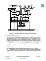
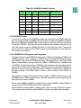
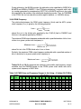
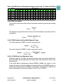
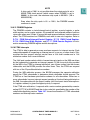
SECTION 10
CONFIGURABLE TIMER MODULE 4
This section is an overview of CTM4 function. Refer to the CTM Reference Manual
(CTMRM/AD) for a comprehensive discussion of CTM capabilities.
10.1 General
The configurable timer module 4 (CTM4) consists of several submodules which are
located on either side of the CTM4 internal submodule bus (SMB). All data and control
signals within the CTM4 are passed over this bus. The SMB is connected to the outside world via the bus interface unit submodule (BIUSM), which is connected to the
intermodule bus (IMB), and subsequently the CPU32. This configuration allows the
CPU32 to access the data and control registers in each CTM4 submodule on the SMB.
Three time base buses (TBB1, TBB2 and TBB4), each 16-bits wide, are used to transfer timing information from counters to action submodules. Figure 10-1 shows a block
diagram of the CTM4.
PCLK1 (fsys ÷ 2 or fsys ÷ 3)
TIME BASE BUS 1 (TBB1)
PULSE WIDTH MODULATION
SUBMODULE (PWMSM8)
CPWM8
PULSE WIDTH MODULATION
SUBMODULE (PWMSM7)
CPWM7
PULSE WIDTH MODULATION
SUBMODULE (PWMSM6)
CPWM6
PULSE WIDTH MODULATION
SUBMODULE (PWMSM5)
CPWM5
DOUBLE ACTION
SUBMODULE (DASM10)
CTD10
DOUBLE ACTION
SUBMODULE (DASM9)
CTD9
CLOCK PRESCALER
SUBMODULE (CPSM)
BUS INTERFACE UNIT
SUBMODULE (BIUSM)
LOAD
MODULUS COUNTER
SUBMODULE (MCSM11)
FREE-RUNNING
COUNTER
SUBMODULE (FCSM12)
MODULUS COUNTER
SUBMODULE (MCSM2)
TIME BASE BUS 4 (TBB4)
TIME BASE BUS 2 (TBB2)
DOUBLE ACTION
SUBMODULE (DASM4)
CTD4
DOUBLE ACTION
SUBMODULE (DASM3)
CTD3
EXTERNAL CLOCK
CTM2C
GLOBAL TIME BASE BUS A
GLOBAL TIME BASE BUS B
CTM4 BLOC
Figure 10-1 CTM4 Block Diagram
MC68336/376
USER’S MANUAL
CONFIGURABLE TIMER MODULE 4
Rev. 15 Oct 2000
MOTOROLA
10-1
The time base buses originate in a counter submodule and are used by the action submodules. Two time base buses are accessible to each submodule.
The bus interface unit submodule (BIUSM) allows all the CTM4 submodules to pass
data to and from the IMB via the submodule bus (SMB).
The counter prescaler submodule (CPSM) generates six different clock frequencies
which can be used by any counter submodule. This submodule is contained within the
BIUSM.
The free-running counter submodule (FCSM) has a 16-bit up counter with an associated clock source selector, selectable time-base bus drivers, writable control registers,
readable status bits, and interrupt logic.The CTM4 has one FCSM.
The modulus counter submodule (MCSM) is an enhanced FCSM. A modulus register
gives the additional flexibility of recycling the counter at a count other than 64K clock
cycles. The CTM4 has two MCSMs.
The double-action submodule (DASM) provides two 16-bit input capture or two 16-bit
output compare functions that can occur automatically without software intervention.
The CTM4 has four DASMs.
The pulse width modulation submodule (PWMSM) can generate pulse width
modulated signals over a wide range of frequencies, independently of other CTM output signals. PWMSMs are not affected by time base bus activity. The CTM4 has four
PWMSMs.
10.2 Address Map
The CTM4 address map occupies 256 bytes from address $YFF400 to $YFF4FF. All
CTM4 registers are accessible only when the CPU32 is in supervisor mode. All
reserved addresses return zero when read, and writes have no effect. Refer to D.7
Configurable Timer Module 4 for information concerning CTM4 address map and
register bit/field descriptions.
10.3 Time Base Bus System
The CTM4 time base bus system is composed of three 16-bit buses: TBB1, TBB2, and
TBB4. These buses are used to transfer timing information from the counter submodules to the action submodules. Two time base buses are available to each submodule.
A counter submodule can drive one of the two time base buses to which it is connected. Each action submodule can choose one of the two time base buses to which
it is connected as its time base. Control bits within each CTM4 submodule select connection to the appropriate time base bus.
The time base buses are precharge/discharge type buses with wired-OR capability.
Therefore, no hardware damage occurs when more than one counter drives the same
bus at the same time.
MC68336/376
USER’S MANUAL
CONFIGURABLE TIMER MODULE 4
Rev. 15 Oct 2000
MOTOROLA
10-2
In the CTM4, TBB2 is global and accessible to every submodule. TBB1 and TBB4 are
split to form two local time base buses. Table 10-1 shows which time base buses are
available to each CTM4 submodule.
Table 10-1 CTM4 Time Base Bus Allocation
Global/Local Time Base
Bus Allocation
Submodule
Global Bus A
Global/Local Time Base
Bus Allocation
Global Bus B
Submodule
Global Bus A
Global Bus B
DASM9
TBB1
TBB2
MCSM 2
TBB4
TBB2
DASM10
TBB1
TBB2
DASM 3
TBB4
TBB2
MCSM 11
TBB1
TBB2
DASM 4
TBB4
TBB2
FCSM 12
TBB1
TBB2
Each PWMSM has an independent 16-bit counter and 8-bit prescaler clocked by the
PCLK1 signal, which is generated by the CPSM. The PWMSMs are not connected to
any of the time base buses. Refer to 10.9 Pulse-Width Modulation Submodule
(PWMSM) for more information.
10.4 Bus Interface Unit Submodule (BIUSM)
The BIUSM connects the SMB to the IMB and allows the CTM4 submodules to communicate with the CPU32. The BIUSM also communicates CTM4 submodule interrupt
requests to the IMB, and transfers the interrupt level, arbitration number and vector
number to the CPU32 during the interrupt acknowledge cycle.
10.4.1 STOP Effect On the BIUSM
When the CPU32 STOP instruction is executed, only the CPU32 is stopped; the CTM4
continues to operate as normal.
10.4.2 Freeze Effect On the BIUSM
CTM4 response to assertion of the IMB FREEZE signal is controlled by the FRZ bit in
the BIUSM configuration register (BIUMCR). Since the BIUSM propagates FREEZE
to the CTM4 submodules via the SMB, the setting of FRZ affects all CTM4
submodules.
If the IMB FREEZE signal is asserted and FRZ = 1, all CTM4 submodules freeze. The
following conditions apply when the CTM4 is frozen:
• All submodule registers can still be accessed.
• The CPSM, FCSM, MCSM, and PWMSM counters stop counting.
• The IN status bit still reflects the state of the FCSM external clock input pin.
• The IN2 status bit still reflects the state of the MCSM external clock input pin, and
the IN1 status bit still reflects the state of the MCSM modulus load input pin.
• DASM capture and compare functions are disabled.
• The DASM IN status bit still reflects the state of its associated pin in the DIS,
IPWM, IPM, and IC modes. In the OCB, OCAB, and OPWM modes, IN reflects
the state of the DASM output flip flop.
MC68336/376
USER’S MANUAL
CONFIGURABLE TIMER MODULE 4
Rev. 15 Oct 2000
MOTOROLA
10-3
• When configured for OCB, OCAB, or OPWM modes, the state of the DASM
output flip-flop will remain unchanged.
• The state of the PWMSM output flip-flop will remain unchanged.
If the IMB FREEZE signal is asserted and FRZ = 0, the freeze condition is ignored, and
all CTM4 submodules will continue to operate normally.
10.4.3 LPSTOP Effect on the BIUSM
When the CPU32 LPSTOP instruction is executed, the system clock is stopped. All
dependent modules, including the CTM4, are shut down until low-power STOP mode
is exited.
10.4.4 BIUSM Registers
The BIUSM contains a module configuration register, a time base register, and a test
register. The BIUSM register block occupies the first four register locations in the
CTM4 register space. All unused bits and reserved address locations return zero when
read. Writes to unused bits and reserved address locations have no effect. Refer to
D.7.1 BIU Module Configuration Register, D.7.2 BIUSM Test Configuration Register, and D.7.3 BIUSM Time Base Register for information concerning BIUSM
register and bit descriptions.
10.5 Counter Prescaler Submodule (CPSM)
The counter prescaler submodule (CPSM) is a programmable divider system that provides the CTM4 counters with a choice of six clock signals (PCLK[1:6]) derived from
the main MCU system clock. Five of these frequencies are derived from a fixed divider
chain. The divide ratio of the last clock frequency is software selectable from a choice
of four divide ratios.
The CPSM is part of the BIUSM. Figure 10-2 shows a block diagram of the CPSM.
MC68336/376
USER’S MANUAL
CONFIGURABLE TIMER MODULE 4
Rev. 15 Oct 2000
MOTOROLA
10-4
fsys
FIRST CPSM
PRESCALER
PCLK1 =
fsys÷ 2
fsys÷ 3
÷2 OR ÷3
8-BIT
PRESCALER
÷2
PCLK2 =
fsys÷ 4
fsys÷ 6
÷4
PCLK3 =
fsys ÷ 8
fsys÷ 12
÷8
PCLK4 =
fsys÷ 16
fsys÷ 24
÷16
PCLK5 =
fsys÷ 32
fsys÷ 48
PCLK6 =
fsys÷ 64
fsys ÷ 128
fsys ÷ 256
fsys÷ 512
fsys ÷ 96
fsys ÷ 192
fsys÷ 384
fsys÷ 768
DIV23 = ÷ 2
DIV23 = ÷ 3
÷32
÷64
÷128
SELECT
÷256
PRUN
DIV23 PSEL1
PSEL0 CPCR
CTM CPSM BLOCK
Figure 10-2 CPSM Block Diagram
10.5.1 CPSM Registers
The CPSM contains a control register (CPCR) and a test register (CPTR). All unused
bits and reserved address locations return zero when read. Writes to unused bits and
reserved address locations have no effect. Refer to D.7.4 CPSM Control Register
and D.7.5 CPSM Test Register for information concerning CPSM register and bit
descriptions.
10.6 Free-Running Counter Submodule (FCSM)
The free-running counter submodule (FCSM) has a 16-bit up counter with an associated clock source selector, selectable time-base bus drivers, control registers, status
bits, and interrupt logic. When the 16-bit up counter overflows from $FFFF to $0000,
an optional overflow interrupt request can be generated. The current state of the 16bit counter is the primary output of the counter submodules. The user can select which,
if any, time base bus is to be driven by the 16-bit counter. A software control register
selects whether the clock input to the counter is one of the taps from the prescaler or
an input pin. The polarity of the external input pin is also programmable.
In order to count, the FCSM requires the CPSM clock signals to be present. After
reset, the FCSM does not count until the prescaler in the CPSM starts running (when
the software sets the PRUN bit). This allows all counters in the CTM4 submodules to
be synchronized.
The CTM4 has one FCSM. Figure 10-3 shows a block diagram of the FCSM.
MC68336/376
USER’S MANUAL
CONFIGURABLE TIMER MODULE 4
Rev. 15 Oct 2000
MOTOROLA
10-5
TBBA
Time base buses
TBBB
6 clocks (PCLK[1:6]) from prescaler
Bus
select
DRVADRVB
Control register bits
INPUT pin
CTM2C
Clock
select
Edge
detect
IN
Overflow
16-bit
up counter
CLK2 CLK1 CLK0
Control register bits
COF
IL2
IL1
Interrupt
control
IL0 IARB3
Control register bits
Submodule bus
CTM FCSM BLOCK
Figure 10-3 FCSM Block Diagram
10.6.1 FCSM Counter
The FCSM counter consists of a 16-bit register and a 16-bit up-counter. Reading the
register transfers the contents of the counter to the data bus, while a write to the
register loads the counter with a new value. Overflow of the counter is defined to be
the transition from $FFFF to $0000. An overflow condition sets the counter overflow
flag (COF) in the FCSM status/interrupt/control register (FCSMSIC).
NOTE
Reset presets the counter register to $0000. Writing $0000 to the
counter register while the counter’s value is $FFFF does not set the
COF flag and does not generate an interrupt request.
10.6.2 FCSM Clock Sources
The FCSM has eight software selectable counter clock sources, including:
• Six CPSM prescaler outputs (PCLK[1:6])
• Rising edge on CTM2C input
• Falling edge on the CTM2C input
The clock source is selected by the CLK[2:0] bits in FCSMSIC. When the CLK[2:0] bits
are being changed, internal circuitry guarantees that spurious edges occurring on the
CTM2C pin do not affect the FCSM. The read-only IN bit in FCSMSIC reflects the state
of CTM2C. This pin is Schmitt-triggered and is synchronized with the system clock.
The maximum allowable frequency for a clock input on CTM2C is fsys/4.
MC68336/376
USER’S MANUAL
CONFIGURABLE TIMER MODULE 4
Rev. 15 Oct 2000
MOTOROLA
10-6
10.6.3 FCSM External Event Counting
When an external clock source is selected, the FCSM can act as an event counter
simply by counting the number of events occurring on the CTM2C input pin. Alternatively, the FCSM can be programmed to generate an interrupt request when a
predefined number of events have been counted. This is done by presetting the
counter with the two’s complement value of the desired number of events.
10.6.4 FCSM Time Base Bus Driver
The DRVA and DRVB bits in FCSMSIC select the time base bus to be driven. Which
of the time base buses is driven depends on where the FCSM is physically placed in
any particular CTM implementation. Refer to Figure 10-1 and Table 10-1 for more
information.
WARNING
Two time base buses should not be driven at the same time.
10.6.5 FCSM Interrupts
The FCSM can optionally request an interrupt when its counter overflows and the COF
bit in FCSMSIC is set. To enable interrupts, set the IL[2:0] field in the FCSMSIC to a
non-zero value. The CTM4 compares the CPU32 IP mask value to the priority of the
requested interrupt designated by IL[2:0] to determine whether it should contend for
arbitration priority. During arbitration, the BIUSM provides the arbitration value specified by IARB[2:0] in BIUMCR and IARB3 in FCSMSIC. If the CTM4 wins arbitration, it
responds with a vector number generated by concatenating VECT[7:6] in BIUMCR
and the six low-order bits specified by the number of the submodule requesting service. Thus, for FCSM12 in CTM4, six low-order bits would be 12 in decimal, or
%001100 in binary.
10.6.6 FCSM Registers
The FCSM contains a status/interrupt/control register and a counter register. All
unused bits and reserved address locations return zero when read. Writes to unused
bits and reserved address locations have no effect. Refer to D.7.6 FCSM Status/
Interrupt/Control Register and D.7.7 FCSM Counter Register for information concerning FCSM register and bit descriptions.
10.7 Modulus Counter Submodule (MCSM)
The modulus counter submodule (MCSM) is an enhanced FCSM. The MCSM contains a 16-bit modulus latch, a 16-bit loadable up-counter, counter loading logic, a
clock selector, selectable time base bus drivers, and an interrupt interface. A modulus
register provides the added flexibility of recycling the counter at a count other than 64K
clock cycles. The content of the modulus latch is transferred to the counter when an
overflow occurs, or when a user-specified edge transition occurs on a designated
modulus load input pin. In addition, a write to the modulus counter simultaneously
loads both the counter and the modulus latch with the specified value. The counter
then begins incrementing from this new value.
MC68336/376
USER’S MANUAL
CONFIGURABLE TIMER MODULE 4
Rev. 15 Oct 2000
MOTOROLA
10-7
In order to count, the MCSM requires the CPSM clock signals to be present. After
reset, the MCSM does not count until the prescaler in the CPSM starts running (when
the software sets the PRUN bit). This allows all counters in the CTM4 submodules to
be synchronized.
The CTM4 contains two MCSMs. Figure 10-4 shows a block diagram of the MCSM.
TBBA
Time base buses
TBBB
6 clocks (PCLK[1:6]) from prescaler
Bus
select
CLOCK
INPUT PIN
CTM2C
Clock
select
Edge
detect
DRVADRVB
Control register bits
IN2
CLK2 CLK1 CLK0
Control register bit
Control register bits
Overflow
Interrupt
control
Modulus
control
Modulus load
input pin CTML
MODULUS
LOAD INPUT
PIN CTD9
16-bit up counter
Modulus register
Edge
detect
Write
both
IN1
Control register bit
EDGENEDGEP
COF
Control register bits
IL2
IL1
IL0 IARB3
Control register bits
Submodule bus
CTM MCSM BLOCK
Figure 10-4 MCSM Block Diagram
10.7.1 MCSM Modulus Latch
The 16-bit modulus latch is a read/write register that is used to reload the counter automatically with a predetermined value. The contents of the modulus latch register can
be read at any time. Writing to the register loads the modulus latch with the new value.
This value is then transferred to the counter register when the next load condition
occurs. However, writing to the corresponding counter register loads the modulus
latch and the counter register immediately with the new value. The modulus latch register is cleared to $0000 by reset.
10.7.2 MCSM Counter
The counter is composed of a 16-bit read/write register associated with a 16-bit incrementer. Reading the counter transfers the contents of the counter register to the data
bus. Writing to the counter loads the modulus latch and the counter register immediately with the new value.
MC68336/376
USER’S MANUAL
CONFIGURABLE TIMER MODULE 4
Rev. 15 Oct 2000
MOTOROLA
10-8
10.7.2.1 Loading the MCSM Counter Register
The MCSM counter is loaded either by writing to the counter register or by loading it
from the modulus latch when a counter overflow occurs. Counter overflow will set the
COF bit in the MCSM status/interrupt/control register (MCSMSIC).
NOTE
When the modulus latch is loaded with $FFFF, the overflow flag is set
on every counter clock pulse.
10.7.2.2 Using the MCSM as a Free-Running Counter
Although the MCSM is a modulus counter, it can operate like a free-running counter
by loading the modulus register with $0000.
10.7.3 MCSM Clock Sources
The MCSM has eight software selectable counter clock sources, including:
• Six CPSM prescaler outputs (PCLK[1:6])
• Rising edge on the CTM2C input
• Falling edge on the CTM2C input
The clock source is selected by the CLK[2:0] bits in MCSMSIC. When the CLK[2:0]
bits are being changed, internal circuitry guarantees that spurious edges occurring on
the CTM2C pin do not affect the MCSM. The read only IN2 bit in MCSMSIC reflects
the state of CTM2C. This pin is Schmitt-triggered, and is synchronized with the system
clock. The maximum allowable frequency for a clock signal input on CTM2C is fsys/4.
10.7.4 MCSM External Event Counting
When an external clock source is selected, the MCSM can act as an event counter
simply by counting the number of events occurring on the CTM2C input pin. Alternatively, the MCSM can be programmed to generate an interrupt when a predefined
number of events have been counted. This is done by presetting the counter with the
two’s complement value of the desired number of events.
10.7.5 MCSM Time Base Bus Driver
The DRVA and DRVB bits in MCSMSIC select the time base bus to be driven. Which
of the time base buses is driven depends on where the MCSM is physically placed in
any particular CTM implementation. Refer to Figure 10-1 and Table 10-1 for more
information.
WARNING
Two time base buses should not be driven at the same time.
10.7.6 MCSM Interrupts
The MCSM can optionally request an interrupt when its counter overflows and the
COF bit in MCSMSIC is set. To enable interrupts, set the IL[2:0] field in the MCSMSIC
to a non-zero value. The CTM4 compares the CPU32 IP mask value to the priority of
MC68336/376
USER’S MANUAL
CONFIGURABLE TIMER MODULE 4
Rev. 15 Oct 2000
MOTOROLA
10-9
the requested interrupt designated by IL[2:0] to determine whether it should contend
for arbitration priority. During arbitration, the BIUSM provides the arbitration value
specified by IARB[2:0] in BIUMCR and IARB3 in MCSMSIC. If the CTM4 wins arbitration, it responds with a vector number generated by concatenating VECT[7:6] in
BIUMCR and the six low-order bits specified by the number of the submodule requesting service. Thus, for MCSM12 in CTM4, six low-order bits would be 12 in decimal, or
%001100 in binary.
10.7.7 MCSM Registers
The MCSM contains a status/interrupt/control register, a counter, and a modulus latch.
All unused bits and reserved address locations return zero when read. Writes to
unused bits and reserved address locations have no effect. The CTM4 contains three
MCSMs, each with its own set of registers. Refer to D.7.8 MCSM Status/Interrupt/
Control Registers, D.7.9 MCSM Counter Registers, and D.7.10 MCSM Modulus
Latch Registers for information concerning MCSM register and bit descriptions.
10.8 Double-Action Submodule (DASM)
The double-action submodule (DASM) allows two 16-bit input capture or two 16-bit
output compare functions to occur automatically without software intervention. The
input edge detector can be programmed to trigger the capture function on userspecified edges. The output flip flop can be set by one of the output compare functions,
and reset by the other one. Interrupt requests can optionally be generated by the input
capture and the output compare functions. The user can select one of two incoming
time bases for the input capture and output compare functions.
Six operating modes allow the DASM input capture and output compare functions to
perform pulse width measurement, period measurement, single pulse generation, and
continuous pulse width modulation, as well as standard input capture and output compare. The DASM can also function as a single I/O pin.
DASM operating mode is determined by the mode select field (MODE[3:0]) in the
DASM status/interrupt/control register (DASMSIC). Table 10-2 shows the different
DASM operating modes.
MC68336/376
USER’S MANUAL
CONFIGURABLE TIMER MODULE 4
Rev. 15 Oct 2000
MOTOROLA
10-10
Table 10-2 DASM Modes of Operation
MODE[3:0]
Mode
Description of Mode
0000
DIS
0001
IPWM
0010
IPM
0011
IC
0100
OCB
0101
OCAB
0110
—
Reserved
0111
—
Reserved
1xxx
OPWM
Disabled — Input pin is high impedance; IN gives state of input pin
Input pulse width measurement — Capture on leading edge and the trailing edge
of an input pulse
Input period measurement — Capture two consecutive rising/falling edges
Input capture — Capture when the designated edge is detected
Output compare, flag set on B compare — Generate leading and trailing edges of
an output pulse and set the flag
Output compare, flag set on A and B compare — Generate leading and trailing
edges of an output pulse and set the flag
Output pulse width modulation — Generate continuous PWM output with 7, 9, 11,
12, 13, 14, 15, or 16 bits of resolution
The DASM is composed of two timing channels (A and B), an output flip-flop, an input
edge detector, some control logic and an interrupt interface. All control and status bits
are contained in DASMSIC.
Channel A consists of one 16-bit data register and one 16-bit comparator. To the user,
channel B also appears to consist of one 16-bit data register and one 16-bit comparator, though internally, channel B has two data registers (B1 and B2). DASM operating
mode determines which register is software accessible. Refer to Table 10-3.
Table 10-3 Channel B Data Register Access
Mode
Data Register
Input Capture
(IPWM, IPM, IC)
Registers A and B2 are used to hold the captured values. In these modes,
the B1 register is used as a temporary latch for channel B.
Output Compare
(OCA, OCAB)
Registers A and B2 are used to define the output pulse. Register B1 is not
used in these modes.
Output Pulse Width
Modulation Mode
(OPWM)
Registers A and B1 are used as primary registers and hidden register B2 is
used as a double buffer for channel B.
Register contents are always transferred automatically at the correct time so that the
minimum pulse (measured or generated) is just one time base bus count. The A and
B data registers are always read/write registers, accessible via the CTM4 submodule
bus.
The CTM4 has four DASMs. Figure 10-5 shows a block diagram of the DASM.
MC68336/376
USER’S MANUAL
CONFIGURABLE TIMER MODULE 4
Rev. 15 Oct 2000
MOTOROLA
10-11
TBBA
2 time base buses
TBBB
Bus
select
FORCA FORCB
BSL
16-bit comparator A
Output
flip-flop
WOR
IN
Output
buffer
I/O pin
16-bit register A
EDPOL
16-bit register B1
Edge
detect
Register B
Interrupt
control
16-bit register B2
16-bit comparator B
MODE3 MODE2 MODE1 MODE0
FLAG
Control register bits
IL2
IL1
IL0
IARB3
Control register bits
Submodule bus
CTM DASM BLOCK
Figure 10-5 DASM Block Diagram
10.8.1 DASM Interrupts
The DASM can optionally request an interrupt when the FLAG bit in DASMSIC is set.
To enable interrupts, set the IL[2:0] field in DASMSIC to a non-zero value. The CTM4
compares the CPU32 IP mask value to the priority of the requested interrupt designated by IL[2:0] to determine whether it should contend for arbitration priority. During
arbitration, the BIUSM provides the arbitration value specified by IARB[2:0] in
BIUMCR and IARB3 in DASMSIC. If the CTM4 wins arbitration, it responds with a vector number generated by concatenating VECT[7:6] in BIUMCR and the six low-order
bits specified by the number of the submodule requesting service. Thus, for DASM9
in the CTM4, the six low-order bits would be nine in decimal, or %001001 in binary.
10.8.2 DASM Registers
The DASM contains one status/interrupt/control register and two data registers (A and
B). All unused bits and reserved address locations return zero when read. Writes to
unused bits and reserved address locations have no effect. The CTM4 contains four
DASMs, each with its own set of registers. Refer to D.7.11 DASM Status/Interrupt/
Control Registers, D.7.12 DASM Data Register A, and D.7.13 DASM Data Register B for information concerning DASM register and bit descriptions.
MC68336/376
USER’S MANUAL
CONFIGURABLE TIMER MODULE 4
Rev. 15 Oct 2000
MOTOROLA
10-12
10.9 Pulse-Width Modulation Submodule (PWMSM)
The PWMSM allows pulse width modulated signals to be generated over a wide range
of frequencies, independently of other CTM4 output signals. The output pulse width
duty cycle can vary from 0% to 100%, with 16 bits of resolution. The minimum pulse
width is twice the MCU system clock period. For example, the minimum pulse width is
95.4 ns when using a 20.97 MHz clock.
The PWMSM is composed of:
• An output flip-flop with output polarity control
• Clock prescaler and selection logic
• A 16-bit up-counter
• Two registers to hold the current and next pulse width values
• Two registers to hold the current and next pulse period values
• A pulse width comparator
• A system state sequencer
• Logic to create 0% and 100% pulses
• Interrupt logic
• A status, interrupt and control register
• A submodule bus interface
The PWMSM includes its own time base counter and does not use the CTM4 time
base buses; however, it does use the prescaled clock signal PCLK1 generated by the
CPSM. Refer to 10.5 Counter Prescaler Submodule (CPSM) and Figure 10-1 for
more information. Figure 10-6 shows a block diagram of the PWMSM.
MC68336/376
USER’S MANUAL
CONFIGURABLE TIMER MODULE 4
Rev. 15 Oct 2000
MOTOROLA
10-13
PCLK1
÷256 prescaler
(Ncount)
Enable
LOAD
Set
Clock
select
EN
POL
Output
flip-flop
Output
buffer
Clear
PIN
Output
pin
Clear
CLK2 CLK1 CLK0
16-bit up counter
PWMC
All zeros
Match
16-bit comparator
Match
State
sequencer
16-bit comparator
Zero
detect
Load
Period register
PWMA2
Pulse width register
PWMB2
PWMA
Next period register
PWMA1
PWMB
Interrupt
control
FLAG IL2
Next pulse width
register PWMB1
IL1
IL0 IARB3
Control register bits
Submodule bus
CTM PWM BLOCK
Figure 10-6 Pulse-Width Modulation Submodule Block Diagram
10.9.1 Output Flip-Flop and Pin
The output flip-flop is the basic output mechanism of the PWMSM. Except when the
required duty cycle is 0% or 100%, the output flip-flop is set at the beginning of each
period and is cleared at the end of the designated pulse width. The polarity of the output pulse is user programmable. The output flip-flop is connected to a buffer that drives
the PWMSM’s associated output pin. The PWMSM is disabled by clearing the EN bit
in the PWMSM status/interrupt/control register (PWMSIC). When the PWMSM is not
in use, the output pin can be used as a digital output controlled by the POL bit in
PWMSIC.
10.9.2 Clock Selection
The PWMSM contains an 8-bit prescaler that is clocked by the PCLK1 signal (fsys ÷ 2
or fsys ÷ 3) from the CPSM. The CLK[2:0] field in PWMSIC selects which of the eight
prescaler outputs drives the PWMSM counter. Refer to Table 10-4 for the prescaler
output.
MC68336/376
USER’S MANUAL
CONFIGURABLE TIMER MODULE 4
Rev. 15 Oct 2000
MOTOROLA
10-14
Table 10-4 PWMSM Divide By Options
CLK2
CLK1
CLK0
PCLK1 = fsys ÷ 2
(CPCR DIV23 = 0)
PCLK1 = fsys ÷ 3
(CPCR DIV23 = 0)
0
0
0
fsys ÷ 2
fsys ÷ 3
0
0
1
fsys ÷ 4
fsys ÷ 6
0
1
0
fsys ÷ 8
fsys ÷ 12
0
1
1
fsys ÷ 16
fsys ÷ 24
1
0
0
fsys ÷ 32
fsys ÷ 48
1
0
1
fsys ÷ 64
fsys ÷ 96
1
1
0
fsys ÷ 128
fsys ÷ 192
1
1
1
fsys ÷ 512
fsys ÷ 768
10.9.3 PWMSM Counter
The 16-bit up counter in the PWMSM provides the time base for the PWM output signal. The counter is held in the $0001 state after reset or when the PWMSM is disabled.
When the PWMSM is enabled, the counter begins counting at the rate selected by
CLK[2:0] in PWMSIC. Each time the counter matches the contents of the period register, the counter is preset to $0001 and starts to count from that value. The counter
can be read at any time from the PWMC register without affecting its value. Writing to
the counter has no effect.
10.9.4 PWMSM Period Registers and Comparator
The period section of the PWMSM consists of two 16-bit period registers (PWMA1 and
PWMA2) and one 16-bit comparator. PWMA2 holds the current PWM period value,
and PWMA1 holds the next PWM period value. The next period of the output PWM
signal is established by writing a value into PWMA1. PWMA2 acts as a double buffer
for PWMA1, allowing the contents of PWMA1 to be changed at any time without affecting the period of the current output signal. PWMA2 is not user accessible. PWMA1 can
be read or written at any time. The new value in PWMA1 is transferred to PWMA2 on
the next full cycle of the PWM output or when a one is written to the LOAD bit in
PWMSIC.
The comparator continuously compares the contents of PWMA2 with the value in the
PWMSM counter. When a match occurs, the state sequencer sets the output flip-flop
and resets the counter to $0001.
Period values $0000 and $0001 are special cases. When PWMA2 contains $0000, an
output period of 65536 PWM clock periods is generated.
When PWMA2 contains $0001, a period match occurs on every PWM clock period.
The counter never increments beyond $0001, and the output level never changes.
MC68336/376
USER’S MANUAL
CONFIGURABLE TIMER MODULE 4
Rev. 15 Oct 2000
MOTOROLA
10-15
NOTE
Values of $0002 in the period register (PWMA2) and $0001 in the
pulse width register (PWMB2) result in the maximum possible output
frequency for a given PWM counter clock frequency.
10.9.5 PWMSM Pulse-Width Registers and Comparator
The pulse width section of the PWMSM consists of two 16-bit pulse width registers
(PWMB1 and PWMB2) and one 16-bit comparator. PWMB2 holds the current PWM
pulse width value, and PWMB1 holds the next PWM pulse width value. The next pulse
width of the output PWM signal is established by writing a value into PWMB1. PWMB2
acts as a double buffer for PWMB1, allowing the contents of PWMB1 to be changed
at any time without affecting the pulse width of the current output signal. PWMB2 is not
user accessible. PWMB1 can be read or written at any time. The new value in PWMB1
is transferred to PWMB2 on the next full cycle of the output or when a one is written to
the LOAD bit in PWMSIC.
The comparator continuously compares the contents of PWMB2 with the counter.
When a match occurs, the output flip-flop is cleared. This pulse width match completes
the pulse width, however, it does not affect the counter.
The PWM output pulse may be as short as one PWM counter clock period (PWMB2 =
$0001). It may be as long as one PWM clock period less than the PWM period. For
example, a pulse width equal to 65535 PWM clock periods can be obtained by setting
PWMB2 to $FFFF and PWMA2 to $0000.
10.9.6 PWMSM Coherency
Access to PWMSM registers can be accomplished with 16-bit transfers in most cases.
The PWMSM treats a 32-bit access as two 16-bit accesses, except when the access
is a write to the period and pulse width registers. A single long word write can set both
PWMA1 and PWMB1 because they occupy subsequent memory addresses. If the
write can be completed within the current PWM period, there is no visible effect on the
output signal. New values loaded into PWMA1 and PWMB1 will be transferred into
PWMA2 and PWMB2 at the start of the next period. If the write coincides with the end
of the current PWM period, the transfer of values from PWMA1 and PWMB1 into
PWMA2 and PWMB2 will be suppressed until the end of the next period. This prevents
undesired glitches on the output signal. During the period that is output before the suppressed transfer completes, the current values in PWMA2 and PWMB2 are used.
10.9.7 PWMSM Interrupts
The FLAG bit in PWMSIC is set when a new PWM period begins and indicates that
the period and pulse width registers (PWMA1 and PWMB1) may be updated with new
values for the next output period. The PWMSM can optionally request an interrupt
when FLAG is set. To enable interrupts, set the IL[2:0] field in PWMSIC to a non-zero
value. The CTM4 compares the CPU32 IP mask value to the priority of the requested
interrupt designated by IL[2:0] to determine whether it should contend for arbitration
priority.
MC68336/376
USER’S MANUAL
CONFIGURABLE TIMER MODULE 4
Rev. 15 Oct 2000
MOTOROLA
10-16
During arbitration, the BIUSM provides the arbitration value specified by IARB[2:0] in
BIUMCR and IARB3 in PWMSIC. If the CTM4 wins arbitration, it responds with a vector number generated by concatenating VECT[7:6] in BIUMCR and the six low-order
bits specified by the number of the submodule requesting service. Thus, for PWMSM8
in the CTM4, the six low-order bits would be eight in decimal, or %00100 in binary.
10.9.8 PWM Frequency
The relationship between the PWM output frequency (fPWM) and the MCU system
clock frequency (fsys) is given by the following equation:
f sys
f PWM = ---------------------------------------------N CLOCK ⋅ N PERIOD
where NCLOCK is the divide ratio specified by the CLK[2:0] field in PWMSIC and
NPERIOD is the period specified by PWMA1.
The minimum PWM output frequency achievable with a specified number of bits of resolution for a given system clock frequency is:
f sys
Minimum f PWM = ---------------------------------------------------------------------Bits of Resolution
256N CPSM ⋅ 2
where NCPSM is the CPSM divide ratio of two or three.
Similarly, the maximum PWM output frequency achievable with a specified number of
bits of resolution for a given system clock frequency is:
f sys
Maximum f PWM = -----------------------------------------------------------Bits of Resolution
N CPSM ⋅ 2
Tables 10-5 and 10-6 summarize the minimum pulse widths and frequency ranges
available from the PWMSM based on the CPSM system clock divide ratio and a
system clock frequency of 20.97 MHz.
Table 10-5 PWM Pulse and Frequency Ranges (in Hz) Using ÷ 2 Option (20.97 MHz)
fsys
Divide
Ratio
Minimum
Pulse
Width
16
15
14
13
12
11
10
Bits of Resolution
9
8
7
6
5
4
3
2
1
÷2
0.095 µs
160
320
640
1280
2560
5120
10239
20479
40957
81914
164K
328K
655K
1311K
2621K
5243K
÷4
0.191 µs
80
160
320
640
1280
2560
5120
10239
20479
40957
81914
164K
328K
655K
1311K
2621K
÷8
0.381 µs
40
80
160
320
640
1280
2560
5120
10239
20479
40957
81914
164K
328K
655K
1311K
÷ 16
0.763 µs
20
40
80
160
320
640
1280
2560
5120
10239
20479
40957
81914
164K
328K
655K
÷ 32
1.53 µs
10
20
40
80
160
320
640
1280
2560
5120
10239
20479
40957
81914
164K
328K
÷ 64
3.05 µs
5
10
20
40
80
160
320
640
1280
2560
5120
10239
20479
40957
81914
164K
÷ 128
6.10 µs
2.5
5
10
20
40
80
160
320
640
1280
2560
5120
10239
20479
40957
81914
÷ 512
24.42 µs
0.6
1.3
2.5
5
10
20
40
80
160
320
640
1280
2560
5120
10239
20479
MC68336/376
USER’S MANUAL
CONFIGURABLE TIMER MODULE 4
Rev. 15 Oct 2000
MOTOROLA
10-17
Table 10-6 PWM Pulse and Frequency Ranges (in Hz) Using ÷ 3 Option (20.97 MHz)
fsys
Divide
Ratio
Minimum
Pulse
Width
16
15
14
13
12
11
10
Bits of Resolution
9
8
7
6
5
4
3
2
1
÷3
0.179 µs
107
224
427
853
1707
3413
6826
13652
27305
54609
109K
218K
437K
874K
1748K
3495K
÷6
0.358 µs
53
107
224
427
853
1707
3413
6826
13652
27305
54609
109K
218K
437K
874K
1748K
÷ 12
0.715 µs
27
53
107
224
427
853
1707
3413
6826
13652
27305
54609
109K
218K
437K
874K
÷ 24
1.431 µs
13
27
53
107
224
427
853
1707
3413
6826
13652
27305
54609
109K
218K
437K
÷ 48
2.861 µs
7
13
27
53
107
224
427
853
1707
3413
6826
13652
27305
54609
109K
218K
÷ 96
5.722 µs
3
7
13
27
53
107
224
427
853
1707
3413
6826
13652
27305
54609
109K
÷ 192
11.44 µs
2
3
7
13
27
53
107
224
427
853
1707
3413
6826
13652
27305
54609
÷ 768
45.78 µs
0.4
0.8
2
3
7
13
27
53
107
224
427
853
1707
3413
6826
13652
10.9.9 PWM Pulse Width
The shortest output pulse width (tPWMIN) that can be obtained is given by the following
equation:
N CLOCK
t PWMIN = ------------------f sys
The maximum output pulse width (tPWMAX) that can be obtained is given by the following equation:
N CLOCK ⋅ ( N PERIOD – 1 )
t PWMAX = ------------------------------------------------------------f sys
10.9.10 PWM Period and Pulse Width Register Values
The value loaded into PWMA1 to obtain a given period is:
f sys
PWMA1 = -----------------------------------N CLOCK ⋅ f PWM
The value loaded into PWMB1 to obtain a given duty cycle is:
Duty Cycle %
1
PWMB1 = --------------------------------- = ------------------------------------ ⋅ PWMA1
100
t PWMIN ⋅ f PWM
10.9.10.1 PWM Duty Cycle Boundary Cases
PWM duty cycles 0% and 100% are special boundary cases (zero pulse width and infinite pulse width) that are defined by the “always clear” and “always set” states of the
output flip-flop.
A zero width pulse is generated by setting PWMB2 to $0000. The output is a true
steady state signal. An infinite width pulse is generated by setting PWMB2 equal to or
greater than the period value in PWMA2. In both cases, the state of the output pin will
remain unchanged at the polarity defined by the POL bit in PWMSIC.
MC68336/376
USER’S MANUAL
CONFIGURABLE TIMER MODULE 4
Rev. 15 Oct 2000
MOTOROLA
10-18
NOTE
A duty cycle of 100% is not possible when the output period is set to
65536 PWM clock periods (which occurs when PWMB2 is set to
$0000). In this case, the maximum duty cycle is 99.998% (100 x
65535/65536).
Even when the duty cycle is 0% or 100%, the PWMSM counter
continues to count.
10.9.11 PWMSM Registers
The PWMSM contains a status/interrupt/control register, a period register, a pulse
width register, and a counter register. All unused bits and reserved address locations
return zero when read. Writes to unused bits and reserved address locations have no
effect. The CTM4 contains four PWMSMs, each with its own set of registers. Refer to
D.7.14 PWM Status/Interrupt/Control Register, D.7.15 PWM Period Register,
D.7.16 PWM Pulse Width Register, and D.7.17 PWM Counter Register for information concerning PWMSM register and bit descriptions.
10.10 CTM4 Interrupts
The CTM4 is able to generate as many as eleven requests for interrupt service. Each
submodule capable of requesting an interrupt can do so on any of seven levels. Submodules that can request interrupt service have a 3-bit level number and a 1-bit
arbitration number that is user-initialized.
The 3-bit level number selects which of seven interrupt signals on the IMB are driven
by that submodule to generate an interrupt request. Of the four priority bits provided
by the IMB to the CTM4 for interrupt arbitration, one of them comes from the chosen
submodule, and the BIUSM provides the other three. Thus, the CTM4 can respond
with two of the 15 possible arbitration numbers.
During the IMB arbitration process, the BIUSM manages the separate arbitration
among the CTM4 submodules to determine which submodule should respond. The
CTM4 has a fixed hardware prioritization scheme for all submodules. When two or
more submodules have an interrupt request pending at the level being arbitrated on
the IMB, the submodule with the lowest number (also the lowest status/interrupt/control register address) is given the highest priority to respond.
If the CTM4 wins arbitration, it responds with a vector number generated by concatenating VECT[7:6] in BIUMCR and the six low-order bits specified by the number of the
submodule requesting service. Table 10-7 shows the allocation of CTM4 submodule
numbers and interrupt vector numbers.
MC68336/376
USER’S MANUAL
CONFIGURABLE TIMER MODULE 4
Rev. 15 Oct 2000
MOTOROLA
10-19
Table 10-7 CTM4 Interrupt Priority and Vector/Pin Allocation
Submodule
Name
Submodule
Number
Submodule Base
Address
Submodule Binary
Vector Number
BIUSM
0
$YFF4001
None
CPSM
1
$YFF408
None
MCSM2
2
$YFF410
xx0000102
DASM3
3
$YFF418
xx000011
DASM4
4
$YFF420
xx000100
PWSM5
5
$YFF428
xx000101
PWSM6
6
$YFF430
xx000110
PWSM7
7
$YFF438
xx000111
PWSM8
8
$YFF440
xx001000
DASM9
9
$YFF448
xx001001
DASM10
10
$YFF450
xx001010
MCSM11
11
$YFF458
xx001011
FCSM12
12
$YFF460
xx001100
NOTES:
1. Y = M111, where M is the state of the MM bit in SIMCR (Y = $7 or $F).
2. “xx” represents VECT[7:6] in the BIUSM module configuration register.
MC68336/376
USER’S MANUAL
CONFIGURABLE TIMER MODULE 4
Rev. 15 Oct 2000
MOTOROLA
10-20