1
336376UMBook Page 1 Friday, November 15, 1996 2:09 PM
MC68336/376
USER’S MANUAL
TouCAN is a trademark of Motorola, Inc.
Motorola reserves the right to make changes without further notice to any products herein. Motorola makes no warranty, representation or guarantee regarding the suitability
of its products for any particular purpose, nor does Motorola assume any liability arising out of the application or use of any product or circuit, and specifically disclaims any and
all liability, including without limitation consequential or incidental damages. "Typical" parameters can and do vary in different applications. All operating parameters, including
"Typicals" must be validated for each customer application by customer's technical experts. Motorola does not convey any license under its patent rights nor the rights of others.
Motorola products are not designed, intended, or authorized for use as components in systems intended for surgical implant into the body, or other applications intended to
support or sustain life, or for any other application in which the failure of the Motorola product could create a situation where personal injury or death may occur. Should Buyer
purchase or use Motorola products for any such unintended or unauthorized application, Buyer shall indemnify and hold Motorola and its officers, employees, subsidiaries,
affiliates, and distributors harmless against all claims, costs, damages, and expenses, and reasonable attorney fees arising out of, directly or indirectly, any claim of personal
injury or death associated with such unintended or unauthorized use, even if such claim alleges that Motorola was negligent regarding the design or manufacture of the part.
MOTOROLA and
! are registered trademarks of Motorola, Inc. Motorola, Inc. is an Equal Opportunity/Affirmative Action Employer.
© MOTOROLA, INC. 1996
336376UMBook Page 2 Friday, November 15, 1996 2:09 PM
336376UMBook Page iii Friday, November 15, 1996 2:09 PM
TABLE OF CONTENTS
Paragraph
Title
Page
SECTION 1 INTRODUCTION
SECTION 2 NOMENCLATURE
2.1
2.2
2.3
2.4
2.5
Symbols and Operators ............................................................................. 2-1
CPU32 Registers ....................................................................................... 2-2
Pin and Signal Mnemonics ........................................................................ 2-2
Register Mnemonics .................................................................................. 2-4
Conventions .............................................................................................. 2-8
SECTION 3 OVERVIEW
3.1
3.1.1
3.1.2
3.1.3
3.1.4
3.1.5
3.1.6
3.1.7
3.1.8
3.1.9
3.1.10
3.2
3.3
3.4
3.5
3.6
3.7
MCU Features ........................................................................................... 3-1
Central Processing Unit (CPU32) ...................................................... 3-1
System Integration Module (SIM) ...................................................... 3-1
Standby RAM Module (SRAM) .......................................................... 3-1
Masked ROM Module (MRM) ............................................................ 3-1
10-Bit Queued Analog-to-Digital Converter (QADC) ......................... 3-2
Queued Serial Module (QSM) ........................................................... 3-2
Configurable Timer Module Version 4 (CTM4) .................................. 3-2
Time Processor Unit (TPU) ............................................................... 3-2
Static RAM Module with TPU Emulation Capability (TPURAM) ........ 3-2
CAN 2.0B Controller Module (TouCAN) ............................................ 3-3
Intermodule Bus ........................................................................................ 3-3
System Block Diagram and Pin Assignment Diagrams ............................. 3-3
Pin Descriptions ........................................................................................ 3-6
Signal Descriptions .................................................................................... 3-9
Internal Register Map .............................................................................. 3-13
Address Space Maps .............................................................................. 3-14
SECTION 4 CENTRAL PROCESSOR UNIT
4.1
General ...................................................................................................... 4-1
4.2
CPU32 Registers ....................................................................................... 4-2
4.2.1
Data Registers ................................................................................... 4-4
4.2.2
Address Registers ............................................................................. 4-5
4.2.3
Program Counter ............................................................................... 4-6
4.2.4
Control Registers ............................................................................... 4-6
4.2.4.1
Status Register .......................................................................... 4-6
4.2.4.2
Alternate Function Code Registers ........................................... 4-7
4.2.5
Vector Base Register (VBR) .............................................................. 4-7
4.3
Memory Organization ................................................................................ 4-7
MC68336/376
USER’S MANUAL
MOTOROLA
iii
336376UMBook Page iv Friday, November 15, 1996 2:09 PM
TABLE OF CONTENTS
Paragraph
(Continued)
Title
Page
4.4
Virtual Memory .......................................................................................... 4-9
4.5
Addressing Modes ..................................................................................... 4-9
4.6
Processing States ..................................................................................... 4-9
4.7
Privilege Levels ....................................................................................... 4-10
4.8
Instructions .............................................................................................. 4-10
4.8.1
M68000 Family Compatibility .......................................................... 4-14
4.8.2
Special Control Instructions ............................................................. 4-14
4.8.2.1
Low-Power Stop (LPSTOP) .................................................... 4-14
4.8.2.2
Table Lookup and Interpolate (TBL) ....................................... 4-14
4.8.2.3
Loop Mode Instruction Execution ............................................ 4-15
4.9
Exception Processing .............................................................................. 4-15
4.9.1
Exception Vectors ........................................................................... 4-15
4.9.2
Types of Exceptions ........................................................................ 4-17
4.9.3
Exception Processing Sequence ..................................................... 4-17
4.10
Development Support .............................................................................. 4-17
4.10.1
M68000 Family Development Support ............................................ 4-18
4.10.2
Background Debug Mode ................................................................ 4-18
4.10.3
Enabling BDM ................................................................................. 4-19
4.10.4
BDM Sources .................................................................................. 4-19
4.10.4.1
External BKPT Signal .............................................................. 4-20
4.10.4.2
BGND Instruction .................................................................... 4-20
4.10.4.3
Double Bus Fault ..................................................................... 4-20
4.10.4.4
Peripheral Breakpoints ............................................................ 4-20
4.10.5
Entering BDM .................................................................................. 4-20
4.10.6
BDM Commands ............................................................................. 4-21
4.10.7
Background Mode Registers ........................................................... 4-22
4.10.7.1
Fault Address Register (FAR) ................................................. 4-22
4.10.7.2
Return Program Counter (RPC) .............................................. 4-22
4.10.7.3
Current Instruction Program Counter (PCC) ........................... 4-23
4.10.8
Returning from BDM ........................................................................ 4-23
4.10.9
Serial Interface ................................................................................ 4-23
4.10.10
Recommended BDM Connection .................................................... 4-25
4.10.11
Deterministic Opcode Tracking ....................................................... 4-26
4.10.12
On-Chip Breakpoint Hardware ........................................................ 4-26
SECTION 5 SYSTEM INTEGRATION MODULE
5.1
5.2
5.2.1
5.2.2
5.2.3
General ...................................................................................................... 5-1
System Configuration ................................................................................ 5-2
Module Mapping ................................................................................ 5-2
Interrupt Arbitration ............................................................................ 5-2
Show Internal Cycles ......................................................................... 5-3
MOTOROLA
iv
MC68336/376
USER’S MANUAL
336376UMBook Page v Friday, November 15, 1996 2:09 PM
TABLE OF CONTENTS
Paragraph
(Continued)
Title
Page
5.2.4
Register Access ................................................................................ 5-3
5.2.5
Freeze Operation .............................................................................. 5-3
5.3
System Clock ............................................................................................ 5-4
5.3.1
Clock Sources ................................................................................... 5-4
5.3.2
Clock Synthesizer Operation ............................................................. 5-5
5.3.3
External Bus Clock .......................................................................... 5-12
5.3.4
Low-Power Operation ...................................................................... 5-12
5.4
System Protection ................................................................................... 5-14
5.4.1
Reset Status .................................................................................... 5-14
5.4.2
Bus Monitor ..................................................................................... 5-14
5.4.3
Halt Monitor ..................................................................................... 5-15
5.4.4
Spurious Interrupt Monitor ............................................................... 5-15
5.4.5
Software Watchdog ......................................................................... 5-15
5.4.6
Periodic Interrupt Timer ................................................................... 5-17
5.4.7
Interrupt Priority and Vectoring ........................................................ 5-18
5.4.8
Low-Power STOP Mode Operation ................................................. 5-19
5.5
External Bus Interface ............................................................................. 5-19
5.5.1
Bus Control Signals ......................................................................... 5-21
5.5.1.1
Address Bus ............................................................................ 5-21
5.5.1.2
Address Strobe ....................................................................... 5-21
5.5.1.3
Data Bus ................................................................................. 5-21
5.5.1.4
Data Strobe ............................................................................. 5-22
5.5.1.5
Read/Write Signal ................................................................... 5-22
5.5.1.6
Size Signals ............................................................................ 5-22
5.5.1.7
Function Codes ....................................................................... 5-22
5.5.1.8
Data and Size Acknowledge Signals ...................................... 5-23
5.5.1.9
Bus Error Signal ...................................................................... 5-23
5.5.1.10
Halt Signal ............................................................................... 5-23
5.5.1.11
Autovector Signal .................................................................... 5-24
5.5.2
Dynamic Bus Sizing ........................................................................ 5-24
5.5.3
Operand Alignment ......................................................................... 5-25
5.5.4
Misaligned Operands ...................................................................... 5-25
5.5.5
Operand Transfer Cases ................................................................. 5-26
5.6
Bus Operation ......................................................................................... 5-26
5.6.1
Synchronization to CLKOUT ........................................................... 5-26
5.6.2
Regular Bus Cycles ......................................................................... 5-27
5.6.2.1
Read Cycle .............................................................................. 5-28
5.6.2.2
Write Cycle .............................................................................. 5-29
5.6.3
Fast Termination Cycles .................................................................. 5-30
5.6.4
CPU Space Cycles .......................................................................... 5-30
5.6.4.1
Breakpoint Acknowledge Cycle ............................................... 5-31
MC68336/376
USER’S MANUAL
MOTOROLA
v
336376UMBook Page vi Friday, November 15, 1996 2:09 PM
TABLE OF CONTENTS
Paragraph
5.6.4.2
5.6.5
5.6.5.1
5.6.5.2
5.6.5.3
5.6.5.4
5.6.6
5.6.6.1
5.7
5.7.1
5.7.2
5.7.3
5.7.3.1
5.7.3.2
5.7.3.3
5.7.4
5.7.5
5.7.5.1
5.7.5.2
5.7.6
5.7.7
5.7.8
5.7.9
5.7.10
5.8
5.8.1
5.8.2
5.8.3
5.8.4
5.8.5
5.9
5.9.1
5.9.1.1
5.9.1.2
5.9.1.3
5.9.1.4
5.9.2
5.9.3
5.9.4
5.10
5.10.1
(Continued)
Title
Page
LPSTOP Broadcast Cycle ....................................................... 5-34
Bus Exception Control Cycles ......................................................... 5-34
Bus Errors ............................................................................... 5-36
Double Bus Faults ................................................................... 5-36
Retry Operation ....................................................................... 5-37
Halt Operation ......................................................................... 5-37
External Bus Arbitration ................................................................... 5-38
Show Cycles ........................................................................... 5-39
Reset ....................................................................................................... 5-40
Reset Exception Processing ........................................................... 5-40
Reset Control Logic ......................................................................... 5-40
Reset Mode Selection ..................................................................... 5-41
Data Bus Mode Selection ........................................................ 5-42
Clock Mode Selection ............................................................. 5-44
Breakpoint Mode Selection ..................................................... 5-45
MCU Module Pin Function During Reset ........................................ 5-45
Pin States During Reset .................................................................. 5-46
Reset States of SIM Pins ........................................................ 5-46
Reset States of Pins Assigned to Other MCU Modules .......... 5-47
Reset Timing ................................................................................... 5-47
Power-On Reset .............................................................................. 5-48
Use of the Three-State Control Pin ................................................. 5-49
Reset Processing Summary ............................................................ 5-50
Reset Status Register ..................................................................... 5-50
Interrupts ................................................................................................. 5-50
Interrupt Exception Processing ....................................................... 5-50
Interrupt Priority and Recognition .................................................... 5-51
Interrupt Acknowledge and Arbitration ............................................ 5-52
Interrupt Processing Summary ........................................................ 5-53
Interrupt Acknowledge Bus Cycles .................................................. 5-54
Chip-Selects ............................................................................................ 5-54
Chip-Select Registers ...................................................................... 5-57
Chip-Select Pin Assignment Registers ................................... 5-57
Chip-Select Base Address Registers ...................................... 5-58
Chip-Select Option Registers .................................................. 5-59
Port C Data Register ............................................................... 5-60
Chip-Select Operation ..................................................................... 5-60
Using Chip-Select Signals for Interrupt Acknowledge ..................... 5-61
Chip-Select Reset Operation ........................................................... 5-62
Parallel Input/Output Ports ...................................................................... 5-64
Pin Assignment Registers ............................................................... 5-64
MOTOROLA
vi
MC68336/376
USER’S MANUAL
336376UMBook Page vii Friday, November 15, 1996 2:09 PM
TABLE OF CONTENTS
Paragraph
(Continued)
Title
Page
5.10.2
Data Direction Registers ................................................................. 5-64
5.10.3
Data Registers ................................................................................. 5-64
5.11
Factory Test ............................................................................................ 5-64
SECTION 6 STANDBY RAM MODULE
6.1
6.2
6.3
6.4
6.5
6.6
SRAM Register Block ................................................................................ 6-1
SRAM Array Address Mapping ................................................................. 6-1
SRAM Array Address Space Type ............................................................ 6-1
Normal Access .......................................................................................... 6-2
Standby and Low-Power Stop Operation .................................................. 6-2
Reset ......................................................................................................... 6-3
SECTION 7 MASKED ROM MODULE
7.1
7.2
7.3
7.4
7.5
7.6
7.7
MRM Register Block .................................................................................. 7-1
MRM Array Address Mapping ................................................................... 7-1
MRM Array Address Space Type .............................................................. 7-2
Normal Access .......................................................................................... 7-2
Low-Power Stop Mode Operation ............................................................. 7-3
ROM Signature .......................................................................................... 7-3
Reset ......................................................................................................... 7-3
SECTION 8 QUEUED ANALOG-TO-DIGITAL CONVERTER MODULE
8.1
8.2
8.3
8.4
8.4.1
8.4.1.1
8.4.1.2
8.4.2
8.4.2.1
8.4.2.2
8.4.3
8.4.4
8.4.5
8.4.6
8.4.7
8.4.8
8.4.9
General ...................................................................................................... 8-1
QADC Address Map .................................................................................. 8-2
QADC Registers ........................................................................................ 8-2
QADC Pin Functions ................................................................................. 8-2
Port A Pin Functions .......................................................................... 8-3
Port A Analog Input Pins ........................................................... 8-4
Port A Digital Input/Output Pins ................................................ 8-4
Port B Pin Functions .......................................................................... 8-4
Port B Analog Input Pins ........................................................... 8-4
Port B Digital Input Pins ............................................................ 8-4
External Trigger Input Pins ................................................................ 8-5
Multiplexed Address Output Pins ...................................................... 8-5
Multiplexed Analog Input Pins ........................................................... 8-5
Voltage Reference Pins ..................................................................... 8-5
Dedicated Analog Supply Pins .......................................................... 8-6
External Digital Supply Pin ................................................................ 8-6
Digital Supply Pins ............................................................................ 8-6
MC68336/376
USER’S MANUAL
MOTOROLA
vii
336376UMBook Page viii Friday, November 15, 1996 2:09 PM
TABLE OF CONTENTS
Paragraph
(Continued)
Title
Page
8.5
QADC Bus Interface .................................................................................. 8-6
8.6
Module Configuration ................................................................................ 8-6
8.6.1
Low-Power Stop Mode ...................................................................... 8-6
8.6.2
Freeze Mode ..................................................................................... 8-7
8.6.3
Supervisor/Unrestricted Address Space ........................................... 8-7
8.6.4
Interrupt Arbitration Priority ............................................................... 8-8
8.7
Test Register ............................................................................................. 8-8
8.8
General-Purpose I/O Port Operation ......................................................... 8-8
8.8.1
Port Data Register ............................................................................. 8-9
8.8.2
Port Data Direction Register .............................................................. 8-9
8.9
External Multiplexing Operation .............................................................. 8-10
8.10
Analog Input Channels ............................................................................ 8-12
8.11
Analog Subsystem .................................................................................. 8-12
8.11.1
Conversion Cycle Times ................................................................. 8-13
8.11.1.1
Amplifier Bypass Mode Conversion Timing ............................ 8-14
8.11.2
Front-End Analog Multiplexer .......................................................... 8-15
8.11.3
Digital to Analog Converter Array .................................................... 8-15
8.11.4
Comparator ..................................................................................... 8-16
8.11.5
Successive Approximation Register ................................................ 8-16
8.12
Digital Control Subsystem ....................................................................... 8-16
8.12.1
Queue Priority ................................................................................. 8-16
8.12.2
Queue Boundary Conditions ........................................................... 8-19
8.12.3
Scan Modes .................................................................................... 8-20
8.12.3.1
Disabled Mode and Reserved Mode ....................................... 8-20
8.12.3.2
Single-Scan Modes ................................................................. 8-20
8.12.3.3
Continuous-Scan Modes ......................................................... 8-22
8.12.4
QADC Clock (QCLK) Generation .................................................... 8-24
8.12.5
Periodic/Interval Timer .................................................................... 8-27
8.12.6
Control and Status Registers .......................................................... 8-28
8.12.6.1
Control Register 0 (QACR0) ................................................... 8-28
8.12.6.2
Control Register 1 (QACR1) ................................................... 8-28
8.12.6.3
Control Register 2 (QACR2) ................................................... 8-28
8.12.6.4
Status Register (QASR) .......................................................... 8-28
8.12.7
Conversion Command Word Table ................................................. 8-28
8.12.8
Result Word Table ........................................................................... 8-31
8.13
Interrupts ................................................................................................. 8-32
8.13.1
Interrupt Sources ............................................................................. 8-32
8.13.2
Interrupt Register ............................................................................. 8-32
8.13.3
Interrupt Vectors .............................................................................. 8-33
8.13.4
Initializing the QADC for Interrupt Driven Operation ....................... 8-34
SECTION 9 QUEUED SERIAL MODULE
MOTOROLA
viii
MC68336/376
USER’S MANUAL
336376UMBook Page ix Friday, November 15, 1996 2:09 PM
TABLE OF CONTENTS
Paragraph
9.1
9.2
9.2.1
9.2.1.1
9.2.1.2
9.2.1.3
9.2.2
9.3
9.3.1
9.3.1.1
9.3.1.2
9.3.2
9.3.2.1
9.3.2.2
9.3.2.3
9.3.3
9.3.4
9.3.5
9.3.5.1
9.3.5.2
9.3.5.3
9.3.5.4
9.3.6
9.4
9.4.1
9.4.1.1
9.4.1.2
9.4.1.3
9.4.2
9.4.3
9.4.3.1
9.4.3.2
9.4.3.3
9.4.3.4
9.4.3.5
9.4.3.6
9.4.3.7
9.4.3.8
9.4.3.9
9.5
(Continued)
Title
Page
General ...................................................................................................... 9-1
QSM Registers and Address Map ............................................................. 9-2
QSM Global Registers ....................................................................... 9-2
Low-Power Stop Operation ....................................................... 9-2
Freeze Operation ...................................................................... 9-3
QSM Interrupts .......................................................................... 9-3
QSM Pin Control Registers ............................................................... 9-4
Queued Serial Peripheral Interface ........................................................... 9-5
QSPI Registers .................................................................................. 9-6
Control Registers ...................................................................... 9-6
Status Register .......................................................................... 9-7
QSPI RAM ......................................................................................... 9-7
Receive RAM ............................................................................ 9-7
Transmit RAM ........................................................................... 9-7
Command RAM ......................................................................... 9-8
QSPI Pins .......................................................................................... 9-8
QSPI Operation ................................................................................. 9-8
QSPI Operating Modes ..................................................................... 9-9
Master Mode ........................................................................... 9-16
Master Wrap-Around Mode ..................................................... 9-19
Slave Mode ............................................................................. 9-19
Slave Wrap-Around Mode ....................................................... 9-20
Peripheral Chip Selects ................................................................... 9-20
Serial Communication Interface .............................................................. 9-21
SCI Registers .................................................................................. 9-21
Control Registers .................................................................... 9-21
Status Register ........................................................................ 9-24
Data Register .......................................................................... 9-24
SCI Pins .......................................................................................... 9-24
SCI Operation .................................................................................. 9-24
Definition of Terms .................................................................. 9-25
Serial Formats ......................................................................... 9-25
Baud Clock .............................................................................. 9-25
Parity Checking ....................................................................... 9-26
Transmitter Operation ............................................................. 9-26
Receiver Operation ................................................................. 9-28
Idle-Line Detection .................................................................. 9-28
Receiver Wake-Up .................................................................. 9-29
Internal Loop ........................................................................... 9-30
QSM Initialization .................................................................................... 9-30
SECTION 10 CONFIGURABLE TIMER MODULE 4
MC68336/376
USER’S MANUAL
MOTOROLA
ix
336376UMBook Page x Friday, November 15, 1996 2:09 PM
TABLE OF CONTENTS
Paragraph
(Continued)
Title
Page
10.1
General .................................................................................................... 10-1
10.2
Address Map ........................................................................................... 10-2
10.3
Time Base Bus System ........................................................................... 10-2
10.4
Bus Interface Unit Submodule (BIUSM) .................................................. 10-3
10.4.1
STOP Effect On the BIUSM ............................................................ 10-3
10.4.2
Freeze Effect On the BIUSM ........................................................... 10-3
10.4.3
LPSTOP Effect on the BIUSM ......................................................... 10-4
10.4.4
BIUSM Registers ............................................................................. 10-4
10.5
Counter Prescaler Submodule (CPSM) .................................................. 10-4
10.5.1
CPSM Registers .............................................................................. 10-5
10.6
Free-Running Counter Submodule (FCSM) ............................................ 10-5
10.6.1
FCSM Counter ................................................................................ 10-6
10.6.2
FCSM Clock Sources ...................................................................... 10-6
10.6.3
FCSM External Event Counting ...................................................... 10-6
10.6.4
FCSM Time Base Bus Driver .......................................................... 10-6
10.6.5
FCSM Interrupts .............................................................................. 10-6
10.6.6
FCSM Registers .............................................................................. 10-7
10.7
Modulus Counter Submodule (MCSM) ................................................... 10-7
10.7.1
MCSM Modulus Latch ..................................................................... 10-8
10.7.2
MCSM Counter ................................................................................ 10-8
10.7.2.1
Loading the MCSM Counter Register ..................................... 10-8
10.7.2.2
Using the MCSM as a Free-Running Counter ........................ 10-9
10.7.3
MCSM Clock Sources ..................................................................... 10-9
10.7.4
MCSM External Event Counting ...................................................... 10-9
10.7.5
MCSM Time Base Bus Driver ......................................................... 10-9
10.7.6
MCSM Interrupts ............................................................................. 10-9
10.7.7
MCSM Registers ........................................................................... 10-10
10.8
Double-Action Submodule (DASM) ....................................................... 10-10
10.8.1
DASM Interrupts ............................................................................ 10-12
10.8.2
DASM Registers ............................................................................ 10-12
10.9
Pulse-Width Modulation Submodule (PWMSM) .................................... 10-12
10.9.1
Output Flip-Flop and Pin ............................................................... 10-13
10.9.2
Clock Selection .............................................................................. 10-13
10.9.3
PWMSM Counter .......................................................................... 10-14
10.9.4
PWMSM Period Registers and Comparator .................................. 10-14
10.9.5
PWMSM Pulse-Width Registers and Comparator ......................... 10-15
10.9.6
PWMSM Coherency ...................................................................... 10-15
10.9.7
PWMSM Interrupts ........................................................................ 10-15
10.9.8
PWM Frequency ............................................................................ 10-16
10.9.9
PWM Pulse Width ......................................................................... 10-17
10.9.10
PWM Period and Pulse Width Register Values ............................. 10-17
MOTOROLA
x
MC68336/376
USER’S MANUAL
336376UMBook Page xi Friday, November 15, 1996 2:09 PM
TABLE OF CONTENTS
Paragraph
(Continued)
Title
Page
10.9.10.1
PWM Duty Cycle Boundary Cases ....................................... 10-17
10.9.11
PWMSM Registers ........................................................................ 10-17
10.10 CTM4 Interrupts .................................................................................... 10-18
SECTION 11 TIME PROCESSOR UNIT
11.1
11.2
11.2.1
11.2.2
11.2.3
11.2.4
11.2.5
11.2.6
11.3
11.3.1
11.3.2
11.3.3
11.3.4
11.3.5
11.3.6
11.3.7
11.4
11.4.1
11.4.2
11.4.3
11.4.4
11.4.5
11.4.6
11.4.7
11.4.8
11.4.9
11.4.10
11.4.11
11.5
11.5.1
11.5.2
11.5.3
11.5.4
11.5.5
11.5.6
11.5.7
General .................................................................................................... 11-1
TPU Components .................................................................................... 11-2
Time Bases ..................................................................................... 11-2
Timer Channels ............................................................................... 11-2
Scheduler ........................................................................................ 11-3
Microengine ..................................................................................... 11-3
Host Interface .................................................................................. 11-3
Parameter RAM ............................................................................... 11-3
TPU Operation ........................................................................................ 11-3
Event Timing ................................................................................... 11-4
Channel Orthogonality ..................................................................... 11-4
Interchannel Communication ........................................................... 11-4
Programmable Channel Service Priority ......................................... 11-4
Coherency ....................................................................................... 11-4
Emulation Support ........................................................................... 11-5
TPU Interrupts ................................................................................. 11-5
A Mask Set Time Functions .................................................................... 11-6
Discrete Input/Output (DIO) ............................................................. 11-6
Input Capture/Input Transition Counter (ITC) .................................. 11-6
Output Compare (OC) ..................................................................... 11-7
Pulse-Width Modulation (PWM) ...................................................... 11-7
Synchronized Pulse-Width Modulation (SPWM) ............................. 11-7
Period Measurement with Additional Transition Detect (PMA) ....... 11-8
Period Measurement with Missing Transition Detect (PMM) .......... 11-8
Position-Synchronized Pulse Generator (PSP) ............................... 11-8
Stepper Motor (SM) ......................................................................... 11-9
Period/Pulse-Width Accumulator (PPWA) ....................................... 11-9
Quadrature Decode (QDEC) ......................................................... 11-10
G Mask Set Time Functions .................................................................. 11-10
Table Stepper Motor (TSM) ........................................................... 11-10
New Input Capture/Transition Counter (NITC) .............................. 11-11
Queued Output Match (QOM) ....................................................... 11-11
Programmable Time Accumulator (PTA) ...................................... 11-11
Multichannel Pulse-Width Modulation (MCPWM) ......................... 11-11
Fast Quadrature Decode (FQD) .................................................... 11-12
Universal Asynchronous Receiver/Transmitter (UART) ................ 11-12
MC68336/376
USER’S MANUAL
MOTOROLA
xi
336376UMBook Page xii Friday, November 15, 1996 2:09 PM
TABLE OF CONTENTS
Paragraph
(Continued)
Title
Page
11.5.8
Brushless Motor Commutation (COMM) ....................................... 11-12
11.5.9
Frequency Measurement (FQM) ................................................... 11-13
11.5.10
Hall Effect Decode (HALLD) .......................................................... 11-13
11.6
Host Interface Registers ........................................................................ 11-13
11.6.1
System Configuration Registers .................................................... 11-13
11.6.1.1
Prescaler Control for TCR1 ................................................... 11-13
11.6.1.2
Prescaler Control for TCR2 ................................................... 11-14
11.6.1.3
Emulation Control .................................................................. 11-15
11.6.1.4
Low-Power Stop Control ....................................................... 11-15
11.6.2
Channel Control Registers ............................................................ 11-15
11.6.2.1
Channel Interrupt Enable and Status Registers .................... 11-15
11.6.2.2
Channel Function Select Registers ....................................... 11-16
11.6.2.3
Host Sequence Registers ..................................................... 11-16
11.6.2.4
Host Service Registers .......................................................... 11-17
11.6.2.5
Channel Priority Registers .................................................... 11-17
11.6.3
Development Support and Test Registers .................................... 11-17
SECTION 12 STANDBY RAM WITH TPU EMULATION
12.1
12.2
12.3
12.4
12.5
12.6
12.7
12.8
12.9
General .................................................................................................... 12-1
TPURAM Register Block ......................................................................... 12-1
TPURAM Array Address Mapping ........................................................... 12-1
TPURAM Privilege Level ......................................................................... 12-2
Normal Operation .................................................................................... 12-2
Standby Operation .................................................................................. 12-2
Low-Power Stop Operation ..................................................................... 12-3
Reset ....................................................................................................... 12-3
TPU Microcode Emulation ....................................................................... 12-3
SECTION 13 CAN 2.0B CONTROLLER MODULE (TouCAN)
13.1
General .................................................................................................... 13-1
13.2
External Pins ........................................................................................... 13-2
13.3
Programmer’s Model ............................................................................... 13-2
13.4
TouCAN Architecture .............................................................................. 13-3
13.4.1
TX/RX Message Buffer Structure .................................................... 13-3
13.4.1.1
Common Fields for Extended and Standard Format Frames . 13-4
13.4.1.2
Fields for Extended Format Frames ........................................ 13-5
13.4.1.3
Fields for Standard Format Frames ........................................ 13-5
13.4.1.4
Serial Message Buffers ........................................................... 13-6
13.4.1.5
Message Buffer Activation/Deactivation Mechanism .............. 13-6
13.4.1.6
Message Buffer Lock/Release/Busy Mechanism .................... 13-6
MOTOROLA
xii
MC68336/376
USER’S MANUAL
336376UMBook Page xiii Friday, November 15, 1996 2:09 PM
TABLE OF CONTENTS
Paragraph
(Continued)
Title
Page
13.4.2
Receive Mask Registers .................................................................. 13-7
13.4.3
Bit Timing ........................................................................................ 13-8
13.4.3.1
Configuring the TouCAN Bit Timing ........................................ 13-9
13.4.4
Error Counters ................................................................................. 13-9
13.4.5
Time Stamp ................................................................................... 13-10
13.5
TouCAN Operation ................................................................................ 13-11
13.5.1
TouCAN Reset .............................................................................. 13-11
13.5.2
TouCAN Initialization ..................................................................... 13-11
13.5.3
Transmit Process .......................................................................... 13-12
13.5.3.1
Transmit Message Buffer Deactivation ................................. 13-13
13.5.3.2
Reception of Transmitted Frames ......................................... 13-13
13.5.4
Receive Process ........................................................................... 13-13
13.5.4.1
Receive Message Buffer Deactivation .................................. 13-14
13.5.4.2
Locking and Releasing Message Buffers .............................. 13-15
13.5.5
Remote Frames ............................................................................. 13-15
13.5.6
Overload Frames ........................................................................... 13-16
13.6
Special Operating Modes ...................................................................... 13-16
13.6.1
Debug Mode .................................................................................. 13-16
13.6.2
Low-Power Stop Mode .................................................................. 13-17
13.6.3
Auto Power Save Mode ................................................................. 13-18
13.7
Interrupts ............................................................................................... 13-19
APPENDIX A ELECTRICAL CHARACTERISTICS
APPENDIX B MECHANICAL DATA AND ORDERING INFORMATION
B.1
B.2
Obtaining Updated MC68336/376 Mechanical Information ...................... B-4
Ordering Information ................................................................................ B-4
APPENDIX C DEVELOPMENT SUPPORT
C.1
C.2
M68MMDS1632 Modular Development System ...................................... C-1
M68MEVB1632 Modular Evaluation Board .............................................. C-1
APPENDIX D REGISTER SUMMARY
D.1
D.1.1
D.1.2
D.2
D.2.1
D.2.2
Central Processor Unit ............................................................................. D-1
CPU32 Register Model ..................................................................... D-2
Status Register ................................................................................. D-3
System Integration Module ....................................................................... D-5
SIM Configuration Register .............................................................. D-6
System Integration Test Register ..................................................... D-7
MC68336/376
USER’S MANUAL
MOTOROLA
xiii
336376UMBook Page xiv Friday, November 15, 1996 2:09 PM
TABLE OF CONTENTS
Paragraph
(Continued)
Title
Page
D.2.3
Clock Synthesizer Control Register .................................................. D-8
D.2.4
Reset Status Register ...................................................................... D-9
D.2.5
System Integration Test Register (ECLK) ........................................ D-9
D.2.6
Port E Data Register ...................................................................... D-10
D.2.7
Port E Data Direction Register ....................................................... D-10
D.2.8
Port E Pin Assignment Register ..................................................... D-10
D.2.9
Port F Data Register ....................................................................... D-11
D.2.10
Port F Data Direction Register ....................................................... D-11
D.2.11
Port F Pin Assignment Register ..................................................... D-11
D.2.12
System Protection Control Register ............................................... D-12
D.2.13
Periodic Interrupt Control Register ................................................. D-13
D.2.14
Periodic Interrupt Timer Register ................................................... D-14
D.2.15
Software Watchdog Service Register ............................................. D-14
D.2.16
Port C Data Register ...................................................................... D-15
D.2.17
Chip-Select Pin Assignment Registers ........................................... D-15
D.2.18
Chip-Select Base Address Register Boot ROM ............................. D-17
D.2.19
Chip-Select Base Address Registers ............................................. D-17
D.2.20
Chip-Select Option Register Boot ROM ......................................... D-18
D.2.21
Chip-Select Option Registers ......................................................... D-18
D.2.22
Master Shift Registers .................................................................... D-21
D.2.23
Test Module Shift Count Register .................................................. D-21
D.2.24
Test Module Repetition Count Register ......................................... D-21
D.2.25
Test Submodule Control Register .................................................. D-21
D.2.26
Distributed Register ........................................................................ D-21
D.3
Standby RAM Module ............................................................................ D-22
D.3.1
RAM Module Configuration Register .............................................. D-22
D.3.2
RAM Test Register ......................................................................... D-23
D.3.3
Array Base Address Register High ................................................. D-23
D.3.4
Array Base Address Register Low ................................................. D-23
D.4
Masked ROM Module ............................................................................. D-24
D.4.1
Masked ROM Module Configuration Register ................................ D-24
D.4.2
ROM Array Base Address Register High ....................................... D-26
D.4.3
ROM Array Base Address Register Low ........................................ D-26
D.4.4
ROM Signature High Register ........................................................ D-26
D.4.5
ROM Signature Low Register ......................................................... D-26
D.4.6
ROM Bootstrap Words ................................................................... D-27
D.5
QADC Module ........................................................................................ D-28
D.5.1
QADC Module Configuration Register ........................................... D-28
D.5.2
QADC Test Register ....................................................................... D-29
D.5.3
QADC Interrupt Register ................................................................ D-29
D.5.4
Port A/B Data Register ................................................................... D-30
MOTOROLA
xiv
MC68336/376
USER’S MANUAL
336376UMBook Page xv Friday, November 15, 1996 2:09 PM
TABLE OF CONTENTS
Paragraph
(Continued)
Title
Page
D.5.5
Port Data Direction Register ........................................................... D-30
D.5.6
QADC Control Registers ................................................................ D-31
D.5.7
QADC Status Register ................................................................... D-35
D.5.8
Conversion Command Word Table ................................................ D-37
D.5.9
Result Word Table .......................................................................... D-39
D.6
Queued Serial Module ............................................................................ D-40
D.6.1
QSM Configuration Register .......................................................... D-40
D.6.2
QSM Test Register ......................................................................... D-41
D.6.3
QSM Interrupt Level Register ......................................................... D-41
D.6.4
QSM Interrupt Vector Register ....................................................... D-42
D.6.5
SCI Control Register ...................................................................... D-42
D.6.7
SCI Status Register ........................................................................ D-45
D.6.8
SCI Data Register .......................................................................... D-46
D.6.9
Port QS Data Register .................................................................... D-46
D.6.10
Port QS Pin Assignment Register/Data Direction Register ............ D-47
D.6.11
QSPI Control Register 0 ................................................................. D-48
D.6.12
QSPI Control Register 1 ................................................................. D-50
D.6.13
QSPI Control Register 2 ................................................................. D-51
D.6.14
QSPI Control Register 3 ................................................................. D-52
D.6.15
QSPI Status Register ..................................................................... D-53
D.6.16
Receive Data RAM ......................................................................... D-53
D.6.17
Transmit Data RAM ........................................................................ D-54
D.6.18
Command RAM .............................................................................. D-54
D.7
Configurable Timer Module 4 ................................................................. D-56
D.7.1
BIU Module Configuration Register ................................................ D-57
D.7.2
BIUSM Test Configuration Register ............................................... D-58
D.7.3
BIUSM Time Base Register ........................................................... D-58
D.7.4
CPSM Control Register .................................................................. D-58
D.7.5
CPSM Test Register ....................................................................... D-59
D.7.6
FCSM Status/Interrupt/Control Register ......................................... D-59
D.7.7
FCSM Counter Register ................................................................. D-61
D.7.8
MCSM Status/Interrupt/Control Registers ...................................... D-61
D.7.9
MCSM Counter Registers .............................................................. D-63
D.7.10
MCSM Modulus Latch Registers .................................................... D-63
D.7.11
DASM Status/Interrupt/Control Registers ....................................... D-63
D.7.12
DASM Data Register A ................................................................... D-66
D.7.13
DASM Data Register B ................................................................... D-67
D.7.14
PWM Status/Interrupt/Control Register .......................................... D-68
D.7.15
PWM Period Register ..................................................................... D-71
D.7.16
PWM Pulse Width Register ............................................................ D-71
D.7.17
PWM Counter Register .................................................................. D-72
MC68336/376
USER’S MANUAL
MOTOROLA
xv
336376UMBook Page xvi Friday, November 15, 1996 2:09 PM
TABLE OF CONTENTS
Paragraph
(Continued)
Title
Page
D.8
Time Processor Unit (TPU) .................................................................... D-73
D.8.1
TPU Module Configuration Register ............................................... D-73
D.8.2
Test Configuration Register ............................................................ D-75
D.8.3
Development Support Control Register .......................................... D-75
D.8.4
Development Support Status Register ........................................... D-76
D.8.5
TPU Interrupt Configuration Register ............................................. D-77
D.8.6
Channel Interrupt Enable Register ................................................. D-77
D.8.7
Channel Function Select Registers ................................................ D-78
D.8.8
Host Sequence Registers ............................................................... D-78
D.8.9
Host Service Request Registers .................................................... D-79
D.8.10
Channel Priority Registers .............................................................. D-79
D.8.11
Channel Interrupt Status Register .................................................. D-80
D.8.12
Link Register .................................................................................. D-80
D.8.13
Service Grant Latch Register ......................................................... D-80
D.8.14
Decoded Channel Number Register .............................................. D-80
D.8.15
TPU Parameter RAM ..................................................................... D-80
D.9
Standby RAM Module with TPU Emulation Capability (TPURAM) ........ D-82
D.9.1
TPURAM Module Configuration Register ....................................... D-82
D.9.2
TPURAM Test Register .................................................................. D-82
D.9.3
TPURAM Module Configuration Register ....................................... D-82
D.10
TouCAN Module ..................................................................................... D-84
D.10.1
TouCAN Module Configuration Register ........................................ D-85
D.10.2
TouCAN Test Configuration Register ............................................. D-88
D.10.3
TouCAN Interrupt Configuration Register ...................................... D-88
D.10.4
Control Register 0 .......................................................................... D-88
D.10.5
Control Register 1 .......................................................................... D-90
D.10.6
Prescaler Divide Register ............................................................... D-91
D.10.7
Control Register 2 .......................................................................... D-91
D.10.8
Free Running Timer ....................................................................... D-92
D.10.9
Receive Global Mask Registers ..................................................... D-93
D.10.10
Receive Buffer 14 Mask Registers ................................................. D-93
D.10.11
Receive Buffer 15 Mask Registers ................................................. D-93
D.10.12
Error and Status Register ............................................................... D-94
D.10.13
Interrupt Mask Register .................................................................. D-96
D.10.14
Interrupt Flag Register .................................................................... D-96
D.10.15
Error Counters ................................................................................ D-97
MOTOROLA
xvi
MC68336/376
USER’S MANUAL
336376UMBook Page xvii Friday, November 15, 1996 2:09 PM
LIST OF ILLUSTRATIONS
Figure
3-1
3-2
3-3
3-4
3-5
3-6
3-7
3-8
4-1
4-2
4-3
4-4
4-5
4-6
4-7
4-8
4-9
4-10
4-11
4-12
5-1
5-2
5-3
5-4
5-5
5-6
5-7
5-8
5-9
5-10
5-11
5-12
5-13
5-14
5-15
5-16
5-17
5-18
5-19
5-20
5-21
Title
Page
MC68336/376 Block Diagram ........................................................................ 3-4
MC68336 Pin Assignments for 160-Pin Package .......................................... 3-5
MC68376 Pin Assignments for 160-Pin Package .......................................... 3-6
MC68336/376 Address Map ......................................................................... 3-13
Overall Memory Map .................................................................................... 3-15
Separate Supervisor and User Space Map .................................................. 3-16
Supervisor Space (Separate Program/Data Space) Map ............................ 3-17
User Space (Separate Program/Data Space) Map ...................................... 3-18
CPU32 Block Diagram ................................................................................... 4-2
User Programming Model .............................................................................. 4-3
Supervisor Programming Model Supplement ................................................. 4-4
Data Organization in Data Registers .............................................................. 4-5
Address Organization in Address Registers ................................................... 4-6
Memory Operand Addressing ........................................................................ 4-8
Loop Mode Instruction Sequence ................................................................. 4-15
Common In-Circuit Emulator Diagram ......................................................... 4-19
Bus State Analyzer Configuration ................................................................ 4-19
Debug Serial I/O Block Diagram .................................................................. 4-24
BDM Serial Data Word ................................................................................. 4-25
BDM Connector Pinout ................................................................................. 4-25
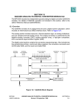
System Integration Module Block Diagram .................................................... 5-2
System Clock Block Diagram ......................................................................... 5-4
System Clock Oscillator Circuit ...................................................................... 5-5
System Clock Filter Networks ........................................................................ 5-6
LPSTOP Flowchart ....................................................................................... 5-13
System Protection Block .............................................................................. 5-14
Periodic Interrupt Timer and Software Watchdog Timer .............................. 5-17
MCU Basic System ...................................................................................... 5-20
Operand Byte Order ..................................................................................... 5-25
Word Read Cycle Flowchart ......................................................................... 5-28
Write Cycle Flowchart .................................................................................. 5-29
CPU Space Address Encoding .................................................................... 5-31
Breakpoint Operation Flowchart ................................................................... 5-33
LPSTOP Interrupt Mask Level ...................................................................... 5-34
Bus Arbitration Flowchart for Single Request ............................................... 5-39
Preferred Circuit for Data Bus Mode Select Conditioning ............................ 5-43
Alternate Circuit for Data Bus Mode Select Conditioning ............................. 5-44
Power-On Reset ........................................................................................... 5-49
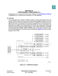
Basic MCU System ...................................................................................... 5-55
Chip-Select Circuit Block Diagram ............................................................... 5-56
CPU Space Encoding for Interrupt Acknowledge ......................................... 5-61
MC68336/376
USER’S MANUAL
MOTOROLA
xvii
336376UMBook Page xviii Friday, November 15, 1996 2:09 PM
LIST OF ILLUSTRATIONS
(Continued)
Title
Figure
8-1
8-2
8-3
8-4
8-5
8-6
8-7
8-8
8-9
8-10
8-11
9-1
9-2
9-3
9-4
9-5
9-6
9-7
9-8
9-9
9-10
9-11
10-1
10-2
10-3
10-4
10-5
10-6
11-1
11-2
11-3
13-1
13-2
13-3
13-4
13-5
A-1
A-2
A-3
A-4
A-5
Page
QADC Block Diagram ..................................................................................... 8-1
QADC Input and Output Signals .................................................................... 8-3
Example of External Multiplexing ................................................................. 8-11
QADC Module Block Diagram ...................................................................... 8-13
Conversion Timing ....................................................................................... 8-14
Bypass Mode Conversion Timing ................................................................. 8-15
QADC Queue Operation with Pause ............................................................ 8-18
QADC Clock Subsystem Functions .............................................................. 8-24
QADC Clock Programmability Examples ..................................................... 8-26
QADC Conversion Queue Operation ........................................................... 8-29
QADC Interrupt Vector Format ..................................................................... 8-33
QSM Block Diagram ....................................................................................... 9-1
QSPI Block Diagram ...................................................................................... 9-5
QSPI RAM ...................................................................................................... 9-7
Flowchart of QSPI Initialization Operation .................................................... 9-10
Flowchart of QSPI Master Operation (Part 1) .............................................. 9-11
Flowchart of QSPI Master Operation (Part 2) .............................................. 9-12
Flowchart of QSPI Master Operation (Part 3) .............................................. 9-13
Flowchart of QSPI Slave Operation (Part 1) ................................................ 9-14
Flowchart of QSPI Slave Operation (Part 2) ................................................ 9-15
SCI Transmitter Block Diagram .................................................................... 9-22
SCI Receiver Block Diagram ........................................................................ 9-23
CTM4 Block Diagram ................................................................................... 10-1
CPSM Block Diagram ................................................................................... 10-4
FCSM Block Diagram ................................................................................... 10-5
MCSM Block Diagram .................................................................................. 10-8
DASM Block Diagram ................................................................................. 10-11
Pulse-Width Modulation Submodule Block Diagram .................................. 10-13
TPU Block Diagram ...................................................................................... 11-1
TCR1 Prescaler Control ............................................................................. 11-14
TCR2 Prescaler Control ............................................................................. 11-14
TouCAN Block Diagram ............................................................................... 13-1
Typical CAN Network ................................................................................... 13-2
Extended ID Message Buffer Structure ........................................................ 13-3
Standard ID Message Buffer Structure ........................................................ 13-4
TouCAN Interrupt Vector Generation ......................................................... 13-19
CLKOUT Output Timing Diagram ................................................................. A-10
External Clock Input Timing Diagram ........................................................... A-10
ECLK Output Timing Diagram ...................................................................... A-10
Read Cycle Timing Diagram ........................................................................ A-11
Write Cycle Timing Diagram ......................................................................... A-12
MOTOROLA
xviii
MC68336/376
USER’S MANUAL
336376UMBook Page xix Friday, November 15, 1996 2:09 PM
LIST OF ILLUSTRATIONS
(Continued)
Title
Figure
A-6
A-7
A-8
A-9
A-10
A-11
A-12
A-13
A-14
A-15
A-16
A-17
A-18
A-19
A-20
B-1
B-2
B-3
D-1
D-2
D-3
Page
Fast Termination Read Cycle Timing Diagram ............................................ A-13
Fast Termination Write Cycle Timing Diagram ............................................. A-14
Bus Arbitration Timing Diagram — Active Bus Case ................................... A-15
Bus Arbitration Timing Diagram — Idle Bus Case ....................................... A-16
Show Cycle Timing Diagram ........................................................................ A-17
Chip-Select Timing Diagram ........................................................................ A-18
Reset and Mode Select Timing Diagram ...................................................... A-18
Background Debugging Mode Timing — Serial Communication ................. A-20
Background Debugging Mode Timing — Freeze Assertion ......................... A-20
ECLK Timing Diagram .................................................................................. A-22
QSPI Timing — Master, CPHA = 0 .............................................................. A-24
QSPI Timing — Master, CPHA = 1 .............................................................. A-24
QSPI Timing — Slave, CPHA = 0 ................................................................ A-25
QSPI Timing — Slave, CPHA = 1 ................................................................ A-25
TPU Timing Diagram .................................................................................... A-26
MC68336 Pin Assignments for 160-Pin Package .......................................... B-1
MC68376 Pin Assignments for 160-Pin Package .......................................... B-2
160-Pin Package Dimensions ........................................................................ B-3
User Programming Model ..............................................................................D-2
Supervisor Programming Model Supplement .................................................D-3
TouCAN Message Buffer Address Map .......................................................D-85
MC68336/376
USER’S MANUAL
MOTOROLA
xix
336376UMBook Page xx Friday, November 15, 1996 2:09 PM
LIST OF ILLUSTRATIONS
Figure
MOTOROLA
xx
(Continued)
Title
Page
MC68336/376
USER’S MANUAL
336376UMBook Page xxi Friday, November 15, 1996 2:09 PM
LIST OF TABLES
Table
3-1
3-2
3-3
3-4
3-5
4-1
4-2
4-3
4-4
4-5
4-6
4-7
5-1
5-2
5-3
5-4
5-5
5-6
5-7
5-8
5-9
5-10
5-11
5-12
5-13
5-14
5-15
5-16
5-17
5-18
5-19
5-20
5-21
5-22
6-1
7-1
7-2
8-1
8-2
8-3
8-4
Title
Page
MC68336/376 Pin Characteristics................................................................... 3-7
MC68336/376 Output Driver Types................................................................. 3-8
MC68336/376 Power Connections.................................................................. 3-8
MC68336/376 Signal Characteristics .............................................................. 3-9
MC68336/376 Signal Functions .................................................................... 3-11
Unimplemented MC68020 Instructions ......................................................... 4-10
Instruction Set Summary ............................................................................... 4-11
Exception Vector Assignments...................................................................... 4-16
BDM Source Summary.................................................................................. 4-20
Polling the BDM Entry Source....................................................................... 4-21
Background Mode Command Summary ....................................................... 4-22
CPU Generated Message Encoding ............................................................. 4-25
Show Cycle Enable Bits .................................................................................. 5-3
Clock Control Multipliers.................................................................................. 5-8
System Frequencies from 4.194 MHz Reference ......................................... 5-10
Bus Monitor Period........................................................................................ 5-15
MODCLK Pin and SWP Bit During Reset ..................................................... 5-16
Software Watchdog Ratio.............................................................................. 5-16
MODCLK Pin and PTP Bit at Reset .............................................................. 5-17
Periodic Interrupt Priority............................................................................... 5-18
Size Signal Encoding .................................................................................... 5-22
Address Space Encoding ............................................................................. 5-23
Effect of DSACK Signals ............................................................................... 5-24
Operand Alignment ....................................................................................... 5-26
DSACK, BERR, and HALT Assertion Results............................................... 5-35
Reset Source Summary ................................................................................ 5-41
Reset Mode Selection ................................................................................... 5-42
Module Pin Functions During Reset.............................................................. 5-46
SIM Pin Reset States .................................................................................... 5-47
Chip-Select Pin Functions ............................................................................. 5-57
Pin Assignment Field Encoding..................................................................... 5-58
Block Size Encoding...................................................................................... 5-59
Chip-Select Base and Option Register Reset Values ................................... 5-63
CSBOOT Base and Option Register Reset Values....................................... 5-63
SRAM Array Address Space Type .................................................................. 6-2
ROM Array Space Type .................................................................................. 7-2
Wait States Field ............................................................................................. 7-2
Multiplexed Analog Input Channels................................................................. 8-5
Analog Input Channels .................................................................................. 8-12
Queue 1 Priority Assertion ............................................................................ 8-17
QADC Clock Programmability ....................................................................... 8-27
MC68336/376
USER’S MANUAL
MOTOROLA
xxi
336376UMBook Page xxii Friday, November 15, 1996 2:09 PM
LIST OF TABLES
(Continued)
Title
Table
8-5
9-1
9-2
9-3
9-4
9-5
9-6
10-1
10-2
10-3
10-4
10-5
10-6
10-7
11-1
11-2
11-3
11-4
13-1
13-2
13-3
13-4
13-5
13-6
13-7
13-8
13-9
A-1
A-2
A-3
A-4
A-5
A-6
A-7
A-8
A-9
A-10
A-11
A-12
A-13
A-14
Page
QADC Status Flags and Interrupt Sources ................................................... 8-32
Effect of DDRQS on QSM Pin Function .......................................................... 9-4
QSPI Pins........................................................................................................ 9-8
Bits Per Transfer ........................................................................................... 9-17
SCI Pins ........................................................................................................ 9-24
Serial Frame Formats.................................................................................... 9-25
Effect of Parity Checking on Data Size ......................................................... 9-26
CTM4 Time Base Bus Allocation................................................................... 10-3
DASM Modes of Operation ......................................................................... 10-10
Channel B Data Register Access ................................................................ 10-11
PWMSM Divide By Options......................................................................... 10-14
PWM Pulse and Frequency Ranges (in Hz) Using ÷ 2 Option (20.97 MHz)10-16
PWM Pulse and Frequency Ranges (in Hz) Using ÷ 3 Option (20.97 MHz)10-16
CTM4 Interrupt Priority and Vector/Pin Allocation....................................... 10-18
TCR1 Prescaler Control .............................................................................. 11-14
TCR2 Prescaler Control .............................................................................. 11-15
TPU Function Encodings............................................................................. 11-16
Channel Priority Encodings ......................................................................... 11-17
Common Extended/Standard Format Frames .............................................. 13-4
Message Buffer Codes for Receive Buffers .................................................. 13-4
Message Buffer Codes for Transmit Buffers ................................................. 13-5
Extended Format Frames.............................................................................. 13-5
Standard Format Frames .............................................................................. 13-6
Receive Mask Register Bit Values ................................................................ 13-7
Mask Examples for Normal/Extended Messages.......................................... 13-8
Example System Clock, CAN Bit Rate and S-Clock Frequencies................. 13-9
Interrupt Sources and Vector Addresses .................................................... 13-20
Maximum Ratings........................................................................................... A-1
Typical Ratings............................................................................................... A-2
Thermal Characteristics ................................................................................. A-2
Clock Control Timing ...................................................................................... A-3
DC Characteristics ......................................................................................... A-4
AC Timing...................................................................................................... A-7
Background Debug Mode Timing................................................................. A-19
ECLK Bus Timing ......................................................................................... A-21
QSPI Timing ................................................................................................. A-23
Time Processor Unit Timing ......................................................................... A-26
QADC Maximum Ratings ............................................................................. A-27
QADC DC Electrical Characteristics (Operating) ......................................... A-28
QADC AC Electrical Characteristics (Operating) ......................................... A-29
QADC Conversion Characteristics (Operating)............................................ A-30
MOTOROLA
xxii
MC68336/376
USER’S MANUAL
336376UMBook Page xxiii Friday, November 15, 1996 2:09 PM
LIST OF TABLES
(Continued)
Title
Table
A-15
A-16
A-17
A-18
A-19
B-1
B-2
D-1
D-2
D-3
D-4
D-5
D-6
D-7
D-8
D-9
D-10
D-11
D-12
D-13
D-14
D-15
D-16
D-17
D-18
D-19
D-20
D-21
D-22
D-23
D-24
D-25
D-26
D-27
D-28
D-29
D-30
D-31
D-32
D-33
D-34
Page
FCSM Timing Characteristics....................................................................... A-31
MCSM Timing Characteristics...................................................................... A-31
SASM Timing Characteristics....................................................................... A-32
DASM Timing Characteristics ...................................................................... A-33
PWMSM Timing Characteristics................................................................... A-34
MC68336 Ordering Information...................................................................... B-4
MC68376 Ordering Information...................................................................... B-5
Module Address Map .....................................................................................D-1
T[1:0] Encoding ..............................................................................................D-3
SIM Address Map...........................................................................................D-5
Show Cycle Enable Bits .................................................................................D-7
Port E Pin Assignments................................................................................D-11
Port F Pin Assignments................................................................................D-12
Software Watchdog Timing Field .................................................................D-13
Bus Monitor Time-Out Period.......................................................................D-13
Pin Assignment Field Encoding....................................................................D-15
CSPAR0 Pin Assignments ...........................................................................D-16
CSPAR1 Pin Assignments ...........................................................................D-16
Reset Pin Function of CS[10:6] ....................................................................D-17
Block Size Field Bit Encoding.......................................................................D-18
BYTE Field Bit Encoding ..............................................................................D-19
Read/Write Field Bit Encoding .....................................................................D-19
DSACK Field Encoding ................................................................................D-20
Address Space Bit Encodings ......................................................................D-20
Interrupt Priority Level Field Encoding .........................................................D-20
SRAM Address Map.....................................................................................D-22
RASP Encoding............................................................................................D-22
MRM Address Map.......................................................................................D-24
ROM Array Space Field ...............................................................................D-25
Wait States Field ..........................................................................................D-25
QADC Address Map.....................................................................................D-28
Queue 1 Operating Modes ...........................................................................D-32
Queue 2 Operating Modes ...........................................................................D-34
Queue Status ...............................................................................................D-36
Input Sample Times .....................................................................................D-37
Non-multiplexed Channel Assignments and Pin Designations ....................D-38
Multiplexed Channel Assignments and Pin Designations ............................D-38
QSM Address Map .......................................................................................D-40
PQSPAR Pin Assignments...........................................................................D-47
Effect of DDRQS on QSM Pin Function .......................................................D-48
Bits Per Transfer ..........................................................................................D-49
MC68336/376
USER’S MANUAL
MOTOROLA
xxiii
336376UMBook Page xxiv Friday, November 15, 1996 2:09 PM
LIST OF TABLES
(Continued)
Title
Table
D-35
D-36
D-37
D-38
D-39
D-40
D-41
D-42
D-43
D-44
D-45
D-46
D-47
D-48
D-49
D-50
D-51
D-52
D-53
D-54
D-55
D-56
D-57
D-58
D-59
D-60
D-61
D-62
D-63
Page
CTM4 Address Map .....................................................................................D-56
Interrupt Vector Base Number Bit Field........................................................D-57
Time Base Register Bus Select Bits.............................................................D-58
Prescaler Division Ratio Select Field ...........................................................D-59
Drive Time Base Bus Field...........................................................................D-60
Counter Clock Select Field...........................................................................D-60
Drive Time Base Bus Field...........................................................................D-62
Modulus Load Edge Sensitivity Bits .............................................................D-62
Counter Clock Select Field...........................................................................D-62
DASM Mode Flag Status Bit States .............................................................D-64
Edge Polarity ................................................................................................D-65
DASM Mode Select Field .............................................................................D-66
DASMA Operations ......................................................................................D-67
DASMB Operations ......................................................................................D-68
PWMSM Output Pin Polarity Selection ........................................................D-70
PWMSM Divide By Options..........................................................................D-71
TPU Register Map........................................................................................D-73
TCR1 Prescaler Control Bits ........................................................................D-74
TCR2 Prescaler Control Bits ........................................................................D-74
FRZ[1:0] Encoding .......................................................................................D-76
Breakpoint Enable Bits .................................................................................D-76
Channel Priorities .........................................................................................D-80
Parameter RAM Address Map .....................................................................D-81
TPURAM Address Map ................................................................................D-82
TouCAN Address Map .................................................................................D-84
RX MODE[1:0] Configuration .......................................................................D-89
Transmit Pin Configuration...........................................................................D-89
Transmit Bit Error Status ..............................................................................D-94
Fault Confinement State Encoding...............................................................D-95
MOTOROLA
xxiv
MC68336/376
USER’S MANUAL
336376UMBook Page 1 Friday, November 15, 1996 2:09 PM
SECTION 1 INTRODUCTION
The MC68336 and the MC68376 are highly-integrated 32-bit microcontrollers, combining high-performance data manipulation capabilities with powerful peripheral
subsystems.
MC68300 microcontrollers are built up from standard modules that interface through
a common intermodule bus (IMB). Standardization facilitates rapid development of
devices tailored for specific applications.
The MC68336 incorporates a 32-bit CPU (CPU32), a system integration module
(SIM), a time processor unit (TPU), a configurable timer module (CTM4), a queued
serial module (QSM), a 10-bit queued analog-to-digital converter module (QADC), a
3.5-Kbyte TPU emulation RAM module (TPURAM), and a 4-Kbyte standby RAM
module (SRAM).
The MC68376 includes all of the aforementioned modules, plus a CAN 2.0B protocol
controller module (TouCAN™) and an 8-Kbyte masked ROM (MRM).
The MC68336/376 can either synthesize the system clock signal from a fast reference
or use an external clock input directly. Operation with a 4.194 MHz reference frequency is standard. The maximum system clock speed is 20.97 MHz. System hardware
and software allow changes in clock rate during operation. Because MCU operation is
fully static, register and memory contents are not affected by clock rate changes.
High-density complementary metal-oxide semiconductor (HCMOS) architecture
makes the basic power consumption of the MCU low. Power consumption can be minimized by stopping the system clock. The CPU32 instruction set includes a low-power
stop (LPSTOP) instruction that efficiently implements this capability.
Documentation for the Modular Microcontroller Family follows the modular construction of the devices in the product line. Each microcontroller has a comprehensive
user's manual that provides sufficient information for normal operation of the device.
The user's manual is supplemented by module reference manuals that provide detailed information about module operation and applications. Refer to Motorola publication Advanced Microcontroller Unit (AMCU) Literature (BR1116/D) for a complete
listing of documentation.
MC68336/376
USER’S MANUAL
INTRODUCTION
MOTOROLA
1-1
336376UMBook Page 2 Friday, November 15, 1996 2:09 PM
MOTOROLA
1-2
INTRODUCTION
MC68336/376
USER’S MANUAL
336376UMBook Page 1 Friday, November 15, 1996 2:09 PM
SECTION 2 NOMENCLATURE
The following nomenclature is used throughout the manual. Nomenclature used only
in certain sections, such as register bit mnemonics, is defined in those sections.
2.1 Symbols and Operators
+ — Addition
− — Subtraction or negation (two's complement)
∗ — Multiplication
/ — Division
> — Greater
< — Less
= — Equal
≥ — Equal or greater
≤ — Equal or less
≠ — Not equal
• — AND
✛ — Inclusive OR (OR)
⊕ — Exclusive OR (EOR)
NOT — Complementation
: — Concatenation
⇒ — Transferred
⇔ — Exchanged
± — Sign bit; also used to show tolerance
« — Sign extension
% — Binary value
$ — Hexadecimal value
MC68336/376
USER’S MANUAL
NOMENCLATURE
MOTOROLA
2-1
336376UMBook Page 2 Friday, November 15, 1996 2:09 PM
2.2 CPU32 Registers
A6–A0 — Address registers (index registers)
A7 (SSP) — Supervisor stack pointer
A7 (USP) — User stack pointer
CCR
D7–D0
DFC
PC
SFC
SR
—
—
—
—
—
—
Condition code register (user portion of SR)
Data registers (index registers)
Alternate function code register
Program counter
Alternate function code register
Status register
VBR — Vector base register
X — Extend indicator
N — Negative indicator
Z — Zero indicator
V — Two’s complement overflow indicator
C — Carry/borrow indicator
2.3 Pin and Signal Mnemonics
ADDR[23:0]
AN[59:48]/[3:0]
AN[w, x, y, z]
AS
AVEC
BERR
BG
BGACK
BKPT
BR
CANRX0
CANTX0
CLKOUT
CS[10:0]
CSBOOT
CPWM[8:5]
CTD[10:9]/[4:3]
CTM2C
DATA[15:0]
DS
MOTOROLA
2-2
—
—
—
—
—
—
—
—
—
—
—
—
—
—
—
—
—
—
—
—
Address Bus
QADC Analog Input
QADC Analog Input
Address Strobe
Autovector
Bus Error
Bus Grant
Bus Grant Acknowledge
Breakpoint
Bus Request
TouCAN Receive Data
TouCAN Transmit Data
System Clock
Chip Selects
Boot ROM Chip Select
CTM Pulse Width Modulation Channel
CTM Double Action Channel
CTM Modulus Clock
Data Bus
Data Strobe
NOMENCLATURE
MC68336/376
USER’S MANUAL
336376UMBook Page 3 Friday, November 15, 1996 2:09 PM
DSACK[1:0]
DSCLK
DSI
DSO
ECLK
ETRIG[2:1]
EXTAL
FC[2:0]
FREEZE
HALT
IFETCH
IPIPE
IRQ[7:1]
MA[2:0]
MISO
MODCLK
MOSI
PCS[3:0]
PQA[7:0]
PQB[7:0]
PC[6:0]
PE[7:0]
PF[7:0]
QUOT
R/W
RESET
RMC
RXD
SCK
SIZ[1:0]
SS
T2CLK
TPUCH[15:0]
TSC
TSTME
VRH
—
—
—
—
—
—
—
—
—
—
—
—
—
—
—
—
—
—
—
—
—
—
—
—
—
—
—
—
—
—
—
—
—
—
—
Data and Size Acknowledge
Development Serial Clock
Development Serial Input
Development Serial Output
MC6800 Devices and Peripherals Bus Clock
QADC External Trigger
Crystal Oscillator Input
Function Codes
Freeze
Halt
Instruction Fetch
Instruction Pipeline
Interrupt Request
QADC Multiplexed Address
QSM Master In Slave Out
Clock Mode Select
QSM Master Out Slave In
QSM Peripheral Chip-Selects
QADC Port A
QADC Port B
SIM Port C
SIM Port E
SIM Port F
Quotient Out
Read/Write
Reset
Read-Modify-Write Cycle
SCI Receive Data
QSPI Serial Clock
Size
Slave Select
TPU Clock In
TPU Channel Signals
Three-State Control
Test Mode Enable
— QADC High Reference Voltage
VRL — QADC Low Reference Voltage
XFC — External Filter Capacitor
XTAL — Crystal Oscillator Output
MC68336/376
USER’S MANUAL
NOMENCLATURE
MOTOROLA
2-3
336376UMBook Page 4 Friday, November 15, 1996 2:09 PM
2.4 Register Mnemonics
BIUMCR — CTM4 BIUSM Module Configuration
BIUTEST — CTM4 BIUSM Test Register
BIUTBR — CTM4 BIUSM Time Base Register
CANCTRL[0:2]
CANICR
IFLAG
IMASK
CANMCR
CANTCR
—
—
—
—
—
TouCAN Control Register [0:2]
TouCAN Interrupt Configuration Register
TouCAN Interrupt Flags Register
TouCAN Interrupt Masks Register
TouCAN Module Configuration Register
TouCAN Test Configuration Register
CCW[0:27] — QADC Command Conversion Words [0:27]
CFSR[0:3] — TPU Channel Function Select Registers [0:3]
CIER — TPU Channel Interrupt Enable Register
CISR — TPU Channel Interrupt Status Register
CPCR — CTM4 CPSM Control Register
CPR[0:1] — TPU Channel Priority Registers [0:1]
CPTR
CR[0:F]
CREG
CSBARBT
CSBAR[0:10]
—
—
—
—
—
CTM4 CPSM Test Register
QSM Command RAM
SIM Test Control Register C
SIM Chip-Select Base Address Register Boot ROM
SIM Chip-Select Base Address Registers [0:10]
CSORBT
CSOR[0:10]
CSPAR[0:1]
DASM[3:4]/[9:10]A
DASM[3:4]/[9:10]B
—
—
—
—
—
SIM Chip-Select Option Register Boot ROM
SIM Chip-Select Option Registers [0:10]
SIM Chip-Select Pin Assignment Registers [0:1]
CTM4 DASM A Registers [3:4]/[9:10]
CTM4 DASM B Registers [3:4]/[9:10]
DASM[3:4]/[9:10]SIC
DCNR
DDRE
DDRF
DDRQA
DDRQS
DREG
DSCR
DSSR
ESTAT
—
—
—
—
—
—
—
—
—
—
CTM4 DASM Status/Interrupt/Control Registers [3:4]/[9:10]
Decoded Channel Number Register
SIM Port E Data Direction Register
SIM Port F Data Direction Register
QADC Port A Data Direction Register
QSM Port QS Data Direction Register
SIM Test Module Distributed Register
TPU Development Support Control Register
TPU Development Support Status Register
TouCAN Error and Status Register
MOTOROLA
2-4
NOMENCLATURE
MC68336/376
USER’S MANUAL
336376UMBook Page 5 Friday, November 15, 1996 2:09 PM
FCSM12CNT — CTM4 FCSM12 Counter Register
FCSM12SIC — CTM4 FCSM12 Status/Interrupt/Control Register
HSQR[0:1] — TPU Host Sequence Registers [0:1]
HSRR[0:1] — TPU Host Service Request Registers [0:1]
LJSRR[0:27] — QADC Left-Justified Signed Result Registers [0:27]
LJURR[0:27] — QADC Left-Justified Unsigned Result Registers [0:27]
LR
MCSM[2]/[11]CNT
MCSM[2]/[11]ML
MCSM[2]/[11]SIC
MRMCR
PEPAR
PFPAR
—
—
—
—
—
—
—
Link Register
CTM4 MCSM Counter Registers [2]/[11]
CTM4 MCSM Modulus Latch Registers [2]/[11]
CTM4 MCSM Status/Interrupt/Control Registers [2]/[11]
Masked ROM Module Configuration Register
SIM Port E Pin Assignment Register
SIM Port F Pin Assignment Register
PICR
PITR
PORTC
PORTE
PORTF
—
—
—
—
—
SIM Periodic Interrupt Control Register
SIM Periodic Interrupt Timer Register
SIM Port C Data Register
SIM Port E Data Register
SIM Port F Data Register
PORTQA
PORTQB
PORTQS
PQSPAR
PRESDIV
—
—
—
—
—
QADC Port A Data Register
QADC Port B Data Register
QSM Port QS Data Register
QSM Port QS Pin Assignment Register
TouCAN Prescaler Divide Register
PWM[5:8]C
PWM[5:8]A
PWM[5:8]B
PWM[5:8]SIC
QACR[0:1]
QADCINT
QADCMCR
QADCTEST
QASR
QILR
QIVR
QSMCR
QTEST
—
—
—
—
—
—
—
—
—
—
—
—
—
CTM4 PWMSM Counter Registers [5:8]
CTM4 PWMSM Period Registers [5:8]
CTM4 PWMSM Pulse Width Registers [5:8]
CTM4 PWMSM Status/Interrupt/Control Registers [5:8]
QADC Control Registers [0:2]
QADC Interrupt Register
QADC Module Configuration Register
QADC Test Register
QADC Status Register
QSM Interrupt Level Register
QSM Interrupt Vector Register
QSM Module Configuration Register
QSM Test Register
RAMBAH — RAM Base Address High Register
MC68336/376
USER’S MANUAL
NOMENCLATURE
MOTOROLA
2-5
336376UMBook Page 6 Friday, November 15, 1996 2:09 PM
RAMBAL — RAM Base Address Low Register
RAMMCR — RAM Module Configuration Register
RAMTST — RAM Test Register
ROMBAH — ROM Base Address High Register
ROMBAL — ROM Base Address Low Register
RR[0:F] — QSM Receive RAM
RSIGHI
RSIGLO
ROMBS[0:3]
RXGMSKHI
RXGMSKLO
RX[14:15]MSKHI
RX[14:15]MSKLO
—
—
—
—
—
—
—
ROM Signature High Register
ROM Signature Low Register
ROM Bootstrap Words [0:3]
TouCAN Receive Global Mask High Register
TouCAN Receive Global Mask Low Register
TouCAN Receive Buffer [14:15] Mask High Registers
TouCAN Receive Buffer [14:15] Mask Low Registers
RJURR[0:27]
RSR
RXECTR
SCCR[0:1]
SCDR
—
—
—
—
—
QADC Right-Justified Unsigned Result Registers
SIM Reset Status Register
TouCAN Receive Error Counter Register
QSM SCI Control Registers [0:1]
QSM SCI Data Register
SCSR
SGLR
SIMCR
SIMTR
SIMTRE
—
—
—
—
—
QSM SCI Status Register
Service Grant Latch Register
SIM Module Configuration Register
SIM System Integration Test Register
SIM System Integration Test Register (ECLK)
SPCR[0:3]
SPSR
SWSR
SYNCR
SYPCR
TICR
TIMER
TPUMCR
TR[0:F]
TRAMBAR
TRAMMCR
TRAMTST
TSTMSRA
—
—
—
—
—
—
—
—
—
—
—
—
—
QSM QSPI Control Registers [0:3]
QSM QSPI Status Register
SIM Software Watchdog Service Register
SIM Clock Synthesizer Control Register
SIM System Protection Control Register
TPU Interrupt Configuration Register
TouCAN Free Running Timer Register
TPU Module Configuration Register
QSM Transmit RAM
TPURAM Base Address Register
TPURAM Module Configuration Register
TPURAM Test Register
SIM Test Module Master Shift Register A
TSTMSRB — SIM Test Module Master Shift Register B
MOTOROLA
2-6
NOMENCLATURE
MC68336/376
USER’S MANUAL
336376UMBook Page 7 Friday, November 15, 1996 2:09 PM
TSTRC — SIM Test Module Repetition Counter Register
TSTSC — SIM Test Module Shift Count Register
TTR — TouCAN Test Register
TXECTR — TouCAN Transmit Error Counter Register
MC68336/376
USER’S MANUAL
NOMENCLATURE
MOTOROLA
2-7
336376UMBook Page 8 Friday, November 15, 1996 2:09 PM
2.5 Conventions
Logic level one is the voltage that corresponds to a Boolean true (1) state.
Logic level zero is the voltage that corresponds to a Boolean false (0) state.
Set refers specifically to establishing logic level one on a bit or bits.
Clear refers specifically to establishing logic level zero on a bit or bits.
Asserted means that a signal is in active logic state. An active low signal changes
from logic level one to logic level zero when asserted. An active high signal changes
from logic level zero to logic level one.
Negated means that an asserted signal changes logic state. An active low signal
changes from logic level zero to logic level one when negated. An active high signal
changes from logic level one to logic level zero.
A specific mnemonic within a range is referred to by mnemonic and number. A15 is
bit 15 of accumulator A; ADDR7 is line 7 of the address bus; CSOR0 is chip-select option register 0. A range of mnemonics is referred to by mnemonic and the numbers
that define the range. VBR[4:0] are bits four to zero of the vector base register;
CSOR[0:5] are the first six option registers.
Parentheses are used to indicate the content of a register or memory location rather
than the register or memory location itself. (A) is the content of accumulator A. (M : M
+ 1) is the content of the word at address M.
LSB means least significant bit. MSB means most significant bit. References to low
and high bytes are spelled out.
LSW means least significant word. MSW means most significant word.
ADDR is the address bus. ADDR[7:0] are the eight LSBs of the address bus.
DATA is the data bus. DATA[15:8] are the eight MSBs of the data bus.
MOTOROLA
2-8
NOMENCLATURE
MC68336/376
USER’S MANUAL
336376UMSect3Overview Page 1 Thursday, December 5, 1996 4:45 PM
SECTION 3 OVERVIEW
This section contains information about the entire MC68336/376 modular microcontroller. It lists the features of each module, shows device functional divisions and pin
assignments, summarizes signal and pin functions, discusses the intermodule bus,
and provides system memory maps. Timing and electrical specifications for the entire
microcontroller and for individual modules are provided in APPENDIX A ELECTRICAL CHARACTERISTICS. Comprehensive module register descriptions and memory maps are provided in APPENDIX D REGISTER SUMMARY.
3.1 MCU Features
The following paragraphs highlight capabilities of each of the microcontroller modules.
Each module is discussed separately in a subsequent section of this user's manual.
3.1.1 Central Processing Unit (CPU32)
• 32-bit architecture
• Virtual memory implementation
• Table look-up and interpolate instruction
• Improved exception handling for controller applications
• High level language support
• Background debug mode
• Fully static operation
3.1.2 System Integration Module (SIM)
• External bus support
• Programmable chip select outputs
• System protection logic
• Watchdog timer, clock monitor and bus monitor
• Two 8-bit dual function input/output ports
• One 7-bit dual function output port
• Phase-locked loop (PLL) clock system
3.1.3 Standby RAM Module (SRAM)
• 4-Kbytes of static RAM
• No standby supply
3.1.4 Masked ROM Module (MRM)
• 8-Kbyte array, accessible as bytes or words
• User selectable default base address
• User selectable bootstrap ROM function
• User selectable ROM verification code
MC68336/376
USER’S MANUAL
OVERVIEW
MOTOROLA
3-1
336376UMSect3Overview Page 2 Thursday, December 5, 1996 4:45 PM
3.1.5 10-Bit Queued Analog-to-Digital Converter (QADC)
• 16 channels internally; up to 44 directly accessible channels with external multiplexing
• Six automatic channel selection and conversion modes
• Two channel scan queues of variable length, each with a variable number of subqueues
• 40 result registers and three result alignment formats
• Programmable input sample time
• Direct control of external multiplexers
3.1.6 Queued Serial Module (QSM)
• Enhanced serial communications interface (SCI)
• Modulus baud rate generator
• Parity detection
• Queued serial peripheral interface (QSPI)
• 80-byte static RAM to perform queued operations
• Up to 16 automatic transfers
• Continuous cycling, 8 to 16 bits per transfer, LSB or MSB first
• Dual function I/O pins
3.1.7 Configurable Timer Module Version 4 (CTM4)
• Two 16-bit modulus counter submodules (MCSMs)
• 16-bit free-running counter submodule (FCSM)
• Four double-action submodules (DASMs)
• Four pulse-width submodules (PWMSMs)
3.1.8 Time Processor Unit (TPU)
• Dedicated micro-engine operating independently of the CPU32
• 16 independent programmable channels and pins
• Each channel has an event register consisting of a 16-bit capture register, a 16bit compare register and a 16-bit comparator
• Any channel can perform any time function
• Each channel has six or eight 16-bit parameter registers
• Each timer function may be assigned to more than one channel
• Two timer counter registers with programmable prescalers
• Each channel can be synchronized to one or both counters
• Selectable channel priority levels
3.1.9 Static RAM Module with TPU Emulation Capability (TPURAM)
• 3.5 Kbytes of static RAM
• External VSTBY pin for separate standby supply
• May be used as normal RAM or TPU microcode emulation RAM
MOTOROLA
3-2
OVERVIEW
MC68336/376
USER’S MANUAL
336376UMSect3Overview Page 3 Thursday, December 5, 1996 4:45 PM
3.1.10 CAN 2.0B Controller Module (TouCAN)
• Full implementation of CAN protocol specification, version 2.0 A and B
• 16 receive/transmit message buffers of 0 to 8 bytes data length
• Global mask register for message buffers 0 to 13
• Independent mask registers for message buffers 14 and 15
• Programmable transmit-first scheme: lowest ID or lowest buffer number
• 16-bit free-running timer for message time-stamping
• Low power sleep mode with programmable wake-up on bus activity
3.2 Intermodule Bus
The intermodule bus (IMB) is a standardized bus developed to facilitate both design
and operation of modular microcontrollers. It contains circuitry to support exception
processing, address space partitioning, multiple interrupt levels, and vectored interrupts. The standardized modules in the MCU communicate with one another through
the IMB. The IMB in the MCU uses 24 address and 16 data lines.
3.3 System Block Diagram and Pin Assignment Diagrams
Figure 3-1 is a functional diagram of the MCU. There is not a one-to-one correspondence between location and size of blocks in the diagram and location and size of integrated-circuit modules. Figure 3-2 shows the MC68336 pin assignment package;
Figure 3-3 shows the MC68376 pin assignment package. Note that the MC68376 is
a pin-compatible upgrade for the MC68336 that provides a CAN protocol controller
and an 8-Kbyte masked ROM module. Both devices use a 160-pin plastic surfacemount package. Refer to B.1 Obtaining Updated MC68336/376 Mechanical Information for package dimensions. Refer to subsequent paragraphs in this section for
pin and signal descriptions.
MC68336/376
USER’S MANUAL
OVERVIEW
MOTOROLA
3-3
T2CLK
VSTBY
CTM2C
CTD[10:9]/CTD[4:3]
CPWM[8:5]
CANTX0
CANRX0
TPUCH[15:0]
336376UMSect3Overview Page 4 Thursday, December 5, 1996 4:45 PM
CSBOOT
VDD
VSS
BR/CS0
BG/CS1
BGACK/CS2
3.5
KBYTE
TPURAM
TPU
CHIP
SELECTS
BGACK
BR
BG
FC0
ADDR23/CS10/ECLK
ADDR22/CS9/PC6
PORT C
CTM4
CONTROL
CS[10:0]
8K
MRM
MC68376
ONLY
TouCAN
MC68376 ONLY
FC2/CS5/PC2
FC2
FC1/CS4/PC1
FC0/CS3/PC0
ADDR[18:0]
DSACK0
SIZ1/PE7
DSACK1
SIZ0/PE6
AVEC
AS
PORT E
DS
AS/PE5
CONTROL
RMC
EBI
ADDR20/CS7/PC4
ADDR19/CS6/PC3
FC1
ADDR
[23:19]
1
FCSM
2
MCSMs
4
DASMs
4
PWMSMs
ADDR21/CS8/PC5
DS/PE4
RMC/PE3
AVEC/PE2
SIZ0
DSACK1/PE1
SIZ1
DSACK0/PE0
DATA[15:0]
IMB
R/W
RESET
HALT
4K
SRAM
QADC
QSM
BERR
MODCLK/PF0
CPU32
IRQ[7:1]
RXD
PCS0/SS/PQS3
SCK/PQS2
PORT QS
PCS2/PQS5
PORT F
MODCLK
CONTROL
TXD/PQS7
PCS3/PQS6
PCS1/PQS4
IRQ7/PF7
IRQ6/PF6
IRQ5/PF5
IRQ4/PF4
IRQ3/PF3
IRQ2/PF2
CLOCK
IRQ1/PF1
CLKOUT
MOSI/PQS1
XTAL
MISO/PQS0
EXTAL
TEST
TSC
TSTME
QUOT
FREEZE
TSTME/TSC
CONTROL
PORT QA
PORT QB
XFC
VDDSYN
FREEZE/QUOT
IFETCH
IPIPE
DSI
DSO
DSCLK
BKPT/DSCLK
CONTROL
PQB[7:0]
PQA[7:0]
VRL
VSSA
VRH
VDDA
1
BKPT
IFETCH/DSI
IPIPE/DSO
1. PORT A PINS INCORPORATE OPEN DRAIN PULL DOWN DRIVERS
336/376 BLOCK
Figure 3-1 MC68336/376 Block Diagram
MOTOROLA
3-4
OVERVIEW
MC68336/376
USER’S MANUAL
160
159
158
157
156
155
154
153
152
151
150
149
148
147
146
145
144
143
142
141
140
139
138
137
136
135
134
133
132
131
130
129
128
127
126
125
124
123
122
121
*NC
CTM2C
CTD3
CTD4
CPWM5
CPWM6
CPWM7
CPWM8
CTD9
CTD10
TPUCH0
VSS
TPUCH1
TPUCH2
VDD
TPUCH3
TPUCH4
TPUCH5
TPUCH6
VSS
VDD
TPUCH7
TPUCH8
TPUCH9
TPUCH10
VSTBY
VSS
TPUCH11
TPUCH12
VDD
TPUCH13
TPUCH14
TPUCH15
T2CLK
ADDR23/CS10/ECLK
PC6/ADDR22/CS9
PC5/ADDR21/CS8
PC4/ADDR20/CS7
PC3/ADDR19/CS6
VSS
336376UMSect3Overview Page 5 Thursday, December 5, 1996 4:45 PM
*NC
RXD
TXD/PQS7
PCS3/PQS6
PCS2/PQS5
PCS1/PQS4
PCS0/SS/PQS3
SCK/PQS2
MOSI/PQS1
MISO/PQS0
ADDR1
VDD
ADDR2
ADDR3
VSS
ADDR4
ADDR5
ADDR6
ADDR7
VSS
ADDR8
ADDR9
ADDR10
ADDR11
ADDR12
ADDR13
ADDR14
ADDR15
ADDR16
VDD
ADDR17
ADDR18
VSS
AN0/ANW/PQB0
AN1/ANX/PQB1
AN2/ANY/PQB2
AN3/ANZ/PQB3
AN48/PQB4
AN49/PQB5
AN50/PQB6
MC68336
120
119
118
117
116
115
114
113
112
111
110
109
108
107
106
105
104
103
102
101
100
99
98
97
96
95
94
93
92
91
90
89
88
87
86
85
84
83
82
81
VDD
PC2/FC2/CS5
PC1/FC1/CS4
FC0/CS3
BGACK/CS2
BG/CS1
BR/CS0
CSBOOT
DATA0
DATA1
DATA2
VSS
DATA3
DATA4
VDD
DATA5
DATA6
DATA7
DATA8
VSS
DATA9
DATA10
DATA11
DATA12
DATA13
VSS
DATA14
DATA15
VDD
ADDR0
PE0/DSACK0
PE1/DSACK1
PE2/AVEC
PE3/RMC
PE4/DS
PE5/AS
PE6/SIZ0
PE7/SIZ1
R/W
VSS
AN51/PQB7
VRH
VRL
VSSA
VDDA
AN52/MA0/PQA0
AN53/MA1/PQA1
AN54/MA2/PQA2
AN55/ETRIG1/PQA3
AN56/ETRIG2/PQA4
AN57/PQA5
AN57/PQA6
AN59/PQA7
VSS
XTAL
VDDSYN
EXTAL
VSS
VDD
XFC
VDD
VSS
CLKOUT
IPIPE/DSO
IFETCH/DSI
FREEZE/QUOT
BKPT/DSCLK
TSTME/TSC
RESET
HALT
BERR
PF7/IRQ7
PF6/IRQ6
PF5/IRQ5
PF4/IRQ4
PF3/IRQ3
PF2/IRQ2
PF1/IRQ1
PF0/MODCLK
VDD
41
42
43
44
45
46
47
48
49
50
51
52
53
54
55
56
57
58
59
60
61
62
63
64
65
66
67
68
69
70
71
72
73
74
75
76
77
78
79
80
1
2
3
4
5
6
7
8
9
10
11
12
13
14
15
16
17
18
19
20
21
22
23
24
25
26
27
28
29
30
31
32
33
34
35
36
37
38
39
40
*NOTE: MC68336 REVISION D AND LATER (F60K AND LATER MASK SETS) HAVE ASSIGNED PINS 1 AND 160 AS “NO CONNECT”, TO ALLOW PIN COMPATIBILITY
WITH THE MC68376. FOR REVISION C (D65J MASK SET) DEVICES, PIN 1 IS VSS AND PIN 160 IS VDD.
336 160-PIN QFP
Figure 3-2 MC68336 Pin Assignments for 160-Pin Package
MC68336/376
USER’S MANUAL
OVERVIEW
MOTOROLA
3-5
160
159
158
157
156
155
154
153
152
151
150
149
148
147
146
145
144
143
142
141
140
139
138
137
136
135
134
133
132
131
130
129
128
127
126
125
124
123
122
121
CANRX0
CTM2C
CTD3
CTD4
CPWM5
CPWM6
CPWM7
CPWM8
CTD9
CTD10
TPUCH0
VSS
TPUCH1
TPUCH2
VDD
TPUCH3
TPUCH4
TPUCH5
TPUCH6
VSS
VDD
TPUCH7
TPUCH8
TPUCH9
TPUCH10
VSTBY
VSS
TPUCH11
TPUCH12
VDD
TPUCH13
TPUCH14
TPUCH15
T2CLK
ADDR23/CS10/ECLK
PC6/ADDR22/CS9
PC5/ADDR21/CS8
PC4/ADDR20/CS7
PC3/ADDR19/CS6
VSS
336376UMSect3Overview Page 6 Thursday, December 5, 1996 4:45 PM
1
2
3
4
5
6
7
8
9
10
11
12
13
14
15
16
17
18
19
20
21
22
23
24
25
26
27
28
29
30
31
32
33
34
35
36
37
38
39
40
MC68376
120
119
118
117
116
115
114
113
112
111
110
109
108
107
106
105
104
103
102
101
100
99
98
97
96
95
94
93
92
91
90
89
88
87
86
85
84
83
82
81
VDD
PC2/FC2/CS5
PC1/FC1/CS4
FC0/CS3
BGACK/CS2
BG/CS1
BR/CS0
CSBOOT
DATA0
DATA1
DATA2
VSS
DATA3
DATA4
VDD
DATA5
DATA6
DATA7
DATA8
VSS
DATA9
DATA10
DATA11
DATA12
DATA13
VSS
DATA14
DATA15
VDD
ADDR0
PE0/DSACK0
PE1/DSACK1
PE2/AVEC
PE3/RMC
PE4/DS
PE5/AS
PE6/SIZ0
PE7/SIZ1
R/W
VSS
AN51/PQB7
VRH
VRL
VSSA
VDDA
AN52/MA0/PQA0
AN53/MA1/PQA1
AN54/MA2/PQA2
AN55/ETRIG1/PQA3
AN56/ETRIG2/PQA4
AN57/PQA5
AN57/PQA6
AN59/PQA7
VSS
XTAL
VDDSYN
EXTAL
VSS
VDD
XFC
VDD
VSS
CLKOUT
IPIPE/DSO
IFETCH/DSI
FREEZE/QUOT
BKPT/DSCLK
TSTME/TSC
RESET
HALT
BERR
PF7/IRQ7
PF6/IRQ6
PF5/IRQ5
PF4/IRQ4
PF3/IRQ3
PF2/IRQ2
PF1/IRQ1
PF0/MODCLK
VDD
41
42
43
44
45
46
47
48
49
50
51
52
53
54
55
56
57
58
59
60
61
62
63
64
65
66
67
68
69
70
71
72
73
74
75
76
77
78
79
80
CANTX0
RXD
TXD/PQS7
PCS3/PQS6
PCS2/PQS5
PCS1/PQS4
PCS0/SS/PQS3
SCK/PQS2
MOSI/PQS1
MISO/PQS0
ADDR1
VDD
ADDR2
ADDR3
VSS
ADDR4
ADDR5
ADDR6
ADDR7
VSS
ADDR8
ADDR9
ADDR10
ADDR11
ADDR12
ADDR13
ADDR14
ADDR15
ADDR16
VDD
ADDR17
ADDR18
VSS
AN0/ANW/PQB0
AN1/ANX/PQB1
AN2/ANY/PQB2
AN3/ANZ/PQB3
AN48/PQB4
AN49/PQB5
AN50/PQB6
376 160-PIN QFP
Figure 3-3 MC68376 Pin Assignments for 160-Pin Package
3.4 Pin Descriptions
The following tables summarize the functional characteristics of MC68336/376 pins.
Table 3-1 shows all inputs and outputs. Digital inputs and outputs use CMOS logic levels. An entry in the “Discrete I/O” column indicates that a pin can also be used for general-purpose input, output, or both. The I/O port designation is given when it applies.
Refer to Figure 3-1 for port organization. Table 3-2 shows types of output drivers. Table 3-3 shows the characteristics of power pins.
MOTOROLA
3-6
OVERVIEW
MC68336/376
USER’S MANUAL
336376UMSect3Overview Page 7 Thursday, December 5, 1996 4:45 PM
Table 3-1 MC68336/376 Pin Characteristics
Pin Mnemonic
Output
Driver
Input
Synchronized
Input
Hysteresis
Discrete
I/O
Port
Designation
ADDR23/CS10/ECLK
A
Yes
No
O
—
ADDR[22:19]/CS[9:6]
A
Yes
No
O
PC[6:3]
ADDR[18:0]
A
Yes
No
—
—
AN[51:48]
—
Yes1
Yes
I
PQB[7:4]
AN[3:0]/AN[w, x, y, z]
—
Yes1
Yes
I
PQB[3:0]
AN[59:57]
Ba
Yes
Yes
I/O
PQA[7:5]
AN[56:55]/ETRIG[2:1]
Ba
Yes
Yes
I/O
PQA[4:3]
AN[54:52]/MA[2:0]
Ba
Yes
Yes
I/O
PQA[2:0]
AS
B
Yes
Yes
I/O
PE5
AVEC
B
Yes
No
I/O
PE2
—
BERR
B
Yes
No
—
BG/CS1
B
—
—
—
—
BGACK/CS2
B
Yes
No
—
—
BKPT/DSCLK
—
Yes
Yes
—
—
BR/CS0
B
Yes
No
O
—
CLKOUT
A
—
—
—
—
CANRX0 (MC68376 Only)
—
Yes
Yes
—
—
CANTX0 (MC68376 Only)
Bo
—
—
—
—
CSBOOT
B
—
—
—
—
CTD[10:9]/[4:3]
A
Yes
Yes
I/O
—
CPWM[8:5]
A
—
—
O
—
CTM2C
—
Yes
Yes
I
—
DATA[15:0]
Aw
Yes1
No
—
—
DS
B
Yes
Yes
I/O
PE4
DSACK[1:0]
B
Yes
No
I/O
PE[1:0]
EXTAL2
—
—
Special
—
—
FC[2:0]/CS[5:3]
A
Yes
No
O
PC[2:0]
—
FREEZE/QUOT
A
—
—
—
IPIPE/DSO
A
—
—
O
—
IFETCH/DSI
A
Yes
Yes
—
—
HALT
Bo
Yes
No
—
—
IRQ[7:1]
B
Yes
Yes
I/O
PF[7:1]
MISO
Bo
Yes1
Yes
I/O
PQS0
MODCLK
B
Yes1
Yes
I/O
PF0
MOSI
Bo
Yes1
Yes
I/O
PQS1
PCS0/SS
Bo
Yes1
Yes
I/O
PQS3
PCS[3:1]
Bo
Yes1
Yes
I/O
PQS[6:4]
R/W
A
Yes
No
—
—
RESET
Bo
Yes
Yes
—
—
RMC
B
Yes
Yes
I/O
PE3
RXD
—
No
Yes
—
—
SCK
Bo
Yes1
Yes
I/O
PQS2
MC68336/376
USER’S MANUAL
OVERVIEW
MOTOROLA
3-7
336376UMSect3Overview Page 8 Thursday, December 5, 1996 4:45 PM
Table 3-1 MC68336/376 Pin Characteristics (Continued)
Output
Driver
Input
Synchronized
Input
Hysteresis
Discrete
I/O
Port
Designation
SIZ[1:0]
B
Yes
Yes
I/O
PE[7:6]
T2CLK
—
Yes
Yes
—
—
TPUCH[15:0]
A
Yes
Yes
—
—
TSTME/TSC
—
Yes
Yes
—
—
TXD
Bo
Yes1
Yes
I/O
PQS7
XFC2
—
—
—
Special
—
—
—
—
Special
—
Pin Mnemonic
2
XTAL
NOTES:
1. DATA[15:0] are synchronized during reset only. MODCLK, and the QSM and QADC pins are synchronized only
when used as input port pins.
2. EXTAL, XFC and XTAL are clock reference connections.
Table 3-2 MC68336/376 Output Driver Types
Type
Description
A
Output only signals that are always driven. No external pull-up required.
Ao
Type A output that can be operated in an open-drain mode.
Aw
Type A output with p-channel precharge when reset.
B
Three-state output that includes circuitry to assert output before high impedance is established,
to ensure rapid rise time. An external holding resistor is required to maintain logic level while in
the high-impedance state.
Bo
Type B output that can be operated in an open-drain mode.
Ba
Three-state output that can be operated in open-drain mode only.
Table 3-3 MC68336/376 Power Connections
MOTOROLA
3-8
Pin
Description
VSTBY
Standby RAM power
VDDSYN
Clock synthesizer power
VDDA, VSSA
QADC converter power
VRH, VRL
QADC reference voltage
VSS, VDD
Microcontroller power
OVERVIEW
MC68336/376
USER’S MANUAL
336376UMSect3Overview Page 9 Thursday, December 5, 1996 4:45 PM
3.5 Signal Descriptions
The following tables define the MC68336/376 signals. Table 3-4 shows signal origin,
type, and active state. Table 3-5 describes signal functions. Both tables are sorted alphabetically by mnemonic. MCU pins often have multiple functions. More than one description can apply to a pin.
Table 3-4 MC68336/376 Signal Characteristics
Signal Name
ADDR[23:0]
AN[59:48]/[3:0]
AN[w, x, y, z]
AS
AVEC
BERR
BG
BGACK
BKPT
BR
CLKOUT
CANRX0 (MC68376 Only)
CANTX0 (MC68376 Only)
CS[10:0]
CSBOOT
CPWM[8:5]
CTD[10:9]/[4:3]
CTM2C
DATA[15:0]
DS
DSACK[1:0]
DSCLK
DSI
DSO
ECLK
ETRIG[2:1]
EXTAL
FC[2:0]
FREEZE
HALT
IFETCH
IPIPE
IRQ[7:1]
MA[2:0]
MISO
MODCLK
MOSI
PC[6:0]
PCS[3:0]
PE[7:0]
PF[7:0]
MC68336/376
USER’S MANUAL
MCU Module
SIM
QADC
QADC
SIM
SIM
SIM
SIM
SIM
CPU32
SIM
SIM
TouCAN
TouCAN
SIM
SIM
CTM4
CTM4
CTM4
SIM
SIM
SIM
CPU32
CPU32
CPU32
SIM
QADC
SIM
SIM
SIM
SIM
CPU32
CPU32
SIM
QADC
QSM
SIM
QSM
SIM
QSM
SIM
SIM
OVERVIEW
Signal Type
Bus
Input
Input
Output
Input
Input
Output
Input
Input
Input
Output
Input
Output
Output
Output
Output
Input/Output
Input
Bus
Output
Input
Input
Input
Output
Output
Input
Input
Output
Output
Input/Output
Output
Output
Input
Output
Input/Output
Input
Input/Output
Output
Input/Output
Input/Output
Input/Output
Active State
—
—
—
0
0
0
0
0
0
0
—
—
—
0
0
—
—
—
—
0
0
Serial Clock
Serial Data
Serial Data
—
—
—
—
1
0
0
0
0
1
—
—
—
—
—
—
—
MOTOROLA
3-9
336376UMSect3Overview Page 10 Thursday, December 5, 1996 4:45 PM
Table 3-4 MC68336/376 Signal Characteristics (Continued)
Signal Name
PQA[7:0]
PQB[7:0]
PQS[7:0]
QUOT
R/W
RESET
RMC
RXD
SCK
SIZ[1:0]
SS
T2CLK
TPUCH[15:0]
TSTME/TSC
TXD
XFC
XTAL
MOTOROLA
3-10
MCU Module
QADC
QADC
QSM
SIM
SIM
SIM
SIM
QSM
QSM
SIM
QSM
TPU
TPU
SIM
QSM
SIM
SIM
OVERVIEW
Signal Type
Input/Output
Input
Input/Output
Output
Output
Input/Output
Output
Input
Input/Output
Output
Input
Input
Input/Output
Input
Output
Input
Output
Active State
—
—
—
—
1/0
0
0
—
—
1
0
—
—
0/1
—
—
—
MC68336/376
USER’S MANUAL
336376UMSect3Overview Page 11 Thursday, December 5, 1996 4:45 PM
Table 3-5 MC68336/376 Signal Functions
Mnemonic
ADDR[23:0]
AN[59:48]/[3:0]
AN[w, x, y, z]
AS
AVEC
BERR
BG
BGACK
BKPT
BR
CLKOUT
CANRX0
CANTX0
CS[10:0]
CSBOOT
CPWM[8:5]
CTM2C
DATA[15:0]
Signal Name
Address Bus
QADC Analog Input
QADC Analog Input
Address Strobe
Autovector
Bus Error
Bus Grant
Bus Grant Acknowledge
Breakpoint
Bus Request
System Clock Out
TouCAN Receive Data
TouCAN Transmit Data
Chip-Selects
Boot Chip-Select
CTM4 PWMs
CTM4 Double Action
Channels
CTM4 Modulus Clock
Data Bus
DS
Data Strobe
CTD[10:9]/[4:3]
ECLK
Data and Size
Acknowledge
Developmental Serial In,
Out, Clock
E-Clock
ETRIG[2:1]
QADC External Trigger
EXTAL, XTAL
Crystal Oscillator
FC[2:0]
FREEZE
HALT
IFETCH
IPIPE
IRQ[7:1]
Function Codes
Freeze
Halt
Instruction Pipeline
Instruction Pipeline
Interrupt Request
QADC Multiplexed
Address
DSACK[1:0]
DSI, DSO, DSCLK
MA[2:0]
MISO
Master In, Slave Out
MODCLK
Clock Mode Select
MOSI
Master Out, Slave In
PC[6:0]
PCS[3:0]
PE[7:0]
PF[7:0]
Port C
Peripheral Chip-Selects
Port E
Port F
MC68336/376
USER’S MANUAL
Function
24-bit address bus used by the CPU32
16 channel A/D converter analog input pins
Four input channels utilized when operating in multiplexed mode
Indicates that a valid address is on the address bus
Requests an automatic vector during interrupt acknowledge
Indicates that a bus error has occurred
Indicates that the MCU has relinquished the bus
Indicates that an external device has assumed bus mastership
Signals a hardware breakpoint to the CPU
Indicates that an external device requires bus mastership
System clock output
CAN serial data input
CAN serial data output
Select external devices at programmed addresses
Chip-select for external bootstrap memory
Four pulse-width modulation channels
Bidirectional double action timer channels
Modulus counter clock input
16-bit data bus used by the CPU32
Indicates that an external device should place valid data on the
data bus during a read cycle and that valid data has been placed
on the data bus by the CPU during a write cycle.
Provides asynchronous data transfers and dynamic bus sizing
Serial I/O and clock for background debug mode
M6800 bus clock output
External trigger pins used when a QADC scan queue is in external
trigger mode
Connections for clock synthesizer circuit reference; a crystal or an
external oscillator can be used
Identify processor state and current address space
Indicates that the CPU has acknowledged a breakpoint
Suspend external bus activity
Indicates instruction pipeline activity
Indicates instruction pipeline activity
Requests an interrupt of specified priority level from the CPU
When external multiplexing is used, these pins provide addresses
to the external multiplexer
Serial input to QSPI in the master mode; serial output from QSPI in
the slave mode
Selects the source of the system clock
Serial output from the QSPI in master mode; serial input to the
QSPI in slave mode
SIM digital output port signals
QSPI peripheral chip-select
SIM digital input/output port signals
SIM digital input/output port signals
OVERVIEW
MOTOROLA
3-11
336376UMSect3Overview Page 12 Thursday, December 5, 1996 4:45 PM
Table 3-5 MC68336/376 Signal Functions (Continued)
Mnemonic
PQA[7:0]
PQB[7:0]
PQS[7:0]
QUOT
R/W
RESET
RMC
RXD
Signal Name
QADC Port A
QADC Port B
Port QS
Quotient Out
Read/Write
Reset
Read-Modify-Write Cycle
SCI Receive Data
SCK
QSPI Serial Clock
SIZ[1:0]
Size
SS
Slave Select
T2CLK
TPUCH[15:0]
TSC
TSTME
TXD
XFC
TPU Clock
TPU I/O Channels
Three-State Control
Test Mode Enable
SCI Transmit Data
External Filter Capacitor
MOTOROLA
3-12
Function
QADC port A digital input/output port signals
QADC port B digital input port signals
QSM digital input/output port signals
Provides the quotient bit of the polynomial divider (test mode only)
Indicates the direction of data transfer on the bus
System reset
Indicates an indivisible read-modify-write instruction
Serial input to the SCI
Clock output from QSPI in master mode; clock input to QSPI in
slave mode
Indicates the number of bytes remaining to be transferred during a
bus cycle
Starts serial transmission when QSPI is in slave mode;
chip-select in master mode
TPU clock input
Bidirectional TPU channels
Places all output drivers in a high impedance state
Hardware enable for SIM test mode
Serial output from the SCI
Connection for external phase-locked loop filter capacitor
OVERVIEW
MC68336/376
USER’S MANUAL
336376UMSect3Overview Page 13 Thursday, December 5, 1996 4:45 PM
3.6 Internal Register Map
In Figure 3-4, IMB ADDR[23:20] are represented by the letter Y. The value represented by Y determines the base address of MCU module control registers. In the
MC68336/376, Y is equal to M111, where M is the logic state of the module mapping
(MM) bit in the system integration module configuration register (SIMCR).
$YFF000
UNUSED
$YFF080
$YFF200
$YFF400
TouCAN
384 BYTES (MC68376)
QADC
512 BYTES
CTM4
256 BYTES
$YFF500
UNUSED
$YFF820
8K ROM CONTROL
32 BYTES (MC68376)
ROM ARRAY
8 KBYTES (MC68376)
$YFF83F
UNUSED
$YFFA00
SIM
128 BYTES
$YFFA80
UNUSED
$YFFB00
$YFFB40
$YFFB48
TPURAM CONTROL
64 BYTES
TPURAM ARRAY
3.5 KBYTES
SRAM CONTROL
8 BYTES
SRAM ARRAY
4.0 KBYTES
UNUSED
$YFFC00
$YFFE00
$YFFFFF
QSM
512 BYTES
TPU
512 BYTES
NOTES: 1. Y=M111, WHERE M IS THE MODMAP SIGNAL STATE ON THE IMB,
WHICH REFLECTS THE STATE OF THE MODMAP IN THE MODULE
CONFIGURATION REGISTER OF THE SYSTEM INTEGRATION
MODULE. (Y=$7 OR $F)
2. ATTEMPTED ACCESSES TO UNUSED LOCATIONS OR UNUSED BITS
WITHIN VALID LOCATIONS RETURN ALL ZEROS.
336/376 ADDRESS MAP
Figure 3-4 MC68336/376 Address Map
MC68336/376
USER’S MANUAL
OVERVIEW
MOTOROLA
3-13
336376UMSect3Overview Page 14 Thursday, December 5, 1996 4:45 PM
3.7 Address Space Maps
Figure 3-5 shows a single memory space. Function codes FC[2:0] are not decoded
externally so that separate user/supervisor or program/data spaces are not provided.
In Figure 3-6, FC2 is decoded, resulting in separate supervisor and user spaces.
FC[1:0] are not decoded, so that separate program and data spaces are not provided.
In Figures 3-7 and 3-8, FC[2:0] are decoded, resulting in four separate memory spaces: supervisor/program, supervisor/data, user/program and user/data.
All exception vectors are located in supervisor data space, except the reset vector,
which is located in supervisor program space. Only the initial reset vector is fixed in
the processor’s memory map. Once initialization is complete, there are no fixed assignments. Since the vector base register (VBR) provides the base address of the vector table, the vector table can be located anywhere in memory. Refer to SECTION 4
CENTRAL PROCESSOR UNIT for more information concerning memory management, extended addressing, and exception processing. Refer to 5.5.1.7 Function
Codes for more information concerning function codes and address space types.
MOTOROLA
3-14
OVERVIEW
MC68336/376
USER’S MANUAL
336376UMSect3Overview Page 15 Thursday, December 5, 1996 4:45 PM
$000000
TYPE OF
VECTOR VECTOR
EXCEPTION
OFFSET NUMBER
0
RESET — INITIAL STACK POINTER
$XX0000
0000
1
RESET — INITIAL PC
0004
2
BUS ERROR
0008
3
ADDRESS ERROR
000C
4
ILLEGAL INSTRUCTION
0010
5
ZERO DIVISION
0014
6
CHK, CHK2 INSTRUCTIONS
0018
7
TRAPcc, TRAPV INSTRUCTIONS
001C
8
PRIVILEGE VIOLATION
0020
9
TRACE
0024
10
LINE 1010 EMULATOR
0028
11
LINE 1111 EMULATOR
002C
12
HARDWARE BREAKPOINT
0030
13
(RESERVED COPROCESSOR PROTOCOL VIOLATION)
0034
14
FORMAT ERROR AND UNINITIALIZED INTERRUPT
0038
15
FORMAT ERROR AND UNINITIALIZED INTERRUPT
003C
(UNASSIGNED, RESERVED)
0040–005C 16–23
24
SPURIOUS INTERRUPT
006C
25
LEVEL 1 INTERRUPT AUTOVECTOR
0064
26
LEVEL 2 INTERRUPT AUTOVECTOR
0068
27
LEVEL 3 INTERRUPT AUTOVECTOR
006C
28
LEVEL 4 INTERRUPT AUTOVECTOR
0070
29
LEVEL 5 INTERRUPT AUTOVECTOR
0074
30
LEVEL 6 INTERRUPT AUTOVECTOR
0078
31
LEVEL 7 INTERRUPT AUTOVECTOR
007C
TAP INSTRUCTION VECTORS (0–15)
0080–00BC 32–47
(RESERVED, COPROCESSOR)
00C0–00EB 48–58
(UNASSIGNED, RESERVED)
00EC–00FC 59–63
USER-DEFINED VECTORS
0100–03FC 64–255
$XX03FC
COMBINED
SUPERVISOR
AND USER
SPACE
TouCAN
(MC68376)
QADC
$7FF000
CTM4
INTERNAL REGISTERS (MM = 0)
MRM CONTROL
(MC68376)
$YFF000
$YFF080
$YFF200
$YFF400
$YFF500
$YFF820
$YFF83F
$YFFA00
SIM
TPURAM CTL
SRAM CTL
QSM
$FFF000
INTERNAL REGISTERS (MM = 1)
TPU
$FFFFFF
$YFFA80
$YFFB00
$YFFB40
$YFFB48
$YFFC00
$YFFE00
$YFFFFF
NOTES:
1. LOCATION OF THE EXCEPTION VECTOR TABLE IS DETERMINED BY THE VECTOR BASE REGISTER. THE VECTOR ADDRESS IS THE CONCATENATION OF THE UPPER 22 BITS
OF THE VBR WITH THE 8-BIT VECTOR NUMBER OF THE INTERRUPTING MODULE. THE RESULT IS LEFT JUSTIFIED TO FORCE LONG WORD ALIGNMENT.
2. LOCATION OF THE MODULE CONTROL REGISTERS IS DETERMINED BY THE STATE OF THE MODULE MAPPING (MM) BIT IN THE SIM CONFIGURATION REGISTER. Y = M111 WHERE
M IS THE STATE OF THE MM BIT.
3. SOME UNUSED ADDRESSES WITHIN THE INTERNAL REGISTER BLOCK ARE MAPPED EXTERNALLY. REFER TO THE APPROPRIATE MODULE REFERENCE MANUAL FOR INFORMATION
ON MAPPING OF UNUSED ADDRESSES WITHIN INTERNAL REGISTER BLOCKS.
336//376 S/U COMB MAP
Figure 3-5 Overall Memory Map
MC68336/376
USER’S MANUAL
OVERVIEW
MOTOROLA
3-15
336376UMSect3Overview Page 16 Thursday, December 5, 1996 4:45 PM
$000000
$000000
SUPERVISOR
SPACE
VECTOR
OFFSET
0000
0004
0008
000C
0010
0014
0018
001C
0020
0024
0028
002C
0030
0034
0038
003C
0040–005C
006C
0064
0068
006C
0070
0074
0078
007C
0080–00BC
00C0–00EB
00EC–00FC
0100–03FC
VECTOR
TYPE OF
NUMBER
EXCEPTION
0
RESET — INITIAL STACK POINTER
1
RESET — INITIAL PC
2
BUS ERROR
3
ADDRESS ERROR
4
ILLEGAL INSTRUCTION
5
ZERO DIVISION
6
CHK, CHK2 INSTRUCTIONS
7
TRAPcc, TRAPV INSTRUCTIONS
8
PRIVILEGE VIOLATION
9
TRACE
10
LINE 1010 EMULATOR
11
LINE 1111 EMULATOR
12
HARDWARE BREAKPOINT
13
(RESERVED COPROCESSOR PROTOCOL VIOLATION)
14
FORMAT ERROR AND UNINITIALIZED INTERRUPT
15
FORMAT ERROR AND UNINITIALIZED INTERRUPT
16–23
(UNASSIGNED, RESERVED)
24
SPURIOUS INTERRUPT
25
LEVEL 1 INTERRUPT AUTOVECTOR
26
LEVEL 2 INTERRUPT AUTOVECTOR
27
LEVEL 3 INTERRUPT AUTOVECTOR
28
LEVEL 4 INTERRUPT AUTOVECTOR
29
LEVEL 5 INTERRUPT AUTOVECTOR
30
LEVEL 6 INTERRUPT AUTOVECTOR
31
LEVEL 7 INTERRUPT AUTOVECTOR
32–47
TAP INSTRUCTION VECTORS (0–15)
48–58
(RESERVED, COPROCESSOR)
59–63
(UNASSIGNED, RESERVED)
64–255
USER-DEFINED VECTORS
TouCAN
(MC68376)
QADC
CTM4
$7FF000
INTERNAL REGISTERS
MRM CONTROL
(MC68376)
$XX0000
USER
SPACE
$XX03FC
$YFF000
$YFF080
$YFF200
$YFF400
$YFF500
$YFF820
4
$7FF000
INTERNAL REGISTERS
$YFF83F
$YFFA00
SIM
TPURAM CTL
SRAM CTL
QSM
$FFF000
$FFFFFF
INTERNAL REGISTERS
TPU
$YFFA80
$YFFB00
$YFFB40
$YFFB48
$YFFC00
$YFFE00
$YFFFFF
4
INTERNAL REGISTERS
$FFF000
$FFFFFF
NOTES:
1. LOCATION OF THE EXCEPTION VECTOR TABLE IS DETERMINED BY THE VECTOR BASE REGISTER. THE VECTOR ADDRESS IS THE CONCATENATION OF THE UPPER 22 BITS
OF THE VBR WITH THE 8-BIT VECTOR NUMBER OF THE INTERRUPTING MODULE. THE RESULT IS LEFT JUSTIFIED TO FORCE LONG WORD ALIGNMENT.
2. LOCATION OF THE MODULE CONTROL REGISTERS IS DETERMINED BY THE STATE OF THE MODULE MAPPING (MM) BIT IN THE SIM CONFIGURATION REGISTER. Y = M111 WHERE
M IS THE STATE OF THE MM BIT.
3. SOME UNUSED ADDRESSES WITHIN THE INTERNAL REGISTER BLOCK ARE MAPPED EXTERNALLY. REFER TO THE APPROPRIATE MODULE REFERENCE MANUAL FOR INFORMATION
ON MAPPING OF UNUSED ADDRESSES WITHIN INTERNAL REGISTER BLOCKS.
4. SOME INTERNAL REGISTERS ARE NOT AVAILABLE IN USER SPACE.
336/376 S/U SEP MAP
Figure 3-6 Separate Supervisor and User Space Map
MOTOROLA
3-16
OVERVIEW
MC68336/376
USER’S MANUAL
336376UMSect3Overview Page 17 Thursday, December 5, 1996 4:45 PM
$000000
$000000
VECTOR
OFFSET
0000
0004
SUPERVISOR
DATA
SPACE
VECTOR
NUMBER
0
1
VECTOR
OFFSET
0008
000C
0010
0014
0018
001C
0020
0024
0028
002C
0030
0034
0038
003C
0040–005C
006C
0064
0068
006C
0070
0074
0078
007C
0080–00BC
00C0–00EB
00EC–00FC
0100–03FC
EXCEPTION VECTORS LOCATED
IN SUPERVISOR PROGRAM SPACE
RESET — INITIAL STACK POINTER
RESET — INITIAL PC
VECTOR
EXCEPTION VECTORS LOCATED
NUMBER
IN SUPERVISOR DATA SPACE
2
BUS ERROR
3
ADDRESS ERROR
4
ILLEGAL INSTRUCTION
5
ZERO DIVISION
6
CHK, CHK2 INSTRUCTIONS
7
TRAPcc, TRAPV INSTRUCTIONS
8
PRIVILEGE VIOLATION
9
TRACE
10
LINE 1010 EMULATOR
11
LINE 1111 EMULATOR
12
HARDWARE BREAKPOINT
13
(RESERVED COPROCESSOR PROTOCOL VIOLATION)
14
FORMAT ERROR AND UNINITIALIZED INTERRUPT
15
FORMAT ERROR AND UNINITIALIZED INTERRUPT
16–23
(UNASSIGNED, RESERVED)
24
SPURIOUS INTERRUPT
25
LEVEL 1 INTERRUPT AUTOVECTOR
26
LEVEL 2 INTERRUPT AUTOVECTOR
27
LEVEL 3 INTERRUPT AUTOVECTOR
28
LEVEL 4 INTERRUPT AUTOVECTOR
29
LEVEL 5 INTERRUPT AUTOVECTOR
30
LEVEL 6 INTERRUPT AUTOVECTOR
31
LEVEL 7 INTERRUPT AUTOVECTOR
32–47
TAP INSTRUCTION VECTORS (0–15)
48–58
(RESERVED, COPROCESSOR)
59–63
(UNASSIGNED, RESERVED)
64–255
USER-DEFINED VECTORS
TouCAN
(MC68376)
QADC
CTM4
$7FF000
INTERNAL REGISTERS
MRM CONTROL
(MC68376)
$XX0000
$XX0004
$XX0008
SUPERVISOR
PROGRAM
SPACE
$XX03FC
$YFF000
$YFF080
$YFF200
$YFF400
$YFF500
$YFF820
$YFF83F
$YFFA00
SIM
TPURAM CTL
SRAM CTL
QSM
$FFF000
$FFFFFF
INTERNAL REGISTERS
TPU
$YFFA80
$YFFB00
$YFFB40
$YFFB48
$YFFC00
$YFFE00
$YFFFFF
$FFFFFF
NOTES:
1. LOCATION OF THE EXCEPTION VECTOR TABLE IS DETERMINED BY THE VECTOR BASE REGISTER. THE VECTOR ADDRESS IS THE CONCATENATION OF THE UPPER 22 BITS
OF THE VBR WITH THE 8-BIT VECTOR NUMBER OF THE INTERRUPTING MODULE. THE RESULT IS LEFT JUSTIFIED TO FORCE LONG WORD ALIGNMENT.
2. LOCATION OF THE MODULE CONTROL REGISTERS IS DETERMINED BY THE STATE OF THE MODULE MAPPING (MM) BIT IN THE SIM CONFIGURATION REGISTER. Y = M111 WHERE
M IS THE STATE OF THE MM BIT.
3. SOME UNUSED ADDRESSES WITHIN THE INTERNAL REGISTER BLOCK ARE MAPPED EXTERNALLY. REFER TO THE APPROPRIATE MODULE REFERENCE MANUAL FOR INFORMATION
ON MAPPING OF UNUSED ADDRESSES WITHIN INTERNAL REGISTER BLOCKS.
4. SOME INTERNAL REGISTERS ARE NOT AVAILABLE IN USER SPACE.
336/376 SUPER P/D MAP
Figure 3-7 Supervisor Space (Separate Program/Data Space) Map
MC68336/376
USER’S MANUAL
OVERVIEW
MOTOROLA
3-17
336376UMSect3Overview Page 18 Thursday, December 5, 1996 4:45 PM
$000000
$000000
USER
PROGRAM
SPACE
USER
DATA
SPACE
TouCAN
(MC68376)
QADC
$YFF200
$YFF400
CTM4
$7FF000
$YFF000
$YFF080
INTERNAL REGISTERS
MRM CONTROL
(MC68376)
$YFF500
$YFF820
$YFF83F
$YFFA00
SIM
TPURAM CTL
SRAM CTL
QSM
$FFF000
INTERNAL REGISTERS
$FFFFFF
$YFFA80
$YFFB00
$YFFB40
$YFFB48
$YFFC00
$YFFE00
$YFFFFF
TPU
$FFFFFF
NOTES:
1. LOCATION OF THE MODULE CONTROL REGISTERS IS DETERMINED BY THE STATE OF THE MODULE MAPPING (MM) BIT IN THE SIM CONFIGURATION REGISTER. Y = M111,
WHERE M IS THE STATE OF THE MM BIT.
2. UNUSED ADDRESSES WITHIN THE INTERNAL REGISTER BLOCK ARE MAPPED EXTERNALLY. “RESERVED” BLOCKS ARE NOT MAPPED EXTERNALLY.
3. SOME INTERNAL REGISTERS ARE NOT AVAILABLE IN USER SPACE.
336/376 USER P/D MAP
Figure 3-8 User Space (Separate Program/Data Space) Map
MOTOROLA
3-18
OVERVIEW
MC68336/376
USER’S MANUAL
336376UMBook Page 1 Friday, November 15, 1996 2:09 PM
SECTION 4 CENTRAL PROCESSOR UNIT
The CPU32, the instruction processing module of the M68300 family, is based on the
industry-standard MC68000 processor. It has many features of the MC68010 and
MC68020, as well as unique features suited for high-performance controller applications. This section is an overview of the CPU32. For detailed information concerning
CPU operation, refer to the CPU32 Reference Manual (CPU32RM/AD).
4.1 General
Ease of programming is an important consideration in using a microcontroller. The
CPU32 instruction format reflects a philosophy emphasizing register-memory interaction. There are eight multifunction data registers and seven general-purpose addressing registers.
All data resources are available to all operations requiring those resources. The data
registers readily support 8-bit (byte), 16-bit (word), and 32-bit (long-word) operand
lengths for all operations. Word and long-word operations support address manipulation. Although the program counter (PC) and stack pointers (SP) are special-purpose
registers, they are also available for most data addressing activities. Ease of program
checking and diagnosis is further enhanced by trace and trap capabilities at the instruction level.
A block diagram of the CPU32 is shown in Figure 4-1. The major blocks operate in a
highly independent fashion that maximizes concurrency of operation while managing
the essential synchronization of instruction execution and bus operation. The bus controller loads instructions from the data bus into the decode unit. The sequencer and
control unit provide overall chip control, managing the internal buses, registers, and
functions of the execution unit.
MC68336/376
USER’S MANUAL
CENTRAL PROCESSOR UNIT
MOTOROLA
4-1
336376UMBook Page 2 Friday, November 15, 1996 2:09 PM
DECODE
BUFFER
STAGE
C
STAGE
B
STAGE
A
INSTRUCTION PIPELINE
CONTROL STORE
PROGRAM
COUNTER
SECTION
DATA
SECTION
CONTROL LOGIC
EXECUTION UNIT
MICROSEQUENCER AND CONTROL
WRITE PENDING
BUFFER
PREFETCH
CONTROLLER
MICROBUS
CONTROLLER
ADDRESS
BUS
BUS CONTROL
SIGNALS
DATA
BUS
1127A
Figure 4-1 CPU32 Block Diagram
4.2 CPU32 Registers
The CPU32 programming model consists of two groups of registers that correspond
to the user and supervisor privilege levels. User programs can use only the registers
of the user model. The supervisor programming model, which supplements the user
programming model, is used by CPU32 system programmers who wish to protect sensitive operating system functions. The supervisor model is identical to that of the
MC68010 and later processors.
The CPU32 has eight 32-bit data registers, seven 32-bit address registers, a 32-bit
program counter, separate 32-bit supervisor and user stack pointers, a 16-bit status
register, two alternate function code registers, and a 32-bit vector base register. Refer
to Figures 4-2 and 4-3.
MOTOROLA
4-2
CENTRAL PROCESSOR UNIT
MC68336/376
USER’S MANUAL
336376UMBook Page 3 Friday, November 15, 1996 2:09 PM
31
16 15
87
0
D0
D1
D2
D3
DATA REGISTERS
D4
D5
D6
D7
31
16 15
0
A0
A1
A2
A3
ADDRESS REGISTERS
A4
A5
A6
31
16 15
0
31
A7 (SSP)
USER STACK POINTER
PC
PROGRAM COUNTER
0
7
0
CCR
CONDITION CODE REGISTER
CPU32 USER PROG MODEL
Figure 4-2 User Programming Model
MC68336/376
USER’S MANUAL
CENTRAL PROCESSOR UNIT
MOTOROLA
4-3
336376UMBook Page 4 Friday, November 15, 1996 2:09 PM
31
16 15
0
A7’ (SSP) SUPERVISOR STACK POINTER
15
87
0
(CCR)
31
SR
STATUS REGISTER
VBR
VECTOR BASE REGISTER
SFC
ALTERNATE FUNCTION
DFC
CODE REGISTERS
0
2
0
CPU32 SUPV PROG MODEL
Figure 4-3 Supervisor Programming Model Supplement
4.2.1 Data Registers
The eight data registers can store data operands of 1, 8, 16, 32, and 64 bits and addresses of 16 or 32 bits. The following data types are supported:
• Bits
• Packed Binary-Coded Decimal Digits
• Byte Integers (8 bits)
• Word Integers (16 bits)
• Long-Word Integers (32 bits)
• Quad-Word Integers (64 bits)
Each of data registers D7–D0 is 32 bits wide. Byte operands occupy the low-order 8
bits; word operands, the low-order 16 bits; and long-word operands, the entire 32 bits.
When a data register is used as either a source or destination operand, only the appropriate low-order byte or word (in byte or word operations, respectively) is used or
changed; the remaining high-order portion is unaffected. The least significant bit (LSB)
of a long-word integer is addressed as bit zero, and the most significant bit (MSB) is
addressed as bit 31. Figure 4-4 shows the organization of various types of data in the
data registers.
Quad-word data consists of two long words and represents the product of 32-bit multiply or the dividend of 32-bit divide operations (signed and unsigned). Quad-words
may be organized in any two data registers without restrictions on order or pairing.
There are no explicit instructions for the management of this data type, although the
MOVEM instruction can be used to move a quad-word into or out of the registers.
Binary-coded decimal (BCD) data represents decimal numbers in binary form. CPU32
BCD instructions use a format in which a byte contains two digits. The four LSB contain the least significant digit, and the four MSB contain the most significant digit. The
ABCD, SBCD, and NBCD instructions operate on two BCD digits packed into a single
byte.
MOTOROLA
4-4
CENTRAL PROCESSOR UNIT
MC68336/376
USER’S MANUAL
336376UMBook Page 5 Friday, November 15, 1996 2:09 PM
31
1
30
MSB
0
LSB
BYTE
31
24 23
HIGH-ORDER BYTE
16 15
MIDDLE HIGH BYTE
87
MIDDLE LOW BYTE
0
LOW-ORDER BYTE
WORD
31
16 15
HIGH-ORDER WORD
0
LOW-ORDER WORD
LONG WORD
31
0
LONG WORD
QUAD-WORD
63
62
MSB
32
HIGH-ORDER LONG WORD
1
31
LOW-ORDER LONG WORD
0
LSB
CPU32 DATA ORG
Figure 4-4 Data Organization in Data Registers
4.2.2 Address Registers
Each address register and stack pointer is 32 bits wide and holds a 32-bit address. Address registers cannot be used for byte-sized operands. Therefore, when an address
register is used as a source operand, either the low-order word or the entire long-word
operand is used, depending upon the operation size. When an address register is
used as the destination operand, the entire register is affected, regardless of the operation size. If the source operand is a word size, it is sign-extended to 32 bits. Address registers are used primarily for addresses and to support address computation.
The instruction set includes instructions that add to, subtract from, compare, and move
the contents of address registers. Figure 4-5 shows the organization of addresses in
address registers.
MC68336/376
USER’S MANUAL
CENTRAL PROCESSOR UNIT
MOTOROLA
4-5
336376UMBook Page 6 Friday, November 15, 1996 2:09 PM
31
16 15
SIGN EXTENDED
0
16-BIT ADDRESS OPERAND
31
0
FULL 32-BIT ADDRESS OPERAND
CPU32 ADDR ORG
Figure 4-5 Address Organization in Address Registers
4.2.3 Program Counter
The PC contains the address of the next instruction to be executed by the CPU32.
During instruction execution and exception processing, the processor automatically
increments the contents of the PC or places a new value in the PC as appropriate.
4.2.4 Control Registers
The control registers described in this section contain control information for supervisor functions and vary in size. With the exception of the condition code register (the
user portion of the status register), they are accessed only by instructions at the supervisor privilege level.
4.2.4.1 Status Register
The status register (SR) stores the processor status. It contains the condition codes
that reflect the results of a previous operation and can be used for conditional instruction execution in a program. The condition codes are extend (X), negative (N), zero
(Z), overflow (V), and carry (C). The user (low-order) byte containing the condition
codes is the only portion of the SR information available at the user privilege level; it
is referenced as the condition code register (CCR) in user programs.
At the supervisor privilege level, software can access the full status register. The upper
byte of this register includes the interrupt priority (IP) mask (three bits), two bits for
placing the processor in one of two tracing modes or disabling tracing, and the supervisor/user bit for placing the processor at the desired privilege level.
Undefined bits in the status register are reserved by Motorola for future definition. The
undefined bits are read as zeros and should be written as zeros for future compatibility.
All operations to the SR and CCR are word-size operations, but for all CCR operations,
the upper byte is read as all zeros and is ignored when written, regardless of privilege
level.
Refer to D.1.2 Status Register for bit/field definitions and a diagram of the status register.
MOTOROLA
4-6
CENTRAL PROCESSOR UNIT
MC68336/376
USER’S MANUAL
336376UMBook Page 7 Friday, November 15, 1996 2:09 PM
4.2.4.2 Alternate Function Code Registers
Alternate function code registers (SFC and DFC) contain 3-bit function codes. Function codes can be considered extensions of the 24-bit linear address that optionally
provide as many as eight 16-Mbyte address spaces. The processor automatically generates function codes to select address spaces for data and programs at the user and
supervisor privilege levels and to select a CPU address space used for processor
functions (such as breakpoint and interrupt acknowledge cycles).
Registers SFC and DFC are used by the MOVES instruction to specify explicitly the
function codes of the memory address. The MOVEC instruction is used to transfer values to and from the alternate function code registers. This is a long-word transfer; the
upper 29 bits are read as zeros and are ignored when written.
4.2.5 Vector Base Register (VBR)
The VBR contains the base address of the 1024-byte exception vector table, consisting of 256 exception vectors. Exception vectors contain the memory addresses of
routines that begin execution at the completion of exception processing. More
information on the VBR and exception processing can be found in 4.9 Exception Processing.
4.3 Memory Organization
Memory is organized on a byte-addressable basis in which lower addresses correspond to higher order bytes. For example, the address N of a long-word data item corresponds to the address of the most significant byte of the highest order word. The
address of the most significant byte of the low-order word is N + 2, and the address of
the least significant byte of the long word is N + 3. The CPU32 requires long-word and
word data and all instructions to be aligned on word boundaries. Refer to Figure 4-6.
If this does not happen, an exception will occur when the CPU32 accesses the
misaligned instruction or data. Data misalignment is not supported.
MC68336/376
USER’S MANUAL
CENTRAL PROCESSOR UNIT
MOTOROLA
4-7
336376UMBook Page 8 Friday, November 15, 1996 2:09 PM
BIT DATA
7
6
5
1 BYTE = 8 BITS
4
3
2
1
0
1 BYTE = 8 BITS
8 7
15
MSB
BYTE 0
0
LSB
BYTE 1
BYTE 2
BYTE 3
WORD = 16 BITS
15
0
WORD0 0
WORD
MSB
LSB
WORD 1
WORD 2
LONG WORD = 32 BITS
0
15
MSB
HIGH ORDER
LONG WORD 0
LSB
LOW ORDER
LONG WORD 1
LONG WORD 2
ADDRESS 1
ADDRESS = 32 BITS
15
0
MSB
HIGH ORDER
ADDRESS 0
LOW ORDER
LSB
ADDRESS 1
ADDRESS 2
MSB = Most Significant Bit
LSB = Least Significant Bit
DECIMAL DATA
15
MSD
BCD DIGITS = 1 BYTE
8 7
12 11
BCD 0
BCD 1
BCD 4
BCD 5
LSD
4 3
BCD 2
BCD 6
MSD = Most Significant Digit
LSD = Least Significant Digit
0
BCD 3
BCD 7
1125A
Figure 4-6 Memory Operand Addressing
MOTOROLA
4-8
CENTRAL PROCESSOR UNIT
MC68336/376
USER’S MANUAL
336376UMBook Page 9 Friday, November 15, 1996 2:09 PM
4.4 Virtual Memory
The full addressing range of the CPU32 on the MC68336/376 is 16 Mbytes in each of
eight address spaces. Even though most systems implement a smaller physical memory, the system can be made to appear to have a full 16 Mbytes of memory available
to each user program by using virtual memory techniques.
A system that supports virtual memory has a limited amount of high-speed physical
memory that can be accessed directly by the processor and maintains an image of a
much larger virtual memory on a secondary storage device. When the processor attempts to access a location in the virtual memory map that is not resident in physical
memory, a page fault occurs. The access to that location is temporarily suspended
while the necessary data is fetched from secondary storage and placed in physical
memory. The suspended access is then restarted or continued.
The CPU32 uses instruction restart, which requires that only a small portion of the internal machine state be saved. After correcting the fault, the machine state is restored,
and the instruction is fetched and started again. This process is completely transparent to the application program.
4.5 Addressing Modes
Addressing in the CPU32 is register-oriented. Most instructions allow the results of the
specified operation to be placed either in a register or directly in memory. There is no
need for extra instructions to store register contents in memory.
There are seven basic addressing modes:
• Register Direct
• Register Indirect
• Register Indirect with Index
• Program Counter Indirect with Displacement
• Program Counter Indirect with Index
• Absolute
• Immediate
The register indirect addressing modes include postincrement, predecrement, and offset capability. The program counter indirect mode also has index and offset capabilities. In addition to these addressing modes, many instructions implicitly specify the
use of the status register, stack pointer, and/or program counter.
4.6 Processing States
The processor is always in one of four processing states: normal, exception, halted, or
background. The normal processing state is associated with instruction execution; the
bus is used to fetch instructions and operands and to store results.
MC68336/376
USER’S MANUAL
CENTRAL PROCESSOR UNIT
MOTOROLA
4-9
336376UMBook Page 10 Friday, November 15, 1996 2:09 PM
The exception processing state is associated with interrupts, trap instructions, tracing,
and other exception conditions. The exception may be internally generated explicitly
by an instruction or by an unusual condition arising during the execution of an instruction. Exception processing can be forced externally by an interrupt, a bus error, or a
reset.
The halted processing state is an indication of catastrophic hardware failure. For example, if during the exception processing of a bus error another bus error occurs, the
processor assumes that the system is unusable and halts.
The background processing state is initiated by breakpoints, execution of special instructions, or a double bus fault. Background processing is enabled by pulling BKPT
low during RESET. Background processing allows interactive debugging of the system via a simple serial interface.
4.7 Privilege Levels
The processor operates at one of two levels of privilege: user or supervisor. Not all instructions are permitted to execute at the user level, but all instructions are available
at the supervisor level. Effective use of privilege level can protect system resources
from uncontrolled access. The state of the S bit in the status register determines the
privilege level and whether the user stack pointer (USP) or supervisor stack pointer
(SSP) is used for stack operations.
4.8 Instructions
The CPU32 instruction set is summarized in Table 4-2. The instruction set of the
CPU32 is very similar to that of the MC68020. Two new instructions have been added
to facilitate controller applications: low-power stop (LPSTOP) and table lookup and interpolate (TBLS, TBLSN, TBLU, TBLUN).
Table 4-1 shows the MC68020 instructions that are not implemented on the CPU32.
Table 4-1 Unimplemented MC68020 Instructions
BFxx
CALLM, RTM
CAS, CAS2
cpxxx
PACK, UNPK
Memory
—
—
—
—
—
—
Bit Field Instructions (BFCHG, BFCLR, BFEXTS, BFEXTU, BFFFO, BFINS, BFSET, BFTST)
Call Module, Return Module
Compare and Swap (Read-Modify-Write Instructions)
Coprocessor Instructions (cpBcc, cpDBcc, cpGEN)
Pack, Unpack BCD Instructions
Memory Indirect Addressing Modes
The CPU32 traps on unimplemented instructions or illegal effective addressing
modes, allowing user-supplied code to emulate unimplemented capabilities or to define special purpose functions. However, Motorola reserves the right to use all currently unimplemented instruction operation codes for future M68000 core enhancements.
MOTOROLA
4-10
CENTRAL PROCESSOR UNIT
MC68336/376
USER’S MANUAL
336376UMBook Page 11 Friday, November 15, 1996 2:09 PM
Table 4-2 Instruction Set Summary
Dn, Dn
− (An), − (An)
Dn, <ea>
<ea>, Dn
<ea>, An
#<data>, <ea>
# <data>, <ea>
Dn, Dn
− (An), − (An)
<ea>, Dn
Dn, <ea>
# <data>, <ea>
# <data>, CCR
# <data>, SR
Dn, Dn
# <data>, Dn
<ea>
8
8
8, 16, 32
8, 16, 32
16, 32
8, 16, 32
8, 16, 32
8, 16, 32
8, 16, 32
8, 16, 32
8, 16, 32
8, 16, 32
8
16
8, 16, 32
8, 16, 32
16
Dn, Dn
# <data>, Dn
<ea>
8, 16, 32
8, 16, 32
16
label
Dn, <ea>
# <data>, <ea>
8, 16, 32
8, 32
8, 32
BCLR
Dn, <ea>
# <data>, <ea>
8, 32
8, 32
BGND
none
none
BKPT
# <data>
none
BRA
label
8, 16, 32
BSET
Dn, <ea>
# <data>, <ea>
8, 32
8, 32
CHK
label
Dn, <ea>
# <data>, <ea>
<ea>, Dn
8, 16, 32
8, 32
8, 32
16, 32
CHK2
<ea>, Rn
8, 16, 32
CLR
CMP
CMPA
CMPI
CMPM
CMP2
<ea>
<ea>, Dn
<ea>, An
# <data>, <ea>
(An) +, (An) +
<ea>, Rn
8, 16, 32
8, 16, 32
16, 32
8, 16, 32
8, 16, 32
8, 16, 32
DBcc
Dn, label
16
DIVS/DIVU
<ea>, Dn
32/16 ⇒ 16 : 16
ABCD
ADD
ADDA
ADDI
ADDQ
ADDX
AND
ANDI
ANDI to CCR
ANDI to SR11
ASL
ASR
Bcc
BCHG
BSR
BTST
MC68336/376
USER’S MANUAL
Source10 + Destination10 + X ⇒ Destination
Source + Destination ⇒ Destination
Source + Destination ⇒ Destination
Immediate data + Destination ⇒ Destination
Immediate data + Destination ⇒ Destination
Source + Destination + X ⇒ Destination
Source • Destination ⇒ Destination
Data • Destination ⇒ Destination
Source • CCR ⇒ CCR
Source • SR ⇒ SR
X/C
0
X/C
If condition true, then PC + d ⇒ PC
( 〈 bit number〉 of destination ) ⇒ Z ⇒ bit of destination
( 〈 bit number〉 of destination ) ⇒ Z;
0 ⇒ bit of destination
If background mode enabled, then enter background
mode, else format/vector ⇒ − (SSP);
PC ⇒ − (SSP); SR ⇒ − (SSP); (vector) ⇒ PC
If breakpoint cycle acknowledged, then execute
returned operation word, else trap as illegal instruction
PC + d ⇒ PC
( 〈 bit number〉 of destination ) ⇒ Z;
1 ⇒ bit of destination
SP − 4 ⇒ SP; PC ⇒ (SP); PC + d ⇒ PC
( 〈 bit number〉 of destination ) ⇒ Z
If Dn < 0 or Dn > (ea), then CHK exception
If Rn < lower bound or Rn > upper bound, then
CHK exception
0 ⇒ Destination
(Destination − Source), CCR shows results
(Destination − Source), CCR shows results
(Destination − Data), CCR shows results
(Destination − Source), CCR shows results
Lower bound ≤ Rn ≤ Upper bound, CCR shows result
If condition false, then Dn − 1 ⇒ PC;
if Dn ≠ (− 1), then PC + d ⇒ PC
Destination / Source ⇒ Destination
(signed or unsigned)
CENTRAL PROCESSOR UNIT
MOTOROLA
4-11
336376UMBook Page 12 Friday, November 15, 1996 2:09 PM
Table 4-2 Instruction Set Summary (Continued)
<ea>, Dr : Dq
<ea>, Dq
<ea>, Dr : Dq
Dn, <ea>
# <data>, <ea>
# <data>, CCR
64/32 ⇒ 32 : 32
32/32 ⇒ 32
32/32 ⇒ 32 : 32
8, 16, 32
8, 16, 32
8
# <data>, SR
16
EXTB
Rn, Rn
Dn
Dn
Dn
32
8 ⇒ 16
16 ⇒ 32
8 ⇒ 32
ILLEGAL
none
none
JMP
JSR
LEA
LINK
<ea>
<ea>
<ea>, An
An, # d
none
none
32
16, 32
LPSTOP1
# <data>
16
MOVE from CCR
MOVE to CCR
Dn, Dn
# <data>, Dn
<ea>
Dn, Dn
#<data>, Dn
<ea>
<ea>, <ea>
<ea>, An
USP, An
An, USP
CCR, <ea>
<ea>, CCR
8, 16, 32
8, 16, 32
16
8, 16, 32
8, 16, 32
16
8, 16, 32
16, 32 ⇒ 32
32
32
16
16
MOVE from SR1
DIVSL/DIVUL
EOR
EORI
EORI to CCR
EORI to SR1
EXG
EXT
LSL
LSR
MOVE
MOVEA
MOVEA1
SR, <ea>
16
SR1
<ea>, SR
16
MOVE USP1
USP, An
An, USP
Rc, Rn
Rn, Rc
list, <ea>
<ea>, list
32
32
32
32
16, 32
16, 32 ⇒ 32
MOVE to
MOVEC1
MOVEM
16, 32
(d16, An), Dn
MOVEQ
MOVES1
MULS/MULU
NBCD
MOTOROLA
4-12
#<data>, Dn
Rn, <ea>
<ea>, Rn
<ea>, Dn
<ea>, Dl
<ea>, Dh : Dl
<ea>
Source ⊕ Destination ⇒ Destination
Data ⊕ Destination ⇒ Destination
Source ⊕ CCR ⇒ CCR
Source ⊕ SR ⇒ SR
Rn ⇒ Rn
Sign extended Destination ⇒ Destination
Sign extended Destination ⇒ Destination
SSP − 2 ⇒ SSP; vector offset ⇒ (SSP);
SSP − 4 ⇒ SSP; PC ⇒ (SSP);
SSP − 2 ⇒ SSP; SR ⇒ (SSP);
Illegal instruction vector address ⇒ PC
Destination ⇒ PC
SP − 4 ⇒ SP; PC ⇒ (SP); destination ⇒ PC
<ea> ⇒ An
SP − 4 ⇒ SP, An ⇒ (SP); SP ⇒ An, SP + d ⇒ SP
Data ⇒ SR; interrupt mask ⇒ EBI; STOP
X/C
0
0
X/C
Source ⇒ Destination
Source ⇒ Destination
USP ⇒ An
An ⇒ USP
CCR ⇒ Destination
Source ⇒ CCR
SR ⇒ Destination
Source ⇒ SR
USP ⇒ An
An ⇒ USP
Rc ⇒ Rn
Rn ⇒ Rc
Listed registers ⇒ Destination
Source ⇒ Listed registers
Dn [31 : 24] ⇒ (An + d); Dn [23 : 16] ⇒ (An + d + 2);
Dn [15 : 8] ⇒ (An + d + 4); Dn [7 : 0] ⇒ (An + d + 6)
Dn, (d16, An)
MOVEP
Destination / Source ⇒ Destination
(signed or unsigned)
8 ⇒ 32
8, 16, 32
16 ∗ 16 ⇒ 32
32 ∗ 32 ⇒ 32
32 ∗ 32 ⇒ 64
8
8
(An + d) ⇒ Dn [31 : 24]; (An + d + 2) ⇒ Dn [23 : 16];
(An + d + 4) ⇒ Dn [15 : 8]; (An + d + 6) ⇒ Dn [7 : 0]
Immediate data ⇒ Destination
Rn ⇒ Destination using DFC
Source using SFC ⇒ Rn
Source ∗ Destination ⇒ Destination
(signed or unsigned)
0 − Destination10 − X ⇒ Destination
CENTRAL PROCESSOR UNIT
MC68336/376
USER’S MANUAL
336376UMBook Page 13 Friday, November 15, 1996 2:09 PM
Table 4-2 Instruction Set Summary (Continued)
NEG
NEGX
NOP
NOT
OR
ORI
ORI to CCR
ORI to SR1
PEA
<ea>
<ea>
none
<ea>
<ea>, Dn
Dn, <ea>
#<data>, <ea>
#<data>, CCR
8, 16, 32
8, 16, 32
none
8, 16, 32
8, 16, 32
8, 16, 32
8, 16, 32
16
0 − Destination ⇒ Destination
0 − Destination − X ⇒ Destination
PC + 2 ⇒ PC
Destination ⇒ Destination
Source + Destination ⇒ Destination
Data + Destination ⇒ Destination
Source + CCR ⇒ SR
#<data>, SR
16
Source ; SR ⇒ SR
<ea>
32
SP − 4 ⇒ SP; <ea> ⇒ SP
RESET1
none
none
ROL
Dn, Dn
#<data>, Dn
<ea>
8, 16, 32
8, 16, 32
16
ROR
Dn, Dn
#<data>, Dn
<ea>
8, 16, 32
8, 16, 32
16
ROXL
Dn, Dn
#<data>, Dn
<ea>
8, 16, 32
8, 16, 32
16
ROXR
Dn, Dn
#<data>, Dn
<ea>
8, 16, 32
8, 16, 32
16
RTD
#d
16
RTE1
none
none
RTR
none
none
RTS
none
Dn, Dn
− (An), − (An)
none
8
8
<ea>
8
If condition true, then destination bits are set to one;
else, destination bits are cleared to zero
#<data>
16
Data ⇒ SR; STOP
SBCD
Scc
STOP1
SUB
SUBA
SUBI
SUBQ
SUBX
<ea>, Dn
Dn, <ea>
<ea>, An
#<data>, <ea>
#<data>, <ea>
Dn, Dn
− (An), − (An)
C
C
C
X
X
C
(SP) ⇒ PC; SP + 4 + d ⇒ SP
(SP) ⇒ SR; SP + 2 ⇒ SP; (SP) ⇒ PC;
SP + 4 ⇒ SP;
Restore stack according to format
(SP) ⇒ CCR; SP + 2 ⇒ SP; (SP) ⇒ PC;
SP + 4 ⇒ SP
(SP) ⇒ PC; SP + 4 ⇒ SP
Destination10 − Source10 − X ⇒ Destination
8, 16, 32
Destination − Source ⇒ Destination
16, 32
8, 16, 32
8, 16, 32
8, 16, 32
8, 16, 32
Destination − Source ⇒ Destination
Destination − Data ⇒ Destination
Destination − Data ⇒ Destination
SWAP
Dn
16
TAS
<ea>
8
TBLS/TBLU
<ea>, Dn
Dym : Dyn, Dn
8, 16, 32
MC68336/376
USER’S MANUAL
Assert RESET line
Destination − Source − X ⇒ Destination
MSW
LSW
Destination Tested Condition Codes bit 7 of
Destination
Dyn − Dym ⇒ Temp
(Temp ∗ Dn [7 : 0]) ⇒ Temp
(Dym ∗ 256) + Temp ⇒ Dn
CENTRAL PROCESSOR UNIT
MOTOROLA
4-13
336376UMBook Page 14 Friday, November 15, 1996 2:09 PM
Table 4-2 Instruction Set Summary (Continued)
TBLSN/TBLUN
<ea>, Dn
Dym : Dyn, Dn
8, 16, 32
TRAP
#<data>
none
none
#<data>
none
<ea>
An
none
16, 32
none
8, 16, 32
32
TRAPcc
TRAPV
TST
UNLK
Dyn − Dym ⇒ Temp
(Temp ∗ Dn [7 : 0]) / 256 ⇒ Temp
Dym + Temp ⇒ Dn
SSP − 2 ⇒ SSP; format/vector offset ⇒ (SSP);
SSP − 4 ⇒ SSP; PC ⇒ (SSP); SR ⇒ (SSP);
vector address ⇒ PC
If cc true, then TRAP exception
If V set, then overflow TRAP exception
Source − 0, to set condition codes
An ⇒ SP; (SP) ⇒ An, SP + 4 ⇒ SP
NOTES:
1. Privileged instruction.
4.8.1 M68000 Family Compatibility
It is the philosophy of the M68000 family that all user-mode programs can execute unchanged on future derivatives of the M68000 family, and supervisor-mode programs
and exception handlers should require only minimal alteration.
The CPU32 can be thought of as an intermediate member of the M68000 Family. Object code from an MC68000 or MC68010 may be executed on the CPU32. Many of the
instruction and addressing mode extensions of the MC68020 are also supported. Refer to the CPU32 Reference Manual (CPU32RM/AD) for a detailed comparison of the
CPU32 and MC68020 instruction set.
4.8.2 Special Control Instructions
Low-power stop (LPSTOP) and table lookup and interpolate (TBL) instructions have
been added to the MC68000 instruction set for use in controller applications.
4.8.2.1 Low-Power Stop (LPSTOP)
In applications where power consumption is a consideration, the CPU32 forces the device into a low-power standby mode when immediate processing is not required. The
low-power stop mode is entered by executing the LPSTOP instruction. The processor
remains in this mode until a user-specified (or higher) interrupt level or reset occurs.
4.8.2.2 Table Lookup and Interpolate (TBL)
To maximize throughput for real-time applications, reference data is often precalculated and stored in memory for quick access. Storage of many data points can require
an inordinate amount of memory. The table lookup instruction requires that only a
sample of data points be stored, reducing memory requirements. The TBL instruction
recovers intermediate values using linear interpolation. Results can be rounded with a
round-to-nearest algorithm.
MOTOROLA
4-14
CENTRAL PROCESSOR UNIT
MC68336/376
USER’S MANUAL
336376UMBook Page 15 Friday, November 15, 1996 2:09 PM
4.8.2.3 Loop Mode Instruction Execution
The CPU32 has several features that provide efficient execution of program loops.
One of these features is the DBcc looping primitive instruction. To increase the performance of the CPU32, a loop mode has been added to the processor. The loop mode
is used by any single word instruction that does not change the program flow. Loop
mode is implemented in conjunction with the DBcc instruction. Figure 4-7 shows the
required form of an instruction loop for the processor to enter loop mode.
ONE WORD INSTRUCTION
DBCC
DBCC DISPLACEMENT
$FFFC = – 4
1126A
Figure 4-7 Loop Mode Instruction Sequence
The loop mode is entered when the DBcc instruction is executed, and the loop displacement is –4. Once in loop mode, the processor performs only the data cycles associated with the instruction and suppresses all instruction fetches. The termination
condition and count are checked after each execution of the data operations of the
looped instruction. The CPU32 automatically exits the loop mode on interrupts or other
exceptions. All single word instructions that do not cause a change of flow can be
looped.
4.9 Exception Processing
An exception is a special condition that preempts normal processing. Exception processing is the transition from normal mode program execution to execution of a routine
that deals with an exception.
4.9.1 Exception Vectors
An exception vector is the address of a routine that handles an exception. The vector
base register (VBR) contains the base address of a 1024-byte exception vector table,
which consists of 256 exception vectors. Sixty-four vectors are defined by the
processor, and 192 vectors are reserved for user definition as interrupt vectors. Except
for the reset vector, each vector in the table is one long word in length. The reset vector
is two long words in length. Refer to Table 4-3 for information on vector assignment.
CAUTION
Because there is no protection on the 64 processor-defined vectors,
external devices can access vectors reserved for internal purposes.
This practice is strongly discouraged.
MC68336/376
USER’S MANUAL
CENTRAL PROCESSOR UNIT
MOTOROLA
4-15
336376UMBook Page 16 Friday, November 15, 1996 2:09 PM
All exception vectors, except the reset vector and stack pointer, are located in supervisor data space. The reset vector and stack pointer are located in supervisor program
space. Only the initial reset vector and stack pointer are fixed in the processor memory
map. When initialization is complete, there are no fixed assignments. Since the VBR
stores the vector table base address, the table can be located anywhere in memory.
It can also be dynamically relocated for each task executed by an operating system.
Table 4-3 Exception Vector Assignments
Vector
Number
0
1
2
3
4
5
6
7
8
9
10
11
12
13
14
15
16–23
24
25
26
27
28
29
30
31
32–47
48–58
59–63
64–255
Dec
0
4
8
12
16
20
24
28
32
36
40
44
48
52
56
60
64
92
96
100
104
108
112
116
120
124
128
188
192
232
236
252
256
1020
Vector Offset
Hex
Space
000
SP
004
SP
008
SD
00C
SD
010
SD
014
SD
018
SD
01C
SD
020
SD
024
SD
028
SD
02C
SD
030
SD
034
SD
038
SD
03C
SD
040
SD
05C
060
SD
064
SD
068
SD
06C
SD
070
SD
074
SD
078
SD
07C
SD
080
SD
0BC
0C0
SD
0E8
0EC
SD
0FC
100
SD
3FC
Assignment
Reset: initial stack pointer
Reset: initial program counter
Bus error
Address error
Illegal instruction
Zero division
CHK, CHK2 instructions
TRAPcc, TRAPV instructions
Privilege violation
Trace
Line 1010 emulator
Line 1111 emulator
Hardware breakpoint
(Reserved, coprocessor protocol violation)
Format error and uninitialized interrupt
Format error and uninitialized interrupt
(Unassigned, reserved)
Spurious interrupt
Level 1 interrupt autovector
Level 2 interrupt autovector
Level 3 interrupt autovector
Level 4 interrupt autovector
Level 5 interrupt autovector
Level 6 interrupt autovector
Level 7 interrupt autovector
Trap instruction vectors (0–15)
(Reserved, coprocessor)
(Unassigned, reserved)
User defined vectors (192)
Each vector is assigned an 8-bit number. Vector numbers for some exceptions are obtained from an external device; others are supplied by the processor. The processor
multiplies the vector number by four to calculate vector offset, then adds the offset to
the contents of the VBR. The sum is the memory address of the vector.
MOTOROLA
4-16
CENTRAL PROCESSOR UNIT
MC68336/376
USER’S MANUAL
336376UMBook Page 17 Friday, November 15, 1996 2:09 PM
4.9.2 Types of Exceptions
An exception can be caused by internal or external events.
An internal exception can be generated by an instruction or by an error. The TRAP,
TRAPcc, TRAPV, BKPT, CHK, CHK2, RTE, and DIV instructions can cause exceptions during normal execution. Illegal instructions, instruction fetches from odd addresses, word or long-word operand accesses from odd addresses, and privilege
violations also cause internal exceptions.
Sources of external exception include interrupts, breakpoints, bus errors, and reset requests. Interrupts are peripheral device requests for processor action. Breakpoints are
used to support development equipment. Bus error and reset are used for access control and processor restart.
4.9.3 Exception Processing Sequence
For all exceptions other than a reset exception, exception processing occurs in the following sequence. Refer to 5.7 Reset for details of reset processing.
As exception processing begins, the processor makes an internal copy of the status
register. After the copy is made, the processor state bits in the status register are
changed — the S bit is set, establishing supervisor access level, and bits T1 and T0
are cleared, disabling tracing. For reset and interrupt exceptions, the interrupt priority
mask is also updated.
Next, the exception number is obtained. For interrupts, the number is fetched from
CPU space $F (the bus cycle is an interrupt acknowledge). For all other exceptions,
internal logic provides a vector number.
Next, current processor status is saved. An exception stack frame is created and
placed on the supervisor stack. All stack frames contain copies of the status register
and the program counter for use by RTE. The type of exception and the context in
which the exception occurs determine what other information is stored in the stack
frame.
Finally, the processor prepares to resume normal execution of instructions. The exception vector offset is determined by multiplying the vector number by four, and the
offset is added to the contents of the VBR to determine displacement into the exception vector table. The exception vector is loaded into the program counter. If no other
exception is pending, the processor will resume normal execution at the new address
in the PC.
4.10 Development Support
The following features have been implemented on the CPU32 to enhance the instrumentation and development environment:
• M68000 Family Development Support
• Background Debug Mode
• Deterministic Opcode Tracking
• Hardware Breakpoints
MC68336/376
USER’S MANUAL
CENTRAL PROCESSOR UNIT
MOTOROLA
4-17
336376UMBook Page 18 Friday, November 15, 1996 2:09 PM
4.10.1 M68000 Family Development Support
All M68000 Family members include features to facilitate applications development.
These features include the following:
Trace on Instruction Execution — M68000 Family processors include an instructionby-instruction tracing facility as an aid to program development. The MC68020,
MC68030, MC68040, and CPU32 also allow tracing only of those instructions causing
a change in program flow. In the trace mode, a trace exception is generated after an
instruction is executed, allowing a debugger program to monitor the execution of a program under test.
Breakpoint Instruction — An emulator may insert software breakpoints into the target
code to indicate when a breakpoint has occurred. On the MC68010, MC68020,
MC68030, and CPU32, this function is provided via illegal instructions, $4848–$484F,
to serve as breakpoint instructions.
Unimplemented Instruction Emulation — During instruction execution, when an attempt is made to execute an illegal instruction, an illegal instruction exception occurs.
Unimplemented instructions (F-line, A-line, . . .) utilize separate exception vectors to
permit efficient emulation of unimplemented instructions in software.
4.10.2 Background Debug Mode
Microcomputer systems generally provide a debugger, implemented in software, for
system analysis at the lowest level. The background debug mode (BDM) on the
CPU32 is unique in that the debugger has been implemented in CPU microcode.
BDM incorporates a full set of debugging options: registers can be viewed or altered,
memory can be read or written to, and test features can be invoked.
A resident debugger simplifies implementation of an in-circuit emulator. In a common
setup (refer to Figure 4-8), emulator hardware replaces the target system processor.
A complex, expensive pod-and-cable interface provides a communication path between the target system and the emulator.
By contrast, an integrated debugger supports use of a bus state analyzer (BSA) for
incircuit emulation. The processor remains in the target system (refer to Figure 4-9)
and the interface is simplified. The BSA monitors target processor operation and the
on-chip debugger controls the operating environment. Emulation is much “closer” to
target hardware, and many interfacing problems (for example, limitations on highfrequency operation, AC and DC parametric mismatches, and restrictions on cable
length) are minimized.
MOTOROLA
4-18
CENTRAL PROCESSOR UNIT
MC68336/376
USER’S MANUAL
336376UMBook Page 19 Friday, November 15, 1996 2:09 PM
TARGET
SYSTEM
IN-CIRCUIT
EMULATOR
TARGET
MCU
1128A
Figure 4-8 Common In-Circuit Emulator Diagram
TARGET
SYSTEM
BUS STATE
ANALYZER
TARGET
MCU
1129A
Figure 4-9 Bus State Analyzer Configuration
4.10.3 Enabling BDM
Accidentally entering BDM in a non-development environment can lock up the CPU32
when the serial command interface is not available. For this reason, BDM is enabled
during reset via the breakpoint (BKPT) signal.
BDM operation is enabled when BKPT is asserted (low), at the rising edge of RESET.
BDM remains enabled until the next system reset. A high BKPT signal on the trailing
edge of RESET disables BDM. BKPT is latched again on each rising transition of
RESET. BKPT is synchronized internally, and must be held low for at least two clock
cycles prior to negation of RESET.
BDM enable logic must be designed with special care. If hold time on BKPT (after the
trailing edge of RESET) extends into the first bus cycle following reset, the bus cycle
could inadvertently be tagged with a breakpoint. Refer to the SIM Reference Manual
(SIMRM/AD) for timing information.
4.10.4 BDM Sources
When BDM is enabled, any of several sources can cause the transition from normal
mode to BDM. These sources include external breakpoint hardware, the BGND
instruction, a double bus fault, and internal peripheral breakpoints. If BDM is not enabled when an exception condition occurs, the exception is processed normally.
MC68336/376
USER’S MANUAL
CENTRAL PROCESSOR UNIT
MOTOROLA
4-19
336376UMBook Page 20 Friday, November 15, 1996 2:09 PM
Table 4-4 summarizes the processing of each source for both enabled and disabled
cases. As shown in Table 4-4, the BKPT instruction never causes a transition into
BDM.
Table 4-4 BDM Source Summary
Source
BKPT
Double Bus Fault
BGND Instruction
BKPT Instruction
BDM Enabled
Background
Background
Background
Opcode Substitution/
Illegal Instruction
BDM Disabled
Breakpoint Exception
Halted
Illegal Instruction
Opcode Substitution/
Illegal Instruction
4.10.4.1 External BKPT Signal
Once enabled, BDM is initiated whenever assertion of BKPT is acknowledged. If BDM
is disabled, a breakpoint exception (vector $0C) is acknowledged. The BKPT input has
the same timing relationship to the data strobe trailing edge as does read cycle data.
There is no breakpoint acknowledge bus cycle when BDM is entered.
4.10.4.2 BGND Instruction
An illegal instruction, $4AFA, is reserved for use by development tools. The CPU32
defines $4AFA (BGND) to be a BDM entry point when BDM is enabled. If BDM is
disabled, an illegal instruction trap is acknowledged.
4.10.4.3 Double Bus Fault
The CPU32 normally treats a double bus fault, or two bus faults in succession, as a
catastrophic system error, and halts. When this condition occurs during initial system
debug (a fault in the reset logic), further debugging is impossible until the problem is
corrected. In BDM, the fault can be temporarily bypassed, so that the origin of the fault
can be isolated and eliminated.
4.10.4.4 Peripheral Breakpoints
CPU32 peripheral breakpoints are implemented in the same way as external breakpoints — peripherals request breakpoints by asserting the BKPT signal. Consult the
appropriate peripheral user’s manual for additional details on the generation of
peripheral breakpoints.
4.10.5 Entering BDM
When the processor detects a breakpoint or a double bus fault, or decodes a BGND
instruction, it suspends instruction execution and asserts the FREEZE output. This is
the first indication that the processor has entered BDM. Once FREEZE has been asserted, the CPU enables the serial communication hardware and awaits a command.
The CPU writes a unique value indicating the source of BDM transition into temporary
register A (ATEMP) as part of the process of entering BDM. A user can poll ATEMP
and determine the source (refer to Table 4-5) by issuing a read system register command (RSREG). ATEMP is used in most debugger commands for temporary storage
MOTOROLA
4-20
CENTRAL PROCESSOR UNIT
MC68336/376
USER’S MANUAL
336376UMBook Page 21 Friday, November 15, 1996 2:09 PM
— it is imperative that the RSREG command be the first command issued after transition into BDM.
Table 4-5 Polling the BDM Entry Source
Source
Double Bus Fault
BGND Instruction
Hardware Breakpoint
ATEMP[31:16]
SSW1
$0000
$0000
ATEMP[15:0]
$FFFF
$0001
$0000
NOTES:
1. Special status word (SSW) is described in detail in the CPU32 Reference
Manual (CPU32RM/AD).
A double bus fault during initial stack pointer/program counter (SP/PC) fetch sequence
is distinguished by a value of $FFFFFFFF in the current instruction PC. At no other
time will the processor write an odd value into this register.
4.10.6 BDM Commands
BDM commands consist of one 16-bit operation word and can include one or more 16bit extension words. Each incoming word is read as it is assembled by the serial interface. The microcode routine corresponding to a command is executed as soon as the
command is complete. Result operands are loaded into the output shift register to be
shifted out as the next command is read. This process is repeated for each command
until the CPU returns to normal operating mode. Table 4-6 is a summary of background mode commands.
MC68336/376
USER’S MANUAL
CENTRAL PROCESSOR UNIT
MOTOROLA
4-21
336376UMBook Page 22 Friday, November 15, 1996 2:09 PM
Table 4-6 Background Mode Command Summary
Command
Read D/A Register
Write D/A Register
Read System Register
Write System Register
Read Memory Location
Write Memory Location
Dump Memory Block
Fill Memory Block
Resume Execution
Patch User Code
Reset Peripherals
No Operation
Mnemonic
Description
Read the selected address or data register and return the
RDREG/RAREG
results via the serial interface.
The data operand is written to the specified address or data
WDREG/WAREG
register.
The specified system control register is read. All registers that
RSREG
can be read in supervisor mode can be read in background
mode.
The operand data is written into the specified system control
WSREG
register.
Read the sized data at the memory location specified by the
READ
long-word address. The source function code register (SFC)
determines the address space accessed.
Write the operand data to the memory location specified by the
WRITE
long-word address. The destination function code (DFC) register determines the address space accessed.
Used in conjunction with the READ command to dump large
blocks of memory. An initial READ is executed to set up the
DUMP
starting address of the block and retrieve the first result. Subsequent operands are retrieved with the DUMP command.
Used in conjunction with the WRITE command to fill large
blocks of memory. An initial WRITE is executed to set up the
FILL
starting address of the block and supply the first operand. Subsequent operands are written with the FILL command.
The pipe is flushed and re-filled before resuming instruction
GO
execution at the current PC.
Current program counter is stacked at the location of the curCALL
rent stack pointer. Instruction execution begins at user patch
code.
Asserts RESET for 512 clock cycles. The CPU is not reset by
RST
this command. Synonymous with the CPU RESET instruction.
NOP performs no operation and may be used as a null comNOP
mand.
4.10.7 Background Mode Registers
BDM processing uses three special purpose registers to keep track of program context
during development. A description of each follows.
4.10.7.1 Fault Address Register (FAR)
The FAR contains the address of the faulting bus cycle immediately following a bus or
address error. This address remains available until overwritten by a subsequent bus
cycle. Following a double bus fault, the FAR contains the address of the last bus cycle.
The address of the first fault (if there was one) is not visible to the user.
4.10.7.2 Return Program Counter (RPC)
The RPC points to the location where fetching will commence after transition from
background mode to normal mode. This register should be accessed to change the
flow of a program under development. Changing the RPC to an odd value will cause
an address error when normal mode prefetching begins.
MOTOROLA
4-22
CENTRAL PROCESSOR UNIT
MC68336/376
USER’S MANUAL
336376UMBook Page 23 Friday, November 15, 1996 2:09 PM
4.10.7.3 Current Instruction Program Counter (PCC)
The PCC holds a pointer to the first word of the last instruction executed prior to transition into background mode. Due to instruction pipelining, the instruction pointed to
may not be the instruction which caused the transition. An example is a breakpoint on
a released write. The bus cycle may overlap as many as two subsequent instructions
before stalling the instruction sequencer. A breakpoint asserted during this cycle will
not be acknowledged until the end of the instruction executing at completion of the bus
cycle. PCC will contain $00000001 if BDM is entered via a double bus fault immediately out of reset.
4.10.8 Returning from BDM
BDM is terminated when a resume execution (GO) or call user code (CALL) command
is received. Both GO and CALL flush the instruction pipeline and refetch instructions
from the location pointed to by the RPC.
The return PC and the memory space referred to by the status register SUPV bit reflect
any changes made during BDM. FREEZE is negated prior to initiating the first prefetch. Upon negation of FREEZE, the serial subsystem is disabled, and the signals revert to IPIPE/IFETCH functionality.
4.10.9 Serial Interface
Communication with the CPU32 during BDM occurs via a dedicated serial interface,
which shares pins with other development features. Figure 4-10 is a block diagram of
the interface. The BKPT signal becomes the serial clock (DSCLK); serial input data
(DSI) is received on IFETCH, and serial output data (DSO) is transmitted on IPIPE.
MC68336/376
USER’S MANUAL
CENTRAL PROCESSOR UNIT
MOTOROLA
4-23
336376UMBook Page 24 Friday, November 15, 1996 2:09 PM
CPU
DEVELOPMENT SYSTEM
INSTRUCTION
REGISTER BUS
DATA
16
16
0
RCV DATA LATCH
COMMAND LATCH
DSI
SERIAL IN
PARALLEL OUT
PARALLEL IN
SERIAL OUT
DSO
SERIAL IN
PARALLEL OUT
PARALLEL IN
SERIAL OUT
16
STATUS
RESULT LATCH
EXECUTION
UNIT
16
SYNCHRONIZE
MICROSEQUENCER
STATUS
M
CONTROL
LOGIC
DSCLK
DATA
CONTROL
LOGIC
SERIAL
CLOCK
32 DEBUG I/O BLOCK
Figure 4-10 Debug Serial I/O Block Diagram
The serial interface uses a full-duplex synchronous protocol similar to the serial peripheral interface (SPI) protocol. The development system serves as the master of the
serial link since it is responsible for the generation of DSCLK. If DSCLK is derived from
the CPU32 system clock, development system serial logic is unhindered by the operating frequency of the target processor. Operable frequency range of the serial clock
is from DC to one-half the processor system clock frequency.
The serial interface operates in full-duplex mode — data is transmitted and received
simultaneously by both master and slave devices. In general, data transitions occur on
the falling edge of DSCLK and are stable by the following rising edge of DSCLK. Data
is transmitted MSB first, and is latched on the rising edge of DSCLK.
The serial data word is 17 bits wide, including 16 data bits and a status/control bit (refer
to Figure 4-11). Bit 16 indicates the status of CPU-generated messages. Table 4-7
shows the CPU-generated message types.
MOTOROLA
4-24
CENTRAL PROCESSOR UNIT
MC68336/376
USER’S MANUAL
336376UMBook Page 25 Friday, November 15, 1996 2:09 PM
16
0
15
DATA FIELD
S/C
⇑
STATUS CONTROL BIT
BDM SERIAL DATA WORD
Figure 4-11 BDM Serial Data Word
Table 4-7 CPU Generated Message Encoding
Bit 16
0
0
1
1
1
Data
XXXX
FFFF
0000
0001
FFFF
Message Type
Valid Data Transfer
Command Complete; Status OK
Not Ready with Response; Come Again
BERR Terminated Bus Cycle; Data Invalid
Illegal Command
Command and data transfers initiated by the development system should clear bit 16.
The current implementation ignores this bit; however, Motorola reserves the right to
use this bit for future enhancements.
4.10.10 Recommended BDM Connection
In order to provide for use of development tools when an MCU is installed in a system,
Motorola recommends that appropriate signal lines be routed to a male Berg connector or double-row header installed on the circuit board with the MCU, as shown in the
following figure.
DS
1
2
BERR
GND
3
4
BKPT/DSCLK
GND
5
6
FREEZE
RESET
7
8
IFETCH/DSI
VDD
9
10
IPIPE/DSO
32 BERG
Figure 4-12 BDM Connector Pinout
MC68336/376
USER’S MANUAL
CENTRAL PROCESSOR UNIT
MOTOROLA
4-25
336376UMBook Page 26 Friday, November 15, 1996 2:09 PM
4.10.11 Deterministic Opcode Tracking
CPU32 function code outputs are augmented by two supplementary signals to monitor
the instruction pipeline. The instruction pipe (IPIPE) output indicates the start of each
new instruction and each mid-instruction pipeline advance. The instruction fetch
(IFETCH) output identifies the bus cycles in which the operand is loaded into the instruction pipeline. Pipeline flushes are also signaled with IFETCH. Monitoring these
two signals allows a bus state analyzer to synchronize itself to the instruction stream
and monitor its activity.
4.10.12 On-Chip Breakpoint Hardware
An external breakpoint input and on-chip breakpoint hardware allow a breakpoint trap
on any memory access. Off-chip address comparators preclude breakpoints unless
show cycles are enabled. Breakpoints on instruction prefetches that are ultimately
flushed from the instruction pipeline are not acknowledged; operand breakpoints are
always acknowledged. Acknowledged breakpoints initiate exception processing at the
address in exception vector number 12, or alternately enter background mode.
MOTOROLA
4-26
CENTRAL PROCESSOR UNIT
MC68336/376
USER’S MANUAL
SECTION 5 SYSTEM INTEGRATION MODULE
This section is an overview of the system integration module (SIM) function. Refer to
the SIM Reference Manual (SIMRM/AD) for a comprehensive discussion of SIM capabilities. Refer to D.2 System Integration Module for information concerning the
SIM address map and register structure.
5.1 General
The SIM consists of six functional blocks. Figure 5-1 shows a block diagram of the
SIM.
The system configuration block controls MCU configuration parameters.
The system clock generates clock signals used by the SIM, other IMB modules, and
external devices.
The system protection block provides bus and software watchdog monitors. In addition, it also provides a periodic interrupt timer to support execution of time-critical control routines.
The external bus interface handles the transfer of information between IMB modules
and external address space.
The chip-select block provides 12 chip-select signals. Each chip-select signal has an
associated base address register and option register that contain the programmable
characteristics of that chip-select.
The system test block incorporates hardware necessary for testing the MCU. It is used
to perform factory tests, and its use in normal applications is not supported.
MC68336/376
USER’S MANUAL
SYSTEM INTEGRATION MODULE
MOTOROLA
5-1
SYSTEM CONFIGURATION
CLOCK SYNTHESIZER
XTAL
CLKOUT
EXTAL
MODCLK
SYSTEM PROTECTION
CHIP-SELECTS
CHIP-SELECTS
EXTERNAL BUS
EXTERNAL BUS INTERFACE
RESET
FACTORY TEST
TSTME/TSC
FREEZE/QUOT
300 S(C)IM BLOCK
Figure 5-1 System Integration Module Block Diagram
5.2 System Configuration
The SIM configuration register (SIMCR) governs several aspects of system operation.
The following paragraphs describe those configuration options controlled by SIMCR.
5.2.1 Module Mapping
Control registers for all the modules in the microcontroller are mapped into a 4-Kbyte
block. The state of the module mapping bit (MM) in the SIM configuration register
(SIMCR) determines where the control register block is located in the system memory
map. When MM = 0, register addresses range from $7FF000 to $7FFFFF; when MM
= 1, register addresses range from $FFF000 to $FFFFFF.
5.2.2 Interrupt Arbitration
Each module that can request interrupts has an interrupt arbitration (IARB) field. Arbitration between interrupt requests of the same priority is performed by serial contention between IARB field bit values. Contention must take place whenever an interrupt
request is acknowledged, even when there is only a single request pending. For an
interrupt to be serviced, the appropriate IARB field must have a non-zero value. If an
interrupt request from a module with an IARB field value of %0000 is recognized, the
CPU32 processes a spurious interrupt exception.
MOTOROLA
5-2
SYSTEM INTEGRATION MODULE
MC68336/376
USER’S MANUAL
Because the SIM routes external interrupt requests to the CPU32, the SIM IARB field
value is used for arbitration between internal and external interrupts of the same priority. The reset value of IARB for the SIM is %1111, and the reset IARB value for all
other modules is %0000, which prevents SIM interrupts from being discarded during
initialization. Refer to 5.8 Interrupts for a discussion of interrupt arbitration.
5.2.3 Show Internal Cycles
A show cycle allows internal bus transfers to be monitored externally. The SHEN field
in SIMCR determines what the external bus interface does during internal transfer operations. Table 5-1 shows whether data is driven externally, and whether external bus
arbitration can occur. Refer to 5.6.6.1 Show Cycles for more information.
Table 5-1 Show Cycle Enable Bits
SHEN[1:0]
00
01
10
11
Action
Show cycles disabled, external arbitration enabled
Show cycles enabled, external arbitration disabled
Show cycles enabled, external arbitration enabled
Show cycles enabled, external arbitration enabled;
internal activity is halted by a bus grant
5.2.4 Register Access
The CPU32 can operate at one of two privilege levels. Supervisor level is more privileged than user level — all instructions and system resources are available at supervisor level, but access is restricted at user level. Effective use of privilege level can
protect system resources from uncontrolled access. The state of the S bit in the CPU
status register determines access level, and whether the user or supervisor stack
pointer is used for stacking operations. The SUPV bit places SIM global registers in
either supervisor or user data space. When SUPV = 0, registers with controlled access
are accessible from either the user or supervisor privilege level; when SUPV = 1, registers with controlled access are restricted to supervisor access only.
5.2.5 Freeze Operation
The FREEZE signal halts MCU operations during debugging. FREEZE is asserted internally by the CPU32 if a breakpoint occurs while background mode is enabled. When
FREEZE is asserted, only the bus monitor, software watchdog, and periodic interrupt
timer are affected. The halt monitor and spurious interrupt monitor continue to operate
normally. Setting the freeze bus monitor (FRZBM) bit in SIMCR disables the bus monitor when FREEZE is asserted. Setting the freeze software watchdog (FRZSW) bit disables the software watchdog and the periodic interrupt timer when FREEZE is
asserted.
MC68336/376
USER’S MANUAL
SYSTEM INTEGRATION MODULE
MOTOROLA
5-3
5.3 System Clock
The system clock in the SIM provides timing signals for the IMB modules and for an
external peripheral bus. Because the MCU is a fully static design, register and memory
contents are not affected when the clock rate changes. System hardware and software
support changes in clock rate during operation.
The system clock signal can be generated from one of two sources. An internal phaselocked loop (PLL) can synthesize the clock from a fast reference, or the clock signal
can be directly input from an external frequency source. The fast reference is typically
a 4.194 MHz crystal, but may be generated by sources other than a crystal. Keep
these sources in mind while reading the rest of this section. Refer to Table A-4 in the
APPENDIX A ELECTRICAL CHARACTERISTICS for clock specifications.
Figure 5-2 is a block diagram of the clock submodule.
MODCLK
EXTAL
XTAL
CRYSTAL
OSCILLATOR
÷ 128
PHASE
COMPARATOR
XFC
VDDSYN
LOW-PASS
FILTER
VCO
FEEDBACK DIVIDER
SYSTEM CLOCK CONTROL
CLKOUT
W
Y
X
SYSTEM
CLOCK
16/32 PLL BLOCK 4M
Figure 5-2 System Clock Block Diagram
5.3.1 Clock Sources
The state of the clock mode (MODCLK) pin during reset determines the system clock
source. When MODCLK is held high during reset, the clock synthesizer generates a
clock signal from an external reference frequency. The clock synthesizer control register (SYNCR) determines operating frequency and mode of operation. When MODCLK is held low during reset, the clock synthesizer is disabled and an external system
clock signal must be driven onto the EXTAL pin.
The input clock is referred to as fref, and can be either a crystal or an external clock
source. The output of the clock system is referred to as fsys. Ensure that fref and fsys
are within normal operating limits.
MOTOROLA
5-4
SYSTEM INTEGRATION MODULE
MC68336/376
USER’S MANUAL
To generate a reference frequency using the crystal oscillator, a reference crystal
must be connected between the EXTAL and XTAL pins. Typically, a 4.194 MHz crystal
is used, but the frequency may vary between 1 and 6 MHz. Figure 5-3 shows a typical
circuit.
C1
27 pF*
R1
1.5 kΩ
XTAL
R2
1 MΩ
EXTAL
C2
27 pF*
VSS
* RESISTANCE AND CAPACITANCE BASED ON A TEST CIRCUIT CONSTRUCTED WITH A KDS041-18 4.194 MHz CRYSTAL.
SPECIFIC COMPONENTS MUST BE BASED ON CRYSTAL TYPE. CONTACT CRYSTAL VENDOR FOR EXACT CIRCUIT.
32 OSCILLATOR 4M
Figure 5-3 System Clock Oscillator Circuit
If a fast reference frequency is provided to the PLL from a source other than a crystal,
or an external system clock signal is applied through the EXTAL pin, the XTAL pin
must be left floating.
When an external system clock signal is applied (MODCLK = 0 during reset), the PLL
is disabled. The duty cycle of this signal is critical, especially at operating frequencies
close to maximum. The relationship between clock signal duty cycle and clock signal
period is expressed as follows:
Minimum External Clock Period =
Minimum External Clock High/Low Time
-----------------------------------------------------------------------------------------------------------------------------------------------------------------------50% – Percentage Variation of External Clock Input Duty Cycle
5.3.2 Clock Synthesizer Operation
VDDSYN is used to power the clock circuits when the system clock is synthesized from
either a crystal or an externally supplied reference frequency. A separate power
source increases MCU noise immunity and can be used to run the clock when the
MCU is powered down. A quiet power supply must be used as the VDDSYN source. Adequate external bypass capacitors should be placed as close as possible to the
VDDSYN pin to assure a stable operating frequency. When an external system clock
signal is applied and the PLL is disabled, VDDSYN should be connected to the VDD supply. Refer to the SIM Reference Manual (SIMRM/AD) for more information regarding
system clock power supply conditioning.
MC68336/376
USER’S MANUAL
SYSTEM INTEGRATION MODULE
MOTOROLA
5-5
A voltage controlled oscillator (VCO) in the PLL generates the system clock signal. To
maintain a 50% clock duty cycle, the VCO frequency (fVCO) is either two or four times
the system clock frequency, depending on the state of the X bit in SYNCR. The clock
signal is fed back to a divider/counter. The divider controls the frequency of one input
to a phase comparator. The other phase comparator input is a reference signal, either
from the crystal oscillator or from an external source. The comparator generates a control signal proportional to the difference in phase between the two inputs. This signal
is low-pass filtered and used to correct the VCO output frequency.
Filter circuit implementation can vary, depending upon the external environment and
required clock stability. Figure 5-4 shows two recommended system clock filter
networks. XFC pin leakage must be kept as low as possible to maintain optimum stability and PLL performance.
An external filter network connected to the XFC pin is not required when an external
system clock signal is applied and the PLL is disabled (MODCLK = 0 at reset). The
XFC pin must be left floating in this case.
C3
0.1 µF
C1
0.1 µF
C3
0.1 µF
C1
0.1 µF
R1
18 kΩ
XFC1, 2
XFC1
VDDSYN
C4
0.01 µF
C4
0.01 µF
VSS
C2
0.01 µF
VDDSYN
VSS
NORMAL OPERATING ENVIRONMENT
HIGH-STABILITY OPERATING ENVIRONMENT
1. MAINTAIN LOW LEAKAGE ON THE XFC NODE. REFER TO APPENDIX A ELECTRICAL CHARACTERISTICS FOR MORE INFORMATION.
2. RECOMMENDED LOOP FILTER FOR REDUCED SENSITIVITY TO LOW FREQUENCY NOISE.
NORMAL/HIGH-STABILITY XFC CONN
Figure 5-4 System Clock Filter Networks
The synthesizer locks when the VCO frequency is equal to fref. Lock time is affected
by the filter time constant and by the amount of difference between the two comparator
inputs. Whenever a comparator input changes, the synthesizer must relock. Lock status is shown by the SLOCK bit in SYNCR. During power-up, the MCU does not come
out of reset until the synthesizer locks. Crystal type, characteristic frequency, and layout of external oscillator circuitry affect lock time.
MOTOROLA
5-6
SYSTEM INTEGRATION MODULE
MC68336/376
USER’S MANUAL
When the clock synthesizer is used, SYNCR determines the system clock frequency
and certain operating parameters. The W and Y[5:0] bits are located in the PLL feedback path, enabling frequency multiplication by a factor of up to 256. When the W or
Y values change, VCO frequency changes, and there is a VCO relock delay. The SYNCR X bit controls a divide-by circuit that is not in the synthesizer feedback loop. When
X = 0 (reset state), a divide-by-four circuit is enabled, and the system clock frequency
is one-fourth the VCO frequency (fVCO). When X = 1, a divide-by-two circuit is enabled
and system clock frequency is one-half the VCO frequency (fVCO). There is no relock
delay when clock speed is changed by the X bit.
Clock frequency is determined by SYNCR bit settings as follows:
f ref
( 2W + X )
f sys = ---------- [ 4 ( Y + 1 ) ( 2
)]
128
The reset state of SYNCR ($3F00) results in a power-on fsys of 8.388 MHz when fref
is 4.194 MHz.
For the device to operate correctly, the clock frequency selected by the W, X, and Y
bits must be within the limits specified for the MCU.
Internal VCO frequency is determined by the following equations:
f VCO = 4f sys if X = 0
or
f VCO = 2f sys if X = 1
Table 5-2 shows clock control multipliers for all possible combinations of SYNCR bits.
To obtain clock frequency, find counter modulus in the leftmost column, then multiply
the reference frequency by the value in the appropriate prescaler cell. Shaded cells
exceed the maximum system clock frequency at the time of manual publication; however, they may be usable in the future. Refer to APPENDIX A ELECTRICAL CHARACTERISTICS for maximum allowable clock rate.
Table 5-3 shows clock frequencies available with a 4.194 MHz reference and a maximum specified clock frequency of 20.97 MHz. To obtain clock frequency, find counter
modulus in the leftmost column, then refer to appropriate prescaler cell. Shaded cells
exceed the maximum system clock frequency at the time of manual publication; however, they may be usable in the future. Refer to APPENDIX A ELECTRICAL CHARACTERISTICS for maximum system frequency (fsys).
MC68336/376
USER’S MANUAL
SYSTEM INTEGRATION MODULE
MOTOROLA
5-7
Table 5-2 Clock Control Multipliers
Modulus
Y
000000
000001
000010
000011
000100
000101
000110
000111
001000
001001
001010
001011
001100
001101
001110
001111
010000
010001
010010
010011
010100
010101
010110
010111
011000
011001
011010
011011
011100
011101
011110
011111
MOTOROLA
5-8
[W:X] = 00
.03125
.0625
.09375
.125
.15625
.1875
.21875
.25
.21825
.3125
.34375
.375
.40625
.4375
.46875
.5
.53125
.5625
.59375
.625
.65625
.6875
.71875
.75
.78125
.8125
.84375
.875
.90625
.9375
.96875
1
Prescalers
[W:X] = 01
[W:X] = 10
.625
.125
.125
.25
.1875
.375
.25
.5
.3125
.625
.375
.75
.4375
.875
.5
1
.5625
1.125
.625
1.25
.6875
1.375
.75
1.5
.8125
1.625
.875
1.75
.9375
1.875
1
2
1.0625
2.125
1.125
2.25
1.1875
2.375
1.25
2.5
1.3125
2.625
1.375
2.75
1.4375
2.875
1.5
3
1.5625
3.125
1.625
3.25
1.6875
3.375
1.75
3.5
1.8125
3.625
1.875
3.75
1.9375
3.875
2
4
SYSTEM INTEGRATION MODULE
[W:X] = 11
.25
.5
.75
1
1.25
1.5
1.75
2
2.25
2.5
2.75
3
3.25
3.5
3.75
4
4.25
4.5
4.75
5
5.25
5.5
5.75
6
6.25
6.5
6.75
7
7.25
7.5
7.75
8
MC68336/376
USER’S MANUAL
Table 5-2 Clock Control Multipliers (Continued)
Modulus
Y
100000
100001
100010
100011
100100
100101
100110
100111
101000
101001
101010
101011
101100
101101
101110
101111
110000
110001
110010
110011
110100
110101
110110
110111
111000
111001
111010
111011
111100
111101
111110
111111
MC68336/376
USER’S MANUAL
[W:X] = 00
1.03125
1.0625
1.09375
1.125
1.15625
1.1875
1.21875
1.25
1.28125
1.3125
1.34375
1.375
1.40625
1.4375
1.46875
1.5
1.53125
1.5625
1.59375
1.625
1.65625
1.6875
1.71875
1.75
1.78125
1.8125
1.84375
1.875
1.90625
1.9375
1.96875
2
Prescalers
[W:X] = 01
[W:X] = 10
2.0625
4.125
2.125
4.25
2.1875
4.375
2.25
4.5
2.3125
4.675
2.375
4.75
2.4375
4.875
2.5
5
2.5625
5.125
2.625
5.25
2.6875
5.375
2.75
5.5
2.8125
5.625
2.875
5.75
2.9375
5.875
3
6
3.0625
6.125
3.125
6.25
3.1875
6.375
3.25
6.5
3.3125
6.625
3.375
6.75
3.4375
6.875
3.5
7
3.5625
7.125
3.625
7.25
3.6875
7.375
3.75
7.5
3.8125
7.625
3.875
7.75
3.9375
7.875
4
8
SYSTEM INTEGRATION MODULE
[W:X] = 11
8.25
8.5
8.75
9
9.25
9.5
9.75
10
10.25
10.5
10.75
11
11.25
11.5
11.75
12
12.25
12.5
12.75
13
13.25
13.5
13.75
14
14.25
14.5
14.75
15
15.25
15.5
15.75
16
MOTOROLA
5-9
Table 5-3 System Frequencies from 4.194 MHz Reference
Modulus
Y
000000
000001
000010
000011
000100
000101
000110
000111
001000
001001
001010
001011
001100
001101
001110
001111
010000
010001
010010
010011
010100
010101
010110
010111
011000
011001
011010
011011
011100
011101
011110
011111
MOTOROLA
5-10
[W:X] = 00
131 kHz
262
393
524
655
786
918
1049
1180
1311
1442
1573
1704
1835
1966
2097
2228
2359
2490
2621
2753
2884
3015
3146
3277
3408
3539
3670
3801
3932
4063
4194
Prescaler
[W:X] = 01
[W:X] = 10
262 kHz
524 kHz
524
1049
786
1573
1049
2097
1311
2621
1573
3146
1835
3670
2097
4194
2359
4719
2621
5243
2884
5767
3146
6291
3408
6816
3670
7340
3932
7864
4194
8389
4456
8913
4719
9437
4981
9961
5243
10486
5505
11010
5767
11534
6029
12059
6291
12583
6554
13107
6816
13631
7078
14156
7340
14680
7602
15204
7864
15729
8126
16253
8389
16777
SYSTEM INTEGRATION MODULE
[W:X] = 11
1049 kHz
2097
3146
4194
5243
6291
7340
8389
9437
10486
11534
12583
13631
14680
15729
16777
17826
18874
19923
20972
22020
23069
24117
25166
26214
27263
28312
29360
30409
31457
32506
33554
MC68336/376
USER’S MANUAL
Table 5-3 System Frequencies from 4.194 MHz Reference (Continued)
Modulus
Y
100000
100001
100010
100011
100100
100101
100110
100111
101000
101001
101010
101011
101100
101101
101110
101111
110000
110001
110010
110011
110100
110101
110110
110111
111000
111001
111010
111011
111100
111101
111110
111111
MC68336/376
USER’S MANUAL
[W:X] = 00
4325 kHz
4456
4588
4719
4850
4981
5112
5243
5374
5505
5636
5767
5898
6029
6160
6291
6423
6554
6685
6816
6947
7078
7209
7340
7471
7602
7733
7864
7995
8126
8258
8389
Prescaler
[W:X] = 01
[W:X] = 10
8651 kHz
17302 kHz
8913
17826
9175
18350
9437
18874
9699
19399
9961
19923
10224
20447
10486
20972
10748
21496
11010
22020
11272
22544
11534
23069
11796
23593
12059
24117
12321
24642
12583
25166
12845
25690
13107
26214
13369
26739
13631
27263
13894
27787
14156
28312
14418
28836
14680
29360
14942
2988
15204
30409
15466
30933
15729
31457
15991
31982
16253
32506
16515
33030
16777
33554
SYSTEM INTEGRATION MODULE
[W:X] = 11
34603 kHz
35652
36700
37749
38797
39846
40894
41943
42992
44040
45089
46137
47186
48234
49283
50332
51380
52428
53477
54526
55575
56623
57672
58720
59769
60817
61866
62915
63963
65011
66060
67109
MOTOROLA
5-11
5.3.3 External Bus Clock
The state of the E-clock division bit (EDIV) in SYNCR determines clock rate for the Eclock signal (ECLK) available on pin ADDR23. ECLK is a bus clock for M6800 devices
and peripherals. ECLK frequency can be set to system clock frequency divided by
eight or system clock frequency divided by sixteen. The clock is enabled by the CS10
field in chip-select pin assignment register 1 (CSPAR1). ECLK operation during lowpower stop is described in the following paragraph. Refer to 5.9 Chip-Selects for more
information about the external bus clock.
5.3.4 Low-Power Operation
Low-power operation is initiated by the CPU32. To reduce power consumption selectively, the CPU can set the STOP bits in each module configuration register. To minimize overall microcontroller power consumption, the CPU can execute the LPSTOP
instruction, which causes the SIM to turn off the system clock.
When individual module STOP bits are set, clock signals inside each module are
turned off, but module registers are still accessible.
When the CPU executes LPSTOP, a special CPU space bus cycle writes a copy of
the current interrupt mask into the clock control logic. The SIM brings the MCU out of
low-power stop mode when one of the following exceptions occur:
• RESET
• Trace
• SIM interrupt of higher priority than the stored interrupt mask
Refer to 5.6.4.2 LPSTOP Broadcast Cycle and 4.8.2.1 Low-Power Stop (LPSTOP)
for more information.
During low-power stop mode, unless the system clock signal is supplied by an external
source and that source is removed, the SIM clock control logic and the SIM clock signal (SIMCLK) continue to operate. The periodic interrupt timer and input logic for the
RESET and IRQ pins are clocked by SIMCLK, and can be used to bring the processor
out of LPSTOP. Optionally, the SIM can also continue to generate the CLKOUT signal
while in low-power stop mode.
STSIM and STEXT bits in SYNCR determine clock operation during low-power stop
mode.
The flowchart shown in Figure 5-5 summarizes the effects of the STSIM and STEXT
bits when the MCU enters normal low power stop mode. Any clock in the off state is
held low. If the synthesizer VCO is turned off during low-power stop mode, there is a
PLL relock delay after the VCO is turned back on.
MOTOROLA
5-12
SYSTEM INTEGRATION MODULE
MC68336/376
USER’S MANUAL
SET UP INTERRUPT
TO WAKE UP MCU
FROM LPSTOP
USING
EXTERNAL CLOCK?
NO
YES
USE SYSTEM CLOCK
AS SIMCLK IN LPSTOP?
NO
YES
WANT CLKOUT
ON IN LPSTOP?
SET STSIM = 1
fsimclk1 = fsys
SET STSIM = 0
fsimclk1 = fref
IN LPSTOP
IN LPSTOP
NO
WANT CLKOUT
ON IN LPSTOP?
YES
SET STEXT = 1
fclkout2 = fsys
feclk = ÷ fsys
IN LPSTOP
NO
YES
SET STEXT = 0
fclkout2 = 0 Hz
feclk = 0 Hz
IN LPSTOP
SET STEXT = 1
fclkout2 = fref
feclk = 0 Hz
IN LPSTOP
SET STEXT = 0
fclkout2 = 0 Hz
feclk = 0 Hz
IN LPSTOP
ENTER LPSTOP
NOTES:
1. THE SIMCLK IS USED BY THE PIT, IRQ, AND INPUT BLOCKS OF THE SIM.
2. CLKOUT CONTROL DURING LPSTOP IS OVERRIDDEN BY THE EXOFF BIT IN SIMCR. IF EXOFF = 1, THE CLKOUT
PIN IS ALWAYS IN A HIGH IMPEDANCE STATE AND STEXT HAS NO EFFECT IN LPSTOP. IF EXOFF = 0, CLKOUT
IS CONTROLLED BY STEXT IN LPSTOP.
LPSTOPFLOW
Figure 5-5 LPSTOP Flowchart
MC68336/376
USER’S MANUAL
SYSTEM INTEGRATION MODULE
MOTOROLA
5-13
5.4 System Protection
The system protection block preserves reset status, monitors internal activity, and provides periodic interrupt generation. Figure 5-6 is a block diagram of the submodule.
MODULE CONFIGURATION
AND TEST
RESET STATUS
HALT MONITOR
RESET REQUEST
BUS MONITOR
BERR
SPURIOUS INTERRUPT MONITOR
SOFTWARE WATCHDOG TIMER
CLOCK
RESET REQUEST
29 PRESCALER
PERIODIC INTERRUPT TIMER
IRQ[7:1]
SYS PROTECT BLOCK
Figure 5-6 System Protection Block
5.4.1 Reset Status
The reset status register (RSR) latches internal MCU status during reset. Refer to
5.7.10 Reset Status Register for more information.
5.4.2 Bus Monitor
The internal bus monitor checks data and size acknowledge (DSACK) or autovector
(AVEC) signal response times during normal bus cycles. The monitor asserts the internal bus error (BERR) signal when the response time is excessively long.
DSACK and AVEC response times are measured in clock cycles. Maximum allowable
response time can be selected by setting the bus monitor timing (BMT[1:0]) field in the
system protection control register (SYPCR). Table 5-4 shows the periods allowed.
MOTOROLA
5-14
SYSTEM INTEGRATION MODULE
MC68336/376
USER’S MANUAL
Table 5-4 Bus Monitor Period
BMT[1:0]
00
01
10
11
Bus Monitor Time-Out Period
64 system clocks
32 system clocks
16 system clocks
8 system clocks
The monitor does not check DSACK response on the external bus unless the CPU32
initiates a bus cycle. The BME bit in SYPCR enables the internal bus monitor for internal to external bus cycles. If a system contains external bus masters, an external bus
monitor must be implemented and the internal-to-external bus monitor option must be
disabled.
When monitoring transfers to an 8-bit port, the bus monitor does not reset until both
byte accesses of a word transfer are completed. Monitor time-out period must be at
least twice the number of clocks that a single byte access requires.
5.4.3 Halt Monitor
The halt monitor responds to an assertion of the HALT signal on the internal bus,
caused by a double bus fault. A flag in the reset status register (RSR) indicates that
the last reset was caused by the halt monitor. Halt monitor reset can be inhibited by
the halt monitor (HME) enable bit in SYPCR. Refer to 5.6.5.2 Double Bus Faults for
more information.
5.4.4 Spurious Interrupt Monitor
During interrupt exception processing, the CPU32 normally acknowledges an interrupt
request, recognizes the highest priority source, and then either acquires a vector or
responds to a request for autovectoring. The spurious interrupt monitor asserts the internal bus error signal (BERR) if no interrupt arbitration occurs during interrupt
exception processing. The assertion of BERR causes the CPU32 to load the spurious
interrupt exception vector into the program counter. The spurious interrupt monitor
cannot be disabled. Refer to 5.8 Interrupts for more information. For detailed information about interrupt exception processing, refer to 4.9 Exception Processing.
5.4.5 Software Watchdog
The software watchdog is controlled by the software watchdog enable (SWE) bit in
SYPCR. When enabled, the watchdog requires that a service sequence be written to
the software service register (SWSR) on a periodic basis. If servicing does not take
place, the watchdog times out and asserts the RESET signal.
Each time the service sequence is written, the software watchdog timer restarts. The
sequence to restart consists of the following steps:
1. Write $55 to SWSR.
2. Write $AA to SWSR.
MC68336/376
USER’S MANUAL
SYSTEM INTEGRATION MODULE
MOTOROLA
5-15
Both writes must occur before time-out in the order listed. Any number of instructions
can be executed between the two writes.
Watchdog clock rate is affected by the software watchdog prescale (SWP) bit and the
software watchdog timing (SWT[1:0]) field in SYPCR.
SWP determines system clock prescaling for the watchdog timer and determines that
one of two options, either no prescaling or prescaling by a factor of 512, can be selected. The value of SWP is affected by the state of the MODCLK pin during reset, as
shown in Table 5-5. System software can change SWP value.
Table 5-5 MODCLK Pin and SWP Bit During Reset
MODCLK
0 (PLL disabled)
1 (PLL enabled)
SWP
1 (÷ 512)
0 (÷ 1)
SWT[1:0] selects the divide ratio used to establish the software watchdog time-out
period. The following equation calculates the time-out period for a fast reference frequency.
( 128 ) ( Divide Ratio Specified by SWP and SWT[1:0] )
Time-out Period = -------------------------------------------------------------------------------------------------------------------------------------------f ref
The following equation calculates the time-out period for an externally input clock
frequency.
Divide Ratio Specified by SWP and SWT[1:0]
Time-out Period = -----------------------------------------------------------------------------------------------------------------------f ref
Table 5-6 shows the divide ratio for each combination of SWP and SWT[1:0] bits.
When SWT[1:0] are modified, a watchdog service sequence must be performed before the new time-out period can take effect.
Table 5-6 Software Watchdog Ratio
MOTOROLA
5-16
SWP
SWT[1:0]
Watchdog Time-Out Period
0
00
29 ÷ fsys
0
01
211 ÷ fsys
0
10
213 ÷ fsys
0
11
215 ÷ fsys
1
00
218 ÷ fsys
1
01
220 ÷ fsys
1
10
222 ÷ fsys
1
11
224 ÷ fsys
SYSTEM INTEGRATION MODULE
MC68336/376
USER’S MANUAL
Figure 5-7 is a block diagram of the watchdog timer and the clock control for the periodic interrupt timer.
EXTAL
XTAL
CRYSTAL
OSCILLATOR
FREEZE
MODCLK
÷ 128
CLOCK SELECT
AND DISABLE
29 PRESCALER
SWP
CLOCK
SELECT
PTP
÷4
SOFTWARE
WATCHDOG
RESET
SOFTWARE WATCHDOG TIMER
(215 DIVIDER CHAIN — 4 TAPS)
PERIODIC INTERRUPT TIMER
(8-BIT MODULUS COUNTER)
SWSR
PICR
PIT
INTERRUPT
PITR
LPSTOP
SWE
SWT1
SWT0
PIT WATCHDOG BLOCK
Figure 5-7 Periodic Interrupt Timer and Software Watchdog Timer
5.4.6 Periodic Interrupt Timer
The periodic interrupt timer (PIT) allows the generation of interrupts of specific priority
at predetermined intervals. This capability is often used to schedule control system
tasks that must be performed within time constraints. The timer consists of a prescaler,
a modulus counter, and registers that determine interrupt timing, priority and vector assignment. Refer to 4.9 Exception Processing for more information.
The periodic interrupt timer modulus counter is clocked by one of two signals. When
the PLL is enabled (MODCLK = 1 during reset), fref ÷ 128 is used. When the PLL is
disabled (MODCLK = 0 during reset), fref is used. The value of the periodic timer prescaler (PTP) bit in the periodic interrupt timer register (PITR) determines system clock
prescaling for the periodic interrupt timer. One of two options, either no prescaling, or
prescaling by a factor of 512, can be selected. The value of PTP is affected by the state
of the MODCLK pin during reset, as shown in Table 5-7. System software can change
PTP value.
Table 5-7 MODCLK Pin and PTP Bit at Reset
MODCLK
0 (PLL disabled)
1 (PLL enabled)
MC68336/376
USER’S MANUAL
PTP
1 (÷ 512)
0 (÷ 1)
SYSTEM INTEGRATION MODULE
MOTOROLA
5-17
Either clock signal selected by the PTP is divided by four before driving the modulus
counter. The modulus counter is initialized by writing a value to the periodic interrupt
timer modulus (PITM[7:0]) field in PITR. A zero value turns off the periodic timer. When
the modulus counter value reaches zero, an interrupt is generated. The modulus
counter is then reloaded with the value in PITM[7:0] and counting repeats. If a new
value is written to PITR, it is loaded into the modulus counter when the current count
is completed.
When a fast reference frequency is used, the PIT period can be calculated as follows:
( 128 ) ( PITM[7:0] ) ( 1 if PTP = 0, 512 if PTP = 1 ) ( 4 )
PIT Period = ------------------------------------------------------------------------------------------------------------------------------------f ref
When an externally input clock frequency is used, the PIT period can be calculated as
follows:
( PITM[7:0] ) ( 1 if PTP = 0, 512 if PTP = 1 ) ( 4 )
PIT Period = --------------------------------------------------------------------------------------------------------------------f ref
5.4.7 Interrupt Priority and Vectoring
Interrupt priority and vectoring are determined by the values of the periodic interrupt
request level (PIRQL[2:0]) and periodic interrupt vector (PIV) fields in the periodic interrupt control register (PICR).
The PIRQL field is compared to the CPU32 interrupt priority mask to determine whether the interrupt is recognized. Table 5-8 shows PIRQL[2:0] priority values. Because of
SIM hardware prioritization, a PIT interrupt is serviced before an external interrupt request of the same priority. The periodic timer continues to run when the interrupt is disabled.
Table 5-8 Periodic Interrupt Priority
PIRQL[2:0]
000
001
010
011
100
101
110
111
Priority Level
Periodic interrupt disabled
Interrupt priority level 1
Interrupt priority level 2
Interrupt priority level 3
Interrupt priority level 4
Interrupt priority level 5
Interrupt priority level 6
Interrupt priority level 7
The PIV field contains the periodic interrupt vector. The vector is placed on the IMB
when an interrupt request is made. The vector number is used to calculate the address
of the appropriate exception vector in the exception vector table. The reset value of
the PIV field is $0F, which corresponds to the uninitialized interrupt exception vector.
MOTOROLA
5-18
SYSTEM INTEGRATION MODULE
MC68336/376
USER’S MANUAL
5.4.8 Low-Power STOP Mode Operation
When the CPU32 executes the LPSTOP instruction, the current interrupt priority mask
is stored in the clock control logic, internal clocks are disabled according to the state
of the STSIM bit in the SYNCR, and the MCU enters low-power stop mode. The bus
monitor, halt monitor, and spurious interrupt monitor are all inactive during low-power
stop mode.
During low-power stop mode, the clock input to the software watchdog timer is disabled and the timer stops. The software watchdog begins to run again on the first rising
clock edge after low-power stop mode ends. The watchdog is not reset by low-power
stop mode. A service sequence must be performed to reset the timer.
The periodic interrupt timer does not respond to the LPSTOP instruction, but continues
to run during LPSTOP. To stop the periodic interrupt timer, PITR must be loaded with
a zero value before the LPSTOP instruction is executed. A PIT interrupt, or an external
interrupt request, can bring the MCU out of low-power stop mode if it has a higher
priority than the interrupt mask value stored in the clock control logic when low-power
stop mode is initiated. LPSTOP can be terminated by a reset.
5.5 External Bus Interface
The external bus interface (EBI) transfers information between the internal MCU bus
and external devices. Figure 5-8 shows a basic system with external memory and
peripherals.
MC68336/376
USER’S MANUAL
SYSTEM INTEGRATION MODULE
MOTOROLA
5-19
VDD
10 kΩ
VDD
10 kΩ
VDD
10 kΩ
VDD
10 kΩ
VDD
10 kΩ
VDD
10 kΩ
DTACK
R/W
R/W
CS3
CS
CS4
IACK
IRQ7
IRQ
ADDR[3:0]
ADDR[17:0]
RS[4:1]
MC68HC681
DSACK0
DATA[15:8]
DATA[15:0]
D[7:0]
(ASYNC BUS PERIPHERAL)
DSACK1
VDD
10 kΩ
(FLASH 64K X 16)
CE
CSBOOT
OE
WE
ADDR[17:1]
MC68336/376
A[16:0]
DATA[15:0]
VDD
10 kΩ
VDD
DQ[15:0]
10 kΩ
A[14:0]
DATA[15:8]
MCM6206D
W
ADDR[15:1]
(SRAM 32K X 8)
G
CS1
MCM6206D
E
(SRAM 32K X 8)
CS0
DQ[7:0]
VDD
E
10 kΩ
G
W
CS2
ADDR[15:1]
A[14:0]
DATA[7:0]
DQ[7:0]
68300 SIM/SCIM BUS
Figure 5-8 MCU Basic System
MOTOROLA
5-20
SYSTEM INTEGRATION MODULE
MC68336/376
USER’S MANUAL
The external bus has 24 address lines and 16 data lines. The EBI provides dynamic
sizing between 8-bit and 16-bit data accesses. It supports byte, word, and long-word
transfers. Port width is the maximum number of bits accepted or provided during a bus
transfer. Widths of eight and sixteen bits are accessed through the use of asynchronous cycles controlled by the size (SIZ1 and SIZ0) and data and size acknowledge
(DSACK1 and DSACK0) pins. Multiple bus cycles may be required for dynamically
sized transfers.
To add flexibility and minimize the necessity for external logic, MCU chip-select logic
can be synchronized with EBI transfers. Refer to 5.9 Chip-Selects for more information.
5.5.1 Bus Control Signals
The address bus provides addressing information to external devices. The data bus
transfers 8-bit and 16-bit data between the MCU and external devices. Strobe signals,
one for the address bus and another for the data bus, indicate the validity of an address and provide timing information for data.
Control signals indicate the beginning of each bus cycle, the address space it is to take
place in, the size of the transfer, and the type of cycle. External devices decode these
signals and respond to transfer data and terminate the bus cycle. The EBI operates in
an asynchronous mode for any port width.
5.5.1.1 Address Bus
Bus signals ADDR[23:0] define the address of the byte (or the most significant byte)
to be transferred during a bus cycle. The MCU places the address on the bus at the
beginning of a bus cycle. The address is valid while AS is asserted.
5.5.1.2 Address Strobe
Address strobe (AS) is a timing signal that indicates the validity of an address on the
address bus and of many control signals. It is asserted one-half clock after the beginning of a bus cycle.
5.5.1.3 Data Bus
Signals DATA[15:0] form a bidirectional, non-multiplexed parallel bus that transfers
data to or from the MCU. A read or write operation can transfer eight or sixteen bits of
data in one bus cycle. During a read cycle, the data is latched by the MCU on the last
falling edge of the clock for that bus cycle. For a write cycle, all 16 bits of the data bus
are driven, regardless of the port width or operand size. The MCU places the data on
the data bus one-half clock cycle after AS is asserted in a write cycle.
MC68336/376
USER’S MANUAL
SYSTEM INTEGRATION MODULE
MOTOROLA
5-21
5.5.1.4 Data Strobe
Data strobe (DS) is a timing signal. For a read cycle, the MCU asserts DS to signal an
external device to place data on the bus. DS is asserted at the same time as AS during
a read cycle. For a write cycle, DS signals an external device that data on the bus is
valid. The MCU asserts DS one full clock cycle after the assertion of AS during a write
cycle.
5.5.1.5 Read/Write Signal
The read/write signal (R/W) determines the direction of the transfer during a bus cycle.
This signal changes state, when required, at the beginning of a bus cycle, and is valid
while AS is asserted. R/W only transitions when a write cycle is preceded by a read
cycle or vice versa. The signal may remain low for two consecutive write cycles.
5.5.1.6 Size Signals
Size signals (SIZ[1:0]) indicate the number of bytes remaining to be transferred during
an operand cycle. They are valid while the AS is asserted. Table 5-9 shows SIZ0 and
SIZ1 encoding.
Table 5-9 Size Signal Encoding
SIZ1
0
1
1
0
SIZ0
1
0
1
0
Transfer Size
Byte
Word
Three bytes
Long word
5.5.1.7 Function Codes
The CPU generates function code signals (FC[2:0]) to indicate the type of activity occurring on the data or address bus. These signals can be considered address extensions that can be externally decoded to determine which of eight external address
spaces is accessed during a bus cycle.
Address space 7 is designated CPU space. CPU space is used for control information
not normally associated with read or write bus cycles. Function codes are valid while
AS is asserted.
Table 5-10 shows address space encoding.
MOTOROLA
5-22
SYSTEM INTEGRATION MODULE
MC68336/376
USER’S MANUAL
Table 5-10 Address Space Encoding
FC2
0
0
0
0
1
1
1
1
FC1
0
0
1
1
0
0
1
1
FC0
0
1
0
1
0
1
0
1
Address Space
Reserved
User data space
User program space
Reserved
Reserved
Supervisor data space
Supervisor program space
CPU space
The supervisor bit in the status register determines whether the CPU is operating in
supervisor or user mode. Addressing mode and the instruction being executed determine whether a memory access is to program or data space.
5.5.1.8 Data and Size Acknowledge Signals
During normal bus transfers, external devices assert the data and size acknowledge
signals (DSACK[1:0]) to indicate port width to the MCU. During a read cycle, these signals tell the MCU to terminate the bus cycle and to latch data. During a write cycle, the
signals indicate that an external device has successfully stored data and that the cycle
can terminate. DSACK[1:0] can also be supplied internally by chip-select logic. Refer
to 5.9 Chip-Selects for more information.
5.5.1.9 Bus Error Signal
The bus error signal (BERR) is asserted when a bus cycle is not properly terminated
by DSACK or AVEC assertion. It can also be asserted in conjunction with DSACK to
indicate a bus error condition, provided it meets the appropriate timing requirements.
Refer to 5.6.5 Bus Exception Control Cycles for more information.
The internal bus monitor can generate the BERR signal for internal-to-internal and
internal-to-external transfers. In systems with an external bus master, the SIM bus
monitor must be disabled and external logic must be provided to drive the BERR pin,
because the internal BERR monitor has no information about transfers initiated by an
external bus master. Refer to 5.6.6 External Bus Arbitration for more information.
5.5.1.10 Halt Signal
The halt signal (HALT) can be asserted by an external device for debugging purposes
to cause single bus cycle operation or (in combination with BERR) a retry of a bus cycle in error. The HALT signal affects external bus cycles only. As a result, a program
not requiring use of the external bus may continue executing, unaffected by the HALT
signal.
MC68336/376
USER’S MANUAL
SYSTEM INTEGRATION MODULE
MOTOROLA
5-23
When the MCU completes a bus cycle with the HALT signal asserted, DATA[15:0] is
placed in a high-impedance state and bus control signals are driven inactive; the address, function code, size, and read/write signals remain in the same state. If HALT is
still asserted once bus mastership is returned to the MCU, the address, function code,
size, and read/write signals are again driven to their previous states. The MCU does
not service interrupt requests while it is halted. Refer to 5.6.5 Bus Exception Control
Cycles for more information.
5.5.1.11 Autovector Signal
The autovector signal (AVEC) can be used to terminate external interrupt acknowledge cycles. Assertion of AVEC causes the CPU32 to generate vector numbers to locate an interrupt handler routine. If AVEC is continuously asserted, autovectors are
generated for all external interrupt requests. AVEC is ignored during all other bus cycles. Refer to 5.8 Interrupts for more information. AVEC for external interrupt requests can also be supplied internally by chip-select logic. Refer to 5.9 Chip-Selects
for more information. The autovector function is disabled when there is an external bus
master. Refer to 5.6.6 External Bus Arbitration for more information.
5.5.2 Dynamic Bus Sizing
The MCU dynamically interprets the port size of an addressed device during each bus
cycle, allowing operand transfers to or from 8-bit and 16-bit ports.
During an operand transfer cycle, an external device signals its port size and indicates
completion of the bus cycle to the MCU through the use of the DSACK inputs, as
shown in Table 5-11. Chip-select logic can generate data and size acknowledge signals for an external device. Refer to 5.9 Chip-Selects for more information.
Table 5-11 Effect of DSACK Signals
DSACK1
1
1
0
0
DSACK0
1
0
1
0
Result
Insert Wait States in Current Bus Cycle
Complete Cycle — Data Bus Port Size is 8 Bits
Complete Cycle — Data Bus Port Size is 16 Bits
Reserved
If the CPU is executing an instruction that reads a long-word operand from a 16-bit
port, the MCU latches the 16 bits of valid data and then runs another bus cycle to obtain the other 16 bits. The operation for an 8-bit port is similar, but requires four read
cycles. The addressed device uses the DSACK signals to indicate the port width. For
instance, a 16-bit device always returns DSACK for a 16-bit port (regardless of whether the bus cycle is a byte or word operation).
Dynamic bus sizing requires that the portion of the data bus used for a transfer to or
from a particular port size be fixed. A 16-bit port must reside on data bus bits [15:0],
and an 8-bit port must reside on data bus bits [15:8]. This minimizes the number of bus
cycles needed to transfer data and ensures that the MCU transfers valid data.
MOTOROLA
5-24
SYSTEM INTEGRATION MODULE
MC68336/376
USER’S MANUAL
The MCU always attempts to transfer the maximum amount of data on all bus cycles.
For any bus access, it is assumed that the port is 16 bits wide when the bus cycle
begins.
Operand bytes are designated as shown in Figure 5-9. OP[0:3] represent the order of
access. For instance, OP0 is the most significant byte of a long-word operand, and is
accessed first, while OP3, the least significant byte, is accessed last. The two bytes of
a word-length operand are OP0 (most significant) and OP1. The single byte of a bytelength operand is OP0.
OPERAND
BYTE ORDER
31
LONG WORD
THREE BYTE
WORD
24 23
OP0
16 15
87
0
OP1
OP2
OP3
OP0
OP1
OP2
OP0
OP1
OP0
BYTE
OPERAND BYTE ORDER
Figure 5-9 Operand Byte Order
5.5.3 Operand Alignment
The EBI data multiplexer establishes the necessary connections for different combinations of address and data sizes. The multiplexer takes the two bytes of the 16-bit
bus and routes them to their required positions. Positioning of bytes is determined by
the size and address outputs. SIZ1 and SIZ0 indicate the number of bytes remaining
to be transferred during the current bus cycle. The number of bytes transferred is equal
to or less than the size indicated by SIZ1 and SIZ0, depending on port width.
ADDR0 also affects the operation of the data multiplexer. During an operand transfer,
ADDR[23:1] indicate the word base address of the portion of the operand to be accessed. ADDR0 indicates the byte offset from the base.
5.5.4 Misaligned Operands
The CPU32 uses a basic operand size of 16 bits. An operand is misaligned when it
overlaps a word boundary. This is determined by the value of ADDR0. When ADDR0
= 0 (an even address), the address is on a word and byte boundary. When ADDR0 =
1 (an odd address), the address is on a byte boundary only. A byte operand is aligned
at any address; a word or long-word operand is misaligned at an odd address. The
CPU32 does not support misaligned transfers.
The largest amount of data that can be transferred by a single bus cycle is an aligned
word. If the MCU transfers a long-word operand through a 16-bit port, the most significant operand word is transferred on the first bus cycle and the least significant operand word is transferred on a following bus cycle.
MC68336/376
USER’S MANUAL
SYSTEM INTEGRATION MODULE
MOTOROLA
5-25
5.5.5 Operand Transfer Cases
Table 5-12 is a summary of how operands are aligned for various types of transfers.
OPn entries are portions of a requested operand that are read or written during a bus
cycle and are defined by SIZ1, SIZ0, and ADDR0 for that bus cycle. The following
paragraphs discuss all the allowable transfer cases in detail.
Table 5-12 Operand Alignment
Current
Cycle
1
2
3
4
5
6
7
8
9
Transfer Case1
SIZ1
SIZ0
ADDR0
Byte to 8-bit port (even)
Byte to 8-bit port (odd)
Byte to 16-bit port (even)
Byte to 16-bit port (odd)
Word to 8-bit port
Word to 16-bit port
3-Byte to 8-bit port3
Long word to 8-bit port
Long word to 16-bit port
0
0
0
0
1
1
1
0
0
1
1
1
1
0
0
1
0
0
0
1
0
1
0
0
1
0
0
DSACK1 DSACK0
1
1
0
0
1
0
1
1
0
0
0
1
1
0
1
0
0
1
DATA
[15:8]
OP0
OP0
OP0
(OP0)
OP0
OP0
OP0
OP0
OP0
DATA
[7:0]
(OP0)2
(OP0)
(OP0)
OP0
(OP1)
OP1
(OP0)
(OP0)
OP1
Next
Cycle
—
—
—
—
2
—
5
7
6
NOTES:
1. All transfers are aligned. The CPU32 does not support misaligned word or long-word transfers.
2. Operands in parentheses are ignored by the CPU32 during read cycles.
3. Three-Byte transfer cases occur only as a result of a long word to 8-bit port transfer.
5.6 Bus Operation
Internal microcontroller modules are typically accessed in two system clock cycles.
Regular external bus cycles use handshaking between the MCU and external peripherals to manage transfer size and data. These accesses take three system clock cycles, with no wait states. During regular cycles, wait states can be inserted as needed
by bus control logic. Refer to 5.6.2 Regular Bus Cycles for more information.
Fast termination cycles, which are two-cycle external accesses with no wait states,
use chip-select logic to generate handshaking signals internally. Chip-select logic can
also be used to insert wait states before internal generation of handshaking signals.
Refer to 5.6.3 Fast Termination Cycles and 5.9 Chip-Selects for more information.
Bus control signal timing, as well as chip-select signal timing, are specified in APPENDIX A ELECTRICAL CHARACTERISTICS. Refer to the SIM Reference Manual (SIMRM/AD) for more information about each type of bus cycle.
5.6.1 Synchronization to CLKOUT
External devices connected to the MCU bus can operate at a clock frequency different
from the frequencies of the MCU as long as the external devices satisfy the interface
signal timing constraints. Although bus cycles are classified as asynchronous, they are
interpreted relative to the MCU system clock output (CLKOUT).
Descriptions are made in terms of individual system clock states, labeled {S0, S1,
S2,..., SN}. The designation “state” refers to the logic level of the clock signal and does
not correspond to any implemented machine state. A clock cycle consists of two successive states. Refer to Table A-4 for more information.
MOTOROLA
5-26
SYSTEM INTEGRATION MODULE
MC68336/376
USER’S MANUAL
Bus cycles terminated by DSACK assertion normally require a minimum of three CLKOUT cycles. To support systems that use CLKOUT to generate DSACK and other inputs, asynchronous input setup time and asynchronous input hold times are specified.
When these specifications are met, the MCU is guaranteed to recognize the appropriate signal on a specific edge of the CLKOUT signal.
For a read cycle, when assertion of DSACK is recognized on a particular falling edge
of the clock, valid data is latched into the MCU on the next falling clock edge, provided
that the data meets the data setup time. In this case, the parameter for asynchronous
operation can be ignored.
When a system asserts DSACK for the required window around the falling edge of S2
and obeys the bus protocol by maintaining DSACK and BERR or HALT until and
throughout the clock edge that negates AS (with the appropriate asynchronous input
hold time), no wait states are inserted. The bus cycle runs at the maximum speed of
three clocks per cycle.
To ensure proper operation in a system synchronized to CLKOUT, when either BERR
or BERR and HALT is asserted after DSACK, BERR (or BERR and HALT) assertion
must satisfy the appropriate data-in setup and hold times before the falling edge of the
clock cycle after DSACK is recognized.
5.6.2 Regular Bus Cycles
The following paragraphs contain a discussion of cycles that use external bus control
logic. Refer to 5.6.3 Fast Termination Cycles for information about fast termination
cycles.
To initiate a transfer, the MCU asserts an address and the SIZ[1:0] signals. The SIZ
signals and ADDR0 are externally decoded to select the active portion of the data bus.
Refer to 5.5.2 Dynamic Bus Sizing. When AS, DS, and R/W are valid, a peripheral
device either places data on the bus (read cycle) or latches data from the bus (write
cycle), then asserts a DSACK[1:0] combination that indicates port size.
The DSACK[1:0] signals can be asserted before the data from a peripheral device is
valid on a read cycle. To ensure valid data is latched into the MCU, a maximum period
between DSACK assertion and DS assertion is specified.
There is no specified maximum for the period between the assertion of AS and
DSACK. Although the MCU can transfer data in a minimum of three clock cycles when
the cycle is terminated with DSACK, the MCU inserts wait cycles in clock period increments until either DSACK signal goes low.
MC68336/376
USER’S MANUAL
SYSTEM INTEGRATION MODULE
MOTOROLA
5-27
If bus termination signals remain unasserted, the MCU will continue to insert wait
states, and the bus cycle will never end. If no peripheral responds to an access, or if
an access is invalid, external logic should assert the BERR or HALT signals to abort
the bus cycle (when BERR and HALT are asserted simultaneously, the CPU32 acts
as though only BERR is asserted). When enabled, the SIM bus monitor asserts BERR
when DSACK response time exceeds a predetermined limit. The bus monitor timeout
period is determined by the BMT[1:0] field in SYPCR. The maximum bus monitor timeout period is 64 system clock cycles.
5.6.2.1 Read Cycle
During a read cycle, the MCU transfers data from an external memory or peripheral
device. If the instruction specifies a long-word or word operation, the MCU attempts to
read two bytes at once. For a byte operation, the MCU reads one byte. The portion of
the data bus from which each byte is read depends on operand size, peripheral address, and peripheral port size. Figure 5-10 is a flowchart of a word read cycle. Refer
to 5.5.2 Dynamic Bus Sizing, 5.5.4 Misaligned Operands, and the SIM Reference
Manual (SIMRM/AD) for more information.
MCU
PERIPHERAL
ADDRESS DEVICE (S0)
1) SET R/W TO READ
2) DRIVE ADDRESS ON ADDR[23:0]
3) DRIVE FUNCTION CODE ON FC[2:0]
4) DRIVE SIZ[1:0] FOR OPERAND SIZE
ASSERT AS AND DS (S1)
DECODE DSACK (S3)
PRESENT DATA (S2)
1) DECODE ADDR, R/W, SIZ[1:0], DS
2) PLACE DATA ON DATA[15:0] OR
DATA[15:8] IF 8-BIT DATA
3) DRIVE DSACK SIGNALS
LATCH DATA (S4)
NEGATE AS AND DS (S5)
START NEXT CYCLE (S0)
TERMINATE CYCLE (S5)
1) REMOVE DATA FROM DATA BUS
2) NEGATE DSACK
RD CYC FLOW
Figure 5-10 Word Read Cycle Flowchart
MOTOROLA
5-28
SYSTEM INTEGRATION MODULE
MC68336/376
USER’S MANUAL
5.6.2.2 Write Cycle
During a write cycle, the MCU transfers data to an external memory or peripheral device. If the instruction specifies a long-word or word operation, the MCU attempts to
write two bytes at once. For a byte operation, the MCU writes one byte. The portion of
the data bus upon which each byte is written depends on operand size, peripheral address, and peripheral port size.
Refer to 5.5.2 Dynamic Bus Sizing and 5.5.4 Misaligned Operands for more information. Figure 5-11 is a flowchart of a write-cycle operation for a word transfer. Refer
to the SIM Reference Manual (SIMRM/AD) for more information.
MCU
PERIPHERAL
ADDRESS DEVICE (S0)
1) SET R/W TO WRITE
2) DRIVE ADDRESS ON ADDR[23:0]
3) DRIVE FUNCTION CODE ON FC[2:0]
4) DRIVE SIZ[1:0] FOR OPERAND SIZE
ASSERT AS (S1)
PLACE DATA ON DATA[15:0] (S2)
ASSERT DS AND WAIT FOR DSACK (S3)
OPTIONAL STATE (S4)
ACCEPT DATA (S2 + S3)
1) DECODE ADDRESS
2) LATCH DATA FROM DATA BUS
3) ASSERT DSACK SIGNALS
NO CHANGE
TERMINATE OUTPUT TRANSFER (S5)
1) NEGATE DS AND AS
2) REMOVE DATA FROM DATA BUS
TERMINATE CYCLE
NEGATE DSACK
START NEXT CYCLE
WR CYC FLOW
Figure 5-11 Write Cycle Flowchart
MC68336/376
USER’S MANUAL
SYSTEM INTEGRATION MODULE
MOTOROLA
5-29
5.6.3 Fast Termination Cycles
When an external device has a fast access time, the chip-select circuit fast termination
option can provide a two-cycle external bus transfer. Because the chip-select circuits
are driven from the system clock, the bus cycle termination is inherently synchronized
with the system clock.
If multiple chip-selects are to be used to provide control signals to a single device and
match conditions occur simultaneously, all MODE, STRB, and associated DSACK
fields must be programmed to the same value. This prevents a conflict on the internal
bus when the wait states are loaded into the DSACK counter shared by all chipselects.
Fast termination cycles use internal handshaking signals generated by the chip-select
logic. To initiate a transfer, the MCU asserts an address and the SIZ[1:0] signals.
When AS, DS, and R/W are valid, a peripheral device either places data on the bus
(read cycle) or latches data from the bus (write cycle). At the appropriate time, chipselect logic asserts data and size acknowledge signals.
The DSACK option fields in the chip-select option registers determine whether internally generated DSACK or externally generated DSACK is used. The external DSACK
lines are always active, regardless of the setting of the DSACK field in the chip-select
option registers. Thus, an external DSACK can always terminate a bus cycle. Holding
a DSACK line low will cause all external bus cycles to be three-cycle (zero wait states)
accesses unless the chip-select option register specifies fast accesses.
For fast termination cycles, the fast termination encoding (%1110) must be used. Refer to 5.9.1 Chip-Select Registers for information about fast termination setup.
To use fast termination, an external device must be fast enough to have data ready
within the specified setup time (for example, by the falling edge of S4). Refer to Table
A-6 and Figures A-6 and A-7 for information about fast termination timing.
When fast termination is in use, DS is asserted during read cycles but not during write
cycles. The STRB field in the chip-select option register used must be programmed
with the address strobe encoding to assert the chip-select signal for a fast termination
write.
5.6.4 CPU Space Cycles
Function code signals FC[2:0] designate which of eight external address spaces is accessed during a bus cycle. Address space 7 is designated CPU space. CPU space is
used for control information not normally associated with read or write bus cycles.
Function codes are valid only while AS is asserted. Refer to 5.5.1.7 Function Codes
for more information on codes and encoding.
During a CPU space access, ADDR[19:16] are encoded to reflect the type of access
being made. Figure 5-12 shows the three encodings used by 68300 family microcontrollers. These encodings represent breakpoint acknowledge (Type $0) cycles, low
power stop broadcast (Type $3) cycles, and interrupt acknowledge (Type $F) cycles.
Refer to 5.8 Interrupts for information about interrupt acknowledge bus cycles.
MOTOROLA
5-30
SYSTEM INTEGRATION MODULE
MC68336/376
USER’S MANUAL
CPU SPACE CYCLES
FUNCTION
CODE
BREAKPOINT
ACKNOWLEDGE
LOW POWER
STOP BROADCAST
INTERRUPT
ACKNOWLEDGE
ADDRESS BUS
2
0
1 1 1
23
19
16
4
2 1 0
0 0 0 0 0 0 0 0 0 0 0 0 0 0 0 0 0 0 0 BKPT# T 0
2
0
1 1 1
23
19
16
0
0 0 0 0 0 0 1 1 1 1 1 1 1 1 1 1 1 1 1 1 1 1 1 0
2
0
1 1 1
23
19
16
0
1 1 1 1 1 1 1 1 1 1 1 1 1 1 1 1 1 1 1 1 LEVEL 1
CPU SPACE
TYPE FIELD
CPU SPACE CYC TIM
Figure 5-12 CPU Space Address Encoding
5.6.4.1 Breakpoint Acknowledge Cycle
Breakpoints stop program execution at a predefined point during system development.
Breakpoints can be used alone or in conjunction with background debug mode. In
M68300 microcontrollers, both hardware and software can initiate breakpoints.
The CPU32 BKPT instruction allows the user to insert breakpoints through software.
The CPU responds to this instruction by initiating a breakpoint acknowledge read cycle
in CPU space. It places the breakpoint acknowledge (%0000) code on ADDR[19:16],
the breakpoint number (bits [2:0] of the BKPT opcode) on ADDR[4:2], and %0 (indicating a software breakpoint) on ADDR1.
External breakpoint circuitry decodes the function code and address lines and responds by either asserting BERR or placing an instruction word on the data bus and
asserting DSACK. If the bus cycle is terminated by DSACK, the CPU32 reads the instruction on the data bus and inserts the instruction into the pipeline. (For 8-bit ports,
this instruction fetch may require two read cycles.)
If the bus cycle is terminated by BERR, the CPU32 then performs illegal instruction
exception processing: it acquires the number of the illegal instruction exception vector,
computes the vector address from this number, loads the content of the vector address
into the PC, and jumps to the exception handler routine at that address.
Assertion of the BKPT input initiates a hardware breakpoint. The CPU32 responds by
initiating a breakpoint acknowledge read cycle in CPU space. It places the breakpoint
acknowledge code of %0000 on ADDR[19:16], the breakpoint number value of %111
on ADDR[4:2], and ADDR1 is set to %1, indicating a hardware breakpoint.
MC68336/376
USER’S MANUAL
SYSTEM INTEGRATION MODULE
MOTOROLA
5-31
External breakpoint circuitry decodes the function code and address lines, places an
instruction word on the data bus, and asserts BERR. The CPU32 then performs hardware breakpoint exception processing: it acquires the number of the hardware breakpoint exception vector, computes the vector address from this number, loads the
content of the vector address into the PC, and jumps to the exception handler routine
at that address. If the external device asserts DSACK rather than BERR, the CPU32
ignores the breakpoint and continues processing.
When BKPT assertion is synchronized with an instruction prefetch, processing of the
breakpoint exception occurs at the end of that instruction. The prefetched instruction
is “tagged” with the breakpoint when it enters the instruction pipeline. The breakpoint
exception occurs after the instruction executes. If the pipeline is flushed before the
tagged instruction is executed, no breakpoint occurs. When BKPT assertion is synchronized with an operand fetch, exception processing occurs at the end of the instruction during which BKPT is latched.
Refer to the CPU32 Reference Manual (CPU32RM/AD) and the SIM Reference Manual (SIMRM/AD) for additional information. Breakpoint operation flow for the CPU32 is
shown in Figure 5-13.
MOTOROLA
5-32
SYSTEM INTEGRATION MODULE
MC68336/376
USER’S MANUAL
BREAKPOINT OPERATION FLOW
CPU32
PERIPHERAL
ACKNOWLEDGE BREAKPOINT
IF BREAKPOINT INSTRUCTION EXECUTED:
1) SET R/W TO READ
2) SET FUNCTION CODE TO CPU SPACE
3) PLACE CPU SPACE TYPE 0 ON ADDR[19:16]
4) PLACE BREAKPOINT NUMBER ON ADDR[4:2]
5) CLEAR T-BIT (ADDR1) TO ZERO
6) SET SIZE TO WORD
7) ASSERT AS AND DS
IF BKPT PIN ASSERTED:
1) SET R/W TO READ
2) SET FUNCTION CODE TO CPU SPACE
3) PLACE CPU SPACE TYPE 0 ON ADDR[19:16]
4) PLACE ALL ONES ON ADDR[4:2]
5) SET T-BIT (ADDR1) TO ONE
6) SET SIZE TO WORD
7) ASSERT AS AND DS
IF BREAKPOINT INSTRUCTION EXECUTED AND
DSACK IS ASSERTED:
1) LATCH DATA
2) NEGATE AS AND DS
3) GO TO (A)
IF BKPT INSTRUCTION EXECUTED:
1) PLACE REPLACEMENT OPCODE ON DATA BUS
2) ASSERT DSACK
OR:
1) ASSERT BERR TO INITIATE EXCEPTION PROCESSING
IF BKPT ASSERTED:
1) ASSERT DSACK
OR:
1) ASSERT BERR TO INITIATE EXCEPTION PROCESSING
IF BKPT PIN ASSERTED AND
DSACK IS ASSERTED:
1) NEGATE AS AND DS
2) GO TO (A)
IF BERR ASSERTED:
1) NEGATE AS AND DS
2) GO TO (B)
(A)
(B)
IF BKPT INSTRUCTION EXECUTED:
1) PLACE LATCHED DATA IN INSTRUCTION PIPELINE
2) CONTINUE PROCESSING
1) NEGATE DSACK or BERR
IF BKPT PIN ASSERTED:
1) CONTINUE PROCESSING
IF BKPT INSTRUCTION EXECUTED:
1) INITIATE ILLEGAL INSTRUCTION PROCESSING
IF BKPT PIN ASSERTED:
1) INITIATE HARDWARE BREAKPOINT PROCESSING
BREAKPOINT OPERATION FLOW
Figure 5-13 Breakpoint Operation Flowchart
MC68336/376
USER’S MANUAL
SYSTEM INTEGRATION MODULE
MOTOROLA
5-33
5.6.4.2 LPSTOP Broadcast Cycle
Low-power stop mode is initiated by the CPU32. Individual modules can be stopped
by setting the STOP bits in each module configuration register, or the SIM can turn off
system clocks after execution of the LPSTOP instruction. When the CPU32 executes
LPSTOP, an LPSTOP broadcast cycle is generated. The SIM brings the MCU out of
low-power stop mode when either an interrupt of higher priority than the stored mask
or a reset occurs. Refer to 5.3.4 Low-Power Operation and 4.8.2.1 Low-Power Stop
(LPSTOP) for more information.
During an LPSTOP broadcast cycle, the CPU32 performs a CPU space write to address $3FFFE. This write puts a copy of the interrupt mask value in the clock control
logic. The mask is encoded on the data bus as shown in Figure 5-14. The LPSTOP
CPU space cycle is shown externally (if the bus is available) as an indication to external devices that the MCU is going into low-power stop mode. The SIM provides an internally generated DSACK response to this cycle. The timing of this bus cycle is the
same as for a fast termination write cycle. If the bus is not available (arbitrated away),
the LPSTOP broadcast cycle is not shown externally.
NOTE
BERR during the LPSTOP broadcast cycle is ignored.
15
14
13
12
11
10
9
8
7
6
5
4
3
0
0
0
0
0
0
0
0
0
0
0
0
0
2
1
0
IP MASK
LPSTOP MASK LEVEL
Figure 5-14 LPSTOP Interrupt Mask Level
5.6.5 Bus Exception Control Cycles
An external device or a chip-select circuit must assert at least one of the DSACK[1:0]
signals or the AVEC signal to terminate a bus cycle normally. Bus error processing occurs when bus cycles are not terminated in the expected manner. The SIM bus monitor
can be used to generate BERR internally, causing a bus error exception to be taken.
Bus cycles can also be terminated by assertion of the external BERR or HALT pins
signal, or by assertion of the two signals simultaneously.
Acceptable bus cycle termination sequences are summarized as follows. The case
numbers refer to Table 5-13, which indicates the results of each type of bus cycle termination.
• Normal Termination
— DSACK is asserted; BERR and HALT remain negated (case 1).
• Halt Termination
— HALT is asserted at the same time or before DSACK, and BERR remains
negated (case 2).
MOTOROLA
5-34
SYSTEM INTEGRATION MODULE
MC68336/376
USER’S MANUAL
• Bus Error Termination
— BERR is asserted in lieu of, at the same time as, or before DSACK (case 3),
or after DSACK (case 4), and HALT remains negated; BERR is negated at the
same time or after DSACK.
• Retry Termination
— HALT and BERR are asserted in lieu of, at the same time as, or before DSACK
(case 5) or after DSACK (case 6); BERR is negated at the same time or after
DSACK; HALT may be negated at the same time or after BERR.
Table 5-13 shows various combinations of control signal sequences and the resulting
bus cycle terminations.
Table 5-13 DSACK, BERR, and HALT Assertion Results
Case
Number
1
2
3
4
5
6
Control Signal
DSACK
BERR
HALT
DSACK
BERR
HALT
DSACK
BERR
HALT
DSACK
BERR
HALT
DSACK
BERR
HALT
DSACK
BERR
HALT
Asserted on Rising
Edge of State
N1
N+2
A2
S4
NA3
NA
X5
NA
A
S
NA
NA
A/S
S
NA/A
X
A
S
NA
X
A
X
A
S
NA
NA
NA/A
X
A
S
A/S
S
A
X
NA
A
NA
A
Result
Normal termination.
Halt termination: normal cycle terminate and halt.
Continue when HALT is negated.
Bus error termination: terminate and take bus error
exception, possibly deferred.
Bus error termination: terminate and take bus error
exception, possibly deferred.
Retry termination: terminate and retry when HALT is
negated.
Retry termination: terminate and retry when HALT is
negated.
NOTES:
1. N = The number of current even bus state (S2, S4, etc.).
2. A = Signal is asserted in this bus state.
3. NA = Signal is not asserted in this state.
4. X = Don’t care.
5. S = Signal was asserted in previous state and remains asserted in this state.
To control termination of a bus cycle for a retry or a bus error condition properly,
DSACK, BERR, and HALT must be asserted and negated with the rising edge of the
MCU clock. This ensures that when two signals are asserted simultaneously, the
required setup time and hold time for both of them are met for the same falling edge
of the MCU clock. Refer to APPENDIX A ELECTRICAL CHARACTERISTICS for
timing requirements. External circuitry that provides these signals must be designed
with these constraints in mind, or else the internal bus monitor must be used.
DSACK, BERR, and HALT may be negated after AS is negated.
MC68336/376
USER’S MANUAL
SYSTEM INTEGRATION MODULE
MOTOROLA
5-35
WARNING
If DSACK or BERR remain asserted into S2 of the next bus cycle,
that cycle may be terminated prematurely.
5.6.5.1 Bus Errors
The CPU32 treats bus errors as a type of exception. Bus error exception processing
begins when the CPU32 detects assertion of the IMB BERR signal (by the internal bus
monitor or an external source) while the HALT signal remains negated.
BERR assertions do not force immediate exception processing. The signal is synchronized with normal bus cycles and is latched into the CPU32 at the end of the bus cycle
in which it was asserted. Because bus cycles can overlap instruction boundaries, bus
error exception processing may not occur at the end of the instruction in which the bus
cycle begins. Timing of BERR detection/acknowledge is dependent upon several factors:
• Which bus cycle of an instruction is terminated by assertion of BERR.
• The number of bus cycles in the instruction during which BERR is asserted.
• The number of bus cycles in the instruction following the instruction in which
BERR is asserted.
• Whether BERR is asserted during a program space access or a data space access.
Because of these factors, it is impossible to predict precisely how long after occurrence of a bus error the bus error exception is processed.
CAUTION
The external bus interface does not latch data when an external bus
cycle is terminated by a bus error. When this occurs during an instruction prefetch, the IMB precharge state (bus pulled high, or $FF)
is latched into the CPU32 instruction register, with indeterminate results.
5.6.5.2 Double Bus Faults
Exception processing for bus error exceptions follows the standard exception processing sequence. Refer to 4.9 Exception Processing for more information. However, a
special case of bus error, called double bus fault, can abort exception processing.
BERR assertion is not detected until an instruction is complete. The BERR latch is
cleared by the first instruction of the BERR exception handler. Double bus fault occurs
in three ways:
1. When bus error exception processing begins and a second BERR is detected
before the first instruction of the exception handler is executed.
2. When one or more bus errors occur before the first instruction after a reset exception is executed.
3. A bus error occurs while the CPU32 is loading information from a bus error
stack frame during a return from exception (RTE) instruction.
MOTOROLA
5-36
SYSTEM INTEGRATION MODULE
MC68336/376
USER’S MANUAL
Multiple bus errors within a single instruction that can generate multiple bus cycles
cause a single bus error exception after the instruction has been executed.
Immediately after assertion of a second BERR, the MCU halts and drives the HALT
line low. Only a reset can restart a halted MCU. However, bus arbitration can still occur. Refer to 5.6.6 External Bus Arbitration for more information. A bus error or address error that occurs after exception processing has been completed (during the
execution of the exception handler routine, or later) does not cause a double bus fault.
The MCU continues to retry the same bus cycle as long as the external hardware requests it.
5.6.5.3 Retry Operation
When an external device asserts BERR and HALT during a bus cycle, the MCU enters
the retry sequence. A delayed retry can also occur. The MCU terminates the bus cycle,
places the AS and DS signals in their inactive state, and does not begin another bus
cycle until the BERR and HALT signals are negated by external logic. After a synchronization delay, the MCU retries the previous cycle using the same address, function
codes, data (for a write), and control signals. The BERR signal should be negated before S2 of the read cycle to ensure correct operation of the retried cycle.
If BR, BERR, and HALT are all asserted on the same cycle, the EBI will enter the rerun
sequence but first relinquishes the bus to an external master. Once the external master returns the bus and negates BERR and HALT, the EBI runs the previous bus cycle.
This feature allows an external device to correct the problem that caused the bus error
and then try the bus cycle again.
The MCU retries any read or write cycle of an indivisible read-modify-write operation
separately. RMC remains asserted during the entire retry sequence. The MCU will not
relinquish the bus while RMC is asserted. Any device that requires the MCU to give up
the bus and retry a bus cycle during a read-modify-write cycle must assert BERR and
BR only (HALT must remain negated). The bus error handler software should examine
the read-modify-write bit in the special status word and take the appropriate action to
resolve this type of fault when it occurs. Refer to the SIM Reference Manual (SIMRM/
AD) for additional information on read-modify-write and retry operations.
5.6.5.4 Halt Operation
When HALT is asserted while BERR is not asserted, the MCU halts external bus activity after negation of DSACK. The MCU may complete the current word transfer in
progress. For a long-word to byte transfer, this could be after S2 or S4. For a word to
byte transfer, activity ceases after S2.
Negating and reasserting HALT according to timing requirements provides single-step
(bus cycle to bus cycle) operation. The HALT signal affects external bus cycles only,
so that a program that does not use the external bus can continue executing.
During dynamically-sized 8-bit transfers, external bus activity may not stop at the next
cycle boundary. Occurrence of a bus error while HALT is asserted causes the CPU32
to initiate a retry sequence.
MC68336/376
USER’S MANUAL
SYSTEM INTEGRATION MODULE
MOTOROLA
5-37
When the MCU completes a bus cycle while the HALT signal is asserted, the data bus
goes into a high-impedance state and the AS and DS signals are driven to their inactive states. Address, function code, size, and read/write signals remain in the same
state.
The halt operation has no effect on bus arbitration. However, when external bus arbitration occurs while the MCU is halted, address and control signals go into a highimpedance state. If HALT is still asserted when the MCU regains control of the bus,
address, function code, size, and read/write signals revert to the previous driven
states. The MCU cannot service interrupt requests while halted.
5.6.6 External Bus Arbitration
The MCU bus design provides for a single bus master at any one time. Either the MCU
or an external device can be master. Bus arbitration protocols determine when an external device can become bus master. Bus arbitration requests are recognized during
normal processing, HALT assertion, and when the CPU32 has halted due to a double
bus fault.
The bus controller in the MCU manages bus arbitration signals so that the MCU has
the lowest priority. External devices that need to obtain the bus must assert bus arbitration signals in the sequences described in the following paragraphs.
Systems that include several devices that can become bus master require external circuitry to assign priorities to the devices, so that when two or more external devices attempt to become bus master at the same time, the one having the highest priority
becomes bus master first. The protocol sequence is:
1. An external device asserts the bus request signal (BR);
2. The MCU asserts the bus grant signal (BG) to indicate that the bus is available;
3. An external device asserts the bus grant acknowledge (BGACK) signal to indicate that it has assumed bus mastership.
BR can be asserted during a bus cycle or between cycles. BG is asserted in response
to BR. To guarantee operand coherency, BG is only asserted at the end of operand
transfer. Additionally, BG is not asserted until the end of an indivisible read-modifywrite operation (when RMC is negated).
If more than one external device can be bus master, required external arbitration must
begin when a requesting device receives BG. An external device must assert BGACK
when it assumes mastership, and must maintain BGACK assertion as long as it is bus
master.
Two conditions must be met for an external device to assume bus mastership. The device must receive BG through the arbitration process, and BGACK must be inactive,
indicating that no other bus master is active. This technique allows the processing of
bus requests during data transfer cycles.
BG is negated a few clock cycles after BGACK transition. However, if bus requests are
still pending after BG is negated, the MCU asserts BG again within a few clock cycles.
MOTOROLA
5-38
SYSTEM INTEGRATION MODULE
MC68336/376
USER’S MANUAL
This additional BG assertion allows external arbitration circuitry to select the next bus
master before the current master has released the bus.
Refer to Figure 5-15, which shows bus arbitration for a single device. The flowchart
shows BR negated at the same time BGACK is asserted.
MCU
REQUESTING DEVICE
REQUEST THE BUS
GRANT BUS ARBITRATION
1) ASSERT BUS REQUEST (BR)
1) ASSERT BUS GRANT (BG)
ACKNOWLEDGE BUS MASTERSHIP
TERMINATE ARBITRATION
1) NEGATE BG (AND WAIT FOR
BGACK TO BE NEGATED)
1) EXTERNAL ARBITRATION DETERMINES
NEXT BUS MASTER
2) NEXT BUS MASTER WAITS FOR BGACK
TO BE NEGATED
3) NEXT BUS MASTER ASSERTS BGACK
TO BECOME NEW MASTER
4) BUS MASTER NEGATES BR
OPERATE AS BUS MASTER
1) PERFORM DATA TRANSFERS (READ AND
WRITE CYCLES) ACCORDING TO THE SAME
RULES THE PROCESSOR USES
RELEASE BUS MASTERSHIP
RE-ARBITRATE OR RESUME PROCESSOR
OPERATION
1) NEGATE BGACK
BUS ARB FLOW
Figure 5-15 Bus Arbitration Flowchart for Single Request
5.6.6.1 Show Cycles
The MCU normally performs internal data transfers without affecting the external bus,
but it is possible to show these transfers during debugging. AS is not asserted externally during show cycles.
Show cycles are controlled by SHEN[1:0] in SIMCR. This field is set to %00 by reset.
When show cycles are disabled, the address bus, function codes, size, and read/write
signals reflect internal bus activity, but AS and DS are not asserted externally and external data bus pins are in high-impedance state during internal accesses. Refer to
5.2.3 Show Internal Cycles and the SIM Reference Manual (SIMRM/AD) for more information.
When show cycles are enabled, DS is asserted externally during internal cycles, and
internal data is driven out on the external data bus. Because internal cycles normally
continue to run when the external bus is granted, one SHEN encoding halts internal
bus activity while there is an external master.
MC68336/376
USER’S MANUAL
SYSTEM INTEGRATION MODULE
MOTOROLA
5-39
SIZ[1:0] signals reflect bus allocation during show cycles. Only the appropriate portion
of the data bus is valid during the cycle. During a byte write to an internal address, the
portion of the bus that represents the byte that is not written reflects internal bus conditions, and is indeterminate. During a byte write to an external address, the data multiplexer in the SIM causes the value of the byte that is written to be driven out on both
bytes of the data bus.
5.7 Reset
Reset occurs when an active low logic level on the RESET pin is clocked into the SIM.
The RESET input is synchronized to the system clock. If there is no clock when
RESET is asserted, reset does not occur until the clock starts. Resets are clocked to
allow completion of write cycles in progress at the time RESET is asserted.
Reset procedures handle system initialization and recovery from catastrophic failure.
The MCU performs resets with a combination of hardware and software. The SIM
determines whether a reset is valid, asserts control signals, performs basic system
configuration and boot ROM selection based on hardware mode-select inputs, then
passes control to the CPU32.
5.7.1 Reset Exception Processing
The CPU32 processes resets as a type of asynchronous exception. An exception is
an event that preempts normal processing, and can be caused by internal or external
events. Exception processing makes the transition from normal instruction execution
to execution of a routine that deals with an exception. Each exception has an assigned
vector that points to an associated handler routine. These vectors are stored in the
exception vector table. The exception vector table consists of 256 four-byte vectors
and occupies 1024 bytes of address space. The exception vector table can be relocated in memory by changing its base address in the vector base register (VBR). The
CPU32 uses vector numbers to calculate displacement into the table. Refer to 4.9 Exception Processing for more information.
Reset is the highest-priority CPU32 exception. Unlike all other exceptions, a reset occurs at the end of a bus cycle, and not at an instruction boundary. Handling resets in
this way prevents write cycles in progress at the time the reset signal is asserted from
being corrupted. However, any processing in progress is aborted by the reset exception and cannot be restarted. Only essential reset tasks are performed during exception processing. Other initialization tasks must be accomplished by the exception
handler routine. Refer to 5.7.9 Reset Processing Summary for details on exception
processing.
5.7.2 Reset Control Logic
SIM reset control logic determines the cause of a reset, synchronizes reset assertion
if necessary to the completion of the current bus cycle, and asserts the appropriate reset lines. Reset control logic can drive four different internal signals:
MOTOROLA
5-40
SYSTEM INTEGRATION MODULE
MC68336/376
USER’S MANUAL
1.
2.
3.
4.
XTRST (external reset) drives the external reset pin.
CLKRST (clock reset) resets the clock module.
MSTRST (master reset) goes to all other internal circuits.
SYSRST (system reset) indicates to internal circuits that the CPU32 has
executed a RESET instruction.
All resets are gated by CLKOUT. Resets are classified as synchronous or asynchronous. An asynchronous reset can occur on any CLKOUT edge. Reset sources that
cause an asynchronous reset usually indicate a catastrophic failure. As a result, the
reset control logic responds by asserting reset to the system immediately. (A system
reset, however, caused by the CPU32 RESET instruction, is asynchronous but does
not indicate any type of catastrophic failure).
Synchronous resets are timed to occur at the end of bus cycles. The SIM bus monitor
is automatically enabled for synchronous resets. When a bus cycle does not terminate
normally, the bus monitor terminates it.
Refer to Table 5-14 for a summary of reset sources.
Table 5-14 Reset Source Summary
Type
Source
Timing
Cause
RESET pin
VDD
External
External
Synch
Power up
EBI
Asynch
Software watchdog
Monitor
Asynch
HALT
Monitor
Asynch
Loss of clock
Test
System
Clock
Test
CPU32
Synch
Synch
Asynch
Time out
Internal HALT assertion
(e.g. double bus fault)
Loss of reference
Test mode
RESET instruction
Reset Lines Asserted by
Controller
MSTRST CLKRST EXTRST
MSTRST
CLKRST
MSTRST
CLKRST
EXTRST
EXTRST
MSTRST
CLKRST
EXTRST
MSTRST
MSTRST
—
CLKRST
—
—
EXTRST
EXTRST
EXTRST
Internal single byte or aligned word writes are guaranteed valid for synchronous
resets. External writes are also guaranteed to complete, provided the external configuration logic on the data bus is conditioned as shown in Figure 5-16.
5.7.3 Reset Mode Selection
The logic states of certain data bus pins during reset determine SIM operating configuration. In addition, the state of the MODCLK pin determines system clock source and
the state of the BKPT pin determines what happens during subsequent breakpoint assertions. Table 5-15 is a summary of reset mode selection options.
MC68336/376
USER’S MANUAL
SYSTEM INTEGRATION MODULE
MOTOROLA
5-41
Table 5-15 Reset Mode Selection
Mode Select Pin
DATA0
DATA1
DATA2
DATA3
DATA4
DATA5
DATA6
DATA7
DATA8
DATA9
DATA11
Default Function
(Pin Left High)
CSBOOT 16-bit
CS0
CS1
CS2
CS3
CS4
CS5
CS6
CS[7:6]
CS[8:6]
CS[9:6]
CS[10:6]
DSACK[1:0],
AVEC, DS, AS, SIZ[1:0]
IRQ[7:1]
MODCLK
Normal operation1
Alternate Function
(Pin Pulled Low)
CSBOOT 8-bit
BR
BG
BGACK
FC0
FC1
FC2
ADDR19
ADDR[20:19]
ADDR[21:19]
ADDR[22:19]
ADDR[23:19]
PORTE
PORTF
Reserved
MODCLK
VCO = System clock
EXTAL = System clock
BKPT
Background mode disabled
Background mode enabled
NOTES:
1. The DATA11 bus must remain high during reset to ensure normal operation.
5.7.3.1 Data Bus Mode Selection
All data lines have weak internal pull-up drivers. When pins are held high by the internal drivers, the MCU uses a default operating configuration. However, specific lines
can be held low externally during reset to achieve an alternate configuration.
NOTE
External bus loading can overcome the weak internal pull-up drivers
on data bus lines and hold pins low during reset.
Use an active device to hold data bus lines low. Data bus configuration logic must release the bus before the first bus cycle after reset to prevent conflict with external
memory devices. The first bus cycle occurs ten CLKOUT cycles after RESET is released. If external mode selection logic causes a conflict of this type, an isolation resistor on the driven lines may be required. Figure 5-16 shows a recommended method
for conditioning the mode select signals.
The mode configuration drivers are conditioned with R/W and DS to prevent conflicts
between external devices and the MCU when reset is asserted. If external RESET is
asserted during an external write cycle, R/W conditioning (as shown in Figure 5-16)
prevents corruption of the data during the write. Similarly, DS conditions the mode configuration drivers so that external reads are not corrupted when RESET is asserted
during an external read cycle.
MOTOROLA
5-42
SYSTEM INTEGRATION MODULE
MC68336/376
USER’S MANUAL
DATA15
DATA8
DATA7
DATA0
OUT1
OUT8
74HC244
820 Ω
VDD
10 kΩ
VDD
OE
IN8
IN1
VDD
OUT1
TIE INPUTS
HIGH OR LOW
AS NEEDED
OUT8
74HC244
IN1
OE
IN8
TIE INPUTS
HIGH OR LOW
AS NEEDED
10 kΩ
RESET
DS
R/W
DATA BUS SELECT CONDITIONING
Figure 5-16 Preferred Circuit for Data Bus Mode Select Conditioning
Alternate methods can be used for driving data bus pins low during reset. Figure 5-17
shows two of these options. The simplest is to connect a resistor in series with a diode
from the data bus pin to the RESET line. A bipolar transistor can be used for the same
purpose, but an additional current limiting resistor must be connected between the
base of the transistor and the RESET pin. If a MOSFET is substituted for the bipolar
transistor, only the 1 kΩ isolation resistor is required. These simpler circuits do not
offer the protection from potential memory corruption during RESET assertion as does
the circuit shown in Figure 5-16.
MC68336/376
USER’S MANUAL
SYSTEM INTEGRATION MODULE
MOTOROLA
5-43
DATA PIN
DATA PIN
1 kW
1 kW
2 kW
1N4148
RESET
2N3906
RESET
ALTERNATE DATA BUS CONDITION CIRCUIT
Figure 5-17 Alternate Circuit for Data Bus Mode Select Conditioning
Data bus mode select current is specified in Table A-5. Do not confuse pin function
with pin electrical state. Refer to 5.7.5 Pin States During Reset for more information.
Unlike other chip-select signals, the boot ROM chip-select (CSBOOT) is active at the
release of RESET. During reset exception processing, the MCU fetches initialization
vectors beginning at address $000000 in supervisor program space. An external
memory device containing vectors located at these addresses can be enabled by
CSBOOT after a reset.
The logic level of DATA0 during reset selects boot ROM port size for dynamic bus allocation. When DATA0 is held low, port size is eight bits; when DATA0 is held high,
either by the weak internal pull-up driver or by an external pull-up, port size is 16 bits.
Refer to 5.9.4 Chip-Select Reset Operation for more information.
DATA1 and DATA2 determine the functions of CS[2:0] and CS[5:3], respectively.
DATA[7:3] determine the functions of an associated chip-select and all lower-numbered chip-selects down through CS6. For example, if DATA5 is pulled low during reset, CS[8:6] are assigned alternate function as ADDR[21:19], and CS[10:9] remain
chip-selects. Refer to 5.9.4 Chip-Select Reset Operation for more information.
DATA8 determines the function of the DSACK[1:0], AVEC, DS, AS, and SIZE pins. If
DATA8 is held low during reset, these pins are assigned to I/O port E.
DATA9 determines the function of interrupt request pins IRQ[7:1] and the clock mode
select pin (MODCLK). When DATA9 is held low during reset, these pins are assigned
to I/O port F.
5.7.3.2 Clock Mode Selection
The state of the clock mode (MODCLK) pin during reset determines what clock source
the MCU uses. When MODCLK is held high during reset, the clock signal is generated
from a reference frequency using the clock synthesizer. When MODCLK is held low
during reset, the clock synthesizer is disabled, and an external system clock signal
must be applied. Refer to 5.3 System Clock for more information.
MOTOROLA
5-44
SYSTEM INTEGRATION MODULE
MC68336/376
USER’S MANUAL
NOTE
The MODCLK pin can also be used as parallel I/O pin PF0. To prevent inadvertent clock mode selection by logic connected to port F,
use an active device to drive MODCLK during reset.
5.7.3.3 Breakpoint Mode Selection
Background debug mode (BDM) is enabled when the breakpoint (BKPT) pin is sampled at a logic level zero at the release of RESET. Subsequent assertion of the BKPT
pin or the internal breakpoint signal (for instance, the execution of the CPU32 BKPT
instruction) will place the CPU32 in BDM.
If BKPT is sampled at a logic level one at the rising edge of RESET, BDM is disabled.
Assertion of the BKPT pin or execution of the execution of the BKPT instruction will
result in normal breakpoint exception processing.
BDM remains enabled until the next system reset. BKPT is relatched on each rising
transition of RESET. BKPT is internally synchronized and must be held low for at least
two clock cycles prior to RESET negation for BDM to be enabled. BKPT assertion logic
must be designed with special care. If BKPT assertion extends into the first bus cycle
following the release of RESET, the bus cycle could inadvertently be tagged with a
breakpoint.
Refer to 4.10.2 Background Debug Mode and the CPU32 Reference Manual
(CPU32RM/AD) for more information on background debug mode. Refer to the SIM
Reference Manual (SIMRM/AD) and APPENDIX A ELECTRICAL CHARACTERISTICS for more information concerning BKPT signal timing.
5.7.4 MCU Module Pin Function During Reset
Usually, module pins default to port functions and input/output ports are set to the input
state. This is accomplished by disabling pin functions in the appropriate control registers, and by clearing the appropriate port data direction registers. Refer to individual
module sections in this manual for more information. Table 5-16 is a summary of module pin function out of reset.
MC68336/376
USER’S MANUAL
SYSTEM INTEGRATION MODULE
MOTOROLA
5-45
Table 5-16 Module Pin Functions During Reset
Module
CPU32
CTM4
QADC
QSM
TouCAN (MC68376 only)
TPU
Pin Mnemonic
Function
DSI/IFETCH
DSI/IFETCH
DSO/IPIPE
DSO/IPIPE
BKPT/DSCLK
BKPT/DSCLK
CPWM[8:5]
Discrete output
CTD[10:9]/[4:3]
Discrete input
CTM4C
Discrete input
PQA[7:5]/AN[59:57]
Discrete input
PQA[4:3]/AN[56:55]/ETRIG[2:1]
Discrete input
PQA[2:0]/AN[54:52]/MA[2:0]
Discrete input
PQB[7:4]/AN[51:48]
Discrete input
PQB[3:0]/AN[z, y, x, w]/AN[3:0]
Discrete input
PQS0/MISO
Discrete input
PQS1/MOSI
Discrete input
PQS2/SCK
Discrete input
PQS3/PCS0/SS
Discrete input
PQS[6:4]/PCS[3:1]
RXD
PQS7/TXD
Discrete input
RXD
Discrete input
CANRX0
TouCAN receive
CANTX0
TouCAN transmit
TPUCH[15:0]
TPU input
T2CLK
TCR2 clock
5.7.5 Pin States During Reset
It is important to keep the distinction between pin function and pin electrical state clear.
Although control register values and mode select inputs determine pin function, a pin
driver can be active, inactive or in high-impedance state while reset occurs. During
power-on reset, pin state is subject to the constraints discussed in 5.7.7 Power-On
Reset.
NOTE
Pins that are not used should either be configured as outputs, or (if
configured as inputs) pulled to the appropriate inactive state. This
decreases additional IDD caused by digital inputs floating near midsupply level.
5.7.5.1 Reset States of SIM Pins
Generally, while RESET is asserted, SIM pins either go to an inactive high-impedance
state or are driven to their inactive states. After RESET is released, mode selection
occurs and reset exception processing begins. Pins configured as inputs must be driven to the desired active state. Pull-up or pull-down circuitry may be necessary. Pins
configured as outputs begin to function after RESET is released. Table 5-17 is a summary of SIM pin states during reset.
MOTOROLA
5-46
SYSTEM INTEGRATION MODULE
MC68336/376
USER’S MANUAL
Table 5-17 SIM Pin Reset States
Pin State After RESET Released
Pin State
While RESET
Asserted
Pin Function
CS10/ADDR23/ECLK
VDD
CS[9:6]/ADDR[22:19]/PC[6:3]
ADDR[18:0]
AS/PE5
AVEC/PE2
BERR
Pin(s)
Default Function
Alternate Function
Pin Function
Pin State
CS10
Pin State
VDD
ADDR23
Unknown
VDD
CS[9:6]
VDD
ADDR[22:19]
Unknown
ADDR[18:0]
AS
AVEC
BERR
CS1
Unknown
Output
Input
Input
VDD
ADDR[18:0]
PE5
PE2
BERR
CS1/BG
High-Z
High-Z
High-Z
High-Z
VDD
BG
Unknown
Input
Input
Input
VDD
CS2/BGACK
VDD
CS2
VDD
BGACK
Input
CS0/BR
VDD
CS0
VDD
BR
Input
CLKOUT
Output
VDD
CLKOUT
Output
VSS
CLKOUT
CSBOOT
DATA[15:0]
DS/PE4
DSACK0/PE0
DSACK1/PE1
CSBOOT
Output
VSS
DATA[15:0]
PE4
PE0
PE1
Input
Input
Input
Input
CS[5:3]
Input
Output
Input
Input
VDD
FC[2:0]
Unknown
HALT
IRQ[7:1]
MODCLK
R/W
RESET
RMC
SIZ[1:0]
TSC
Input
Input
Input
Output
Input
Output
Unknown
Input
HALT
PF[7:1]
PF0
R/W
RESET
PE3
PE[7:6]
TSC
Input
Input
Input
Output
Input
Input
Input
Input
CSBOOT
DATA[15:0]
DS
DSACK0
DSACK1
CS[5:3]/FC[2:0]/PC[2:0]
Mode select
High-Z
High-Z
High-Z
VDD
HALT
IRQ[7:1]/PF[7:1]
MODCLK/PF0
R/W
RESET
RMC/PE3
SIZ[1:0]/PE[7:6]
TSTME/TSC
High-Z
High-Z
Mode Select
High-Z
Asserted
High-Z
High-Z
Mode select
5.7.5.2 Reset States of Pins Assigned to Other MCU Modules
As a rule, module pins that are assigned to general-purpose I/O ports go into a highimpedance state following reset. Other pin states are determined by individual module
control register settings. Refer to sections concerning modules for details. However,
during power-on reset, module port pins may be in an indeterminate state for a short
period. Refer to 5.7.7 Power-On Reset for more information.
5.7.6 Reset Timing
The RESET input must be asserted for a specified minimum period for reset to occur.
External RESET assertion can be delayed internally for a period equal to the longest
bus cycle time (or the bus monitor time-out period) in order to protect write cycles from
being aborted by reset. While RESET is asserted, SIM pins are either in an inactive,
high-impedance state or are driven to their inactive states.
MC68336/376
USER’S MANUAL
SYSTEM INTEGRATION MODULE
MOTOROLA
5-47
When an external device asserts RESET for the proper period, reset control logic
clocks the signal into an internal latch. The control logic drives the RESET pin low for
an additional 512 CLKOUT cycles after it detects that the RESET signal is no longer
being externally driven to guarantee this length of reset to the entire system.
If an internal source asserts a reset signal, the reset control logic asserts the RESET
pin for a minimum of 512 cycles. If the reset signal is still asserted at the end of 512
cycles, the control logic continues to assert the RESET pin until the internal reset signal is negated.
After 512 cycles have elapsed, the RESET pin goes to an inactive, high-impedance
state for ten cycles. At the end of this 10-cycle period, the RESET input is tested.
When the input is at logic level one, reset exception processing begins. If, however,
the RESET input is at logic level zero, reset control logic drives the pin low for another
512 cycles. At the end of this period, the pin again goes to high-impedance state for
ten cycles, then it is tested again. The process repeats until RESET is released.
5.7.7 Power-On Reset
When the SIM clock synthesizer is used to generate system clocks, power-on reset
involves special circumstances related to application of system and clock synthesizer
power. Regardless of clock source, voltage must be applied to the clock synthesizer
power input pin VDDSYN for the MCU to operate. The following discussion assumes
that VDDSYN is applied before and during reset, which minimizes crystal start-up time.
When VDDSYN is applied at power-on, start-up time is affected by specific crystal parameters and by oscillator circuit design. VDD ramp-up time also affects pin state during reset. Refer to APPENDIX A ELECTRICAL CHARACTERISTICS for voltage and
timing specifications.
During power-on reset, an internal circuit in the SIM drives the IMB internal (MSTRST)
and external (EXTRST) reset lines. The power-on reset circuit releases the internal reset line as VDD ramps up to the minimum operating voltage, and SIM pins are initialized to the values shown in Table 5-17. When VDD reaches the minimum operating
voltage, the clock synthesizer VCO begins operation. Clock frequency ramps up to
specified limp mode frequency (flimp). The external RESET line remains asserted until
the clock synthesizer PLL locks and 512 CLKOUT cycles elapse.
The SIM clock synthesizer provides clock signals to the other MCU modules. After the
clock is running and MSTRST is asserted for at least four clock cycles, these modules
reset. VDD ramp time and VCO frequency ramp time determine how long the four cycles take. Worst case is approximately 15 milliseconds. During this period, module
port pins may be in an indeterminate state. While input-only pins can be put in a known
state by external pull-up resistors, external logic on input/output or output-only pins
during this time must condition the lines. Active drivers require high-impedance buffers
or isolation resistors to prevent conflict.
MOTOROLA
5-48
SYSTEM INTEGRATION MODULE
MC68336/376
USER’S MANUAL
Figure 5-18 is a timing diagram for power-on reset. It shows the relationships between
RESET, VDD, and bus signals.
CLKOUT
VCO
LOCK
VDD
2 CLOCKS
512 CLOCKS
10 CLOCKS
RESET
BUS
CYCLES
BUS STATE
UNKNOWN
ADDRESS AND
CONTROL SIGNALS
THREE-STATED
1
2
NOTES:
1. INTERNAL START-UP TIME
2. FIRST INSTRUCTION FETCHED
32 POR TIM
Figure 5-18 Power-On Reset
5.7.8 Use of the Three-State Control Pin
Asserting the three-state control (TSC) input causes the MCU to put all output drivers
in a disabled, high-impedance state. The signal must remain asserted for approximately ten clock cycles in order for drivers to change state.
When the internal clock synthesizer is used (MODCLK held high during reset), synthesizer ramp-up time affects how long the ten cycles take. Worst case is approximately
20 milliseconds from TSC assertion.
When an external clock signal is applied (MODCLK held low during reset), pins go to
high-impedance state as soon after TSC assertion as approximately ten clock pulses
have been applied to the EXTAL pin.
NOTE
When TSC assertion takes effect, internal signals are forced to
values that can cause inadvertent mode selection. Once the output
drivers change state, the MCU must be powered down and restarted
before normal operation can resume.
MC68336/376
USER’S MANUAL
SYSTEM INTEGRATION MODULE
MOTOROLA
5-49
5.7.9 Reset Processing Summary
To prevent write cycles in progress from being corrupted, a reset is recognized at the
end of a bus cycle instead of at an instruction boundary. Any processing in progress
at the time a reset occurs is aborted. After SIM reset control logic has synchronized an
internal or external reset request, the MSTRST signal is asserted.
The following events take place when MSTRST is asserted:
A. Instruction execution is aborted.
B. The status register is initialized.
1. The T0 and T1 bits are cleared to disable tracing.
2. The S bit is set to establish supervisor privilege level.
3. The interrupt priority mask is set to $7, disabling all interrupts below
priority 7.
C. The vector base register is initialized to $000000.
The following events take place when MSTRST is negated after assertion.
A. The CPU32 samples the BKPT input.
B. The CPU32 fetches the reset vector:
1. The first long word of the vector is loaded into the interrupt stack pointer.
2. The second long word of the vector is loaded into the program counter.
3. Vectors can be fetched from external ROM enabled by the CSBOOT signal.
C. The CPU32 fetches and begins decoding the first instruction to be executed.
5.7.10 Reset Status Register
The reset status register (RSR) contains a bit for each reset source in the MCU. When
a reset occurs, a bit corresponding to the reset type is set. When multiple causes of
reset occur at the same time, only one bit in RSR may be set. The reset status register
is updated by the reset control logic when the RESET signal is released. Refer to D.2.4
Reset Status Register for more information.
5.8 Interrupts
Interrupt recognition and servicing involve complex interaction between the SIM, the
CPU32, and a device or module requesting interrupt service.
The following paragraphs provide an overview of the entire interrupt process. Chipselect logic can also be used to terminate the IACK cycle with either AVEC or DSACK.
Refer to 5.9 Chip-Selects for more information.
5.8.1 Interrupt Exception Processing
The CPU32 processes interrupts as a type of asynchronous exception. An exception
is an event that preempts normal processing. Each exception has an assigned vector
in an exception vector table that points to an associated handler routine. The CPU32
uses vector numbers to calculate displacement into the table. During exception processing, the CPU fetches the appropriate vector and executes the exception handler
routine to which the vector points.
MOTOROLA
5-50
SYSTEM INTEGRATION MODULE
MC68336/376
USER’S MANUAL
At the release of reset, the exception vector table is located beginning at address
$000000. This value can be changed by programming the vector base register (VBR)
with a new value. Multiple vector tables can be used. Refer to 4.9 Exception Processing for more information.
5.8.2 Interrupt Priority and Recognition
The CPU32 provides seven levels of interrupt priority (1-7), seven automatic interrupt
vectors, and 200 assignable interrupt vectors. All interrupts with priorities less than
seven can be masked by the interrupt priority (IP) field in status register.
NOTE
Exceptions such as “address error” are not interrupts and have no
“level” associated. Exceptions cannot ever be masked.
There are seven interrupt request signals (IRQ[7:1]). These signals are used internally
on the IMB, and have corresponding pins for external interrupt service requests. The
CPU32 treats all interrupt requests as though they come from internal modules; external interrupt requests are treated as interrupt service requests from the SIM. Each of
the interrupt request signals corresponds to an interrupt priority. IRQ1 has the lowest
priority and IRQ7 the highest.
Interrupt recognition is determined by interrupt priority level and interrupt priority (IP)
mask value. The interrupt priority mask consists of three bits in the CPU32 status register. Binary values %000 to %111 provide eight priority masks. Masks prevent an interrupt request of a priority less than or equal to the mask value from being recognized
and processed. IRQ7, however, is always recognized, even if the mask value is %111.
IRQ[7:1] are active-low level-sensitive inputs. The low on the pin must remain asserted
until an interrupt acknowledge cycle corresponding to that level is detected.
IRQ7 is transition-sensitive as well as level-sensitive: a level-7 interrupt is not detected
unless a falling edge transition is detected on the IRQ7 line. This prevents redundant
servicing and stack overflow. A non-maskable interrupt is generated each time IRQ7
is asserted as well as each time the priority mask is written while IRQ7 is asserted. If
IRQ7 is asserted and the IP mask is written to any new value (including %111), IRQ7
will be recognized as a new IRQ7.
Interrupt requests are sampled on consecutive falling edges of the system clock. Interrupt request input circuitry has hysteresis. To be valid, a request signal must be asserted for at least two consecutive clock periods. Valid requests do not cause
immediate exception processing, but are left pending. Pending requests are processed at instruction boundaries or when exception processing of higher-priority
interrupts is complete.
MC68336/376
USER’S MANUAL
SYSTEM INTEGRATION MODULE
MOTOROLA
5-51
The CPU32 does not latch the priority of a pending interrupt request. If an interrupt
source of higher priority makes a service request while a lower priority request is pending, the higher priority request is serviced. If an interrupt request with a priority equal
to or lower than the current IP mask value is made, the CPU32 does not recognize the
occurrence of the request. If simultaneous interrupt requests of different priorities are
made, and both have a priority greater than the mask value, the CPU32 recognizes
the higher-level request.
5.8.3 Interrupt Acknowledge and Arbitration
When the CPU32 detects one or more interrupt requests of a priority higher than the
interrupt priority mask value, it places the interrupt request level on the address bus
and initiates a CPU space read cycle. The request level serves two purposes: it is decoded by modules or external devices that have requested interrupt service, to determine whether the current interrupt acknowledge cycle pertains to them, and it is
latched into the interrupt priority mask field in the CPU32 status register to preclude
further interrupts of lower priority during interrupt service.
Modules or external devices that have requested interrupt service must decode the IP
mask value placed on the address bus during the interrupt acknowledge cycle and respond if the priority of the service request corresponds to the mask value. However,
before modules or external devices respond, interrupt arbitration takes place.
Arbitration is performed by means of serial contention between values stored in individual module interrupt arbitration (IARB) fields. Each module that can make an interrupt service request, including the SIM, has an IARB field in its configuration register.
IARB fields can be assigned values from %0000 to %1111. In order to implement an
arbitration scheme, each module that can request interrupt service must be assigned
a unique, non-zero IARB field value during system initialization. Arbitration priorities
range from %0001 (lowest) to %1111 (highest) — if the CPU recognizes an interrupt
service request from a source that has an IARB field value of %0000, a spurious interrupt exception is processed.
WARNING
Do not assign the same arbitration priority to more than one module.
When two or more IARB fields have the same nonzero value, the
CPU32 interprets multiple vector numbers at the same time, with unpredictable consequences.
Because the EBI manages external interrupt requests, the SIM IARB value is used for
arbitration between internal and external interrupt requests. The reset value of IARB
for the SIM is %1111, and the reset IARB value for all other modules is %0000.
Although arbitration is intended to deal with simultaneous requests of the same
interrupt level, it always takes place, even when a single source is requesting service.
This is important for two reasons: the EBI does not transfer the interrupt acknowledge
read cycle to the external bus unless the SIM wins contention, and failure to contend
causes the interrupt acknowledge bus cycle to be terminated early by a bus error.
MOTOROLA
5-52
SYSTEM INTEGRATION MODULE
MC68336/376
USER’S MANUAL
When arbitration is complete, the module with both the highest asserted interrupt level
and the highest arbitration priority must terminate the bus cycle. Internal modules
place an interrupt vector number on the data bus and generate appropriate internal
cycle termination signals. In the case of an external interrupt request, after the interrupt
acknowledge cycle is transferred to the external bus, the appropriate external device
must respond with a vector number, then generate data and size acknowledge
(DSACK) termination signals, or it must assert the autovector (AVEC) request signal.
If the device does not respond in time, the SIM bus monitor, if enabled, asserts the bus
error signal (BERR), and a spurious interrupt exception is taken.
Chip-select logic can also be used to generate internal AVEC or DSACK signals in response to interrupt requests from external devices. Refer to 5.9.3 Using Chip-Select
Signals for Interrupt Acknowledge for more information. Chip-select address match
logic functions only after the EBI transfers an interrupt acknowledge cycle to the external bus following IARB contention. If an internal module makes an interrupt request of
a certain priority, and the appropriate chip-select registers are programmed to generate AVEC or DSACK signals in response to an interrupt acknowledge cycle for that
priority level, chip-select logic does not respond to the interrupt acknowledge cycle,
and the internal module supplies a vector number and generates internal cycle termination signals.
For periodic timer interrupts, the PIRQ[2:0] field in the periodic interrupt control register
(PICR) determines PIT priority level. A PIRQ[2:0] value of %000 means that PIT interrupts are inactive. By hardware convention, when the CPU32 receives simultaneous
interrupt requests of the same level from more than one SIM source (including external
devices), the periodic interrupt timer is given the highest priority, followed by the IRQ
pins.
5.8.4 Interrupt Processing Summary
A summary of the entire interrupt processing sequence follows. When the sequence
begins, a valid interrupt service request has been detected and is pending.
A. The CPU32 finishes higher priority exception processing or reaches an instruction boundary.
B. The processor state is stacked. The S bit in the status register is set, establishing supervisor access level, and bits T1 and T0 are cleared, disabling tracing.
C. The interrupt acknowledge cycle begins:
1. FC[2:0] are driven to %111 (CPU space) encoding.
2. The address bus is driven as follows: ADDR[23:20] = %1111;
ADDR[19:16] = %1111, which indicates that the cycle is an interrupt
acknowledge CPU space cycle; ADDR[15:4] = %111111111111;
ADDR[3:1] = the priority of the interrupt request being acknowledged; and
ADDR0 = %1.
3. The request level is latched from the address bus into the IP mask field in
the status register.
D. Modules that have requested interrupt service decode the priority value on
ADDR[3:1]. If request priority is the same as acknowledged priority, arbitration
by IARB contention takes place.
MC68336/376
USER’S MANUAL
SYSTEM INTEGRATION MODULE
MOTOROLA
5-53
E. After arbitration, the interrupt acknowledge cycle is completed in one of the following ways:
1. When there is no contention (IARB = %0000), the spurious interrupt monitor
asserts BERR, and the CPU32 generates the spurious interrupt vector number.
2. The dominant interrupt source (external or internal) supplies a vector number and DSACK signals appropriate to the access. The CPU32 acquires the
vector number.
3. The AVEC signal is asserted (the signal can be asserted by the dominant
external interrupt source or the pin can be tied low), and the CPU32 generates an autovector number corresponding to interrupt priority.
4. The bus monitor asserts BERR and the CPU32 generates the spurious interrupt vector number.
F. The vector number is converted to a vector address.
G. The content of the vector address is loaded into the PC and the processor
transfers control to the exception handler routine.
5.8.5 Interrupt Acknowledge Bus Cycles
Interrupt acknowledge bus cycles are CPU32 space cycles that are generated during
exception processing. For further information about the types of interrupt acknowledge
bus cycles determined by AVEC or DSACK, refer to APPENDIX A ELECTRICAL
CHARACTERISTICS and the SIM Reference Manual (SIMRM/AD).
5.9 Chip-Selects
Typical microcontrollers require additional hardware to provide external chip-select
and address decode signals. The MCU includes 12 programmable chip-select circuits
that can provide 2 to 16 clock-cycle access to external memory and peripherals.
Address block sizes of two Kbytes to one Mbyte can be selected. Figure 5-19 is a
diagram of a basic system that uses chip-selects.
MOTOROLA
5-54
SYSTEM INTEGRATION MODULE
MC68336/376
USER’S MANUAL
VDD
10 kΩ
VDD
10 kΩ
VDD
10 kΩ
VDD
10 kΩ
VDD
10 kΩ
VDD
10 kΩ
DTACK
R/W
R/W
CS3
CS
CS4
IACK
IRQ7
IRQ
ADDR[3:0]
ADDR[17:0]
RS[4:1]
MC68HC681
DSACK0
DATA[15:8]
DATA[15:0]
D[7:0]
(ASYNC BUS PERIPHERAL)
DSACK1
VDD
10 kΩ
(FLASH 64K X 16)
CE
CSBOOT
OE
WE
ADDR[17:1]
MC68336/376
A[16:0]
DATA[15:0]
VDD
10 kΩ
VDD
DQ[15:0]
10 kΩ
A[14:0]
DATA[15:8]
MCM6206D
W
ADDR[15:1]
(SRAM 32K X 8)
G
CS1
MCM6206D
E
(SRAM 32K X 8)
CS0
DQ[7:0]
VDD
E
10 kΩ
G
W
CS2
ADDR[15:1]
A[14:0]
DATA[7:0]
DQ[7:0]
68300 SIM/SCIM BUS
Figure 5-19 Basic MCU System
MC68336/376
USER’S MANUAL
SYSTEM INTEGRATION MODULE
MOTOROLA
5-55
Chip-select assertion can be synchronized with bus control signals to provide output
enable, read/write strobe, or interrupt acknowledge signals. Chip-select logic can also
generate DSACK and AVEC signals internally. A single DSACK generator is shared
by all chip-selects. Each signal can also be synchronized with the ECLK signal available on ADDR23.
When a memory access occurs, chip-select logic compares address space type, address, type of access, transfer size, and interrupt priority (in the case of interrupt acknowledge) to parameters stored in chip-select registers. If all parameters match, the
appropriate chip-select signal is asserted. Select signals are active low.
If a chip-select function is given the same address as a microcontroller module or an
internal memory array, an access to that address goes to the module or array, and the
chip-select signal is not asserted. The external address and data buses do not reflect
the internal access.
All chip-select circuits are configured for operation out of reset. However, all chip-select signals except CSBOOT are disabled, and cannot be asserted until the BYTE[1:0]
field in the corresponding option register is programmed to a non-zero value to select
a transfer size. The chip-select option register must not be written until a base address
has been written to a proper base address register. Alternate functions for chip-select
pins are enabled if appropriate data bus pins are held low at the release of RESET.
Refer to 5.7.3.1 Data Bus Mode Selection for more information. Figure 5-20 is a
functional diagram of a single chip-select circuit.
INTERNAL
SIGNALS
BASE ADDRESS REGISTER
ADDRESS
ADDRESS COMPARATOR
BUS CONTROL
TIMING
AND
CONTROL
PIN
OPTION COMPARE
OPTION REGISTER
AVEC
AVEC
GENERATOR
DSACK
GENERATOR
PIN
ASSIGNMENT
REGISTER
PIN
DATA
REGISTER
DSACK
CHIP SEL BLOCK
Figure 5-20 Chip-Select Circuit Block Diagram
MOTOROLA
5-56
SYSTEM INTEGRATION MODULE
MC68336/376
USER’S MANUAL
5.9.1 Chip-Select Registers
Each chip-select pin can have one or more functions. Chip-select pin assignment registers CSPAR[0:1] determine functions of the pins. Pin assignment registers also determine port size (8- or 16-bit) for dynamic bus allocation. A pin data register (PORTC)
latches data for chip-select pins that are used for discrete output.
Blocks of addresses are assigned to each chip-select function. Block sizes of two
Kbytes to one Mbyte can be selected by writing values to the appropriate base address
register (CSBAR[0:10] and CSBARBT). Multiple chip-selects assigned to the same
block of addresses must have the same number of wait states. The base address register for a chip-select line should be written to a value that is an exact integer multiple
of both the block size and the size of the memory device being selected.
Chip-select option registers (CSORBT and CSOR[0:10]) determine timing of and conditions for assertion of chip-select signals. Eight parameters, including operating
mode, access size, synchronization, and wait state insertion can be specified.
Initialization software usually resides in a peripheral memory device controlled by the
chip-select circuits. A set of special chip-select functions and registers (CSORBT and
CSBARBT) is provided to support bootstrap operation.
Comprehensive address maps and register diagrams are provided in APPENDIX D
REGISTER SUMMARY.
5.9.1.1 Chip-Select Pin Assignment Registers
The pin assignment registers contain twelve 2-bit fields that determine the functions of
the chip-select pins. Each pin has two or three possible functions, as shown in Table
5-18.
Table 5-18 Chip-Select Pin Functions
Chip-Select
CSBOOT
CS0
CS1
CS2
CS3
CS4
CS5
CS6
CS7
CS8
CS9
CS10
Alternate
Function
CSBOOT
BR
BG
BGACK
FC0
FC1
FC2
ADDR19
ADDR20
ADDR21
ADDR22
ADDR23
Discrete
Output
—
—
—
—
PC0
PC1
PC2
PC3
PC4
PC5
PC6
ECLK
Table 5-19 shows pin assignment field encoding. Pins that have no discrete output
function must not use the %00 encoding as this will cause the alternate function to be
selected. For instance, %00 for CS0/BR will cause the pin to perform the BR function.
MC68336/376
USER’S MANUAL
SYSTEM INTEGRATION MODULE
MOTOROLA
5-57
Table 5-19 Pin Assignment Field Encoding
CSxPA[1:0]
00
01
10
11
Description
Discrete output
Alternate function
Chip-select (8-bit port)
Chip-select (16-bit port)
Port size determines the way in which bus transfers to an external address are allocated. Port size of eight bits or sixteen bits can be selected when a pin is assigned as
a chip-select. Port size and transfer size affect how the chip-select signal is asserted.
Refer to 5.9.1.3 Chip-Select Option Registers for more information.
Out of reset, chip-select pin function is determined by the logic level on a corresponding data bus pin. The data bus pins have weak internal pull-up drivers, but can be held
low by external devices. Refer to 5.7.3.1 Data Bus Mode Selection for more information. Either 16-bit chip-select function (%11) or alternate function (%01) can be selected during reset. All pins except the boot ROM select pin (CSBOOT) are disabled out
of reset. There are twelve chip-select functions and only eight associated data bus
pins. There is not a one-to-one correspondence. Refer to 5.9.4 Chip-Select Reset
Operation for more detailed information.
The CSBOOT signal is enabled out of reset. The state of the DATA0 line during reset
determines what port width CSBOOT uses. If DATA0 is held high (either by the weak
internal pull-up driver or by an external pull-up device), 16-bit port size is selected. If
DATA0 is held low, 8-bit port size is selected.
A pin programmed as a discrete output drives an external signal to the value specified
in the port C register. No discrete output function is available on pins CSBOOT, BR,
BG, or BGACK. ADDR23 provides the ECLK output rather than a discrete output signal.
When a pin is programmed for discrete output or alternate function, internal chip-select
logic still functions and can be used to generate DSACK or AVEC internally on an address and control signal match.
5.9.1.2 Chip-Select Base Address Registers
Each chip-select has an associated base address register. A base address is the lowest address in the block of addresses enabled by a chip-select. Block size is the extent
of the address block above the base address. Block size is determined by the value
contained in BLKSZ[2:0]. Multiple chip-selects assigned to the same block of
addresses must have the same number of wait states.
BLKSZ[2:0] determines which bits in the base address field are compared to corresponding bits on the address bus during an access. Provided other constraints determined by option register fields are also satisfied, when a match occurs, the associated
chip-select signal is asserted. Table 5-20 shows BLKSZ[2:0] encoding.
MOTOROLA
5-58
SYSTEM INTEGRATION MODULE
MC68336/376
USER’S MANUAL
Table 5-20 Block Size Encoding
BLKSZ[2:0]
000
001
010
011
100
101
110
111
Block Size
2 Kbytes
8 Kbytes
16 Kbytes
64 Kbytes
128 Kbytes
256 Kbytes
512 Kbytes
1 Mbyte
Address Lines Compared
ADDR[23:11]
ADDR[23:13]
ADDR[23:14]
ADDR[23:16]
ADDR[23:17]
ADDR[23:18]
ADDR[23:19]
ADDR[23:20]
The chip-select address compare logic uses only the most significant bits to match an
address within a block. The value of the base address must be an integer multiple of
the block size.
After reset, the MCU fetches the initialization routine from the address contained in the
reset vector, located beginning at address $000000 of program space. To support
bootstrap operation from reset, the base address field in the boot chip-select base address register (CSBARBT) has a reset value of $000, which corresponds to a base address of $000000 and a block size of one Mbyte. A memory device containing the reset
vector and initialization routine can be automatically enabled by CSBOOT after a reset. Refer to 5.9.4 Chip-Select Reset Operation for more information.
5.9.1.3 Chip-Select Option Registers
Option register fields determine timing of and conditions for assertion of chip-select
signals. To assert a chip-select signal, and to provide DSACK or autovector support,
other constraints set by fields in the option register and in the base address register
must also be satisfied. The following paragraphs summarize option register functions.
Refer to D.2.21 Chip-Select Option Registers for register and bit field information.
The MODE bit determines whether chip-select assertion simulates an asynchronous
bus cycle, or is synchronized to the M6800-type bus clock signal ECLK available on
ADDR23. Refer to 5.3 System Clock for more information on ECLK.
BYTE[1:0] controls bus allocation for chip-select transfers. Port size, set when a chipselect is enabled by a pin assignment register, affects signal assertion. When an 8-bit
port is assigned, any BYTE field value other than %00 enables the chip-select signal.
When a 16-bit port is assigned, however, BYTE field value determines when the chipselect is enabled. The BYTE fields for CS[10:0] are cleared during reset. However,
both bits in the boot ROM chip-select option register (CSORBT) BYTE field are set
(%11) when the RESET signal is released.
R/W[1:0] causes a chip-select signal to be asserted only for a read, only for a write, or
for both read and write. Use this field in conjunction with the STRB bit to generate
asynchronous control signals for external devices.
MC68336/376
USER’S MANUAL
SYSTEM INTEGRATION MODULE
MOTOROLA
5-59
The STRB bit controls the timing of a chip-select assertion in asynchronous mode. Selecting address strobe causes a chip-select signal to be asserted synchronized with
the address strobe. Selecting data strobe causes a chip-select signal to be asserted
synchronized with the data strobe. This bit has no effect in synchronous mode.
DSACK[3:0] specifies the source of DSACK in asynchronous mode. It also allows the
user to optimize bus speed in a particular application by controlling the number of wait
states that are inserted.
NOTE
The external DSACK pins are always active.
SPACE[1:0] determines the address space in which a chip-select is asserted. An access must have the space type represented by the SPACE[1:0] encoding in order for
a chip-select signal to be asserted.
IPL[2:0] contains an interrupt priority mask that is used when chip-select logic is set to
trigger on external interrupt acknowledge cycles. When SPACE[1:0] is set to %00
(CPU space), interrupt priority (ADDR[3:1]) is compared to the IPL field. If the values
are the same, and other option register constraints are satisfied, a chip-select signal
is asserted. This field only affects the response of chip-selects and does not affect interrupt recognition by the CPU. Encoding %000 in the IPL field causes a chip-select
signal to be asserted regardless of interrupt acknowledge cycle priority, provided all
other constraints are met.
The AVEC bit is used to make a chip-select respond to an interrupt acknowledge
cycle. If the AVEC bit is set, an autovector will be selected for the particular external
interrupt being serviced. If AVEC is zero, the interrupt acknowledge cycle will be terminated with DSACK, and an external vector number must be supplied by an external
device.
5.9.1.4 Port C Data Register
The port C data register latches data for PORTC pins programmed as discrete outputs. When a pin is assigned as a discrete output, the value in this register appears at
the output. PC[6:0] correspond to CS[9:3]. Bit 7 is not used. Writing to this bit has no
effect, and it always reads zero.
5.9.2 Chip-Select Operation
When the MCU makes an access, enabled chip-select circuits compare the following
items:
• Function codes to SPACE fields, and to the IPL field if the SPACE field encoding
is not for CPU space.
• Appropriate address bus bits to base address fields.
• Read/write status to R/W fields.
• ADDR0 and/or SIZ[1:0] bits to BYTE fields (16-bit ports only).
• Priority of the interrupt being acknowledged (ADDR[3:1]) to IPL fields (when the
access is an interrupt acknowledge cycle).
MOTOROLA
5-60
SYSTEM INTEGRATION MODULE
MC68336/376
USER’S MANUAL
When a match occurs, the chip-select signal is asserted. Assertion occurs at the same
time as AS or DS assertion in asynchronous mode. Assertion is synchronized with
ECLK in synchronous mode. In asynchronous mode, the value of the DSACK field determines whether DSACK is generated internally. DSACK[3:0] also determines the
number of wait states inserted before internal DSACK assertion.
The speed of an external device determines whether internal wait states are needed.
Normally, wait states are inserted into the bus cycle during S3 until a peripheral asserts DSACK. If a peripheral does not generate DSACK, internal DSACK generation
must be selected and a predetermined number of wait states can be programmed into
the chip-select option register. Refer to the SIM Reference Manual (SIMRM/AD) for
further information.
5.9.3 Using Chip-Select Signals for Interrupt Acknowledge
Ordinary bus cycles use supervisor or user space access, but interrupt acknowledge
bus cycles use CPU space access. Refer to 5.6.4 CPU Space Cycles and 5.8 Interrupts for more information. There are no differences in flow for chip-selects in each
type of space, but base and option registers must be properly programmed for each
type of external bus cycle.
During a CPU space cycle, bits [15:3] of the appropriate base register must be configured to match ADDR[23:11], as the address is compared to an address generated by
the CPU.
Figure 5-21 shows CPU space encoding for an interrupt acknowledge cycle. FC[2:0]
are set to %111, designating CPU space access. ADDR[3:1] indicate interrupt priority,
and the space type field (ADDR[19:16]) is set to %1111, the interrupt acknowledge
code. The rest of the address lines are set to one.
FUNCTION
CODE
INTERRUPT
ACKNOWLEDGE
2
0
1 1 1
ADDRESS BUS
0
23
19
16
1 1 1 1 1 1 1 1 1 1 1 1 1 1 1 1 1 1 1 1 LEVEL 1
CPU SPACE
TYPE FIELD
CPU SPACE IACK TIM
Figure 5-21 CPU Space Encoding for Interrupt Acknowledge
MC68336/376
USER’S MANUAL
SYSTEM INTEGRATION MODULE
MOTOROLA
5-61
Because address match logic functions only after the EBI transfers an interrupt acknowledge cycle to the external address bus following IARB contention, chip-select
logic generates AVEC or DSACK signals only in response to interrupt requests from
external IRQ pins. If an internal module makes an interrupt request of a certain priority,
and the chip-select base address and option registers are programmed to generate
AVEC or DSACK signals in response to an interrupt acknowledge cycle for that priority
level, chip-select logic does not respond to the interrupt acknowledge cycle, and the
internal module supplies a vector number and generates an internal DSACK signal to
terminate the cycle.
Perform the following operations before using a chip-select to generate an interrupt
acknowledge signal:
1. Program the base address field to all ones.
2. Program block size to no more than 64 Kbytes, so that the address comparator
checks ADDR[19:16] against the corresponding bits in the base address register. (The CPU32 places the CPU space bus cycle type on ADDR[19:16].)
3. Set the R/W field to read only. An interrupt acknowledge cycle is performed as
a read cycle.
4. Set the BYTE field to lower byte when using a 16-bit port, as the external vector
for a 16-bit port is fetched from the lower byte. Set the BYTE field to upper byte
when using an 8-bit port.
If an interrupting device does not provide a vector number, an autovector acknowledge must be generated, either by asserting the AVEC pin or by generating AVEC
internally using the chip-select option register. This terminates the bus cycle.
5.9.4 Chip-Select Reset Operation
The least significant bit of each of the 2-bit chip-select pin assignment fields in
CSPAR0 and CSPAR1 each have a reset value of one. The reset values of the most
significant bits of each field are determined by the states of DATA[7:1] during reset.
There are weak internal pull-up drivers for each of the data lines so that chip-select
operation is selected by default out of reset. However, the internal pull-up drivers can
be overcome by bus loading effects.
To ensure a particular configuration out of reset, use an active device to put the data
lines in a known state during reset. The base address fields in chip-select base address registers CSBAR[0:10] and chip-select option registers CSOR[0:10] have the reset values shown in Table 5-21. The BYTE fields of CSOR[0:10] have a reset value of
“disable”, so that a chip-select signal cannot be asserted until the base and option registers are initialized.
MOTOROLA
5-62
SYSTEM INTEGRATION MODULE
MC68336/376
USER’S MANUAL
Table 5-21 Chip-Select Base and Option Register Reset Values
Fields
Base address
Block size
Async/sync mode
Upper/lower byte
Read/write
AS/DS
DSACK
Address space
IPL
Autovector
Reset Values
$000000
2 Kbyte
Asynchronous mode
Disabled
Disabled
AS
No wait states
CPU space
Any level
External interrupt vector
Following reset, the MCU fetches the initial stack pointer and program counter values
from the exception vector table, beginning at $000000 in supervisor program space.
The CSBOOT chip-select signal is used to select an external boot device mapped to
a base address of $000000.
The MSB of the CSBTPA field in CSPAR0 has a reset value of one, so that chip-select
function is selected by default out of reset. The BYTE field in chip-select option register
CSORBT has a reset value of “both bytes” so that the select signal is enabled out of
reset. The LSB of the CSBOOT field, determined by the logic level of DATA0 during
reset, selects the boot ROM port size. When DATA0 is held low during reset, port size
is eight bits. When DATA0 is held high during reset, port size is 16 bits. DATA0 has a
weak internal pull-up driver, so that a 16-bit port is selected by default out of reset.
However, the internal pull-up driver can be overcome by bus loading effects. To ensure a particular configuration out of reset, use an active device to put DATA0 in a
known state during reset.
The base address field in the boot chip-select base address register CSBARBT has a
reset value of all zeros, so that when the initial access to address $000000 is made,
an address match occurs, and the CSBOOT signal is asserted. The block size field in
CSBARBT has a reset value of one Mbyte. Table 5-22 shows CSBOOT reset values.
Table 5-22 CSBOOT Base and Option Register Reset Values
Fields
Base address
Block size
Async/sync mode
Upper/lower byte
Read/write
AS/DS
DSACK
Address space
IPL1
Autovector
Reset Values
$000000
1 Mbyte
Asynchronous mode
Both bytes
Read/write
AS
13 wait states
Supervisor/user space
Any level
Interrupt vector externally
NOTES:
1. These fields are not used unless “Address space” is set to CPU space.
MC68336/376
USER’S MANUAL
SYSTEM INTEGRATION MODULE
MOTOROLA
5-63
5.10 Parallel Input/Output Ports
Sixteen SIM pins can be configured for general-purpose discrete input and output. Although these pins are organized into two ports, port E and port F, function assignment
is by individual pin. Pin assignment registers, data direction registers, and data registers are used to implement discrete I/O.
5.10.1 Pin Assignment Registers
Bits in the port E and port F pin assignment registers (PEPAR and PFPAR) control the
functions of the pins on each port. Any bit set to one defines the corresponding pin as
a bus control signal. Any bit cleared to zero defines the corresponding pin as an I/O
pin.
5.10.2 Data Direction Registers
Bits in the port E and port F data direction registers (DDRE and DDRF) control the
direction of the pin drivers when the pins are configured as I/O. Any bit in a register set
to one configures the corresponding pin as an output. Any bit in a register cleared to
zero configures the corresponding pin as an input. These registers can be read or
written at any time.
5.10.3 Data Registers
A write to the port E and port F data registers (PORTE[0:1] and PORTF[0:1]) is stored
in an internal data latch, and if any pin in the corresponding port is configured as an
output, the value stored for that bit is driven out on the pin. A read of a data register
returns the value at the pin only if the pin is configured as a discrete input. Otherwise,
the value read is the value stored in the port data register. Both data registers can be
accessed in two locations and can be read or written at any time.
5.11 Factory Test
The test submodule supports scan-based testing of the various MCU modules. It is integrated into the SIM to support production test. Test submodule registers are intended for Motorola use only. Register names and addresses are provided in D.2.2
System Integration Test Register and D.2.5 System Integration Test Register
(ECLK) to show the user that these addresses are occupied. The QUOT pin is also
used for factory test.
MOTOROLA
5-64
SYSTEM INTEGRATION MODULE
MC68336/376
USER’S MANUAL
336376UMBook Page 1 Friday, November 15, 1996 2:09 PM
SECTION 6 STANDBY RAM MODULE
The standby RAM (SRAM) module consists of a control register block and a 4-Kbyte
array of fast (two bus cycle) static RAM. The SRAM is especially useful for system
stacks and variable storage. The SRAM can be mapped to any address that is a
multiple of the array size so long as SRAM boundaries do not overlap the module control registers (overlap makes the registers inaccessible). Data can be read/written in
bytes, words or long words. SRAM is powered by VDD in normal operation. During power-down, SRAM contents can be maintained by power from the VSTBY input. Power
switching between sources is automatic.
6.1 SRAM Register Block
There are four SRAM control registers: the RAM module configuration register (RAMMCR), the RAM test register (RAMTST), and the RAM array base address registers
(RAMBAH/RAMBAL). To protect these registers from accidental modification, they are
always mapped to supervisor data space.
The module mapping bit (MM) in the SIM configuration register defines the most significant bit (ADDR23) of the IMB address for each MC68336/376 module. Refer to
5.2.1 Module Mapping for information on how the state of MM affects the system.
The SRAM control register consists of eight bytes, but not all locations are
implemented. Unimplemented register addresses are read as zeros, and writes have
no effect. Refer to D.3 Standby RAM Module for register block address map and register bit/field definitions.
6.2 SRAM Array Address Mapping
Base address registers RAMBAH and RAMBAL are used to specify the SRAM array
base address in the memory map. RAMBAH and RAMBAL can only be written while
the SRAM is in low-power stop mode (RAMMCR STOP = 1) and the base address lock
(RAMMCR RLCK = 0) is disabled. RLCK can be written once only to a value of one.
This prevents accidental remapping of the array.
6.3 SRAM Array Address Space Type
RASP[1:0] in RAMMCR determine the SRAM array address space type. The SRAM
module can respond to both program and data space accesses or to program space
accesses only. This allows code to be executed from RAM, and permits use of program counter relative addressing mode for operand fetches from the array.
In addition, RASP[1:0] specify whether access to the SRAM module can be made in
supervisor mode only, or in either user or supervisor mode. If supervisor-only access
is specified, accesses in user mode are ignored by the SRAM control logic and can be
decoded externally.
MC68336/376
USER’S MANUAL
STANDBY RAM MODULE
MOTOROLA
6-1
336376UMBook Page 2 Friday, November 15, 1996 2:09 PM
Table 6-1 shows RASP[1:0] field encodings.
Table 6-1 SRAM Array Address Space Type
RASP[1:0]
00
01
10
11
Space
Unrestricted program and data
Unrestricted program
Supervisor program and data
Supervisor program
Refer to 4.5 Addressing Modes for more information on addressing modes. Refer to
5.5.1.7 Function Codes for more information concerning address space types and
program/data space access.
6.4 Normal Access
The array can be accessed by byte, word, or long word. A byte or aligned word access
takes one bus cycle or two system clocks. A long word access requires two bus cycles.
Misaligned accesses are not permitted by the CPU32 and will result in an address
error exception. Refer to 5.6 Bus Operation for more information concerning access
times.
6.5 Standby and Low-Power Stop Operation
Standby and low-power modes should not be confused. Standby mode maintains the
RAM array when the main MCU power supply is turned off. Low-power stop mode allows the central processor unit to control MCU power consumption.
Relative voltage levels of the MCU VDD and VSTBY pins determine whether the SRAM
is in standby mode. SRAM circuitry switches to the standby power source when VDD
drops below specified limits. If specified standby supply voltage levels are maintained
during the transition, there is no loss of memory when switching occurs. The RAM
array cannot be accessed while the SRAM module is powered from VSTBY. If standby
operation is not desired, connect the VSTBY pin to VSS.
ISB (SRAM standby current) values may vary while VDD transitions occur. Refer to APPENDIX A ELECTRICAL CHARACTERISTICS for standby switching and power consumption specifications.
Setting the STOP bit in RAMMCR switches the SRAM module to low-power stop
mode. In low-power stop mode, the array retains its contents, but cannot be read or
written by the CPU32. STOP can be written only when the CPU32 is operating in
supervisor mode.
The SRAM module will switch to standby mode while it is in low-power stop mode,
provided the operating constraints discussed above are met.
MOTOROLA
6-2
STANDBY RAM MODULE
MC68336/376
USER’S MANUAL
336376UMBook Page 3 Friday, November 15, 1996 2:09 PM
6.6 Reset
Reset places the SRAM in low-power stop mode, enables program space access, and
clears the base address registers and the register lock bit. These actions make it possible to write a new base address into the registers.
When a synchronous reset occurs while a byte or word SRAM access is in progress,
the access is completed. If reset occurs during the first word access of a long-word
operation, only the first word access is completed. If reset occurs during the second
word access of a long-word operation, the entire access is completed. Data being read
from or written to the RAM may be corrupted by asynchronous reset. Refer to 5.7 Reset for more information about resets.
MC68336/376
USER’S MANUAL
STANDBY RAM MODULE
MOTOROLA
6-3
336376UMBook Page 4 Friday, November 15, 1996 2:09 PM
MOTOROLA
6-4
STANDBY RAM MODULE
MC68336/376
USER’S MANUAL
336376UMBook Page 1 Friday, November 15, 1996 2:09 PM
SECTION 7 MASKED ROM MODULE
The masked ROM module (MRM) consists of a fixed-location control register block
and an 8-Kbyte mask-programmed read-only memory array that can be mapped to
any 8-Kbyte boundary in the system memory map. The MRM can be programmed to
insert wait states to accommodate migration from slow external development memory.
Access time depends upon the number of wait states specified, but can be as fast as
two bus cycles. The MRM can be used for program accesses only, or for program and
data accesses. Data can be read in bytes, words or long words. The MRM can be configured to support system bootstrap during reset.
7.1 MRM Register Block
There are three MRM control registers: the masked ROM module configuration register (MRMCR), and the ROM array base address registers (ROMBAH and ROMBAL).
In addition, the MRM register block contains signature registers (SIGHI and SIGLO),
and ROM bootstrap words (ROMBS[0:3]).
The module mapping bit (MM) in the SIM configuration register defines the most
significant bit (ADDR23) of the IMB address for each MC68336/376 module. 5.2.1
Module Mapping contains information about how the state of MM affects the system.
The MRM control register block consists of 32 bytes, but not all locations are implemented. Unimplemented register addresses are read as zeros, and writes have no effect. Refer to D.4 Masked ROM Module for register block address map and register
bit/field definitions.
7.2 MRM Array Address Mapping
Base address registers ROMBAH and ROMBAL are used to specify the ROM array
base address in the memory map. Although the base address contained in ROMBAH
and ROMBAL is mask-programmed, these registers can be written after reset to
change the default array address if the base address lock bit (LOCK in MRMCR) is not
masked to a value of one.
The MRM array can be mapped to any 8-Kbyte boundary in the memory map, but must
not overlap other module control registers (overlap makes the registers inaccessible).
If the array overlaps the MRM register block, addresses in the block are accessed instead of the corresponding array addresses.
ROMBAH and ROMBAL can only be written while the ROM is in low-power stop mode
(MRMCR STOP = 1) and the base address lock (MRMCR LOCK = 0) is disabled.
LOCK can be written once only to a value of one. This prevents accidental remapping
of the array.
MC68336/376
USER’S MANUAL
MASKED ROM MODULE
MOTOROLA
7-1
336376UMBook Page 2 Friday, November 15, 1996 2:09 PM
7.3 MRM Array Address Space Type
ASPC[1:0] in MRMCR determines ROM array address space type. The module can
respond to both program and data space accesses or to program space accesses
only. This allows code to be executed from ROM, and permits use of program counter
relative addressing mode for operand fetches from the array. The default value of
ASPC[1:0] is established during mask programming, but field value can be changed
after reset if the LOCK bit in the MRMCR has not been masked to a value of one.
Table 7-1 shows ASPC[1:0] field encodings.
Table 7-1 ROM Array Space Type
ASPC[1:0]
00
01
10
11
State Specified
Unrestricted program and data
Unrestricted program
Supervisor program and data
Supervisor program
Refer to 4.5 Addressing Modes for more information on addressing modes. Refer to
5.5.1.7 Function Codes for more information concerning address space types and
program/data space access.
7.4 Normal Access
The array can be accessed by byte, word, or long word. A byte or aligned word access
takes a minimum of one bus cycle (two system clocks). A long word access requires
two bus cycles. Misaligned accesses are not permitted by the CPU32 and will result in
an address error exception.
Access time can be optimized for a particular application by inserting wait states into
each access. The number of wait states inserted is determined by the value of
WAIT[1:0] in the MRMCR. Two, three, four, or five bus-cycle accesses can be specified. The default value WAIT[1:0] is established during mask programming, but field
value can be changed after reset if the LOCK bit in the MRMCR has not been masked
to a value of one.
Table 7-2 shows WAIT[1:0] field encodings.
Table 7-2 Wait States Field
WAIT[1:0]
00
01
10
11
Cycles per Transfer
3
4
5
2
Refer to 5.6 Bus Operation for more information concerning access times.
MOTOROLA
7-2
MASKED ROM MODULE
MC68336/376
USER’S MANUAL
336376UMBook Page 3 Friday, November 15, 1996 2:09 PM
7.5 Low-Power Stop Mode Operation
Low-power stop mode minimizes MCU power consumption. Setting the STOP bit in
MRMCR places the MRM in low-power stop mode. In low-power stop mode, the array
cannot be accessed. The reset state of STOP is the complement of the logic state of
DATA14 during reset. Low-power stop mode is exited by clearing STOP.
7.6 ROM Signature
Signature registers RSIGHI and RSIGLO contain a user-specified mask-programmed
signature pattern. A special signature algorithm allows the user to verify ROM array
content.
7.7 Reset
The state of the MRM following reset is determined by the default values programmed
into the MRMCR BOOT, LOCK, ASPC[1:0], and WAIT[1:0] bits. The default array
base address is determined by the values programmed into ROMBAL and ROMBAH.
When the mask programmed value of the MRMCR BOOT bit is zero, the contents of
MRM bootstrap words ROMBS[0:3] are used as reset vectors. When the mask programmed value of the MRMCR BOOT bit is one, reset vectors are fetched from external memory, and system integration module chip-select logic is used to assert the boot
ROM select signal CSBOOT. Refer to 5.9.4 Chip-Select Reset Operation for more
information concerning external boot ROM selection.
MC68336/376
USER’S MANUAL
MASKED ROM MODULE
MOTOROLA
7-3
336376UMBook Page 4 Friday, November 15, 1996 2:09 PM
MOTOROLA
7-4
MASKED ROM MODULE
MC68336/376
USER’S MANUAL
336376UMBook Page 1 Friday, November 15, 1996 2:09 PM
SECTION 9 QUEUED SERIAL MODULE
This section is an overview of the queued serial module (QSM). Refer to the QSM
Reference Manual (QSMRM/AD) for complete information about the QSM.
9.1 General
The QSM contains two serial interfaces, the queued serial peripheral interface (QSPI)
and the serial communication interface (SCI). Figure 9-1 is a block diagram of the
QSM.
MISO/PQS0
MOSI/PQS1
SCK/PQS2
PCS0/SS/PQS3
PCS1/PQS4
PCS2/PQS5
PCS3/PQS6
INTERFACE
LOGIC
PORT QS
IMB
QSPI
TXD/PQS7
SCI
RXD
QSM BLOCK
Figure 9-1 QSM Block Diagram
The QSPI provides peripheral expansion or interprocessor communication through a
full-duplex, synchronous, three-line bus. Four programmable peripheral chip-selects
can select up to sixteen peripheral devices by using an external one of sixteen line selector. A self-contained RAM queue allows up to sixteen serial transfers of eight to sixteen bits each or continuous transmission of up to a 256-bit data stream without
CPU32 intervention. A special wrap-around mode supports continuous transmission/
reception modes.
MC68336/376
USER’S MANUAL
QUEUED SERIAL MODULE
MOTOROLA
9-1
336376UMBook Page 2 Friday, November 15, 1996 2:09 PM
The SCI provides a standard non-return to zero (NRZ) mark/space format. It operates
in either full- or half-duplex mode. There are separate transmitter and receiver enable
bits and dual data buffers. A modulus-type baud rate generator provides rates from
110 baud to 655 kbaud with a 20.97 MHz system clock. Word length of either eight or
nine bits is software selectable. Optional parity generation and detection provide either
even or odd parity check capability. Advanced error detection circuitry catches glitches
of up to 1/16 of a bit time in duration. Wake-up functions allow the CPU32 to run uninterrupted until meaningful data is available.
9.2 QSM Registers and Address Map
There are four types of QSM registers: QSM global registers, QSM pin control registers, QSPI registers, and SCI registers. Refer to 9.2.1 QSM Global Registers and
9.2.2 QSM Pin Control Registers for a discussion of global and pin control registers.
Refer to 9.3.1 QSPI Registers and 9.4.1 SCI Registers for further information about
QSPI and SCI registers. Writes to unimplemented register bits have no effect, and
reads of unimplemented bits always return zero.
The QSM address map includes the QSM registers and the QSPI RAM. The MM bit in
the system integration module configuration register (SIMCR) defines the most significant bit (ADDR23) of the IMB address for each module.
Refer to D.6 Queued Serial Module for a QSM address map and register bit and field
definitions. 5.2.1 Module Mapping contains more information about how the state of
MM affects the system.
9.2.1 QSM Global Registers
The QSM configuration register (QSMCR) contains parameters for interfacing to the
CPU32 and the intermodule bus. The QSM test register (QTEST) is used during factory test of the QSM. The QSM interrupt level register (QILR) determines the priority
of interrupts requested by the QSM and the vector used when an interrupt is acknowledged. The QSM interrupt vector register (QIVR) contains the interrupt vector for both
QSM submodules. QILR and QIVR are 8-bit registers located at the same word address.
9.2.1.1 Low-Power Stop Operation
When the STOP bit in QSMCR is set, the system clock input to the QSM is disabled
and the module enters a low-power operating state. QSMCR is the only register guaranteed to be readable while STOP is asserted. The QSPI RAM is not readable during
LPSTOP. However, writes to RAM or any register are guaranteed valid while STOP is
asserted. STOP can be set by the CPU32 and by reset.
System software must bring the QSPI and SCI to an orderly stop before asserting
STOP to avoid data corruption. The IRQ mask level in the CPU32 status register
should be set to a higher value than the IRQ level generated by the QSM module. The
SCI receiver and transmitter should be disabled after transfers in progress are complete. The QSPI can be halted by setting the HALT bit in SPCR3 and then setting
STOP after the HALTA flag is set. The IRQ mask in the CPU status register should be
restored to its former level. Refer to 5.3.4 Low-Power Operation for more information
about low-power stop mode.
MOTOROLA
9-2
QUEUED SERIAL MODULE
MC68336/376
USER’S MANUAL
336376UMBook Page 3 Friday, November 15, 1996 2:09 PM
9.2.1.2 Freeze Operation
The FRZ[1:0] bits in QSMCR are used to determine what action is taken by the QSM
when the IMB FREEZE signal is asserted. FREEZE is asserted when the CPU32 enters background debug mode. At the present time, FRZ0 has no effect; setting FRZ1
causes the QSPI to halt on the first transfer boundary following FREEZE assertion.
Refer to 4.10.2 Background Debug Mode for more information about background debugging mode.
9.2.1.3 QSM Interrupts
Both the QSPI and SCI can generate interrupt requests. Each has a separate interrupt
request priority register. A single vector register is used to generate exception vector
numbers.
The values of the ILQSPI and ILSCI fields in QILR determine the priority of QSPI and
SCI interrupt requests. The values in these fields correspond to internal interrupt request signals IRQ[7:1]. A value of %111 causes IRQ7 to be asserted when a QSM interrupt request is made. Lower field values cause correspondingly lower-numbered
interrupt request signals to be asserted. Setting the ILQSPI or ILSCI field values to
%000 disables interrupts for the respective section. If ILQSPI and ILSCI have the
same non-zero value, and the QSPI and SCI make simultaneous interrupt requests,
the QSPI has priority.
When the CPU32 acknowledges an interrupt request, it places the value in the status
register interrupt priority (IP) mask on the address bus. The QSM compares the IP
mask value to the priority of the request to determine whether it should contend for arbitration priority. Arbitration priority is determined by the value of the IARB field in
QSMCR. Each module that generates interrupts must have a non-zero IARB value.
Arbitration is performed by means of serial contention between values stored in individual module IARB fields.
When the QSM wins interrupt arbitration, it responds to the CPU32 interrupt acknowledge cycle by placing an interrupt vector number on the data bus. The vector number
is used to calculate displacement into the CPU32 exception vector table. SCI and
QSPI vector numbers are generated from the value in the QIVR INTV field. The values
of bits INTV[7:1] are the same for QSPI and SCI. The value of INTV0 is supplied by
the QSM when an interrupt request is made. INTV0 = 0 for SCI interrupt requests;
INTV0 = 1 for QSPI interrupt requests.
At reset, INTV[7:0] is initialized to $0F, the uninitialized interrupt vector number. To
enable interrupt-driven serial communication, a user-defined vector number must be
written to QIVR, and interrupt handler routines must be located at the addresses pointed to by the corresponding vector. Writes to INTV0 have no effect. Reads of INTV0
return a value of one.
Refer to SECTION 4 CENTRAL PROCESSOR UNIT and SECTION 5 SYSTEM INTEGRATION MODULE for more information about exceptions and interrupts.
MC68336/376
USER’S MANUAL
QUEUED SERIAL MODULE
MOTOROLA
9-3
336376UMBook Page 4 Friday, November 15, 1996 2:09 PM
9.2.2 QSM Pin Control Registers
The QSM uses nine pins. Eight of the pins can be used for serial communication or for
parallel I/O. Clearing a bit in the port QS pin assignment register (PQSPAR) assigns
the corresponding pin to general-purpose I/O; setting a bit assigns the pin to the QSPI.
PQSPAR does not select I/O. In master mode, PQSPAR causes a bit to be assigned
to the QSPI when SPE is set. In slave mode, the MISO pin, if assigned to the QSPI,
remains under the control of the QSPI, regardless of the SPE bit. PQSPAR does not
affect operation of the SCI.
The port QS data direction register (DDRQS) determines whether pins are inputs or
outputs. Clearing a bit makes the corresponding pin an input; setting a bit makes the
pin an output. DDRQS affects both QSPI function and I/O function. DDQS7 determines the direction of the TXD pin only when the SCI transmitter is disabled. When the
SCI transmitter is enabled, the TXD pin is an output. PQSPAR and DDRQS are 8-bit
registers located at the same word address. Table 9-1 is a summary of QSM pin functions.
The port QS data register (PORTQS) latches I/O data. PORTQS writes drive pins defined as outputs. PORTQS reads return data present on the pins. To avoid driving undefined data, first write PORTQS, then configure DDRQS.
Table 9-1 Effect of DDRQS on QSM Pin Function
QSM Pin
MISO
Mode
Master
DDRQS Bit
DDQS0
Slave
MOSI
Master
DDQS1
Slave
SCK1
PCS0/SS
Master
Slave
Master
DDQS2
DDQS3
Slave
PCS[1:3]
Master
DDQS[4:6]
Slave
TXD2
RXD
—
—
DDQS7
None
Bit State
0
1
0
1
0
1
0
1
—
—
0
1
0
1
0
1
0
1
X
NA
Pin Function
Serial data input to QSPI
Disables data input
Disables data output
Serial data output from QSPI
Disables data output
Serial data output from QSPI
Serial data input to QSPI
Disables data input
Clock output from QSPI
Clock input to QSPI
Assertion causes mode fault
Chip-select output
QSPI slave select input
Disables slave select input
Disables chip-select output
Chip-select output
Inactive
Inactive
Serial data output from SCI
Serial data input to SCI
NOTES:
1. PQS2 is a digital I/O pin unless the SPI is enabled (SPE set in SPCR1), in which case it
becomes the QSPI serial clock SCK.
2. PQS7 is a digital I/O pin unless the SCI transmitter is enabled (TE set in SCCR1), in
which case it becomes the SCI serial data output TXD.
MOTOROLA
9-4
QUEUED SERIAL MODULE
MC68336/376
USER’S MANUAL
336376UMBook Page 5 Friday, November 15, 1996 2:09 PM
9.3 Queued Serial Peripheral Interface
The queued serial peripheral interface (QSPI) is used to communicate with external
devices through a synchronous serial bus. The QSPI is fully compatible with SPI systems found on other Motorola products, but has enhanced capabilities. The QSPI can
perform full duplex three-wire or half duplex two-wire transfers. A variety of transfer
rates, clocking, and interrupt-driven communication options is available. Figure 9-2
displays a block diagram of the QSPI.
QUEUE CONTROL
BLOCK
QUEUE
POINTER
COMPARATOR
4
A
D
D
R
E
S
S
DONE
4
END QUEUE
POINTER
80-BYTE
QSPI RAM
R
E
G
I
S
T
E
R
CONTROL
LOGIC
STATUS
REGISTER
CONTROL
REGISTERS
4
DELAY
COUNTER
CHIP SELECT
4
COMMAND
MSB
M
S
LSB
8/16-BIT SHIFT REGISTER
PROGRAMMABLE
LOGIC ARRAY
MOSI
Rx/Tx DATA REGISTER
M
S
MISO
PCS0/SS
2
PCS[2:1]
BAUD RATE
GENERATOR
SCK
QSPI BLOCK
Figure 9-2 QSPI Block Diagram
MC68336/376
USER’S MANUAL
QUEUED SERIAL MODULE
MOTOROLA
9-5
336376UMBook Page 6 Friday, November 15, 1996 2:09 PM
Serial transfers of eight to sixteen can be specified. Programmable transfer length simplifies interfacing to devices that require different data lengths.
An inter-transfer delay of 17 to 8192 system clocks can be specified (default is 17 system clocks). Programmable delay simplifies the interface to devices that require different delays between transfers.
A dedicated 80-byte RAM is used to store received data, data to be transmitted, and
a queue of commands. The CPU32 can access these locations directly. This allows
serial peripherals to be treated like memory-mapped parallel devices.
The command queue allows the QSPI to perform up to 16 serial transfers without
CPU32 intervention. Each queue entry contains all the information needed by the
QSPI to independently complete one serial transfer.
A pointer identifies the queue location containing the data and command for the next
serial transfer. Normally, the pointer address is incremented after each serial transfer,
but the CPU32 can change the pointer value at any time. Support of multiple-tasks can
be provided by segmenting the queue.
The QSPI has four peripheral chip-select pins. The chip-select signals simplify interfacing by reducing CPU32 intervention. If the chip-select signals are externally decoded, 16 independent select signals can be generated.
Wrap-around mode allows continuous execution of queued commands. In wraparound mode, newly received data replaces previously received data in the receive
RAM. Wrap-around mode can simplify the interface with A/D converters by continuously updating conversion values stored in the RAM.
Continuous transfer mode allows transfer of an uninterrupted bit stream. Any number
of bits in a range from 8 to 256 can be transferred without CPU32 intervention. Longer
transfers are possible, but minimal intervention is required to prevent loss of data. A
standard delay of 17 system clocks is inserted between the transfer of each queue
entry.
9.3.1 QSPI Registers
The programmer’s model for the QSPI consists of the QSM global and pin control registers, four QSPI control registers (SPCR[0:3]), the status register (SPSR), and the 80byte QSPI RAM. Registers and RAM can be read and written by the CPU32. Refer to
D.6 Queued Serial Module for register bit and field definitions.
9.3.1.1 Control Registers
Control registers contain parameters for configuring the QSPI and enabling various
modes of operation. The CPU32 has read and write access to all control registers. The
QSM has read access only to all bits except the SPE bit in SPCR1. Control registers
must be initialized before the QSPI is enabled to insure defined operation. SPCR1
must be written last because it contains the QSPI enable bit (SPE).
Writing a new value to any control register except SPCR2 while the QSPI is enabled
disrupts operation. SPCR2 is buffered. New SPCR2 values become effective after
completion of the current serial transfer. Rewriting NEWQP in SPCR2 causes execuMOTOROLA
9-6
QUEUED SERIAL MODULE
MC68336/376
USER’S MANUAL
336376UMBook Page 7 Friday, November 15, 1996 2:09 PM
tion to restart at the designated location. Reads of SPCR2 return the current value of
the register, not of the buffer. Writing the same value into any control register except
SPCR2 while the QSPI is enabled has no effect on QSPI operation.
9.3.1.2 Status Register
SPSR contains information concerning the current serial transmission. Only the QSPI
can set the bits in this register. The CPU32 reads SPSR to obtain QSPI status information and writes SPSR to clear status flags.
9.3.2 QSPI RAM
The QSPI contains an 80-byte block of dual-port access static RAM that can be accessed by both the QSPI and the CPU32. The RAM is divided into three segments:
receive data RAM, transmit data RAM, and command data RAM. Receive data is information received from a serial device external to the MCU. Transmit data is information stored for transmission to an external device. Command control data defines
transfer parameters. Refer to Figure 9-3, which shows RAM organization.
500
51E
RR0
RR1
RR2
520
TR0
TR1
TR2
540
CR0
CR1
CR2
RECEIVE
RAM
TRANSMIT
RAM
COMMAND
RAM
RRD
RRE
RRF
TRD
TRE
TRF
CRD
CRE
CRF
WORD
53E
54F
WORD
BYTE
QSPI RAM MAP
Figure 9-3 QSPI RAM
9.3.2.1 Receive RAM
Data received by the QSPI is stored in this segment. The CPU32 reads this segment
to retrieve data from the QSPI. Data stored in the receive RAM is right-justified. Unused bits in a receive queue entry are set to zero by the QSPI upon completion of the
individual queue entry. The CPU32 can access the data using byte, word, or long-word
addressing.
The CPTQP value in SPSR shows which queue entries have been executed. The
CPU32 uses this information to determine which locations in receive RAM contain valid data before reading them.
9.3.2.2 Transmit RAM
Data that is to be transmitted by the QSPI is stored in this segment and must be written
to transmit RAM in a right-justified format. The QSPI cannot modify information in the
transmit RAM. The QSPI copies the information to its data serializer for transmission.
Information remains in transmit RAM until overwritten.
MC68336/376
USER’S MANUAL
QUEUED SERIAL MODULE
MOTOROLA
9-7
336376UMBook Page 8 Friday, November 15, 1996 2:09 PM
9.3.2.3 Command RAM
Command RAM is used by the QSPI in master mode. The CPU32 writes one byte of
control information to this segment for each QSPI command to be executed. The QSPI
cannot modify information in command RAM.
Command RAM consists of 16 bytes. Each byte is divided into two fields. The peripheral chip-select field enables peripherals for transfer. The command control field provides transfer options.
A maximum of 16 commands can be in the queue. Queue execution by the QSPI proceeds from the address in NEWQP through the address in ENDQP (both of these
fields are in SPCR2).
9.3.3 QSPI Pins
The QSPI uses seven pins. These pins can be configured for general-purpose I/O
when not needed for QSPI application.
Table 9-2 shows QSPI input and output pins and their functions.
Table 9-2 QSPI Pins
Pin Names
Mnemonics
Master In Slave Out
MISO
Master Out Slave In
MOSI
Serial Clock
SCK
Peripheral Chip Selects
PCS[3:1]
Slave Select
PCS0/SS
Mode
Master
Slave
Master
Slave
Master
Slave
Master
Master
Master
Slave
Function
Serial data input to QSPI
Serial data output from QSPI
Serial data output from QSPI
Serial data input to QSPI
Clock output from QSPI
Clock input to QSPI
Select peripherals
Selects peripherals
Causes mode fault
Initiates serial transfer
9.3.4 QSPI Operation
The QSPI uses a dedicated 80-byte block of static RAM accessible by both the QSPI
and the CPU32 to perform queued operations. The RAM is divided into three segments. There are 16 command bytes, 16 transmit data words, and 16 receive data
words. QSPI RAM is organized so that one byte of command data, one word of transmit data, and one word of receive data correspond to one queue entry, $0–$F.
The CPU32 initiates QSPI operation by setting up a queue of QSPI commands in command RAM, writing transmit data into transmit RAM, then enabling the QSPI. The
QSPI executes the queued commands, sets a completion flag (SPIF), and then either
interrupts the CPU32 or waits for intervention.
There are four queue pointers. The CPU32 can access three of them through fields in
QSPI registers. The new queue pointer (NEWQP), contained in SPCR2, points to the
first command in the queue. An internal queue pointer points to the command currently
being executed. The completed queue pointer (CPTQP), contained in SPSR, points to
the last command executed. The end queue pointer (ENDQP), contained in SPCR2,
points to the final command in the queue.
MOTOROLA
9-8
QUEUED SERIAL MODULE
MC68336/376
USER’S MANUAL
336376UMBook Page 9 Friday, November 15, 1996 2:09 PM
The internal pointer is initialized to the same value as NEWQP. During normal operation, the command pointed to by the internal pointer is executed, the value in the internal pointer is copied into CPTQP, the internal pointer is incremented, and then the
sequence repeats. Execution continues at the internal pointer address unless the
NEWQP value is changed. After each command is executed, ENDQP and CPTQP are
compared. When a match occurs, the SPIF flag is set and the QSPI stops and clears
SPE, unless wrap-around mode is enabled.
At reset, NEWQP is initialized to $0. When the QSPI is enabled, execution begins at
queue address $0 unless another value has been written into NEWQP. ENDQP is initialized to $0 at reset, but should be changed to show the last queue entry before the
QSPI is enabled. NEWQP and ENDQP can be written at any time. When NEWQP
changes, the internal pointer value also changes. However, if NEWQP is written while
a transfer is in progress, the transfer is completed normally. Leaving NEWQP and
ENDQP set to $0 transfers only the data in transmit RAM location $0.
9.3.5 QSPI Operating Modes
The QSPI operates in either master or slave mode. Master mode is used when the
MCU initiates data transfers. Slave mode is used when an external device initiates
transfers. Switching between these modes is controlled by MSTR in SPCR0. Before
entering either mode, appropriate QSM and QSPI registers must be initialized properly.
In master mode, the QSPI executes a queue of commands defined by control bits in
each command RAM queue entry. Chip-select pins are activated, data is transmitted
from the transmit RAM and received by the receive RAM.
In slave mode, operation proceeds in response to SS pin activation by an external SPI
bus master. Operation is similar to master mode, but no peripheral chip selects are
generated, and the number of bits transferred is controlled in a different manner. When
the QSPI is selected, it automatically executes the next queue transfer to exchange
data with the external device correctly.
Although the QSPI inherently supports multi-master operation, no special arbitration
mechanism is provided. A mode fault flag (MODF) indicates a request for SPI master
arbitration. System software must provide arbitration. Note that unlike previous SPI
systems, MSTR is not cleared by a mode fault being set nor are the QSPI pin output
drivers disabled. The QSPI and associated output drivers must be disabled by clearing
SPE in SPCR1.
Figure 9-4 shows QSPI initialization. Figures 9-5 through 9-9 show QSPI master and
slave operation. The CPU32 must initialize the QSM global and pin registers and the
QSPI control registers before enabling the QSPI for either mode of operation (refer to
9.5 QSM Initialization). The command queue must be written before the QSPI is enabled for master mode operation. Any data to be transmitted should be written into
transmit RAM before the QSPI is enabled. During wrap-around operation, data for
subsequent transmissions can be written at any time.
MC68336/376
USER’S MANUAL
QUEUED SERIAL MODULE
MOTOROLA
9-9
336376UMBook Page 10 Friday, November 15, 1996 2:09 PM
BEGIN
CPU32 INITIALIZES
QSM GLOBAL REGISTERS
CPU32 INITIALIZES
PQSPAR, PORTQS, AND DDRQS
IN THIS ORDER
INITIALIZATION OF
QSPI BY THE CPU32
CPU32 INITIALIZES
QSPI CONTROL REGISTERS
CPU32 INITIALIZES
QSPI RAM
CPU32 ENABLES QSPI
Y
MSTR = 1 ?
N
A2
A1
QSPI FLOW 1 (CPU32)
Figure 9-4 Flowchart of QSPI Initialization Operation
MOTOROLA
9-10
QUEUED SERIAL MODULE
MC68336/376
USER’S MANUAL
336376UMBook Page 11 Friday, November 15, 1996 2:09 PM
QSPI CYCLE BEGINS
(MASTER MODE)
A1
IS QSPI
DISABLED
Y
N
HAS NEWQP
BEEN WRITTEN
Y
WORKING QUEUE POINTER
CHANGED TO NEWQP
N
READ COMMAND CONTROL
AND TRANSMIT DATA
FROM RAM USING QUEUE
POINTER ADDRESS
ASSERT PERIPHERAL
CHIP-SELECT(S)
IS PCS TO
SCK DELAY
PROGRAMMED
Y
EXECUTE PROGRAMMED DELAY
N
EXECUTE STANDARD DELAY
EXECUTE SERIAL TRANSFER
STORE RECEIVED DATA
IN RAM USING QUEUE
POINTER ADDRESS
B1
QSPI FLOW 2
Figure 9-5 Flowchart of QSPI Master Operation (Part 1)
MC68336/376
USER’S MANUAL
QUEUED SERIAL MODULE
MOTOROLA
9-11
336376UMBook Page 12 Friday, November 15, 1996 2:09 PM
B1
WRITE QUEUE POINTER
TO CPTQP STATUS BITS
IS CONTINUE
BIT ASSERTED
Y
N
NEGATE PERIPHERAL
CHIP-SELECT(S)
IS DELAY
AFTER TRANSFER
ASSERTED
Y
EXECUTE PROGRAMMED DELAY
N
EXECUTE STANDARD DELAY
C1
QSPI MSTR2 FLOW 3
Figure 9-6 Flowchart of QSPI Master Operation (Part 2)
MOTOROLA
9-12
QUEUED SERIAL MODULE
MC68336/376
USER’S MANUAL
336376UMBook Page 13 Friday, November 15, 1996 2:09 PM
C1
IS THIS THE
LAST COMMAND
IN THE QUEUE
Y
ASSERT SPIF
STATUS FLAG
N
IS INTERRUPT
ENABLE BIT
SPIFIE ASSERTED
Y
INTERRUPT CPU32
N
INCREMENT WORKING
QUEUE POINTER
IS WRAP
ENABLE BIT
ASSERTED
Y
RESET WORKING QUEUE
POINTER TO NEWQP OR $0000
N
DISABLE QSPI
A1
IS HALT
OR FREEZE
ASSERTED
Y
HALT QSPI AND
ASSERT HALTA
N
IS INTERRUPT
ENABLE BIT
HMIE ASSERTED
Y
INTERRUPT CPU32
N
IS HALT
OR FREEZE
ASSERTED
Y
N
A1
QSPI MSTR3 FLOW4
Figure 9-7 Flowchart of QSPI Master Operation (Part 3)
MC68336/376
USER’S MANUAL
QUEUED SERIAL MODULE
MOTOROLA
9-13
336376UMBook Page 14 Friday, November 15, 1996 2:09 PM
QSPI CYCLE BEGINS
(SLAVE MODE)
A2
IS QSPI
DISABLED
Y
N
Y
HAS NEWQP
BEEN WRITTEN
QUEUE POINTER
CHANGED TO NEWQP
N
READ TRANSMIT DATA
FROM RAM USING QUEUE
POINTER ADDRESS
IS SLAVE
SELECT PIN
ASSERTED
Y
N
EXECUTE SERIAL TRANSFER
WHEN SCK RECEIVED
STORE RECEIVED DATA
IN RAM USING QUEUE
POINTER ADDRESS
WRITE QUEUE POINTER TO
CPTQP STATUS BITS
B2
QSPI SLV1 FLOW 5
Figure 9-8 Flowchart of QSPI Slave Operation (Part 1)
MOTOROLA
9-14
QUEUED SERIAL MODULE
MC68336/376
USER’S MANUAL
336376UMBook Page 15 Friday, November 15, 1996 2:09 PM
C2
IS THIS THE
LAST COMMAND
IN THE QUEUE
Y
ASSERT SPIF
STATUS FLAG
N
IS INTERRUPT
ENABLE BIT
SPIFIE ASSERTED
Y
INTERRUPT CPU32
N
INCREMENT WORKING
QUEUE POINTER
IS WRAP
ENABLE BIT
ASSERTED
Y
RESET WORKING QUEUE
POINTER TO NEWQP OR $0000
N
DISABLE QSPI
A2
IS HALT
OR FREEZE
ASSERTED
Y
HALT QSPI AND
ASSERT HALTA
N
IS INTERRUPT
ENABLE BIT
HMIE ASSERTED
Y
INTERRUPT CPU32
N
IS HALT
OR FREEZE
ASSERTED
Y
N
A2
QSPI SLV2 FLOW6
Figure 9-9 Flowchart of QSPI Slave Operation (Part 2)
MC68336/376
USER’S MANUAL
QUEUED SERIAL MODULE
MOTOROLA
9-15
336376UMBook Page 16 Friday, November 15, 1996 2:09 PM
Normally, the SPI bus performs synchronous bidirectional transfers. The serial clock
on the SPI bus master supplies the clock signal SCK to time the transfer of data. Four
possible combinations of clock phase and polarity can be specified by the CPHA and
CPOL bits in SPCR0.
Data is transferred with the most significant bit first. The number of bits transferred per
command defaults to eight, but can be set to any value from eight to sixteen bits by
writing a value into the BITSE field in command RAM.
Typically, SPI bus outputs are not open-drain unless multiple SPI masters are in the
system. If needed, the WOMQ bit in SPCR0 can be set to provide wired-OR, opendrain outputs. An external pull-up resistor should be used on each output line. WOMQ
affects all QSPI pins regardless of whether they are assigned to the QSPI or used as
general-purpose I/O.
9.3.5.1 Master Mode
Setting the MSTR bit in SPCR0 selects master mode operation. In master mode, the
QSPI can initiate serial transfers, but cannot respond to externally initiated transfers.
When the slave select input of a device configured for master mode is asserted, a
mode fault occurs.
Before QSPI operation begins, QSM register PQSPAR must be written to assign the
necessary pins to the QSPI. The pins necessary for master mode operation are MISO
and MOSI, SCK, and one or more of the chip-select pins. MISO is used for serial data
input in master mode, and MOSI is used for serial data output. Either or both may be
necessary, depending on the particular application. SCK is the serial clock output in
master mode.
The PORTQS data register must next be written with values that make the PQS2/SCK
and PQS[6:3]/PCS[3:0] outputs inactive when the QSPI completes a series of transfers. Pins allocated to the QSPI by PQSPAR are controlled by PORTQS when the
QSPI is inactive. PORTQS I/O pins driven to states opposite those of the inactive
QSPI signals can generate glitches that momentarily enable or partially clock a slave
device. Thus, if a slave device operates with an inactive SCK state of logic one (CPOL
= 1) and uses active low peripheral chip-select PCS0, the PQS[3:2] bits in PORTQS
must be set to %11. If PQS[3:2] = %00, falling edges will appear on PQS2/SCK and
PQS3/PCS0 as the QSPI relinquishes control of these pins and PORTQS drives them
to logic zero from the inactive SCK and PCS0 states of logic one.
Before master mode operation is initiated, QSM register DDRQS is written last to
direct the data flow on the QSPI pins used. Configure the SCK, MOSI and appropriate
chip-select pins PCS[3:0] as outputs. The MISO pin must be configured as an input.
After pins are assigned and configured, write appropriate data to the command queue.
If data is to be transmitted, write the data to transmit RAM. Initialize the queue pointers
as appropriate.
Data transfer is synchronized with the internally-generated serial clock SCK. Control
bits, CPHA and CPOL, in SPCR0, control clock phase and polarity. Combinations of
CPHA and CPOL determine upon which SCK edge to drive outgoing data from the
MOSI pin and to latch incoming data from the MISO pin.
MOTOROLA
9-16
QUEUED SERIAL MODULE
MC68336/376
USER’S MANUAL
336376UMBook Page 17 Friday, November 15, 1996 2:09 PM
Baud rate is selected by writing a value from 2 to 255 into SPBR[7:0] in SPCR0. The
QSPI uses a modulus counter to derive SCK baud rate from the MCU system clock.
The following expressions apply to SCK baud rate:
System Clock
SCK Baud Rate = ------------------------------------2 × SPBR[7:0]
or
System Clock
SPBR[7:0] = -------------------------------------------------------------------------2 × SCK Baud Rate Desired
Giving SPBR[7:0] a value of zero or one disables the baud rate generator. SCK is disabled and assumes its inactive state value.
The DSCK bit in each command RAM byte inserts either a standard or user-specified
delay from chip-select assertion until the leading edge of the serial clock. The DSCKL
field in SPCR1 determines the length of the user-defined delay before the assertion of
SCK. The following expression determines the actual delay before SCK:
DSCKL[6:0]
PCS to SCK Delay = -----------------------------------System Clock
where DSCKL[6:0] equals {1,2,3,..., 127}.
When DSCK equals zero, DSCKL[6:0] is not used. Instead, the PCS valid-to-SCK
transition is one-half the SCK period.
There are two transfer length options. The user can choose a default value of eight
bits, or a programmed value of eight to sixteen bits, inclusive. The programmed value
must be written into BITS[3:0] in SPCR0. The BITSE bit in each command RAM byte
determines whether the default value (BITSE = 0) or the BITS value (BITSE = 1) is
used. Table 9-3 shows BITS[3:0] encoding.
Table 9-3 Bits Per Transfer
BITS[3:0]
0000
0001
0010
0011
0100
0101
0110
0111
1000
1001
1010
1011
1100
1101
1110
1111
MC68336/376
USER’S MANUAL
Bits per Transfer
16
Reserved
Reserved
Reserved
Reserved
Reserved
Reserved
Reserved
8
9
10
11
12
13
14
15
QUEUED SERIAL MODULE
MOTOROLA
9-17
336376UMBook Page 18 Friday, November 15, 1996 2:09 PM
Delay after transfer can be used to provide a peripheral deselect interval. A delay can
also be inserted between consecutive transfers to allow serial A/D converters to complete conversion. Writing a value to DTL[7:0] in SPCR1 specifies a delay period. The
DT bit in each command RAM byte determines whether the standard delay period (DT
= 0) or the specified delay period (DT = 1) is used. The following expression is used
to calculate the delay:
32 × DTL[7:0]
Delay after Transfer = -----------------------------------System Clock
where DTL equals {1, 2, 3,..., 255}.
A zero value for DTL[7:0] causes a delay-after-transfer value of 8192/System Clock.
17
Standard Delay after Transfer = -----------------------------------System Clock
Adequate delay between transfers must be specified for long data streams because
the QSPI requires time to load a transmit RAM entry for transfer. Receiving devices
need at least the standard delay between successive transfers. If the system clock is
operating at a slower rate, the delay between transfers must be increased proportionately.
Operation is initiated by setting the SPE bit in SPCR1. Shortly after SPE is set, the
QSPI executes the command at the command RAM address pointed to by NEWQP.
Data at the pointer address in transmit RAM is loaded into the data serializer and
transmitted. Data that is simultaneously received is stored at the pointer address in receive RAM.
When the proper number of bits have been transferred, the QSPI stores the working
queue pointer value in CPTQP, increments the working queue pointer, and loads the
next data for transfer from transmit RAM. The command pointed to by the incremented
working queue pointer is executed next, unless a new value has been written to
NEWQP. If a new queue pointer value is written while a transfer is in progress, that
transfer is completed normally.
When the CONT bit in a command RAM byte is set, PCS pins are continuously driven
in specified states during and between transfers. If the chip-select pattern changes
during or between transfers, the original pattern is driven until execution of the following transfer begins. When CONT is cleared, the data in register PORTQS is driven between transfers. The data in PORTQS must match the inactive states of SCK and any
peripheral chip-selects used.
When the QSPI reaches the end of the queue, it sets the SPIF flag. If the SPIFIE bit
in SPCR2 is set, an interrupt request is generated when SPIF is asserted. At this point,
the QSPI clears SPE and stops unless wrap-around mode is enabled.
MOTOROLA
9-18
QUEUED SERIAL MODULE
MC68336/376
USER’S MANUAL
336376UMBook Page 19 Friday, November 15, 1996 2:09 PM
9.3.5.2 Master Wrap-Around Mode
Wrap-around mode is enabled by setting the WREN bit in SPCR2. The queue can
wrap to pointer address $0 or to the address pointed to by NEWQP, depending on the
state of the WRTO bit in SPCR2.
In wrap-around mode, the QSPI cycles through the queue continuously, even while
the QSPI is requesting interrupt service. SPE is not cleared when the last command
in the queue is executed. New receive data overwrites previously received data in receive RAM. Each time the end of the queue is reached, the SPIF flag is set. SPIF is
not automatically reset. If interrupt-driven QSPI service is used, the service routine
must clear the SPIF bit to end the current interrupt request. Additional interrupt requests during servicing can be prevented by clearing SPIFIE, but SPIFIE is buffered.
Clearing it does not end the current request.
Wrap-around mode is exited by clearing the WREN bit or by setting the HALT bit in
SPCR3. Exiting wrap-around mode by clearing SPE is not recommended, as clearing
SPE may abort a serial transfer in progress. The QSPI sets SPIF, clears SPE, and
stops the first time it reaches the end of the queue after WREN is cleared. After HALT
is set, the QSPI finishes the current transfer, then stops executing commands. After
the QSPI stops, SPE can be cleared.
9.3.5.3 Slave Mode
Clearing the MSTR bit in SPCR0 selects slave mode operation. In slave mode, the
QSPI is unable to initiate serial transfers. Transfers are initiated by an external SPI bus
master. Slave mode is typically used on a multi-master SPI bus. Only one device can
be bus master (operate in master mode) at any given time.
Before QSPI operation is initiated, QSM register PQSPAR must be written to assign
necessary pins to the QSPI. The pins necessary for slave mode operation are MISO
and MOSI, SCK, and PCS0/SS. MISO is used for serial data output in slave mode, and
MOSI is used for serial data input. Either or both may be necessary, depending on the
particular application. SCK is the serial clock input in slave mode. Assertion of the active-low slave select signal SS initiates slave mode operation.
Before slave mode operation is initiated, DDRQS must be written to direct data flow
on the QSPI pins used. Configure the MOSI, SCK and PCS0/SS pins as inputs. The
MISO pin must be configured as an output.
After pins are assigned and configured, write data to be transmitted into transmit RAM.
Command RAM is not used in slave mode, and does not need to be initialized. Set the
queue pointers, as appropriate.
When SPE is set and MSTR is clear, a low state on the slave select PCS0/SS pin begins slave mode operation at the address indicated by NEWQP. Data that is received
is stored at the pointer address in receive RAM. Data is simultaneously loaded into the
data serializer from the pointer address in transmit RAM and transmitted. Transfer is
synchronized with the externally generated SCK. The CPHA and CPOL bits determine
upon which SCK edge to latch incoming data from the MISO pin and to drive outgoing
data from the MOSI pin.
MC68336/376
USER’S MANUAL
QUEUED SERIAL MODULE
MOTOROLA
9-19
336376UMBook Page 20 Friday, November 15, 1996 2:09 PM
Because the command RAM is not used in slave mode, the CONT, BITSE, DT, DSCK,
and peripheral chip-select bits have no effect. The PCS0/SS pin is used only as an input.
The SPBR, DT and DSCKL fields in SPCR0 and SPCR1 bits are not used in slave
mode. The QSPI drives neither the clock nor the chip-select pins and thus cannot control clock rate or transfer delay.
Because the BITSE option is not available in slave mode, the BITS field in SPCR0
specifies the number of bits to be transferred for all transfers in the queue. When the
number of bits designated by BITS[3:0] has been transferred, the QSPI stores the
working queue pointer value in CPTQP, increments the working queue pointer, and
loads new transmit data from transmit RAM into the data serializer. The working queue
pointer address is used the next time PCS0/SS is asserted, unless the CPU32 writes
to NEWQP first.
The QSPI shifts one bit for each pulse of SCK until the slave select input goes high. If
SS goes high before the number of bits specified by the BITS field is transferred, the
QSPI resumes operation at the same pointer address the next time SS is asserted.
The maximum value that the BITS field can have is 16. If more than 16 bits are transmitted before SS is negated, pointers are incremented and operation continues.
The QSPI transmits as many bits as it receives at each queue address, until the BITS
value is reached or SS is negated. SS does not need to go high between transfers as
the QSPI transfers data until reaching the end of the queue, whether SS remains low
or is toggled between transfers.
When the QSPI reaches the end of the queue, it sets the SPIF flag. If the SPIFIE bit
in SPCR2 is set, an interrupt request is generated when SPIF is asserted. At this point,
the QSPI clears SPE and stops unless wrap-around mode is enabled.
9.3.5.4 Slave Wrap-Around Mode
Slave wrap-around mode is enabled by setting the WREN bit in SPCR2. The queue
can wrap to pointer address $0 or to the address pointed to by NEWQP, depending on
the state of the WRTO bit in SPCR2. Slave wrap-around operation is identical to master wrap-around operation.
9.3.6 Peripheral Chip Selects
Peripheral chip-select signals are used to select an external device for serial data
transfer. Chip-select signals are asserted when a command in the queue is executed.
Signals are asserted at a logic level corresponding to the value of the PCS[3:0] bits in
each command byte. More than one chip-select signal can be asserted at a time, and
more than one external device can be connected to each PCS pin, provided proper
fanout is observed. PCS0 shares a pin with the slave select SS signal, which initiates
slave mode serial transfer. If SS is taken low when the QSPI is in master mode, a
mode fault occurs.
MOTOROLA
9-20
QUEUED SERIAL MODULE
MC68336/376
USER’S MANUAL
336376UMBook Page 21 Friday, November 15, 1996 2:09 PM
To configure a peripheral chip-select, set the appropriate bit in PQSPAR, then configure the chip-select pin as an output by setting the appropriate bit in DDRQS. The value
of the bit in PORTQS that corresponds to the chip-select pin determines the base state
of the chip-select signal. If base state is zero, chip-select assertion must be active high
(PCS bit in command RAM must be set); if base state is one, assertion must be active
low (PCS bit in command RAM must be cleared). PORTQS bits are cleared during reset. If no new data is written to PORTQS before pin assignment and configuration as
an output, base state of chip-select signals is zero and chip-select pins are configured
for active-high operation.
9.4 Serial Communication Interface
The serial communication interface (SCI) communicates with external devices through
an asynchronous serial bus. The SCI uses a standard non-return to zero (NRZ) transmission format. The SCI is fully compatible with other Motorola SCI systems, such as
those on M68HC11 and M68HC05 devices. Figure 9-10 is a block diagram of the SCI
transmitter. Figure 9-11 is a block diagram of the SCI receiver.
9.4.1 SCI Registers
The SCI programming model includes the QSM global and pin control registers, and
four SCI registers. There are two SCI control registers (SCCR0 and SCCR1), one status register (SCSR), and one data register (SCDR). Refer to D.6 Queued Serial Module for register bit and field definitions.
9.4.1.1 Control Registers
SCCR0 contains the baud rate selection field. Baud rate must be set before the SCI is
enabled. This register can be read or written.
SCCR1 contains a number of SCI configuration parameters, including transmitter and
receiver enable bits, interrupt enable bits, and operating mode enable bits. This register can be read or written at any time. The SCI can modify the RWU bit under certain
circumstances.
Changing the value of SCI control bits during a transfer may disrupt operation. Before
changing register values, allow the SCI to complete the current transfer, then disable
the receiver and transmitter.
MC68336/376
USER’S MANUAL
QUEUED SERIAL MODULE
MOTOROLA
9-21
336376UMBook Page 22 Friday, November 15, 1996 2:09 PM
(WRITE-ONLY)
SCDR Tx BUFFER
TRANSMITTER
BAUD RATE
CLOCK
START
PIN BUFFER
AND CONTROL
L
15
IDLE
RAF
RDRF
TDRE
0
TC
SBK
RWU
RE
TE
ILIE
RIE
TCIE
TIE
WAKE
M
SCCR1 CONTROL REGISTER 1
SCSR STATUS REGISTER
0
TIE
TCIE
15
PE
PT
ILT
WOMS
LOOPS
TRANSMITTER
CONTROL LOGIC
TxD
PF
0
FE
1
NF
2
BREAK—JAM 0's
PARITY
GENERATOR
3
FORCE PIN DIRECTION (OUT)
4
OPEN DRAIN OUTPUT MODE ENABLE
5
OR
6
PREAMBLE—JAM 1's
SIZE 8/9
H (8) 7
JAM ENABLE
10 (11)-BIT Tx SHIFT REGISTER
TRANSFER Tx BUFFER
SHIFT ENABLE
STOP
DDRQS(D7)
TDRE
TC
INTERNAL
DATA BUS
SCI Rx
REQUESTS
SCI INTERRUPT
REQUEST
16/32 SCI TX BLOCK
Figure 9-10 SCI Transmitter Block Diagram
MOTOROLA
9-22
QUEUED SERIAL MODULE
MC68336/376
USER’S MANUAL
336376UMBook Page 23 Friday, November 15, 1996 2:09 PM
RxD
DATA
RECOVERY
PIN BUFFER
10 (11)-BIT
Rx SHIFT REGISTER
STOP
÷16
START
RECEIVER
BAUD RATE
CLOCK
H (8) 7
6
5
4
MSB
3
2
1
0
L
ALL ONES
PARITY
DETECT
15
SCCR1 CONTROL REGISTER 1
SBK
RWU
RE
TE
ILIE
RIE
TCIE
TIE
WAKE
M
PE
PT
ILT
WOMS
0
LOOPS
WAKE-UP
LOGIC
0
SCDR Rx BUFFER
15
SCI Tx
REQUESTS
SCSR STATUS REGISTER
PF
IDLE
OR
NF
FE
RDRF
RAF
TC
TDRE
(READ-ONLY)
0
SCI INTERRUPT
REQUEST
INTERNAL
DATA BUS
16/32 SCI RX BLOCK
Figure 9-11 SCI Receiver Block Diagram
MC68336/376
USER’S MANUAL
QUEUED SERIAL MODULE
MOTOROLA
9-23
336376UMBook Page 24 Friday, November 15, 1996 2:09 PM
9.4.1.2 Status Register
SCSR contains flags that show SCI operating conditions. These flags are cleared either by SCI hardware or by reading SCSR, then reading or writing SCDR. A long-word
read can consecutively access both SCSR and SCDR. This action clears receiver status flag bits that were set at the time of the read, but does not clear TDRE or TC flags.
If an internal SCI signal for setting a status bit comes after reading the asserted status
bits, but before reading or writing SCDR, the newly set status bit is not cleared. SCSR
must be read again with the bit set, and SCDR must be read or written before the status bit is cleared.
Reading either byte of SCSR causes all 16 bits to be accessed, and any status bit already set in either byte is cleared on a subsequent read or write of SCDR.
9.4.1.3 Data Register
SCDR contains two data registers at the same address. The receive data register
(RDR) is a read-only register that contains data received by the SCI serial interface.
Data enters the receive serial shifter and is transferred to RDR. The transmit data register (TDR) is a write-only register that contains data to be transmitted. Data is first written to TDR, then transferred to the transmit serial shifter, where additional format bits
are added before transmission. R[7:0]/T[7:0] contain either the first eight data bits received when SCDR is read, or the first eight data bits to be transmitted when SCDR is
written. R8/T8 are used when the SCI is configured for 9-bit operation. When it is configured for 8-bit operation, they have no meaning or effect.
9.4.2 SCI Pins
Two unidirectional pins, TXD (transmit data) and RXD (receive data), are associated
with the SCI. TXD can be used by the SCI or for general-purpose I/O. Function is assigned by the port QS pin assignment register (PQSPAR). The receive data (RXD) pin
is dedicated to the SCI. Table 9-4 shows SCI pin function.
Table 9-4 SCI Pins
Pin Names
Mnemonics
Receive Data
RXD
Transmit Data
TXD
Mode
Receiver disabled
Receiver enabled
Transmitter disabled
Transmitter enabled
Function
Not used
Serial data input to SCI
General-purpose I/O
Serial data output from SCI
9.4.3 SCI Operation
SCI operation can be polled by means of status flags in SCSR, or interrupt-driven
operation can be employed by the interrupt enable bits in SCCR1.
MOTOROLA
9-24
QUEUED SERIAL MODULE
MC68336/376
USER’S MANUAL
336376UMBook Page 25 Friday, November 15, 1996 2:09 PM
9.4.3.1 Definition of Terms
• Bit-Time — The time required to transmit or receive one bit of data, which is equal
to one cycle of the baud frequency.
• Start Bit — One bit-time of logic zero that indicates the beginning of a data frame.
A start bit must begin with a one-to-zero transition and be preceded by at least
three receive time samples of logic one.
• Stop Bit— One bit-time of logic one that indicates the end of a data frame.
• Frame — A complete unit of serial information. The SCI can use 10-bit or 11-bit
frames.
• Data Frame — A start bit, a specified number of data or information bits, and at
least one stop bit.
• Idle Frame — A frame that consists of consecutive ones. An idle frame has no
start bit.
• Break Frame — A frame that consists of consecutive zeros. A break frame has
no stop bits.
9.4.3.2 Serial Formats
All data frames must have a start bit and at least one stop bit. Receiving and transmitting devices must use the same data frame format. The SCI provides hardware support for both 10-bit and 11-bit frames. The M bit in SCCR1 specifies the number of bits
per frame.
The most common data frame format for NRZ serial interfaces is one start bit, eight
data bits (LSB first), and one stop bit; a total of ten bits. The most common 11-bit data
frame contains one start bit, eight data bits, a parity or control bit, and one stop bit.
Ten-bit and eleven-bit frames are shown in Table 9-5.
Table 9-5 Serial Frame Formats
Start
1
1
1
Start
1
1
10-Bit Frames
Data
Parity/Control
7
—
7
1
8
—
11-Bit Frames
Data
Parity/Control
7
1
8
1
Stop
2
1
1
Stop
2
1
9.4.3.3 Baud Clock
The SCI baud rate is programmed by writing a 13-bit value to the SCBR field in SCI
control register zero (SCCR0). The baud rate is derived from the MCU system clock
by a modulus counter. Writing a value of zero to SCBR[12:0] disables the baud rate
generator. Baud rate is calculated as follows:
MC68336/376
USER’S MANUAL
QUEUED SERIAL MODULE
MOTOROLA
9-25
336376UMBook Page 26 Friday, November 15, 1996 2:09 PM
System Clock
SCI Baud Rate = -------------------------------------------32 × SCBR[12:0]
or
System Clock
SCBR[12:0] = --------------------------------------------------------------------------32 × SCI Baud Rate Desired
where SCBR[12:0] is in the range {1, 2, 3, ..., 8191}.
The SCI receiver operates asynchronously. An internal clock is necessary to synchronize with an incoming data stream. The SCI baud rate generator produces a receive
time sampling clock with a frequency 16 times that of the SCI baud rate. The SCI determines the position of bit boundaries from transitions within the received waveform,
and adjusts sampling points to the proper positions within the bit period.
9.4.3.4 Parity Checking
The PT bit in SCCR1 selects either even (PT = 0) or odd (PT = 1) parity. PT affects
received and transmitted data. The PE bit in SCCR1 determines whether parity checking is enabled (PE = 1) or disabled (PE = 0). When PE is set, the MSB of data in a
frame is used for the parity function. For transmitted data, a parity bit is generated for
received data; the parity bit is checked. When parity checking is enabled, the PF bit in
the SCI status register (SCSR) is set if a parity error is detected.
Enabling parity affects the number of data bits in a frame, which can in turn affect
frame size. Table 9-6 shows possible data and parity formats.
Table 9-6 Effect of Parity Checking on Data Size
M
0
0
1
1
PE
0
1
0
1
Result
8 data bits
7 data bits, 1 parity bit
9 data bits
8 data bits, 1 parity bit
9.4.3.5 Transmitter Operation
The transmitter consists of a serial shifter and a parallel data register (TDR) located in
the SCI data register (SCDR). The serial shifter cannot be directly accessed by the
CPU32. The transmitter is double-buffered, which means that data can be loaded into
the TDR while other data is shifted out. The TE bit in SCCR1 enables (TE = 1) and
disables (TE = 0) the transmitter.
Shifter output is connected to the TXD pin while the transmitter is operating (TE = 1,
or TE = 0 and transmission in progress). Wired-OR operation should be specified
when more than one transmitter is used on the same SCI bus. The WOMS bit in
SCCR1 determines whether TXD is an open-drain (wired-OR) output or a normal
CMOS output. An external pull-up resistor on TXD is necessary for wired-OR operation. WOMS controls TXD function whether the pin is used by the SCI or as a generalpurpose I/O pin.
MOTOROLA
9-26
QUEUED SERIAL MODULE
MC68336/376
USER’S MANUAL
336376UMBook Page 27 Friday, November 15, 1996 2:09 PM
Data to be transmitted is written to SCDR, then transferred to the serial shifter. The
transmit data register empty (TDRE) flag in SCSR shows the status of TDR. When
TDRE = 0, the TDR contains data that has not been transferred to the shifter. Writing
to SCDR again overwrites the data. TDRE is set when the data in the TDR is transferred to the shifter. Before new data can be written to the SCDR, however, the processor must clear TDRE by writing to SCSR. If new data is written to the SCDR without
first clearing TDRE, the data will not be transmitted.
The transmission complete (TC) flag in SCSR shows transmitter shifter state. When
TC = 0, the shifter is busy. TC is set when all shifting operations are completed. TC is
not automatically cleared. The processor must clear it by first reading SCSR while TC
is set, then writing new data to SCDR.
The state of the serial shifter is checked when the TE bit is set. If TC = 1, an idle frame
is transmitted as a preamble to the following data frame. If TC = 0, the current operation continues until the final bit in the frame is sent, then the preamble is transmitted.
The TC bit is set at the end of preamble transmission.
The SBK bit in SCCR1 is used to insert break frames in a transmission. A non-zero
integer number of break frames is transmitted while SBK is set. Break transmission
begins when SBK is set, and ends with the transmission in progress at the time either
SBK or TE is cleared. If SBK is set while a transmission is in progress, that transmission finishes normally before the break begins. To assure the minimum break time,
toggle SBK quickly to one and back to zero. The TC bit is set at the end of break transmission. After break transmission, at least one bit-time of logic level one (mark idle) is
transmitted to ensure that a subsequent start bit can be detected.
If TE remains set, after all pending idle, data and break frames are shifted out, TDRE
and TC are set and TXD is held at logic level one (mark).
When TE is cleared, the transmitter is disabled after all pending idle; data and break
frames are transmitted. The TC flag is set, and control of the TXD pin reverts to
PQSPAR and DDRQS. Buffered data is not transmitted after TE is cleared. To avoid
losing data in the buffer, do not clear TE until TDRE is set.
Some serial communication systems require a mark on the TXD pin even when the
transmitter is disabled. Configure the TXD pin as an output, then write a one to PQS7.
When the transmitter releases control of the TXD pin, it reverts to driving a logic one
output.
To insert a delimiter between two messages, to place non-listening receivers in wakeup mode between transmissions, or to signal a retransmission by forcing an idle line,
clear and then set TE before data in the serial shifter has shifted out. The transmitter
finishes the transmission, then sends a preamble. After the preamble is transmitted, if
TDRE is set, the transmitter will mark idle. Otherwise, normal transmission of the next
sequence will begin.
Both TDRE and TC have associated interrupts. The interrupts are enabled by the
transmit interrupt enable (TIE) and transmission complete interrupt enable (TCIE) bits
in SCCR1. Service routines can load the last byte of data in a sequence into SCDR,
then terminate the transmission when a TDRE interrupt occurs.
MC68336/376
USER’S MANUAL
QUEUED SERIAL MODULE
MOTOROLA
9-27
336376UMBook Page 28 Friday, November 15, 1996 2:09 PM
9.4.3.6 Receiver Operation
The RE bit in SCCR1 enables (RE = 1) and disables (RE = 0) the receiver. The
receiver contains a receive serial shifter and a parallel receive data register (RDR) located in the SCI data register (SCDR). The serial shifter cannot be directly accessed
by the CPU32. The receiver is double-buffered, allowing data to be held in the RDR
while other data is shifted in.
Receiver bit processor logic drives a state machine that determines the logic level for
each bit-time. This state machine controls when the bit processor logic is to sample
the RXD pin and also controls when data is to be passed to the receive serial shifter.
A receive time clock is used to control sampling and synchronization. Data is shifted
into the receive serial shifter according to the most recent synchronization of the receive time clock with the incoming data stream. From this point on, data movement is
synchronized with the MCU system clock. Operation of the receiver state machine is
detailed in the QSM Reference Manual (QSMRM/AD).
The number of bits shifted in by the receiver depends on the serial format. However,
all frames must end with at least one stop bit. When the stop bit is received, the frame
is considered to be complete, and the received data in the serial shifter is transferred
to the RDR. The receiver data register flag (RDRF) is set when the data is transferred.
Noise errors, parity errors, and framing errors can be detected while a data stream is
being received. Although error conditions are detected as bits are received, the noise
flag (NF), the parity flag (PF), and the framing error (FE) flag in SCSR are not set until
data is transferred from the serial shifter to the RDR.
RDRF must be cleared before the next transfer from the shifter can take place. If
RDRF is set when the shifter is full, transfers are inhibited and the overrun error (OR)
flag in SCSR is set. OR indicates that the RDR needs to be serviced faster. When OR
is set, the data in the RDR is preserved, but the data in the serial shifter is lost. Because framing, noise, and parity errors are detected while data is in the serial shifter,
FE, NF, and PF cannot occur at the same time as OR.
When the CPU32 reads SCSR and SCDR in sequence, it acquires status and data,
and also clears the status flags. Reading SCSR acquires status and arms the clearing
mechanism. Reading SCDR acquires data and clears SCSR.
When RIE in SCCR1 is set, an interrupt request is generated whenever RDRF is set.
Because receiver status flags are set at the same time as RDRF, they do not have
separate interrupt enables.
9.4.3.7 Idle-Line Detection
During a typical serial transmission, frames are transmitted isochronally and no idle
time occurs between frames. Even when all the data bits in a frame are logic ones, the
start bit provides one logic zero bit-time during the frame. An idle line is a sequence of
contiguous ones equal to the current frame size. Frame size is determined by the state
of the M bit in SCCR1.
MOTOROLA
9-28
QUEUED SERIAL MODULE
MC68336/376
USER’S MANUAL
336376UMBook Page 29 Friday, November 15, 1996 2:09 PM
The SCI receiver has both short and long idle-line detection capability. Idle-line detection is always enabled. The idle line type (ILT) bit in SCCR1 determines which type of
detection is used. When an idle line condition is detected, the IDLE flag in SCSR is set.
For short idle-line detection, the receiver bit processor counts contiguous logic one bittimes whenever they occur. Short detection provides the earliest possible recognition
of an idle line condition, because the stop bit and contiguous logic ones before and
after it are counted. For long idle-line detection, the receiver counts logic ones after
the stop bit is received. Only a complete idle frame causes the IDLE flag to be set.
In some applications, software overhead can cause a bit-time of logic level one to occur between frames. This bit-time does not affect content, but if it occurs after a frame
of ones when short detection is enabled, the receiver flags an idle line.
When the ILIE bit in SCCR1 is set, an interrupt request is generated when the IDLE
flag is set. The flag is cleared by reading SCSR and SCDR in sequence. IDLE is not
set again until after at least one frame has been received (RDRF = 1). This prevents
an extended idle interval from causing more than one interrupt.
9.4.3.8 Receiver Wake-Up
The receiver wake-up function allows a transmitting device to direct a transmission to
a single receiver or to a group of receivers by sending an address frame at the start of
a message. Hardware activates each receiver in a system under certain conditions.
Resident software must process address information and enable or disable receiver
operation.
A receiver is placed in wake-up mode by setting the RWU bit in SCCR1. While RWU
is set, receiver status flags and interrupts are disabled. Although the CPU32 can clear
RWU, it is normally cleared by hardware during wake-up.
The WAKE bit in SCCR1 determines which type of wake-up is used. When WAKE =
0, idle-line wake-up is selected. When WAKE = 1, address-mark wake-up is selected.
Both types require a software-based device addressing and recognition scheme.
Idle-line wake-up allows a receiver to sleep until an idle line is detected. When an idleline is detected, the receiver clears RWU and wakes up. The receiver waits for the first
frame of the next transmission. The byte is received normally, transferred to the RDR,
and the RDRF flag is set. If software does not recognize the address, it can set RWU
and put the receiver back to sleep. For idle-line wake-up to work, there must be a minimum of one frame of idle line between transmissions. There must be no idle time between frames within a transmission.
Address-mark wake-up uses a special frame format to wake up the receiver. When the
MSB of an address-mark frame is set, that frame contains address information. The
first frame of each transmission must be an address frame. When the MSB of a frame
is set, the receiver clears RWU and wakes up. The byte is received normally, transferred to the RDR, and the RDRF flag is set. If software does not recognize the address, it can set RWU and put the receiver back to sleep. Address-mark wake-up
allows idle time between frames and eliminates idle time between transmissions. However, there is a loss of efficiency because of an additional bit-time per frame.
MC68336/376
USER’S MANUAL
QUEUED SERIAL MODULE
MOTOROLA
9-29
336376UMBook Page 30 Friday, November 15, 1996 2:09 PM
9.4.3.9 Internal Loop
The LOOPS bit in SCCR1 controls a feedback path in the data serial shifter. When
LOOPS is set, the SCI transmitter output is fed back into the receive serial shifter. TXD
is asserted (idle line). Both transmitter and receiver must be enabled before entering
loop mode.
9.5 QSM Initialization
After reset, the QSM remains in an idle state until initialized. A general guide for
initialization follows.
A. Global
1. Configuration QSMCR
a.Write an interrupt arbitration priority value into the IARB field.
b. Clear the FREEZE and/or STOP bits for normal operation.
2. Configure QIVR and QILR
a. Write QSPI/SCI interrupt vector number into QIVR.
b. Write QSPI (ILSPI) and SCI (ILSCI) interrupt priorities into QILR.
3. Configure PORTQS and DDRQS
a. Write a data word to PORTQS.
b. Set the direction of QSM pins used for I/O by writing to DDRQS.
4. Assign pin functions by writing to the pin assignment register PQSPAR
B. Queued Serial Peripheral Interface
1. Write appropriate values to QSPI command RAM and transmit RAM.
2. Set up the SPCR0
a. Set the bit in with the BR field.
b. Determine clock phase (CPHA), and clock polarity (CPOL).
c. Determine number of bits to be transferred in a serial operation
(BITS[3:0]).
d. Select master or slave operating mode (MSTR).
e. Enable or disable wired-OR operation (WOMQ).
3. Set up SPCR1
a. Establish a delay following serial transfer by writing to the DTL field.
b. Establish a delay before serial transfer by writing to the DSCKL field.
4. Set up SPCR2
a. Write an initial queue pointer value into the NEWQP field.
b. Write a final queue pointer value into the ENDQP field.
c. Enable or disable queue wrap-around (WREN).
d. Set wrap-around address if enabled (WRTO).
e. Enable or disable QSPI interrupt (SPIFIE).
5. Set up SPCR3
a. Enable or disable halt at end of queue (HALT).
b. Enable or disable halt and mode fault interrupts (HMIE).
c. Enable or disable loopback (LOOPQ).
6. To enable the QSPI, set the SPE bit in SPCR1.
C. Serial Communication Interface
1. Set up SCCR0
a. Set the baud with the SCBR field.
MOTOROLA
9-30
QUEUED SERIAL MODULE
MC68336/376
USER’S MANUAL
336376UMBook Page 31 Friday, November 15, 1996 2:09 PM
2. Set up SCCR1
a. Select serial mode (M)
b. Enable use (PE) and type (PT) of parity check.
c. Select use (RWU) and type (WAKE) of receiver wake-up.
d. Enable idle-line detection (ILT) and interrupt (ILIE).
e. Enable or disable wired-OR operation (WOMS).
f. Enable or disable break transmission (SBK).
3. To receive:
a. Set the receiver (RE) and receiver interrupt (RIE) bits in SCCR1.
4. To transmit:
a. Set transmitter (TE) and transmitter interrupt (TIE) bits in SCCR1.
b. Clear the TDRE and TC flags by reading SCSR and writing data to
SCDR.
MC68336/376
USER’S MANUAL
QUEUED SERIAL MODULE
MOTOROLA
9-31
336376UMBook Page 32 Friday, November 15, 1996 2:09 PM
MOTOROLA
9-32
QUEUED SERIAL MODULE
MC68336/376
USER’S MANUAL
336376UMBook Page 1 Friday, November 15, 1996 2:09 PM
SECTION 8 QUEUED ANALOG-TO-DIGITAL CONVERTER MODULE
This section is an overview of the queued analog-to-digital converter (QADC) module.
Refer to the QADC Reference Manual (QADCRM/AD) for a comprehensive discussion
of QADC capabilities.
8.1 General
The QADC consists of an analog front-end and a digital control subsystem, which
includes an intermodule bus (IMB) interface block. Refer to Figure 8-1.
The analog section includes input pins, an analog multiplexer, and two sample and
hold analog circuits. The analog conversion is performed by the digital-to-analog
converter (DAC) resistor-capacitor array and a high-gain comparator.
The digital control section contains the conversion sequencing logic, channel selection
logic, and a successive approximation register (SAR). Also included are the periodic/
interval timer, control and status registers, the conversion command word (CCW) table
RAM, and the result word table RAM.
EXTERNAL
TRIGGERS
EXTERNAL
MUX ADDRESS
UP TO 16 ANALOG
INPUT PINS
REFERENCE
INPUTS
ANALOG POWER
INPUTS
ANALOG INPUT MULTIPLEXER AND
DIGITAL PIN FUNCTIONS
DIGITAL
CONTROL
10-BIT ANALOG TO DIGITAL CONVERTER
QUEUE OF 10-BIT CONVERSION
COMMAND WORDS (CCW), 40 WORDS
INTERMODULE BUS
INTERFACE
10-BIT RESULT TABLE,
40 WORDS
10-BIT TO 16-BIT
RESULT ALIGNMENT
QADC BLOCK
Figure 8-1 QADC Block Diagram
MC68336/376
USER’S MANUAL
QUEUED ANALOG-TO-DIGITAL CONVERTER MODULE
MOTOROLA
8-1
336376UMBook Page 2 Friday, November 15, 1996 2:09 PM
8.2 QADC Address Map
The QADC occupies 512 bytes of address space. Nine words are control, port, and
status registers, 40 words are the CCW table, and 120 words are the result word table
because 40 result registers can be read in three data alignment formats. The remaining words are reserved for expansion. Refer to D.5 QADC Module for information concerning the QADC address map.
8.3 QADC Registers
The QADC has three global registers for configuring module operation: the module
configuration register (QADCMCR), the interrupt register (QADCINT), and a test register (QADCTEST). The global registers are always defined to be in supervisor data
space. The CPU32 allows software to establish the global registers in supervisor data
space and the remaining registers and tables in user space.
All QADC analog channel/port pins that are not used for analog input channels can be
used as digital port pins. Port values are read/written by accessing the port A and B
data registers (PORTQA and PORTQB). Port A pins are specified as inputs or outputs
by programming the port data direction register (DDRQA). Port B is an input only port.
The four remaining control registers configure the operation of the queuing mechanism, and provide a means of monitoring the operation of the QADC. Control register
0 (QACR0) contains hardware configuration information. Control register 1 (QACR1)
is associated with queue 1, and control register 2 (QACR2) is associated with queue
2. The status register (QASR) provides visibility on the status of each queue and the
particular conversion that is in progress.
Following the register block in the address map is the CCW table. There are 40 words
to hold the desired analog conversion sequences. Each CCW is a 16-bit word, with ten
implemented bits in four fields. Refer to D.5.8 Conversion Command Word Table for
more information.
The final block of address space belongs to the result word table, which appears in
three places in the memory map. Each result word table location holds one 10-bit conversion value. The software selects one of three data formats, which map the 10-bit
result onto the 16-bit data bus by reading the address which produces the desired
alignment. The first address block presents the result data in right justified format, the
second block is presented in left justified signed format, and the third is presented in
left justified unsigned format. Refer to D.5.9 Result Word Table for more information.
8.4 QADC Pin Functions
The QADC uses a maximum of 21 external pins. There are 16 channel/port pins that
can support up to 41 channels when external multiplexing is used (including internal
channels). All of the channel pins can also be used as general-purpose digital port
pins.
In addition, there are also two analog reference pins, two analog submodule power
pins, and one VSS pin for the open drain output drivers on port A.
MOTOROLA
8-2
QUEUED ANALOG-TO-DIGITAL CONVERTER MODULE
MC68336/376
USER’S MANUAL
336376UMBook Page 3 Friday, November 15, 1996 2:09 PM
The QADC allows external trigger inputs and the multiplexer outputs to be combined
onto some of the channel pins. All of the channel pins are used for at least two functions, depending on the modes in use.
The following paragraphs describe QADC pin functions. Figure 8-2 shows the QADC
module pins.
VSS
DIGITAL POWER
(SHARED W/ OTHER MODULES) VDD
VSSA
VDDA
VRH
VRL
OUTPUT DRIVER GROUND
VSS
PORT B ANALOG
INPUTS, EXT MUX
INPUTS,
DIGITAL INPUTS
PORT A ANALOG
INPUTS, EXT TRIGGER
INPUTS, EXT MUX
ADDRESS OUTPUTS,
DIGITAL I/O*
AN0/ANW/PQB0
AN1/ANX/PQB1
AN2/ANY/PQB2
AN3/ANZ/PQB3
AN48/PQB4
AN49/PQB5
AN50/PQB6
AN51/PQB7
AN52/MA0/PQA0
AN53/MA1/PQA1
AN54/MA2/PQA2
AN55/ETRIG1/PQA3
AN56/ETRIG2/PQA4
AN57/PQA5
AN58/PQA6
AN59/PQA7
QADC
PORT B
ANALOG REFERENCES
ANALOG
MULTIPLEXER
ANALOG
CONVERTER
DIGITAL RESULTS
AND CONTROL
PORT A*
ANALOG POWER & GROUND
* PORT A PINS INCORPORATE OPEN DRAIN PULL DOWN DRIVERS.
QADC PINOUT
Figure 8-2 QADC Input and Output Signals
8.4.1 Port A Pin Functions
The eight port A pins can be used as analog inputs, or as a bidirectional 8-bit digital
input/output port. Refer to the following paragraphs for more information.
MC68336/376
USER’S MANUAL
QUEUED ANALOG-TO-DIGITAL CONVERTER MODULE
MOTOROLA
8-3
336376UMBook Page 4 Friday, November 15, 1996 2:09 PM
8.4.1.1 Port A Analog Input Pins
When used as analog inputs, the eight port A pins are referred to as AN[59:52]. Due
to the digital output drivers associated with port A, the analog characteristics of port A
are different from those of port B. All of the analog signal input pins may be used for
at least one other purpose.
8.4.1.2 Port A Digital Input/Output Pins
Port A pins are referred to as PQA[7:0] when used as a bidirectional 8-bit digital input/
output port. These eight pins may be used for general-purpose digital input signals or
digital open drain pull-down output signals.
Port A pins are connected to a digital input synchronizer during reads and may be used
as general purpose digital inputs.
Each port A pin is configured as an input or output by programming the port data
direction register (DDRQA). Digital input signal states are read from the PORTQA data
register when DDRQA specifies that the pins are inputs. Digital data in PORTQA is
driven onto the port A pins when the corresponding bits in DDRQA specify outputs.
Refer to D.5.5 Port Data Direction Register for more information. Since the outputs
are open drain drivers (so as to minimize the effects to the analog function of the pins),
external pull-up resistors must be used when port A pins are used to drive another device.
8.4.2 Port B Pin Functions
The eight port B pins can be used as analog inputs, or as an 8-bit digital input only port.
Refer to the following paragraphs for more information.
8.4.2.1 Port B Analog Input Pins
When used as analog inputs, the eight port B pins are referred to as AN[51:48]/
AN[3:0]. Since port B functions as analog and digital input only, the analog characteristics are different from those of port A. Refer to APPENDIX A ELECTRICAL CHARACTERISTICS for more information on analog signal characteristics. All of the analog
signal input pins may be used for at least one other purpose.
8.4.2.2 Port B Digital Input Pins
Port B pins are referred to as PQB[7:0] when used as an 8-bit digital input only port.
In addition to functioning as analog input pins, the port B pins are also connected to
the input of a synchronizer during reads and may be used as general-purpose digital
inputs.
Since port B pins are input only, there is no associated data direction register. Digital
input signal states are read from the PORTQB data register. Refer to D.5.5 Port Data
Direction Register for more information.
MOTOROLA
8-4
QUEUED ANALOG-TO-DIGITAL CONVERTER MODULE
MC68336/376
USER’S MANUAL
336376UMBook Page 5 Friday, November 15, 1996 2:09 PM
8.4.3 External Trigger Input Pins
The QADC has two external trigger pins (ETRIG[2:1]). The external trigger pins share
two multifunction port A pins (PQA[4:3]), which are normally used as analog channel
input pins. Each of the two external trigger pins is associated with one of the scan
queues. When a queue is in external trigger mode, the corresponding external trigger
pin is configured as a digital input and the software programmed input/output direction
for that pin is ignored. Refer to D.5.5 Port Data Direction Register for more information.
8.4.4 Multiplexed Address Output Pins
In non-multiplexed mode, the 16 channel pins are connected to an internal multiplexer
which routes the analog signals into the A/D converter.
In externally multiplexed mode, the QADC allows automatic channel selection through
up to four external 1-of-8 multiplexer chips. The QADC provides a 3-bit multiplexed address output to the external mux chips to allow selection of one of eight inputs. The
multiplexed address output signals MA[2:0] can be used as multiplex address output
bits or as general-purpose I/O.
MA[2:0] are used as the address inputs for up to four 1-of-8 multiplexer chips (for example, the MC14051 and the MC74HC4051). Since MA[2:0] are digital outputs in multiplexed mode, the software programmed input/output direction for these pins in
DDRQA is ignored.
8.4.5 Multiplexed Analog Input Pins
In externally multiplexed mode, four of the port B pins are redefined to each represent
a group of eight input channels. Refer to Table 8-1.
The analog output of each external multiplexer chip is connected to one of the AN[w,
x, y, z] inputs in order to convert a channel selected by the MA[2:0] multiplexed address outputs.
Table 8-1 Multiplexed Analog Input Channels
Multiplexed Analog Input
ANw
ANx
ANy
ANz
Channels
Even numbered channels from 0 to 14
Odd numbered channels from 1 to 15
Even channels from 16 to 30
Odd channels from 17 to 31
8.4.6 Voltage Reference Pins
VRH and VRL are the dedicated input pins for the high and low reference voltages. Separating the reference inputs from the power supply pins allows for additional external
filtering, which increases reference voltage precision and stability, and subsequently
contributes to a higher degree of conversion accuracy. Refer to Tables A-11 and A12 for more information.
MC68336/376
USER’S MANUAL
QUEUED ANALOG-TO-DIGITAL CONVERTER MODULE
MOTOROLA
8-5
336376UMBook Page 6 Friday, November 15, 1996 2:09 PM
8.4.7 Dedicated Analog Supply Pins
VDDA and VSSA pins supply power to the analog subsystems of the QADC module.
Dedicated power is required to isolate the sensitive analog circuitry from the normal
levels of noise present on the digital power supply. Refer to Tables A-11 and A-12 for
more information.
8.4.8 External Digital Supply Pin
Each port A pin includes a digital open drain output driver, an analog input signal path,
and a digital input synchronizer. The VSS pin provides the ground level for the drivers
on the port A pins. Since the QADC output pins have open drain type drivers, a dedicated VDD pin is not needed.
8.4.9 Digital Supply Pins
VDD and VSS provide the power for the digital portions of the QADC, and for all other
digital MCU modules.
8.5 QADC Bus Interface
The QADC can respond to byte, word, and long word accesses, however, coherency
is not provided for accesses that require more than one bus cycle.
For example, if a long word read of two consecutive result registers is initiated, the
QADC could change one of the result registers between the bus cycles required for
each register read. All read and write accesses that require more than one 16-bit
access to complete occur as two or more independent bus cycles.
Normal reads from and writes to the QADC require two clock cycles. However, if the
CPU32 tries to access locations that are also accessible to the QADC while the QADC
is accessing them, the bus cycle will require additional clock cycles. The QADC may
insert from one to four wait states in the process of a CPU32 read from or write to such
a location.
8.6 Module Configuration
The QADC module configuration register (QADCMCR) defines freeze and stop mode
operation, supervisor space access, and interrupt arbitration priority. Unimplemented
bits read zero and writes have no effect. QADCMCR is typically written once when
software initializes the QADC, and not changed thereafter. Refer to D.5.1 QADC Module Configuration Register for register and bit descriptions.
8.6.1 Low-Power Stop Mode
When the STOP bit in QADCMCR is set, the clock signal to the A/D converter is disabled, effectively turning off the analog circuitry. This results in a static, low power consumption, idle condition. Low-power stop mode aborts any conversion sequence in
progress. Because the bias currents to the analog circuits are turned off in low-power
stop mode, the QADC requires some recovery time (tSR in APPENDIX A ELECTRICAL CHARACTERISTICS) to stabilize the analog circuits after the STOP bit is
cleared.
MOTOROLA
8-6
QUEUED ANALOG-TO-DIGITAL CONVERTER MODULE
MC68336/376
USER’S MANUAL
336376UMBook Page 7 Friday, November 15, 1996 2:09 PM
In the low-power stop mode, QADCMCR, the interrupt register (QADCINT), and the
test register (QADCTEST) are not reset and fully accessible. The data direction register (DDRQA) and port data registers (PORTQA and PORTQB) are not reset and are
read-only accessible. Control register 0 (QACR0), control register 1 (QACR1), control
register 2 (QACR2), and status register (QASR) are reset and are read-only accessible. The CCW table and result table are not reset and not accessible. In addition, the
QADC clock (QCLK) and the periodic/interval timer are held in reset during low-power
stop mode.
If the STOP bit is clear, low-power stop mode is disabled. Refer to D.5.1 QADC Module Configuration Register for more information.
8.6.2 Freeze Mode
The QADC enters freeze mode when background debug mode is enabled and a
breakpoint is processed. This is indicated by assertion of the FREEZE line on the IMB.
The FRZ bit in QADCMCR determines whether or not the QADC responds to an IMB
FREEZE assertion. Freeze mode is useful when debugging an application.
When the IMB FREEZE line is asserted and the FRZ bit is set, the QADC finishes any
conversion in progress and then freezes. Depending on when the FREEZE is asserted, there are three possible queue freeze scenarios:
• When a queue is not executing, the QADC freezes immediately.
• When a queue is executing, the QADC completes the current conversion and
then freezes.
• If during the execution of the current conversion, the queue operating mode for
the active queue is changed, or a queue 2 abort occurs, the QADC freezes
immediately.
When the QADC enters the freeze mode while a queue is active, the current CCW
location of the queue pointer is saved.
In freeze mode, the analog logic is held in reset and is not clocked. Although QCLK is
unaffected, the periodic/interval timer is held in reset. External trigger events that occur during freeze mode are not recorded. The CPU32 may continue to access all
QADC registers, the CCW table, and the result table. Although the QADC saves a
pointer to the next CCW in the current queue, software can force the QADC to execute
a different CCW by writing new queue operating modes before normal operation
resumes. The QADC looks at the queue operating modes, the current queue pointer,
and any pending trigger events to decide which CCW to execute.
If the FRZ bit is clear, assertion of the IMB FREEZE line is ignored. Refer to D.5.1
QADC Module Configuration Register for more information.
8.6.3 Supervisor/Unrestricted Address Space
The QADC memory map is divided into two segments: supervisor-only data space and
assignable data space. Access to supervisor-only data space is permitted only when
the CPU32 is operating in supervisor mode. Assignable data space can have either
restricted to supervisor-only data space access or unrestricted supervisor and user
MC68336/376
USER’S MANUAL
QUEUED ANALOG-TO-DIGITAL CONVERTER MODULE
MOTOROLA
8-7
336376UMBook Page 8 Friday, November 15, 1996 2:09 PM
data space accesses. The SUPV bit in QADCMCR designates the assignable space
as supervisor or unrestricted.
Attempts to read supervisor-only data space when the CPU32 is not in supervisor
mode causes a value of $0000 to be returned. Attempts to read assignable data space
when the CPU32 is not in supervisor mode and when the space is programmed as
supervisor space, causes a value of $FFFF to be returned. Attempts to write supervisor-only or supervisor-assigned data space when the CPU32 is in user mode has no
effect.
The supervisor-only data space segment contains the QADC global registers, which
include QADCMCR, QADCTEST, and QADCINT. The supervisor/unrestricted space
designation for the CCW table, the result word table, and the remaining QADC
registers is programmable. Refer to D.5.1 QADC Module Configuration Register for
more information.
8.6.4 Interrupt Arbitration Priority
Each module that can request interrupts, including the QADC, has an interrupt arbitration number (IARB) field in its module configuration register. Each IARB field must
have a different non-zero value. During an interrupt acknowledge cycle, IARB permits
arbitration among simultaneous interrupts of the same priority level.
The reset value of IARB in the QADCMCR is $0. Initialization software must set the
IARB field to a non-zero value in order for QADC interrupts to be arbitrated. Refer to
D.5.1 QADC Module Configuration Register for more information.
8.7 Test Register
The QADC test register (QADCTEST) is used only during factory testing of the MCU.
8.8 General-Purpose I/O Port Operation
QADC port pins, when used as general-purpose input, are conditioned by a synchronizer with an enable feature. The synchronizer is not enabled until the QADC decodes
an IMB bus cycle which addresses the port data register to minimize the high-current
effect of mid-level signals on the inputs used for analog signals. Digital input signals
must meet the input low voltage (VIL) or input high voltage (VIH) specifications in APPENDIX A ELECTRICAL CHARACTERISTICS. If an analog input pin does not meet
the digital input pin specifications when a digital port read operation occurs, an indeterminate state is read.
During a port data register read, the actual value of the pin is reported when its corresponding bit in the data direction register defines the pin to be an input (port A only).
When the data direction bit specifies the pin to be an output, the content of the port
data register is read. By reading the latch which drives the output pin, software instructions that read data, modify it, and write the result, like bit manipulation instructions,
work correctly.
MOTOROLA
8-8
QUEUED ANALOG-TO-DIGITAL CONVERTER MODULE
MC68336/376
USER’S MANUAL
336376UMBook Page 9 Friday, November 15, 1996 2:09 PM
There are two special cases to consider for digital I/O port operation. When the MUX
(externally multiplexed) bit is set in QACR0, the data direction register settings are ignored for the bits corresponding to PQA[2:0], the three multiplexed address MA[2:0]
output pins. The MA[2:0] pins are forced to be digital outputs, regardless of the data
direction setting, and the multiplexed address outputs are driven. The data returned
during a port data register read is the value of the multiplexed address latches which
drive MA[2:0], regardless of the data direction setting.
Similarly, when an external trigger queue operating mode is selected, the data direction register setting for the corresponding pins, PQA3 and/or PQA4, is ignored. The
port pins are forced to be digital inputs for ETRIG1 and/or ETRIG2. The data read
during a port data register read is the actual value of the pin, regardless of the data
direction register setting.
8.8.1 Port Data Register
QADC ports A and B are accessed through two 8-bit port data registers (PORTQA and
PORTQB). Port A pins are referred to as PQA[7:0] when used as an 8-bit input/output
port. Port A can also be used for analog inputs AN[59:52], external trigger inputs
ETRIG[2:1], and external multiplexer address outputs MA[2:0].
Port B pins are referred to as PQB[7:0] when used as an 8-bit input-only digital port.
Port B can also be used for non-multiplexed AN[51:48]/AN[3:0] and multiplexed ANz,
ANy, ANx, ANw analog inputs.
PORTQA and PORTQB are unaffected by reset. Refer to D.5.4 Port A/B Data Register for register and bit descriptions.
8.8.2 Port Data Direction Register
The port data direction register (DDRQA) is associated with the port A digital I/O pins.
These bidirectional pins have somewhat higher leakage and capacitance specifications. Refer to APPENDIX A ELECTRICAL CHARACTERISTICS for more information.
Any bit in this register set to one configures the corresponding pin as an output. Any
bit in this register cleared to zero configures the corresponding pin as an input. Software is responsible for ensuring that DDRQA bits are not set to one on pins used for
analog inputs. When a DDRQA bit is set to one and the pin is selected for analog
conversion, the voltage sampled is that of the output digital driver as influenced by the
load.
NOTE
Caution should be exercised when mixing digital and analog inputs.
This should be minimized as much as possible. Input pin rise and fall
times should be as large as possible to minimize AC coupling effects.
Since port B is input-only, a data direction register is not needed. Read operations on
the reserved bits in DDRQA return zeros, and writes have no effect. Refer to D.5.5
Port Data Direction Register for register and bit descriptions.
MC68336/376
USER’S MANUAL
QUEUED ANALOG-TO-DIGITAL CONVERTER MODULE
MOTOROLA
8-9
336376UMBook Page 10 Friday, November 15, 1996 2:09 PM
8.9 External Multiplexing Operation
External multiplexers concentrate a number of analog signals onto a few inputs to the
analog converter. This is helpful in applications that need to convert more analog signals than the A/D converter can normally provide. External multiplexing also puts the
multiplexer closer to the signal source. This minimizes the number of analog signals
that need to be shielded due to the close proximity of noisy, high speed digital signals
near the MCU.
The QADC can use from one to four external multiplexers to expand the number of
analog signals that may be converted. Up to 32 analog channels can be converted
through external multiplexer selection. The externally multiplexed channels are automatically selected from the channel field of the conversion command word (CCW) table, the same as internally multiplexed channels.
All of the automatic queue features are available for externally and internally multiplexed channels. The software selects externally multiplexed mode by setting the
MUX bit in QACR0.
Figure 8-3 shows the maximum configuration of four external multiplexers connected
to the QADC. The external multiplexers select one of eight analog inputs and connect
it to one analog output, which becomes an input to the QADC. The QADC provides
three multiplexed address signals (MA[2:0]), to select one of eight inputs. These
outputs are connected to all four multiplexers. The analog output of each multiplexer
is each connected to one of four separate QADC inputs — ANw, ANx, ANy, and ANz.
MOTOROLA
8-10
QUEUED ANALOG-TO-DIGITAL CONVERTER MODULE
MC68336/376
USER’S MANUAL
336376UMBook Page 11 Friday, November 15, 1996 2:09 PM
AN0
AN2
AN4
AN6
AN8
AN10
AN12
AN14
MUX
AN1
AN3
AN5
AN7
AN9
AN11
AN13
AN15
MUX
AN16
AN18
AN20
AN22
AN24
AN26
AN28
AN30
MUX
AN17
AN19
AN21
AN23
AN25
AN27
AN29
AN31
MUX
VSSA
VDDA
ANALOG POWER
V RH
VRL
ANALOG REFERENCES
VSSE
PORT B
QADC
ANALOG
MULTIPLEXER
ANALOG
CONVERTER
DIGITAL RESULTS
AND CONTROL
PORT A*
AN0/ANW/PQB0
AN1/ANX/PQB1
AN2/ANY/PQB2
AN3/ANZ/PQB3
AN48/PQB4
AN49/PQB5
AN50/PQB6
AN51/PQB7
AN52/MA0/PQA0*
AN53/MA1/PQA1*
AN54/MA2/PQA2*
AN55/ETRIG1/PQA3*
AN56/ETRIG2/PQA4*
AN57/PQA5*
AN58/PQA6*
AN59/PQA7*
EXTERNAL TRIGGERS
* PORT A PINS INCORPORATE OPEN DRAIN PULL DOWN DRIVERS.
QADC EXT MUX CONN
Figure 8-3 Example of External Multiplexing
When the external multiplexed mode is selected, the QADC automatically creates the
MA[2:0] open drain output signals from the channel number in each CCW. The QADC
also converts the proper input channel (ANw, ANx, ANy, and ANz) by interpreting the
CCW channel number. As a result, up to 32 externally multiplexed channels appear to
the conversion queues as directly connected signals. Software simply puts the channel number of an externally multiplexed channel into a CCW.
Figure 8-3 shows that MA[2:0] may also be analog or digital input pins. When external
multiplexing is selected, none of the MA[2:0] pins can be used for analog or digital inputs. They become multiplexed address outputs.
MC68336/376
USER’S MANUAL
QUEUED ANALOG-TO-DIGITAL CONVERTER MODULE
MOTOROLA
8-11
336376UMBook Page 12 Friday, November 15, 1996 2:09 PM
8.10 Analog Input Channels
The number of available analog channels varies, depending on whether or not external multiplexing is used. A maximum of 16 analog channels are supported by the internal multiplexing circuitry of the converter. Table 8-2 shows the total number of
analog input channels supported with zero to four external multiplexers.
Table 8-2 Analog Input Channels
Number of Analog Input Channels Available
Directly Connected + External Multiplexed = Total Channels1, 2
No External
One External
Two External
Three External
Four External
Mux Chips
Mux Chip
Mux Chips
Mux Chips
Mux Chips
16
12 + 8 = 20
11 + 16 = 27
10 + 24 = 34
9 + 32 = 41
NOTES:
1. The above assumes that the external trigger inputs are shared with two analog input pins.
2. When external multiplexing is used, three input channels become multiplexed address outputs, and for each external multiplexer chip, one input channel becomes a multiplexed analog input.
8.11 Analog Subsystem
The QADC analog subsystem includes a front-end analog multiplexer, a digital to analog converter (DAC) array, a comparator, and a successive approximation register
(SAR).
The analog subsystem path runs from the input pins through the input multiplexing circuitry, into the DAC array, and through the analog comparator. The output of the comparator feeds into the SAR and is considered the boundary between the analog and
digital subsystems of the QADC.
Figure 8-4 shows a block diagram of the QADC analog submodule.
MOTOROLA
8-12
QUEUED ANALOG-TO-DIGITAL CONVERTER MODULE
MC68336/376
USER’S MANUAL
336376UMBook Page 13 Friday, November 15, 1996 2:09 PM
PQA7
CHARGE
PUMP
AND
BIAS
CHAN. MUX
16: 2
EXTERNAL
TRIGGERS
PORT PQA
I/O
PORT PQB
INPUT
ADDRESS
DECODE
SAMPLE/
HOLD
PQA0
SAMPLE/
HOLD
SAMPLE
TIMER
PERIODIC
TIMER
CLOCK
PRESCALER
PQB7
DATA
PQB0
10-BIT
RC-DAC
CCW TABLE
10-BIT,
40-WORD
RAM
VRH
DUMMY
DAC
VRL
VDDA
COMPARATOR
VSSA
BUS
INTERFACE
CONTROL REGISTERS
AND CONTROL LOGIC
MUX 4: 1
CLOCK
SUCCESSIVE
APPROXIMATION
REGISTER
RESULT TABLE
10-BIT,
40-WORD
RAM
ADDRESS
DECODE
ADDR
IMB
RESULT
ALIGNMENT
INTERMODULE
BUS
QADC DETAIL BLOCK
Figure 8-4 QADC Module Block Diagram
8.11.1 Conversion Cycle Times
Total conversion time is made up of initial sample time, transfer time, final sample time,
and resolution time. Initial sample time refers to the time during which the selected input channel is connected to the sample capacitor at the input of the sample buffer amplifier. During the transfer period, the sample capacitor is disconnected from the
multiplexer, and the stored voltage is buffered and transferred to the RC DAC array.
During the final sampling period, the sample capacitor and amplifier are bypassed,
and the multiplexer input charges the RC DAC array directly. During the resolution period, the voltage in the RC DAC array is converted to a digital value and stored in the
SAR.
Initial sample time is fixed at two QCLKs and the transfer time at four QCLKs. Final
sample time can be 2, 4, 8, or 16 ADC clock cycles, depending on the value of the IST
field in the CCW. Resolution time is ten cycles.
Transfer and resolution require a minimum of 18 QCLK clocks (8.6 µs with a 2.1 MHz
QCLK). If the maximum final sample time period of 16 QCLKs is selected, the total
conversion time is 15.2 µs with a 2.1 MHz QCLK.
MC68336/376
USER’S MANUAL
QUEUED ANALOG-TO-DIGITAL CONVERTER MODULE
MOTOROLA
8-13
336376UMBook Page 14 Friday, November 15, 1996 2:09 PM
Figure 8-5 illustrates the timing for conversions. This diagram assumes a final
sampling period of two QCLKs.
INITIAL
SAMPLE
TIME
2 CYCLES
TRANSFER
TIME
4 CYCLES
FINAL SAMPLE
TIME
N CYCLES:
(2, 4, 8, 16)
RESOLUTION
TIME
10 CYCLES
QCLK
SAMPLE AND TRANSFER
TIME
SUCCESSIVE APPROXIMATION RESOLUTION
SEQUENCE
QADC CONVERSION TIM
Figure 8-5 Conversion Timing
8.11.1.1 Amplifier Bypass Mode Conversion Timing
If the amplifier bypass mode is enabled for a conversion by setting the amplifier bypass
(BYP) bit in the CCW, the timing changes to that shown in Figure 8-6. The initial sample time and the transfer time are eliminated, reducing the potential conversion time
by six QCLKs. However, due to internal RC effects, a minimum final sample time of
four QCLKs must be allowed. This results in a savings of four QCLKs. When using the
bypass mode, the external circuit should be of low source impedance, typically less
than 10 kΩ. Also, the loading effects of the external circuitry by the QADC need to be
considered, since the benefits of the sample amplifier are not present.
MOTOROLA
8-14
QUEUED ANALOG-TO-DIGITAL CONVERTER MODULE
MC68336/376
USER’S MANUAL
336376UMBook Page 15 Friday, November 15, 1996 2:09 PM
SAMPLE
TIME
N CYCLES:
(2, 4, 8, 16)
RESOLUTION
TIME
10 CYCLES
SAMPLE
TIME
SUCCESSIVE APPROXIMATION RESOLUTION
SEQUENCE
QCLK
QADC BYP CONVERSION TIM
Figure 8-6 Bypass Mode Conversion Timing
8.11.2 Front-End Analog Multiplexer
The internal multiplexer selects one of the 16 analog input pins or one of three special
internal reference channels for conversion. The following are the three special channels:
• VRH — Reference Voltage High
• VRL — Reference Voltage Low
• VDDA/2 — Mid-Analog Supply Voltage
The selected input is connected to one side of the DAC capacitor array. The other side
of the DAC array is connected to the comparator input. The multiplexer also includes
positive and negative stress protection circuitry, which prevents other channels from
affecting the current conversion when voltage levels are applied to the other channels.
Refer to APPENDIX A ELECTRICAL CHARACTERISTICS for specific voltage level
limits.
8.11.3 Digital to Analog Converter Array
The digital to analog converter (DAC) array consists of binary-weighted capacitors and
a resistor-divider chain. The array serves two purposes:
• The array holds the sampled input voltage during conversion.
• The resistor-capacitor array provides the mechanism for the successive approximation A/D conversion.
Resolution begins with the MSB and works down to the LSB. The switching sequence
is controlled by the digital logic.
MC68336/376
USER’S MANUAL
QUEUED ANALOG-TO-DIGITAL CONVERTER MODULE
MOTOROLA
8-15
336376UMBook Page 16 Friday, November 15, 1996 2:09 PM
8.11.4 Comparator
The comparator is used during the approximation process to sense whether the digitally selected arrangement of the DAC array produces a voltage level higher or lower
than the sampled input. The comparator output feeds into the SAR which accumulates
the A/D conversion result sequentially, starting with the MSB.
8.11.5 Successive Approximation Register
The input of the successive approximation register (SAR) is connected to the comparator output. The SAR sequentially receives the conversion value one bit at a time,
starting with the MSB. After accumulating the ten bits of the conversion result, the SAR
data is transferred to the appropriate result location, where it may be read by user
software.
8.12 Digital Control Subsystem
The digital control subsystem includes conversion sequencing logic, channel selection
logic, the clock and periodic/interval timer, control and status registers, the conversion
command word table RAM, and the result word table RAM.
The central element for control of the QADC conversions is the 40-entry conversion
command word (CCW) table. Each CCW specifies the conversion of one input channel. Depending on the application, one or two queues can be established in the CCW
table. A queue is a scan sequence of one or more input channels. By using a pause
mechanism, subqueues can be created in the two queues. Each queue can be operated using several different scan modes. The scan modes for queue 1 and queue 2
are programmed in QACR1 and QACR2. Once a queue has been started by a trigger
event (any of the ways to cause the QADC to begin executing the CCWs in a queue
or subqueue), the QADC performs a sequence of conversions and places the results
in the result word table.
8.12.1 Queue Priority
Queue 1 has execution priority over queue 2 execution. Table 8-3 shows the conditions under which queue 1 asserts its priority:
MOTOROLA
8-16
QUEUED ANALOG-TO-DIGITAL CONVERTER MODULE
MC68336/376
USER’S MANUAL
336376UMBook Page 17 Friday, November 15, 1996 2:09 PM
Table 8-3 Queue 1 Priority Assertion
Queue State
Inactive
Queue 1 active/trigger event
occurs for queue 2
Queue 2 active/trigger event
occurs for queue 1
Result
A trigger event for queue 1 or queue 2 causes the corresponding queue execution
to begin.
Queue 2 cannot begin execution until queue 1 reaches completion or the paused
state. The status register records the trigger event by reporting the queue 2 status
as trigger pending. Additional trigger events for queue 2, which occur before execution can begin, are recorded as trigger overruns.
The current queue 2 conversion is aborted. The status register reports the queue
2 status as suspended. Any trigger events occurring for queue 2 while queue 2 is
suspended are recorded as trigger overruns. Once queue 1 reaches the completion or the paused state, queue 2 begins executing again. The programming of the
resume bit in QACR2 determines which CCW is executed in queue 2.
Simultaneous trigger events
Queue 1 begins execution and the queue 2 status is changed to trigger pending.
occur for queue 1 and queue 2
The pause feature can be used to divide queue 1 and/or queue 2 into multiple subSubqueues paused
queues. A subqueue is defined by setting the pause bit in the last CCW of the subqueue.
Figure 8-7 shows the CCW format and an example of using pause to create subqueues. Queue 1 is shown with four CCWs in each subqueue and queue 2 has two
CCWs in each subqueue.
MC68336/376
USER’S MANUAL
QUEUED ANALOG-TO-DIGITAL CONVERTER MODULE
MOTOROLA
8-17
336376UMBook Page 18 Friday, November 15, 1996 2:09 PM
CONVERSION COMMAND WORD
(CCW) TABLE
RESULT WORD TABLE
P
00
0
00
BEGIN QUEUE 1
0
CHANNEL SELECT,
SAMPLE, HOLD, AND
A/D CONVERSION
0
1
PAUSE
0
0
0
1
PAUSE
0
P
0
BQ2
0
0
END OF QUEUE 1
1
PAUSE
BEGIN QUEUE 2
0
1
PAUSE
0
1
PAUSE
0
P
27
1
PAUSE
0
END OF QUEUE 2
39
QADC CQP
Figure 8-7 QADC Queue Operation with Pause
The queue operating mode selected for queue 1 determines what type of trigger event
causes the execution of each of the subqueues within queue 1. Similarly, the queue
operating mode for queue 2 determines the type of trigger event required to execute
each of the subqueues within queue 2.
The choice of single-scan or continuous-scan applies to the full queue, and is not applied to each subqueue. Once a subqueue is initiated, each CCW is executed sequentially until the last CCW in the subqueue is executed and the pause state is entered.
Execution can only continue with the next CCW, which is the beginning of the next
subqueue. A subqueue cannot be executed a second time before the overall queue
execution has been completed.
Trigger events which occur during the execution of a subqueue are ignored, except
that the trigger overrun flag is set. When continuous-scan mode is selected, a trigger
event occurring after the completion of the last subqueue (after the queue completion
flag is set), causes execution to continue with the first subqueue, starting with the first
CCW in the queue.
MOTOROLA
8-18
QUEUED ANALOG-TO-DIGITAL CONVERTER MODULE
MC68336/376
USER’S MANUAL
336376UMBook Page 19 Friday, November 15, 1996 2:09 PM
When the QADC encounters a CCW with the pause bit set, the queue enters the
paused state after completing the conversion specified in the CCW with the pause bit.
The pause flag is set and a pause software interrupt may optionally be issued. The status of the queue is shown to be paused, indicating completion of a subqueue. The
QADC then waits for another trigger event to again begin execution of the next subqueue.
8.12.2 Queue Boundary Conditions
A queue boundary condition occurs when one or more of the queue operating
parameters is configured in a way that will inhibit queue execution. One such boundary
condition is when the first CCW in a queue specified channel 63, the end-of-queue
(EOQ) code. In this case, the queue becomes active and the first CCW is read. The
EOQ code is recognized, the completion flag is set, and the queue becomes idle. A
conversion is not performed.
A similar situation occurs when BQ2 (beginning of queue 2 pointer) is set beyond the
end of the CCW table (between $28 and $3F) and a trigger event occurs for queue 2.
The EOQ condition is recognized immediately, the completion flag is set, and the
queue becomes idle. A conversion is not performed.
The QADC behaves the same way when BQ2 is set to CCW0 and a trigger event
occurs for queue 1. After reading CCW0, the EOQ condition is recognized, the completion flag is set, and the queue becomes idle. A conversion is not performed.
Multiple EOQ conditions may be recognized simultaneously, but the QADC will not behave differently. One example is when BQ2 is set to CCW0, CCW0 contains the EOQ
code, and a trigger event occurs for queue 1. The QADC will read CCW0 and recognize the queue 1 trigger event, detecting both as EOQ conditions. The completion flag
will be set and queue 1 will become idle.
Boundary conditions also exist for combinations of pause and end-of-queue. One case
is when a pause bit is in one CCW and an end-of-queue condition is in the next CCW.
The conversion specified by the CCW with the pause bit set completes normally. The
pause flag is set. However, since the end-of-queue condition is recognized, the completion flag is also set and the queue status becomes idle, not paused. Examples of
this situation include:
• The pause bit is set in CCW5 and the channel 63 (EOQ) code is in CCW6.
• The pause bit is set in CCW27.
• During queue 1 operation, the pause bit is set in CCW14 and BQ2 points to
CCW15.
Another pause and end-of-queue boundary condition occurs when the pause and an
end-of-queue condition occur in the same CCW. Both the pause and end-of-queue
conditions are recognized simultaneously. The end-of-queue condition has precedence so a conversion is not performed for the CCW and the pause flag is not set. The
QADC sets the completion flag and the queue status becomes idle. Examples of this
situation are:
MC68336/376
USER’S MANUAL
QUEUED ANALOG-TO-DIGITAL CONVERTER MODULE
MOTOROLA
8-19
336376UMBook Page 20 Friday, November 15, 1996 2:09 PM
• The pause bit is set in CCW0A and EOQ is programmed into CCW0A.
• During queue 1 operation, the pause bit is set in CCW20, which is also BQ2.
8.12.3 Scan Modes
The QADC queuing mechanism provides several methods for automatically scanning
input channels. In single-scan mode, a single pass through a sequence of conversions
defined by a queue is performed. In continuous-scan mode, multiple passes through
a sequence of conversions defined by a queue are executed. The following paragraphs describe the disabled/reserved, single-scan, and continuous-scan operations.
8.12.3.1 Disabled Mode and Reserved Mode
When the disabled mode or a reserved mode is selected, the queue is not active.
NOTE
Do not use a reserved mode. Unspecified operations may result.
Trigger events cannot initiate queue execution. When both queue 1 and queue 2 are
disabled, no wait states will be inserted by the QADC for accesses to the CCW and
result word tables. When both queues are disabled, it is safe to change the QADC
clock prescaler values.
8.12.3.2 Single-Scan Modes
When application software requires execution of a single pass through a sequence of
conversions defined by a queue, a single-scan queue operating mode is selected.
In all single-scan queue operating modes, software must enable a queue for execution
by writing the single-scan enable bit to one in the queue’s control register. The singlescan enable bits, SSE1 and SSE2, are provided for queue 1 and queue 2, respectively.
Until the single-scan enable bit is set, any trigger events for that queue are ignored.
The single-scan enable bit may be set to one during the write cycle that selects the
single-scan queue operating mode. The single-scan enable bit can be written as a one
or a zero but is always read as a zero.
After the single-scan enable bit is set, a trigger event causes the QADC to begin execution with the first CCW in the queue. The single-scan enable bit remains set until the
queue scan is complete; the QADC then clears the single-scan enable bit to zero. If
the single-scan enable bit is written to one or zero before the queue scan is complete,
the queue is not affected. However, if software changes the queue operating mode,
the new queue operating mode and the value of the single-scan enable bit are recognized immediately. The current conversion is aborted and the new queue operating
mode takes effect.
By properly programming the MQ1 field in QACR1 or the MQ2 field in QACR2, the following modes can be selected for queue 1 and/or 2:
MOTOROLA
8-20
QUEUED ANALOG-TO-DIGITAL CONVERTER MODULE
MC68336/376
USER’S MANUAL
336376UMBook Page 21 Friday, November 15, 1996 2:09 PM
• Software initiated single-scan mode
— Software can initiate the execution of a scan sequence for queue 1 or 2 by
selecting this mode, and setting the single-scan enable bit in QACR1 or
QACR2. A trigger event is generated internally and the QADC immediately
begins execution of the first CCW in the queue. If a pause is encountered,
queue execution ceases momentarily while another trigger event is generated
internally, and then execution continues. While the time to internally generate
and act on a trigger event is very short, software can momentarily read the status conditions, indicating that the queue is paused.
— The QADC automatically performs the conversions in the queue until an endof-queue condition is encountered. The queue remains idle until software
again sets the single-scan enable bit. The trigger overrun flag is never set
while in this mode.
• External trigger rising or falling edge single-scan mode
— This mode is a variation of the external trigger continuous-scan mode. It is
available for both queue 1 and queue 2. Software programs the external
trigger to be either a rising or a falling edge. Software must also set the singlescan enable bit for the queue in order for the scan to take place. The first external trigger edge causes the queue to be executed one time. Each CCW is
read and the indicated conversions are performed until an end-of-queue condition is encountered. After the queue scan is complete, the QADC clears the
single-scan enable bit. Software may set the single-scan enable bit again to
allow another scan of the queue to be initiated by the next external trigger
edge.
• Interval timer single-scan mode
— In addition to the above modes, queue 2 can also be programmed for the interval timer single-scan mode. The queue operating mode for queue 2 is selected by the MQ2 field in QACR2.
— When this mode is selected and software sets the single-scan enable bit in
QACR2, the periodic/interval timer begins counting. The timer interval can
range from 27 to 217 QCLK cycles in binary multiples. When the time interval
expires, a trigger event is generated internally to start the queue. The timer is
reloaded and begins counting again. Meanwhile, the QADC begins execution
with the first CCW in queue 2.
— The QADC automatically performs the conversions in the queue until a pause
or an end-of-queue condition is encountered. When a pause is encountered,
queue execution stops until the timer interval expires again; queue execution
then continues. When an end of queue condition is encountered, the timer is
held in reset and the single-scan enable bit is cleared.
— Software may set the single-scan enable bit again, allowing another scan of
the queue to be initiated by the interval timer. The interval timer generates a
trigger event whenever the time interval elapses. The trigger event may cause
queue execution to continue following a pause, or may be considered a trigger
overrun if the queue is currently executing.
MC68336/376
USER’S MANUAL
QUEUED ANALOG-TO-DIGITAL CONVERTER MODULE
MOTOROLA
8-21
336376UMBook Page 22 Friday, November 15, 1996 2:09 PM
8.12.3.3 Continuous-Scan Modes
When application software requires execution of multiple passes through a sequence
of conversions defined by a queue, a continuous-scan queue operating mode is
selected.
When a queue is programmed for a continuous-scan mode, the single-scan enable bit
in the queue control register does not have any meaning or effect. As soon as the
queue operating mode is programmed, the selected trigger event can initiate queue
execution.
In the case of the software initiated continuous-scan mode, the trigger event is generated internally and queue execution begins immediately. In the other continuous-scan
queue operating modes, the selected trigger event must occur before the queue can
start. A trigger overrun is recorded if a trigger event occurs during queue execution in
the external trigger continuous-scan mode and the periodic timer continuous-scan
mode. When a pause is encountered during a scan, another trigger event is required
for queue execution to continue. Software involvement is not required for queue
execution to continue from the paused state.
After queue execution is complete, the queue status is shown as idle. Since the continuous-scan queue operating modes allow an entire queue to be scanned multiple
times, software involvement is not required for queue execution to continue from the
idle state. The next trigger event causes queue execution to begin again, starting with
the first CCW in the queue.
NOTE
It may not be possible to guarantee coherent samples when using
the continuous-scan queue operating modes since the relationship
between any two conversions may be variable due to programmable
trigger events and queue priorities.
By programming the MQ1 field in QACR1 or the MQ2 field in QACR2, the following
modes can be selected for queue 1 and/or 2:
• Software initiated continuous-scan mode
— When this mode is programmed, the trigger event is generated automatically
by the QADC, and queue execution begins immediately. If a pause is encountered, queue execution ceases for two QCLKs, while another trigger event is
generated internally; execution then continues. When the end-of-queue is
reached, another internal trigger event is generated, and queue execution begins again from the beginning of the queue.
— While the time to internally generate and act on a trigger event is very short,
software can momentarily read the status conditions, indicating that the queue
is paused or idle. The trigger overrun flag is never set while in the software initiated continuous-scan mode.
MOTOROLA
8-22
QUEUED ANALOG-TO-DIGITAL CONVERTER MODULE
MC68336/376
USER’S MANUAL
336376UMBook Page 23 Friday, November 15, 1996 2:09 PM
— This mode keeps the result registers updated more frequently than any of the
other queue operating modes. Software can always read the result table to get
the latest converted value for each channel. The channels scanned are kept
up to date by the QADC without software involvement.
— This mode may be chosen for either queue, but is normally used only with
queue 2. When the software initiated continuous-scan mode is chosen for
queue 1, that queue operates continuously and queue 2, being lower in priority, never gets executed. The short interval of time between a queue 1 pause
and the internally generated trigger event, or between a queue 1 completion
and the subsequent trigger event is not sufficient to allow queue 2 execution
to begin.
• External trigger rising or falling edge continuous-scan mode
— The QADC provides external trigger pins for both queues. When this mode is
selected, a transition on the associated external trigger pin initiates queue execution. The external trigger is programmable, so that queue execution can
begin on either a rising or a falling edge. Each CCW is read and the indicated
conversions are performed until an end-of-queue condition is encountered.
When the next external trigger edge is detected, queue execution begins
again automatically. Software initialization is not needed between trigger
events.
• Periodic timer continuous-scan mode
— In addition to the previous modes, queue 2 can also be programmed for the
periodic timer continuous-scan mode, where a scan is initiated at a selectable
time interval using the on-chip periodic/interval timer. The queue operating
mode for queue 2 is selected by the MQ2 field in QACR2.
— The QADC includes a dedicated periodic/interval timer for initiating a scan
sequence for queue 2 only. A programmable timer interval can be selected
ranging from 27 to 217 times the QCLK period in binary multiples.
— When this mode is selected, the timer begins counting. After the programmed
interval elapses, the timer generated trigger event starts the queue. The timer
is then reloaded and begins counting again. Meanwhile, the QADC automatically performs the conversions in the queue until an end-of-queue condition or
a pause is encountered. When a pause is encountered, the QADC waits for
the periodic interval to expire again, then continues with the queue. When an
end-of-queue is encountered, the next trigger event causes queue execution
to begin again with the first CCW in queue 2.
— The periodic timer generates a trigger event whenever the time interval
elapses. The trigger event may cause queue execution to continue following
a pause or queue completion, or may be considered a trigger overrun. As with
all continuous-scan queue operating modes, software action is not needed between trigger events.
— If the queue completion interrupt is enabled when using this mode, software
can read the analog results that have just been collected. Software can use
this interrupt to obtain non-analog inputs as well, as part of a periodic look at
all inputs.
MC68336/376
USER’S MANUAL
QUEUED ANALOG-TO-DIGITAL CONVERTER MODULE
MOTOROLA
8-23
336376UMBook Page 24 Friday, November 15, 1996 2:09 PM
8.12.4 QADC Clock (QCLK) Generation
Figure 8-8 is a block diagram of the clock subsystem. QCLK provides the timing for
the A/D converter state machine which controls the timing of conversions. QCLK is
also the input to a 17-stage binary divider which implements the periodic/interval timer.
To obtain the specified analog conversion accuracy, the QCLK frequency (fQCLK) must
be within the tolerance specified in Table A-13.
Before using the QADC, software must initialize the prescaler with values that put
QCLK within a specified range. Though most applications initialize the prescaler once
and do not change it, write operations to the prescaler fields are permitted.
CAUTION
A change in the prescaler value while a conversion is in progress is
likely to corrupt the conversion result. Therefore, any prescaler write
operation should be done only when both queues are disabled.
RESET QCLK
ZERO
DETECT
5
SYSTEM CLOCK (fsys)
LOAD PSH
5-BIT
DOWN COUNTER
CLOCK
GENERATE
5
PRESCALER RATE SELECTION
(FROM QACR0):
HIGH TIME CYCLES (PSH)
QCLK
3
SET QCLK
ONE'S COMPLEMENT
COMPARE
LOW TIME CYCLES (PSL)
3
ADD HALF CYCLE TO HIGH (PSA)
QADC CLOCK
( ÷2 TO ÷40 )
INPUT SAMPLE TIME (FROM CCW)
A/D CONVERTER
STATE MACHINE
3
SAR CONTROL
SAR[9:0]
BINARY COUNTER
27
QUEUE 2 MODE RATE SELECTION
(FROM QACR2):
4
28
29 210 2 11 212 2 13 2 14 215 2 16 217
PERIODIC/INTERVAL
TIMER SELECT
PERIODIC/INTERVAL
TRIGGER EVENT
QADC CLOCK BLOCK
Figure 8-8 QADC Clock Subsystem Functions
MOTOROLA
8-24
QUEUED ANALOG-TO-DIGITAL CONVERTER MODULE
MC68336/376
USER’S MANUAL
336376UMBook Page 25 Friday, November 15, 1996 2:09 PM
To accommodate wide variations of the main MCU clock frequency fsys, QCLK is
generated by a programmable prescaler which divides the MCU system clock to a
frequency within the specified QCLK tolerance range. The prescaler also allows the
duty cycle of the QCLK waveform to be programmable.
The basic high phase of the QCLK waveform is selected with the PSH (prescaler clock
high time) field in QACR0, and the basic low phase of QCLK with the PSL (prescaler
clock low time) field. The duty cycle of QCLK can be further modified with the PSA
(prescaler add a clock tick) bit in QACR0. The combination of the PSH and PSL parameters establishes the frequency of QCLK.
Figure 8-8 shows that the prescaler is essentially a variable pulse width signal generator. A 5-bit down counter, clocked at the system clock rate, is used to create both the
high phase and the low phase of the QCLK signal. At the beginning of the high phase,
the 5-bit counter is loaded with the 5-bit PSH value. When the zero detector finds that
the high phase is finished, QCLK is reset. A 3-bit comparator looks for a one’s complement match with the 3-bit PSL value, which is the end of the low phase of QCLK.
The PSA bit allows the QCLK high-to-low transition to be delayed by a half cycle of the
input clock.
The following sequence summarizes the process of determining what values are to be
put into the prescaler fields in QACR0:
1.
2.
3.
4.
Choose the system clock frequency fsys.
Choose first-try values for PSH, PSL, and PSA, then skip to step 4.
Choose different values for PSH, PSL, and PSA.
If the QCLK high time is less than tPSH (QADC clock duty cycle – Minimum high
phase time), return to step 3. Refer to Table A-13 for more information on tPSH.
QCLK high time is determined by the following equation:
1000 ( 1 + PSH + 0.5 PSA )
QCLK high time (in ns) = ---------------------------------------------------------------------f sys (in MHz)
where PSH = 0 to 31 and PSA = 0 or 1.
5. If QCLK low time is less than tPSL (QADC clock duty cycle – Minimum low phase
time), return to step 3. Refer to Table A-13 for more information on tPSL. QCLK
low time is determined by the following equation:
1000 ( 1 + PSL – 0.5 PSA )
QCLK low time (in ns) = --------------------------------------------------------------------f sys (in MHz)
where PSL = 0 to 7 and PSA = 0 or 1.
MC68336/376
USER’S MANUAL
QUEUED ANALOG-TO-DIGITAL CONVERTER MODULE
MOTOROLA
8-25
336376UMBook Page 26 Friday, November 15, 1996 2:09 PM
6. Calculate the QCLK frequency (fQCLK).
( f QCLK (in MHz) = 1000 )
---------------------------------------------------------------------------------------------------------------------------QCLK high time (in ns) + QCLK low time (in ns)
7. Choose the number of input sample cycles (2, 4, 8, or 16) for a typical input
channel.
8. If the calculated conversion times are not sufficient, return to step 3. Conversion
time is determined by the following equation:
16 + Number of input sample cycles
Conversion time (in µs ) = ----------------------------------------------------------------------------------------------f QCLK (in MHz)
9. Code the selected PSH, PSL, and PSA values into the prescaler fields of
QACR0.
Figure 8-9 and Table 8-4 show examples of QCLK programmability. The examples
include conversion times based on the following assumptions:
• fsys = 20.97 MHz.
• Input sample time is as fast as possible (IST[1:0] = %00, 2 QCLK cycles).
Figure 8-9 and Table 8-4 also show the conversion time calculated for a single conversion in a queue. For other MCU system clock frequencies and other input sample
times, the same calculations can be made.
SYSTEM CLOCK
fsys
QCLK EXAMPLES
EX1
EX2
16 CYCLES
QADC QCLK EX
Figure 8-9 QADC Clock Programmability Examples
MOTOROLA
8-26
QUEUED ANALOG-TO-DIGITAL CONVERTER MODULE
MC68336/376
USER’S MANUAL
336376UMBook Page 27 Friday, November 15, 1996 2:09 PM
Table 8-4 QADC Clock Programmability
fsys = 20.97
Input Sample Time (IST) = %00
Control Register 0 Information
Example
Number
1
2
PSH[4:0]
PSA
PSL[2:0]
QCLK (MHz)
Conversion Time (µs)
7
7
0
1
7
7
1.0
1.0
18.0
18.0
The MCU system clock frequency is the basis of QADC timing. The QADC requires
that the system clock frequency be at least twice the QCLK frequency. Refer to Table
A-13 for information on the minimum and maximum allowable QCLK frequencies.
Example 1 in Figure 8-9 shows that when PSH = 3, the QCLK remains high for four
system clock cycles. It also shows that when PSL = 3, the QCLK remains low for four
system clock cycles.
In order to tune QCLK for the fastest possible conversion time for any given system
clock frequency, the QADC permits one more programmable control of the QCLK high
and low time. The PSA bit in QACR0 allows the QCLK high phase to be stretched for
a half cycle of the system clock, and correspondingly, the QCLK low phase is shortened by a half cycle of the system clock.
Example 2 in Figure 8-9 is the same as Example 1, except that the PSA bit is set. The
QCLK high phase has 4.5 system clock cycles; the QCLK low phase has 3.5 system
clock cycles.
8.12.5 Periodic/Interval Timer
The QADC periodic/interval timer can be used to generate trigger events at programmable intervals to initiate scans of queue 2. The periodic/interval timer is held in reset
under the following conditions:
• Queue 2 is programmed to any queue operating mode which does not use the
periodic/interval timer
• Interval timer single-scan mode is selected, but the single-scan enable bit is
cleared to zero
• IMB system reset or the master reset is asserted
• The QADC is placed in low-power stop mode with the STOP bit
• The IMB FREEZE line is asserted and the QADC FRZ bit is set to one
Two other conditions which cause a pulsed reset of the timer are:
• Rollover of the timer counter
• A queue operating mode change from one periodic/interval timer mode to another
periodic/interval timer mode
During the low-power stop mode, the periodic/interval timer is held in reset. Since lowpower stop mode initializes QACR2 to zero, a valid periodic or interval timer mode
must be written to QACR2 when exiting low-power stop mode to release the timer from
reset.
MC68336/376
USER’S MANUAL
QUEUED ANALOG-TO-DIGITAL CONVERTER MODULE
MOTOROLA
8-27
336376UMBook Page 28 Friday, November 15, 1996 2:09 PM
If the QADC FRZ bit is set to one and the IMB FREEZE line is asserted while a periodic
or interval timer mode is selected, the timer is reset after the current conversion
completes. When a periodic or interval timer mode has been enabled (the timer is
counting), but a trigger event has not been issued, freeze mode takes effect immediately, and the timer is held in reset. When the IMB FREEZE line is negated, the timer
starts counting from zero.
8.12.6 Control and Status Registers
The following paragraphs describe the control and status registers. The QADC has
three control registers and one status register. All of the implemented control register
fields can be read or written. Reserved locations read zero and writes have no effect.
The control registers are typically written once when software initializes the QADC and
are not changed afterwards. Refer to D.5.6 QADC Control Registers for register and
bit descriptions.
8.12.6.1 Control Register 0 (QACR0)
Control register QACR0 establishes the QCLK with prescaler parameter fields and defines whether external multiplexing is enabled.
8.12.6.2 Control Register 1 (QACR1)
Control register QACR1 is the mode control register for queue 1. Applications software
defines the operating mode for the queue, and may enable a completion and/or pause
interrupt. The SSE1 bit may be written to one or zero but always reads zero.
8.12.6.3 Control Register 2 (QACR2)
Control register QACR2 is the mode control register for queue 2. Applications software
defines the operating mode for the queue, and may enable a completion and/or pause
interrupt. The SSE2 bit may be written to one or zero but always reads zero.
8.12.6.4 Status Register (QASR)
The status register QASR contains information about the state of each queue and the
current A/D conversion. Except for the four flag bits (CF1, PF1, CF2, and PF2) and the
two trigger overrun bits (TOR1 and TOR2), all of the status register fields contain readonly data. The four flag bits and the two trigger overrun bits are cleared by writing a
zero to the bit after the bit was previously read as a one.
8.12.7 Conversion Command Word Table
The CCW table is a 40-word long, 10-bit wide RAM, which can be programmed to
request conversions of one or more analog input channels. The entries in the CCW
table are 10-bit conversion command words. The CCW table is written by software and
is not modified by the QADC. Each CCW requests the conversion of an analog channel to a digital result. The CCW specifies the analog channel number, the input sample
time, and whether the queue is to pause after the current CCW. Refer to D.5.8 Conversion Command Word Table for register and bit descriptions.
MOTOROLA
8-28
QUEUED ANALOG-TO-DIGITAL CONVERTER MODULE
MC68336/376
USER’S MANUAL
336376UMBook Page 29 Friday, November 15, 1996 2:09 PM
The ten implemented bits of the CCW word can be read and written. Unimplemented
bits are read as zeros, and write operations have no effect. Each location in the CCW
table corresponds to a location in the result word table. When a conversion is completed for a CCW entry, the 10-bit result is written in the corresponding result word entry.
The beginning of queue 1 is the first location in the CCW table. The first location of
queue 2 is specified by the beginning of queue 2 pointer BQ2 in QACR2. To dedicate
the entire CCW table to queue 1, queue 2 is disabled, and BQ2 is programmed to any
value greater than 39. To dedicate the entire CCW table to queue 2, queue 1 is
disabled, and BQ2 is specified as the first location in the CCW table.
Figure 8-10 illustrates the operation of the queue structure.
CONVERSION COMMAND WORD
(CCW) TABLE
00
RESULT WORD TABLE
00
BEGIN QUEUE 1
CHANNEL SELECT,
SAMPLE, HOLD, AND
A/D CONVERSION
END OF QUEUE 1
BQ2
BEGIN QUEUE 2
39
END OF QUEUE 2
39
10-BIT CONVERSION COMMAND
WORD FORMAT
9
8
P
BYP
7
6
IST[1:0]
5
4
3
2
10-BIT RESULT, READABLE IN
THREE 16-BIT FORMATS
1
0
CHAN[5:0]
P = PAUSE UNTIL NEXT TRIGGER
BYP = BYPASS
IST[1:0] = INPUT SAMPLE TIME
CHAN[5:0] = CHANNEL NUMBER AND END-OF-QUEUE CODE
15 14 13 12 11 10 8 9 8 7 6 5 4 3 2 1 0
0 0 0 0 0 0 0
RESULT
RIGHT JUSTIFIED, UNSIGNED RESULT
15 14 13 12 11 10 8 9 8 7 6 5 4 3 2 1 0
0 0 0 0 0 0
RESULT
LEFT JUSTIFIED, UNSIGNED RESULT
15 14 13 12 11 10 8 9 8 7 6 5 4 3 2 1 0
S
RESULT
0 0 0 0 0 0
LEFT JUSTIFIED, SIGNED RESULT
S = SIGN BIT
QADC CQ
Figure 8-10 QADC Conversion Queue Operation
MC68336/376
USER’S MANUAL
QUEUED ANALOG-TO-DIGITAL CONVERTER MODULE
MOTOROLA
8-29
336376UMBook Page 30 Friday, November 15, 1996 2:09 PM
To prepare the QADC for a scan sequence, the desired channel conversions are written to the CCW table. Software establishes the criteria for initiating the queue execution by programming queue operating mode. The queue operating mode determines
what type of trigger event initiates queue execution.
A scan sequence may be initiated by the following trigger events:
• A software command
• Expiration of the periodic/interval timer
• An external trigger signal
Software also specifies whether the QADC is to perform a single pass through the
queue or is to scan continuously. When a single-scan mode is selected, queue execution begins when software sets the single-scan enable bit. When a continuous-scan
mode is selected, the queue remains active in the selected queue operating mode after the QADC completes each queue scan sequence.
During queue execution, the QADC reads each CCW from the active queue and executes conversions in four stages:
1.
2.
3.
4.
Initial sample
Transfer
Final sample
Resolution
During initial sample, the selected input channel is connected to the sample capacitor
at the input of the sample buffer amplifier.
During the transfer period, the sample capacitor is disconnected from the multiplexer,
and the stored voltage is buffered and transferred to the RC DAC array.
During the final sample period, the sample capacitor and amplifier are bypassed, and
the multiplexer input charges the RC DAC array directly. Each CCW specifies a final
input sample time of 2, 4, 8, or 16 QCLK cycles. When an analog-to-digital conversion
is complete, the result is written to the corresponding location in the result word table.
The QADC continues to sequentially execute each CCW in the queue until the end of
the queue is detected or a pause bit is found in a CCW.
When the pause bit is set in the current CCW, the QADC stops execution of the queue
until a new trigger event occurs. The pause status flag bit is set, which may generate
an interrupt request to notify software that the queue has reached the pause state.
When the next trigger event occurs, the paused state ends, and the QADC continues
to execute each CCW in the queue until another pause is encountered or the end of
the queue is detected.
An end-of-queue condition is indicated as follows:
• The CCW channel field is programmed with 63 ($3F) to specify the end of the
queue.
• The end of queue 1 is implied by the beginning of queue 2, which is specified in
the BQ2 field in QACR2.
• The physical end of the queue RAM space defines the end of either queue.
MOTOROLA
8-30
QUEUED ANALOG-TO-DIGITAL CONVERTER MODULE
MC68336/376
USER’S MANUAL
336376UMBook Page 31 Friday, November 15, 1996 2:09 PM
When any of the end-of-queue conditions is recognized, a queue completion flag is
set, and if enabled, an interrupt request is generated. The following situations prematurely terminate queue execution:
• Since queue 1 is higher in priority than queue 2, when a trigger event occurs on
queue 1 during queue 2 execution, the execution of queue 2 is suspended by
aborting execution of the CCW in progress, and queue 1 execution begins. When
queue 1 execution is complete, queue 2 conversions restart with the first CCW
entry in queue 2 or the first CCW of the queue 2 subqueue being executed when
queue 2 was suspended. Alternately, conversions can restart with the aborted
queue 2 CCW entry. The resume RES bit in QACR2 allows software to select
where queue 2 begins after suspension. By choosing to re-execute all of the suspended queue 2 and subqueue CCWs, all of the samples are guaranteed to have
been taken during the same scan pass. However, a high trigger event rate for
queue 1 can prohibit the completion of queue 2. If this occurs, execution of queue
2 may begin with the aborted CCW entry.
• When a queue is disabled, any conversion taking place for that queue is aborted.
Putting a queue into disabled mode does not power down the converter.
• When the operating mode of a queue is changed to another valid mode, any
conversion taking place for that queue is aborted. The queue operating restarts
at the beginning of the queue, once an appropriate trigger event occurs.
• When placed in low-power stop mode, the QADC aborts any conversion in
progress.
• When the FRZ bit in the QADCMCR is set and the IMB FREEZE line is asserted,
the QADC freezes at the end of the current conversion. When FREEZE is negated, the QADC resumes queue execution beginning with the next CCW entry.
8.12.8 Result Word Table
The result word table is a 40-word long, 10-bit wide RAM. The QADC writes a result
word after completing an analog conversion specified by the corresponding CCW. The
result word table can be read or written, but in normal operation, software reads the
result word table to obtain analog conversions from the QADC. Unimplemented bits
are read as zeros, and write operations have no effect. Refer to D.5.9 Result Word
Table for register descriptions.
While there is only one result word table, the data can be accessed in three different
alignment formats:
1. Right justified, with zeros in the higher order unused bits.
2. Left justified, with the most significant bit inverted to form a sign bit, and zeros
in the unused lower order bits.
3. Left justified, with zeros in the unused lower order bits.
The left justified, signed format corresponds to a half-scale, offset binary, two’s complement data format. The data is routed onto the IMB according to the selected format.
The address used to access the table determines the data alignment format. All write
operations to the result word table are right justified.
MC68336/376
USER’S MANUAL
QUEUED ANALOG-TO-DIGITAL CONVERTER MODULE
MOTOROLA
8-31
336376UMBook Page 32 Friday, November 15, 1996 2:09 PM
8.13 Interrupts
The QADC supports both polled and interrupt driven operation. Status bits in QASR
reflect the operating condition of each queue and can optionally generate interrupts
when enabled by the appropriate bits in QACR1 and/or QACR2.
8.13.1 Interrupt Sources
The QADC has four interrupt service sources, each of which is separately enabled.
Each time the result is written for the last CCW in a queue, the completion flag for the
corresponding queue is set, and when enabled, an interrupt request is generated. In
the same way, each time the result is written for a CCW with the pause bit set, the
queue pause flag is set, and when enabled, an interrupt request is generated.
Table 8-5 displays the status flag and interrupt enable bits which correspond to queue
1 and queue 2 activity.
Table 8-5 QADC Status Flags and Interrupt Sources
Queue
Queue 1
Queue 2
Queue Activity
Result written for the last CCW in queue 1
Result written for a CCW with pause bit set in
queue 1
Result written for the last CCW in queue 2
Result written for a CCW with pause bit set in
queue 2
Status Flag
CF1
Interrupt Enable Bit
CIE1
PF1
PIE1
CF2
CIE2
PF2
PIE2
Both polled and interrupt-driven QADC operations require that status flags must be
cleared after an event occurs. Flags are cleared by first reading QASR with the appropriate flag bits set to one, then writing zeros to the flags that are to be cleared. A flag
can be cleared only if the flag was a logic one at the time the register was read by the
CPU. If a new event occurs between the time that the register is read and the time that
it is written, the associated flag is not cleared.
8.13.2 Interrupt Register
The QADC interrupt register QADCINT specifies the priority level of QADC interrupt
requests and the upper six bits of the vector number provided during an interrupt acknowledge cycle.
The values contained in the IRLQ1 and IRLQ2 fields in QADCINT determine the priority of QADC interrupt service requests. A value of %000 in either field disables the
interrupts associated with that field. The interrupt levels for queue 1 and queue 2 may
be different.
The IVB[7:2] bits specify the upper six bits of each QADC interrupt vector number.
IVB[1:0] have fixed assignments for each of the four QADC interrupt sources. Refer to
8.13.3 Interrupt Vectors for more information.
MOTOROLA
8-32
QUEUED ANALOG-TO-DIGITAL CONVERTER MODULE
MC68336/376
USER’S MANUAL
336376UMBook Page 33 Friday, November 15, 1996 2:09 PM
8.13.3 Interrupt Vectors
When the QADC is the only module with an interrupt request pending at the level being
acknowledged, or when the QADC IARB value is higher than that of other modules
with requests pending at the acknowledged IRQ level, the QADC responds to the interrupt acknowledge cycle with an 8-bit interrupt vector number. The CPU32 uses the
vector number to calculate a displacement into the exception vector table, then uses
the vector at that location to jump to an interrupt service routine.
The interrupt vector base field IVB[7:2] specifies the six high-order bits of the 8-bit interrupt vector number, and the QADC provides two low-order bits which correspond to
one of the four QADC interrupt sources.
Figure 8-11 shows the format of the interrupt vector, and lists the binary coding of the
two low-order bits for the four QADC interrupt sources.
INTERRUPT REGISTER PROVIDED
BY SOFTWARE
7
6
5
4
3
2
IVB7
7
IVB7
IVB6
6
IVB6
IVB5
5
IVB5
IVB4
4
IVB4
IVB3
3
IVB3
IVB2
2
IVB2
VECTOR BITS PROVIDED
BY QADC
1
0
IVB1
IVB0
1
1
— QUEUE 1 COMPLETION SOFTWARE INTERRUPT
1
0
— QUEUE 1 PAUSE SOFTWARE INTERRUPT
0
1
— QUEUE 2 COMPLETION SOFTWARE INTERRUPT
0
0
— QUEUE 2 PAUSE SOFTWARE INTERRUPT
1
IVB1
0
IVB0
QADC INTERRUPT VECTOR NUMBER PROVIDED
DURING INTERRUPT ARBITRATION
QADC SWI VECT
Figure 8-11 QADC Interrupt Vector Format
The IVB field has a reset value of $0F, which corresponds to the uninitialized interrupt
exception vector.
MC68336/376
USER’S MANUAL
QUEUED ANALOG-TO-DIGITAL CONVERTER MODULE
MOTOROLA
8-33
336376UMBook Page 34 Friday, November 15, 1996 2:09 PM
8.13.4 Initializing the QADC for Interrupt Driven Operation
The following steps are required to ensure proper operation of QADC interrupts:
1. Assign the QADC a unique non-zero IARB value. The IARB field is located in
QADCMCR. The lowest priority IARB value is %0001, and the highest priority
IARB value is %1111.
2. Set the interrupt request levels for queue 1 and queue 2 in the IRLQ1 and
IRLQ2 fields in QADCINT. Level %001 is the lowest priority interrupt request,
and level %111 is the highest priority request.
3. Set the six high-order bits of the eight-bit IVB field in QADCINT. The QADC provides the two low-order vector bits to identify one of four QADC interrupt requests. The vector number for each QADC interrupt source corresponds to a
specific vector in the exception vector table. Each vector in the exception vector
table points to the beginning address of an exception handler routine.
MOTOROLA
8-34
QUEUED ANALOG-TO-DIGITAL CONVERTER MODULE
MC68336/376
USER’S MANUAL
336376UMBook Page 1 Friday, November 15, 1996 2:09 PM
SECTION 10 CONFIGURABLE TIMER MODULE 4
This section is an overview of CTM4 function. Refer to the CTM Reference Manual
(CTMRM/AD) for a comprehensive discussion of CTM capabilities.
10.1 General
The configurable timer module 4 (CTM4) consists of several submodules which are located on either side of the CTM4 internal submodule bus (SMB). All data and control
signals within the CTM4 are passed over this bus. The SMB is connected to the outside world via the bus interface unit submodule (BIUSM), which is connected to the
intermodule bus (IMB), and subsequently the CPU32. This configuration allows the
CPU32 to access the data and control registers in each CTM4 submodule on the SMB.
Three time base buses (TBB1, TBB2 and TBB4), each 16-bits wide, are used to transfer timing information from counters to action submodules. Figure 10-1 shows a block
diagram of the CTM4.
PCLK1 (fsys ÷ 2 or fsys ÷ 3)
TIME BASE BUS 1 (TBB1)
PULSE WIDTH MODULATION
SUBMODULE (PWMSM8)
CPWM8
PULSE WIDTH MODULATION
SUBMODULE (PWMSM7)
CPWM7
PULSE WIDTH MODULATION
SUBMODULE (PWMSM6)
CPWM6
PULSE WIDTH MODULATION
SUBMODULE (PWMSM5)
CPWM5
DOUBLE ACTION
SUBMODULE (DASM10)
CTD10
DOUBLE ACTION
SUBMODULE (DASM9)
CTD9
LOAD
CLOCK PRESCALER
SUBMODULE (CPSM)
BUS INTERFACE UNIT
SUBMODULE (BIUSM)
MODULUS COUNTER
SUBMODULE (MCSM11)
FREE-RUNNING
COUNTER
SUBMODULE (FCSM12)
MODULUS COUNTER
SUBMODULE (MCSM2)
TIME BASE BUS 4 (TBB4)
TIME BASE BUS 2 (TBB2)
DOUBLE ACTION
SUBMODULE (DASM4)
CTD4
DOUBLE ACTION
SUBMODULE (DASM3)
CTD3
EXTERNAL CLOCK
CTM2C
GLOBAL TIME BASE BUS A
GLOBAL TIME BASE BUS B
CTM4 BLOCK
Figure 10-1 CTM4 Block Diagram
MC68336/376
USER’S MANUAL
CONFIGURABLE TIMER MODULE 4
MOTOROLA
10-1
336376UMBook Page 2 Friday, November 15, 1996 2:09 PM
The time base buses originate in a counter submodule and are used by the action submodules. Two time base buses are accessible to each submodule.
The bus interface unit submodule (BIUSM) allows all the CTM4 submodules to pass
data to and from the IMB via the submodule bus (SMB).
The counter prescaler submodule (CPSM) generates six different clock frequencies
which can be used by any counter submodule. This submodule is contained within the
BIUSM.
The free-running counter submodule (FCSM) has a 16-bit up counter with an associated clock source selector, selectable time-base bus drivers, writable control registers,
readable status bits, and interrupt logic.The CTM4 has one FCSM.
The modulus counter submodule (MCSM) is an enhanced FCSM. A modulus register
gives the additional flexibility of recycling the counter at a count other than 64K clock
cycles. The CTM4 has two MCSMs.
The double-action submodule (DASM) provides two 16-bit input capture or two 16-bit
output compare functions that can occur automatically without software intervention.
The CTM4 has four DASMs.
The pulse width modulation submodule (PWMSM) can generate pulse width
modulated signals over a wide range of frequencies, independently of other CTM output signals. PWMSMs are not affected by time base bus activity. The CTM4 has four
PWMSMs.
10.2 Address Map
The CTM4 address map occupies 256 bytes from address $YFF400 to $YFF4FF. All
CTM4 registers are accessible only when the CPU32 is in supervisor mode. All reserved addresses return zero when read, and writes have no effect. Refer to D.7 Configurable Timer Module 4 for information concerning CTM4 address map and
register bit/field descriptions.
10.3 Time Base Bus System
The CTM4 time base bus system is composed of three 16-bit buses: TBB1, TBB2, and
TBB4. These buses are used to transfer timing information from the counter submodules to the action submodules. Two time base buses are available to each submodule.
A counter submodule can drive one of the two time base buses to which it is connected. Each action submodule can choose one of the two time base buses to which it is
connected as its time base. Control bits within each CTM4 submodule select connection to the appropriate time base bus.
The time base buses are precharge/discharge type buses with wired-OR capability.
Therefore, no hardware damage occurs when more than one counter drives the same
bus at the same time.
MOTOROLA
10-2
CONFIGURABLE TIMER MODULE 4
MC68336/376
USER’S MANUAL
336376UMBook Page 3 Friday, November 15, 1996 2:09 PM
In the CTM4, TBB2 is global and accessible to every submodule. TBB1 and TBB4 are
split to form two local time base buses. Table 10-1 shows which time base buses are
available to each CTM4 submodule.
Table 10-1 CTM4 Time Base Bus Allocation
Submodule
DASM9
DASM10
MCSM 11
FCSM 12
Global/Local Time Base
Bus Allocation
Global Bus A
Global Bus B
TBB1
TBB2
TBB1
TBB2
TBB1
TBB2
TBB1
TBB2
Submodule
MCSM 2
DASM 3
DASM 4
Global/Local Time Base
Bus Allocation
Global Bus A
Global Bus B
TBB4
TBB2
TBB4
TBB2
TBB4
TBB2
Each PWMSM has an independent 16-bit counter and 8-bit prescaler clocked by the
PCLK1 signal, which is generated by the CPSM. The PWMSMs are not connected to
any of the time base buses. Refer to 10.9 Pulse-Width Modulation Submodule
(PWMSM) for more information.
10.4 Bus Interface Unit Submodule (BIUSM)
The BIUSM connects the SMB to the IMB and allows the CTM4 submodules to communicate with the CPU32. The BIUSM also communicates CTM4 submodule interrupt
requests to the IMB, and transfers the interrupt level, arbitration number and vector
number to the CPU32 during the interrupt acknowledge cycle.
10.4.1 STOP Effect On the BIUSM
When the CPU32 STOP instruction is executed, only the CPU32 is stopped; the CTM4
continues to operate as normal.
10.4.2 Freeze Effect On the BIUSM
CTM4 response to assertion of the IMB FREEZE signal is controlled by the FRZ bit in
the BIUSM configuration register (BIUMCR). Since the BIUSM propagates FREEZE
to the CTM4 submodules via the SMB, the setting of FRZ affects all CTM4 submodules.
If the IMB FREEZE signal is asserted and FRZ = 1, all CTM4 submodules freeze. The
following conditions apply when the CTM4 is frozen:
• All submodule registers can still be accessed.
• The CPSM, FCSM, MCSM, and PWMSM counters stop counting.
• The IN status bit still reflects the state of the FCSM external clock input pin.
• The IN2 status bit still reflects the state of the MCSM external clock input pin, and
the IN1 status bit still reflects the state of the MCSM modulus load input pin.
• DASM capture and compare functions are disabled.
• The DASM IN status bit still reflects the state of its associated pin in the DIS,
IPWM, IPM, and IC modes. In the OCB, OCAB, and OPWM modes, IN reflects
the state of the DASM output flip flop.
• When configured for OCB, OCAB, or OPWM modes, the state of the DASM
MC68336/376
USER’S MANUAL
CONFIGURABLE TIMER MODULE 4
MOTOROLA
10-3
336376UMBook Page 4 Friday, November 15, 1996 2:09 PM
output flip-flop will remain unchanged.
• The state of the PWMSM output flip-flop will remain unchanged.
If the IMB FREEZE signal is asserted and FRZ = 0, the freeze condition is ignored,
and all CTM4 submodules will continue to operate normally.
10.4.3 LPSTOP Effect on the BIUSM
When the CPU32 LPSTOP instruction is executed, the system clock is stopped. All dependent modules, including the CTM4, are shut down until low-power STOP mode is
exited.
10.4.4 BIUSM Registers
The BIUSM contains a module configuration register, a time base register, and a test
register. The BIUSM register block occupies the first four register locations in the
CTM4 register space. All unused bits and reserved address locations return zero when
read. Writes to unused bits and reserved address locations have no effect. Refer to
D.7.1 BIU Module Configuration Register, D.7.2 BIUSM Test Configuration Register, and D.7.3 BIUSM Time Base Register for information concerning BIUSM register and bit descriptions.
10.5 Counter Prescaler Submodule (CPSM)
The counter prescaler submodule (CPSM) is a programmable divider system that provides the CTM4 counters with a choice of six clock signals (PCLK[1:6]) derived from
the main MCU system clock. Five of these frequencies are derived from a fixed divider
chain. The divide ratio of the last clock frequency is software selectable from a choice
of four divide ratios.
The CPSM is part of the BIUSM. Figure 10-2 shows a block diagram of the CPSM.
fsys
FIRST CPSM
PRESCALER
PCLK1 =
÷2 OR ÷3
fsys÷ 2
fsys÷ 3
÷2
PCLK2 =
÷4
fsys÷ 4
fsys÷ 6
PCLK3 =
fsys ÷ 8
fsys÷ 12
PCLK4 =
fsys÷ 16
fsys÷ 24
PCLK5 =
fsys÷ 32
fsys÷ 48
PCLK6 =
fsys÷ 64
fsys ÷ 128
fsys ÷ 256
fsys÷ 512
fsys ÷ 96
fsys ÷ 192
fsys÷ 384
fsys÷ 768
DIV23 = ÷ 2
DIV23 = ÷ 3
8-BIT
÷8
PRESCALER
÷16
÷32
÷64
÷128
SELECT
÷256
PRUN DIV23 PSEL1 PSEL0
CPCR
CTM CPSM BLOCK
Figure 10-2 CPSM Block Diagram
MOTOROLA
10-4
CONFIGURABLE TIMER MODULE 4
MC68336/376
USER’S MANUAL
336376UMBook Page 5 Friday, November 15, 1996 2:09 PM
10.5.1 CPSM Registers
The CPSM contains a control register (CPCR) and a test register (CPTR). All unused
bits and reserved address locations return zero when read. Writes to unused bits and
reserved address locations have no effect. Refer to D.7.4 CPSM Control Register
and D.7.5 CPSM Test Register for information concerning CPSM register and bit descriptions.
10.6 Free-Running Counter Submodule (FCSM)
The free-running counter submodule (FCSM) has a 16-bit up counter with an associated clock source selector, selectable time-base bus drivers, control registers, status
bits, and interrupt logic. When the 16-bit up counter overflows from $FFFF to $0000,
an optional overflow interrupt request can be generated. The current state of the 16bit counter is the primary output of the counter submodules. The user can select which,
if any, time base bus is to be driven by the 16-bit counter. A software control register
selects whether the clock input to the counter is one of the taps from the prescaler or
an input pin. The polarity of the external input pin is also programmable.
In order to count, the FCSM requires the CPSM clock signals to be present. After reset, the FCSM does not count until the prescaler in the CPSM starts running (when the
software sets the PRUN bit). This allows all counters in the CTM4 submodules to be
synchronized.
The CTM4 has one FCSM. Figure 10-3 shows a block diagram of the FCSM.
TBBA
TIME BASE BUSES
TBBB
6 CLOCKS (PCLK[1:6]) FROM PRESCALER
BUS
SELECT
DRVA DRVB
CONTROL REGISTER BITS
INPUT PIN
CTM2C
CLOCK
SELECT
EDGE
DETECT
IN
CLK2 CLK1 CLK0
CONTROL REGISTER BITS
16-BIT UP COUNTER
COF
OVERFLOW INTERRUPT
CONTROL
IL2
IL1
IL0
IARB3
CONTROL REGISTER BITS
SUBMODULE BUS
CTM FCSM BLOCK
Figure 10-3 FCSM Block Diagram
MC68336/376
USER’S MANUAL
CONFIGURABLE TIMER MODULE 4
MOTOROLA
10-5
336376UMBook Page 6 Friday, November 15, 1996 2:09 PM
10.6.1 FCSM Counter
The FCSM counter consists of a 16-bit register and a 16-bit up-counter. Reading the
register transfers the contents of the counter to the data bus, while a write to the
register loads the counter with a new value. Overflow of the counter is defined to be
the transition from $FFFF to $0000. An overflow condition sets the counter overflow
flag (COF) in the FCSM status/interrupt/control register (FCSMSIC).
NOTE
Reset presets the counter register to $0000. Writing $0000 to the
counter register while the counter’s value is $FFFF does not set the
COF flag and does not generate an interrupt request.
10.6.2 FCSM Clock Sources
The FCSM has eight software selectable counter clock sources, including:
• Six CPSM prescaler outputs (PCLK[1:6])
• Rising edge on CTM2C input
• Falling edge on the CTM2C input
The clock source is selected by the CLK[2:0] bits in FCSMSIC. When the CLK[2:0] bits
are being changed, internal circuitry guarantees that spurious edges occurring on the
CTM2C pin do not affect the FCSM. The read-only IN bit in FCSMSIC reflects the state
of CTM2C. This pin is Schmitt-triggered and is synchronized with the system clock.
The maximum allowable frequency for a clock input on CTM2C is fsys/4.
10.6.3 FCSM External Event Counting
When an external clock source is selected, the FCSM can act as an event counter
simply by counting the number of events occurring on the CTM2C input pin. Alternatively, the FCSM can be programmed to generate an interrupt request when a predefined number of events have been counted. This is done by presetting the counter
with the two’s complement value of the desired number of events.
10.6.4 FCSM Time Base Bus Driver
The DRVA and DRVB bits in FCSMSIC select the time base bus to be driven. Which
of the time base buses is driven depends on where the FCSM is physically placed in
any particular CTM implementation. Refer to Figure 10-1 and Table 10-1 for more
information.
WARNING
Two time base buses should not be driven at the same time.
10.6.5 FCSM Interrupts
The FCSM can optionally request an interrupt when its counter overflows and the COF
bit in FCSMSIC is set. To enable interrupts, set the IL[2:0] field in the FCSMSIC to a
non-zero value. The CTM4 compares the CPU32 IP mask value to the priority of the
requested interrupt designated by IL[2:0] to determine whether it should contend for
MOTOROLA
10-6
CONFIGURABLE TIMER MODULE 4
MC68336/376
USER’S MANUAL
336376UMBook Page 7 Friday, November 15, 1996 2:09 PM
arbitration priority. During arbitration, the BIUSM provides the arbitration value specified by IARB[2:0] in BIUMCR and IARB3 in FCSMSIC. If the CTM4 wins arbitration, it
responds with a vector number generated by concatenating VECT[7:6] in BIUMCR
and the six low-order bits specified by the number of the submodule requesting service. Thus, for FCSM12 in CTM4, six low-order bits would be 12 in decimal, or
%001100 in binary.
10.6.6 FCSM Registers
The FCSM contains a status/interrupt/control register and a counter register. All unused bits and reserved address locations return zero when read. Writes to unused bits
and reserved address locations have no effect. Refer to D.7.6 FCSM Status/Interrupt/Control Register and D.7.7 FCSM Counter Register for information concerning
FCSM register and bit descriptions.
10.7 Modulus Counter Submodule (MCSM)
The modulus counter submodule (MCSM) is an enhanced FCSM. The MCSM contains a 16-bit modulus latch, a 16-bit loadable up-counter, counter loading logic, a
clock selector, selectable time base bus drivers, and an interrupt interface. A modulus
register provides the added flexibility of recycling the counter at a count other than 64K
clock cycles. The content of the modulus latch is transferred to the counter when an
overflow occurs, or when a user-specified edge transition occurs on a designated
modulus load input pin. In addition, a write to the modulus counter simultaneously
loads both the counter and the modulus latch with the specified value. The counter
then begins incrementing from this new value.
In order to count, the MCSM requires the CPSM clock signals to be present. After reset, the MCSM does not count until the prescaler in the CPSM starts running (when
the software sets the PRUN bit). This allows all counters in the CTM4 submodules to
be synchronized.
The CTM4 contains two MCSMs. Figure 10-4 shows a block diagram of the MCSM.
MC68336/376
USER’S MANUAL
CONFIGURABLE TIMER MODULE 4
MOTOROLA
10-7
336376UMBook Page 8 Friday, November 15, 1996 2:09 PM
TBBA
TIME BASE BUSES
TBBB
6 CLOCKS (PCLK[1:6]) FROM PRESCALER
BUS
SELECT
CLOCK
INPUT PIN
CTM2C
CLOCK
SELECT
EDGE
DETECT
DRVA DRVB
CONTROL REGISTER BITS
IN2
CLK2 CLK1 CLK0
CONTROL REGISTER BIT
MODULUS
LOAD INPUT
PIN CTD9
CONTROL REGISTER BITS
16-BIT UP COUNTER
OVERFLOW
INTERRUPT
CONTROL
MODULUS
CONTROL
MODULUS LOAD
INPUT PIN CTML
MODULUS REGISTER
EDGE
DETECT
WRITE
BOTH
EDGEN EDGEP
IN1
CONTROL REGISTER BIT
COF
CONTROL REGISTER BITS
IL2
IL1
IL0
IARB3
CONTROL REGISTER BITS
SUBMODULE BUS
CTM MCSM BLOCK
Figure 10-4 MCSM Block Diagram
10.7.1 MCSM Modulus Latch
The 16-bit modulus latch is a read/write register that is used to reload the counter automatically with a predetermined value. The contents of the modulus latch register can
be read at any time. Writing to the register loads the modulus latch with the new value.
This value is then transferred to the counter register when the next load condition
occurs. However, writing to the corresponding counter register loads the modulus
latch and the counter register immediately with the new value. The modulus latch register is cleared to $0000 by reset.
10.7.2 MCSM Counter
The counter is composed of a 16-bit read/write register associated with a 16-bit incrementer. Reading the counter transfers the contents of the counter register to the data
bus. Writing to the counter loads the modulus latch and the counter register immediately with the new value.
10.7.2.1 Loading the MCSM Counter Register
The MCSM counter is loaded either by writing to the counter register or by loading it
from the modulus latch when a counter overflow occurs. Counter overflow will set the
COF bit in the MCSM status/interrupt/control register (MCSMSIC).
NOTE
When the modulus latch is loaded with $FFFF, the overflow flag is set
on every counter clock pulse.
MOTOROLA
10-8
CONFIGURABLE TIMER MODULE 4
MC68336/376
USER’S MANUAL
336376UMBook Page 9 Friday, November 15, 1996 2:09 PM
10.7.2.2 Using the MCSM as a Free-Running Counter
Although the MCSM is a modulus counter, it can operate like a free-running counter
by loading the modulus register with $0000.
10.7.3 MCSM Clock Sources
The MCSM has eight software selectable counter clock sources, including:
• Six CPSM prescaler outputs (PCLK[1:6])
• Rising edge on the CTM2C input
• Falling edge on the CTM2C input
The clock source is selected by the CLK[2:0] bits in MCSMSIC. When the CLK[2:0]
bits are being changed, internal circuitry guarantees that spurious edges occurring on
the CTM2C pin do not affect the MCSM. The read only IN2 bit in MCSMSIC reflects
the state of CTM2C. This pin is Schmitt-triggered, and is synchronized with the system
clock. The maximum allowable frequency for a clock signal input on CTM2C is fsys/4.
10.7.4 MCSM External Event Counting
When an external clock source is selected, the MCSM can act as an event counter
simply by counting the number of events occurring on the CTM2C input pin. Alternatively, the MCSM can be programmed to generate an interrupt when a predefined
number of events have been counted. This is done by presetting the counter with the
two’s complement value of the desired number of events.
10.7.5 MCSM Time Base Bus Driver
The DRVA and DRVB bits in MCSMSIC select the time base bus to be driven. Which
of the time base buses is driven depends on where the MCSM is physically placed in
any particular CTM implementation. Refer to Figure 10-1 and Table 10-1 for more
information.
WARNING
Two time base buses should not be driven at the same time.
10.7.6 MCSM Interrupts
The MCSM can optionally request an interrupt when its counter overflows and the
COF bit in MCSMSIC is set. To enable interrupts, set the IL[2:0] field in the MCSMSIC
to a non-zero value. The CTM4 compares the CPU32 IP mask value to the priority of
the requested interrupt designated by IL[2:0] to determine whether it should contend
for arbitration priority. During arbitration, the BIUSM provides the arbitration value
specified by IARB[2:0] in BIUMCR and IARB3 in MCSMSIC. If the CTM4 wins arbitration, it responds with a vector number generated by concatenating VECT[7:6] in
BIUMCR and the six low-order bits specified by the number of the submodule requesting service. Thus, for MCSM12 in CTM4, six low-order bits would be 12 in decimal, or
%001100 in binary.
MC68336/376
USER’S MANUAL
CONFIGURABLE TIMER MODULE 4
MOTOROLA
10-9
336376UMBook Page 10 Friday, November 15, 1996 2:09 PM
10.7.7 MCSM Registers
The MCSM contains a status/interrupt/control register, a counter, and a modulus latch.
All unused bits and reserved address locations return zero when read. Writes to unused bits and reserved address locations have no effect. The CTM4 contains three
MCSMs, each with its own set of registers. Refer to D.7.8 MCSM Status/Interrupt/
Control Registers, D.7.9 MCSM Counter Registers, and D.7.10 MCSM Modulus
Latch Registers for information concerning MCSM register and bit descriptions.
10.8 Double-Action Submodule (DASM)
The double-action submodule (DASM) allows two 16-bit input capture or two 16-bit
output compare functions to occur automatically without software intervention. The
input edge detector can be programmed to trigger the capture function on userspecified edges. The output flip flop can be set by one of the output compare functions,
and reset by the other one. Interrupt requests can optionally be generated by the input
capture and the output compare functions. The user can select one of two incoming
time bases for the input capture and output compare functions.
Six operating modes allow the DASM input capture and output compare functions to
perform pulse width measurement, period measurement, single pulse generation, and
continuous pulse width modulation, as well as standard input capture and output compare. The DASM can also function as a single I/O pin.
DASM operating mode is determined by the mode select field (MODE[3:0]) in the
DASM status/interrupt/control register (DASMSIC). Table 10-2 shows the different
DASM operating modes.
Table 10-2 DASM Modes of Operation
MODE[3:0]
0000
Mode
DIS
0001
IPWM
0010
0011
IPM
IC
0100
OCB
0101
OCAB
0110
0111
—
—
1xxx
OPWM
Description of Mode
Disabled — Input pin is high impedance; IN gives state of input pin
Input pulse width measurement — Capture on leading edge and the trailing edge
of an input pulse
Input period measurement — Capture two consecutive rising/falling edges
Input capture — Capture when the designated edge is detected
Output compare, flag set on B compare — Generate leading and trailing edges of
an output pulse and set the flag
Output compare, flag set on A and B compare — Generate leading and trailing
edges of an output pulse and set the flag
Reserved
Reserved
Output pulse width modulation — Generate continuous PWM output with 7, 9, 11,
12, 13, 14, 15, or 16 bits of resolution
The DASM is composed of two timing channels (A and B), an output flip-flop, an input
edge detector, some control logic and an interrupt interface. All control and status bits
are contained in DASMSIC.
Channel A consists of one 16-bit data register and one 16-bit comparator. To the user,
channel B also appears to consist of one 16-bit data register and one 16-bit compar-
MOTOROLA
10-10
CONFIGURABLE TIMER MODULE 4
MC68336/376
USER’S MANUAL
336376UMBook Page 11 Friday, November 15, 1996 2:09 PM
ator, though internally, channel B has two data registers (B1 and B2). DASM operating
mode determines which register is software accessible. Refer to Table 10-3.
Table 10-3 Channel B Data Register Access
Mode
Input Capture
(IPWM, IPM, IC)
Output Compare
(OCA, OCAB)
Output Pulse Width
Modulation Mode
(OPWM)
Data Register
Registers A and B2 are used to hold the captured values. In these modes,
the B1 register is used as a temporary latch for channel B.
Registers A and B2 are used to define the output pulse. Register B1 is not
used in these modes.
Registers A and B1 are used as primary registers and hidden register B2 is
used as a double buffer for channel B.
Register contents are always transferred automatically at the correct time so that the
minimum pulse (measured or generated) is just one time base bus count. The A and
B data registers are always read/write registers, accessible via the CTM4 submodule
bus.
The CTM4 has four DASMs. Figure 10-5 shows a block diagram of the DASM.
TBBA
2 TIME BASE BUSES
TBBB
BUS
SELECT
FORCA FORCB
BSL
16-BIT COMPARATOR A
OUTPUT
FLIP-FLOP
WOR
IN
OUTPUT
BUFFER
I/O PIN
16-BIT REGISTER A
EDPOL
16-BIT REGISTER B1
EDGE
DETECT
REGISTER B
INTERRUPT
CONTROL
16-BIT REGISTER B2
16-BIT COMPARATOR B
MODE3 MODE2 MODE1 MODE0
FLAG
CONTROL REGISTER BITS
IL2
IL1
IL0
IARB3
CONTROL REGISTER BITS
SUBMODULE BUS
CTM DASM BLOCK
Figure 10-5 DASM Block Diagram
MC68336/376
USER’S MANUAL
CONFIGURABLE TIMER MODULE 4
MOTOROLA
10-11
336376UMBook Page 12 Friday, November 15, 1996 2:09 PM
10.8.1 DASM Interrupts
The DASM can optionally request an interrupt when the FLAG bit in DASMSIC is set.
To enable interrupts, set the IL[2:0] field in DASMSIC to a non-zero value. The CTM4
compares the CPU32 IP mask value to the priority of the requested interrupt designated by IL[2:0] to determine whether it should contend for arbitration priority. During arbitration, the BIUSM provides the arbitration value specified by IARB[2:0] in BIUMCR
and IARB3 in DASMSIC. If the CTM4 wins arbitration, it responds with a vector number generated by concatenating VECT[7:6] in BIUMCR and the six low-order bits
specified by the number of the submodule requesting service. Thus, for DASM9 in the
CTM4, the six low-order bits would be nine in decimal, or %001001 in binary.
10.8.2 DASM Registers
The DASM contains one status/interrupt/control register and two data registers (A and
B). All unused bits and reserved address locations return zero when read. Writes to
unused bits and reserved address locations have no effect. The CTM4 contains four
DASMs, each with its own set of registers. Refer to D.7.11 DASM Status/Interrupt/
Control Registers, D.7.12 DASM Data Register A, and D.7.13 DASM Data Register
B for information concerning DASM register and bit descriptions.
10.9 Pulse-Width Modulation Submodule (PWMSM)
The PWMSM allows pulse width modulated signals to be generated over a wide range
of frequencies, independently of other CTM4 output signals. The output pulse width
duty cycle can vary from 0% to 100%, with 16 bits of resolution. The minimum pulse
width is twice the MCU system clock period. For example, the minimum pulse width is
95.4 ns when using a 20.97 MHz clock.
The PWMSM is composed of:
• An output flip-flop with output polarity control
• Clock prescaler and selection logic
• A 16-bit up-counter
• Two registers to hold the current and next pulse width values
• Two registers to hold the current and next pulse period values
• A pulse width comparator
• A system state sequencer
• Logic to create 0% and 100% pulses
• Interrupt logic
• A status, interrupt and control register
• A submodule bus interface
The PWMSM includes its own time base counter and does not use the CTM4 time
base buses; however, it does use the prescaled clock signal PCLK1 generated by the
CPSM. Refer to 10.5 Counter Prescaler Submodule (CPSM) and Figure 10-1 for
more information. Figure 10-6 shows a block diagram of the PWMSM.
MOTOROLA
10-12
CONFIGURABLE TIMER MODULE 4
MC68336/376
USER’S MANUAL
336376UMBook Page 13 Friday, November 15, 1996 2:09 PM
÷256 PRESCALER
(NCOUNT)
PCLK1
ENABLE
LOAD
SET
CLOCK
SELECT
EN
POL
OUTPUT
FLIP-FLOP
OUTPUT
BUFFER
CLEAR
PIN
OUTPUT
PIN
CLEAR
CLK2 CLK1 CLK0
16-BIT UP COUNTER
PWMC
ALL ZEROS
MATCH
16-BIT COMPARATOR
MATCH
STATE
SEQUENCER
16-BIT COMPARATOR
ZERO
DETECT
LOAD
PERIOD REGISTER
PWMA2
PULSE WIDTH REGISTER
PWMB2
PWMA
PWMB
NEXT PERIOD REGISTER
PWMA1
INTERRUPT
CONTROL
FLAG
IL2
IL1
NEXT PULSE WIDTH
REGISTER PWMB1
IL0
IARB3
CONTROL REGISTER BITS
SUBMODULE BUS
CTM PWM BLOCK
Figure 10-6 Pulse-Width Modulation Submodule Block Diagram
10.9.1 Output Flip-Flop and Pin
The output flip-flop is the basic output mechanism of the PWMSM. Except when the
required duty cycle is 0% or 100%, the output flip-flop is set at the beginning of each
period and is cleared at the end of the designated pulse width. The polarity of the output pulse is user programmable. The output flip-flop is connected to a buffer that drives
the PWMSM’s associated output pin. The PWMSM is disabled by clearing the EN bit
in the PWMSM status/interrupt/control register (PWMSIC). When the PWMSM is not
in use, the output pin can be used as a digital output controlled by the POL bit in
PWMSIC.
10.9.2 Clock Selection
The PWMSM contains an 8-bit prescaler that is clocked by the PCLK1 signal (fsys ÷ 2
or fsys ÷ 3) from the CPSM. The CLK[2:0] field in PWMSIC selects which of the eight
prescaler outputs drives the PWMSM counter. Refer to Table 10-4 for the prescaler
output.
MC68336/376
USER’S MANUAL
CONFIGURABLE TIMER MODULE 4
MOTOROLA
10-13
336376UMBook Page 14 Friday, November 15, 1996 2:09 PM
Table 10-4 PWMSM Divide By Options
CLK2
CLK1
CLK0
PCLK1 = fsys ÷ 2
(CPCR DIV23 = 0)
PCLK1 = fsys ÷ 3
(CPCR DIV23 = 0)
0
0
0
fsys ÷ 2
fsys ÷ 3
0
0
1
fsys ÷ 4
fsys ÷ 6
0
1
0
fsys ÷ 8
fsys ÷ 12
0
1
1
fsys ÷ 16
fsys ÷ 24
1
0
0
fsys ÷ 32
fsys ÷ 48
1
0
1
fsys ÷ 64
fsys ÷ 96
1
1
0
fsys ÷ 128
fsys ÷ 192
1
1
1
fsys ÷ 512
fsys ÷ 768
10.9.3 PWMSM Counter
The 16-bit up counter in the PWMSM provides the time base for the PWM output signal. The counter is held in the $0001 state after reset or when the PWMSM is disabled.
When the PWMSM is enabled, the counter begins counting at the rate selected by
CLK[2:0] in PWMSIC. Each time the counter matches the contents of the period register, the counter is preset to $0001 and starts to count from that value. The counter
can be read at any time from the PWMC register without affecting its value. Writing to
the counter has no effect.
10.9.4 PWMSM Period Registers and Comparator
The period section of the PWMSM consists of two 16-bit period registers (PWMA1 and
PWMA2) and one 16-bit comparator. PWMA2 holds the current PWM period value,
and PWMA1 holds the next PWM period value. The next period of the output PWM
signal is established by writing a value into PWMA1. PWMA2 acts as a double buffer
for PWMA1, allowing the contents of PWMA1 to be changed at any time without affecting the period of the current output signal. PWMA2 is not user accessible. PWMA1
can be read or written at any time. The new value in PWMA1 is transferred to PWMA2
on the next full cycle of the PWM output or when a one is written to the LOAD bit in
PWMSIC.
The comparator continuously compares the contents of PWMA2 with the value in the
PWMSM counter. When a match occurs, the state sequencer sets the output flip-flop
and resets the counter to $0001.
Period values $0000 and $0001 are special cases. When PWMA2 contains $0000, an
output period of 65536 PWM clock periods is generated.
When PWMA2 contains $0001, a period match occurs on every PWM clock period.
The counter never increments beyond $0001, and the output level never changes.
NOTE
Values of $0002 in the period register (PWMA2) and $0001 in the
pulse width register (PWMB2) result in the maximum possible output
frequency for a given PWM counter clock frequency.
MOTOROLA
10-14
CONFIGURABLE TIMER MODULE 4
MC68336/376
USER’S MANUAL
336376UMBook Page 15 Friday, November 15, 1996 2:09 PM
10.9.5 PWMSM Pulse-Width Registers and Comparator
The pulse width section of the PWMSM consists of two 16-bit pulse width registers
(PWMB1 and PWMB2) and one 16-bit comparator. PWMB2 holds the current PWM
pulse width value, and PWMB1 holds the next PWM pulse width value. The next pulse
width of the output PWM signal is established by writing a value into PWMB1. PWMB2
acts as a double buffer for PWMB1, allowing the contents of PWMB1 to be changed
at any time without affecting the pulse width of the current output signal. PWMB2 is
not user accessible. PWMB1 can be read or written at any time. The new value in
PWMB1 is transferred to PWMB2 on the next full cycle of the output or when a one is
written to the LOAD bit in PWMSIC.
The comparator continuously compares the contents of PWMB2 with the counter.
When a match occurs, the output flip-flop is cleared. This pulse width match completes
the pulse width, however, it does not affect the counter.
The PWM output pulse may be as short as one PWM counter clock period (PWMB2 =
$0001). It may be as long as one PWM clock period less than the PWM period. For
example, a pulse width equal to 65535 PWM clock periods can be obtained by setting
PWMB2 to $FFFF and PWMA2 to $0000.
10.9.6 PWMSM Coherency
Access to PWMSM registers can be accomplished with 16-bit transfers in most cases.
The PWMSM treats a 32-bit access as two 16-bit accesses, except when the access
is a write to the period and pulse width registers. A single long word write can set both
PWMA1 and PWMB1 because they occupy subsequent memory addresses. If the
write can be completed within the current PWM period, there is no visible effect on the
output signal. New values loaded into PWMA1 and PWMB1 will be transferred into
PWMA2 and PWMB2 at the start of the next period. If the write coincides with the end
of the current PWM period, the transfer of values from PWMA1 and PWMB1 into
PWMA2 and PWMB2 will be suppressed until the end of the next period. This prevents
undesired glitches on the output signal. During the period that is output before the suppressed transfer completes, the current values in PWMA2 and PWMB2 are used.
10.9.7 PWMSM Interrupts
The FLAG bit in PWMSIC is set when a new PWM period begins and indicates that
the period and pulse width registers (PWMA1 and PWMB1) may be updated with new
values for the next output period. The PWMSM can optionally request an interrupt
when FLAG is set. To enable interrupts, set the IL[2:0] field in PWMSIC to a non-zero
value. The CTM4 compares the CPU32 IP mask value to the priority of the requested
interrupt designated by IL[2:0] to determine whether it should contend for arbitration
priority.
During arbitration, the BIUSM provides the arbitration value specified by IARB[2:0] in
BIUMCR and IARB3 in PWMSIC. If the CTM4 wins arbitration, it responds with a vector number generated by concatenating VECT[7:6] in BIUMCR and the six low-order
bits specified by the number of the submodule requesting service. Thus, for PWMSM8
in the CTM4, the six low-order bits would be eight in decimal, or %00100 in binary.
MC68336/376
USER’S MANUAL
CONFIGURABLE TIMER MODULE 4
MOTOROLA
10-15
336376UMBook Page 16 Friday, November 15, 1996 2:09 PM
10.9.8 PWM Frequency
The relationship between the PWM output frequency (fPWM) and the MCU system
clock frequency (fsys) is given by the following equation:
f sys
f PWM = ---------------------------------------------N CLOCK ⋅ N PERIOD
where NCLOCK is the divide ratio specified by the CLK[2:0] field in PWMSIC and
NPERIOD is the period specified by PWMA1.
The minimum PWM output frequency achievable with a specified number of bits of resolution for a given system clock frequency is:
f sys
Minimum f PWM = ----------------------------------------------------------------------Bits of Resolution
256N CPSM ⋅ 2
where NCPSM is the CPSM divide ratio of two or three.
Similarly, the maximum PWM output frequency achievable with a specified number of
bits of resolution for a given system clock frequency is:
f sys
Maximum f PWM = -----------------------------------------------------------Bits of Resolution
N CPSM ⋅ 2
Tables 10-5 and 10-6 summarize the minimum pulse widths and frequency ranges
available from the PWMSM based on the CPSM system clock divide ratio and a
system clock frequency of 20.97 MHz.
Table 10-5 PWM Pulse and Frequency Ranges (in Hz) Using ÷ 2 Option (20.97 MHz)
fsys
Divide
Ratio
Minimum
Pulse
Width
16
15
14
13
12
11
10
Bits of Resolution
9
8
7
6
5
4
3
2
1
÷2
0.095 µs
160
320
640
1280
2560
5120
10239
20479
40957
81914
164K
328K
655K
1311K
2621K
5243K
÷4
0.191 µs
80
160
320
640
1280
2560
5120
10239
20479
40957
81914
164K
328K
655K
1311K
2621K
÷8
0.381 µs
40
80
160
320
640
1280
2560
5120
10239
20479
40957
81914
164K
328K
655K
1311K
÷ 16
0.763 µs
20
40
80
160
320
640
1280
2560
5120
10239
20479
40957
81914
164K
328K
655K
÷ 32
1.53 µs
10
20
40
80
160
320
640
1280
2560
5120
10239
20479
40957
81914
164K
328K
÷ 64
3.05 µs
5
10
20
40
80
160
320
640
1280
2560
5120
10239
20479
40957
81914
164K
÷ 128
6.10 µs
2.5
5
10
20
40
80
160
320
640
1280
2560
5120
10239
20479
40957
81914
÷ 512
24.42 µs
0.6
1.3
2.5
5
10
20
40
80
160
320
640
1280
2560
5120
10239
20479
Table 10-6 PWM Pulse and Frequency Ranges (in Hz) Using ÷ 3 Option (20.97 MHz)
fsys
Divide
Ratio
Minimum
Pulse
Width
16
15
14
13
12
11
10
9
8
7
6
5
4
3
2
1
÷3
0.179 µs
107
224
427
853
1707
3413
6826
13652
27305
54609
109K
218K
437K
874K
1748K
3495K
Bits of Resolution
÷6
0.358 µs
53
107
224
427
853
1707
3413
6826
13652
27305
54609
109K
218K
437K
874K
1748K
÷ 12
0.715 µs
27
53
107
224
427
853
1707
3413
6826
13652
27305
54609
109K
218K
437K
874K
÷ 24
1.431 µs
13
27
53
107
224
427
853
1707
3413
6826
13652
27305
54609
109K
218K
437K
÷ 48
2.861 µs
7
13
27
53
107
224
427
853
1707
3413
6826
13652
27305
54609
109K
218K
÷ 96
5.722 µs
3
7
13
27
53
107
224
427
853
1707
3413
6826
13652
27305
54609
109K
÷ 192
11.44 µs
2
3
7
13
27
53
107
224
427
853
1707
3413
6826
13652
27305
54609
÷ 768
45.78 µs
0.4
0.8
2
3
7
13
27
53
107
224
427
853
1707
3413
6826
13652
MOTOROLA
10-16
CONFIGURABLE TIMER MODULE 4
MC68336/376
USER’S MANUAL
336376UMBook Page 17 Friday, November 15, 1996 2:09 PM
10.9.9 PWM Pulse Width
The shortest output pulse width (tPWMIN) that can be obtained is given by the following
equation:
N CLOCK
t PWMIN = ------------------f sys
The maximum output pulse width (tPWMAX) that can be obtained is given by the following equation:
N CLOCK ⋅ ( N PERIOD – 1 )
t PWMAX = ------------------------------------------------------------f sys
10.9.10 PWM Period and Pulse Width Register Values
The value loaded into PWMA1 to obtain a given period is:
f sys
PWMA1 = -----------------------------------N CLOCK ⋅ f PWM
The value loaded into PWMB1 to obtain a given duty cycle is:
Duty Cycle %
1
PWMB1 = ---------------------------------- = ------------------------------------ ⋅ PWMA1
100
t PWMIN ⋅ f PWM
10.9.10.1 PWM Duty Cycle Boundary Cases
PWM duty cycles 0% and 100% are special boundary cases (zero pulse width and infinite pulse width) that are defined by the “always clear” and “always set” states of the
output flip-flop.
A zero width pulse is generated by setting PWMB2 to $0000. The output is a true
steady state signal. An infinite width pulse is generated by setting PWMB2 equal to or
greater than the period value in PWMA2. In both cases, the state of the output pin will
remain unchanged at the polarity defined by the POL bit in PWMSIC.
NOTE
A duty cycle of 100% is not possible when the output period is set to
65536 PWM clock periods (which occurs when PWMB2 is set to
$0000). In this case, the maximum duty cycle is 99.998% (100 x
65535/65536).
Even when the duty cycle is 0% or 100%, the PWMSM counter
continues to count.
10.9.11 PWMSM Registers
The PWMSM contains a status/interrupt/control register, a period register, a pulse
width register, and a counter register. All unused bits and reserved address locations
return zero when read. Writes to unused bits and reserved address locations have no
effect. The CTM4 contains four PWMSMs, each with its own set of registers. Refer to
MC68336/376
USER’S MANUAL
CONFIGURABLE TIMER MODULE 4
MOTOROLA
10-17
336376UMBook Page 18 Friday, November 15, 1996 2:09 PM
D.7.14 PWM Status/Interrupt/Control Register, D.7.15 PWM Period Register,
D.7.16 PWM Pulse Width Register, and D.7.17 PWM Counter Register for information concerning PWMSM register and bit descriptions.
10.10 CTM4 Interrupts
The CTM4 is able to generate as many as eleven requests for interrupt service. Each
submodule capable of requesting an interrupt can do so on any of seven levels. Submodules that can request interrupt service have a 3-bit level number and a 1-bit arbitration number that is user-initialized.
The 3-bit level number selects which of seven interrupt signals on the IMB are driven
by that submodule to generate an interrupt request. Of the four priority bits provided
by the IMB to the CTM4 for interrupt arbitration, one of them comes from the chosen
submodule, and the BIUSM provides the other three. Thus, the CTM4 can respond
with two of the 15 possible arbitration numbers.
During the IMB arbitration process, the BIUSM manages the separate arbitration
among the CTM4 submodules to determine which submodule should respond. The
CTM4 has a fixed hardware prioritization scheme for all submodules. When two or
more submodules have an interrupt request pending at the level being arbitrated on
the IMB, the submodule with the lowest number (also the lowest status/interrupt/control register address) is given the highest priority to respond.
If the CTM4 wins arbitration, it responds with a vector number generated by concatenating VECT[7:6] in BIUMCR and the six low-order bits specified by the number of the
submodule requesting service. Table 10-7 shows the allocation of CTM4 submodule
numbers and interrupt vector numbers.
Table 10-7 CTM4 Interrupt Priority and Vector/Pin Allocation
Submodule
Name
BIUSM
CPSM
MCSM2
DASM3
DASM4
PWSM5
PWSM6
PWSM7
PWSM8
DASM9
DASM10
MCSM11
FCSM12
Submodule
Number
0
1
2
3
4
5
6
7
8
9
10
11
12
Submodule Base
Address
$YFF4001
$YFF408
$YFF410
$YFF418
$YFF420
$YFF428
$YFF430
$YFF438
$YFF440
$YFF448
$YFF450
$YFF458
$YFF460
Submodule Binary
Vector Number
None
None
xx0000102
xx000011
xx000100
xx000101
xx000110
xx000111
xx001000
xx001001
xx001010
xx001011
xx001100
NOTES:
1. Y = M111, where M is the state of the MM bit in SIMCR (Y = $7 or $F).
2. “xx” represents VECT[7:6] in the BIUSM module configuration register.
MOTOROLA
10-18
CONFIGURABLE TIMER MODULE 4
MC68336/376
USER’S MANUAL
336376UMBook Page 1 Friday, November 15, 1996 2:09 PM
SECTION 11 TIME PROCESSOR UNIT
The time processor unit (TPU) is an intelligent, semi-autonomous microcontroller designed for timing control. Operating simultaneously with the CPU32, the TPU schedules tasks, processes microcode ROM instructions, accesses shared data with the
CPU32, and performs input and output functions. Figure 11-1 is a simplified block diagram of the TPU.
HOST
INTERFACE
CONTROL
IMB
CHANNEL
SYSTEM
CONFIGURATION
SCHEDULER
SERVICE REQUESTS
TCR1
T2CLK
PIN
TIMER
CHANNELS
CHANNEL 0
CHANNEL 1
TCR2
DEVELOPMENT
SUPPORT AND TEST
PINS
MICROENGINE
CHANNEL
CONTROL
PARAMETER
RAM DATA
DATA
CONTROL
STORE
CONTROL AND DATA
EXECUTION
UNIT
CHANNEL 15
TPU BLOCK
Figure 11-1 TPU Block Diagram
11.1 General
The TPU can be viewed as a special-purpose microcomputer that performs a programmable series of two operations, match and capture. Each occurrence of either
operation is called an event. A programmed series of events is called a function. TPU
functions replace software functions that would require CPU32 interrupt service. Two
sets of microcode ROM functions are currently available for most MCU derivatives
with the TPU.
The A mask set (or original mask set) includes the following functions:
• Discrete input/output
• Input capture/input transition counter
• Output compare
• Pulse width modulation
MC68336/376
USER’S MANUAL
TIME PROCESSOR UNIT
MOTOROLA
11-1
336376UMBook Page 2 Friday, November 15, 1996 2:09 PM
• Synchronized pulse width modulation
• Period measurement with additional transition detect
• Period measurement with missing transition detect
• Position-synchronized pulse generator
• Stepper motor
• Period/pulse width accumulator
• Quadrature decode
The G mask set (or motion control mask set) includes the following functions:
• Table stepper motor
• New input capture/transition counter
• Queued output match
• Programmable time accumulator
• Multichannel pulse width modulation
• Fast quadrature decode
• Universal asynchronous receiver/transmitter
• Brushless motor communication
• Frequency measurement
• Hall effect decode
11.2 TPU Components
The TPU consists of two 16-bit time bases, sixteen independent timer channels, a task
scheduler, a microengine, and a host interface. In addition, a dual-ported parameter
RAM is used to pass parameters between the module and the CPU32.
11.2.1 Time Bases
Two 16-bit counters provide reference time bases for all output compare and input
capture events. Prescalers for both time bases are controlled by the CPU32 via bit
fields in the TPU module configuration register (TPUMCR). Timer count registers
TCR1 and TCR2 provide access to the current counter values. TCR1 and TCR2 can
be read by TPU microcode, but are not directly available to the CPU32. The TCR1
clock is derived from the system clock. The TCR2 clock can be derived from the system clock or from an external clock input via the T2CLK pin.
11.2.2 Timer Channels
The TPU has 16 independent channels, each connected to an MCU pin. The channels
have identical hardware. Each channel consists of an event register and pin control
logic. The event register contains a 16-bit capture register, a 16-bit compare/match
register, and a 16-bit greater-than-or-equal-to comparator. The direction of each pin,
either output or input, is determined by the TPU microengine. Each channel can either
use the same time base for match and capture, or can use one time base for match
and the other for capture.
MOTOROLA
11-2
TIME PROCESSOR UNIT
MC68336/376
USER’S MANUAL
336376UMBook Page 3 Friday, November 15, 1996 2:09 PM
11.2.3 Scheduler
When a service request is received, the scheduler determines which TPU channel is
serviced by the microengine. A channel can request service for one of four reasons:
for host service, for a link to another channel, for a match event, or for a capture event.
The host system assigns each active channel one of three priorities: high, middle, or
low. When multiple service requests are received simultaneously, a priority-scheduling
mechanism grants service based on channel number and assigned priority.
11.2.4 Microengine
The microengine is composed of a control store and an execution unit. Control-store
ROM holds the microcode for each factory-masked time function. When assigned to a
channel by the scheduler, the execution unit executes microcode for a function assigned to that channel by the CPU32. Microcode can also be executed from the
TPURAM module instead of the control store. The TPURAM allows emulation and development of custom TPU microcode without the generation of a microcode ROM
mask. Refer to 11.3.6 Emulation Support for more information.
11.2.5 Host Interface
The host interface registers allow communication between the CPU32 and the TPU,
both before and during execution of a time function. The registers are accessible from
the IMB through the TPU bus interface unit. Refer to 11.6 Host Interface Registers
and D.8 Time Processor Unit (TPU) for register bit/field definitions and address mapping.
11.2.6 Parameter RAM
Parameter RAM occupies 256 bytes at the top of the system address map. Channel
parameters are organized as 128 16-bit words. Although all parameter word locations
in RAM can be accessed by all channels, only 100 are normally used: channels 0 to
13 use six parameter words, while channels 14 and 15 each use eight parameter
words. The parameter RAM address map in D.8.15 TPU Parameter RAM shows how
parameter words are organized in memory.
The CPU32 specifies function parameters by writing to the appropriate RAM address.
The TPU reads the RAM to determine channel operation. The TPU can also store information to be read by the CPU32 in the parameter RAM. Detailed descriptions of the
parameters required by each time function are beyond the scope of this manual. Refer
to the TPU Reference Manual (TPURM/AD) and the Motorola TPU Literature Package
(TPULITPAK/D) for more information.
11.3 TPU Operation
All TPU functions are related to one of the two 16-bit time bases. Functions are synthesized by combining sequences of match events and capture events. Because the
primitives are implemented in hardware, the TPU can determine precisely when a
match or capture event occurs, and respond rapidly. An event register for each channel provides for simultaneity of match/capture event occurrences on all channels.
MC68336/376
USER’S MANUAL
TIME PROCESSOR UNIT
MOTOROLA
11-3
336376UMBook Page 4 Friday, November 15, 1996 2:09 PM
When a match or input capture event requiring service occurs, the affected channel
generates a service request to the scheduler. The scheduler determines the priority of
the request and assigns the channel to the microengine at the first available time. The
microengine performs the function defined by the content of the control store or emulation RAM, using parameters from the parameter RAM.
11.3.1 Event Timing
Match and capture events are handled by independent channel hardware. This provides an event accuracy of one time-base clock period, regardless of the number of
channels that are active. An event normally causes a channel to request service. The
time needed to respond to and service an event is determined by which channels and
the number of channels requesting service, the relative priorities of the channels requesting service, and the microcode execution time of the active functions. Worstcase event service time (latency) determines TPU performance in a given application.
Latency can be closely estimated. For more information, refer to the TPU Reference
Manual (TPURM/AD)
11.3.2 Channel Orthogonality
Most timer systems are limited by the fixed number of functions assigned to each pin.
All TPU channels contain identical hardware and are functionally equivalent in operation, so that any channel can be configured to perform any time function. Any function
can operate on the calling channel, and, under program control, on another channel
determined by the program or by a parameter. The user controls the combination of
time functions.
11.3.3 Interchannel Communication
The autonomy of the TPU is enhanced by the ability of a channel to affect the operation of one or more other channels without CPU32 intervention. Interchannel communication can be accomplished by issuing a link service request to another channel, by
controlling another channel directly, or by accessing the parameter RAM of another
channel.
11.3.4 Programmable Channel Service Priority
The TPU provides a programmable service priority level to each channel. Three priority levels are available. When more than one channel of a given priority requests service at the same time, arbitration is accomplished according to channel number. To
prevent a single high-priority channel from permanently blocking other functions, other
service requests of the same priority are performed in channel order after the lowestnumbered, highest-priority channel is serviced.
11.3.5 Coherency
For data to be coherent, all available portions of the data must be identical in age, or
must be logically related. As an example, consider a 32-bit counter value that is read
and written as two 16-bit words. The 32-bit value is read-coherent only if both 16-bit
portions are updated at the same time, and write-coherent only if both portions take
MOTOROLA
11-4
TIME PROCESSOR UNIT
MC68336/376
USER’S MANUAL
336376UMBook Page 5 Friday, November 15, 1996 2:09 PM
effect at the same time. Parameter RAM hardware supports coherent access of two
adjacent 16-bit parameters. The host CPU must use a long-word operation to guarantee coherency.
11.3.6 Emulation Support
Although factory-programmed time functions can perform a wide variety of control
tasks, they may not be ideal for all applications. The TPU provides emulation capability
that allows the user to develop new time functions. Emulation mode is entered by setting the EMU bit in TPUMCR. In emulation mode, an auxiliary bus connection is made
between TPURAM and the TPU, and access to TPURAM via the intermodule bus is
disabled. A 9-bit address bus, a 32-bit data bus, and control lines transfer information
between the modules. To ensure exact emulation, RAM module access timing remains consistent with access timing of the TPU microcode ROM control store.
To support changing TPU application requirements, Motorola has established a TPU
function library. The function library is a collection of TPU functions written for easy
assembly in combination with each other or with custom functions. Refer to Motorola
Programming Note TPUPN00/D, Using the TPU Function Library and TPU Emulation
Mode for information about developing custom functions and accessing the TPU function library. Refer to the TPU Reference Manual (TPURM/AD) and the Motorola TPU
Literature Package (TPULITPAK/D) for more information about specific functions.
11.3.7 TPU Interrupts
Each of the TPU channels can generate an interrupt service request. Interrupts for
each channel must be enabled by writing to the appropriate control bit in the channel
interrupt enable register (CIER). The channel interrupt status register (CISR) contains
one interrupt status flag per channel. Time functions set the flags. Setting a flag bit
causes the TPU to make an interrupt service request if the corresponding channel interrupt enable bit is set and the interrupt request level is non-zero.
The value of the channel interrupt request level (CIRL) field in the TPU interrupt
configuration register (TICR) determines the priority of all TPU interrupt service requests. CIRL values correspond to MCU interrupt request signals IRQ[7:1]. IRQ7 is
the highest-priority request signal; IRQ1 has the lowest priority. Assigning a value of
%111 to CIRL causes IRQ7 to be asserted when a TPU interrupt request is made;
lower field values cause corresponding lower-priority interrupt request signals to be
asserted. Assigning CIRL a value of %000 disables all interrupts.
The CPU32 recognizes only interrupt requests of a priority greater than the value
contained in the interrupt priority (IP) mask in the status register. When the CPU32
acknowledges an interrupt request, the priority of the acknowledged interrupt is written
to the IP mask and is driven out onto the IMB address lines.
When the IP mask value driven out on the address lines is the same as the CIRL value,
the TPU contends for arbitration priority. The IARB field in TPUMCR contains the TPU
arbitration number. Each module that can make an interrupt service request must be
assigned a unique non-zero IARB value in order to implement an arbitration scheme.
MC68336/376
USER’S MANUAL
TIME PROCESSOR UNIT
MOTOROLA
11-5
336376UMBook Page 6 Friday, November 15, 1996 2:09 PM
Arbitration is performed by means of serial assertion of IARB field bit values. The IARB
of TPUMCR is initialized to $0 during reset.
When the TPU wins arbitration, it must respond to the CPU32 interrupt acknowledge
cycle by placing an interrupt vector number on the data bus. The vector number is
used to calculate displacement into the exception vector table. Vectors are formed by
concatenating the 4-bit value of the CIBV field in TICR with the 4-bit number of the
channel requesting interrupt service. Since the CIBV field has a reset value of $0, it
must be assigned a value corresponding to the upper nibble of a block of 16 user-defined vector numbers before TPU interrupts are enabled. Otherwise, a TPU interrupt
service request could cause the CPU32 to take one of the reserved vectors in the
exception vector table.
For more information about the exception vector table, refer to 4.9 Exception Processing. Refer to 5.8 Interrupts for further information about interrupts.
11.4 A Mask Set Time Functions
The following paragraphs describe factory-programmed time functions implemented
in the A mask set TPU microcode ROM. A complete description of the functions is beyond the scope of this manual. Refer to the TPU Reference Manual (TPURM/AD) for
additional information.
11.4.1 Discrete Input/Output (DIO)
When a pin is used as a discrete input, a parameter indicates the current input level
and the previous 15 levels of a pin. Bit 15, the most significant bit of the parameter,
indicates the most recent state. Bit 14 indicates the next most recent state, and so on.
The programmer can choose one of the three following conditions to update the parameter: 1) when a transition occurs, 2) when the CPU32 makes a request, or 3) when
a rate specified in another parameter is matched. When a pin is used as a discrete output, it is set high or low only upon request by the CPU32.
Refer to TPU programming note Discrete Input/Output (DIO) TPU Function
(TPUPN18/D) for more information.
11.4.2 Input Capture/Input Transition Counter (ITC)
Any channel of the TPU can capture the value of a specified TCR upon the occurrence
of each transition or specified number of transitions and then generate an interrupt request to notify the CPU32. A channel can perform input captures continually, or a
channel can detect a single transition or specified number of transitions, then cease
channel activity until reinitialization. After each transition or specified number of transitions, the channel can generate a link to a sequential block of up to eight channels.
The user specifies a starting channel of the block and the number of channels within
the block. The generation of links depends on the mode of operation. In addition, after
each transition or specified number of transitions, one byte of the parameter RAM (at
an address specified by channel parameter) can be incremented and used as a flag
to notify another channel of a transition.
MOTOROLA
11-6
TIME PROCESSOR UNIT
MC68336/376
USER’S MANUAL
336376UMBook Page 7 Friday, November 15, 1996 2:09 PM
Refer to TPU programming note Input Capture/Input Transition Counter (ITC) TPU
Function (TPUPN16/D) for more information.
11.4.3 Output Compare (OC)
The output compare function generates a rising edge, a falling edge, or a toggle of the
previous edge in one of three ways:
1. Immediately upon CPU32 initiation, thereby generating a pulse with a length
equal to a programmable delay time.
2. At a programmable delay time from a user-specified time.
3. As a continuous square wave. Upon receiving a link from a channel, OC references, without CPU32 interaction, a specifiable period and calculates an offset:
OFFSET = PERIOD ⋅ RATIO
where “RATIO” is a parameter supplied by the user.
This algorithm generates a 50% duty-cycle continuous square wave with each high/
low time equal to the calculated offset. Due to offset calculation, there is an initial link
time before continuous pulse generation begins.
Refer to TPU programming note Output Compare (OC) TPU Function (TPUPN12/D)
for more information.
11.4.4 Pulse-Width Modulation (PWM)
The TPU can generate a pulse-width modulated waveform with any duty cycle from
zero to 100% (within the resolution and latency capability of the TPU). To define the
PWM, the CPU32 provides one parameter that indicates the period and another parameter that indicates the high time. Updates to one or both of these parameters can
direct the waveform change to take effect immediately, or coherently beginning at the
next low-to-high transition of the pin.
Refer to TPU programming note Pulse-Width Modulation (PWM) TPU Function
(TPUPN17/D) for more information.
11.4.5 Synchronized Pulse-Width Modulation (SPWM)
The TPU generates a PWM waveform in which the CPU32 can change the period and/
or high time at any time. When synchronized to a time function on a second channel,
the synchronized PWM low-to-high transitions have a time relationship to transitions
on the second channel.
Refer to TPU programming note Synchronized Pulse-Width Modulation (SPWM) TPU
Function (TPUPN19/D) for more information.
MC68336/376
USER’S MANUAL
TIME PROCESSOR UNIT
MOTOROLA
11-7
336376UMBook Page 8 Friday, November 15, 1996 2:09 PM
11.4.6 Period Measurement with Additional Transition Detect (PMA)
This function and the following function are used primarily in toothed-wheel speedsensing applications, such as monitoring rotational speed of an engine. The period
measurement with additional transition detect function allows for a special-purpose
23-bit period measurement. It can detect the occurrence of an additional transition
(caused by an extra tooth on the sensed wheel) indicated by a period measurement
that is less than a programmable ratio of the previous period measurement.
Once detected, this condition can be counted and compared to a programmable number of additional transitions detected before TCR2 is reset to $FFFF. Alternatively, a
byte at an address specified by a channel parameter can be read and used as a flag.
A non-zero value of the flag indicates that TCR2 is to be reset to $FFFF once the next
additional transition is detected.
Refer to TPU programming note Period Measurement, Additional Transition Detect
(PMA) TPU Function (TPUPN15A/D) for more information.
11.4.7 Period Measurement with Missing Transition Detect (PMM)
Period measurement with missing transition detect allows a special-purpose 23-bit period measurement. It detects the occurrence of a missing transition (caused by a missing tooth on the sensed wheel), indicated by a period measurement that is greater than
a programmable ratio of the previous period measurement. Once detected, this condition can be counted and compared to a programmable number of additional transitions detected before TCR2 is reset to $FFFF. In addition, one byte at an address
specified by a channel parameter can be read and used as a flag. A non-zero value of
the flag indicates that TCR2 is to be reset to $FFFF once the next missing transition
is detected.
Refer to TPU programming note Period Measurement, Missing Transition Detect
(PMM) TPU Function (TPUPN15B/D) for more information.
11.4.8 Position-Synchronized Pulse Generator (PSP)
Any channel of the TPU can generate an output transition or pulse, which is a projection in time based on a reference period previously calculated on another channel.
Both TCRs are used in this algorithm: TCR1 is internally clocked, and TCR2 is clocked
by a position indicator in the user's device. An example of a TCR2 clock source is a
sensor that detects special teeth on the flywheel of an automobile using PMA or PMM.
The teeth are placed at known degrees of engine rotation; hence, TCR2 is a coarse
representation of engine degrees. For example, each count represents some number
of degrees.
Up to 15 position-synchronized pulse generator function channels can operate with a
single input reference channel executing a PMA or PMM input function. The input
channel measures and stores the time period between the flywheel teeth and resets
TCR2 when the engine reaches a reference position. The output channel uses the period calculated by the input channel to project output transitions at specific engine degrees. Because the flywheel teeth might be 30 or more degrees apart, a fractional
MOTOROLA
11-8
TIME PROCESSOR UNIT
MC68336/376
USER’S MANUAL
336376UMBook Page 9 Friday, November 15, 1996 2:09 PM
multiplication operation resolves down to the desired degrees. Two modes of operation allow pulse length to be determined either by angular position or by time.
Refer to TPU programming note Position-Synchronized Pulse Generator (PSP) TPU
Function (TPUPN14/D) for more information.
11.4.9 Stepper Motor (SM)
The stepper motor control algorithm provides for linear acceleration and deceleration
control of a stepper motor with a programmable number of step rates of up to 14. Any
group of channels, up to eight, can be programmed to generate the control logic necessary to drive a stepper motor.
The time period between steps (P) is defined as:
P ( r ) = K1 – K2 ⋅ r
where r is the current step rate (1–14), and K1 and K2 are supplied as parameters.
After providing the desired step position in a 16-bit parameter, the CPU32 issues a
step request. Next, the TPU steps the motor to the desired position through an acceleration/deceleration profile defined by parameters. The parameter indicating the desired position can be changed by the CPU32 while the TPU is stepping the motor. This
algorithm changes the control state every time a new step command is received.
A 16-bit parameter initialized by the CPU32 for each channel defines the output state
of the associated pin. The bit pattern written by the CPU32 defines the method of stepping, such as full stepping or half stepping. With each transition, the 16-bit parameter
rotates one bit. The period of each transition is defined by the programmed step rate.
Refer to TPU programming note Stepper Motor (SM) TPU Function (TPUPN13/D) for
more information.
11.4.10 Period/Pulse-Width Accumulator (PPWA)
The period/pulse-width accumulator algorithm accumulates a 16-bit or 24-bit sum of
either the period or the pulse width of an input signal over a programmable number of
periods or pulses (from one to 255). After an accumulation period, the algorithm can
generate a link to a sequential block of up to eight channels. The user specifies a starting channel of the block and number of channels within the block. Generation of links
depends on the mode of operation. Any channel can be used to measure an accumulated number of periods of an input signal. A maximum of 24 bits can be used for the
accumulation parameter. From one to 255 period measurements can be made and
summed with the previous measurement(s) before the TPU interrupts the CPU, allowing instantaneous or average frequency measurement, and the latest complete accumulation (over the programmed number of periods).
The pulse width (high-time portion) of an input signal can be measured (up to 24 bits)
and added to a previous measurement over a programmable number of periods (one
MC68336/376
USER’S MANUAL
TIME PROCESSOR UNIT
MOTOROLA
11-9
336376UMBook Page 10 Friday, November 15, 1996 2:09 PM
to 255). This provides an instantaneous or average pulse-width measurement capability, allowing the latest complete accumulation (over the specified number of periods)
to always be available in a parameter. By using the output compare function in conjunction with PPWA, an output signal can be generated that is proportional to a specified input signal. The ratio of the input and output frequency is programmable. One or
more output signals with different frequencies, yet proportional and synchronized to a
single input signal, can be generated on separate channels.
Refer to TPU programming note Period/Pulse-Width Accumulator (PPWA) TPU Function (TPUPN11/D) for more information.
11.4.11 Quadrature Decode (QDEC)
The quadrature decode function uses two channels to decode a pair of out-of-phase
signals in order to present the CPU32 with directional information and a position value.
It is particularly suitable for use with slotted encoders employed in motor control. The
function derives full resolution from the encoder signals and provides a 16-bit position
counter with rollover/under indication via an interrupt.
The counter in parameter RAM is updated when a valid transition is detected on either
one of the two inputs. The counter is incremented or decremented depending on the
lead/lag relationship of the two signals at the time of servicing the transition. The user
can read or write the counter at any time. The counter is free running, overflowing to
$0000 or underflowing to $FFFF depending on direction.
The QDEC function also provides a time stamp referenced to TCR1 for every valid signal edge and the ability for the host CPU to obtain the latest TCR1 value. This feature
allows position interpolation by the host CPU between counts at very slow count rates.
Refer to TPU programming note Quadrature Decode (QDEC) TPU Function
(TPUPN20/D) for more information.
11.5 G Mask Set Time Functions
The following paragraphs describe factory-programmed time functions implemented
in the motion control microcode ROM. A complete description of the functions is beyond the scope of this manual.
Refer to the TPU Reference Manual (TPURM/AD) for additional information.
11.5.1 Table Stepper Motor (TSM)
The TSM function provides for acceleration and deceleration control of a stepper motor with a programmable number of step rates up to 58. TSM uses a table in parameter
RAM, rather than an algorithm, to define the stepper motor acceleration profile, allowing the user to fully define the profile. In addition, a slew rate parameter allows fine
control of the terminal running speed of the motor independent of the acceleration table. The CPU need only write a desired position, and the TPU accelerates, slews, and
decelerates the motor to the required position. Full and half step support is provided
for two-phase motors. In addition, a slew rate parameter allows fine control of the terminal running speed of the motor independent of the acceleration table.
MOTOROLA
11-10
TIME PROCESSOR UNIT
MC68336/376
USER’S MANUAL
336376UMBook Page 11 Friday, November 15, 1996 2:09 PM
Refer to TPU programming note Table Stepper Motor (TSM) TPU Function
(TPUPN04/D) for more information.
11.5.2 New Input Capture/Transition Counter (NITC)
Any channel of the TPU can capture the value of a specified TCR or any specified location in parameter RAM upon the occurrence of each transition or specified number
of transitions, and then generate an interrupt request to notify the CPU32. The times
of the most recent two transitions are maintained in parameter RAM. A channel can
perform input captures continually, or a channel can detect a single transition or specified number of transitions, ceasing channel activity until reinitialization. After each
transition or specified number of transitions, the channel can generate a link to other
channels.
Refer to TPU programming note New Input Capture/Transition Counter (NITC) TPU
Function (TPUPN08/D) for more information.
11.5.3 Queued Output Match (QOM)
QOM can generate single or multiple output match events from a table of offsets in parameter RAM. Loop modes allow complex pulse trains to be generated once, a specified number of times, or continuously. The function can be triggered by a link from
another TPU channel. In addition, the reference time for the sequence of matches can
be obtained from another channel. QOM can generate pulse width modulated waveforms, including waveforms with high times of 0% or 100%. QOM also allows a TPU
channel to be used as a discrete output pin.
Refer to TPU programming note Queued Output Match (QOM) TPU Function
(TPUPN01/D) for more information.
11.5.4 Programmable Time Accumulator (PTA)
PTA accumulates a 32-bit sum of the total high time, low time, or period of an input
signal over a programmable number of periods or pulses. The accumulation can start
on a rising or falling edge. After the specified number of periods or pulses, PTA
generates an interrupt request and optionally generates links to other channels.
From one to 255 period measurements can be made and summed with the previous
measurement(s) before the TPU interrupts the CPU32, providing instantaneous or
average frequency measurement capability, and the latest complete accumulation
(over the programmed number of periods).
Refer to TPU programming note Programmable Time Accumulator (PTA) TPU Function (TPUPN06/D) for more information.
11.5.5 Multichannel Pulse-Width Modulation (MCPWM)
MCPWM generates pulse-width modulated outputs with full 0% to 100% duty cycle
range independent of other TPU activity. This capability requires two TPU channels
plus an external gate for one PWM channel. (A simple one-channel PWM capability is
supported by the QOM function.)
MC68336/376
USER’S MANUAL
TIME PROCESSOR UNIT
MOTOROLA
11-11
336376UMBook Page 12 Friday, November 15, 1996 2:09 PM
Multiple PWMs generated by MCPWM have two types of high time alignment: edge
aligned and center aligned. Edge aligned mode uses n + 1 TPU channels for n PWMs;
center aligned mode uses 2n + 1 channels. Center aligned mode allows a user-defined
“dead time” to be specified so that two PWMs can be used to drive an H-bridge without
destructive current spikes. This feature is important for motor control applications.
Refer to TPU programming note Multichannel Pulse-Width Modulation (MCPWM)
TPU Function (TPUPN05/D) for more information.
11.5.6 Fast Quadrature Decode (FQD)
FQD is a position feedback function for motor control. It decodes the two signals from
a slotted encoder to provide the CPU32 with a 16-bit free running position counter.
FQD incorporates a “speed switch” which disables one of the channels at high speed,
allowing faster signals to be decoded. A time stamp is provided on every counter update to allow position interpolation and better velocity determination at low speed or
when low resolution encoders are used. The third index channel provided by some encoders is handled by the NITC function.
Refer to TPU programming note Fast Quadrature Decode (FQD) TPU Function
(TPUPN02/D) for more information.
11.5.7 Universal Asynchronous Receiver/Transmitter (UART)
The UART function uses one or two TPU channels to provide asynchronous serial
communication. Data word length is programmable from one to 14 bits. The function
supports detection or generation of even, odd, and no parity. Baud rate is freely programmable and can be higher than 100 Kbaud. Eight bidirectional UART channels
running in excess of 9600 baud can be implemented.
Refer to TPU programming note Universal Asynchronous Receiver/Transmitter
(UART) TPU Function (TPUPN07/D) for more information.
11.5.8 Brushless Motor Commutation (COMM)
This function generates the phase commutation signals for a variety of brushless motors, including three-phase brushless DC motors. It derives the commutation state directly from the position decoded in FQD, thus eliminating the need for hall effect
sensors.
The state sequence is implemented as a user-configurable state machine, thus
providing a flexible approach with other general applications. An offset parameter is
provided to allow all the switching angles to be advanced or retarded on the fly by the
CPU32. This feature is useful for torque maintenance at high speeds.
Refer to TPU programming note Brushless Motor Commutation (COMM) TPU Function (TPUPN09/D) for more information.
MOTOROLA
11-12
TIME PROCESSOR UNIT
MC68336/376
USER’S MANUAL
336376UMBook Page 13 Friday, November 15, 1996 2:09 PM
11.5.9 Frequency Measurement (FQM)
FQM counts the number of input pulses to a TPU channel during a user-defined window period. The function has single shot and continuous modes. No pulses are lost
between sample windows in continuous mode. The user selects whether to detect
pulses on the rising or falling edge. This function is intended for high speed measurement; measurement of slow pulses with noise rejection can be made with PTA.
Refer to TPU programming note Frequency Measurement (FQM) TPU Function
(TPUPN03/D) for more information.
11.5.10 Hall Effect Decode (HALLD)
This function decodes the sensor signals from a brushless motor, along with a direction input from the CPU32, into a state number. The function supports two- or threesensor decoding. The decoded state number is written into a COMM channel, which
outputs the required commutation drive signals. In addition to brushless motor applications, the function can have more general applications, such as decoding option
switches.
Refer to TPU programming note Hall Effect Decode (HALLD) TPU Function
(TPUPN10/D) for more information.
11.6 Host Interface Registers
The TPU memory map contains three groups of registers:
• System configuration registers
• Channel control and status registers
• Development support and test verification registers
All registers except the channel interrupt status register (CISR) must be read or written
by means of word accesses. The address space of the TPU memory map occupies
512 bytes. Unused registers within the 512-byte address space return zeros when
read.
11.6.1 System Configuration Registers
The TPU configuration control registers, TPUMCR and TICR, determine the value of
the prescaler, perform emulation control, specify whether the external TCR2 pin functions as a clock source or as gate of the DIV8 clock for TCR2, and determine interrupt
request level and interrupt vector number assignment. Refer to D.8.1 TPU Module
Configuration Register and D.8.5 TPU Interrupt Configuration Register for more
information about TPUMCR and TICR.
11.6.1.1 Prescaler Control for TCR1
Timer count register one (TCR1) is clocked from the output of a prescaler. Two fields
in TPUMCR control TCR1. The prescaler's input is the internal TPU system clock
divided by either 4 or 32, depending on the value of the PSCK bit. The prescaler
divides this input by 1, 2, 4, or 8, depending on the value of TCR1P. Channels using
MC68336/376
USER’S MANUAL
TIME PROCESSOR UNIT
MOTOROLA
11-13
336376UMBook Page 14 Friday, November 15, 1996 2:09 PM
TCR1 have the capability to resolve down to the TPU system clock divided by 4. Refer
to Figure 11-2 and Table 11-1.
DIV4 CLOCK
÷4
SYSTEM
CLOCK
DIV32 CLOCK
÷ 32
TCR1
PRESCALER
PSCK
MUX
0
00 ÷ 1
01 ÷ 2
10 ÷ 4
11 ÷ 8
1 – DIV4
0 – DIV32
15
TCR1
TPU PRE BLOCK 1
Figure 11-2 TCR1 Prescaler Control
Table 11-1 TCR1 Prescaler Control
PSCK = 0
PSCK = 1
TCR1
Prescaler
Divide
By
Number of
Clocks
Rate at
20.97 MHz
Number of
Clocks
Rate at
20.97 MHz
00
1
32
1.6 µs
4
200 ns
01
2
64
3.2 µs
8
400 ns
10
4
128
6.4 µs
16
0.8 µs
11
8
256
12.8 µs
32
1.6 µs
11.6.1.2 Prescaler Control for TCR2
Timer count register two (TCR2), like TCR1, is clocked from the output of a prescaler.
The T2CG bit in TPUMCR determines whether the T2CLK pin functions as an external
clock source for TCR2 or as the gate in the use of TCR2 as a gated pulse accumulator.
The function of the T2CG bit is shown in Figure 11-3.
TCR2
PRESCALER
T2CLK
PIN
SYNCHRONIZER
DIGITAL
FILTER
A
MUX
CONTROL
B
00 ÷ 1
01 ÷ 2
10 ÷ 4
11 ÷ 8
15
0
TCR2
DIV8 CLK
0–A
1–B
T2CG CONTROL BIT
TPU PRE BLOCK 2
Figure 11-3 TCR2 Prescaler Control
MOTOROLA
11-14
TIME PROCESSOR UNIT
MC68336/376
USER’S MANUAL
336376UMBook Page 15 Friday, November 15, 1996 2:09 PM
When T2CG is set, the external TCR2 pin functions as a gate of the DIV8 clock (the
TPU system clock divided by eight). In this case, when the external TCR2 pin is low,
the DIV8 clock is blocked, preventing it from incrementing TCR2. When the external
TCR2 pin is high, TCR2 is incremented at the frequency of the DIV8 clock. When
T2CG is cleared, an external clock from the TCR2 pin, which has been synchronized
and fed through a digital filter, increments TCR2.
The TCR2 field in TPUMCR specifies the value of the prescaler: 1, 2, 4, or 8. Channels
using TCR2 have the capability to resolve down to the TPU system clock divided by
eight. Table 11-2 is a summary of prescaler output.
Table 11-2 TCR2 Prescaler Control
TCR2 Prescaler
Divide By
00
01
10
11
1
2
4
8
Internal Clock
Divided By
8
16
32
64
External Clock
Divided By
1
2
4
8
11.6.1.3 Emulation Control
Asserting the EMU bit in TPUMCR places the TPU in emulation mode. In emulation
mode, the TPU executes microinstructions from TPURAM exclusively. Access to the
TPURAM module through the IMB is blocked, and the TPURAM module is dedicated
for use by the TPU. After reset, EMU can be written only once.
11.6.1.4 Low-Power Stop Control
If the STOP bit in TPUMCR is set, the TPU shuts down its internal clocks, shutting
down the internal microengine. TCR1 and TCR2 cease to increment and retain the last
value before the stop condition was entered. The TPU asserts the stop flag (STF) in
TPUMCR to indicate that it has stopped.
11.6.2 Channel Control Registers
The channel control and status registers enable the TPU to control channel interrupts,
assign time functions to be executed on a specified channel, or select the mode of operation or the type of host service request for the time function specified. Refer to Table 11-4.
11.6.2.1 Channel Interrupt Enable and Status Registers
The channel interrupt enable register (CIER) allows the CPU32 to enable or disable
the ability of individual TPU channels to request interrupt service. Setting the appropriate bit in the register enables a channel to make an interrupt service request; clearing a bit disables the interrupt.
The channel interrupt status register (CISR) contains one interrupt status flag per
channel. Time functions specify via microcode when an interrupt flag is set. Setting a
flag causes the TPU to make an interrupt service request if the corresponding CIER
MC68336/376
USER’S MANUAL
TIME PROCESSOR UNIT
MOTOROLA
11-15
336376UMBook Page 16 Friday, November 15, 1996 2:09 PM
bit is set and the CIRL field has a non-zero value. To clear a status flag, read CISR,
then write a zero to the appropriate bit. CISR is the only TPU register that can be accessed on a byte basis.
11.6.2.2 Channel Function Select Registers
Encoded 4-bit fields within the channel function select registers specify one of 16 time
functions to be executed on the corresponding channel. Encodings for predefined
functions in the TPU ROM are found in Table 11-3.
Table 11-3 TPU Function Encodings
A Mask Set
Function Name
Function Code
PPWA
Period/pulse width
$F
accumulator
OC
$E
Output compare
SM
$D
Stepper motor
PSP
Position-synchronized
$C
pulse generator
PMA/PMM
Period measurement
$B
with additional/missing
transition detect
ITC
Input capture/input tran$A
sition counter
PWM
Pulse width modulation
DIO
Discrete input/output
SPWM
Synchronized pulse
width modulation
QDEC
Quadrature decode
$9
$8
G Mask Set
Function Name
Function Code
PTA
Programmable time ac$F
cumulator
QOM
$E
Queued output match
TSM
$D
Table stepper motor
FQM
Frequency
$C
measurement
UART
Universal
$B
asynchronous
receiver/transmitter
NITC
New input transition
$A
counter
COMM
Multiphase motor
$9
commutation
HALLD
$8
Hall effect decode
$7
—
—
$6
—
—
11.6.2.3 Host Sequence Registers
The host sequence field selects the mode of operation for the time function selected
on a given channel. The meaning of the host sequence bits depends on the time function specified. Refer to Table 11-4, which is a summary of the host sequence and host
service request bits for each time function. Refer to the TPU Reference Manual
(TPURM/AD) and the Motorola TPU Literature Package (TPULITPAK/D) for more
information.
MOTOROLA
11-16
TIME PROCESSOR UNIT
MC68336/376
USER’S MANUAL
336376UMBook Page 17 Friday, November 15, 1996 2:09 PM
11.6.2.4 Host Service Registers
The host service request field selects the type of host service request for the time function selected on a given channel. The meaning of the host service request bits is determined by time function microcode. Refer to the TPU Reference Manual (TPURM/
AD) and the Motorola TPU Literature Package (TPULITPAK/D) for more information.
A host service request field of %00 signals the CPU that service is completed and that
there are no further pending host service requests. The host can request service on a
channel by writing the corresponding host service request field to one of three nonzero states. It is imperative for the CPU to monitor the host service request register
and wait until the TPU clears the service request for a channel before changing any
parameters or issuing a new service request to the channel.
11.6.2.5 Channel Priority Registers
The channel priority registers (CPR1, CPR2) assign one of three priority levels to a
channel or disable the channel. Table 11-4 indicates the number of time slots guaranteed for each channel priority encoding.
Table 11-4 Channel Priority Encodings
CHX[1:0]
Service
00
Disabled
Guaranteed Time Slots
—
01
Low
1 out of 7
10
Middle
2 out of 7
11
High
4 out of 7
11.6.3 Development Support and Test Registers
These registers are used for custom microcode development or for factory test. Describing the use of these registers is beyond the scope of this manual. Register descriptions are provided in D.8 Time Processor Unit (TPU). Refer to the TPU
Reference Manual (TPURM/AD) for more information.
MC68336/376
USER’S MANUAL
TIME PROCESSOR UNIT
MOTOROLA
11-17
336376UMBook Page 18 Friday, November 15, 1996 2:09 PM
MOTOROLA
11-18
TIME PROCESSOR UNIT
MC68336/376
USER’S MANUAL
336376UMBook Page 1 Friday, November 15, 1996 2:09 PM
SECTION 12 STANDBY RAM WITH TPU EMULATION
The standby RAM module with TPU emulation capability (TPURAM) consists of a
control register block and a 3.5-Kbyte array of fast (two system clock) static RAM,
which is especially useful for system stacks and variable storage. The TPURAM responds to both program and data space accesses. The TPURAM can also be used to
emulate TPU microcode ROM.
12.1 General
The TPURAM can be mapped to the lower 3.5 Kbytes of any 4-Kbyte boundary in the
address map, but must not overlap the module control registers as overlap makes the
registers inaccessible. Data can be read or written in bytes, words or long words. The
TPURAM is powered by VDD in normal operation. During power-down, TPURAM contents can be maintained by power from the VSTBY input. Power switching between
sources is automatic.
12.2 TPURAM Register Block
There are three TPURAM control registers: the TPURAM module configuration register (TRAMMCR), the TPURAM test register (TRAMTST), and the TPURAM base address and status register (TRAMBAR). To protect these registers from accidental
modification, they are always mapped to supervisor data space.
The TPURAM control register block begins at address $7FFB00 or $FFFB00, depending on the value of the module mapping (MM) bit in the SIM configuration register
(SIMCR). Refer to 5.2.1 Module Mapping for more information on how the state of
MM affects the system.
The TPURAM control register block occupies eight bytes of address space. Unimplemented register addresses are read as zeros, and writes have no effect. Refer to D.9
Standby RAM Module with TPU Emulation Capability (TPURAM) for register block
address map and register bit/field definitions.
12.3 TPURAM Array Address Mapping
The base address and status register TRAMBAR specifies the TPURAM array base
address in the MCU memory map. TRAMBAR[15:4] specify the 12 high-order bits of
the base address. The TPU bus interface unit compares these bits to address lines
ADDR[23:12]. If the two match, then the low order address lines and the SIZ[1:0] signals are used to access the RAM location in the array.
The RAM disable (RAMDS) bit, the LSB of TRAMBAR, indicates whether the
TPURAM array is active (RAMDS = 0) or disabled (RAMDS = 1). The array is disabled
coming out of reset and remains disabled if the base address field is programmed with
an address that overlaps the address of the module control register block. Writing a
valid base address to TRAMBAR[15:4] clears RAMDS and enables the array.
MC68336/376
USER’S MANUAL
STANDBY RAM WITH TPU EMULATION
MOTOROLA
12-1
336376UMBook Page 2 Friday, November 15, 1996 2:09 PM
TRAMBAR can be written only once after a reset. This prevents runaway software
from accidentally re-mapping the array. Because the locking mechanism is activated
by the first write after a reset, the base address field should be written in a single word
operation. Writing only one-half of the register prevents the other half from being
written.
12.4 TPURAM Privilege Level
The RASP field in TRAMMCR specifies whether access to the TPURAM can be made
from supervisor mode only, or from either user or supervisor mode. If supervisor-only
access is specified, an access from user mode is ignored by the TPURAM control logic
and can be decoded externally. Refer to 4.7 Privilege Levels and 5.5.1.7 Function
Codes for more information concerning privilege levels.
12.5 Normal Operation
During normal operation, the TPURAM control registers and array can be accessed
by the CPU32, by byte, word, or long word. A byte or aligned word access takes one
bus cycle (two system clock cycles). A long word access requires two bus cycles.
Misaligned accesses are not permitted by the CPU32 and will result in an address
error exception. Refer to 5.6 Bus Operation for more information concerning access
times. The TPU cannot access the array and has no effect on the operation of the
TPURAM during normal operation.
12.6 Standby Operation
Standby mode maintains the RAM array when the MCU main power supply is turned
off.
Relative voltage levels of the VDD and VSTBY pins determine whether the TPURAM is
in standby mode. TPURAM circuitry switches to the standby power source when specified limits are exceeded. The TPURAM is essentially powered by the power supply
pin with the greatest voltage (for example, VDD or VSTBY). If specified standby supply
voltage levels are maintained during the transition, there is no loss of memory when
switching occurs. The RAM array cannot be accessed while the TPURAM is powered
from VSTBY. If standby operation is not desired, connect the VSTBY pin to the VSS pin.
ISB (SRAM standby current) may exceed specified maximum standby current during
the time VDD makes the transition from normal operating level to the level specified for
standby operation. This occurs within the voltage range VSB – 0.5 V ≥ VDD ≥ VSS + 0.5
V. Typically, ISB peaks when VDD ≈ VSB – 1.5 V, and averages 1.0 mA over the transition period.
Refer to APPENDIX A ELECTRICAL CHARACTERISTICS for standby switching and
power consumption specifications.
MOTOROLA
12-2
STANDBY RAM WITH TPU EMULATION
MC68336/376
USER’S MANUAL
336376UMBook Page 3 Friday, November 15, 1996 2:09 PM
12.7 Low-Power Stop Operation
Setting the STOP bit in TRAMMCR places the TPURAM in low-power stop mode. In
low-power stop mode, the array retains its contents, but cannot be read or written by
the CPU32. STOP can be written only when the processor is operating in supervisor
mode. STOP is set during resets. Low-power stop mode is exited by clearing STOP.
The TPURAM module will switch to standby mode while it is in low-power mode, provided the operating constraints discussed above are met.
12.8 Reset
Reset places the TPURAM in low-power stop mode, enables supervisor mode access
only, clears the base address register, and disables the array. These actions make it
possible to write a new base address into the base address register.
When a synchronous reset occurs while a byte or word TPURAM access is in
progress, the access is completed. If reset occurs during the first word access of a
long-word operation, only the first word access is completed. If reset occurs during the
second word access of a long-word operation, the entire access is completed. Data
being read from or written to the TPURAM may be corrupted by asynchronous reset.
Refer to 5.7 Reset for more information concerning resets.
12.9 TPU Microcode Emulation
The TPURAM array can emulate the microcode ROM in the TPU module. This provides a means for developing custom TPU code. The TPU selects TPU emulation
mode.
The TPU is connected to the TPURAM via a dedicated bus. While the TPURAM array
is in TPU emulation mode, the access timing of the TPURAM module matches the timing of the TPU microcode ROM to ensure accurate emulation. Normal accesses
through the IMB are inhibited and the control registers have no effect, allowing external
RAM to emulate the TPURAM at the same addresses. Refer to SECTION 11 TIME
PROCESSOR UNIT and to the TPU Reference Manual (TPURM/AD) for more information.
MC68336/376
USER’S MANUAL
STANDBY RAM WITH TPU EMULATION
MOTOROLA
12-3
336376UMBook Page 4 Friday, November 15, 1996 2:09 PM
MOTOROLA
12-4
STANDBY RAM WITH TPU EMULATION
MC68336/376
USER’S MANUAL
336376UMBook Page 1 Friday, November 15, 1996 2:09 PM
SECTION 13 CAN 2.0B CONTROLLER MODULE (TouCAN)
This section is an overview of the TouCAN module. Refer to D.10 TouCAN Module
for information concerning TouCAN address map and register structure.
13.1 General
The TouCAN module is a communication controller that implements the controller
area network (CAN) protocol, an asynchronous communications protocol used in automotive and industrial control systems. It is a high speed (1 Mbit/sec), short distance,
priority based protocol which can communicate using a variety of mediums (for example, fiber optic cable or an unshielded twisted pair of wires). The TouCAN supports
both the standard and extended identifier (ID) message formats specified in the CAN
protocol specification, revision 2.0, part B.
The TouCAN module contains 16 message buffers, which are used for transmit and
receive functions. It also contains message filters, which are used to qualify the received message IDs when comparing them to the receive buffer identifiers.
Figure 13-1 shows a block diagram of the TouCAN.
CANTX0
16RX/TX
MESSAGE
BUFFERS
TRANSMITTER
CONTROL
RECEIVER
CANTX1*
CANRX0
CANRX1*
SLAVE BUS
INTERFACE UNIT
IMB
* THESE PINS ARE NOT BONDED ON THE MC68376
TOUCAN BLOCK
Figure 13-1 TouCAN Block Diagram
MC68336/376
USER’S MANUAL
CAN 2.0B CONTROLLER MODULE (TouCAN)
MOTOROLA
13-1
336376UMBook Page 2 Friday, November 15, 1996 2:09 PM
13.2 External Pins
The TouCAN module interface to the CAN bus is composed of four pins: CANTX0 and
CANTX1, which transmit serial data, and CANRX0 and CANRX1, which receive serial
data. Figure 13-2 shows a typical CAN system.
NOTE
Pins CANTX1 and CANRX1 are not used on the MC68376.
CAN STATION 1
CAN STATION 2
CAN STATION n
CAN SYSTEM
CAN
CONTROLLER
(TOUCAN)
……
CANTX0 CANTX1* CANRX0 CANRX1*
TRANSCEIVER
* THESE PINS ARE NOT BONDED ON THE MC68376
CAN SYSTEM
Figure 13-2 Typical CAN Network
Each CAN station is connected physically to the CAN bus through a transceiver. The
transceiver provides the transmit drive, waveshaping, and receive/compare functions
required for communicating on the CAN bus. It can also provide protection against
damage to the TouCAN caused by a defective CAN bus or a defective CAN station.
13.3 Programmer’s Model
The TouCAN module address space is split into 128 bytes starting at the base address, and then an extra 256 bytes starting at the base address +128. The upper 256
are fully used for the message buffer structures. Out of the lower 128 bytes, only part
is occupied by various registers. Refer to D.10 TouCAN Module for detailed information on the TouCAN address map and register structure.
MOTOROLA
13-2
CAN 2.0B CONTROLLER MODULE (TouCAN)
MC68336/376
USER’S MANUAL
336376UMBook Page 3 Friday, November 15, 1996 2:09 PM
NOTE
The TouCAN has no hard-wired protection against invalid bit/field
programming within its registers. Specifically, no protection is provided if the programming does not meet CAN protocol requirements.
Programming the TouCAN control registers is typically done during system initialization, prior to the TouCAN becoming synchronized with the CAN bus. The configuration
registers can be changed after synchronization by halting the TouCAN module. This
is done when the user sets the HALT bit in the TouCAN module configuration register
(CANMCR). The TouCAN responds by asserting the CANMCR NOTRDY bit. Additionally, the control registers can be modified while the MCU is in background debug
mode.
13.4 TouCAN Architecture
The TouCAN module utilizes a flexible design which allows each of its 16 message
buffers to be assigned either as a transmit (TX) buffer or a receive (RX) buffer. In addition, to reduce the CPU32 overhead required for message handling each message
buffer is assigned an interrupt flag bit to indicate successful completion of transmission
or reception, respectively.
13.4.1 TX/RX Message Buffer Structure
Figure 13-3 displays the extended (29 bit) ID message buffer structure. Figure 13-4
displays the standard (11 bit) ID message buffer structure.
$0
$2
$4
$6
$8
$A
$C
$E
15
8 7
TIME STAMP
ID[28:18]
4 3
0
LENGTH
CONTROL/STATUS
SRR IDE
ID[17:15]
ID_HIGH
ID[14:0]
RTR ID_LOW
DATA BYTE 0
DATA BYTE 1
DATA BYTE 2
DATA BYTE 3
DATA BYTE 4
DATA BYTE 5
DATA BYTE 6
DATA BYTE 7
RESERVED
CODE
Figure 13-3 Extended ID Message Buffer Structure
MC68336/376
USER’S MANUAL
CAN 2.0B CONTROLLER MODULE (TouCAN)
MOTOROLA
13-3
336376UMBook Page 4 Friday, November 15, 1996 2:09 PM
$0
$2
$4
$6
$8
$A
$C
$E
15
8 7
4 3
TIME STAMP
CODE
LENGTH
ID[28:18]
RTR
0
0
0
16-BIT TIME STAMP
DATA BYTE 0
DATA BYTE 1
DATA BYTE 2
DATA BYTE 3
DATA BYTE 4
DATA BYTE 5
DATA BYTE 6
DATA BYTE 7
RESERVED
0
0
CONTROL/STATUS
ID_HIGH
ID_LOW
Figure 13-4 Standard ID Message Buffer Structure
13.4.1.1 Common Fields for Extended and Standard Format Frames
Table 13-1 describes the message buffer fields that are common to both extended and
standard identifier format frames.
Table 13-1 Common Extended/Standard Format Frames
Field
Description
Contains a copy of the high byte of the free running timer, which is captured at the beginning of the
Time Stamp
identifier field of the frame on the CAN bus.
Code
RX Length
TX Length
Data
Reserved
Refer to Tables 13-2 and 13-3
Length (in bytes) of the RX data stored in offset $6 through $D of the buffer. This field is written by
the TouCAN module, copied from the DLC (data length code) field of the received frame.
Length (in bytes) of the data to be transmitted, located in offset $6 through $D of the buffer. This
field is written by the CPU32, and is used as the DLC field value. If RTR (remote transmission request) = 1, the frame is a remote frame and will be transmitted without data field, regardless of the
value in TX length.
This field can store up to eight data bytes for a frame. For RX frames, the data is stored as it is received from the bus. For TX frames, the CPU32 provides the data to be transmitted within the frame.
This word entry field (16 bits) should not be accessed by the CPU32.
Table 13-2 Message Buffer Codes for Receive Buffers
RX Code
Before RX
Description
New Frame
0000
NOT ACTIVE — message buffer is not active.
0100
EMPTY — message buffer is active and empty.
0010
FULL — message buffer is full.
OVERRUN — second frame was received into a full
0110
buffer before the CPU read the first one.
0XY11
BUSY — message buffer is now being filled with a new
receive frame. This condition will be cleared within 20
cycles.
RX Code
After RX
New Frame
—
0010
0110
0010
0110
Comment
—
—
If a CPU32 read occurs before the new frame, new receive code is 0010.
An empty buffer was filled
(XY was 10).
A full/overrun buffer was
filled (Y was 1).
NOTES:
1. For TX message buffers, upon read, the BUSY bit should be ignored.
MOTOROLA
13-4
CAN 2.0B CONTROLLER MODULE (TouCAN)
MC68336/376
USER’S MANUAL
336376UMBook Page 5 Friday, November 15, 1996 2:09 PM
Table 13-3 Message Buffer Codes for Transmit Buffers
RTR
Initial TX Code
Description
X
0
1000
1100
1
1100
0
10101
0
1110
Message buffer not ready for transmit.
Data frame to be transmitted once, unconditionally.
Remote frame to be transmitted once, and message buffer becomes an RX message buffer for data frames.
Data frame to be transmitted only as a response to a remote
frame, always.
Data frame to be transmitted only once, unconditionally, and
then only as a response to remote frame, always.
Code After
Successful
Transmission
—
1000
0100
1010
1010
NOTES:
1. When a matching remote request frame is detected, the code for such a message buffer is changed to be
1110.
13.4.1.2 Fields for Extended Format Frames
Table 13-4 describes the message buffer fields used only for extended identifier format frames.
Table 13-4 Extended Format Frames
Field
ID[28:18]/[17:15]
Substitute
Remote Request
(SRR)
ID Extended
(IDE)
ID[14:0]
Remote
Transmission
Request (RTR)
Description
Contains the 14 most significant bits of the extended identifier, located in the ID HIGH word of the
message buffer.
Contains a fixed recessive bit, used only in extended format. Should be set to one by the user for
TX buffers. It will be stored as received on the CAN bus for RX buffers.
If extended format frame is used, this field should be set to one. If zero, standard format frame
should be used.
Bits [14:0] of the extended identifier, located in the ID LOW word of the message buffer.
This bit is located in the least significant bit of the ID LOW word of the message buffer;
0 = Data Frame, 1 = Remote Frame.
13.4.1.3 Fields for Standard Format Frames
Table 13-5 describes the message buffer fields used only for standard identifier format
frames.
MC68336/376
USER’S MANUAL
CAN 2.0B CONTROLLER MODULE (TouCAN)
MOTOROLA
13-5
336376UMBook Page 6 Friday, November 15, 1996 2:09 PM
Table 13-5 Standard Format Frames
Field
16-Bit Time
Stamp
ID[28:18]
RTR
RTR/SRR Bit
Treatment
Description
The ID LOW word, which is not needed for standard format, is used in a standard format buffer
to store the 16-bit value of the free-running timer which is captured at the beginning of the identifier field of the frame on the CAN bus.
Contains bits [28:18] of the identifier, located in the ID HIGH word of the message buffer. The four
least significant bits in this register (corresponding to the IDE bit and ID[17:15] for an extended
identifier message) must all be written as logic zeros to ensure proper operation of the TouCAN.
This bit is located in the ID HIGH word of the message buffer;
0 = data frame, 1 = remote frame.
If the TouCAN transmits this bit as a one and receives it as a zero, an “arbitration loss” is indicated. If the TouCAN transmits this bit as a zero and is receives it as a one, a bit error is indicated.
If the TouCAN transmits a value and receives a matching response, a successful bit transmission
is indicated.
13.4.1.4 Serial Message Buffers
To allow double buffering of messages, the TouCAN has two shadow buffers called
serial message buffers. These two buffers are used by the TouCAN for buffering both
received messages and messages to be transmitted. Only one serial message buffer
is active at a time, and its function depends upon the operation of the TouCAN at that
time. At no time does the user have access to or visibility of these two buffers.
13.4.1.5 Message Buffer Activation/Deactivation Mechanism
Each message buffer must be activated once it is configured for the desired operation
by the user. A buffer is activated by writing the appropriate code to the control/status
word for that buffer. Once the buffer is activated, it will begin participating in the normal
transmit and receive processes.
Likewise, a buffer is deactivated by writing the appropriate deactivation code to the
control/status word for that buffer. Deactivation of a buffer is typically done when the
user desires to reconfigure the buffer, for example to change the buffer’s function (RX
to TX or TX to RX). Deactivation should also be done before changing a receive buffer’s message identifier or before loading a new message to be transmitted into a transmit buffer.
For more details on activation and deactivation of message buffers, and the effects on
message buffer operation, refer to 13.5 TouCAN Operation.
13.4.1.6 Message Buffer Lock/Release/Busy Mechanism
In addition to the activation/deactivation mechanism, the TouCAN also utilizes a lock/
release/busy mechanism to assure data coherency during the receive process. The
mechanism includes a lock status for each message buffer, and utilizes the two serial
message buffers to facilitate frame transfers within the TouCAN.
Reading the control/status word of a receive message buffer triggers the lock for that
buffer. While locked, a received message cannot be transferred into that buffer from
one of the SMBs.
MOTOROLA
13-6
CAN 2.0B CONTROLLER MODULE (TouCAN)
MC68336/376
USER’S MANUAL
336376UMBook Page 7 Friday, November 15, 1996 2:09 PM
If a message transfer between the message buffer and a serial message buffer is in
progress when the control/status word is read, the BUSY status will be indicated in the
code field, and the lock will not be activated.
The user can release the lock on a message buffer in one of two ways. Reading the
control/status word of another message buffer will lock that buffer, releasing the previously locked buffer. A global release can also be performed on any locked message
buffer by reading the free-running timer.
Once a lock is released, any message transfers between an SMB and a message buffer which was delayed due to that buffer being locked will take place. For more details
on the message buffer locking mechanism, and the effects on message buffer operation, refer to 13.5 TouCAN Operation.
13.4.2 Receive Mask Registers
The receive mask registers are used as acceptance masks for received frame IDs.
The following masks are defined:
• A global mask, used for receive buffers 0-13
• Two separate masks for buffers 14 and 15
The value of the mask registers should not be changed during normal operation. If the
mask register data is changed after the masked identifier of a received message is
matched to a locked message buffer, that message will be transferred into that message buffer once it is unlocked, regardless of whether that message’s masked identifier still matches the receive buffer identifier. Table 13-6 shows mask bit values.
Table 13-6 Receive Mask Register Bit Values
Mask Bit
0
1
Values
The corresponding incoming ID bit is “don’t care”.
The corresponding ID bit is checked against the incoming ID
bit to see if a match exists.
Table 13-7 shows mask examples for normal and extended messages. Refer to APPENDIX D REGISTER SUMMARY for more information on RX mask registers.
MC68336/376
USER’S MANUAL
CAN 2.0B CONTROLLER MODULE (TouCAN)
MOTOROLA
13-7
336376UMBook Page 8 Friday, November 15, 1996 2:09 PM
Table 13-7 Mask Examples for Normal/Extended Messages
Extended ID
ID[17:0]
Match
0
—
—
1
010101010101010101
—
0
—
—
1
010101010101010101
—
Message Buffer (MB)
/Mask
Base ID
ID[28:18]
IDE
MB2
11111111000
MB3
11111111000
MB4
00000011111
MB5
00000011101
1
MB14
11111111000
RX Global Mask
11111111110
010101010101010101
—
111111100000000001
—
RX Message In
11111111001
1
010101010101010101
31
11111111001
0
—
22
11111111001
1
010101010101010100
—3
01111111000
0
—
—4
01111111000
1
010101010101010101
—5
111111100000000000
—
RX 14 Mask
01111111111
RX Message In
10111111000
1
010101010101010101
—6
01111111000
1
010101010101010101
147
NOTES:
1. Match for extended format (MB3).
2. Match for standard format (MB2).
3. No match for MB3 because of ID0.
4. No match for MB2 because of ID28.
5. No match for MB3 because of ID28, match for MB14.
6. No match for MB14 because of ID27.
7. Match for MB14.
13.4.3 Bit Timing
The TouCAN module uses three 8-bit registers to set-up the bit timing parameters required by the CAN protocol. Control registers 1 and 2 (CANCTRL1, CANCTRL2) contain the PROPSEG, PSEG1, PSEG2, and the RJW fields which allow the user to
configure the bit timing parameters. The prescaler divide register (PRESDIV) allows
the user to select the ratio used to derive the S-clock from the system clock. The time
quanta clock operates at the S-clock frequency. Table 13-8 provides examples of system clock, CAN bit rate, and S-clock bit timing parameters. Refer to APPENDIX D
REGISTER SUMMARY for more information on the bit timing registers.
MOTOROLA
13-8
CAN 2.0B CONTROLLER MODULE (TouCAN)
MC68336/376
USER’S MANUAL
336376UMBook Page 9 Friday, November 15, 1996 2:09 PM
Table 13-8 Example System Clock, CAN Bit Rate and S-Clock Frequencies
System Clock
Frequency
(MHz)
25
20
16
25
20
16
CAN Bit-Rate
(MHz)
Possible S-Clock
Frequency (MHz)
Possible Number of
Time Quanta/Bit
PRESDIV Value + 1
1
1
1
0.125
0.125
0.125
25
10, 20
8, 16
1, 1.25, 2.5
1, 2, 2.5
1, 2
25
10, 20
8, 16
8,10, 20
8, 16, 20
8,16
1
2, 1
2, 1
25, 20,10
20, 10, 8
16, 8
13.4.3.1 Configuring the TouCAN Bit Timing
The following considerations must be observed when programming bit timing functions.
• If the programmed PRESDIV value results in a single system clock per one time
quantum, then the PSEG2 field in CANCTRL2 register should not be programmed to zero.
• If the programmed PRESDIV value results in a single system clock per one time
quantum, then the information processing time (IPT) equals three time quanta,
otherwise it equals two time quanta. If PSEG2 equals two, then the TouCAN
transmits one time quantum late relative to the scheduled sync segment.
• If the prescaler and bit timing control fields are programmed to values that result
in fewer than ten system clock periods per CAN bit time and the CAN bus loading
is 100%, anytime the rising edge of a start-of-frame (SOF) symbol transmitted by
another node occurs during the third bit of the intermission between messages,
the TouCAN may not be able to prepare a message buffer for transmission in time
to begin its own transmission and arbitrate against the message which transmitted the early SOF.
• The TouCAN bit time must be programmed to be greater than or equal to nine
system clocks, or correct operation is not guaranteed.
13.4.4 Error Counters
The TouCAN has two error counters, the transmit (TX) error counter and the receive
(RX) error counter. Refer to APPENDIX D REGISTER SUMMARY for more information on error counters. The rules for increasing and decreasing these counters are described in the CAN protocol, and are fully implemented in the TouCAN. Each counter
has the following features:
• 8-bit up/down counter
• Increment by 8 (RX error counter also increments by one)
• Decrement by one
• Avoid decrement when equal to zero
• RX error counter reset to a value between 119 and 127 inclusive, when the
TouCAN transitions from error passive to error active
• Following reset, both counters reset to zero
• Detect values for error passive, bus off and error active transitions
MC68336/376
USER’S MANUAL
CAN 2.0B CONTROLLER MODULE (TouCAN)
MOTOROLA
13-9
336376UMBook Page 10 Friday, November 15, 1996 2:09 PM
• Cascade usage of TX error counter with an additional internal counter to detect
the 128 occurrences of 11 consecutive recessive bits necessary to transition from
bus off into error active.
Both counters are read only (except in test/freeze/halt modes).
The TouCAN responds to any bus state as described in the CAN protocol, transmitting
an error active or error passive flag, delaying its transmission start time (error passive)
and avoiding any influence on the bus when in the bus off state. The following are the
basic rules for TouCAN bus state transitions:
• If the value of the TX error counter or RX error counter increments to a value
greater than or equal to 128, the fault confinement state (FCS[1:0]) field in the
error status register is updated to reflect an error passive state.
• If the TouCAN is in an error passive state, and either the TX error counter or RX
error counter decrements to a value less than or equal to 127, while the other error counter already satisfies this condition, the FCS[1:0] field in the error status
register is updated to reflect an error active state.
• If the value of the TX error counter increases to a value greater than 255, the
FCS[1:0] field in the error status register is updated to reflect a bus off state, and
an interrupt may be issued. The value of the TX error counter is reset to zero.
• If the TouCAN is in the bus off state, the TX error counter and an additional internal counter are cascaded to count 128 occurrences of 11 consecutive recessive
bits on the bus. To do this, the TX error counter is first reset to zero, then the internal counter begins counting consecutive recessive bits. Each time the internal
counter counts 11 consecutive recessive bits, the TX error counter is incremented
by one and the internal counter is reset to zero. When the TX error counter reaches the value of 128, the FCS[1:0] field in the error status register is updated to be
error active, and both error counters are reset to zero. Any time a dominant bit is
detected following a stream of less than 11 consecutive recessive bits, the internal counter resets itself to zero, but does not affect the TX error counter value.
• If only one node is operating in a system, the TX error counter will increment with
each message it attempts to transmit, due to the resulting acknowledgment errors. However, acknowledgment errors will never cause the TouCAN to transition
from the error passive state to the bus off state.
• If the RX error counter increments to a value greater than 127, it will stop incrementing, even if more errors are detected while being a receiver. After the next
successful message reception, the counter is reset to a value between 119 and
127, to enable a return to the error active state.
13.4.5 Time Stamp
The value of the free-running 16-bit timer is sampled at the beginning of the identifier
field on the CAN bus. For a message being received, the time stamp will be stored in
the time stamp entry of the receive message buffer at the time the message is written
into that buffer. For a message being transmitted, the time stamp entry will be written
into the transmit message buffer once the transmission has completed successfully.
MOTOROLA
13-10
CAN 2.0B CONTROLLER MODULE (TouCAN)
MC68336/376
USER’S MANUAL
336376UMBook Page 11 Friday, November 15, 1996 2:09 PM
The free-running timer can optionally be reset upon the reception of a frame into message buffer 0. This feature allows network time synchronization to be performed.
13.5 TouCAN Operation
The basic operation of the TouCAN can be divided into three areas:
• Reset and initialization of the module
• Transmit message handling
• Receive message handling
Example sequences for performing each of these processes is given in the following
paragraphs.
13.5.1 TouCAN Reset
The TouCAN can be reset in two ways:
• Hard reset, using one of the IMB reset lines.
• Soft reset, using the SOFTRST bit in the module configuration register.
Following the negation of reset, the TouCAN is not synchronized with the CAN bus,
and the HALT, FRZ, and FRZACK bits in the module configuration register are set. In
this state, the TouCAN does not initiate frame transmissions or receive any frames
from the CAN bus. The contents of the message buffers are not changed following reset.
Any configuration change/initialization requires that the TouCAN be frozen by either
asserting the HALT bit in the module configuration register or by reset.
13.5.2 TouCAN Initialization
Initialization of the TouCAN includes the initial configuration of the message buffers
and configuration of the CAN communication parameters following a reset, as well as
any reconfiguration which may be required during operation. The following is a generic
initialization sequence for the TouCAN:
A. Initialize all operation modes
1. Initialize the transmit and receive pin modes in control register 0
(CANCTRL0).
2. Initialize the bit timing parameters PROPSEG, PSEGS1, PSEG2, and RJW
in control registers 1 and 2 (CANCTRL[1:2]).
3. Select the S-clock rate by programming the PRESDIV register.
4. Select the internal arbitration mode (LBUF bit in CANCTRL1).
B. Initialize message buffers
1. The control/status word of all message buffers must be written either as an
active or inactive message buffer.
2. All other entries in each message buffer should be initialized as required.
C. Initialize mask registers for acceptance mask as needed
D. Initialize TouCAN interrupt handler
1. Initialize the interrupt configuration register (CANICR) with a specific
request level and vector base address.
MC68336/376
USER’S MANUAL
CAN 2.0B CONTROLLER MODULE (TouCAN)
MOTOROLA
13-11
336376UMBook Page 12 Friday, November 15, 1996 2:09 PM
2. Initialize IARB[3:0] to a non-zero value in CANMCR.
3. Set the required mask bits in the IMASK register (for all message buffer
interrupts), in CANCTRL0 (for bus off and error interrupts), and in CANMCR
for the WAKE interrupt.
E. Negate the HALT bit in the module configuration register
1. At this point, the TouCAN will attempt to synchronize with the CAN bus.
NOTE
In both the transmit and receive processes, the first action in preparing a message buffer should be to deactivate the buffer by setting its
code field to the proper value. This requirement is mandatory to assure data coherency.
13.5.3 Transmit Process
The transmit process includes preparing a message buffer for transmission, as well as
the internal steps performed by the TouCAN to decide which message to transmit. For
the user, this involves loading the message and ID to be transmitted into a message
buffer and then activating that buffer as an active transmit buffer. Once this is done,
the TouCAN will perform all additional steps necessary to transmit the message onto
the CAN bus.
The user should prepare/change a message buffer for transmission by executing the
following steps.
1.
2.
3.
4.
Write the control/status word to hold the transmit buffer inactive (code = %1000)
Write the ID_HIGH and ID_LOW words
Write the data bytes
Write the control/status word (active TX code, TX length)
NOTE
Steps 1 and 4 are mandatory to ensure data coherency while preparing a message buffer for transmission.
Once an active transmit code is written to a transmit message buffer, that buffer will
begin participating in an internal arbitration process as soon as the CAN bus is sensed
to be free by the receiver, or at the inter-frame space. If there are multiple messages
awaiting transmission, this internal arbitration process selects the message buffer
from which the next frame is transmitted.
When this process is over, and a message buffer is selected for transmission, the
frame from that message buffer is transferred to the serial message buffer for transmission.
While transmitting, the TouCAN will transmit no more than eight data bytes, even if the
transmit length contains a value greater than eight.
MOTOROLA
13-12
CAN 2.0B CONTROLLER MODULE (TouCAN)
MC68336/376
USER’S MANUAL
336376UMBook Page 13 Friday, November 15, 1996 2:09 PM
At the end of a successful transmission, the value of the free-running timer (which was
captured at the beginning of the identifier field on the CAN bus), is written into the time
stamp field in the message buffer. The code field in the control/status word of the message buffer is updated and a status flag is set in the IFLAG register.
13.5.3.1 Transmit Message Buffer Deactivation
Any write access to the control/status word of a transmit message buffer during the
process of selecting a message buffer for transmission immediately deactivates that
message buffer, removing it from the transmission process.
While a message is being transferred from a transmit message buffer to a serial message buffer, if the user deactivates that transmit message buffer, the message will not
be transmitted.
If the user deactivates the transmit message buffer after the message is transferred to
the serial message buffer, the message will be transmitted, but no interrupt will be
requested and the transmit code will not be updated.
If a message buffer containing the lowest ID is deactivated while that message is undergoing the internal arbitration process to determine which message should be sent,
then that message may not be transmitted.
13.5.3.2 Reception of Transmitted Frames
The TouCAN will receive a frame it has transmitted if an empty message buffer with a
matching identifier exists.
13.5.4 Receive Process
The receive process includes configuring message buffers for reception, the transfer
of received messages by the TouCAN from the serial message buffers to the receive
message buffers with matching IDs, and the retrieval of these messages by the user.
The user should prepare/change a message buffer for frame reception by executing
the following steps.
1. Write the control/status word to hold the receive buffer inactive (code = %0000).
2. Write the ID_HIGH and ID_LOW words.
3. Write the control/status word to mark the receive message buffer as active and
empty.
NOTE
Steps 1 and 3 are mandatory for data coherency while preparing a
message buffer for reception.
Once these steps are performed, the message buffer functions as an active receive
buffer and participates in the internal matching process, which takes place every time
the TouCAN receives an error-free frame. In this process, all active receive buffers
compare their ID value to the newly received one. If a match is detected, the following
actions occur:
MC68336/376
USER’S MANUAL
CAN 2.0B CONTROLLER MODULE (TouCAN)
MOTOROLA
13-13
336376UMBook Page 14 Friday, November 15, 1996 2:09 PM
1. The frame is transferred to the first (lowest entry) matching receive message
buffer.
2. The value of the free-running timer (captured at the beginning of the identifier
field on the CAN bus) is written into the time stamp field in the message buffer.
3. The ID field, data field and RX length field are stored.
4. The code field is updated.
5. The status flag is set in the IFLAG register.
The user should read a received frame from its message buffer in the following order:
1. Control/status word (mandatory, as it activates the internal lock for this buffer)
2. ID (optional, since it is needed only if a mask was used)
3. Data field word(s)
4. Free-running timer (optional, as it releases the internal lock)
If a read of the free running timer is not performed, that message buffer remains locked
until the read process starts for another message buffer. Only a single message buffer
is locked at a time. When reading a received message, the only mandatory read operation is that of the control/status word. This assures data coherency.
If the BUSY bit is set in the message buffer code, the CPU32 should defer accessing
that buffer until this bit is negated. Refer to Table 13-2.
NOTE
The CPU32 should check the status of a message buffer by reading
the status flag in the IFLAG register and not by reading the control/
status word code field for that message buffer. This prevents the
buffer from being locked inadvertently.
Because the received identifier field is always stored in the matching receive message
buffer, the contents of the identifier field in a receive message buffer may change if
one or more of the ID bits are masked.
13.5.4.1 Receive Message Buffer Deactivation
Any write access to the control/status word of a receive message buffer during the process of selecting a message buffer for reception immediately deactivates that message buffer, removing it from the reception process.
If a receive message buffer is deactivated while a message is being transferred into it,
the transfer is halted and no interrupt is requested. If this occurs, that receive message
buffer may contain mixed data from two different frames.
Data should never be written into a receive message buffer. If this is done while a message is being transferred from a serial message buffer, the control/status word will reflect a full or overrun condition, but no interrupt will be requested.
MOTOROLA
13-14
CAN 2.0B CONTROLLER MODULE (TouCAN)
MC68336/376
USER’S MANUAL
336376UMBook Page 15 Friday, November 15, 1996 2:09 PM
13.5.4.2 Locking and Releasing Message Buffers
The lock/release/busy mechanism is designed to guarantee data coherency during the
receive process. The following examples demonstrate how the lock/release/busy
mechanism will affect TouCAN operation.
1. Reading a control/status word of a message buffer triggers a lock for that
message buffer. A new received message frame which matches the message
buffer cannot be written into this message buffer while it is locked.
2. To release a locked message buffer, the CPU32 either locks another message
buffer by reading its control/status word, or globally releases any locked
message buffer by reading the free-running timer.
3. If a receive frame with a matching ID is received during the time the message
buffer is locked, the receive frame will not be immediately transferred into that
message buffer, but will remain in the serial message buffer. There is no indication when this occurs.
4. When a locked message buffer is released, if a frame with a matching identifier
exists within the serial message buffer, then this frame will be transferred to the
matching message buffer.
5. If two or more receive frames with matching IDs are received while a message
buffer with a matching ID is locked, the last received frame with that ID is kept
within the serial message buffer, while all preceding ones are lost. There is no
indication when this occurs.
6. If the user reads the control/status word of a receive message buffer while a
frame is being transferred from a serial message buffer, the BUSY code will be
indicated. The user should wait until this code is cleared before continuing to
read from the message buffer to ensure data coherency. In this situation, the
read of the control/status word will not lock the message buffer.
Polling the control/status word of a receive message buffer can lock it, preventing a
message from being transferred into that buffer. If the control/status word of a receive
message buffer is read, it should then be followed by a read of the control/status word
of another buffer, or by reading the free-running timer, to ensure that the locked buffer
is unlocked.
13.5.5 Remote Frames
The remote frame is a message frame which is transmitted to request a data frame.
The TouCAN can be configured to transmit a data frame automatically in response to
a remote frame, or to transmit a remote frame and then wait for the responding data
frame to be received.
When transmitting a remote frame, the user initializes a message buffer as a transmit
message buffer with the RTR bit set to one. Once this remote frame is transmitted successfully, the transmit message buffer automatically becomes a receive message buffer, with the same ID as the remote frame which was transmitted.
When a remote frame is received by the TouCAN, the remote frame ID is compared
to the IDs of all transmit message buffers programmed with a code of 1010. If there is
an exact matching ID, the data frame in that message buffer is transmitted. If the RTR
MC68336/376
USER’S MANUAL
CAN 2.0B CONTROLLER MODULE (TouCAN)
MOTOROLA
13-15
336376UMBook Page 16 Friday, November 15, 1996 2:09 PM
bit in the matching transmit message buffer is set, the TouCAN will transmit a remote
frame as a response.
A received remote frame is not stored in a receive message buffer. It is only used to
trigger the automatic transmission of a frame in response. The mask registers are not
used in remote frame ID matching. All ID bits (except RTR) of the incoming received
frame must match for the remote frame to trigger a response transmission.
13.5.6 Overload Frames
Overload frame transmissions are not initiated by the TouCAN unless certain conditions are detected on the CAN bus. These conditions include:
• Detection of a dominant bit in the first or second bit of intermission.
• Detection of a dominant bit in the seventh (last) bit of the end-of-frame (EOF) field
in receive frames.
• Detection of a dominant bit in the eighth (last) bit of the error frame delimiter or
overload frame delimiter.
13.6 Special Operating Modes
The TouCAN module has three special operating modes:
• Debug mode
• Low-power stop mode
• Auto power save mode
13.6.1 Debug Mode
Debug mode is entered by setting the HALT bit in the CANMCR, or by assertion of the
IMB FREEZE line. In both cases, the FRZ1 bit in CANMCR must also be set to allow
HALT or FREEZE to place the TouCAN in debug mode.
Once entry into debug mode is requested, the TouCAN waits until an intermission or
idle condition exists on the CAN bus, or until the TouCAN enters the error passive or
bus off state. Once one of these conditions exists, the TouCAN waits for the completion of all internal activity. When this happens, the following events occur:
• The TouCAN stops transmitting/receiving frames.
• The prescaler is disabled, thus halting all CAN bus communication.
• The TouCAN ignores its RX pins and drives its TX pins as recessive.
• The TouCAN loses synchronization with the CAN bus and the NOTRDY and
FRZACK bits in CANMCR are set.
• The CPU32 is allowed to read and write the error counter registers.
After engaging one of the mechanisms to place the TouCAN in debug mode, the user
must wait for the FRZACK bit to be set before accessing any other registers in the
TouCAN, otherwise unpredictable operation may occur.
To exit debug mode, the IMB FREEZE line must be negated or the HALT bit in
CANMCR must be cleared.
MOTOROLA
13-16
CAN 2.0B CONTROLLER MODULE (TouCAN)
MC68336/376
USER’S MANUAL
336376UMBook Page 17 Friday, November 15, 1996 2:09 PM
Once debug mode is exited, the TouCAN will resynchronize with the CAN bus by waiting for 11 consecutive recessive bits before beginning to participate in CAN bus communication.
13.6.2 Low-Power Stop Mode
Before entering low-power stop mode, the TouCAN will wait for the CAN bus to be in
an idle state, or for the third bit of intermission to be recessive. The TouCAN then waits
for the completion of all internal activity (except in the CAN bus interface) to be complete. Afterwards, the following events occur:
• The TouCAN shuts down its clocks, stopping most internal circuits, thus achieving
maximum power savings.
• The bus interface unit continues to operate, allowing the CPU32 to access the
module configuration register.
• The TouCAN ignores its RX pins and drives its TX pins as recessive.
• The TouCAN loses synchronization with the CAN bus, and the STOPACK and
NOTRDY bits in the module configuration register are set.
To exit low-power stop mode:
• Reset the TouCAN either by asserting one of the IMB reset lines or by asserting
the SOFTRST bit CANMCR.
• Clear the STOP bit in CANMCR.
• The TouCAN module can optionally exit low-power stop mode via the self-wake
mechanism. If the SELFWAKE bit in CANMCR was set at the time the TouCAN
entered stop mode, then upon detection of a recessive to dominant transition on
the CAN bus, the TouCAN clears the STOP bit in CANMCR and its clocks begin
running.
When in low-power stop mode, a recessive to dominant transition on the CAN bus
causes the WAKEINT bit in the error and status register (ESTAT) to be set. This event
can generate an interrupt if the WAKEMSK bit in CANMCR is set.
Consider the following notes regarding low-power stop mode:
• When the self-wake mechanism activates, the TouCAN tries to receive the frame
that woke it up. (It assumes that the dominant bit detected is a start-of-frame bit).
It will not arbitrate for the CAN bus at this time.
• If the STOP bit is set while the TouCAN is in the bus off state, then the TouCAN
will enter low-power stop mode and stop counting recessive bit times. The count
will continue when STOP is cleared.
• To place the TouCAN in low-power stop mode with the self-wake mechanism
engaged, write to CANMCR with both STOP and SELFWAKE set, then wait for
the TouCAN to set the STOPACK bit.
• To take the TouCAN out of low-power stop mode when the self-wake mechanism
is enabled, write to CANMCR with both STOP and SELFWAKE clear, then wait
for the TouCAN to clear the STOPACK bit.
• The SELFWAKE bit should not be set after the TouCAN has already entered lowpower stop mode.
MC68336/376
USER’S MANUAL
CAN 2.0B CONTROLLER MODULE (TouCAN)
MOTOROLA
13-17
336376UMBook Page 18 Friday, November 15, 1996 2:09 PM
• If both STOP and SELFWAKE are set and a recessive to dominant edge
immediately occurs on the CAN bus, the TouCAN may never set the STOPACK
bit, and the STOP bit will be cleared.
• To prevent old frames from being sent when the TouCAN awakes from low-power
stop mode via the self-wake mechanism, disable all transmit sources, including
transmit buffers configured for remote request responses, before placing the
TouCAN in low-power stop mode.
• If the TouCAN is in debug mode when the STOP bit is set, the TouCAN will
assume that debug mode should be exited. As a result, it will try to synchronize
with the CAN bus, and only then will it await the conditions required for entry into
low-power stop mode.
• Unlike other modules, the TouCAN does not come out of reset in low-power stop
mode. The basic TouCAN initialization procedure (see 13.5.2 TouCAN Initialization) should be executed before placing the module in low-power stop mode.
• If the TouCAN is in low-power stop mode with the self-wake mechanism engaged
and is operating with a single system clock per time quantum, there can be extreme cases in which TouCAN wake-up on recessive to dominant edge may not
conform to the CAN protocol. TouCAN synchronization will be shifted one time
quantum from the wake-up event. This shift lasts until the next recessive to dominant edge, which resynchronizes the TouCAN to be in conformance with the
CAN protocol. The same holds true when the TouCAN is in auto power save
mode and awakens on a recessive to dominant edge.
13.6.3 Auto Power Save Mode
Auto power save mode enables normal operation with optimized power savings. Once
the auto power save (APS) bit in CANMCR is set, the TouCAN looks for a set of conditions in which there is no need for the clocks to be running. If these conditions are
met, the TouCAN stops its clocks, thus saving power. The following conditions will
activate auto power save mode.
• No RX/TX frame in progress.
• No transfer of RX/TX frames to and from a serial message buffer, and no TX
frame awaiting transmission in any message buffer.
• No CPU32 access to the TouCAN module.
• The TouCAN is not in debug mode, low-power stop mode, or the bus off state.
While its clocks are stopped, if the TouCAN senses that any one of the aforementioned
conditions is no longer true, it restarts its clocks. The TouCAN then continues to monitor these conditions and stops/restarts its clocks accordingly.
MOTOROLA
13-18
CAN 2.0B CONTROLLER MODULE (TouCAN)
MC68336/376
USER’S MANUAL
336376UMBook Page 19 Friday, November 15, 1996 2:09 PM
13.7 Interrupts
The TouCAN is capable of generating one interrupt level on the IMB. This level is
programmed into the priority level bits in the interrupt configuration register (CANICR).
This value determines which interrupt signal is driven onto the bus when an interrupt
is requested.
When an interrupt is requested, the CPU32 initiates an IACK cycle. The TouCAN
decodes the IACK cycle and compares the CPU32 recognized level to the level that it
is currently requesting. If a match occurs, then arbitration begins. If the TouCAN wins
arbitration, it generates a uniquely encoded interrupt vector that indicates which event
is requesting service. This encoding scheme is as follows:
• The higher-order bits of the interrupt vector come from the IVBA[2:0] field in
CANICR.
• The low-order five bits are an encoded value that indicate which of the 19
TouCAN interrupt sources is requesting service.
Figure 13-5 shows a block diagram of the interrupt hardware.
INTERRUPT
REQUEST
LEVEL
(ILCAN[2:0]
MASKS
BUFFER
INTERRUPTS
BUS OFF
ERROR
3
INTERRUPT
LEVEL
DECODER
7
IRQ[7:1]
19
16
19
INTERRUPT
PRIORITY
ENCODER
INTERRUPT
ENABLE
LOGIC
5
MODULE
INTERRUPT
VECTOR
3
WAKE UP
VECTOR
BASE
ADDRESS
(IVBA[2:0])
3
TOUCAN INTERRUPT GEN
Figure 13-5 TouCAN Interrupt Vector Generation
Each one of the 16 message buffers can be an interrupt source, if its corresponding
IMASK bit is set. There is no distinction between transmit and receive interrupts for a
particular buffer. Each of the buffers is assigned a bit in the IFLAG register. An IFLAG
bit is set when the corresponding buffer completes a successful transmission/reception. An IFLAG bit is cleared when the CPU32 reads IFLAG while the associated bit is
set, and then writes it back as zero (and no new event of the same type occurs between the read and the write actions).
MC68336/376
USER’S MANUAL
CAN 2.0B CONTROLLER MODULE (TouCAN)
MOTOROLA
13-19
336376UMBook Page 20 Friday, November 15, 1996 2:09 PM
The other three interrupt sources (bus off, error and wake up) act in the same way, and
have flag bits located in the error and status register (ESTAT). The bus off and error
interrupt mask bits (BOFFMSK and ERRMSK) are located in CANCTRL0, and the
wake up interrupt mask bit (WAKEMSK) is located in the module configuration
register. Refer to APPENDIX D REGISTER SUMMARY for more information on these
registers. Table 13-9 shows TouCAN interrupt priorities and their corresponding
vector addresses.
Table 13-9 Interrupt Sources and Vector Addresses
Interrupt
Source
Buffer 0
Buffer 1
Buffer 2
Buffer 3
Buffer 4
Buffer 5
Buffer 6
Buffer 7
Buffer 8
Buffer 9
Buffer 10
Buffer 11
Buffer 12
Buffer 13
Buffer 14
Buffer 15
Bus off
Error
Wake-up
MOTOROLA
13-20
Vector Number
%XXX00000 (Highest priority)
%XXX00001
%XXX00010
%XXX00011
%XXX00100
%XXX00101
%XXX00110
%XXX00111
%XXX01000
%XXX01001
%XXX01010
%XXX01011
%XXX01100
%XXX01101
%XXX01110
%XXX01111
%XXX10000
%XXX10001
%XXX10010 (Lowest priority)
CAN 2.0B CONTROLLER MODULE (TouCAN)
MC68336/376
USER’S MANUAL
336376UMBook Page 1 Friday, November 15, 1996 2:09 PM
APPENDIX A ELECTRICAL CHARACTERISTICS
This appendix contains electrical specification tables and reference timing diagrams
for MC68336 and MC68376 microcontroller units.
Table A-1 Maximum Ratings
Num
Rating
Symbol
Value
Unit
1
Supply Voltage1, 2,
VDD
– 0.3 to + 6.5
V
2
Input Voltage1, 2, 3, 5, 7
Vin
– 0.3 to + 6.5
V
3
Instantaneous Maximum Current
Single pin limit (applies to all pins)1, 5, 6, 7
ID
25
mA
4
Operating Maximum Current
Digital Input Disruptive Current 4, 5, 6, 7, 8
VNEGCLMAP ≅ – 0.3 V
IID
– 500 to 500
µA
VPOSCLAMP ≅ VDD + 0.3
5
6
Operating Temperature Range
MC68336/376 “C” Suffix
MC68336/376 “V” Suffix
MC68336/376 “M” Suffix
Storage Temperature Range
TA
TL to TH
– 40 to 85
– 40 to 105
– 40 to 125
°C
Tstg
– 55 to 150
°C
NOTES:
1. Permanent damage can occur if maximum ratings are exceeded. Exposure to voltages or currents in excess
of recommended values affects device reliability. Device modules may not operate normally while being exposed to electrical extremes.
2. Although sections of the device contain circuitry to protect against damage from high static voltages or electrical fields, take normal precautions to avoid exposure to voltages higher than maximum-rated voltages.
3. All pins except TSTME/TSC.
4. All functional non-supply pins are internally clamped to VSS. All functional pins except EXTAL and XFC are
internally clamped to VDD. Does not include QADC pins (refer to Table A-11).
5. Input must be current limited to the value specified. To determine the value of the required current-limiting
resistor, calculate resistance values for positive and negative clamp voltages, then use the larger of the two
values.
6. Power supply must maintain regulation within operating VDD range during instantaneous and operating maximum current conditions.
7. This parameter is periodically sampled rather than 100% tested.
8. Total input current for all digital input-only and all digital input/output pins must not exceed 10 mA. Exceeding
this limit can cause disruption of normal operation.
MC68336/376
USER’S MANUAL
ELECTRICAL CHARACTERISTICS
MOTOROLA
A-1
336376UMBook Page 2 Friday, November 15, 1996 2:09 PM
Table A-2 Typical Ratings
Num
Rating
Symbol
Value
Unit
VDD
5.0
V
Operating Temperature
TA
25
°C
3
VDD Supply Current
RUN
LPSTOP, VCO off
LPSTOP, External clock, maxi fsys
IDD
113
125
3.75
mA
µA
mA
4
Clock Synthesizer Operating Voltage
VDDSYN
5.0
V
5
VDDSYN Supply Current
VCO on, maximum fsys
External Clock, maximum fsys
LPSTOP, VCO off
VDD powered down
IDDSYN
1.0
5.0
100
50
mA
mA
µA
µA
6
RAM Standby Voltage
VSB
3.0
V
7
RAM Standby Current
Normal RAM operation
Standby operation
ISB
7.0
40
µA
µA
8
Power Dissipation
PD
570
mW
Symbol
Value
Unit
θJA
37
°C/W
1
Supply Voltage
2
Table A-3 Thermal Characteristics
Num
1
Rating
Thermal Resistance
Plastic 160-Pin Surface Mount
The average chip-junction temperature (TJ) in C can be obtained from:
T J = T A + ( P D × Θ JA ) (1)
where:
TA
= Ambient Temperature, °C
ΘJA
= Package Thermal Resistance, Junction-to-Ambient, °C/W
PD
= PINT + PI/O
PINT
= IDD × VDD, Watts — Chip Internal Power
PI/O
= Power Dissipation on Input and Output Pins — User Determined
For most applications PI/O < PINT and can be neglected. An approximate relationship between PD and TJ (if PI/O is
neglected) is:
P D = K ÷ ( T J + 273°C ) (2)
Solving equations 1 and 2 for K gives:
K = P D + ( T A + 273°C ) + Θ JA × P
D
2
(3)
where K is a constant pertaining to the particular part. K can be determined from equation (3) by measuring PD (at
equilibrium) for a known TA. Using this value of K, the values of PD and TJ can be obtained by solving equations (1)
and (2) iteratively for any value of TA.
MOTOROLA
A-2
ELECTRICAL CHARACTERISTICS
MC68336/376
USER’S MANUAL
336376UMBook Page 3 Friday, November 15, 1996 2:09 PM
Table A-4 Clock Control Timing
(VDD and VDDSYN = 5.0 Vdc ± 5%, VSS = 0 Vdc, TA = TL to TH, 4.194 MHz reference)
Num
Symbol
Min
Max
Unit
fref
4.194
5.243
MHz
System Frequency
On-Chip PLL System Frequency
External Clock Operation
fsys
dc
fref/32
dc
20.97
20.97
20.97
MHz
3
PLL Lock Time2, 3, 4, 5
tlpll
—
20
ms
4
VCO
Frequency6
fVCO
—
2 (fsys max)
MHz
5
Limp Mode Clock Frequency
SYNCR X bit = 0
SYNCR X bit = 1
flimp
—
—
fsys max/2
fsys max
MHz
CLKOUT Jitter2, 3, 4, 7
Short term (5 µs interval)
Long term (500 µs interval)
Jclk
–0.625
–0.0625
–0.625
–0.0625
%
1
2
6
Characteristic
PLL Reference Frequency Range
1
NOTES:
1. All internal registers retain data at 0 Hz.
2. This parameter is periodically sampled rather than 100% tested.
3. Assumes that a low-leakage external filter network is used to condition clock synthesizer input voltage. Total
external resistance from the XFC pin due to external leakage must be greater than 15 MΩ to guarantee this
specification. Filter network geometry can vary depending upon operating environment.
4. Proper layout procedures must be followed to achieve specifications.
5. Assumes that stable VDDSYN is applied, and that the crystal oscillator is stable. Lock time is measured from the
time VDD and VDDSYN are valid until RESET is released. This specification also applies to the period required
for PLL lock after changing the W and Y frequency control bits in the synthesizer control register (SYNCR) while
the PLL is running, and to the period required for the clock to lock after LPSTOP.
6. Internal VCO frequency (fVCO ) is determined by SYNCR W and Y bit values. The SYNCR X bit controls a divide-by-two circuit that is not in the synthesizer feedback loop. When X = 0, the divider is enabled, and fsys =
fVCO ÷ 4. When X = 1, the divider is disabled, and fsys = fVCO ÷ 2. X must equal one when operating at maximum
specified fsys.
7. Jitter is the average deviation from the programmed frequency measured over the specified interval at maximum fsys. Measurements are made with the device powered by filtered supplies and clocked by a stable external clock signal. Noise injected into the PLL circuitry via VDDSYN and VSS and variation in crystal oscillator
frequency increase the Jclk percentage for a given interval. When jitter is a critical constraint on control system
operation, this parameter should be measured during functional testing of the final system.
MC68336/376
USER’S MANUAL
ELECTRICAL CHARACTERISTICS
MOTOROLA
A-3
336376UMBook Page 4 Friday, November 15, 1996 2:09 PM
Table A-5 DC Characteristics
(VDD and VDDSYN = 5.0 Vdc ±5%, VSS = 0 Vdc, TA = TL to TH)
Num
Characteristic
Symbol
Min
Max
Unit
1
Input High Voltage
VIH
0.7 (VDD) VDD + 0.3
V
2
Input Low Voltage
VIL
VSS – 0.3 0.2 (VDD)
V
3
1
Input Hysteresis
Current2
VHYS
0.5
—
V
Iin
–2.5
2.5
µA
4
Input Leakage
Vin = VDD or VSS
5
High Impedance (Off-State) Leakage Current2
Vin = VDD or VSS
All input/output and output pins
IOZ
–2.5
2.5
6
CMOS Output High Voltage2, 3
IOH = –10.0 µA
Group 1, 2, 4 input/output and all output pins
VOH
VDD – 0.2
—
V
7
CMOS Output Low Voltage2
IOL = 10.0 µA
Group 1, 2, 4 input/output and all output pins
VOL
—
0.2
V
8
Output High Voltage2, 3
IOH = –0.8 mA
Group 1, 2, 4 input/output and all output pins
VOH
VDD – 0.8
—
V
VOL
—
—
—
0.4
0.4
0.4
VIHTSC
1.6 (VDD)
9.1
V
IMSP
—
–15
–120
—
µA
IDD
IDD
SIDD
SIDD
—
—
—
—
140
150
3
7
mA
mA
mA
mA
IDD
IDD
SIDD
SIDD
—
—
—
—
150
160
3
7
mA
mA
mA
mA
VDDSYN
4.75
5.25
V
IDDSYN
IDDSYN
SIDDSYN
IDDSYN
—
—
—
—
3
5
3
3
mA
mA
mA
mA
9
Input-only pins
Output Low Voltage2
IOL = 1.6 mA
Group 1 I/O Pins, CLKOUT, FREEZE/QUOT, IPIPE
IOL = 5.3 mA
Group 2 and Group 4 I/O Pins, CSBOOT, BG/CS
IOL = 12 mA
Group 3
10
Three State Control Input High Voltage
11
Data Bus Mode Select Pull-up Current4
Vin = VIL
DATA[15:0]
Vin = VIH
DATA[15:0]
µA
V
MC68336 VDD Supply Current5
12A
RUN 6
RUN, TPU emulation mode
LPSTOP, 4.194 MHz crystal, VCO Off (STSIM = 0)
LPSTOP (External clock input frequency = maximum fsys)
MC68376 VDD Supply Current5
12B
13
RUN6
RUN, TPU emulation mode
LPSTOP, 4.194 MHz crystal, VCO Off (STSIM = 0)
LPSTOP (External clock input frequency = maximum fsys)
Clock Synthesizer Operating Voltage
VDDSYN Supply Current5
4.194 MHz crystal, VCO on, maximum fsys
14
External Clock, maximum fsys
LPSTOP, 4.194 MHz crystal, VCO off (STSIM = 0)
4.194 MHz crystal, VDD powered down
MOTOROLA
A-4
ELECTRICAL CHARACTERISTICS
MC68336/376
USER’S MANUAL
336376UMBook Page 5 Friday, November 15, 1996 2:09 PM
Table A-5 DC Characteristics (Continued)
(VDD and VDDSYN = 5.0 Vdc ±5%, VSS = 0 Vdc, TA = TL to TH)
Num
Characteristic
Symbol
Min
Max
Unit
VSB
0.0
3.0
5.25
5.25
V
ISB
—
—
—
10
3
100
µA
mA
µA
17A MC68336 Power Dissipation9
PD
—
756
mW
Dissipation9
PD
—
809
mW
Cin
—
—
10
20
pF
—
—
—
—
90
100
130
200
Voltage7
15
RAM Standby
Specified VDD applied
VDD = VSS
16
RAM Standby Current5, 7, 8
Normal RAM operationVDD > VSB – 0.5 V
Transient condition VSB – 0.5 V ≥ VDD ≥ VSS + 0.5 V
Standby operation VDD < VSS + 0.5 V
17B MC68376 Power
18
Input Capacitance2, 10 All input-only pins
All input/output pins
19
Load Capacitance2
Group 1 I/O Pins and CLKOUT, FREEZE/QUOT, IPIPE
Group 2 I/O Pins and CSBOOT, BG/CS
Group 3 I/O pins
Group 4 I/O pins
MC68336/376
USER’S MANUAL
ELECTRICAL CHARACTERISTICS
CL
pF
MOTOROLA
A-5
336376UMBook Page 6 Friday, November 15, 1996 2:09 PM
NOTES:
1. Applies to :
Port E[7:4] — SIZ[1:0], AS, DS
Port F[7:0] — IRQ[7:1], MODCLK
Port QS[7:0] — TXD, PCS[3:1], PCS0/SS, SCK, MOSI, MISO
TPUCH[15:0], T2CLK, CPWM[8:5], CTD[4:3], CTD[10:9], CTM2C
BKPT/DSCLK, IFETCH, RESET, RXD, TSTME/TSC
EXTAL (when PLL enabled)
2. Input-Only Pins: EXTAL, TSTME/TSC, BKPT, PAI, T2CLK, RXD, CTM2C
Output-Only Pins: CSBOOT, BG/CS, CLKOUT, FREEZE/QUOT, IPIPE
Input/Output Pins:
Group 1: DATA[15:0], IFETCH, TPUCH[15:0], CPWM[8:5], CTD[4:3], CTD[10:9]
Group 2: Port C[6:0] — ADDR[22:19]/CS[9:6], FC[2:0]/CS[5:3]
Port E[7:0] — SIZ[1:0], AS, DS, AVEC, RMC, DSACK[1:0]
Port F[7:0] — IRQ[7:1], MODCLK
Port QS[7:3] — TXD, PCS[3:1], PCS0/SS
ADDR23/CS10/ECLK, ADDR[18:0], R/W, BERR, BR/CS0, BGACK/CS2
Group 3: HALT, RESET
Group 4: MISO, MOSI, SCK
Pin groups do not include QADC pins. See Tables A-11 through A-14 for information concerning the QADC.
3. Does not apply to HALT and RESET because they are open drain pins. Does not apply to port QS[7:0] (TXD,
PCS[3:1], PCS0/SS, SCK, MOSI, MISO) in wired-OR mode.
4. Use of an active pulldown device is recommended.
5. Total operating current is the sum of the appropriate IDD, IDDSYN, and ISB values. IDD values include supply
currents for device modules powered by VDDE and VDDI pins.
6. Current measured at maximum system clock frequency, all modules active.
7. The SRAM module will not switch into standby mode as long as VSB does not exceed VDD by more than 0.5
volts. The SRAM array cannot be accessed while the module is in standby mode.
8. When VDD is transitioning during power-up or power down sequence, and VSB is applied, current flows between
the VSTBY and VDD pins, which causes standby current to increase toward the maximum transient condition
specification. System noise on the VDD and VSTBY pins can contribute to this condition.
9. Power dissipation measured at system clock frequency, all modules active. Power dissipation can be calculated using the following expression:
PD = Maximum VDD (Run IDD + IDDSYN + ISB) + Maximum VDDA (IDDA)
10. This parameter is periodically sampled rather than 100% tested.
MOTOROLA
A-6
ELECTRICAL CHARACTERISTICS
MC68336/376
USER’S MANUAL
336376UMBook Page 7 Friday, November 15, 1996 2:09 PM
Table A-6 AC Timing
(VDD and VDDSYN = 5.0 Vdc ±5%, VSS = 0 Vdc, TA = TL to TH)1
Num
Characteristic
F1
Frequency of
Operation2
Symbol
Min
fsys
—
Max
Unit
20.97 MHz
1
Clock Period
tcyc
47.7
—
ns
1A
ECLK Period
tEcyc
381
—
ns
1B
External Clock Input Period3
tXcyc
47.7
—
ns
2, 3
Clock Pulse Width
tCW
18.8
—
ns
tECW
183
—
ns
tXCHL
23.8
—
ns
tCrf
—
5
ns
trf
—
8
ns
tXCrf
—
5
ns
tCHAV
0
23
ns
2A, 3A ECLK Pulse Width
2B, 3B External Clock Input High/Low
3, 4
Time3
Clock Rise and Fall Time
4A, 5A Rise and Fall Time — All Outputs except CLKOUT
Time4
4B, 5B External Clock Rise and Fall
4
Clock High to Address, FC, SIZE, RMC Valid
5
Clock High to Address, Data, FC, SIZE, RMC High Impedance
tCHAZx
0
47
ns
6
Clock High to Address, FC, SIZE, RMC Invalid5
tCHAZn
0
—
ns
7
Clock Low to AS, DS, CS Asserted
tCLSA
0
23
ns
tSTSA
–10
10
ns
8A
AS to DS or CS Asserted
(Read)6
8C
Clock Low to IFETCH, IPIPE Asserted
tCLIA
2
22
ns
11
Address, FC, SIZE, RMC Valid to AS, CS Asserted
tAVSA
10
—
ns
12
Clock Low to AS, DS, CS Negated
tCLSN
2
23
ns
Clock Low to IFETCH, IPIPE Negated
tCLIN
2
22
ns
13
AS, DS, CS Negated to Address, FC, SIZE Invalid (Address Hold)
tSNAI
10
—
ns
14
AS, CS Width Asserted
tSWA
80
—
ns
12A
14A
DS, CS Width Asserted (Write)
tSWAW
36
—
ns
14B
AS, CS Width Asserted (Fast Write Cycle)
tSWDW
32
—
ns
tSN
32
—
ns
15
AS, DS, CS Width Negated7
16
Clock High to AS, DS, R/W High Impedance
tCHSZ
—
47
ns
17
AS, DS, CS Negated to R/W Negated
tSNRN
10
—
ns
18
Clock High to R/W High
tCHRH
0
23
ns
20
Clock High to R/W Low
tCHRL
0
23
ns
21
R/W Asserted to AS, CS Asserted
tRAAA
10
—
ns
22
R/W Low to DS, CS Asserted (Write)
tRASA
54
—
ns
23
Clock High to Data Out Valid
tCHDO
—
23
ns
24
Data Out Valid to Negating Edge of AS, CS
tDVASN
10
—
ns
25
DS, CS Negated to Data Out Invalid (Data Out Hold)
tSNDOI
10
—
ns
MC68336/376
USER’S MANUAL
ELECTRICAL CHARACTERISTICS
MOTOROLA
A-7
336376UMBook Page 8 Friday, November 15, 1996 2:09 PM
Table A-6 AC Timing (Continued)
(VDD and VDDSYN = 5.0 Vdc ±5%, VSS = 0 Vdc, TA = TL to TH)1
Num
26
27
27A
Characteristic
Data Out Valid to DS, CS Asserted (Write)
Setup)5
Data In Valid to Clock Low (Data
Symbol
Min
Max
Unit
tDVSA
10
—
ns
tDICL
5
—
ns
Late BERR, HALT Asserted to Clock Low (Setup Time)
tBELCL
15
—
ns
28
AS, DS Negated to DSACK[1:0], BERR, HALT, AVEC Negated
tSNDN
0
60
ns
29
DS, CS Negated to Data In Invalid (Data In Hold)8
tSNDI
0
—
ns
DS, CS Negated to Data In High Impedance8, 9
tSHDI
—
48
ns
CLKOUT Low to Data In Invalid (Fast Cycle Hold)8
tCLDI
10
—
ns
CLKOUT Low to Data In High Impedance8
tCLDH
—
72
ns
29A
30
30A
Valid10
31
DSACK[1:0] Asserted to Data In
tDADI
—
46
ns
33
Clock Low to BG Asserted/Negated
tCLBAN
—
23
ns
35
BR Asserted to BG Asserted (RMC Not Asserted)11
tBRAGA
1
—
tcyc
37
BGACK Asserted to BG Negated
tGAGN
1
2
tcyc
39
BG Width Negated
tGH
2
—
tcyc
39A
tGA
1
—
tcyc
R/W Width Asserted (Write or Read)
tRWA
115
—
ns
46A
R/W Width Asserted (Fast Write or Read Cycle)
tRWAS
70
—
ns
47A
Asynchronous Input Setup Time
BR, BGACK, DSACK[1:0], BERR, AVEC, HALT
tAIST
5
—
ns
47B
Asynchronous Input Hold Time
46
BG Width Asserted
tAIHT
12
—
ns
tDABA
—
30
ns
Data Out Hold from Clock High
tDOCH
0
—
ns
54
Clock High to Data Out High Impedance
tCHDH
—
23
ns
55
R/W Asserted to Data Bus Impedance Change
tRADC
32
—
ns
56
RESET Pulse Width (Reset Instruction)
tHRPW
512
—
tcyc
57
BERR Negated to HALT Negated (Rerun)
tBNHN
0
—
ns
70
Clock Low to Data Bus Driven (Show)
tSCLDD
0
23
ns
71
Data Setup Time to Clock Low (Show)
tSCLDS
10
—
ns
72
Data Hold from Clock Low (Show)
tSCLDH
10
—
ns
73
BKPT Input Setup Time
tBKST
10
—
ns
74
BKPT Input Hold Time
tBKHT
10
—
ns
75
Mode Select Setup Time
tMSS
20
—
tcyc
48
DSACK[1:0] Asserted to BERR, HALT
53
MOTOROLA
A-8
Asserted12
ELECTRICAL CHARACTERISTICS
MC68336/376
USER’S MANUAL
336376UMBook Page 9 Friday, November 15, 1996 2:09 PM
Table A-6 AC Timing (Continued)
(VDD and VDDSYN = 5.0 Vdc ±5%, VSS = 0 Vdc, TA = TL to TH)1
Num
76
77
78
Characteristic
Mode Select Hold Time
RESET Assertion
RESET Rise
Time13
Time14, 15
Symbol
Min
Max
Unit
tMSH
0
—
ns
tRSTA
4
—
tcyc
tRSTR
—
10
tcyc
NOTES:
1. All AC timing is shown with respect to 20% VDD and 70% VDD levels unless otherwise noted.
2. The base configuration of the MC68336/376 requires a 20.97 MHz crystal reference.
3. When an external clock is used, minimum high and low times are based on a 50% duty cycle. The minimum
allowable tXcyc period is reduced when the duty cycle of the external clock signal varies. The relationship between
external clock input duty cycle and minimum tXcyc is expressed:
Minimum tXcyc period = minimum tXCHL / (50% –external clock input duty cycle tolerance).
4. Parameters for an external clock signal applied while the internal PLL is disabled (MODCLK pin held low during
reset). Does not pertain to an external VCO reference applied while the PLL is enabled (MODCLK pin held high
during reset). When the PLL is enabled, the clock synthesizer detects successive transitions of the reference
signal. If transitions occur within the correct clock period, rise/fall times and duty cycle are not critical.
5. Address access time = (2.5 + WS) tcyc – tCHAV – tDICL
Chip select access time = (2 + WS) tcyc – tLSA – tDICL
Where: WS = number of wait states. When fast termination is used (2 clock bus) WS = –1.
6. Specification 9A is the worst-case skew between AS and DS or CS. The amount of skew depends on the relative
loading of these signals. When loads are kept within specified limits, skew will not cause AS and DS to fall outside
the limits shown in specification 9.
7. If multiple chip selects are used, CS width negated (specification 15) applies to the time from the negation of a
heavily loaded chip select to the assertion of a lightly loaded chip select. The CS width negated specification
between multiple chip selects does not apply to chip selects being used for synchronous ECLK cycles.
8. Hold times are specified with respect to DS or CS on asynchronous reads and with respect to CLKOUT on fast
cycle reads. The user is free to use either hold time.
9. Maximum value is equal to (tcyc / 2) + 25 ns.
10. If the asynchronous setup time (specification 47A) requirements are satisfied, the DSACK[1:0] low to data setup
time (specification 31) and DSACK[1:0] low to BERR low setup time (specification 48) can be ignored. The data
must only satisfy the data-in to clock low setup time (specification 27) for the following clock cycle. BERR must
satisfy only the late BERR low to clock low setup time (specification 27A) for the following clock cycle.
11. To ensure coherency during every operand transfer, BG will not be asserted in response to BR until after all
cycles of the current operand transfer are complete and RMC is negated.
12. In the absence of DSACK[1:0], BERR is an asynchronous input using the asynchronous setup time (specification
47A).
13. After external RESET negation is detected, a short transition period (approximately 2 tcyc) elapses, then the SIM
drives RESET low for 512 tcyc.
14. External assertion of the RESET input can overlap internally-generated resets. To insure that an external
reset is recognized in all cases, RESET must be asserted for at least 590 CLKOUT cycles.
15. External logic must pull RESET high during this period in order for normal MCU operation to begin.
MC68336/376
USER’S MANUAL
ELECTRICAL CHARACTERISTICS
MOTOROLA
A-9
336376UMBook Page 10 Friday, November 15, 1996 2:09 PM
1
2
4
3
CLKOUT
5
68300 CLKOUT TIM
Figure A-1 CLKOUT Output Timing Diagram
1B
2B
4B
3B
EXTAL
5B
NOTE: TIMING SHOWN WITH RESPECT TO 20% AND 70% VDD.
PULSE WIDTH SHOWN WITH RESPECT TO 50% VDD.
68300 EXT CLK INPUT TIM
Figure A-2 External Clock Input Timing Diagram
1A
2A
4A
3A
ECLK
5A
NOTE: TIMING SHOWN WITH RESPECT TO 20% AND 70% VDD.
68300 ECLK OUTPUT TIM
Figure A-3 ECLK Output Timing Diagram
MOTOROLA
A-10
ELECTRICAL CHARACTERISTICS
MC68336/376
USER’S MANUAL
336376UMBook Page 11 Friday, November 15, 1996 2:09 PM
S0
S1
S2
S3
S4
S5
CLKOUT
8
6
ADDR[23:20]
FC[2:0]
SIZ[1:0]
11
15
14
AS
13
9
DS
9A
12
CS
17
18
20
21
R/W
46
DSACK0
47A
28
DSACK1
29
31
DATA[15:0]
27
29A
BERR
48
27A
HALT
9C
12A
12A
IFETCH
73
74
BKPT
47A
47B
ASYNCHRONOUS
INPUTS
68300 RD CYC TIM
Figure A-4 Read Cycle Timing Diagram
MC68336/376
USER’S MANUAL
ELECTRICAL CHARACTERISTICS
MOTOROLA
A-11
336376UMBook Page 12 Friday, November 15, 1996 2:09 PM
S0
S1
S2
S3
S4
S5
CLKOUT
6
8
ADDR[23:20]
FC[2:0]
SIZ[1:0]
11
15
14
AS
13
9
DS
21
9
12
CS
20
22
14A
17
R/W
46
DSACK0
47A
28
DSACK1
55
25
DATA[15:0]
23
26
54
53
BERR
48
27A
HALT
74
73
BKPT
68300 WR CYC TIM
Figure A-5 Write Cycle Timing Diagram
MOTOROLA
A-12
ELECTRICAL CHARACTERISTICS
MC68336/376
USER’S MANUAL
336376UMBook Page 13 Friday, November 15, 1996 2:09 PM
S0
S1
S4
S5
S0
CLKOUT
8
6
ADDR[23:0]
FC[2:0]
SIZ[1:0]
14B
AS
12
9
DS
CS
20
18
46A
R/W
30
27
30A
DATA[15:0]
29A
73
29
BKPT
74
68300 FAST RD CYC TIM
Figure A-6 Fast Termination Read Cycle Timing Diagram
MC68336/376
USER’S MANUAL
ELECTRICAL CHARACTERISTICS
MOTOROLA
A-13
336376UMBook Page 14 Friday, November 15, 1996 2:09 PM
S0
S1
S4
S5
S0
CLKOUT
6
8
ADDR[23:0]
FC[2:0]
SIZ[1:0]
14B
AS
9
12
DS
CS
46A
20
R/W
23
24
18
DATA[15:0]
73
25
BKPT
74
68300 FAST WR CYC TIM
Figure A-7 Fast Termination Write Cycle Timing Diagram
MOTOROLA
A-14
ELECTRICAL CHARACTERISTICS
MC68336/376
USER’S MANUAL
336376UMBook Page 15 Friday, November 15, 1996 2:09 PM
S0
S1
S2
S3
S4
S5
S98
A5
A5
A2
CLKOUT
ADDR[23:0]
7
DATA[15:0]
AS
16
DS
R/W
DSACK0
DSACK1
47A
BR
39A
35
BG
33
33
BGACK
37
68300 BUS ARB TIM
Figure A-8 Bus Arbitration Timing Diagram — Active Bus Case
MC68336/376
USER’S MANUAL
ELECTRICAL CHARACTERISTICS
MOTOROLA
A-15
336376UMBook Page 16 Friday, November 15, 1996 2:09 PM
A0
A5
A5
A2
A3
A0
CLKOUT
ADDR[23:0]
DATA[15:0]
AS
47A
47A
BR
35
37
BG
33
33
47A
BGACK
68300 BUS ARB TIM IDLE
Figure A-9 Bus Arbitration Timing Diagram — Idle Bus Case
MOTOROLA
A-16
ELECTRICAL CHARACTERISTICS
MC68336/376
USER’S MANUAL
336376UMBook Page 17 Friday, November 15, 1996 2:09 PM
S0
S41
S42
S43
S0
S1
S2
CLKOUT
6
8
ADDR[23:0]
18
R/W
20
AS
9
12
15
DS
71
72
70
DATA[15:0]
73
74
BKPT
SHOW CYCLE
START OF EXTERNAL CYCLE
NOTE:
Show cycles can stretch during clock phase S42 when bus accesses take longer than two cycles due to IMB module
wait-state insertion.
68300 SHW CYC TIM
Figure A-10 Show Cycle Timing Diagram
MC68336/376
USER’S MANUAL
ELECTRICAL CHARACTERISTICS
MOTOROLA
A-17
336376UMBook Page 18 Friday, November 15, 1996 2:09 PM
S0
S1
S2
S3
S4
S5
S0
S1
S2
S3
S4
S5
CLKOUT
6
8
6
ADDR[23:0]
FC[2:0]
SIZ[1:0]
14
11
11
14
13
AS
15
9
9
DS
9
17
17
21
12
21
12
CS
20
18
18
14A
46
R/W
46
29
25
55
DATA[15:0]
27
29A
53
23
54
68300 CHIP SEL TIM
Figure A-11 Chip-Select Timing Diagram
77
78
RESET
75
DATA[15:0]
76
68300 RST/MODE SEL TIM
Figure A-12 Reset and Mode Select Timing Diagram
MOTOROLA
A-18
ELECTRICAL CHARACTERISTICS
MC68336/376
USER’S MANUAL
336376UMBook Page 19 Friday, November 15, 1996 2:09 PM
Table A-7 Background Debug Mode Timing
(VDD = 5.0 Vdc ±5%, VSS = 0 Vdc, TA = TL to TH)1
Num
Characteristic
Symbol
Min
Max
Unit
B0
DSI Input Setup Time
tDSISU
15
—
ns
B1
DSI Input Hold Time
tDSIH
10
—
ns
B2
DSCLK Setup Time
tDSCSU
15
—
ns
B3
DSCLK Hold Time
tDSCH
10
—
ns
B4
DSO Delay Time
tDSOD
—
25
ns
B5
DSCLK Cycle Time
tDSCCYC
2
—
tcyc
B6
CLKOUT Low to FREEZE Asserted/Negated
tFRZAN
—
50
ns
B7
CLKOUT High to IFETCH High Impedance
tIPZ
—
TBD
ns
B8
CLKOUT High to IFETCH Valid
tIP
—
TBD
ns
B9
DSCLK Low Time
tDSCLO
1
—
tcyc
NOTES:
1. All AC timing is shown with respect to 20% VDD and 70% VDD levels unless otherwise noted.
MC68336/376
USER’S MANUAL
ELECTRICAL CHARACTERISTICS
MOTOROLA
A-19
336376UMBook Page 20 Friday, November 15, 1996 2:09 PM
CLKOUT
FREEZE
B3
B2
BKPT/DSCLK
B9
B5
B1
B0
IFETCH/DSI
B4
IPIPE/DSO
68300 BKGD DBM SER COM TIM
Figure A-13 Background Debugging Mode Timing — Serial Communication
CLKOUT
B6
FREEZE
B7
B6
IFETCH/DSI
B8
68300 BDM FRZ TIM
Figure A-14 Background Debugging Mode Timing — Freeze Assertion
MOTOROLA
A-20
ELECTRICAL CHARACTERISTICS
MC68336/376
USER’S MANUAL
336376UMBook Page 21 Friday, November 15, 1996 2:09 PM
Table A-8 ECLK Bus Timing
(VDD = 5.0 Vdc ±5%, VSS = 0 Vdc, TA = TL to TH)1
Num
Characteristic
Symbol
Min
Max
Unit
E1
ECLK Low to Address Valid2
tEAD
—
48
ns
E2
ECLK Low to Address Hold
tEAH
10
—
ns
E3
ECLK Low to CS Valid (CS delay)
tECSD
—
120
ns
E4
ECLK Low to CS Hold
tECSH
10
—
ns
E5
CS Negated Width
tECSN
25
—
ns
E6
Read Data Setup Time
tEDSR
25
—
ns
E7
Read Data Hold Time
tEDHR
5
—
ns
E8
ECLK Low to Data High Impedance
tEDHZ
—
48
ns
E9
CS Negated to Data Hold (Read)
tECDH
0
—
ns
E10
CS Negated to Data High Impedance
tECDZ
—
1
tcyc
E11
ECLK Low to Data Valid (Write)
tEDDW
—
2
tcyc
E12
ECLK Low to Data Hold (Write)
tEDHW
10
—
ns
tEACC
308
—
ns
tEACS
236
—
ns
tEAS
1/2
—
tcyc
E13
Address Access Time
(Read)3
E14
Chip Select Access Time
E15
Address Setup Time
(Read)4
NOTES:
1. All AC timing is shown with respect to 20% VDD and 70% VDD levels unless otherwise noted.
2. When the previous bus cycle is not an ECLK cycle, the address may be valid before ECLK goes low.
3. Address access time = tEcyc – tEAD – tEDSR.
4. Chip select access time = tEcyc – tECSD – tEDSR.
MC68336/376
USER’S MANUAL
ELECTRICAL CHARACTERISTICS
MOTOROLA
A-21
336376UMBook Page 22 Friday, November 15, 1996 2:09 PM
CLKOUT
2A
3A
ECLK
1A
R/W
E1
E2
ADDR[23:0]
E3
E14
E5
E4
E6
CS
E15
E9
E13
DATA[15:0]
READ
WRITE
E7
E8
E11
DATA[15:0]
E10
WRITE
E12
68300 E CYCLE TIM
Figure A-15 ECLK Timing Diagram
MOTOROLA
A-22
ELECTRICAL CHARACTERISTICS
MC68336/376
USER’S MANUAL
336376UMBook Page 23 Friday, November 15, 1996 2:09 PM
Table A-9 QSPI Timing
(VDD and VDDSYN = 5.0 Vdc ± 5%, VSS = 0 Vdc, TA = TL to TH 200 pF load on all QSPI pins)1
Num
1
2
3
4
5
6
7
8
Symbol
Min
Max
Unit
Operating Frequency
Master
Slave
Function
fQSPI
DC
DC
1/4
1/4
fsys
fsys
Cycle Time
Master
Slave
tqcyc
4
4
510
—
tcyc
tcyc
Enable Lead Time
Master
Slave
tlead
2
2
128
—
tcyc
tcyc
Enable Lag Time
Master
Slave
tlag
—
2
1/2
—
SCK
tcyc
Clock (SCK) High or Low Time
Master
Slave2
tsw
2 tcyc – 60
2 tcyc – n
255 tcyc
—
ns
ns
Sequential Transfer Delay
Master
Slave (Does Not Require Deselect)
ttd
17
13
8192
—
tcyc
tcyc
Data Setup Time (Inputs)
Master
Slave
tsu
30
20
—
—
ns
ns
Data Hold Time (Inputs)
Master
Slave
thi
0
20
—
—
ns
ns
9
Slave Access Time
ta
—
1
tcyc
10
Slave MISO Disable Time
tdis
—
2
tcyc
11
Data Valid (after SCK Edge)
Master
Slave
tv
—
—
50
50
ns
ns
Data Hold Time (Outputs)
Master
Slave
tho
0
0
—
—
ns
ns
Rise Time
Input
Output
tri
tro
—
—
2
30
µs
ns
Fall Time
Input
Output
tfi
tfo
—
—
2
30
µs
ns
12
13
14
NOTES:
1. All AC timing is shown with respect to 20% VDD and 70% VDD levels unless otherwise noted.
2. For high time, n = External SCK rise time; for low time, n = External SCK fall time.
MC68336/376
USER’S MANUAL
ELECTRICAL CHARACTERISTICS
MOTOROLA
A-23
336376UMBook Page 24 Friday, November 15, 1996 2:09 PM
3
2
PCS[3:0]
OUTPUT
5
13
12
SCK
CPOL=0
OUTPUT
4
1
SCK
CPOL=1
OUTPUT
6
12
4
13
7
MISO
INPUT
MSB IN
DATA
LSB IN
11
MOSI
OUTPUT
MSB OUT
PD
MSB IN
10
DATA
PORT DATA
LSB OUT
13
MSB OUT
12
QSPI MAST CPHA0
Figure A-16 QSPI Timing — Master, CPHA = 0
3
2
PCS[3:0]
OUTPUT
5
13
12
1
SCK
CPOL=0
OUTPUT
4
1
7
SCK
CPOL=1
OUTPUT
12
4
13
6
MISO
INPUT
DATA
MSB IN
11
MOSI
OUTPUT
MSB OUT
PORT DATA
MSB
LSB IN
10
DATA
LSB OUT
13
PORT DATA
MSB
12
QSPI MAST CPHA1
Figure A-17 QSPI Timing — Master, CPHA = 1
MOTOROLA
A-24
ELECTRICAL CHARACTERISTICS
MC68336/376
USER’S MANUAL
336376UMBook Page 25 Friday, November 15, 1996 2:09 PM
3
2
SS
INPUT
5
13
12
SCK
CPOL=0
INPUT
4
1
SCK
CPOL=1
INPUT
12
4
MISO
OUTPUT
13
MSB OUT
11
10
11
8
DATA
9
LSB OUT
PD
MSB OUT
13
7
6
MOSI
INPUT
MSB IN
DATA
LSB IN
MSB IN
QSPI SLV CPHA0
Figure A-18 QSPI Timing — Slave, CPHA = 0
SS
INPUT
5
1
13
4
12
SCK
CPOL=0
INPUT
4
2
3
SCK
CPOL=1
INPUT
12
13
10
10
8
MISO
OUTPUT
PD
MSB OUT
9
11
DATA
SLAVE
LSB OUT
PD
12
7
6
MOSI
INPUT
MSB IN
DATA
LSB IN
QSPI SLV CPHA1
Figure A-19 QSPI Timing — Slave, CPHA = 1
MC68336/376
USER’S MANUAL
ELECTRICAL CHARACTERISTICS
MOTOROLA
A-25
336376UMBook Page 26 Friday, November 15, 1996 2:09 PM
Table A-10 Time Processor Unit Timing
(VDD and VDDSYN = 5.0 Vdc ± 5%, VSS = 0 Vdc, TA = TL to TH, fsys = 20.97 MHz)1, 2
Num
Rating
Symbol
Min
Max
Unit
1
CLKOUT High to TPU Output Channel Valid3, 4
tCHTOV
2
18
ns
2
CLKOUT High to TPU Output Channel Hold
tCHTOH
0
15
ns
3
TPU Input Channel Pulse Width
tTIPW
4
—
tcyc
NOTES:
1. AC timing is shown with respect to 20% VDD and 70% VDD levels.
2. Timing not valid for external T2CLK input.
3. Maximum load capacitance for CLKOUT pin is 90 pF.
4. Maximum load capacitance for TPU output pins is 100 pF.
CLKOUT
2
1
TPU OUTPUT
TPU INPUT
3
TPU I/O TIM
Figure A-20 TPU Timing Diagram
MOTOROLA
A-26
ELECTRICAL CHARACTERISTICS
MC68336/376
USER’S MANUAL
336376UMBook Page 27 Friday, November 15, 1996 2:09 PM
Table A-11 QADC Maximum Ratings
Num
Symbol
Min
Max
Unit
1
Analog Supply, with reference to VSSA
Parameter
VDDA
– 0.3
6.5
V
2
Internal Digital Supply, with reference to VSSI
VDDI
– 0.3
6.5
V
3
Reference Supply, with reference to VRL
VRH
– 0.3
6.5
V
4
VSS Differential Voltage
VSSI – VSSA
– 0.1
0.1
V
5
VDD Differential Voltage
VDDI – VDDA
– 6.5
6.5
V
6
VREF Differential Voltage
VRH – VRL
– 6.5
6.5
V
7
VRH to VDDA Differential Voltage
VRH – VDDA
– 6.5
6.5
V
8
VRL to VSSA Differential Voltage
VRL – VSSA
– 6.5
6.5
V
9
Disruptive Input Current1, 2, 3, 4, 5, 6, 7
VNEGCLAMP = – 0.3 V
VPOSCLAMP = 8 V
INA
– 500
500
µA
10
Positive Overvoltage Current Coupling Ratio1, 5, 6, 8
PQA
PQB
KP
2000
2000
—
—
11
Negative Overvoltage Current Coupling Ratio1, 5, 6, 8
PQA
PQB
KN
125
500
—
—
12
Maximum Input Current3, 4, 6
VNEGCLAMP = – 0.3 V
VPOSCLAMP = 8 V
IMA
– 25
25
mA
NOTES:
1. Below disruptive current conditions, the channel being stressed has conversion values of $3FF for analog inputs
greater than VRH and $000 for values less than VRL. This assumes that VRH ≤ VDDA and VRL ≥ VSSA due to the
presence of the sample amplifier. Other channels are not affected by non-disruptive conditions.
2. Input signals with large slew rates or high frequency noise components cannot be converted accurately. These
signals also affect the conversion accuracy of other channels.
3. Exceeding limit may cause conversion error on stressed channels and on unstressed channels. Transitions
within the limit do not affect device reliability or cause permanent damage.
4. Input must be current limited to the value specified. To determine the value of the required current-limiting resistor, calculate resistance values using positive and negative clamp values, then use the larger of the calculated values.
5. This parameter is periodically sampled rather 100% tested.
6. Condition applies to one pin at a time.
7. Determination of actual maximum disruptive input current, which can affect operation, is related to external system component values.
8. Current coupling is the ratio of the current induced from overvoltage (positive or negative, through an external
series coupling resistor), divided by the current induced on adjacent pins. A voltage drop may occur across the
external source impedances of the adjacent pins, impacting conversions on these adjacent pins.
MC68336/376
USER’S MANUAL
ELECTRICAL CHARACTERISTICS
MOTOROLA
A-27
336376UMBook Page 28 Friday, November 15, 1996 2:09 PM
Table A-12 QADC DC Electrical Characteristics (Operating)
(VSSI and VSSA = 0Vdc, fQCLK = 2.1 MHz, TA = TL to TH)
Num
1
Parameter
Analog
Supply1
Supply1
Symbol
Min
Max
Unit
VDDA
4.5
5.5
V
VDDI
4.5
5.5
V
2
Internal Digital
3
VSS Differential Voltage
VSSI – VSSA
– 1.0
1.0
mV
4
VDD Differential Voltage
5
6
VDDI – VDDA
– 1.0
1.0
V
2
VRL
VSSA
—
V
High2
VRH
—
VDDA
V
Voltage3
VRH – VRL
4.5
5.5
V
Reference Voltage Low
Reference Voltage
7
VREF Differential
8
Mid-Analog Supply Voltage
VDDA/2
2.25
2.75
V
9
Input Voltage
VINDC
VSSA
VDDA
V
10
Input High Voltage, PQA and PQB
11
Input Low Voltage, PQA and PQB
12
Input Hysteresis4
13
Output Low Voltage,
IOL = 5.3 mA
VIH
0.7 (VDDA) VDDA + 0.3
V
VIL
VSSA – 0.3 0.2 (VDDA)
V
VHYS
0.5
—
V
VOL
—
—
0.4
0.2
V
PQA5
IOL = 10.0 µA
14
Analog Supply Current
Normal Operation6
Low-Power Stop
IDDA
—
—
1.0
10.0
mA
µA
15
Reference Supply Current
IREF
—
150
µA
16
Load Capacitance, PQA
CL
—
90
pF
17
Input Current, Channel Off7
PQA
PQB
IOFF
—
—
250
150
nA
18
Total Input Capacitance8
PQA Not Sampling
PQA Sampling
PQB Not Sampling
PQB Sampling
CIN
—
—
—
—
15
20
10
15
pF
NOTES:
1. Refers to operation over full temperature and frequency range.
2. To obtain full-scale, full-range results, VSSA ≤ VRL ≤ VINDC ≤ VRH ≤ VDDA.
3. Accuracy tested and guaranteed at VRH – VRL = 5.0V ± 10%.
4. Parameter applies to the following pins:
Port A: PQA[7:0]/AN[59:58]/ETRIG[2:1]
Port B: PQB[7:0]/AN[3:0]/AN[51:48]/AN[Z:W]
5. Open drain only.
6. Current measured at maximum system clock frequency with QADC active.
7. Maximum leakage occurs at maximum operating temperature. Current decreases by approximately one-half
for each 10° C decrease from maximum temperature.
8. This parameter is periodically sampled rather than 100% tested.
MOTOROLA
A-28
ELECTRICAL CHARACTERISTICS
MC68336/376
USER’S MANUAL
336376UMBook Page 29 Friday, November 15, 1996 2:09 PM
Table A-13 QADC AC Electrical Characteristics (Operating)
(VDDI and VDDA = 5.0 Vdc ± 5%, VSSI and VSSA = 0Vdc, TA = TL to TH)
Num
1
Parameter
QADC Clock (QCLK)
Frequency1
Symbol
Min
Max
Unit
fQCLK
0.5
2.1
MHz
2, 3
2
QADC Clock Duty Cycle
High Phase Time (tPSL ≤ tPSH)
tPSH
500
—
ns
3
Conversion Cycles4
CC
18
32
QCLK cycles
18.0
32
4
Conversion Time2,4,5
fQCLK = 0.999 MHz6
Min = CCW/IST = %00
Max = CCW/IST = %11
fQCLK = 2.097 MHz1, 7
Min = CCW/IST = %00
Max = CCW/IST = %11
tCONV
Stop Mode Recovery Time
tSR
5
µs
8.58
15.24
—
10
µs
NOTES:
1. Conversion characteristics vary with fQCLK rate. Reduced conversion accuracy occurs at max fQCLK rate.
2. Duty cycle must be as close as possible to 75% to achieve optimum performance.
3. Minimum applies to 1.0 MHz operation.
4. Assumes that short input sample time has been selected (IST = 0).
5. Assumes that fsys = 20.97 MHz.
6. Assumes fQCLK = 0.999 MHz, with clock prescaler values of:
QACR0: PSH = %01111, PSA = %1, PSL = 100)
CCW: BYP = %0
7. Assumes fQCLK = 2.097 MHz, with clock prescaler values of:
QACR0: PSH = %00110, PSA = %1, PSL = 010)
CCW: BYP = %0
MC68336/376
USER’S MANUAL
ELECTRICAL CHARACTERISTICS
MOTOROLA
A-29
336376UMBook Page 30 Friday, November 15, 1996 2:09 PM
Table A-14 QADC Conversion Characteristics (Operating)
(VDDI and VDDA = 5.0 Vdc ± 5%, VSSI and VSSA = 0 Vdc, TA = TL to TH,
0.5 MHz ≤ fQCLK ≤ 2.1 MHz, 2 clock input sample time)
Num
1
Parameter
Resolution1
nonlinearity2
Symbol
Min
Typ
Max
Unit
1 Count
—
5
—
mV
DNL
—
—
± 0.5
Counts
2
Differential
3
Integral nonlinearity
INL
—
—
± 2.0
Counts
4
Absolute error2, 3, 4
fQCLK = 0.999 MHz5
PQA
PQB
fQCLK = 2.097 MHz6
PQA
PQB
AE
—
—
—
—
± 2.5
± 2.5
Counts
—
—
—
—
± 4.0
± 4.0
Source impedance at input7
RS
—
20
—
5
kΩ
NOTES:
1. At VRH – VRL = 5.12 V, one count = 5 mV.
2. This parameter is periodically sampled rather than 100% tested.
3. Absolute error includes 1/2 count (2.5 mV) of inherent quantization error and circuit (differential, integral, and
offset) error. Specification assumes that adequate low-pass filtering is present on analog input pins — capacitive
filter with 0.01 µF to 0.1 µF capacitor between analog input and analog ground, typical source isolation
impedance of 20 kΩ.
4. Assumes fsys = 20.97 MHz.
5. Assumes clock prescaler values of:
QACR0: PSH = %01111, PSA = %1, PSL = 100)
CCW: BYP = %0
6. Assumes clock prescaler values of:
QACR0: PSH = %00110, PSA = %1, PSL = 010)
CCW: BYP = %0
7. Maximum source impedance is application-dependent. Error resulting from pin leakage depends on junction
leakage into the pin and on leakage due to charge-sharing with internal capacitance.
Error from junction leakage is a function of external source impedance and input leakage current. In the following
expression, expected error in result value due to junction leakage is expressed in voltage (Verrj):
Verrj = RS X IOFF
where IOFF is a function of operating temperature. Refer to Table A-12.
Charge-sharing leakage is a function of input source impedance, conversion rate, change in voltage between
successive conversions, and the size of the decoupling capacitor used. Error levels are best determined
empirically. In general, continuous conversion of the same channel may not be compatible with high source
impedance.
MOTOROLA
A-30
ELECTRICAL CHARACTERISTICS
MC68336/376
USER’S MANUAL
336376UMBook Page 31 Friday, November 15, 1996 2:09 PM
Table A-15 FCSM Timing Characteristics
(VDD = 5.0 Vdc ± 5%, Vss = 0 Vdc, TA = TL to TH)
Num
Parameter
1
Symbol
Min
Max
Unit
fPCNTR
0
fsys/4
MHz
1
Input pin frequency
2
Input pin low time
tPINL
2.0/fsys
—
µs
3
Input pin high time
tPINH
2.0/fsys
—
µs
4
Clock pin to counter increment
tPINC
4.5/fsys
6.5/fsys
µs
5
Clock pin to new TBB value
tPTBB
5.0/fsys
7.0/fsys
µs
6
Clock pin to COF set ($FFFF)
tPCOF
4.5/fsys
6.5/fsys
µs
7
Pin to IN bit delay
tPINB
1.5/fsys
2.5/fsys
µs
8
Flag to IMB interrupt request
tFIRQ
1.0/fsys
1.0/fsys
µs
tCRES
—
2.0/fsys
µs
9
2
Counter resolution
NOTES:
1. Value applies when using external clock.
2. Value applies when using internal clock. Minimum counter resolution depends on prescaler divide
ratio selection.
Table A-16 MCSM Timing Characteristics
(VDD = 5.0 Vdc ± 5%, VSS = 0Vdc, TA = TL to TH)
Num
Parameter
Symbol
Min
Max
Unit
fPCNTR
0
fsys/4
MHz
1
Input pin frequency1
2
Input pin low time
tPINL
2.0/fsys
—
µs
3
Input pin high time
tPINH
2.0/fsys
—
µs
4
Clock pin to counter increment
tPINC
4.5/fsys
6.5/fsys
µs
5
Clock pin to new TBB value
tPTBB
5.0/fsys
7.0/fsys
µs
6
Clock pin to COF set ($FFFF)
tPCOF
4.5/fsys
6.5/fsys
µs
7
Load pin to new counter value
tPLOAD
2.5/fsys
3.5/fsys
µs
8
Pin to IN bit delay
tPINB
1.5/fsys
2.5/fsys
µs
9
Flag to IMB interrupt request
tFIRQ
1.0/fsys
1.0/fsys
µs
10
Counter resolution2
tCRES
—
2.0/fsys
µs
NOTES:
1. Value applies when using external clock.
2. Value applies when using internal clock. Minimum counter resolution depends on prescaler divide
ratio selection.
MC68336/376
USER’S MANUAL
ELECTRICAL CHARACTERISTICS
MOTOROLA
A-31
336376UMBook Page 32 Friday, November 15, 1996 2:09 PM
Table A-17 SASM Timing Characteristics
(VDD = 5.0 Vdc ± 5%, VSS = 0Vdc, TA = TL to TH)
Num
Parameter
1
Input pin low time
2
Input pin high time
Symbol
Min
Max
Unit
tPINL
2.0/fsys
—
µs
tPINH
2.0/fsys
—
µs
3
Input capture resolution
tRESCA
—
2.0/fsys
µs
4
Pin to input capture delay
tPCAPT
2.5/fsys
4.5/fsys
µs
5
Pin to FLAG set
tPFLAG
2.5/fsys
4.5/fsys
µs
6
Pin to IN bit delay
tPINB
1.5/fsys
2.5/fsys
µs
7
OCT output pulse
tOCT
2.0/fsys
8
Compare resolution
9
TBB change to FLAG set
1
tRESCM
—
µs
2.0/fsys
µs
tCFLAG
1.5/fsys
1.5/fsys
µs
10
TBB change to pin change
tCPIN
1.5/fsys
1.5/fsys
µs
11
FLAG to IMB interrupt request
tFIRQ
1.0/fsys
1.0/fsys
µs
2
NOTES:
1. Minimum resolution depends on counter and prescaler divide ratio selection.
2. Time given from when new value is stable on time base bus.
MOTOROLA
A-32
ELECTRICAL CHARACTERISTICS
MC68336/376
USER’S MANUAL
336376UMBook Page 33 Friday, November 15, 1996 2:09 PM
Table A-18 DASM Timing Characteristics
(VDD = 5.0 Vdc ± 5%, VSS = 0 Vdc, TA = TL to TH)
Num
Parameter
1
Input pin low time
2
Input pin high time
Symbol
Min
Max
Unit
tPINL
2.0/fsys
—
µs
tPINH
2.0/fsys
—
µs
3
Input capture resolution
tRESCA
—
2.0/fsys
µs
4
Pin to input capture delay
tPCAPT
2.5/fsys
4.5/fsys
µs
5
Pin to FLAG set
tPFLAG
2.5/fsys
4.5/fsys
µs
6
Pin to IN bit delay
tPINB
1.5/fsys
2.5/fsys
µs
7
OCT output pulse
tOCT
2.0/fsys
—
µs
1
8
Compare resolution
tRESCM
—
2.0/fsys
µs
9
TBB change to FLAG set
tCFLAG
1.5/fsys
1.5/fsys
µs
10
TBB change to pin change2
tCPIN
1.5/fsys
1.5/fsys
µs
11
FLAG to IMB interrupt request
tFIRQ
1.0/fsys
1.0/fsys
µs
NOTES:
1. Minimum resolution depends on counter and prescaler divide ratio selection.
2. Time given from when new value is stable on time base bus.
MC68336/376
USER’S MANUAL
ELECTRICAL CHARACTERISTICS
MOTOROLA
A-33
336376UMBook Page 34 Friday, November 15, 1996 2:09 PM
Table A-19 PWMSM Timing Characteristics
(VDD = 5.0Vdc ± 5%, VSS = 0 Vdc, TA = TL to TH)
Num
Symbol
Min
Max
Unit
PWMSM output resolution
tPWMR
—
—
µs
2
PWMSM output pulse2
tPWMO
2.0/fsys
—
µs
3
PWMSM output
pulse3
tPWMO
2.0/fsys
2.0/fsys
µs
4
CPSM enable to output set
PWMSM enabled before CPSM , DIV23 = 0
PWMSM enabled before CPSM , DIV23 = 1
tPWMP
3.5/fsys
6.5/fsys
—
µs
5
PWM enable to output set
PWMSM enabled before CPSM , DIV23 = 0
PWMSM enabled before CPSM , DIV23 = 1
tPWME
3.5/fsys
5.5/fsys
4.5/fsys
6.5/fsys
µs
6
FLAG to IMB interrupt request
tFIRQ
1.5/fsys
2.5/fsys
µs
1
Parameter
1
NOTES:
1. Minimum output resolution depends on counter and prescaler divide ratio selection.
2. Excluding the case where the output is always zero.
3. Excluding the case where the output is always zero.
MOTOROLA
A-34
ELECTRICAL CHARACTERISTICS
MC68336/376
USER’S MANUAL
336376UMBook Page 1 Friday, November 15, 1996 2:09 PM
APPENDIX B MECHANICAL DATA AND ORDERING INFORMATION
160
159
158
157
156
155
154
153
152
151
150
149
148
147
146
145
144
143
142
141
140
139
138
137
136
135
134
133
132
131
130
129
128
127
126
125
124
123
122
121
*NC
CTM2C
CTD3
CTD4
CPWM5
CPWM6
CPWM7
CPWM8
CTD9
CTD10
TPUCH0
VSS
TPUCH1
TPUCH2
VDD
TPUCH3
TPUCH4
TPUCH5
TPUCH6
VSS
VDD
TPUCH7
TPUCH8
TPUCH9
TPUCH10
VSTBY
VSS
TPUCH11
TPUCH12
VDD
TPUCH13
TPUCH14
TPUCH15
T2CLK
ADDR23/CS10/ECLK
PC6/ADDR22/CS9
PC5/ADDR21/CS8
PC4/ADDR20/CS7
PC3/ADDR19/CS6
VSS
The MC68336 and the MC68376 are both available in 160-pin plastic surface mount
packages. This appendix provides package pin assignment drawings, a dimensional
drawing and ordering information.
*NC
RXD
TXD/PQS7
PCS3/PQS6
PCS2/PQS5
PCS1/PQS4
PCS0/SS/PQS3
SCK/PQS2
MOSI/PQS1
MISO/PQS0
ADDR1
VDD
ADDR2
ADDR3
VSS
ADDR4
ADDR5
ADDR6
ADDR7
VSS
ADDR8
ADDR9
ADDR10
ADDR11
ADDR12
ADDR13
ADDR14
ADDR15
ADDR16
VDD
ADDR17
ADDR18
VSS
AN0/ANW/PQB0
AN1/ANX/PQB1
AN2/ANY/PQB2
AN3/ANZ/PQB3
AN48/PQB4
AN49/PQB5
AN50/PQB6
MC68336
120
119
118
117
116
115
114
113
112
111
110
109
108
107
106
105
104
103
102
101
100
99
98
97
96
95
94
93
92
91
90
89
88
87
86
85
84
83
82
81
VDD
PC2/FC2/CS5
PC1/FC1/CS4
FC0/CS3
BGACK/CS2
BG/CS1
BR/CS0
CSBOOT
DATA0
DATA1
DATA2
VSS
DATA3
DATA4
VDD
DATA5
DATA6
DATA7
DATA8
VSS
DATA9
DATA10
DATA11
DATA12
DATA13
VSS
DATA14
DATA15
VDD
ADDR0
PE0/DSACK0
PE1/DSACK1
PE2/AVEC
PE3/RMC
PE4/DS
PE5/AS
PE6/SIZ0
PE7/SIZ1
R/W
VSS
AN51/PQB7
VRH
VRL
VSSA
VDDA
AN52/MA0/PQA0
AN53/MA1/PQA1
AN54/MA2/PQA2
AN55/ETRIG1/PQA3
AN56/ETRIG2/PQA4
AN57/PQA5
AN57/PQA6
AN59/PQA7
VSS
XTAL
VDDSYN
EXTAL
VSS
VDD
XFC
VDD
VSS
CLKOUT
IPIPE/DSO
IFETCH/DSI
FREEZE/QUOT
BKPT/DSCLK
TSTME/TSC
RESET
HALT
BERR
PF7/IRQ7
PF6/IRQ6
PF5/IRQ5
PF4/IRQ4
PF3/IRQ3
PF2/IRQ2
PF1/IRQ1
PF0/MODCLK
VDD
41
42
43
44
45
46
47
48
49
50
51
52
53
54
55
56
57
58
59
60
61
62
63
64
65
66
67
68
69
70
71
72
73
74
75
76
77
78
79
80
1
2
3
4
5
6
7
8
9
10
11
12
13
14
15
16
17
18
19
20
21
22
23
24
25
26
27
28
29
30
31
32
33
34
35
36
37
38
39
40
*NOTE: MC68336 REVISION D AND LATER (F60K AND LATER MASK SETS) HAVE ASSIGNED PINS 1 AND 160 AS “NO CONNECT”, TO ALLOW PIN COMPATIBILITY
WITH THE MC68376. FOR REVISION C (D65J MASK SET) DEVICES, PIN 1 IS VSS AND PIN 160 IS VDD.
336 160-PIN QFP
Figure B-1 MC68336 Pin Assignments for 160-Pin Package
MC68336/376
USER’S MANUAL
MECHANICAL DATA AND ORDERING INFORMATION
MOTOROLA
B-1
160
159
158
157
156
155
154
153
152
151
150
149
148
147
146
145
144
143
142
141
140
139
138
137
136
135
134
133
132
131
130
129
128
127
126
125
124
123
122
121
CANRX0
CTM2C
CTD3
CTD4
CPWM5
CPWM6
CPWM7
CPWM8
CTD9
CTD10
TPUCH0
VSS
TPUCH1
TPUCH2
VDD
TPUCH3
TPUCH4
TPUCH5
TPUCH6
VSS
VDD
TPUCH7
TPUCH8
TPUCH9
TPUCH10
VSTBY
VSS
TPUCH11
TPUCH12
VDD
TPUCH13
TPUCH14
TPUCH15
T2CLK
ADDR23/CS10/ECLK
PC6/ADDR22/CS9
PC5/ADDR21/CS8
PC4/ADDR20/CS7
PC3/ADDR19/CS6
VSS
336376UMBook Page 2 Friday, November 15, 1996 2:09 PM
1
2
3
4
5
6
7
8
9
10
11
12
13
14
15
16
17
18
19
20
21
22
23
24
25
26
27
28
29
30
31
32
33
34
35
36
37
38
39
40
MC68376
120
119
118
117
116
115
114
113
112
111
110
109
108
107
106
105
104
103
102
101
100
99
98
97
96
95
94
93
92
91
90
89
88
87
86
85
84
83
82
81
VDD
PC2/FC2/CS5
PC1/FC1/CS4
FC0/CS3
BGACK/CS2
BG/CS1
BR/CS0
CSBOOT
DATA0
DATA1
DATA2
VSS
DATA3
DATA4
VDD
DATA5
DATA6
DATA7
DATA8
VSS
DATA9
DATA10
DATA11
DATA12
DATA13
VSS
DATA14
DATA15
VDD
ADDR0
PE0/DSACK0
PE1/DSACK1
PE2/AVEC
PE3/RMC
PE4/DS
PE5/AS
PE6/SIZ0
PE7/SIZ1
R/W
VSS
AN51/PQB7
VRH
VRL
VSSA
VDDA
AN52/MA0/PQA0
AN53/MA1/PQA1
AN54/MA2/PQA2
AN55/ETRIG1/PQA3
AN56/ETRIG2/PQA4
AN57/PQA5
AN57/PQA6
AN59/PQA7
VSS
XTAL
VDDSYN
EXTAL
VSS
VDD
XFC
VDD
VSS
CLKOUT
IPIPE/DSO
IFETCH/DSI
FREEZE/QUOT
BKPT/DSCLK
TSTME/TSC
RESET
HALT
BERR
PF7/IRQ7
PF6/IRQ6
PF5/IRQ5
PF4/IRQ4
PF3/IRQ3
PF2/IRQ2
PF1/IRQ1
PF0/MODCLK
VDD
41
42
43
44
45
46
47
48
49
50
51
52
53
54
55
56
57
58
59
60
61
62
63
64
65
66
67
68
69
70
71
72
73
74
75
76
77
78
79
80
CANTX0
RXD
TXD/PQS7
PCS3/PQS6
PCS2/PQS5
PCS1/PQS4
PCS0/SS/PQS3
SCK/PQS2
MOSI/PQS1
MISO/PQS0
ADDR1
VDD
ADDR2
ADDR3
VSS
ADDR4
ADDR5
ADDR6
ADDR7
VSS
ADDR8
ADDR9
ADDR10
ADDR11
ADDR12
ADDR13
ADDR14
ADDR15
ADDR16
VDD
ADDR17
ADDR18
VSS
AN0/ANW/PQB0
AN1/ANX/PQB1
AN2/ANY/PQB2
AN3/ANZ/PQB3
AN48/PQB4
AN49/PQB5
AN50/PQB6
376 160-PIN QFP
Figure B-2 MC68376 Pin Assignments for 160-Pin Package
MOTOROLA
B-2
MECHANICAL DATA AND ORDERING INFORMATION
MC68336/376
USER’S MANUAL
336376UMBook Page 3 Friday, November 15, 1996 2:09 PM
!
!
L
!
–A–, –B–, –D–
B
B
V
B
–B–
–A–
L
!
Y
P
DETAIL A
G
DETAIL A
Z
–D–
A
!
BASE
METAL
!
ÇÇÇÇÇ
ÉÉÉ
ÇÇÇÇÇ
ÉÉÉ
ÇÇÇÇÇ
N
S
!
!
DETAIL C
J
F
D
–H–
!
!
SECTION B–B
M
TOP &
BOTTOM
U
C
E
T
–H–
R
Q
W
–C–
K
H
X
DETAIL C
"!
! " !
' " ! " "# ! " " "" ! " %" " % " &"! " !" ' " "
"" " " "#! " " "
"# !! ! $ " " "
!" !! " # " #! % " #! ! ! !! # !" " " "# ! ! " # " #! % " #!
! "" &!! " ! " &# " "
" " " %
#! " "
!
!
!
Case Outline 864A-03
Figure B-3 160-Pin Package Dimensions
MC68336/376
USER’S MANUAL
MECHANICAL DATA AND ORDERING INFORMATION
MOTOROLA
B-3
336376UMBook Page 4 Friday, November 15, 1996 2:09 PM
B.1 Obtaining Updated MC68336/376 Mechanical Information
Although all devices manufactured by Motorola conform to current JEDEC standards,
complete mechanical information regarding MC68336/376 microcontrollers is available through Motorola’s Design-Net.
To download updated package specifications, perform the following steps:
1. Visit the Design-Net case outline database search engine at
http://design-net.com/cgi-bin/cases.
2. Enter the case outline number, located in Figure B-3 without the revision code
(for example, 864A, not 864A-03) in the field next to the search button.
3. Download the file with the new package diagram.
B.2 Ordering Information
Refer to Table B-1 for MC68336 ordering information and Table B-2 for MC68376
ordering information. Contact a Motorola sales representative for information on ordering a custom ROM device.
Table B-1 MC68336 Ordering Information
Part
Number
Package Type
Frequency
(MHz)
TPU
Temperature
MC68336
160-pin QFP
20.97 MHz
A
–40 to +85 °C
–40 to +105 °C
–40 to +125 °C
G
–40 to +85 °C
–40 to +105 °C
–40 to +125 °C
MOTOROLA
B-4
Package
Order
Quantity
Order Number
2
SPMC68336ACFT20
24
MC68336ACFT20
120
MC68336ACFT20B1
2
SPMC68336AVFT20
24
MC68336AVFT20
120
MC68336AVFT20B1
2
SPMC68336AMFT20
24
MC68336AMFT20
120
MC68336AMFT20B1
2
SPMC68336GCFT20
24
MC68336GCFT20
120
MC68336GCFT20B1
2
SPMC68336GVFT20
24
MC68336GVFT20
120
MC68336GVFT20B1
2
SPMC68336GMFT20
24
MC68336GMFT20
120
MC68336GMFT20B1
MECHANICAL DATA AND ORDERING INFORMATION
MC68336/376
USER’S MANUAL
336376UMBook Page 5 Friday, November 15, 1996 2:09 PM
Table B-2 MC68376 Ordering Information
Part
Number
Package
Type
Frequency
(MHz)
TPU
Mask
ROM
Temperature
MC68376
160-pin QFP
20.97 MHz
A
Blank
–40 to +85 °C
–40 to +105 °C
–40 to +125 °C
G
Blank
–40 to +85 °C
–40 to +105 °C
–40 to +125 °C
MC68336/376
USER’S MANUAL
Package
Order
Quantity
Order Number
2
SPMC68376BACFT20
24
MC68376BACFT20
120
MC68376BACFT20B1
2
SPMC68376BAVFT20
24
MC68376BAVFT20
120
MC68376BAVFT20B1
2
SPMC68376BAMFT20
24
MC68376BAMFT20
120
MC68376BAMFT20B1
2
SPMC68376BGCFT20
24
MC68376BGCFT20
120
MC68376BGCFT20B1
2
SPMC68376BGVFT20
24
MC68376BGVFT20
120
MC68376BGVFT20B1
2
SPMC68376BGMFT20
24
MC68376BGMFT20
120
MC68376BGMFT20B1
MECHANICAL DATA AND ORDERING INFORMATION
MOTOROLA
B-5
336376UMBook Page 6 Friday, November 15, 1996 2:09 PM
MOTOROLA
B-6
MECHANICAL DATA AND ORDERING INFORMATION
MC68336/376
USER’S MANUAL
336376UMBook Page 1 Friday, November 15, 1996 2:09 PM
APPENDIX C DEVELOPMENT SUPPORT
This section serves as a brief reference to Motorola development tools for MC68336
and MC68376 microcontrollers.
Information provided is complete as of the time of publication, but new systems and
software are continually being developed. In addition, there is a growing number of
third-party tools available. The Motorola Microcontroller Development Tools Directory
(MCUDEVTLDIR/D Revision. 3) provides an up-to-date list of development tools. Contact your Motorola representative for further information.
C.1 M68MMDS1632 Modular Development System
The M68MMDS1632 Motorola Modular Development System (MMDS) is a development tool for evaluating M68HC16 and M68300 MCU-based systems. The
MMDS1632 is an emulator, bus state analyzer, and control station for debugging hardware and software. A separately purchased MPB completes MMDS functionality with
regard to a particular MCU or MCU family. The many MPBs available let your MMDS
emulate a variety of different MCUs. Contact your Motorola sales representative, who
will assist you in selecting and configuring the modular system that fits your needs. A
full-featured development system, the MMDS provides both in-circuit emulation and
bus analysis capabilities, including:
• Real-time in-circuit emulation at maximum speed of 20 MHz
• Built-in emulation memory
— 1-Mbyte main emulation memory (three-clock bus cycle)
— 256-Kbyte fast termination (two-clock bus cycle)
— 4-Kbyte dual-port emulation memory (three-clock bus cycle)
• Real-time bus analysis
— Instruction disassembly
— State-machine-controlled triggering
• Four hardware breakpoints, bitwise masking
• Analog/digital emulation
• Synchronized signal output
• Built-in AC power supply, 90–264 V, 50–60 Hz, FCC and EC EMI compliant
• RS-232 connection to host capable of communicating at 1200, 2400, 4800, 9600,
19200, 38400, or 57600 baud
C.2 M68MEVB1632 Modular Evaluation Board
The M68MEVB1632 Modular Evaluation Board (MEVB) is a development tool for evaluating M68HC16 and M68300 MCU-based systems. The MEVB consists of the
M68MPFB1632 modular platform board, an MCU personality board (MPB), an incircuit debugger (ICD16 or ICD32), and development software. MEVB features include:
MC68336/376
USER’S MANUAL
DEVELOPMENT SUPPORT
MOTOROLA
C-1
336376UMBook Page 2 Friday, November 15, 1996 2:09 PM
• An economical means of evaluating target systems incorporating M68HC16 and
M68300 HCMOS MCU devices.
• Expansion memory sockets for installing RAM, EPROM, or EEPROM.
— Data RAM: 32K x 16, 128K x 16, or 512K x 16
— EPROM/EEPROM: 32K x 16, 64K x 16, 128K x 16, 256K x 16, or 512K x 16
— Fast RAM: 32K x 16 or 128K x 16
• Background-mode operation, for detailed operation from a personal computer
platform without an on-board monitor.
• Integrated assembly/editing/evaluation/programming environment for easy development.
• As many as seven software breakpoints.
• Re-usable ICD hardware for your target application debug or control.
• Two RS-232C terminal input/output (I/O) ports for user evaluation of the serial
communication interface.
• Logic analyzer pod connectors.
• Port replacement unit (PRU) to rebuild I/O ports lost to address/data/control.
• On-board VPP (+12 VDC) generation for MCU and flash EEPROM programming.
• On-board wire-wrap area.
MOTOROLA
C-2
DEVELOPMENT SUPPORT
MC68336/376
USER’S MANUAL
336376UMBook Page 1 Friday, November 15, 1996 2:09 PM
APPENDIX D REGISTER SUMMARY
This appendix contains address maps, register diagrams, and bit/field definitions for
MC68336 and MC68376 microcontrollers. More detailed information about register
function is provided in the appropriate sections of the manual.
Except for central processing unit resources, information is presented in the intermodule bus address order shown in Table D-1.
Table D-1 Module Address Map
Module
SIM
SRAM
MRM (MC68376 Only)
QADC
QSM
CTM4
TPU
TPURAM
TouCAN (MC68376 Only)
Size
(Bytes)
128
8
32
512
512
256
512
64
384
Base
Address
$YFFA00
$YFFB40
$YFF820
$YFF200
$YFFC00
$YFF400
$YFFE00
$YFFB00
$YFF080
Control registers for all the modules in the microcontroller are mapped into a 4-Kbyte
block. The state of the module mapping (MM) bit in the SIM configuration register
(SIMCR) determines where the control register block is located in the system memory
map. When MM = 0, register addresses range from $7FF000 to $7FFFFF; when MM
= 1, register addresses range from $FFF000 to $FFFFFF.
In the module memory maps in this appendix, the “Access” column specifies which
registers are accessible when the CPU32 is in supervisor mode only and which registers can be assigned to either supervisor or user mode.
D.1 Central Processor Unit
CPU32 registers are not part of the module address map. Figures D-1 and D-2 show
a functional representation of CPU32 resources.
MC68336/376
USER’S MANUAL
REGISTER SUMMARY
MOTOROLA
D-1
336376UMBook Page 2 Friday, November 15, 1996 2:09 PM
D.1.1 CPU32 Register Model
31
16 15
87
0
D0
D1
D2
D3
DATA REGISTERS
D4
D5
D6
D7
31
16 15
0
A0
A1
A2
A3
ADDRESS REGISTERS
A4
A5
A6
31
16 15
0
31
A7 (SSP)
USER STACK POINTER
PC
PROGRAM COUNTER
0
7
0
CCR
CONDITION CODE REGISTER
CPU32 USER PROG MODEL
Figure D-1 User Programming Model
MOTOROLA
D-2
REGISTER SUMMARY
MC68336/376
USER’S MANUAL
336376UMBook Page 3 Friday, November 15, 1996 2:09 PM
31
16 15
0
A7’ (SSP) SUPERVISOR STACK POINTER
15
87
0
(CCR)
31
SR
STATUS REGISTER
VBR
VECTOR BASE REGISTER
SFC
ALTERNATE FUNCTION
DFC
CODE REGISTERS
0
0
2
CPU32 SUPV PROG MODEL
Figure D-2 Supervisor Programming Model Supplement
D.1.2 Status Register
SR — Status Register
15
14
13
S
12
0
11
0
10
9
IP[2:0]
8
7
0
6
0
5
0
4
X
3
N
2
Z
1
V
0
C
0
1
0
0
1
1
1
0
0
0
U
U
U
U
U
T[1:0]
RESET:
0
The status register (SR) contains condition codes, an interrupt priority mask, and three
control bits. The condition codes are contained in the condition code register (CCR),
the lower byte of the SR. (The lower and upper bytes of the status register are also
referred to as the user and system bytes, respectively.) In user mode, only the CCR is
available. In supervisor mode, software can access the full status register.
T[1:0] — Trace Enable
This field places the processor in one of two tracing modes or disables tracing. Refer
to Table D-2.
Table D-2 T[1:0] Encoding
T[1:0]
MC68336/376
USER’S MANUAL
Response
00
No tracing
01
Trace on change of flow
10
Trace on instruction execution
11
Undefined; reserved
REGISTER SUMMARY
MOTOROLA
D-3
336376UMBook Page 4 Friday, November 15, 1996 2:09 PM
S — Supervisor/User State
0 = CPU operates at user privilege level
1 = CPU operates at supervisor privilege level
IP[2:0] — Interrupt Priority Mask
The priority value in this field (0 to 7) is used to mask interrupts.
X — Extend Flag
Used in multiple-precision arithmetic operations. In many instructions, it is set to the
same value as the C bit.
N — Negative Flag
Set when the MSB of a result register is set.
Z — Zero Flag
Set when all bits of a result register are zero.
V — Overflow Flag
Set when two's complement overflow occurs as the result of an operation.
C — Carry Flag
Set when a carry or borrow occurs during an arithmetic operation. Also used during
shift and rotate instructions to facilitate multiple word operations.
MOTOROLA
D-4
REGISTER SUMMARY
MC68336/376
USER’S MANUAL
336376UMBook Page 5 Friday, November 15, 1996 2:09 PM
D.2 System Integration Module
Table D-3 shows the SIM address map. The column labeled “Access” indicates the
privilege level at which the CPU32 must be operating to access the register. A
designation of “S” indicates that supervisor mode is required. A designation of “S/U”
indicates that the register can be programmed for either supervisor mode access or
unrestricted access.
Table D-3 SIM Address Map
Access
S
S
S
S
S
S
S
S
S/U
S/U
S/U
S
S/U
S/U
S/U
S
S
S
S
S
S
S
S
S
S
S
S
S
S
S/U
S/U
S
S
S
S
S
S
MC68336/376
USER’S MANUAL
Address1
$YFFA00
$YFFA02
$YFFA04
$YFFA06
$YFFA08
$YFFA0A
$YFFA0C
$YFFA0E
$YFFA10
$YFFA12
$YFFA14
$YFFA16
$YFFA18
$YFFA1A
$YFFA1C
$YFFA1E
$YFFA20
$YFFA22
$YFFA24
$YFFA26
$YFFA28
$YFFA2A
$YFFA2C
$YFFA2E
$YFFA30
$YFFA32
$YFFA34
$YFFA36
$YFFA38
$YFFA3A
$YFFA3C
$YFFA3E
$YFFA40
$YFFA42
$YFFA44
$YFFA46
$YFFA48
$YFFA4A
$YFFA4C
$YFFA4E
15
8
7
0
SIM Module Configuration Register (SIMCR)
SIM Test Register (SIMTR)
Clock Synthesizer Control Register (SYNCR)
Not Used
Reset Status Register (RSR)
SIM Test Register E (SIMTRE)
Not Used
Not Used
Not Used
Not Used
Port E Data (PORTE0)
Not Used
Port E Data (PORTE1)
Not Used
Port E Data Direction (DDRE)
Not Used
Port E Pin Assignment (PEPAR)
Not Used
Port F Data (PORTF0)
Not Used
Port F Data (PORTF1)
Not Used
Port F Data Direction (DDRF)
Not Used
Port F Pin Assignment (PFPAR)
Not Used
System Protection Control (SYPCR)
Periodic Interrupt Control Register (PICR)
Periodic Interrupt Timing Register (PITR)
Not Used
Software Service (SWSR)
Not Used
Not Used
Not Used
Not Used
Test Module Master Shift A (TSTMSRA)
Test Module Master Shift B (TSTMSRB)
Test Module Shift Count (TSTSC)
Test Module Repetition Counter (TSTRC)
Test Module Control (CREG)
Test Module Distributed (DREG)
Not Used
Not Used
Not Used
Port C Data (PORTC)
Not Used
Chip-Select Pin Assignment (CSPAR0)
Chip-Select Pin Assignment (CSPAR1)
Chip-Select Base Boot (CSBARBT)
Chip-Select Option Boot (CSORBT)
Chip-Select Base 0 (CSBAR0)
Chip-Select Option 0 (CSOR0)
REGISTER SUMMARY
MOTOROLA
D-5
336376UMBook Page 6 Friday, November 15, 1996 2:09 PM
Table D-3 SIM Address Map (Continued)
1
Access
S
S
S
S
S
S
S
S
S
S
S
S
S
S
S
S
S
S
S
S
Address
$YFFA50
$YFFA52
$YFFA54
$YFFA56
$YFFA58
$YFFA5A
$YFFA5C
$YFFA5E
$YFFA60
$YFFA62
$YFFA64
$YFFA66
$YFFA68
$YFFA6A
$YFFA6C
$YFFA6E
$YFFA70
$YFFA72
$YFFA74
$YFFA76
$YFFA78
$YFFA7A
$YFFA7C
$YFFA7E
15
8
7
Chip-Select Base 1 (CSBAR1)
Chip-Select Option 1 (CSOR1)
Chip-Select Base 2 (CSBAR2)
Chip-Select Option 2 (CSOR2)
Chip-Select Base 3 (CSBAR3)
Chip-Select Option 3 (CSOR3)
Chip-Select Base 4 (CSBAR4)
Chip-Select Option 4 (CSOR4)
Chip-Select Base 5 (CSBAR5)
Chip-Select Option 5 (CSOR5)
Chip-Select Base 6 (CSBAR6)
Chip-Select Option 6 (CSOR6)
Chip-Select Base 7 (CSBAR7)
Chip-Select Option 7 (CSOR7)
Chip-Select Base 8 (CSBAR8)
Chip-Select Option 8 (CSOR8)
Chip-Select Base 9 (CSBAR9)
Chip-Select Option 9 (CSOR9)
Chip-Select Base 10 (CSBAR10)
Chip-Select Option 10 (CSOR10)
Not Used
Not Used
Not Used
Not Used
0
NOTES:
1. Y = M111, where M is the logic state of the module mapping (MM) bit in the SIMCR.
D.2.1 SIM Configuration Register
SIMCR — SIM Configuration Register
15
14
13
EXOFF FRZSW FRZBM
$TFFA00
12
11
10
9
0
RSVD1
0
SHEN[1:0]
8
0
DATA11
0
0
7
6
5
4
SUPV
MM
0
0
1
1
0
0
3
2
1
0
IARB[3:0]
RESET:
0
0
0
0
1
1
1
1
NOTES:
1. This bit must be left at zero. Pulling DATA11 high during reset ensures this bit remains zero. A one in this bit
could allow the MCU to enter an unsupported operating mode.
SIMCR controls system configuration. SIMCR can be read or written at any time, except for the module mapping (MM) bit, which can only be written once.
EXOFF — External Clock Off
0 = The CLKOUT pin is driven during normal operation.
1 = The CLKOUT pin is placed in a high-impedance state.
MOTOROLA
D-6
REGISTER SUMMARY
MC68336/376
USER’S MANUAL
336376UMBook Page 7 Friday, November 15, 1996 2:09 PM
FRZSW — Freeze Software Enable
0 = When FREEZE is asserted, the software watchdog and periodic interrupt timer
counters continue to run.
1 = When FREEZE is asserted, the software watchdog and periodic interrupt timer
counters are disabled, preventing interrupts during background debug mode.
FRZBM — Freeze Bus Monitor Enable
0 = When FREEZE is asserted, the bus monitor continues to operate.
1 = When FREEZE is asserted, the bus monitor is disabled.
SHEN[1:0] — Show Cycle Enable
The SHEN field determines how the external bus is driven during internal transfer
operations. A show cycle allows internal transfers to be monitored externally.
Table D-4 shows whether show cycle data is driven externally, and whether external
bus arbitration can occur. To prevent bus conflict, external peripherals must not be enabled during show cycles.
Table D-4 Show Cycle Enable Bits
Action
SHEN[1:0]
00
Show cycles disabled, external arbitration enabled
01
Show cycles enabled, external arbitration disabled
10
Show cycles enabled, external arbitration enabled
11
Show cycles enabled, external arbitration enabled;
internal activity is halted by a bus grant
SUPV — Supervisor/Unrestricted Data Space
The SUPV bit places the SIM global registers in either supervisor or user data space.
0 = Registers with access controlled by the SUPV bit are accessible in either
supervisor or user mode.
1 = Registers with access controlled by the SUPV bit are restricted to supervisor
access only.
MM — Module Mapping
0 = Internal modules are addressed from $7FF000 – $7FFFFF.
1 = Internal modules are addressed from $FFF000 – $FFFFFF.
IARB[3:0] — Interrupt Arbitration ID
Each module that can generate interrupts, including the SIM, has an IARB field. Each
IARB field can be assigned a value from $0 to $F. During an interrupt acknowledge
cycle, IARB permits arbitration among simultaneous interrupts of the same priority level. The reset value of the SIM IARB field is $F. This prevents SIM interrupts from being
discarded during system initialization.
D.2.2 System Integration Test Register
SIMTR — System Integration Test Register
Used for factory test only.
$YFFA02
MC68336/376
MOTOROLA
USER’S MANUAL
REGISTER SUMMARY
D-7
336376UMBook Page 8 Friday, November 15, 1996 2:09 PM
D.2.3 Clock Synthesizer Control Register
SYNCR — Clock Synthesizer Control Register
15
14
W
X
13
12
11
10
9
8
Y[5:0]
$YFFA04
7
6
5
4
EDIV
0
0
RSVD1
0
0
0
0
3
2
SLOCK RSVD1
1
0
STSIM
STEXT
0
0
RESET:
0
0
1
1
1
1
1
1
U
0
NOTES:
1. Ensure that initialization software does not change the value of these bits. They should always be zero.
SYNCR determines system clock operating frequency and operation during low-power
stop mode. Clock frequency is determined by SYNCR bit settings as follows:
f ref
( 2W + X )
f sys = ---------- [ 4 ( Y + 1 ) ( 2
)]
128
W — Frequency Control (VCO)
This bit controls a prescaler tap in the synthesizer feedback loop. Setting this bit
increases the VCO speed by a factor of four. VCO relock delay is required.
X — Frequency Control (Prescaler)
This bit controls a divide by two prescaler that is not in the synthesizer feedback loop.
Setting the bit doubles clock speed without changing the VCO speed. No VCO relock
delay is required.
Y[5:0] — Frequency Control (Counter)
The Y field controls the modulus down counter in the synthesizer feedback loop, causing it to divide by a value of Y + 1. VCO relock delay is required.
EDIV — E Clock Divide Rate
0 = ECLK frequency is system clock divided by 8.
1 = ECLK frequency is system clock divided by 16.
ECLK is an external M6800 bus clock available on ADDR23.
SLOCK — Synthesizer Lock Flag
0 = VCO is enabled, but has not locked.
1 = VCO has locked on the desired frequency or VCO is disabled.
The MCU remains in reset until the synthesizer locks, but SLOCK does not indicate
synthesizer lock status until after the user writes to SYNCR.
STSIM — Stop Mode SIM Clock
0 = When LPSTOP is executed, the SIM clock is driven from the crystal oscillator
and the VCO is turned off to conserve power.
1 = When LPSTOP is executed, the SIM clock is driven from the VCO.
MOTOROLA
D-8
REGISTER SUMMARY
MC68336/376
USER’S MANUAL
336376UMBook Page 9 Friday, November 15, 1996 2:09 PM
STEXT — Stop Mode External Clock
0 = When LPSTOP is executed, the CLKOUT signal is held negated to conserve
power.
1 = When LPSTOP is executed and EXOFF ≠ 1 in SIMCR, the CLKOUT signal is
driven from the SIM clock, as determined by the state of the STSIM bit.
D.2.4 Reset Status Register
RSR — Reset Status Register
$YFFA07
8
15
NOT USED
7
6
5
4
3
2
1
0
EXT
POW
SW
HLT
0
RSVD
SYS
TST
RSR contains a status bit for each reset source in the MCU. RSR is updated when the
MCU comes out of reset. A set bit indicates what type of reset occurred. If multiple
sources assert reset signals at the same time, more than one bit in RSR may be set.
This register can be read at any time; writes have no effect.
EXT — External Reset
Reset caused by the RESET pin.
POW — Power-Up Reset
Reset caused by the power-up reset circuit.
SW — Software Watchdog Reset
Reset caused by the software watchdog circuit.
HLT — Halt Monitor Reset
Reset caused by the halt monitor.
SYS — System Reset
Reset caused by a RESET instruction.
TST — Test Submodule Reset
Reset caused by the test submodule. Used during system test only.
D.2.5 System Integration Test Register (ECLK)
SIMTRE — System Integration Test Register (ECLK)
Used for factory test only.
$YFFA08
MC68336/376
MOTOROLA
USER’S MANUAL
REGISTER SUMMARY
D-9
336376UMBook Page 10 Friday, November 15, 1996 2:09 PM
D.2.6 Port E Data Register
PORTE0 — Port E0 Data Register
PORTE1 — Port E1 Data Register
$YFFA11
$YFFA13
8
15
NOT USED
7
6
5
4
3
2
1
0
PE7
PE6
PE5
PE4
PE3
PE2
PE1
PE0
U
U
U
U
U
U
U
U
RESET:
PORTE is an internal data latch that can be accessed at two locations. It can be read
or written at any time. If a port E I/O pin is configured as an output, the corresponding
bit value is driven out on the pin. When a pin is configured as an output, a read of
PORTE returns the latched bit value; when a pin is configured as an input, a read
returns the pin logic level.
D.2.7 Port E Data Direction Register
DDRE — Port E Data Direction Register
$YFFA15
8
15
NOT USED
7
6
5
4
3
2
1
0
DDE7
DDE6
DDE5
DDE4
DDE3
DDE2
DDE1
DDE0
0
0
0
0
0
0
0
0
RESET:
Bits in this register control the direction of the port E pin drivers when pins are configured for I/O. Setting a bit configures the corresponding pin as an output; clearing a bit
configures the corresponding pin as an input. This register can be read or written at
any time.
D.2.8 Port E Pin Assignment Register
PEPAR — Port E Pin Assignment
$YFFA17
8
15
NOT USED
7
6
5
4
3
2
1
0
PEPA7
PEPA6
PEPA5
PEPA4
PEPA3
PEPA2
PEPA1
PEPA0
DATA8
DATA8
DATA8
DATA8
DATA8
DATA8
DATA8
DATA8
RESET:
Bits in this register determine the function of port E pins. Setting a bit assigns the corresponding pin to a bus control signal; clearing a bit assigns the pin to I/O port E. Refer
to Table D-5.
MOTOROLA
D-10
REGISTER SUMMARY
MC68336/376
USER’S MANUAL
336376UMBook Page 11 Friday, November 15, 1996 2:09 PM
Table D-5 Port E Pin Assignments
PEPAR Bit
PEPA7
PEPA6
PEPA5
PEPA4
PEPA3
PEPA2
PEPA1
PEPA0
Port E Signal
PE7
PE6
PE5
PE4
PE3
PE2
PE1
PE0
Bus Control Signal
SIZ1
SIZ0
AS
DS
RMC
AVEC
DSACK1
DSACK0
D.2.9 Port F Data Register
PORTF0— Port F Data Register 0
PORTF1— Port F Data Register 1
$YFFA19
$YFFA1B
8
15
NOT USED
7
6
5
4
3
2
1
0
PF7
PF6
PF5
PF4
PF3
PF2
PF1
PF0
U
U
U
U
U
U
U
U
RESET:
PORTF is an internal data latch that can be accessed at two locations. It can be read
or written at any time. If a port F I/O pin is configured as an output, the corresponding
bit value is driven out on the pin. When a pin is configured as an output, a read of
PORTF returns the latched bit value; when a pin is configured as an input, a read
returns the pin logic level.
D.2.10 Port F Data Direction Register
DDRF — Port F Data Direction Register
$YFFA1D
8
15
NOT USED
7
6
5
4
3
2
1
0
DDF7
DDF6
DDF5
DDF4
DDF3
DDF2
DDF1
DDF0
0
0
0
0
0
0
0
0
RESET:
Bits in this register control the direction of the port F pin drivers when pins are configured for I/O. Setting a bit configures the corresponding pin as an output; clearing a bit
configures the corresponding pin as an input. This register can be read or written at
any time.
D.2.11 Port F Pin Assignment Register
PFPAR — Port F Pin Assignment Register
8
15
NOT USED
$YFFA1F
7
6
5
4
3
2
1
0
PFPA7
PFPA6
PFPA5
PFPA4
PFPA3
PFPA2
PFPA1
PFPA0
DATA9
DATA9
DATA9
DATA9
DATA9
DATA9
DATA9
DATA9
RESET:
MC68336/376
USER’S MANUAL
REGISTER SUMMARY
MOTOROLA
D-11
336376UMBook Page 12 Friday, November 15, 1996 2:09 PM
Bits in this register determine the function of port F pins. Setting a bit assigns the
corresponding pin to a control signal; clearing a bit assigns the pin to port F. Refer to
Table D-6.
Table D-6 Port F Pin Assignments
PFPAR Field
PFPA7
PFPA6
PFPA5
PFPA4
PFPA3
PFPA2
PFPA1
PFPA0
Port F Signal
PF7
PF6
PF5
PF4
PF3
PF2
PF1
PF0
Alternate Signal
IRQ7
IRQ6
IRQ5
IRQ4
IRQ3
IRQ2
IRQ1
MODCLK
D.2.12 System Protection Control Register
SYPCR — System Protection Control Register
8
15
NOT USED
$YFFA21
7
6
SWE
SWP
1
MODCLK
5
4
SWT[1:0]
3
2
HME
BME
1
0
0
0
BMT[1:0]
RESET:
0
0
0
0
SYPCR controls system monitor functions, software watchdog clock prescaling, and
bus monitor timing. This register can be written once following power-on or reset.
SWE — Software Watchdog Enable
0 = Software watchdog is disabled.
1 = Software watchdog is enabled.
SWP — Software Watchdog Prescale
This bit controls the value of the software watchdog prescaler.
0 = Software watchdog clock is not prescaled.
1 = Software watchdog clock is prescaled by 512.
The reset value of SWP is the complement of the state of the MODCLK pin during
reset.
SWT[1:0] — Software Watchdog Timing
This field selects the divide ration used to establish software watchdog timeout period.
Refer to Table D-7.
MOTOROLA
D-12
REGISTER SUMMARY
MC68336/376
USER’S MANUAL
336376UMBook Page 13 Friday, November 15, 1996 2:09 PM
Table D-7 Software Watchdog Timing Field
SWP
SWT[1:0]
Watchdog Time-Out Period
0
00
29 ÷ fsys
0
01
211 ÷ fsys
0
10
213 ÷ fsys
0
11
215 ÷ fsys
1
00
218 ÷ fsys
1
01
220 ÷ fsys
1
10
222 ÷ fsys
1
11
224 ÷ fsys
HME — Halt Monitor Enable
0 = Halt monitor is disabled.
1 = Halt monitor is enabled.
BME — Bus Monitor External Enable
0 = Disable bus monitor for internal to external bus cycle.
1 = Enable bus monitor for internal to external bus cycle.
BMT[1:0] — Bus Monitor Timing
This field selects the bus monitor time-out period. Refer to Table D-8.
Table D-8 Bus Monitor Time-Out Period
BMT[1:0]
00
01
10
11
Bus Monitor Time-Out Period
64 system clocks
32 system clocks
16 system clocks
8 system clocks
D.2.13 Periodic Interrupt Control Register
PICR — Periodic Interrupt Control Register
15
14
13
12
11
0
0
0
0
0
0
0
0
0
10
9
8
$YFFA22
7
6
5
4
PIRQL[2:0]
3
2
1
0
1
1
1
1
PIV[7:0]
RESET:
0
0
0
0
0
0
0
0
PICR sets the interrupt level and vector number for the periodic interrupt timer (PIT).
Bits [10:0] can be read or written at any time. Bits [15:11] are unimplemented and always read zero.
PIRQL[2:0] — Periodic Interrupt Request Level
This field determines the priority of periodic interrupt requests. A value of %000
disables PIT interrupts.
MC68336/376
USER’S MANUAL
REGISTER SUMMARY
MOTOROLA
D-13
336376UMBook Page 14 Friday, November 15, 1996 2:09 PM
PIV[7:0] — Periodic Interrupt Vector
This field specifies the periodic interrupt vector number supplied by the SIM when the
CPU32 acknowledges an interrupt request.
D.2.14 Periodic Interrupt Timer Register
PITR — Periodic Interrupt Timer Register
$YFFA24
15
14
13
12
11
10
9
8
0
0
0
0
0
0
0
PTP
0
0
0
0
0
0
MODCLK
7
6
5
4
3
2
1
0
0
0
0
PITM[7:0]
RESET:
0
0
0
0
0
0
PITR specifies the prescaling and modulus value for the PIT. This register can be read
or written at any time.
PTP — Periodic Timer Prescaler Control
0 = Periodic timer clock is not prescaled.
1 = Periodic timer clock is prescaled by 512.
PITM[7:0] — Periodic Interrupt Timing Modulus
This field determines the periodic interrupt rate. Use the following expressions to
calculate timer period.
When a fast reference frequency is used, the PIT period can be calculated as follows:
( 128 ) ( PITM[7:0] ) ( 1 if PTP = 0, 512 if PTP = 1 ) ( 4 )
PIT Period = ------------------------------------------------------------------------------------------------------------------------------------f ref
When an externally input clock frequency is used, the PIT period can be calculated as
follows:
( PITM[7:0] ) ( 1 if PTP = 0, 512 if PTP = 1 ) ( 4 )
PIT Period = --------------------------------------------------------------------------------------------------------------------f ref
D.2.15 Software Watchdog Service Register
SWSR — Software Watchdog Service Register1
15
8
NOT USED
$YFFA27
7
6
5
4
3
2
1
0
0
0
0
0
0
0
0
0
0
0
0
0
0
0
0
0
RESET:
NOTES:
1. Register shown with read value.
MOTOROLA
D-14
REGISTER SUMMARY
MC68336/376
USER’S MANUAL
336376UMBook Page 15 Friday, November 15, 1996 2:09 PM
To reset the software watchdog:
1. Write $55 to SWSR.
2. Write $AA to SWSR.
Both writes must occur in the order specified before the software watchdog times out,
but any number of instructions can occur between the two writes.
D.2.16 Port C Data Register
PORTC — Port C Data Register
$YFFA41
15
8
NOT USED
7
6
5
4
3
2
1
0
0
PC6
PC5
PC4
PC3
PC2
PC1
PC0
0
1
1
1
1
1
1
1
RESET:
PORTC latches data for chip-select pins configured as discrete outputs.
D.2.17 Chip-Select Pin Assignment Registers
CSPAR0 — Chip-Select Pin Assignment Register 0
15
14
13
12
0
0
CS5PA[1:0]
11
10
9
CS4PA[1:0]
8
CS3PA[1:0]
7
$YFFA44
6
CS2PA[1:0]
5
4
CS1PA[1:0]
3
2
CS0PA[1:0]
1
0
CSBTPA[1:0]
RESET:
0
0
DATA2
1
DATA2
1
DATA2
1
DATA1
1
DATA1
1
DATA1
1
1
DATA0
The chip-select pin assignment registers configure the chip-select pins for use as discrete I/O, an alternate function, or as an 8-bit or 16-bit chip-select. Each 2-bit field in
CSPAR[0:1] (except for CSBTPA[1:0]) has the possible encoding shown in Table D-9.
Table D-9 Pin Assignment Field Encoding
CSxPA[1:0]
Description
00
Discrete output1
01
Alternate function1
10
Chip-select (8-bit port)
11
Chip-select (16-bit port)
NOTES:
1. Does not apply to the CSBOOT field.
CSPAR0 contains seven 2-bit fields that determine the function of corresponding chipselect pins. Bits [15:14] are not used. These bits always read zero; writes have no
effect. CSPAR0 bit 1 always reads one; writes to CSPAR0 bit 1 have no effect. The
alternate functions can be enabled by data bus mode selection during reset.
Table D-10 shows CSPAR0 pin assignments.
MC68336/376
USER’S MANUAL
REGISTER SUMMARY
MOTOROLA
D-15
336376UMBook Page 16 Friday, November 15, 1996 2:09 PM
Table D-10 CSPAR0 Pin Assignments
CSPAR0 Field
CS5PA[1:0]
CS4PA[1:0]
CS3PA[1:0]
CS2PA[1:0]
CS1PA[1:0]
CS0PA[1:0]
CSBTPA[1:0]
Chip-Select Signal
CS5
CS4
CS3
CS2
CS1
CS0
CSBOOT
Alternate Signal
FC2
FC1
FC0
BGACK
BG
BR
—
Discrete Output
PC2
PC1
PC0
—
—
—
—
CSPAR1 — Chip-Select Pin Assignment Register 1
15
14
13
12
11
10
0
0
0
0
0
0
0
0
0
0
0
9
8
CS10PA[1:0]
7
$YFFA46
6
5
CS9PA[1:0]
4
CS8PA[1:0]
3
2
CS7PA[1:0]
1
0
CS6PA[1:0]
RESET:
0
DATA7
1
1
DATA
[7:6]1
1
DATA
[7:5]1
1
DATA
[7:4]1
1
DATA
[7:3]1
1
NOTES:
1. Refer to Table D-12 for CSPAR1 reset state information.
CSPAR1 contains five 2-bit fields that determine the functions of corresponding chipselect pins. Bits [15:10] are not used. These bits always read zero; writes have no effect. Table D-11 shows CSPAR1 pin assignments, including alternate functions that
can be enabled by data bus mode selection during reset.
Table D-11 CSPAR1 Pin Assignments
CSPAR1 Field
CS10PA[1:0]
CS9PA[1:0]
CS8PA[1:0]
CS7PA[1:0]
CS6PA[1:0]
Chip-Select Signal
CS10
CS9
CS8
CS7
CS6
Alternate Signal
ADDR23
ADDR22
ADDR21
ADDR20
ADDR19
Discrete Output
ECLK
PC6
PC5
PC4
PC3
The reset state of DATA[7:3] determines whether pins controlled by CSPAR1 are initially configured as high-order address lines or chip-selects. Table D-12 shows the
correspondence between DATA[7:3] and the reset configuration of CS[10:6]/
ADDR[23:19].
MOTOROLA
D-16
REGISTER SUMMARY
MC68336/376
USER’S MANUAL
336376UMBook Page 17 Friday, November 15, 1996 2:09 PM
Table D-12 Reset Pin Function of CS[10:6]
Data Bus Pins at Reset
Chip-Select/Address Bus Pin Function
CS9/
CS8/
CS7/
CS8/
CS10/
ADDR23 ADDR22 ADDR21 ADDR20 ADDR19
DATA7
DATA6
DATA5
DATA4
DATA3
1
1
1
1
1
CS10
CS9
CS8
CS7
CS6
1
1
1
1
0
CS10
CS9
CS8
CS7
ADDR19
1
1
1
0
X
CS10
CS9
1
1
0
X
X
CS10
CS9
1
0
X
X
X
0
X
X
X
X
CS10
CS8
ADDR20 ADDR19
ADDR21 ADDR20 ADDR19
ADDR22 ADDR21 ADDR20 ADDR19
ADDR23 ADDR22 ADDR21 ADDR20 ADDR19
D.2.18 Chip-Select Base Address Register Boot ROM
CSBARBT — Chip-Select Base Address Register Boot ROM
$YFFA48
15
14
13
12
11
10
9
8
7
6
5
4
3
ADDR
23
ADDR
22
ADDR
21
ADDR
20
ADDR
19
ADDR
18
ADDR
17
ADDR
16
ADDR
15
ADDR
14
ADDR
13
ADDR
12
ADDR
11
0
0
0
0
0
0
0
0
0
0
0
2
1
0
BLKSZ[2:0]
RESET:
0
0
1
1
1
D.2.19 Chip-Select Base Address Registers
CSBAR[0:10] — Chip-Select Base Address Registers
$YFFA4C–$YFFA74
15
14
13
12
11
10
9
8
7
6
5
4
3
ADDR
23
ADDR
22
ADDR
21
ADDR
20
ADDR
19
ADDR
18
ADDR
17
ADDR
16
ADDR
15
ADDR
14
ADDR
13
ADDR
12
ADDR
11
0
0
0
0
0
0
0
0
0
0
0
2
1
0
BLKSZ[2:0]
RESET:
0
0
0
0
0
Each chip-select pin has an associated base address register. A base address is the
lowest address in the block of addresses enabled by a chip select. CSBARBT contains
the base address for selection of a bootstrap memory device. Bit and field definitions
for CSBARBT and CSBAR[0:10] are the same, but reset block sizes differ.
ADDR[23:11] — Base Address
This field sets the starting address of a particular chip-select’s address space. The
address compare logic uses only the most significant bits to match an address within
a block. The value of the base address must be an integer multiple of the block size.
Base address register diagrams show how base register bits correspond to address
lines.
BLKSZ[2:0] — Block Size Field
This field determines the size of the block that is enabled by the chip-select.
Table D-13 shows bit encoding for the base address registers block size field.
MC68336/376
USER’S MANUAL
REGISTER SUMMARY
MOTOROLA
D-17
336376UMBook Page 18 Friday, November 15, 1996 2:09 PM
Table D-13 Block Size Field Bit Encoding
BLKSZ[2:0]
000
001
010
011
100
101
110
111
Block Size
2 Kbytes
8 Kbytes
16 Kbytes
64 Kbytes
128 Kbytes
256 Kbytes
512 Kbytes
1 Mbyte
Address Lines Compared
ADDR[23:11]
ADDR[23:13]
ADDR[23:14]
ADDR[23:16]
ADDR[23:17]
ADDR[23:18]
ADDR[23:19]
ADDR[23:20]
D.2.20 Chip-Select Option Register Boot ROM
CSORBT — Chip-Select Option Register Boot ROM
15
14
MODE
13
BYTE[1:0]
12
11
R/W[1:0]
10
9
STRB
8
7
6
DSACK[3:0]
$YFFA4A
5
4
3
SPACE[1:0]
2
1
IPL[2:0]
0
AVEC
RESET:
0
1
1
1
1
0
1
1
0
1
1
1
7
6
5
4
0
0
0
0
D.2.21 Chip-Select Option Registers
CSOR[0:10] — Chip-Select Option Registers
15
14
MODE
13
BYTE[1:0]
12
11
R/W[1:0]
10
9
STRB
8
$YFFA4E–YFFA76
DSACK[3:0]
3
SPACE[1:0]
2
1
IPL[2:0]
0
AVEC
RESET:
0
0
0
0
0
0
0
0
0
0
0
0
0
0
0
0
CSORBT and CSOR[0:10] contain parameters that support bootstrap operations from
peripheral memory devices. Bit and field definitions for CSORBT and CSOR[0:10] are
the same.
MODE — Asynchronous/Synchronous Mode
0 = Asynchronous mode selected.
1 = Synchronous mode selected.
In asynchronous mode, chip-select assertion is synchronized with AS and DS.
In synchronous mode, the DSACK field is not used because a bus cycle is only performed as a synchronous operation. When a match condition occurs on a chip-select
programmed for synchronous operation, the chip-select signals the EBI that an Eclock cycle is pending. Refer to 5.3 System Clock for more information on ECLK.
BYTE[1:0] — Upper/Lower Byte Option
This field is used only when the chip-select 16-bit port option is selected in the pin assignment register. Table D-14 shows upper/lower byte options.
MOTOROLA
D-18
REGISTER SUMMARY
MC68336/376
USER’S MANUAL
336376UMBook Page 19 Friday, November 15, 1996 2:09 PM
Table D-14 BYTE Field Bit Encoding
BYTE[1:0]
00
01
10
11
Description
Disable
Lower byte
Upper byte
Both bytes
R/W[1:0]— Read/Write
This field causes a chip-select to be asserted only for a read, only for a write, or for
both read and write. Table D-15 shows the options.
Table D-15 Read/Write Field Bit Encoding
R/W[1:0]
00
01
10
11
Description
Disable
Read only
Write only
Read/Write
STRB — Address Strobe/Data Strobe
This bit controls the timing for assertion of a chip-select in asynchronous mode. Selecting address strobe causes the chip-select to be asserted synchronized with
address strobe. Selecting data strobe causes the chip-select to be asserted synchronized with data strobe.
0 = Address strobe
1 = Data strobe
DSACK[3:0] — Data Strobe Acknowledge
This field specifies the source of DSACK in asynchronous mode. It also allows the user
to adjust bus timing with internal DSACK generation by controlling the number of wait
states that are inserted to optimize bus speed in a particular application. Table D-16
shows the DSACK[3:0] field encoding. The fast termination encoding (%1110) effectively corresponds to –1 wait states.
MC68336/376
USER’S MANUAL
REGISTER SUMMARY
MOTOROLA
D-19
336376UMBook Page 20 Friday, November 15, 1996 2:09 PM
Table D-16 DSACK Field Encoding
DSACK[3:0]
0000
0001
0010
0011
0100
0101
0110
0111
1000
1001
1010
1011
1100
1101
1110
1111
Clock Cycles Required
Per Access
3
4
5
6
7
8
9
10
11
12
13
14
15
16
2
—
Wait States Inserted
Per Access
0
1
2
3
4
5
6
7
8
9
10
11
12
13
Fast Termination
External DSACK
SPACE[1:0] — Address Space Select
Use this option field to select an address space for the chip-select logic. The CPU32
normally operates in supervisor or user space, but interrupt acknowledge cycles must
take place in CPU space. Table D-17 shows address space bit encodings.
Table D-17 Address Space Bit Encodings
SPACE[1:0]
00
01
10
11
Address Space
CPU Space
User Space
Supervisor Space
Supervisor/User Space
IPL[2:0] — Interrupt Priority Level
When SPACE[1:0] is set for CPU space (%00), chip-select logic can be used for interrupt acknowledge. During an interrupt acknowledge cycle, the priority level on address
lines ADDR[3:1] is compared to the value in IPL[2:0]. If the values are the same, a
chip-select can be asserted, provided other option register conditions are met. Table
D-18 shows IPL[2:0] field encoding.
Table D-18 Interrupt Priority Level Field Encoding
MOTOROLA
D-20
IPL[2:0]
Interrupt Priority Level
000
Any Level
001
1
010
2
011
3
100
4
101
5
110
6
111
7
REGISTER SUMMARY
MC68336/376
USER’S MANUAL
336376UMBook Page 21 Friday, November 15, 1996 2:09 PM
This field only affects the response of chip-selects and does not affect interrupt
recognition by the CPU32.
AVEC — Autovector Enable
This field selects one of two methods of acquiring an interrupt vector during an
interrupt acknowledge cycle. It is not usually used with a chip-select pin.
0 = External interrupt vector enabled
1 = Autovector enabled
If the chip select is configured to trigger on an interrupt acknowledge cycle
(SPACE[1:0] = %00) and the AVEC field is set to one, the chip-select automatically
generates AVEC in response to the interrupt acknowledge cycle. Otherwise, the vector must be supplied by the requesting device.
D.2.22 Master Shift Registers
TSTMSRA — Master Shift Register A
$YFFA30
Used for factory test only.
TSTMSRB — Master Shift Register B
Used for factory test only.
$YFFA32
D.2.23 Test Module Shift Count Register
TSTSC — Test Module Shift Count
Used for factory test only.
$YFFA34
D.2.24 Test Module Repetition Count Register
TSTRC — Test Module Repetition Count
Used for factory test only.
$YFFA36
D.2.25 Test Submodule Control Register
CREG — Test Submodule Control Register
Used for factory test only.
$YFFA38
D.2.26 Distributed Register
DREG — Distributed Register
Used for factory test only.
MC68336/376
USER’S MANUAL
$YFFA3A
REGISTER SUMMARY
MOTOROLA
D-21
336376UMBook Page 22 Friday, November 15, 1996 2:09 PM
D.3 Standby RAM Module
Table D-19 shows the SRAM address map. SRAM control registers are accessible at
the supervisor privilege level only.
Table D-19 SRAM Address Map
Address1
15
$YFFB40
$YFFB42
$YFFB44
$YFFB46
0
RAM Module Configuration Register (RAMMCR)
RAM Test Register (RAMTST)
RAM Array Base Address Register High (RAMBAH)
RAM Array Base Address Register Low (RAMBAL)
NOTES:
1. Y = M111, where M is the logic state of the module mapping (MM) bit in the SIMCR.
D.3.1 RAM Module Configuration Register
RAMMCR — RAM Module Configuration Register
15
STOP
11
9
$YFFB40
8
0
0
0
RLCK
0
RASP[1:0]
0
0
0
0
0
1
0
NOT USED
RESET:
1
1
0
0
0
0
0
0
0
0
STOP — Low-Power Stop Mode Enable
0 = SRAM operates normally.
1 = SRAM enters low-power stop mode.
This bit controls whether SRAM operates normally or enters low-power stop mode. In
low-power stop mode, the array retains its contents, but cannot be read or written.
RLCK — RAM Base Address Lock
0 = SRAM base address registers can be written.
1 = SRAM base address registers are locked.
RLCK defaults to zero on reset; it can be written once to one
RASP[1:0] — RAM Array Space
The RASP field limits access to the SRAM array to one of four CPU32 address spaces.
Refer to Table D-20.
Table D-20 RASP Encoding
RASP[1:0]
00
01
10
11
MOTOROLA
D-22
Space
Unrestricted program and data
Unrestricted program
Supervisor program and data
Supervisor program
REGISTER SUMMARY
MC68336/376
USER’S MANUAL
336376UMBook Page 23 Friday, November 15, 1996 2:09 PM
D.3.2 RAM Test Register
RAMTST — RAM Test Register
Used for factory test only.
$YFFB42
D.3.3 Array Base Address Register High
RAMBAH — Array Base Address Register High
15
8
NOT USED
$YFFB44
7
6
5
4
3
2
1
0
ADDR
23
ADDR
22
ADDR
21
ADDR
20
ADDR
19
ADDR
18
ADDR
17
ADDR
16
0
0
0
0
0
0
0
0
RESET:
D.3.4 Array Base Address Register Low
RAMBAL — Array Base Address Register Low
$YFFB46
15
14
13
12
11
10
9
8
7
6
5
4
3
2
1
0
ADDR
15
ADDR
14
ADDR
13
ADDR
12
0
0
0
0
0
0
0
0
0
0
0
0
0
0
0
0
0
0
0
0
0
0
0
0
0
0
0
RESET:
0
RAMBAH and RAMBAL specify the SRAM array base address in the system memory
map. They can only be written while the SRAM is in low-power stop mode (STOP = 1,
the default out of reset) and the base address lock is disabled (RLCK = 0, the default
out of reset). This prevents accidental remapping of the array.
MC68336/376
USER’S MANUAL
REGISTER SUMMARY
MOTOROLA
D-23
336376UMBook Page 24 Friday, November 15, 1996 2:09 PM
D.4 Masked ROM Module
The MRM is used only in the MC68376. Table D-21 shows the MRM address map.
MRM control registers are accessible in supervisor mode only.
The reset states shown for the MRM registers are for the generic (blank ROM) versions of the device. Several MRM register bit fields can be user-specified on a custommasked ROM device. Contact a Motorola sales representative for information on ordering a custom ROM device.
Table D-21 MRM Address Map
Address
$YFF820
$YFF822
$YFF824
$YFF826
$YFF828
$YFF82A
$YFF82C
$YFF82E
$YFF830
$YFF832
$YFF834
$YFF836
$YFF838
$YFF83A
$YFF83C
$YFF83E
15
0
Masked ROM Module Configuration Register (MRMCR)
Not Implemented
ROM Array Base Address High Register (ROMBAH)
ROM Array Base Address Low Register (ROMBAL)
Signature High Register (SIGHI)
Signature Low Register (SIGLO)
Not Implemented
Not Implemented
ROM Bootstrap Word 0 (ROMBS0)
ROM Bootstrap Word 1 (ROMBS1)
ROM Bootstrap Word 2 (ROMBS2)
ROM Bootstrap Word 3 (ROMBS3)
Not Implemented
Not Implemented
Not Implemented
Not Implemented
D.4.1 Masked ROM Module Configuration Register
MRMCR — Masked ROM Module Configuration Register
15
14
13
12
11
10
STOP
0
0
BOOT
LOCK
EMUL
0
0
1
0
0
9
8
7
$YFF820
6
5
4
3
2
1
0
ASPC[1:0]
WAIT[1:0]
0
0
0
0
0
0
1
1
0
0
0
0
0
0
RESET:
DATA14
1
1
STOP — Low-Power Stop Mode Enable
The reset state of the STOP bit is the complement of DATA14 state during reset. The
ROM array base address cannot be changed unless the STOP bit is set.
0 = ROM array operates normally.
1 = ROM array operates in low-power stop mode.
NOTE
Unless DATA14 is pulled down during reset, the MRM will be enabled. On generic MC68376 devices (blank ROM), the MRM is enabled at address $FF0000 (which is outside of the 1 Mbyte address
range of CSBOOT. On these devices, the MRM should be disabled
(since it is blank) by setting the STOP bit during system initialization.
MOTOROLA
D-24
REGISTER SUMMARY
MC68336/376
USER’S MANUAL
336376UMBook Page 25 Friday, November 15, 1996 2:09 PM
BOOT— Boot ROM Control
Reset state of BOOT is specified at mask time. Bootstrap operation is overridden if
STOP = 1 at reset. This is a read-only bit.
0 = ROM responds to bootstrap word locations during reset vector fetch.
1 = ROM does not respond to bootstrap word locations during reset vector fetch.
LOCK — Lock Registers
The reset state of LOCK is specified at mask time. If the reset state of the LOCK is
zero, it can be set once after reset to allow protection of the registers after initialization.
Once the LOCK bit is set, it cannot be cleared again until after a reset. LOCK protects
the ASPC and WAIT fields, as well as the ROMBAL and ROMBAH registers. ASPC,
ROMBAL and ROMBAH are also protected by the STOP bit.
0 = Write lock disabled. Protected registers and fields can be written.
1 = Write lock enabled. Protected registers and fields cannot be written.
EMUL — Emulation Mode Control
0 = Normal ROM operation
The MC68376 does not support emulation mode, therefore, this bit reads zero. Writes
have no effect.
ASPC[1:0] — ROM Array Space
ASPC can be written only if LOCK = 0 and STOP = 1. ASPC1 places the ROM array
in either supervisor or unrestricted space. ASPC0 determines if the array resides in
program space only or with program and data space. The reset state of ASPC[1:0] is
specified at mask time. Table D-22 shows ASPC[1:0] encoding.
Table D-22 ROM Array Space Field
ASPC[1:0]
State Specified
00
Unrestricted program and data
01
Unrestricted program
10
Supervisor program and data
11
Supervisor program
WAIT[1:0] — Wait States
WAIT[1:0] specifies the number of wait states inserted by the MRM during ROM array
accesses. The reset state of WAIT[1:0] is specified at mask time. WAIT[1:0] can be
written only if LOCK = 0 and STOP = 1. Table D-23 shows WAIT[1:0] encoding.
Table D-23 Wait States Field
MC68336/376
USER’S MANUAL
WAIT[1:0]
Cycles per Transfer
00
3
01
4
10
5
11
2
REGISTER SUMMARY
MOTOROLA
D-25
336376UMBook Page 26 Friday, November 15, 1996 2:09 PM
D.4.2 ROM Array Base Address Register High
ROMBAH — ROM Array Base Address Register High
15
14
0
0
13
0
12
0
11
0
10
0
9
0
$YFF824
8
7
6
5
4
3
2
1
0
0
ADDR
23
ADDR
22
ADDR
21
ADDR
20
ADDR
19
ADDR
18
ADDR
17
ADDR
16
1
1
1
1
1
1
1
1
RESET:
D.4.3 ROM Array Base Address Register Low
ROMBAL — ROM Array Base Address Register Low
$YFF826
15
14
13
12
11
10
9
8
7
6
5
4
3
2
1
0
ADDR
15
ADDR
14
ADDR
13
0
0
0
0
0
0
0
0
0
0
0
0
0
RESET:
0
0
0
ROMBAH and ROMBAL specify ROM array base address. The reset state of these
registers is specified at mask time. They can only be written when STOP = 1 and
LOCK = 0. This prevents accidental remapping of the array. Because the 8-Kbyte
ROM array in the MC68376 must be mapped to an 8-Kbyte boundary, ROMBAL bits
[12:0] always contains $0000. ROMBAH ADDR[15:8] read zero.
D.4.4 ROM Signature High Register
RSIGHI — ROM Signature High Register
15
14
13
12
11
10
9
8
$YFF828
7
6
5
4
3
NOT USED
2
1
0
RSP18
RSP17
RSP16
0
0
RESET:
0
0
0
0
0
0
0
0
0
0
0
0
0
0
D.4.5 ROM Signature Low Register
RSIGLO — ROM Signature Low Register
$YFF82A
15
14
13
12
11
10
9
8
7
6
5
4
3
2
1
0
RSP15
RSP14
RSP13
RSP12
RSP11
RSP10
RSP9
RSP8
RSP7
RSP6
RSP5
RSP4
RSP3
RSP2
RSP1
RSP0
0
0
0
0
0
0
0
0
0
0
0
0
0
0
RESET:
0
0
RSIGHI and RSIGLO specify a ROM signature pattern. A user-written signature identification algorithm allows identification of the ROM array content. The signature is
specified at mask time and cannot be changed.
MOTOROLA
D-26
REGISTER SUMMARY
MC68336/376
USER’S MANUAL
336376UMBook Page 27 Friday, November 15, 1996 2:09 PM
D.4.6 ROM Bootstrap Words
ROMBS0 — ROM Bootstrap Word 0
$YFF830
ROMBS1 — ROM Bootstrap Word 1
$YFF832
ROMBS2 — ROM Bootstrap Word 2
$YFF834
ROMBS3 — ROM Bootstrap Word 3
$YFF836
Typically, CPU32 reset vectors reside in non-volatile memory and are only fetched
when the CPU32 comes out of reset. These four words can be used as reset vectors
with the contents specified at mask time. The content of these words cannot be
changed. On generic (blank ROM) MC68376 devices, ROMBS[0:3] are masked to
$0000. When the ROM on the MC68376 is masked with customer specific code,
ROMBS[0:3] respond to system addresses $000000 to $000006 only during the reset
vector fetch if BOOT = 0.
MC68336/376
USER’S MANUAL
REGISTER SUMMARY
MOTOROLA
D-27
336376UMBook Page 28 Friday, November 15, 1996 2:09 PM
D.5 QADC Module
Table D-24 shows the QADC address map. The column labeled “Access” indicates
the privilege level at which the CPU32 must be operating to access the register. A designation of “S” indicates that supervisor mode is required. A designation of “S/U”
indicates that the register can be programmed for either supervisor mode access or
unrestricted access.
Table D-24 QADC Address Map
Address1
Access
S
S
S
S/U
S/U
S/U
S/U
S/U
S/U
—
S/U
—
$YFF200
$YFF202
$YFF204
$YFF206
$YFF208
$YFF20A
$YFF20C
$YFF20E
$YFF210
$YFF212 – $YFF22E
$YFF230 – $YFF27E
$YFF280 – $YFF2AE
15
S/U
$YFF2B0 – $YFF2FE
—
$YFF300 – $YFF32E
S/U
$YFF330 – $YFF37E
—
$YFF380 – $YFF3AE
S/U
$YFF3B0 – $YFF3FE
8
7
0
Module Configuration Register (QADCMCR)
Test Register (QADCTEST)
Interrupt Register (QADCINT)
Port A Data (PORTQA)
Port B Data (PORTQB)
Port Data Direction Register (DDRQA)
Control Register 0 (QACR0)
Control Register 1 (QACR1)
Control Register 2 (QACR2)
Status Register (QASR)
Reserved
Conversion Command Word (CCW) Table
Reserved
Result Word Table
Right Justified, Unsigned Result Register (RJURR)
Reserved
Result Word Table
Left Justified, Signed Result Register (LJSRR)
Reserved
Result Word Table
Left Justified, Unsigned Result Register (LJURR)
NOTES:
1. Y = M111, where M is the logic state of the module mapping (MM) bit in SIMCR.
D.5.1 QADC Module Configuration Register
QADCMCR — Module Configuration Register
15
14
STOP
FRZ
13
12
11
10
NOT USED
9
8
$YFF200
7
6
SUPV
5
4
3
NOT USED
2
1
0
IARB[3:0]
RESET:
0
0
1
0
0
0
0
STOP — Low-Power Stop Mode Enable
When the STOP bit is set, the clock signal to the QADC is disabled, effectively turning
off the analog circuitry.
0 = Enable QADC clock.
1 = Disable QADC clock.
MOTOROLA
D-28
REGISTER SUMMARY
MC68336/376
USER’S MANUAL
336376UMBook Page 29 Friday, November 15, 1996 2:09 PM
FRZ — FREEZE Assertion Response
The FRZ bit determines whether or not the QADC responds to assertion of the IMB
FREEZE signal.
0 = QADC ignores the IMB FREEZE signal.
1 = QADC finishes any current conversion, then freezes.
SUPV — Supervisor/Unrestricted Data Space
The SUPV bit designates the assignable space as supervisor or unrestricted.
0 = Only the module configuration register, test register, and interrupt register are
designated as supervisor-only data space. Access to all other locations is
unrestricted.
1 = All QADC registers and tables are designated as supervisor-only data space.
IARB[3:0] — Interrupt Arbitration ID
The IARB field is used to arbitrate between simultaneous interrupt requests of the
same priority. Each module that can generate interrupt requests must be assigned a
unique, non-zero IARB field value.
D.5.2 QADC Test Register
QADCTEST — QADC Test Register
Used for factory test only.
$YFF202
D.5.3 QADC Interrupt Register
QADCINT — QADC Interrupt Register
15
14
RSVD
13
12
IRLQ1[2:0]
11
10
9
RSVD
$YFF204
8
7
6
5
IRLQ2[2:0]
4
3
2
1
0
IVB[1:0]1
IVB[7:2]
RESET:
0
0
0
0
0
0
0
0
0
0
1
1
1
1
NOTES:
1. Bits 1 and 0 are supplied by the QADC.
IRLQ1[2:0] — Queue 1 Interrupt Level
When queue 1 generates an interrupt request, IRLQ1[2:0] determines which of the
interrupt request signals is asserted. When a request is acknowledged, the QADC
compares IRLQ1[2:0] to a mask value supplied by the CPU32 to determine whether
to respond. IRLQ1[2:0] must have a value in the range of $0 (interrupts disabled) to $7
(highest priority).
IRLQ2[2:0] — Queue 2 Interrupt Level
When queue 2 generates an interrupt request, IRLQ2[2:0] determines which of the
interrupt request signals is asserted. When a request is acknowledged, the QADC
compares IRLQ2[2:0] to a mask value supplied by the CPU32 to determine whether
to respond. IRLQ2[2:0] must have a value in the range of $0 (interrupts disabled) to $7
(highest priority).
MC68336/376
USER’S MANUAL
REGISTER SUMMARY
MOTOROLA
D-29
336376UMBook Page 30 Friday, November 15, 1996 2:09 PM
IVB[7:0] — Interrupt Vector Base
Only the upper six bits of IVB[7:0] can be initialized. During interrupt arbitration, the
vector provided by the QADC is made up of IVB[7:2], plus two low-order bits that
identify one of the four QADC interrupt sources. Once IVB is written, the two low-order
bits always read as zeros.
D.5.4 Port A/B Data Register
PORTQA — Port QA Data Register
PORTQB — Port QB Data Register
$YFF206
$YFF207
15
14
13
12
11
10
9
8
7
6
5
4
3
2
1
0
PQA7
PQA6
PQA5
PQA4
PQA3
PQA2
PQA1
PQA0
PQB7
PQB6
PQB5
PQB4
PQB3
PQB2
PQB1
PQB0
U
U
U
U
U
U
U
U
U
U
U
U
U
U
AN56
AN55
AN54
AN53
AN52
AN51
AN50
AN49
AN48
AN3
AN2
AN1
AN0
MA2
MA1
MA0
ANz
ANy
ANx
ANw
RESET:
U
U
ANALOG CHANNEL:
AN59
AN58
AN57
EXTERNAL TRIGGER INPUTS:
ETRIG2 ETRIG1
MULTIPLEXED ADDRESS OUTPUTS:
MULTIPLEXED ANALOG INPUTS:
QADC ports A and B are accessed through two 8-bit port data registers (PORTQA and
PORTQB). Port A pins are referred to as PQA[7:0] when used as an 8-bit input/output
port. Port A can also be used for analog inputs (AN[59:52]), external trigger inputs
(ETRIG[2:1]), and external multiplexer address outputs (MA[2:0]).
Port B pins are referred to as PQB[7:0] when used as an 8-bit input only port. Port B
can also be used for non-multiplexed (AN[51:48])/AN[3:0]) and multiplexed (ANz, ANy,
ANx, ANw) analog inputs.
D.5.5 Port Data Direction Register
DDRQA — Port QA Data Direction Register
15
14
13
12
11
10
9
8
$YFF208
7
6
5
DDQA7 DDQA6 DDQA5 DDQA4 DDQA3 DDQA2 DDQA1 DDQA0
4
3
2
1
0
0
0
0
RESERVED
RESET:
0
0
0
0
0
0
0
0
0
0
0
0
0
Bits in this register control the direction of the port QA pin drivers when pins are configured for I/O. Setting a bit configures the corresponding pin as an output; clearing a
bit configures the corresponding pin as an input. This register can be read or written
at any time.
MOTOROLA
D-30
REGISTER SUMMARY
MC68336/376
USER’S MANUAL
336376UMBook Page 31 Friday, November 15, 1996 2:09 PM
D.5.6 QADC Control Registers
QACR0 — QADC Control Register 0
15
14
13
MUX
12
11
10
9
$YFF20A
8
7
RESERVED
6
5
4
PSH[4:0]
3
2
PSA
1
0
PSL[2:0]
RESET:
0
0
0
0
1
1
0
0
1
1
MUX — Externally Multiplexed Mode
The MUX bit configures the QADC for externally multiplexed mode, which affects the
interpretation of the channel numbers and forces the MA[2:0] pins to be outputs.
0 = Internally multiplexed, 16 possible channels.
1 = Externally multiplexed, 44 possible channels.
PSH[4:0] — Prescaler Clock High Time
The PSH field selects the QCLK high time in the prescaler. To keep QCLK within the
specified range, PSH[4:0] must be programmed to guarantee the minimum acceptable
time for parameter tPSH (refer to Table A-13 for more information). The following
equation relates tPSH to PSH[4:0]:
PSH[4:0] + 1
t PSH = --------------------------------f sys
PSA — Prescaler Add a Tick
The PSA bit modifies the QCLK duty cycle by adding one system clock tick to the high
time and subtracting one system clock tick from the low time.
0 = QCLK high and low times are not modified.
1 = Add one system clock tick to the high time of QCLK and subtract one system
clock tick from the low time.
PSL[2:0] — Prescaler Clock Low Time
The PSL field selects the QCLK low time in the prescaler. To keep QCLK within the
specified range, PSL[2:0] must be programmed to guarantee the minimum acceptable
time for parameter tPSL (refer to Table A-13 for more information). The following
equation relates tPSL to PSL[2:0]:
PSL[2:0] + 1
t PSL = -------------------------------f sys
MC68336/376
USER’S MANUAL
REGISTER SUMMARY
MOTOROLA
D-31
336376UMBook Page 32 Friday, November 15, 1996 2:09 PM
QACR1 — Control Register 1
15
14
13
CIE1
PIE1
SSE1
0
0
12
11
$YFF20C
10
NOT USED
9
8
7
6
MQ1[2:0]
5
4
3
2
1
0
RESERVED
RESET:
0
0
0
0
CIE1 — Queue 1 Completion Interrupt Enable
CIE1 enables completion interrupts for queue 1. The interrupt request is generated
when the conversion is complete for the last CCW in queue 1.
0 = Queue 1 completion interrupts disabled.
1 = Generate an interrupt request after completing the last CCW in queue 1.
PIE1 — Queue 1 Pause Interrupt Enable
PIE1 enables pause interrupts for queue 1. The interrupt request is generated when
the conversion is complete for a CCW that has the pause bit set.
0 = Queue 1 pause interrupts disabled.
1 = Generate an interrupt request after completing a CCW in queue 1 which has
the pause bit set.
SSE1 — Queue 1 Single-Scan Enable
SSE1 enables a single-scan of queue 1 after a trigger event occurs. The SSE1 bit may
be set to a one during the same write cycle that sets the MQ1[2:0] bits for the singlescan queue operating mode. The single-scan enable bit can be written as a one or a
zero, but is always read as a zero.
The SSE1 bit allows a trigger event to initiate queue execution for any single-scan operation on queue 1. The QADC clears SSE1 when the single-scan is complete.
MQ1[2:0] — Queue 1 Operating Mode
The MQ1 field selects the queue operating mode for queue 1. Table D-25 shows the
different queue 1 operating modes.
Table D-25 Queue 1 Operating Modes
MQ1[2:0]
000
001
010
011
100
101
110
111
MOTOROLA
D-32
Queue 1 Operating Mode
Disabled mode, conversions do not occur
Software triggered single-scan mode (started with SSE1)
External trigger rising edge single-scan mode (on ETRIG1 pin)
External trigger falling edge single-scan mode (on ETRIG1 pin)
Reserved mode, conversions do not occur
Software triggered continuous-scan mode (started with SSE1)
External trigger rising edge continuous-scan mode (on ETRIG1 pin)
External trigger falling edge continuous-scan mode (on ETRIG1 pin)
REGISTER SUMMARY
MC68336/376
USER’S MANUAL
336376UMBook Page 33 Friday, November 15, 1996 2:09 PM
QACR2 — Control Register 2
15
14
13
CIE2
PIE2
SSE2
0
0
12
11
$YFF20E
10
9
8
MQ2[4:0]
7
6
RES
NOT
USED
5
4
3
2
1
0
1
1
BQ2[5:0]
RESET:
0
0
0
0
0
0
0
1
0
0
1
CIE2 — Queue 2 Completion Interrupt Enable
CIE2 enables completion interrupts for queue 2. The interrupt request is generated
when the conversion is complete for the last CCW in queue 2.
0 = Queue 2 completion interrupts disabled.
1 = Generate an interrupt request after completing the last CCW in queue 2.
PIE2 — Queue 2 Pause Interrupt Enable
PIE2 enables pause interrupts for queue 2. The interrupt request is generated when
the conversion is complete for a CCW that has the pause bit set.
0 = Queue 2 pause interrupts disabled.
1 = Generate an interrupt request after completing a CCW in queue 2 which has
the pause bit set.
SSE2 — Queue 2 Single-Scan Enable Bit
SSE2 enables a single-scan of queue 2 after a trigger event occurs. The SSE2 bit may
be set to a one during the same write cycle that sets the MQ2[4:0] bits for the singlescan queue operating mode. The single-scan enable bit can be written as a one or a
zero, but is always read as a zero.
The SSE2 bit allows a trigger event to initiate queue execution for any single-scan operation on queue 2. The QADC clears SSE2 when the single-scan is complete.
MQ2[4:0] — Queue 2 Operating Mode
The MQ2 field selects the queue operating mode for queue 2. Table D-26 shows the
bits in the MQ2 field which enable different queue 2 operating modes.
MC68336/376
USER’S MANUAL
REGISTER SUMMARY
MOTOROLA
D-33
336376UMBook Page 34 Friday, November 15, 1996 2:09 PM
Table D-26 Queue 2 Operating Modes
MQ2[4:0]
00000
00001
00010
00011
Queue 2 Operating Mode
Disabled mode, conversions do not occur
Software triggered single-scan mode (started with SSE2)
External trigger rising edge single-scan mode (on ETRIG2 pin)
External trigger falling edge single-scan mode (on ETRIG2 pin)
00100
Interval timer single-scan mode: interval = QCLK period x 27
00101
Interval timer single-scan mode: interval = QCLK period x 28
00110
Interval timer single-scan mode: interval = QCLK period x 29
00111
Interval timer single-scan mode: interval = QCLK period x 210
01000
Interval timer single-scan mode: interval = QCLK period x 211
01001
Interval timer single-scan mode: interval = QCLK period x 212
01010
Interval timer single-scan mode: interval = QCLK period x 213
01011
Interval timer single-scan mode: interval = QCLK period x 214
01100
Interval timer single-scan mode: interval = QCLK period x 215
01101
Interval timer single-scan mode: interval = QCLK period x 216
01110
01111
10000
10001
10010
10011
Interval timer single-scan mode: interval = QCLK period x 217
Reserved mode
Reserved mode
Software triggered continuous-scan mode (started with SSE2)
External trigger rising edge continuous-scan mode (on ETRIG2 pin)
External trigger falling edge continuous-scan mode (on ETRIG2 pin)
10100
Periodic timer continuous-scan mode: period = QCLK period x 27
10101
Periodic timer continuous-scan mode: period = QCLK period x 28
10110
Periodic timer continuous-scan mode: period = QCLK period x 29
10111
Periodic timer continuous-scan mode: period = QCLK period x 210
11000
Periodic timer continuous-scan mode: period = QCLK period x 211
11001
Periodic timer continuous-scan mode: period = QCLK period x 212
11010
Periodic timer continuous-scan mode: period = QCLK period x 213
11011
Periodic timer continuous-scan mode: period = QCLK period x 214
11100
Periodic timer continuous-scan mode: period = QCLK period x 215
11101
Periodic timer continuous-scan mode: period = QCLK period x 216
11110
Periodic timer continuous-scan mode: period = QCLK period x 217
Reserved mode
11111
RES — Queue 2 Resume
RES selects the resumption point after queue 2 is suspended by queue 1. If RES is
changed during execution of queue 2, the change is not recognized until an end-ofqueue condition is reached, or the queue operating mode of queue 2 is changed.
0 = After suspension, begin execution with the first CCW in queue 2 or the current
subqueue.
1 = After suspension, begin execution with the aborted CCW in queue 2.
MOTOROLA
D-34
REGISTER SUMMARY
MC68336/376
USER’S MANUAL
336376UMBook Page 35 Friday, November 15, 1996 2:09 PM
BQ2[5:0] — Beginning of Queue 2
The BQ2 field indicates the location in the CCW table where queue 2 begins. The BQ2
field also indicates the end of queue 1 and thus creates an end-of-queue condition for
queue 1.
D.5.7 QADC Status Register
QASR — Status Register
$YFFF210
15
14
13
12
11
10
CF1
PF1
CF2
PF2
TOR1
TOR2
0
0
0
0
0
9
8
7
6
5
4
QS[3:0]
3
2
1
0
0
0
CWP[5:0]
RESET:
0
0
0
0
0
0
0
0
0
CF1 — Queue 1 Completion Flag
CF1 indicates that a queue 1 scan has been completed. CF1 is set by the QADC when
the conversion is complete for the last CCW in queue 1, and the result is stored in the
result table.
0 = Queue 1 scan is not complete.
1 = Queue 1 scan is complete.
PF1 — Queue 1 Pause Flag
PF1 indicates that a queue 1 scan has reached a pause. PF1 is set by the QADC when
the current queue 1 CCW has the pause bit set, the selected input channel has been
converted, and the result has been stored in the result table.
0 = Queue 1 has not reached a pause.
1 = Queue 1 has reached a pause.
CF2 — Queue 2 Completion Flag
CF2 indicates that a queue 2 scan has been completed. CF2 is set by the QADC when
the conversion is complete for the last CCW in queue 2, and the result is stored in the
result table.
0 = Queue 2 scan is not complete.
1 = Queue 2 scan is complete.
PF2 — Queue 2 Pause Flag
PF2 indicates that a queue 2 scan has reached a pause. PF2 is set by the QADC when
the current queue 2 CCW has the pause bit set, the selected input channel has been
converted, and the result has been stored in the result table.
0 = Queue 2 has not reached a pause.
1 = Queue 2 has reached a pause.
TOR1 — Queue 1 Trigger Overrun
TOR1 indicates that an unexpected queue 1 trigger event has occurred. TOR1 can be
set only while queue 1 is active.
A trigger event generated by a transition on ETRIG1 may be recorded as a trigger
overrun. TOR1 can only be set when using an external trigger mode. TOR1 cannot occur when the software initiated single-scan mode or the software initiated continuousscan mode is selected.
MC68336/376
USER’S MANUAL
REGISTER SUMMARY
MOTOROLA
D-35
336376UMBook Page 36 Friday, November 15, 1996 2:09 PM
0 = No unexpected queue 1 trigger events have occurred.
1 = At least one unexpected queue 1 trigger event has occurred.
TOR2 — Queue 2 Trigger Overrun
TOR2 indicates that an unexpected queue 2 trigger event has occurred. TOR2 can be
set when queue 2 is in the active, suspended, and trigger pending states.
A trigger event generated by a transition on ETRIG2 or by the periodic/interval timer
may be recorded as a trigger overrun. TOR2 can only be set when using an external
trigger mode or a periodic/interval timer mode. Trigger overruns cannot occur when
the software initiated single-scan mode and the software initiated continuous-scan
mode are selected.
0 = No unexpected queue 2 trigger events have occurred.
1 = At least one unexpected queue 2 trigger event has occurred.
QS[3:0] — Queue Status
This 4-bit read-only field indicates the current condition of queue 1 and queue 2.
QS[3:2] are associated with queue 1, and QS[1:0] are associated with queue 2. Since
the queue priority scheme interlinks the operation of queue 1 and queue 2, the status
bits should be considered as one 4-bit field.
Table D-27 shows the bit encodings of the QS field.
Table D-27 Queue Status
QS[3:0]
0000
0001
0010
0011
0100
0101
0110
0111
1000
1001
1010
1011
1100
1101
1110
1111
Description
Queue 1 idle, Queue 2 idle
Queue 1 idle, Queue 2 paused
Queue 1 idle, Queue 2 active
Queue 1 idle, Queue 2 trigger pending
Queue 1 paused, Queue 2 idle
Queue 1 paused, Queue 2 paused
Queue 1 paused, Queue 2 active
Queue 1 paused, Queue 2 trigger pending
Queue 1 active, Queue 2 idle
Queue 1 active, Queue 2 paused
Queue 1 active, Queue 2 suspended
Queue 1 active, Queue 2 trigger pending
Reserved
Reserved
Reserved
Reserved
CWP[5:0] — Command Word Pointer
CWP indicates which CCW is executing at present, or was last completed. The CWP
is a read-only field; writes to it have no effect. The CWP allows software to monitor the
progress of the QADC scan sequence. The CWP field is a CCW word pointer with a
valid range of 0 to 39.
MOTOROLA
D-36
REGISTER SUMMARY
MC68336/376
USER’S MANUAL
336376UMBook Page 37 Friday, November 15, 1996 2:09 PM
D.5.8 Conversion Command Word Table
CCW[0:27] — Conversion Command Word Table
15
14
13
12
11
10
NOT USED
9
8
P
BYP
U
U
7
$YFF230–$YFF27E
6
5
4
IST[1:0]
3
2
1
0
U
U
CHAN[5:0]
RESET:
U
U
U
U
U
U
P — Pause
The pause bit allows the creation of sub-queues within queue 1 and queue 2. The
QADC performs the conversion specified by the CCW with the pause bit set, and then
the queue enters the pause state. Another trigger event causes execution to continue
from the pause to the next CCW.
0 = Do not enter the pause state after execution of the current CCW.
1 = Enter the pause state after execution of the current CCW.
BYP — Sample Amplifier Bypass
Setting BYP enables the amplifier bypass mode for a conversion, and subsequently
changes the timing. Refer to 8.11.1.1 Amplifier Bypass Mode Conversion Timing
for more information.
0 = Amplifier bypass mode disabled.
1 = Amplifier bypass mode enabled.
IST[1:0] — Input Sample Time
The IST field specifies the length of the sample window. Longer sample times permit
more accurate A/D conversions of signals with higher source impedances.
Table D-28 shows the bit encoding of the IST field.
Table D-28 Input Sample Times
IST[1:0]
00
01
10
11
Input Sample Times
2 QCLK periods
4 QCLK periods
8 QCLK periods
16 QCLK periods
CHAN[5:0] — Channel Number
The CHAN field selects the input channel number corresponding to the analog input
pin to be sampled and converted. The analog input pin channel number assignments
and the pin definitions vary depending on whether the QADC is operating in multiplexed or non-multiplexed mode. The queue scan mechanism sees no distinction between an internally or externally multiplexed analog input.
CHAN specifies a reserved channel number (channels 32 to 47) or an invalid channel
number (channels 4 to 31 in non-multiplexed mode), the low reference level (VRL) is
converted. Programming the channel field to channel 63 indicates the end of the
queue. Channels 60 to 62 are special internal channels. When one of these channels
is selected, the sample amplifier is not used. The value of VRL, VRH, or VDDA/2 is
placed directly onto the converter. Programming the input sample time to any value
other than two for one of the internal channels has no benefit except to lengthen the
overall conversion time.
MC68336/376
USER’S MANUAL
REGISTER SUMMARY
MOTOROLA
D-37
336376UMBook Page 38 Friday, November 15, 1996 2:09 PM
Table D-29 shows the channel number assignments for the non-multiplexed mode.
Table D-30 shows the channel number assignments for the multiplexed mode.
Table D-29 Non-multiplexed Channel Assignments and Pin Designations
Port Pin Name
PQB0
PQB1
PQB2
PQB3
—
—
PQB4
PQB5
PQB6
PQB7
PQA0
PQA1
PQA2
PQA3
PQA4
PQA5
PQA6
PQA7
—
—
—
—
Non-multiplexed Input Pins
Analog Pin Name Other Functions
—
AN0
—
AN1
—
AN2
—
AN3
Invalid
—
Reserved
—
—
AN48
—
AN49
—
AN50
—
AN51
—
AN52
—
AN53
—
AN54
ETRIG1
AN55
ETRIG2
AN56
—
AN57
AN58
—
AN59
—
VRL
—
—
VRH
—
—
VDDA/2
End of Queue Code
Pin Type
Input
Input
Input
Input
—
—
Input
Input
Input
Input
Input/Output
Input/Output
Input/Output
Input/Output
Input/Output
Input/Output
Channel Number in CHAN[5:0]
Binary
Decimal
0
000000
1
000001
2
000010
3
000011
4 to 31
000100 to 011111
32 to 47
10XXXX
48
110000
49
110001
50
110010
51
110011
52
110100
53
110101
54
110110
55
110111
56
111000
57
111001
Input/Output
Input/Output
Input
Input
111010
111011
111100
111101
58
59
60
61
—
—
111110
111111
62
63
Table D-30 Multiplexed Channel Assignments and Pin Designations
Port Pin Name
PQB0
PQB1
PQB2
PQB3
—
PQB4
PQB5
PQB6
PQB7
PQA0
PQA1
PQA2
PQA3
PQA4
PQA5
PQA6
PQA7
—
—
—
—
MOTOROLA
D-38
Multiplexed Input Pins
Analog Pin Name Other Functions
—
ANw
—
ANx
—
ANy
—
ANz
Reserved
—
—
AN48
—
AN49
—
AN50
—
AN51
MA0
—
MA1
—
MA2
—
ETRIG1
AN55
ETRIG2
AN56
—
AN57
—
AN58
AN59
—
VRL
—
—
VRH
VDDA/2
—
—
End of Queue Code
Pin Type
Input
Input
Input
Input
—
Input
Input
Input
Input
Input/Output
Input/Output
Input/Output
Input/Output
Input/Output
Input/Output
Input/Output
Channel Number in CHAN[5:0]
Binary
Decimal
0 to 14 even
00xxx0
1 to 15 odd
00xxx1
16 to 30 even
01xxx0
17 to 31 odd
01xxx1
32 to 47
10xxxx
48
110000
49
110001
50
110010
51
110011
52
110100
53
110101
54
110110
55
110111
56
111000
57
111001
58
111010
Input/Output
Input
Input
—
111011
111100
111101
111110
59
60
61
62
—
111111
63
REGISTER SUMMARY
MC68336/376
USER’S MANUAL
336376UMBook Page 39 Friday, November 15, 1996 2:09 PM
D.5.9 Result Word Table
The result word table is a 40-word long, 10-bit wide RAM. An entry is written by the
QADC after completing an analog conversion specified by the corresponding CCW
table entry. The result word table can be read or written, but is only read in normal
operation to obtain analog conversions results from the QADC. Unimplemented bits
are read as zeros, and writes to them do not have any effect.
RJURR[0:27] — Right Justified, Unsigned Result Register
15
14
13
12
11
10
9
8
7
6
NOT USED
5
$YFF2B0–$YFF2FE
4
3
2
1
0
RESULT
The conversion result is unsigned, right justified data stored in bits [9:0]. Bits [15:10]
return zero when read.
LJSRR[0:27] — Left Justified, Signed Result Register
15
14
13
12
11
S1
10
9
8
7
6
$YFF330–$YFF37E
5
4
RESULT
3
2
1
0
NOT USED
NOTES:
1. S = Sign bit.
The conversion result is signed, left justified data stored in bits [15:6], with the MSB
inverted to form a sign bit. Bits [5:0] return zero when read.
LJURR[0:27] — Left Justified, Unsigned Result Register
15
14
13
12
11
10
9
8
7
6
RESULT
$YFF3B0–$YFF3FE
5
4
3
2
1
0
NOT USED
The conversion result is unsigned, left justified data stored in bits [15:6]. Bits [5:0] return zero when read.
MC68336/376
USER’S MANUAL
REGISTER SUMMARY
MOTOROLA
D-39
336376UMBook Page 40 Friday, November 15, 1996 2:09 PM
D.6 Queued Serial Module
Table D-31 shows the QSM address map. The column labeled “Access” indicates the
privilege level at which the CPU32 must be operating to access the register. A
designation of “S” indicates that supervisor mode is required. A designation of “S/U”
indicates that the register can be programmed for either supervisor mode access or
unrestricted access.
Table D-31 QSM Address Map
Address1
Access
S
S
S
S/U
S/U
S/U
S/U
S/U
S/U
S/U
S/U
S/U
S/U
S/U
S/U
S/U
15
8 7
0
QSM Module Configuration Register (QSMCR)
QSM Test Register (QTEST)
QSM Interrupt Level Register (QILR)
QSM Interrupt Vector Register (QIVR)
Not Used
SCI Control 0 Register (SCCR0)
SCI Control 1 Register (SCCR1)
SCI Status Register (SCSR)
SCI Data Register (SCDR)
Not Used
Not Used
Not Used
PQS Data Register (PORTQS)
PQS Pin Assignment Register (PQSPAR) PQS Data Direction Register (DDRQS)
SPI Control Register 0 (SPCR0)
SPI Control Register 1 (SPCR1)
SPI Control Register 2 (SPCR2)
SPI Control Register 3 (SPCR3)
SPI Status Register (SPSR)
$YFFC00
$YFFC02
$YFFC04
$YFFC06
$YFFC08
$YFFC0A
$YFFC0C
$YFFC0E
$YFFC10
$YFFC12
$YFFC14
$YFFC16
$YFFC18
$YFFC1A
$YFFC1C
$YFFC1E
$YFFC20 –
$YFFCFF
$YFFD00 –
$YFFD1F
$YFFD20 –
$YFFD3F
$YFFD40 –
$YFFD4F
S/U
S/U
S/U
S/U
Not Used
Receive RAM (RR[0:F])
Transmit RAM (TR[0:F])
Command RAM (CR[0:F])
NOTES:
1. Y = M111, where M is the logic state of the module mapping (MM) bit in the SIMCR.
D.6.1 QSM Configuration Register
QSMCR — QSM Configuration Register
$YFFC00
15
14
13
12
11
10
9
8
7
6
5
4
STOP
FRZ1
FRZ0
0
0
0
0
0
SUPV
0
0
0
0
0
0
0
0
0
0
1
0
0
0
3
2
1
0
IARB[3:0]
RESET:
0
0
0
0
0
QSMCR bits enable stop and freeze modes, and determine the arbitration priority of
QSM interrupt requests.
MOTOROLA
D-40
REGISTER SUMMARY
MC68336/376
USER’S MANUAL
336376UMBook Page 41 Friday, November 15, 1996 2:09 PM
STOP — Low-Power Stop Mode Enable
0 = QSM clock operates normally.
1 = QSM clock is stopped.
When STOP is set, the QSM enters low-power stop mode. The system clock input to
the module is disabled. While STOP is set, only QSMCR reads are guaranteed to be
valid, but writes to the QSPI RAM and other QSM registers are guaranteed valid. The
SCI receiver and transmitter must be disabled before STOP is set. To stop the QSPI,
set the HALT bit in SPCR3, wait until the HALTA flag is set, then set STOP.
FRZ1— FREEZE Assertion Response
FRZ1 determines what action is taken by the QSPI when the IMB FREEZE signal is
asserted.
0 = Ignore the IMB FREEZE signal.
1 = Halt the QSPI on a transfer boundary.
FRZ0 — Not Implemented
Bits [12:8] — Not Implemented
SUPV — Supervisor/Unrestricted Data Space
The SUPV bit places the QSM registers in either supervisor or user data space.
0 = Registers with access controlled by the SUPV bit are accessible in either
supervisor or user mode.
1 = Registers with access controlled by the SUPV bit are restricted to supervisor
access only.
Bits [6:4] — Not Implemented
IARB[3:0] — Interrupt Arbitration ID
The IARB field is used to arbitrate between simultaneous interrupt requests of the
same priority. Each module that can generate interrupt requests must be assigned a
unique, non-zero IARB field value.
D.6.2 QSM Test Register
QTEST — QSM Test Register
Used for factory test only.
$YFFC02
D.6.3 QSM Interrupt Level Register
QILR — QSM Interrupt Levels Register
15
14
0
0
13
12
11
10
ILQSPI[2:0]
9
$YFFC04
8
7
6
ILSCI[2:0]
5
4
3
2
1
0
QIVR
RESET:
0
0
0
0
0
0
0
0
The values of ILQSPI[2:0] and ILSCI[2:0] in QILR determine the priority of QSPI and SCI
interrupt requests.
MC68336/376
USER’S MANUAL
REGISTER SUMMARY
MOTOROLA
D-41
336376UMBook Page 42 Friday, November 15, 1996 2:09 PM
ILQSPI[2:0] — Interrupt Level for QSPI
When an interrupt request is made, ILQSPI value determines which of the interrupt
request signals is asserted; when a request is acknowledged, the QSM compares this
value to a mask value supplied by the CPU32 to determine whether to respond.
ILQSPI must have a value in the range $0 (interrupts disabled) to $7 (highest priority).
ILSCI[2:0] — Interrupt Level for SCI
When an interrupt request is made, ILSCI value determines which of the interrupt
request signals is asserted. When a request is acknowledged, the QSM compares this
value to a mask value supplied by the CPU32 to determine whether to respond. The
field must have a value in the range $0 (interrupts disabled) to $7 (highest priority).
If ILQSPI[2:0] and ILSCI[2:0] have the same non-zero value, and both submodules
simultaneously request interrupt service, the QSPI has priority.
D.6.4 QSM Interrupt Vector Register
QIVR — QSM Interrupt Vector Register
15
14
13
12
11
10
9
$YFFC05
8
7
6
5
QILR
4
3
2
1
0
1
1
1
INTV[7:0]
RESET:
0
0
0
0
1
QIVR determines the value of the interrupt vector number the QSM supplies when it
responds to an interrupt acknowledge cycle. At reset, QIVR is initialized to $0F, the
uninitialized interrupt vector number. To use interrupt-driven serial communication, a
user-defined vector number must be written to QIVR.
INTV[7:0] — Interrupt Vector Number
The values of INTV[7:1] are the same for both QSPI and SCI interrupt requests; the
value of INTV0 used during an interrupt acknowledge cycle is supplied by the QSM.
INTV0 is at logic level zero during an SCI interrupt and at logic level one during a QSPI
interrupt. A write to INTV0 has no effect. Reads of INTV0 return a value of one.
D.6.5 SCI Control Register
SCCR0 — SCI Control Register 0
15
13
12
11
10
$YFFC08
9
8
7
NOT USED
6
5
4
3
2
1
0
0
0
0
1
0
0
SCBR[12:0]
RESET:
0
0
0
0
0
0
0
0
0
0
SCCR0 contains the SCI baud rate selection field. Baud rate must be set before the
SCI is enabled. The CPU32 can read and write SCCR0 at any time. Changing the
value of SCCR0 bits during a transfer operation can disrupt the transfer.
Bits [15:13] — Not Implemented
MOTOROLA
D-42
REGISTER SUMMARY
MC68336/376
USER’S MANUAL
336376UMBook Page 43 Friday, November 15, 1996 2:09 PM
SCBR[12:0] — SCI Baud Rate
SCI baud rate is programmed by writing a 13-bit value to this field. Writing a value of
zero to SCBR disables the baud rate generator. Baud clock rate is calculated as follows:
f sys
SCI Baud Rate = -------------------------------------------32 × SCBR[12:0]
or
f sys
SCBR[12:0] = --------------------------------------------------------------------------32 × SCI Baud Rate Desired
where SCBR[12:0] is in the range of 1 to 8191.
D.6.6 SCI Control Register 1
SCCR1 — SCI Control Register 1
$YFFC0A
15
14
13
12
11
10
9
8
7
6
5
4
3
2
1
0
0
LOOPS
WOMS
ILT
PT
PE
M
WAKE
TIE
TCIE
RIE
ILIE
TE
RE
RWU
SBK
0
0
0
0
0
0
0
0
0
0
0
0
0
0
0
RESET:
0
SCCR1 contains SCI configuration parameters, including transmitter and receiver enable bits, interrupt enable bits, and operating mode enable bits. SCCR0 can be read
or written at any time. The SCI can modify the RWU bit under certain circumstances.
Changing the value of SCCR1 bits during a transfer operation can disrupt the transfer.
Bit 15 — Not Implemented
LOOPS — Loop Mode
0 = Normal SCI operation, no looping, feedback path disabled.
1 = Test SCI operation, looping, feedback path enabled.
WOMS — Wired-OR Mode for SCI Pins
0 = If configured as an output, TXD is a normal CMOS output.
1 = If configured as an output, TXD is an open-drain output.
ILT — Idle-Line Detect Type
0 = Short idle-line detect (start count on first one).
1 = Long idle-line detect (start count on first one after stop bit(s)).
PT — Parity Type
0 = Even parity
1 = Odd parity
PE — Parity Enable
0 = SCI parity disabled.
1 = SCI parity enabled.
MC68336/376
USER’S MANUAL
REGISTER SUMMARY
MOTOROLA
D-43
336376UMBook Page 44 Friday, November 15, 1996 2:09 PM
M — Mode Select
0 = 10-bit SCI frame
1 = 11-bit SCI frame
WAKE — Wakeup by Address Mark
0 = SCI receiver awakened by idle-line detection.
1 = SCI receiver awakened by address mark (last bit set).
TIE — Transmit Interrupt Enable
0 = SCI TDRE interrupts disabled.
1 = SCI TDRE interrupts enabled.
TCIE — Transmit Complete Interrupt Enable
0 = SCI TC interrupts disabled.
1 = SCI TC interrupts enabled.
RIE — Receiver Interrupt Enable
0 = SCI RDRF and OR interrupts disabled.
1 = SCI RDRF and OR interrupts enabled.
ILIE — Idle-Line Interrupt Enable
0 = SCI IDLE interrupts disabled.
1 = SCI IDLE interrupts enabled.
TE — Transmitter Enable
0 = SCI transmitter disabled (TXD pin can be used as I/O).
1 = SCI transmitter enabled (TXD pin dedicated to SCI transmitter).
RE — Receiver Enable
0 = SCI receiver disabled.
1 = SCI receiver enabled.
RWU — Receiver Wakeup
0 = Normal receiver operation (received data recognized).
1 = Wakeup mode enabled (received data ignored until receiver is awakened).
SBK — Send Break
0 = Normal operation
1 = Break frame(s) transmitted after completion of current frame.
MOTOROLA
D-44
REGISTER SUMMARY
MC68336/376
USER’S MANUAL
336376UMBook Page 45 Friday, November 15, 1996 2:09 PM
D.6.7 SCI Status Register
SCSR — SCI Status Register
$YFFC0C
15
9
NOT USED
8
7
6
5
4
3
2
1
0
TDRE
TC
RDRF
RAF
IDLE
OR
NF
FE
PF
1
1
0
0
0
0
0
0
0
RESET:
0
0
0
0
0
0
0
SCSR contains flags that show SCI operating conditions. These flags are cleared
either by SCI hardware or by a read/write sequence. The sequence consists of reading
SCSR, then reading or writing SCDR.
If an internal SCI signal for setting a status bit comes after reading the asserted status
bits, but before writing or reading SCDR, the newly set status bit is not cleared. SCSR
must be read again with the bit set and SCDR must be read or written before the status
bit is cleared.
A long-word read can consecutively access both SCSR and SCDR. This action clears
receive status flag bits that were set at the time of the read, but does not clear TDRE
or TC flags. Reading either byte of SCSR causes all 16 bits to be accessed, and any
status bit already set in either byte is cleared on a subsequent read or write of SCDR.
TDRE — Transmit Data Register Empty
0 = Transmit data register still contains data to be sent to the transmit serial shifter.
1 = A new character can now be written to the transmit data register.
TC — Transmit Complete
0 = SCI transmitter is busy.
1 = SCI transmitter is idle.
RDRF — Receive Data Register Full
0 = Receive data register is empty or contains previously read data.
1 = Receive data register contains new data.
RAF — Receiver Active
0 = SCI receiver is idle.
1 = SCI receiver is busy.
IDLE — Idle-Line Detected
0 = SCI receiver did not detect an idle-line condition.
1 = SCI receiver detected an idle-line condition.
OR — Overrun Error
0 = Receive data register is empty and can accept data from the receive serial
shifter.
1 = Receive data register is full and cannot accept data from the receive serial
shifter. Any data in the shifter is lost and RDRF remains set.
NF — Noise Error Flag
0 = No noise detected in the received data.
1 = Noise detected in the received data.
MC68336/376
USER’S MANUAL
REGISTER SUMMARY
MOTOROLA
D-45
336376UMBook Page 46 Friday, November 15, 1996 2:09 PM
FE — Framing Error
0 = No framing error detected in the received data.
1 = Framing error or break detected in the received data.
PF — Parity Error
0 = No parity error detected in the received data.
1 = Parity error detected in the received data.
D.6.8 SCI Data Register
SCDR — SCI Data Register
$YFFC0E
15
9
NOT USED
8
7
6
5
4
3
2
1
0
R8/T8
R7/T7
R6/T6
R5/T5
R4/T4
R3/T3
R2/T2
R1/T1
R0/T0
U
U
U
U
U
U
U
U
U
RESET:
0
0
0
0
0
0
0
SCDR consists of two data registers located at the same address. The receive data
register (RDR) is a read-only register that contains data received by the SCI serial
interface. Data comes into the receive serial shifter and is transferred to RDR. The
transmit data register (TDR) is a write-only register that contains data to be
transmitted. Data is first written to TDR, then transferred to the transmit serial shifter,
where additional format bits are added before transmission. R[7:0]/T[7:0] contain
either the first eight data bits received when SCDR is read, or the first eight data bits
to be transmitted when SCDR is written. R8/T8 are used when the SCI is configured
for nine-bit operation. When the SCI is configured for 8-bit operation, R8/T8 have no
meaning or effect.
D.6.9 Port QS Data Register
PORTQS — Port QS Data Register
15
$YFFC15
8
NOT USED
7
6
5
4
3
2
1
0
PQS7
PQS6
PQS5
PQS4
PQS3
PQS2
PQS1
PQS0
0
0
0
0
0
0
0
0
RESET
PORTQS latches I/O data. Writes drive pins defined as outputs. Reads return data
present on the pins. To avoid driving undefined data, first write a byte to PORTQS,
then configure DDRQS.
MOTOROLA
D-46
REGISTER SUMMARY
MC68336/376
USER’S MANUAL
336376UMBook Page 47 Friday, November 15, 1996 2:09 PM
D.6.10 Port QS Pin Assignment Register/Data Direction Register
PQSPAR — PORT QS Pin Assignment Register
DDRQS — PORT QS Data Direction Register
15
0
14
13
12
11
PQSPA6 PQSPA5 PQSPA4 PQSPA3
10
0
9
8
7
$YFFC16
$YFFC17
6
5
4
3
2
1
0
PQSPA1 PQSPA0 DDQS7 DDQS6 DDQS5 DDQS4 DDQS3 DDQS2 DDQS1 DDQS0
RESET:
0
0
0
0
0
0
0
0
0
0
0
0
0
0
0
0
Clearing a bit in PQSPAR assigns the corresponding pin to general-purpose I/O; setting a bit assigns the pin to the QSPI. PQSPAR does not affect operation of the SCI.
Table D-32 displays PQSPAR pin assignments.
Table D-32 PQSPAR Pin Assignments
PQSPAR Field
PQSPA0
PQSPA1
—
PQSPA3
PQSPA4
PQSPA5
PQSPA6
—
PQSPAR Bit
0
1
0
1
—
—
0
1
0
1
0
1
0
1
—
—
Pin Function
PQS0
MISO
PQS1
MOSI
PQS21
SCK
PQS3
PCS0/SS
PQS4
PCS1
PQS5
PCS2
PQS6
PCS3
PQS72
TXD
NOTES:
1. PQS2 is a digital I/O pin unless the SPI is enabled (SPE in SPCR1
set), in which case it becomes the QSPI serial clock SCK.
2. PQS7 is a digital I/O pin unless the SCI transmitter is enabled (TE in
SCCR1 = 1), in which case it becomes the SCI serial output TXD.
DDRQS determines whether pins configured for general purpose I/O are inputs or
outputs. Clearing a bit makes the corresponding pin an input; setting a bit makes the
pin an output. DDRQS affects both QSPI function and I/O function. Table D-33 shows
the effect of DDRQS on QSM pin function.
MC68336/376
USER’S MANUAL
REGISTER SUMMARY
MOTOROLA
D-47
336376UMBook Page 48 Friday, November 15, 1996 2:09 PM
Table D-33 Effect of DDRQS on QSM Pin Function
QSM Pin
MISO
Mode
Master
DDRQS Bit
DDQS0
Bit State
0
1
0
1
0
1
0
1
—
—
0
1
0
1
0
1
0
1
X
NA
Slave
MOSI
Master
DDQS1
Slave
SCK1
Master
Slave
Master
PCS0/SS
DDQS2
DDQS3
Slave
PCS[1:3]
Master
DDQS[4:6]
Slave
TXD2
RXD
—
—
DDQS7
None
Pin Function
Serial data input to QSPI
Disables data input
Disables data output
Serial data output from QSPI
Disables data output
Serial data output from QSPI
Serial data input to QSPI
Disables data input
Clock output from QSPI
Clock input to QSPI
Assertion causes mode fault
Chip-select output
QSPI slave select input
Disables slave select Input
Disables chip-select output
Chip-select output
Inactive
Inactive
Serial data output from SCI
Serial data input to SCI
NOTES:
1. PQS2 is a digital I/O pin unless the SPI is enabled (SPE set in SPCR1), in which case it
becomes the QSPI serial clock SCK.
2. PQS7 is a digital I/O pin unless the SCI transmitter is enabled (TE set in SCCR1), in
which case it becomes the SCI serial data output TXD.
DDRQS determines the direction of the TXD pin only when the SCI transmitter is disabled. When the SCI transmitter is enabled, the TXD pin is an output.
D.6.11 QSPI Control Register 0
SPCR0 — QSPI Control Register 0
15
14
MSTR
WOMQ
13
12
11
10
BITS[3:0]
$YFFC18
9
8
CPOL
CPHA
0
1
7
6
5
4
3
2
1
0
1
0
0
SPBR[7:0]
RESET:
0
0
0
0
0
0
0
0
0
0
0
SPCR0 contains parameters for configuring the QSPI and enabling various modes of
operation. The CPU32 has read/write access to SPCR0, but the QSM has read access
only. SPCR0 must be initialized before QSPI operation begins. Writing a new value to
SPCR0 while the QSPI is enabled disrupts operation.
MSTR — Master/Slave Mode Select
0 = QSPI is a slave device.
1 = QSPI is the system master.
WOMQ — Wired-OR Mode for QSPI Pins
0 = Pins designated for output by DDRQS operate in normal mode.
1 = Pins designated for output by DDRQS operate in open-drain mode.
MOTOROLA
D-48
REGISTER SUMMARY
MC68336/376
USER’S MANUAL
336376UMBook Page 49 Friday, November 15, 1996 2:09 PM
BITS[3:0] — Bits Per Transfer
In master mode, when BITSE is set in a command RAM byte, BITS[3:0] determines
the number of data bits transferred. When BITSE is cleared, eight bits are transferred.
Reserved values default to eight bits. In slave mode, the command RAM is not used
and the setting of BITSE has no effect on QSPI transfers. Instead, the BITS[3:0] field
determines the number of bits the QSPI will receive during each transfer before storing
the received data.
Table D-34 shows the number of bits per transfer.
Table D-34 Bits Per Transfer
BITS[3:0]
0000
0001
0010
0011
0100
0101
0110
0111
1000
1001
1010
1011
1100
1101
1110
1111
Bits per Transfer
16
Reserved
Reserved
Reserved
Reserved
Reserved
Reserved
Reserved
8
9
10
11
12
13
14
15
CPOL — Clock Polarity
0 = The inactive state of SCK is logic zero.
1 = The inactive state of SCK is logic one.
CPOL is used to determine the inactive state of the serial clock (SCK). It is used with
CPHA to produce a desired clock/data relationship between master and slave devices.
CPHA — Clock Phase
0 = Data is captured on the leading edge of SCK and changed on the trailing edge
of SCK.
1 = Data is changed on the leading edge of SCK and captured on the trailing edge
of SCK
CPHA determines which edge of SCK causes data to change and which edge causes
data to be captured. CPHA is used with CPOL to produce a desired clock/data relationship between master and slave devices.
SPBR[7:0] — Serial Clock Baud Rate
The QSPI uses a modulus counter to derive the SCK baud rate from the MCU system
clock. Baud rate is selected by writing a value from 2 to 255 into SPBR[7:0]. The
following equation determines the SCK baud rate:
MC68336/376
USER’S MANUAL
REGISTER SUMMARY
MOTOROLA
D-49
336376UMBook Page 50 Friday, November 15, 1996 2:09 PM
f sys
SCK Baud Rate = -----------------------------------2 × SPBR[7:0]
or
f sys
SPBR[7:0] = ------------------------------------------------------------------------2 × SCK Baud Rate Desired
Giving SPBR[7:0] a value of zero or one disables the baud rate generator. SCK is
disabled and assumes its inactive state value. No serial transfers occur. At reset, the
SCK baud rate is initialized to one eighth of the system clock frequency.
D.6.12 QSPI Control Register 1
SPCR1 — QSPI Control Register 1
15
14
13
12
SPE
11
10
$YFFC1A
9
8
7
6
5
DSCKL[6:0]
4
3
2
1
0
1
0
0
DTL[7:0]
RESET:
0
0
0
0
0
1
0
0
0
0
0
0
0
SPCR1 enables the QSPI and specified transfer delays. The CPU32 has read/write
access to SPCR1, but the QSM has read access only to all bits except SPE. SPCR1
must be written last during initialization because it contains SPE. Writing a new value
to SPCR1 while the QSPI is enabled disrupts operation.
SPE — QSPI Enable
0 = QSPI is disabled. QSPI pins can be used for general-purpose I/O.
1 = QSPI is enabled. Pins allocated by PQSPAR are controlled by the QSPI.
DSCKL[6:0] — Delay before SCK
When the DSCK bit is set in a command RAM byte, this field determines the length of
the delay from PCS valid to SCK transition. PCS can be any of the four peripheral chipselect pins. The following equation determines the actual delay before SCK:
DSCKL[6:0]
PCS to SCK Delay = ------------------------------f sys
where DSCKL[6:0] equals is in the range of 1 to 127.
When DSCK is zero in a command RAM byte, then DSCKL[6:0] is not used. Instead,
the PCS valid to SCK transition is one-half the SCK period.
MOTOROLA
D-50
REGISTER SUMMARY
MC68336/376
USER’S MANUAL
336376UMBook Page 51 Friday, November 15, 1996 2:09 PM
DTL[7:0] — Length of Delay after Transfer
When the DT bit is set in a command RAM byte, this field determines the length of the
delay after a serial transfer. The following equation is used to calculate the delay:
32 × DTL[7:0]
Delay after Transfer = -----------------------------------System Clock
where DTL equals is in the range of 1 to 255.
A zero value for DTL[7:0] causes a delay-after-transfer value of 8192 ÷ fsys.
If DT is zero in a command RAM byte, a standard delay is inserted.
17
Standard Delay after Transfer = -------f sys
Delay after transfer can be used to provide a peripheral deselect interval. A delay can
also be inserted between consecutive transfers to allow serial A/D converters to complete conversion.
D.6.13 QSPI Control Register 2
SPCR2 — QSPI Control Register 2
15
14
13
12
SPIFIE
WREN
WRTO
0
0
0
0
11
10
$YFFC1C
9
8
ENDQP[3:0]
7
6
5
4
0
0
0
0
0
0
0
0
3
2
1
0
NEWQP[3:0]
RESET:
0
0
0
0
0
0
0
0
0
SPCR2 contains QSPI queue pointers, wraparound mode control bits, and an interrupt
enable bit. The CPU32 has read/write access to SPCR2, but the QSM has read
access only. SPCR2 is buffered. New SPCR2 values become effective only after
completion of the current serial transfer. Rewriting NEWQP in SPCR2 causes
execution to restart at the designated location. Reads of SPCR2 return the value of
the register, not the buffer.
SPIFIE — SPI Finished Interrupt Enable
0 = QSPI interrupts disabled.
1 = QSPI interrupts enabled.
WREN — Wrap Enable
0 = Wraparound mode disabled.
1 = Wraparound mode enabled.
WRTO — Wrap To
0 = Wrap to pointer address $0.
1 = Wrap to address in NEWQP.
Bit 12 — Not Implemented
MC68336/376
USER’S MANUAL
REGISTER SUMMARY
MOTOROLA
D-51
336376UMBook Page 52 Friday, November 15, 1996 2:09 PM
ENDQP[3:0] — Ending Queue Pointer
This field contains the last QSPI queue address.
Bits [7:4] — Not Implemented
NEWQP[3:0] — New Queue Pointer Value
This field contains the first QSPI queue address.
D.6.14 QSPI Control Register 3
SPCR3 — QSPI Control Register
$YFFC1E
15
14
13
12
11
10
9
8
0
0
0
0
0
LOOPQ
HMIE
HALT
0
0
0
0
0
0
0
7
6
5
4
3
2
1
0
SPSR
RESET:
0
SPCR3 contains the loop mode enable bit, halt and mode fault interrupt enable, and
the halt control bit. The CPU32 has read/write access to SPCR3, but the QSM has
read access only. SPCR3 must be initialized before QSPI operation begins. Writing a
new value to SPCR3 while the QSPI is enabled disrupts operation.
Bits [15:11] — Not Implemented
LOOPQ — QSPI Loop Mode
0 = Feedback path disabled.
1 = Feedback path enabled.
LOOPQ controls feedback on the data serializer for testing.
HMIE — HALTA and MODF Interrupt Enable
0 = HALTA and MODF interrupts disabled.
1 = HALTA and MODF interrupts enabled.
HMIE enables interrupt requests generated by the HALTA status flag or the MODF
status flag in SPSR.
HALT — Halt QSPI
0 = QSPI operates normally.
1 = QSPI is halted for subsequent restart.
When HALT is set, the QSPI stops on a queue boundary. It remains in a defined state
from which it can later be restarted.
MOTOROLA
D-52
REGISTER SUMMARY
MC68336/376
USER’S MANUAL
336376UMBook Page 53 Friday, November 15, 1996 2:09 PM
D.6.15 QSPI Status Register
SPSR — QSPI Status Register
15
14
13
12
11
SPCR3
10
$YFFC1F
9
8
7
6
5
4
SPIF
MODF
HALTA
0
0
0
0
0
3
2
1
0
CPTQP[3:0]
RESET:
0
0
0
0
SPSR contains information concerning the current serial transmission. Only the QSPI
can set bits in SPSR. The CPU32 reads SPSR to obtain QSPI status information and
writes it to clear status flags.
SPIF — QSPI Finished Flag
0 = QSPI is not finished.
1 = QSPI is finished.
SPIF is set after execution of the command at the address in ENDQP[3:0].
MODF — Mode Fault Flag
0 = Normal operation.
1 = Another SPI node requested to become the network SPI master while the QSPI
was enabled in master mode (SS input taken low).
The QSPI asserts MODF when the QSPI is in master mode (MSTR = 1) and the SS
input pin is negated by an external driver.
HALTA — Halt Acknowledge Flag
0 = QSPI is not halted.
1 = QSPI is halted.
HALTA is set when the QSPI halts in response to setting the SPCR3 HALT bit.
Bit 4 — Not Implemented
CPTQP[3:0] — Completed Queue Pointer
CPTQP[3:0] points to the last command executed. It is updated when the current command is complete. When the first command in a queue is executing, CPTQP[3:0] contains either the reset value $0 or a pointer to the last command completed in the
previous queue.
D.6.16 Receive Data RAM
RR[0:F] — Receive Data RAM
$YFFD00 – $YFFD0E
Data received by the QSPI is stored in this segment. The CPU32 reads this segment
to retrieve data from the QSPI. Data stored in receive RAM is right-justified. Unused
bits in a receive queue entry are set to zero by the QSPI upon completion of the
individual queue entry. Receive RAM data can be accessed using byte, word, or longword addressing.
MC68336/376
USER’S MANUAL
REGISTER SUMMARY
MOTOROLA
D-53
336376UMBook Page 54 Friday, November 15, 1996 2:09 PM
D.6.17 Transmit Data RAM
TR[0:F] — Transmit Data RAM
$YFFD20 – $YFFD3F
Data that is to be transmitted by the QSPI is stored in this segment. The CPU32
normally writes one word of data into this segment for each queue command to be
executed. Information to be transmitted must be written to transmit data RAM in a
right-justified format. The QSPI cannot modify information in the transmit data RAM.
The QSPI copies the information to its data serializer for transmission. Information remains in transmit RAM until overwritten.
D.6.18 Command RAM
CR[0:F] — Command RAM
7
CONT
—
CONT
$YFFD40 – $YFFD4F
6
BITSE
5
DT
4
DSCK
3
PCS3
2
PCS2
1
PCS1
0
PCS01
—
—
—
—
—
—
—
BITSE
DT
DSCK
PCS3
PCS2
PCS1
PCS01
COMMAND CONTROL
PERIPHERAL CHIP SELECT
NOTES:
1. The PCS0 bit represents the dual-function PCS0/SS.
Command RAM is used by the QSPI when in master mode. The CPU32 writes one
byte of control information to this segment for each QSPI command to be executed.
The QSPI cannot modify information in command RAM.
Command RAM consists of 16 bytes. Each byte is divided into two fields. The peripheral chip-select field enables peripherals for transfer. The command control field provides transfer options.
A maximum of 16 commands can be in the queue. Queue execution proceeds from
the address in NEWQP through the address in ENDQP (both of these fields are in
SPCR2).
CONT — Continue
0 = Control of chip selects returned to PORTQS after transfer is complete.
1 = Peripheral chip selects remain asserted after transfer is complete.
BITSE — Bits per Transfer Enable
0 = Eight bits
1 = Number of bits set in BITS field of SPCR0.
DT — Delay after Transfer
0 = Delay after transfer is 17 ÷ fsys.
1 = SPCR1 DTL[7:0] specifies delay after transfer PCS valid to SCK.
MOTOROLA
D-54
REGISTER SUMMARY
MC68336/376
USER’S MANUAL
336376UMBook Page 55 Friday, November 15, 1996 2:09 PM
DSCK — PCS to SCK Delay
0 = PCS valid to SCK delay is one-half SCK.
1 = SPCR1 DSCKL[6:0] specifies delay from PCS valid to SCK.
PCS[3:0] — Peripheral Chip Select
Use peripheral chip-select bits to select an external device for serial data transfer.
More than one peripheral chip select may be activated at a time, and more than one
peripheral chip can be connected to each PCS pin, provided proper fanout is
observed. PCS0 shares a pin with the slave select (SS) signal, which initiates slave
mode serial transfer. If SS is taken low when the QSPI is in master mode, a mode fault
occurs.
MC68336/376
USER’S MANUAL
REGISTER SUMMARY
MOTOROLA
D-55
336376UMBook Page 56 Friday, November 15, 1996 2:09 PM
D.7 Configurable Timer Module 4
Table D-35 shows the CTM4 address map. All CTM4 control registers reside in supervisor space only.
Table D-35 CTM4 Address Map
Address1
$YFF400
$YFF402
$YFF404
$YFF406
$YFF408
$YFF40A
$YFF40C – $YFF40E
$YFF410
$YFF412
$YFF414
$YFF416
$YFF418
$YFF41A
$YFF41C
$YFF41E
$YFF420
$YFF422
$YFF424
$YFF426
$YFF428
$YFF42A
$YFF42C
$YFF42E
$YFF430
$YFF432
$YFF434
$YFF436
$YFF438
$YFF43A
$YFF43C
$YFF43E
$YFF440
$YFF442
$YFF444
$YFF446
$YFF448
$YFF44A
$YFF44C
$YFF44E
$YFF450
$YFF452
$YFF454
$YFF456
$YFF458
MOTOROLA
D-56
15
0
BIUSM Module Configuration Register (BIUMCR)
BIUSM Test Register (BIUTEST)
BIUSM Time Base Register (BIUTBR)
Reserved
CPSM Control Register (CPCR)
CPSM Test Register (CPTR)
Reserved
MCSM2 Status/Interrupt/Control Register (MCSM2SIC)
MCSM2 Counter (MCSM2CNT)
MCSM2 Modulus Latch (MCSM2ML)
Reserved
DASM3 Status/Interrupt/Control Register (DASM3SIC)
DASM3 Register A (DASM3A)
DASM3 Register B (DASM3B)
Reserved
DASM4 Status/Interrupt/Control Register (DASM4SIC)
DASM4 Register A (DASM4A)
DASM4 Register B (DASM4B)
Reserved
PWMSM5 Status/Interrupt/Control Register (PWM5SIC)
PWMSM5 Period (PWM5A)
PWMSM5 Pulse Width (PWM5B)
PWMSM5 Counter (PWM5C)
PWMSM6 Status/Interrupt/Control Register (PWM6SIC)
PWMSM6 Period (PWM6A)
PWMSM6 Pulse Width (PWM6B)
PWMSM6 Counter (PWM6C)
PWMSM7 Status/Interrupt/Control Register (PWM7SIC)
PWMSM7 Period (PWM7A)
PWMSM7 Pulse Width (PWM7B)
PWMSM7 Counter (PWM7C)
PWMSM8 Status/Interrupt/Control Register (PWM8SIC)
PWMSM8 Period (PWM8A)
PWMSM8 Pulse Width (PWM8B)
PWMSM8 Counter (PWM8C)
DASM9 Status/Interrupt/Control Register (DASM9SIC)
DASM9 Register A (DASM9A)
DASM9 Register B (DASM9B)
Reserved
DASM10 Status/Interrupt/Control Register (DASM10SIC)
DASM10 Register A (DASM10A)
DASM10 Register B (DASM10B)
Reserved
MCSM11 Status/Interrupt/Control Register (MCSM11SIC)
REGISTER SUMMARY
MC68336/376
USER’S MANUAL
336376UMBook Page 57 Friday, November 15, 1996 2:09 PM
Table D-35 CTM4 Address Map (Continued)
1
Address
15
$YFF45A
$YFF45C
$YFF45E
$YFF460
$YFF462
$YFF464 – $YFF4FE
0
MCSM11 Counter (MCSM11CNT)
MCSM11 Modulus Latch (MCSM11ML)
Reserved
FCSM12 Status/Interrupt/Control Register (FCSM12SIC)
FCSM12 Counter (FCSM12CNT)
Reserved
NOTES:
1. Y = M111, where M is the logic state of the module mapping (MM) bit in the SIMCR.
D.7.1 BIU Module Configuration Register
BIUMCR — BIU Module Configuration Register
15
14
13
STOP
FRZ
NOT
USED
12
11
10
VECT[7:6]
9
8
IARB[2:0]
7
$YFF400
6
NOT USED
5
TBRS1
4
3
2
NOT USED
1
0
TBRS0
RESET:
0
0
1
1
0
0
0
0
0
STOP — Low-Power Stop Mode Enable
When the STOP bit is set, the clock to the CTM4 is shutdown, placing the module into
low-power stop mode. The BIUSM still operates in low-power stop mode, allowing the
submodule control and data registers to be accessed.
0 = Enable CTM4 clocks.
1 = Disable CTM4 clocks.
FRZ — FREEZE Assertion Response
The FRZ bit controls CTM4 response to assertion of the IMB FREEZE signal. Since
the BIUSM propagates FREEZE to the CTM4 submodules via the submodule bus, the
setting of FRZ affects all CTM4 submodules.
0 = CTM4 ignores the IMB FREEZE signal.
1 = CTM4 submodules freeze when the IMB FREEZE signal is asserted.
VECT[7:6] — Interrupt Vector Base Number
This bit field selects the base interrupt vector number for the CTM4. Of the eight bits
necessary for a vector number, the six low-order bits are hardware defined on a submodule basis, while the two remaining bits are provided by VECT[7:6]. This places the
CTM4 vectors in one of four possible positions in the interrupt vector table. Refer to
Table D-36.
Table D-36 Interrupt Vector Base Number Bit Field
VECT7
0
0
1
1
MC68336/376
USER’S MANUAL
VECT6
0
1
0
1
Resulting Base Vector Number
$00
$40
$80
$C0
REGISTER SUMMARY
MOTOROLA
D-57
336376UMBook Page 58 Friday, November 15, 1996 2:09 PM
IARB[2:0] — Interrupt Arbitration Identification ID
This bit field and the IARB3 bit within each submodule capable of requesting interrupts
determine the arbitration identification numbers for each submodule requesting
interrupt service.
TBRS1, TBRS0 — Time Base Register Bus Select Bits
These bits specify which time base bus is accessed when the time base register
(BIUTBR) is read. Refer to Table D-37.
Table D-37 Time Base Register Bus Select Bits
TBRS1
0
0
1
1
TBRS0
0
1
0
1
Time Base Bus
TBB1
TBB2
TBB3
TBB4
D.7.2 BIUSM Test Configuration Register
BIUTEST — BIUSM Test Configuration Register
Used only during factory test.
$YFF402
D.7.3 BIUSM Time Base Register
BIUTBR — BIUSM Time Base Register
15
14
$YFF404
13
12
11
10
9
8
7
6
5
4
3
2
1
0
0
0
0
0
0
0
0
0
0
0
0
0
0
0
RESET:
0
0
BIUTBR is a read-only register used to read the value present on one of the time base
buses. The time base bus accessed is determined by TBRS1 and TBRS0 in BIUMCR.
D.7.4 CPSM Control Register
CPCR — CPSM Control Register
15
14
13
12
11
10
$YFF408
9
8
7
6
5
4
NOT USED
3
2
PRUN
DIV23
0
0
1
0
PSEL[1:0]
RESET:
0
0
0
0
0
0
0
0
0
0
0
0
0
0
PRUN — Prescaler Running
The PRUN bit is a read/write control bit that turns the prescaler counter on and off. This
bit allows the counters in various CTM4 submodules to be synchronized.
0 = Prescaler divider is held in reset and is not running.
1 = Prescaler is running.
MOTOROLA
D-58
REGISTER SUMMARY
MC68336/376
USER’S MANUAL
336376UMBook Page 59 Friday, November 15, 1996 2:09 PM
DIV23 — Divide By 2/Divide By 3
The DIV23 bit is a read/write control bit that selects the division ratio of the first prescaler stage. It may be changed at any time.
0 = First prescaler stage divides by two.
1 = First prescaler stage divides by three.
PSEL[1:0] — Prescaler Division Ratio Select
This bit field selects the division ratio of the programmable prescaler output signal
PCLK6. Refer to Table D-38.
Table D-38 Prescaler Division Ratio Select Field
Prescaler Control Bits
DIV23
Prescaler Division Ratio
PSEL1 PSEL0 PCLK1 PCLK2 PCLK3 PCLK4 PCLK5 PCLK6
0
0
0
2
4
8
16
32
64
0
0
1
2
4
8
16
32
128
0
1
0
2
4
8
16
32
256
0
1
1
2
4
8
16
32
512
1
0
0
3
6
12
24
48
96
1
0
1
3
6
12
24
48
192
1
1
0
3
6
12
24
48
384
1
1
1
3
6
12
24
48
768
D.7.5 CPSM Test Register
CPTR — CPSM Test Register
$YFF40A
Used only during factory test.
D.7.6 FCSM Status/Interrupt/Control Register
FCSMSIC — FCSM Status/Interrupt/Control Register
15
14
COF
13
12
IL[2:0]
11
10
9
8
7
IARB3
NOT
USED
DRVA
DRVB
IN
0
0
U
6
$YFF460
5
4
3
2
NOT USED
1
0
CLK[2:0]
RESET:
U
0
0
0
0
0
0
0
COF — Counter Overflow Flag
This flag indicates whether or not a counter overflow has occurred. An overflow is defined as the transition of the counter from $FFFF to $0000. If the IL[2:0] field is nonzero, an interrupt request is generated when the COF bit is set.
0 = Counter overflow has not occurred
1 = Counter overflow has occurred
This flag bit is set only by hardware and cleared by software or system reset. To clear
the flag, first read the bit as a one, then write a zero to the bit.
MC68336/376
USER’S MANUAL
REGISTER SUMMARY
MOTOROLA
D-59
336376UMBook Page 60 Friday, November 15, 1996 2:09 PM
IL[2:0] — Interrupt Level
When the FCSM generates an interrupt request, IL[2:0] determines which of the
interrupt request signals is asserted. When a request is acknowledged, the CTM4
compares IL[2:0] to a mask value supplied by the CPU32 to determine whether to
respond. IL[2:0] must have a value in the range of $0 (interrupts disabled) to $7
(highest priority).
IARB3 — Interrupt Arbitration Bit 3
This bit and the IARB[2:0] field in BIUMCR are concatenated to determine the interrupt
arbitration number for the submodule requesting interrupt service. Refer to D.7.1 BIU
Module Configuration Register for more information on IARB[2:0].
DRV[A:B] — Drive Time Base Bus
This field controls the connection of the FCSM to time base buses A and B. Refer to
Table D-39.
Table D-39 Drive Time Base Bus Field
DRVA
DRVB
Bus Selected
0
0
Neither time base bus A nor bus B is driven
0
1
Time base bus B is driven
1
0
Time base bus A is driven
1
1
Both time base bus A and bus B are driven
WARNING
Two time base buses should not be driven at the same time.
IN — Clock Input Pin Status
This read-only bit reflects the logic state of the clock input pin CTM2C. Writing to this
bit has no effect nor does reset.
CLK[2:0] — Counter Clock Select Field
These read/write control bits select one of the six CPSM clock signals (PCLK[1:6]) or
one of two external conditions on CTM2C to clock the free-running counter. The maximum frequency of an external clock signal is fsys/4. Refer to Table D-40.
Table D-40 Counter Clock Select Field
MOTOROLA
D-60
CLK2
CLK1
CLK0
Free Running Counter Clock Source
0
0
0
Prescaler output 1 (/2 or /3)
0
0
1
Prescaler output 2 (/4 or /6)
0
1
0
Prescaler output 3 (/8 or /12)
0
1
1
Prescaler output 4 (/16 or /24)
1
0
0
Prescaler output 5 (/32 or /48)
1
0
1
Prescaler output 6 (/64 or /512 or /96 to /768)
1
1
0
CTM2C input pin, negative edge
1
1
1
CTM2C input pin, positive edge
REGISTER SUMMARY
MC68336/376
USER’S MANUAL
336376UMBook Page 61 Friday, November 15, 1996 2:09 PM
D.7.7 FCSM Counter Register
FCSMCNT — FCSM Counter Register
15
14
$YFF462
13
12
11
10
9
8
7
6
5
4
3
2
1
0
0
0
0
0
0
0
0
0
0
0
0
0
0
0
RESET:
0
0
The FCSM counter register is a read/write register. A read returns the current value of
the counter. A write loads the counter with the specified value. The counter then
begins incrementing from this new value.
D.7.8 MCSM Status/Interrupt/Control Registers
MCSM2SIC — MCSM2 Status/Interrupt/Control Register
MCSM11SIC — MCSM11 Status/Interrupt/Control Register
15
14
COF
13
12
IL[2:0]
11
10
IARB3
NOT
USED
9
8
7
6
DRVA
DRVB
IN2
IN1
0
0
0
0
U
U
5
$YFF410
$YFF458
4
EDGEN EDGEP
3
2
NOT
USED
1
0
CLK[2:0]
RESET:
U
0
0
0
0
0
0
0
0
0
COF — Counter Overflow Flag
This bit indicates whether or not a counter overflow has occurred. An overflow of the
MCSM counter is defined as the transition of the counter from $FFFF to $xxxx, where
$xxxx is the value contained in the modulus latch. If the IL[2:0] field is non-zero, an
interrupt request is generated when the COF bit is set.
0 = Counter overflow has not occurred
1 = Counter overflow has occurred
This flag bit is set only by hardware and cleared only by software or by system reset.
To clear the flag, first read the bit as a one, then write a zero to the bit.
IL[2:0] — Interrupt Level Field
When the MCSM generates an interrupt request, IL[2:0] determines which of the
interrupt request signals is asserted. When a request is acknowledged, the CTM4
compares IL[2:0] to a mask value supplied by the CPU32 to determine whether to
respond. IL[2:0] must have a value in the range of $0 (interrupts disabled) to $7
(highest priority).
IARB3 — Interrupt Arbitration Bit 3
This bit and the IARB[2:0] field in BIUMCR are concatenated to determine the interrupt
arbitration number for the submodule requesting interrupt service. Refer to D.7.1 BIU
Module Configuration Register for more information on IARB[2:0].
DRV[A:B] — Drive Time Base Bus
This field controls the connection of the MCSM to time base buses A and B. Refer to
Table D-41.
MC68336/376
USER’S MANUAL
REGISTER SUMMARY
MOTOROLA
D-61
336376UMBook Page 62 Friday, November 15, 1996 2:09 PM
Table D-41 Drive Time Base Bus Field
DRVA
DRVB
Bus Selected
0
0
Neither time base bus A nor bus B is driven
0
1
Time base bus B is driven
1
0
Time base bus A is driven
1
1
Both time base bus A and bus B are driven
WARNING
Two time base buses should not be driven at the same time.
IN2 — Clock Input Pin Status
This read-only bit reflects the logic state of the clock input pin CTM2C. Writing to this
bit has no effect nor does reset.
IN1 — Modulus Load Input Pin Status
This read-only bit reflects the logic state of the modulus load input pin CTD9. Writing
to this bit has no effect nor does reset.
EDGEN, EDGEP — Modulus Load Edge Sensitivity Bits
These read/write control bits select which edge on CTD9 triggers the modulus load
input. Refer to Table D-42.
Table D-42 Modulus Load Edge Sensitivity Bits
EDGEN
EDGEP
IN1 Edge Detector Sensitivity
0
0
None
0
1
Positive edge only
1
0
Negative edge only
1
1
Positive and negative edge
CLK[2:0] — Counter Clock Select Field
These read/write control bits select one of the six CPSM clock signals (PCLK[1:6]) or
one of two external conditions on CTM2C to clock the modulus counter. The maximum
frequency of an external clock signal is fsys/4. Refer to Table D-43.
Table D-43 Counter Clock Select Field
MOTOROLA
D-62
CLK2
CLK1
CLK0
Free Running Counter Clock Source
0
0
0
Prescaler output 1 (/2 or /3)
0
0
1
Prescaler output 2 (/4 or /6)
0
1
0
Prescaler output 3 (/8 or /12)
0
1
1
Prescaler output 4 (/16 or /24)
1
0
0
Prescaler output 5 (/32 or /48)
1
0
1
Prescaler output 6 (/64 to /768)
1
1
0
CTM2C input pin, negative edge
1
1
1
CTM2C input pin, positive edge
REGISTER SUMMARY
MC68336/376
USER’S MANUAL
336376UMBook Page 63 Friday, November 15, 1996 2:09 PM
D.7.9 MCSM Counter Registers
MCSM2CNT — MCSM2 Counter Register
MCSM11CNT — MCSM11 Counter Register
15
14
$YFF412
$YFF45A
13
12
11
10
9
8
7
6
5
4
3
2
1
0
0
0
0
0
0
0
0
0
0
0
0
0
0
0
RESET:
0
0
The MCSM counter register is a read/write register. A read returns the current value
of the counter. A write simultaneously loads both the counter and the MCSM modulus
latch with the specified value. The counter then begins incrementing from this new
value.
D.7.10 MCSM Modulus Latch Registers
MCSM2ML — MCSM2 Modulus Latch
MCSM11ML — MCSM11 Modulus Latch
15
14
$YFF414
$YFF45C
13
12
11
10
9
8
7
6
5
4
3
2
1
0
0
0
0
0
0
0
0
0
0
0
0
0
0
0
RESET:
0
0
The MCSM modulus latch register is a read/write register. A read returns the current
value of the latch. A write pre-loads the latch with a new value that the modulus
counter will begin counting from when the next load condition occurs.
D.7.11 DASM Status/Interrupt/Control Registers
DASM3SIC — DASM3 Status/Interrupt/Control Register
DASM4SIC — DASM4 Status/Interrupt/Control Register
DASM9SIC — DASM9 Status/Interrupt/Control Register
DASM10SIC — DASM10 Status/Interrupt/Control Register
15
14
FLAG
13
12
IL[2:0]
11
10
9
8
7
IARB3
NOT
USED
WOR
BSL
IN
0
0
U
6
5
$YFF418
$YFF420
$YFF448
$YFF450
4
3
FORCA FORCB EDPOL
2
1
0
MODE[3:0]
RESET:
0
0
0
0
0
0
0
0
0
0
0
0
FLAG — Event Flag
This status bit indicates whether or not an input capture or output compare event has
occurred. If the IL[2:0] field is non-zero, an interrupt request is generated when the
FLAG bit is set.
0 = An input capture or output compare event has not occurred
1 = An input capture or output compare event has occurred
Table D-44 shows the status of the FLAG bit in different DASM operating modes.
MC68336/376
USER’S MANUAL
REGISTER SUMMARY
MOTOROLA
D-63
336376UMBook Page 64 Friday, November 15, 1996 2:09 PM
Table D-44 DASM Mode Flag Status Bit States
Mode
DIS
IPWM
IPM
IC
OCB
Flag Status Bit State
FLAG bit is reset
FLAG bit is set each time there is a capture on channel A
FLAG bit is set each time there is a capture on channel A, except for the first time
FLAG bit is set each time there is a capture on channel A
FLAG bit is set each time there is a successful comparison on channel B
OCAB
FLAG bit is set each time there is a successful comparison on either channel A or B
OPWM
FLAG bit is set each time there is a successful comparison on channel A
The FLAG bit is set by hardware and cleared by software, or by system reset. Clear
the FLAG bit either by writing a zero to it, having first read the bit as a one, or by selecting the DIS mode.
IL[2:0] — Interrupt Level
When the DASM generates an interrupt request, IL[2:0] determines which of the
interrupt request signals is asserted. When a request is acknowledged, the CTM4
compares IL[2:0] to a mask value supplied by the CPU32 to determine whether to
respond. IL[2:0] must have a value in the range of $0 (interrupts disabled) to $7
(highest priority).
IARB3 — Interrupt Arbitration Bit 3
This bit and the IARB[2:0] field in BIUMCR are concatenated to determine the interrupt
arbitration number for the submodule requesting interrupt service. Refer to D.7.1 BIU
Module Configuration Register for more information on IARB[2:0].
WOR — Wired-OR Mode
In the DIS, IPWM, IPM and IC modes, the WOR bit is not used. Reading this bit returns
the value that was previously written.
In the OCB, OCAB and OPWM modes, the WOR bit selects whether the output buffer
is configured for open-drain or normal operation.
0 = Output buffer operates in normal mode.
1 = Output buffer operates in open-drain mode.
BSL — Bus Select
This bit selects the time base bus connected to the DASM.
0 = DASM is connected to time base bus A.
1 = DASM is connected to time base bus B.
IN — Input Pin Status
In the DIS, IPWM, IPM and IC modes, this read-only status bit reflects the logic level
on the input pin.
In the OCB, OCAB and OPWM modes, reading this bit returns the value latched on
the output flip-flop, after EDPOL polarity selection.
Writing to this bit has no effect.
MOTOROLA
D-64
REGISTER SUMMARY
MC68336/376
USER’S MANUAL
336376UMBook Page 65 Friday, November 15, 1996 2:09 PM
FORCA — Force A
In the OCB, OCAB and OPWM modes, FORCA bit allows software to force the output
flip-flop to behave as if a successful comparison had occurred on channel A (except
that the FLAG bit is not set). Writing a one to FORCA sets the output flip-flop; writing
a zero has no effect.
In the DIS, IPWM, IPM and IC modes, the FORCA bit is not used and writing to it has
no effect.
FORCA is cleared by reset, and always reads as zero.
NOTE
Writing a one to both FORCA and FORCB simultaneously resets the
output flip-flop.
FORCB — Force B
In the OCB, OCAB and OPWM modes, FORCB allows software to force the output flipflop to behave as if a successful comparison had occurred on channel B (except that
the FLAG bit is not set). Writing a one to FORCB sets the output flip-flop, writing a zero
has no effect.
In the DIS, IPWM, IPM and IC modes, the FORCB bit is not used and writing to it has
no effect.
FORCB is cleared by reset, and always reads as zero.
NOTE
Writing a one to both FORCA and FORCB simultaneously resets the
output flip-flop.
EDPOL — Edge Polarity Bit
EDPOL selects different options depending on the DASM operating mode. Refer to
Table D-45.
Table D-45 Edge Polarity
MODE
EDPOL
DIS
X
EDPOL is not used in DIS mode
0
Channel A captures on a rising edge
Channel B captures on a falling edge
1
Channel A captures on a falling edge
Channel B captures on a rising edge
0
Channel A captures on a rising edge
IPWM
IPM, IC
1
Channel A captures on a falling edge
0
A compare on channel A sets the output pin to logic 1
A compare on channel B clears the output pin to logic 0
1
A compare on channel A clears the output pin to logic 0
A compare on channel B sets the output pin to logic 1
OCB, OCAB, OPWM
MC68336/376
USER’S MANUAL
Function
REGISTER SUMMARY
MOTOROLA
D-65
336376UMBook Page 66 Friday, November 15, 1996 2:09 PM
MODE[3:0] — DASM Mode Select
This bit field selects the mode of operation of the DASM. Refer to Table D-46.
NOTE
To avoid spurious interrupts, DASM interrupts should be disabled
before changing the operating mode.
Table D-46 DASM Mode Select Field
MODE[3:0]
0000
0001
0010
0011
0100
0101
011X
1000
1001
1010
1011
1100
1101
1110
1111
Bits of
Resolution
—
16
16
16
16
16
—
16
15
14
13
12
11
9
7
Time Base
Bits Ignored
—
—
—
—
—
—
—
—
15
[15:14]
[15:13]
[15:12]
[15:11]
[15:9]
[15:7]
DASM Operating Mode
DIS – Disabled
IPWM – Input pulse width measurement
IPM – Input measurement period
IC – Input capture
OCB – Output compare, flag on B compare
OCAB – Output compare, flag on A and B compare
Not used
OPWM – Output pulse width modulation
OPWM – Output pulse width modulation
OPWM – Output pulse width modulation
OPWM – Output pulse width modulation
OPWM – Output pulse width modulation
OPWM – Output pulse width modulation
OPWM – Output pulse width modulation
OPWM – Output pulse width modulation
D.7.12 DASM Data Register A
DASM3A — DASM3 Data Register A
DASM4A — DASM4 Data Register A
DASM9A — DASM9 Data Register A
DASM10A — DASM10 Data Register A
15
14
$YFF41A
$YFF422
$YFF44A
$YFF452
13
12
11
10
9
8
7
6
5
4
3
2
1
0
U
U
U
U
U
U
U
U
U
U
U
U
U
U
RESET:
U
U
DASMA is the data register associated with channel A. Table D-47 shows how
DASMA is used with the different modes of operation.
MOTOROLA
D-66
REGISTER SUMMARY
MC68336/376
USER’S MANUAL
336376UMBook Page 67 Friday, November 15, 1996 2:09 PM
Table D-47 DASMA Operations
Mode
DIS
IPWM
IPM
IC
OCB
OCAB
OPWM
DASMA Operation
DASMA can be accessed to prepare a value for a subsequent mode selection
DASMA contains the captured value corresponding to the trailing edge of the measured pulse
DASMA contains the captured value corresponding to the most recently detected user-specified rising
or falling edge
DASMA contains the captured value corresponding to the most recently detected user-specified rising
or falling edge
DASMA is loaded with the value corresponding to the leading edge of the pulse to be generated. Writing to DASMA in the OCB and OCAB modes also enables the corresponding channel A comparator
until the next successful comparison.
DASMA is loaded with the value corresponding to the leading edge of the pulse to be generated. Writing to DASMA in the OCB and OCAB modes also enables the corresponding channel A comparator
until the next successful comparison.
DASMA is loaded with the value corresponding to the leading edge of the PWM pulse to be generated.
D.7.13 DASM Data Register B
DASM3B — DASM3 Data Register B
DASM4B — DASM4 Data Register B
DASM9B — DASM9 Data Register B
DASM10B — DASM10 Data Register B
15
14
$YFF41C
$YFF424
$YFF44C
$YFF454
13
12
11
10
9
8
7
6
5
4
3
2
1
0
U
U
U
U
U
U
U
U
U
U
U
U
U
U
RESET:
U
U
DASMB is the data register associated with channel B. Table D-48 shows how
DASMB is used with the different modes of operation. Depending on the mode selected, software access is to register B1 or register B2.
MC68336/376
USER’S MANUAL
REGISTER SUMMARY
MOTOROLA
D-67
336376UMBook Page 68 Friday, November 15, 1996 2:09 PM
Table D-48 DASMB Operations
Mode
DIS
IPWM
IPM
IC
OCB
OCAB
OPWM
DASMB Operation
DASMB can be accessed to prepare a value for a subsequent mode selection. In this mode, register
B1 is accessed in order to prepare a value for the OPWM mode. Unused register B2 is hidden and
cannot be read, but is written with the same value as register B1 is written.
DASMB contains the captured value corresponding to the trailing edge of the measured pulse. In this
mode, register B2 is accessed. Buffer register B1 is hidden and cannot be accessed.
DASMB contains the captured value corresponding to the most recently detected user-specified rising or falling edge. In this mode, register B2 is accessed. Buffer register B1 is hidden and cannot be
accessed.
DASMB contains the captured value corresponding to the most recently detected user-specified rising or falling edge. In this mode, register B2 is accessed. Buffer register B1 is hidden and cannot be
accessed.
DASMB is loaded with the value corresponding to the trailing edge of the pulse to be generated. Writing to DASMB in the OCB and OCAB modes also enables the corresponding channel B comparator
until the next successful comparison. In this mode, register B2 is accessed. Buffer register B1 is hidden and cannot be accessed.
DASMB is loaded with the value corresponding to the trailing edge of the PWM pulse to be generated. In this mode, register B1 is accessed. Buffer register B2 is hidden and cannot be accessed.
D.7.14 PWM Status/Interrupt/Control Register
PWM5SIC — PWM5 Status/Interrupt/Control Register
PWM6SIC — PWM6 Status/Interrupt/Control Register
PWM7SIC — PWM7 Status/Interrupt/Control Register
PWM8SIC — PWM8 Status/Interrupt/Control Register
15
14
FLAG
13
12
IL[2:0]
11
IARB3
10
9
NOT USED
8
$YFF428
$YFF430
$YFF438
$YFF440
7
6
5
4
3
PIN
NOT
USED
LOAD
POL
EN
0
0
0
2
1
0
CLK[2:0]
RESET:
0
0
0
0
0
0
0
0
0
FLAG — Period Completion Status
This status bit indicates when the PWM output period has been completed.
0 = PWM period is not complete.
1 = PWM period is complete.
The FLAG bit is set each time a PWM period is completed. Whenever the PWM is enabled, the FLAG bit is set immediately to indicate that the contents of the buffer registers PWMA2 and PWMB2 have been updated, and that the period using these new
values has started. It also indicates that the user accessible period and pulse width
registers PWMA1 and PWMB1 can be loaded with values for the next PWM period.
Once set, the FLAG bit remains set and is not affected by any subsequent period completions, until it is cleared.
Only software can clear the FLAG bit. To clear FLAG, first read the bit as one then
write a zero to the bit. Writing a one to FLAG has no effect. When the PWM is disabled,
FLAG remains cleared.
MOTOROLA
D-68
REGISTER SUMMARY
MC68336/376
USER’S MANUAL
336376UMBook Page 69 Friday, November 15, 1996 2:09 PM
When the interrupt level set specified by IL[2:0] is non-zero, an interrupt request is
generated when the FLAG bit is set.
IL[2:0] — Interrupt Level Field
When the PWMSM generates an interrupt request, IL[2:0] determines which of the
interrupt request signals is asserted. When a request is acknowledged, the CTM4
compares IL[2:0] to a mask value supplied by the CPU32 to determine whether to
respond. IL[2:0] must have a value in the range of $0 (interrupts disabled) to $7
(highest priority).
IARB3 — Interrupt Arbitration Bit 3
This bit and the IARB[2:0] field in BIUMCR are concatenated to determine the interrupt
arbitration number for the submodule requesting interrupt service. Refer to D.7.1 BIU
Module Configuration Register for more information on IARB[2:0].
PIN — Output Pin Status
This status bit indicates the logic state present on the PWM output pin.
0 = Logic zero present on the PWM output pin.
1 = Logic one present on the PWM output pin.
PIN is a read-only bit; writing to it has no effect.
LOAD — Period and Pulse Width Register Load Control
Setting LOAD reinitializes the PWMSM and starts a new PWM period without causing
a glitch on the output signal.
0 = No action
1 = Load period and pulse width registers
This bit is always read as a zero. Writing a one to this bit results in the following immediate actions:
• The contents of PWMA1 (period value) are transferred to PWMA2.
• The contents of PWMB1 (pulse width value) are transferred to PWMB2.
• The counter register (PWMC) is initialized to $0001.
• The control logic and state sequencer are reset.
• The FLAG bit is set.
• The output flip-flop is set if the new value in PWMB2 is not $0000.
NOTE
Writing a one to the LOAD bit when the EN bit = 0, (when the
PWMSM is disabled), has no effect.
POL — Output Pin Polarity Control
This control bit sets the polarity of the PWM output signal. It works in conjunction with
the EN bit and controls whether the PWMSM drives the output pin with the noninverted or inverted state of the output flip-flop. Refer to Table D-49.
MC68336/376
USER’S MANUAL
REGISTER SUMMARY
MOTOROLA
D-69
336376UMBook Page 70 Friday, November 15, 1996 2:09 PM
Table D-49 PWMSM Output Pin Polarity Selection
POL
0
1
0
1
EN
0
0
1
1
Output Pin State
Always low
Always high
High pulse
Low pulse
Periodic Edge Variable Edge Optional Interrupt On
—
—
—
—
—
—
Rising edge
Falling edge
Rising edge
Falling edge
Rising edge
Falling edge
EN — PWMSM Enable
This control bit enables and disables the PWMSM.
0 = Disable the PWMSM.
1 = Enable the PWMSM.
While the PWMSM is disabled (EN = 0):
• The output flip-flop is held in reset and the level on the output pin is set to one or
zero according to the state of the POL bit.
• The PWMSM divide-by-256 prescaler is held in reset.
• The counter stops incrementing and is at $0001.
• The comparators are disabled.
• The PWMA1 and PWMB1 registers permanently transfer their contents to the
buffer registers PWMA2 and PWMB2, respectively.
When the EN bit is changed from zero to one:
• The output flip-flop is set to start the first pulse.
• The PWMSM divide-by-256 prescaler is released.
• The counter is released and starts to increment from $0001.
• The FLAG bit is set to indicate that PWMA1 and PWMB1 can be updated with
new values.
While EN is set, the PWMSM continuously generates a pulse width modulated output
signal based on the data in PWMA2 and PWMB2 which are updated via PWMA1 and
PWMB2 each time a period is completed.
NOTE
To prevent unwanted output waveform glitches when disabling the
PWMSM, first write to PWMB1 to generate one period of 0% duty
cycle, then clear EN.
CLK[2:0] — Clock Rate Selection
The CLK[2:0] bits select one of the eight counter clock sources coming from the
PWMSM prescaler. These bits can be changed at any time. Table D-50 shows the
counter clock sources and rates in detail.
MOTOROLA
D-70
REGISTER SUMMARY
MC68336/376
USER’S MANUAL
336376UMBook Page 71 Friday, November 15, 1996 2:09 PM
Table D-50 PWMSM Divide By Options
CLK2
CLK1
CLK0
PCLK1 = fsys ÷ 2
(CPCR DIV23 = 0)
PCLK1 = fsys ÷ 2
(CPCR DIV23 = 0)
0
0
0
fsys ÷ 2
fsys ÷ 3
0
0
1
fsys ÷ 4
fsys ÷ 6
0
1
0
fsys ÷ 8
fsys ÷ 12
0
1
1
fsys ÷ 16
fsys ÷ 24
1
0
0
fsys ÷ 32
fsys ÷ 48
1
0
1
fsys ÷ 64
fsys ÷ 96
1
1
0
fsys ÷ 128
fsys ÷ 192
1
1
1
fsys ÷ 512
fsys ÷ 768
D.7.15 PWM Period Register
PWM5A1 — PWM5A Period Register
PWM6A1 — PWM6A Period Register
PWM7A1 — PWM7A Period Register
PWM8A1 — PWM8A Period Register
15
14
$YFF42A
$YFF432
$YFF43A
$YFF442
13
12
11
10
9
8
7
6
5
4
3
2
1
0
U
U
U
U
U
U
U
U
U
U
U
U
U
U
RESET:
U
U
The PWMA1 register contains the period value for the next cycle of the PWM output
waveform. When the PWMSM is enabled, a period value written to PWMA1 is loaded
into PWMA2 at the end of the current period or when the LOAD bit in PWMSIC is written to one. If the PWMSM is disabled, a period value written to PWMA1 is loaded into
PWMA2 on the next half cycle of the MCU system clock. PWMA2 is a temporary register that is used to smoothly update the PWM period value; it is not user-accessible.
The PWMSM hardware does not modify the contents of PWMA1 at any time.
D.7.16 PWM Pulse Width Register
PWM5B1 — PWM5 Pulse Width Register
PWM6B1 — PWM6 Pulse Width Register
PWM7B1 — PWM7 Pulse Width Register
PWM8B1 — PWM8 Pulse Width Register
15
14
$YFF42C
$YFF434
$YFF43C
$YFF444
13
12
11
10
9
8
7
6
5
4
3
2
1
0
U
U
U
U
U
U
U
U
U
U
U
U
U
U
RESET:
U
U
MC68336/376
USER’S MANUAL
REGISTER SUMMARY
MOTOROLA
D-71
336376UMBook Page 72 Friday, November 15, 1996 2:09 PM
The PWMB1 register contains the pulse width value for the next cycle of the PWM output waveform. When the PWMSM is enabled, a pulse width value written to PWMB1
is loaded into PWMB2 at the end of the current period or when the LOAD bit in PWMSIC is written to one. If the PWMSM is disabled, a pulse width value written to PWMB1
is loaded into PWMB2 on the next half cycle of the MCU system clock. PWMB2 is a
temporary register that is used to smoothly update the PWM pulse width value; it is not
user-accessible. The PWMSM hardware does not modify the contents of PWMB1 at
any time.
D.7.17 PWM Counter Register
PWM5C — PWM5 Counter Register
PWM6C — PWM6 Counter Register
PWM7C — PWM7 Counter Register
PWM8C — PWM8 Counter Register
15
14
$YFF42E
$YFF436
$YFF43E
$YFF446
13
12
11
10
9
8
7
6
5
4
3
2
1
0
0
0
0
0
0
0
0
0
0
0
0
0
0
0
RESET:
0
0
PWMC holds the current value of the PWMSM counter. PWMC can be read at any
time; writing to it has no effect. PWMC is loaded with $0001 on reset and is set and
held to that value whenever the PWMSM is disabled.
MOTOROLA
D-72
REGISTER SUMMARY
MC68336/376
USER’S MANUAL
336376UMBook Page 73 Friday, November 15, 1996 2:09 PM
D.8 Time Processor Unit (TPU)
Table D-51 shows the TPU address map. The column labeled “Access” indicates the
privilege level at which the CPU32 must be operating to access the register. A
designation of “S” indicates that supervisor mode is required. A designation of “S/U”
indicates that the register can be programmed for either supervisor mode access or
unrestricted access.
Table D-51 TPU Register Map
Address1
Access
S
S
S
S
S
S
S
S
S
S
S/U
S/U
S/U
S/U
S
S
S
S
S
S
15
0
$YFFE00
$YFFE02
$YFFE04
$YFFE06
$YFFE08
$YFFE0A
$YFFE0C
$YFFE0E
$YFFE10
$YFFE12
$YFFE14
$YFFE16
$YFFE18
$YFFE1A
$YFFE1C
$YFFE1E
$YFFE20
$YFFE22
$YFFE24
$YFFE26
Module Configuration Register (TPUMCR)
Test Configuration Register (TCR)
Development Support Control Register (DSCR)
Development Support Status Register (DSSR)
TPU Interrupt Configuration Register (TICR)
Channel Interrupt Enable Register (CIER)
Channel Function Selection Register 0 (CFSR0)
Channel Function Selection Register 1 (CFSR1)
Channel Function Selection Register 2 (CFSR2)
Channel Function Selection Register 3 (CFSR3)
Host Sequence Register 0 (HSQR0)
Host Sequence Register 1 (HSQR1)
Host Service Request Register 0 (HSRR0)
Host Service Request Register 1 (HSRR1)
Channel Priority Register 0 (CPR0)
Channel Priority Register 1 (CPR1)
Channel Interrupt Status Register (CISR)
Link Register (LR)
Service Grant Latch Register (SGLR)
Decoded Channel Number Register (DCNR)
NOTES:
1. Y = M111, where M represents the logic state of the module mapping (MM) bit in the SIMCR.
D.8.1 TPU Module Configuration Register
TPUMCR — TPU Module Configuration Register
15
14
STOP
13
12
11
TCR1P[1:0]
TCR2P[1:0]
0
0
$YFFE00
10
9
8
7
6
5
4
EMU
T2CG
STF
SUPV
PSCK
0
0
0
0
0
1
0
0
0
3
2
1
0
IARB[3:0]
RESET:
0
0
0
0
0
0
0
STOP — Low-Power Stop Mode Enable
0 = Enable TPU clocks.
1 = Disable TPU clocks.
MC68336/376
USER’S MANUAL
REGISTER SUMMARY
MOTOROLA
D-73
336376UMBook Page 74 Friday, November 15, 1996 2:09 PM
TCR1P[1:0] — Timer Count Register 1 Prescaler Control
TCR1 is clocked from the output of a prescaler. The prescaler's input is the internal
TPU system clock divided by either 4 or 32, depending on the value of the PSCK bit.
The prescaler divides this input by 1, 2, 4, or 8. Channels using TCR1 have the capability to resolve down to the TPU system clock divided by four. Table D-52 is a summary of prescaler output.
Table D-52 TCR1 Prescaler Control Bits
TCR1 Clock Input
PSCK = 0
PSCK = 1
fsys ÷ 32
fsys ÷ 4
TCR1P[1:0]
Prescaler
Divide By
00
1
01
2
fsys ÷ 64
fsys ÷ 8
10
4
fsys ÷ 128
fsys ÷ 16
11
8
fsys ÷ 256
fsys ÷ 32
TCR2P[1:0] — Timer Count Register 2 Prescaler Control
TCR2 is clocked from the output of a prescaler. If T2CG = 0, the input to the TCR2
prescaler is the external TCR2 clock source. If T2CG = 1, the input is the TPU system
clock divided by eight. The TCR2P field specifies the value of the prescaler: 1, 2, 4, or
8. Channels using TCR2 have the capability to resolve down to the TPU system clock
divided by eight. Table D-53 is a summary of prescaler output.
Table D-53 TCR2 Prescaler Control Bits
TCR2P[1:0]
00
01
10
11
Prescaler
Divide By
1
2
4
8
Internal Clock
Divided By
8
16
32
64
External Clock
Divided By
1
2
4
8
EMU — Emulation Control
In emulation mode, the TPU executes microinstructions from TPURAM exclusively.
Access to the TPURAM module via the IMB is blocked, and the TPURAM module is
dedicated for use by the TPU. After reset, this bit can be written only once.
0 = TPU and TPURAM operate normally.
1 = TPU and TPURAM operate in emulation mode.
T2CG — TCR2 Clock/Gate Control
When T2CG is set, the external TCR2 pin functions as a gate of the DIV8 clock (the
TPU system clock divided by eight). In this case, when the external TCR2 pin is low,
the DIV8 clock is blocked, preventing it from incrementing TCR2. When the external
TCR2 pin is high, TCR2 is incremented at the frequency of the DIV8 clock. When
T2CG is cleared, an external clock input from the TCR2 pin, which has been synchronized and fed through a digital filter, increments TCR2.
0 = TCR2 pin used as clock source for TCR2.
1 = TCR2 pin used as gate of DIV8 clock for TCR2.
MOTOROLA
D-74
REGISTER SUMMARY
MC68336/376
USER’S MANUAL
336376UMBook Page 75 Friday, November 15, 1996 2:09 PM
STF — Stop Flag
0 = TPU is operating.
1 = TPU is stopped (STOP bit has been set).
SUPV — Supervisor/Unrestricted
0 = Assignable registers are accessible in user or supervisor mode.
1 = Assignable registers are accessible in supervisor mode only.
PSCK — Prescaler Clock
0 = fsys ÷ 32 is input to TCR1 prescaler.
1 = fsys ÷ 4 is input to TCR1 prescaler.
IARB[3:0] — Interrupt Arbitration ID
The IARB field is used to arbitrate between simultaneous interrupt requests of the
same priority. Each module that can generate interrupt requests must be assigned a
unique, non-zero IARB field value.
D.8.2 Test Configuration Register
TCR — Test Configuration Register
Used for factory test only.
$YFFE02
D.8.3 Development Support Control Register
DSCR — Development Support Control Register
15
HOT4
14
13
12
NOT USED
11
10
9
BLC
CLKS
0
0
8
7
FRZ[1:0]
$YFFE04
6
5
4
3
2
1
0
CCL
BP
BC
BH
BL
BM
BT
0
0
0
0
0
0
0
RESET:
0
0
0
HOT4 — Hang on T4
0 = Exit wait on T4 state caused by assertion of HOT4.
1 = Enter wait on T4 state.
BLC — Branch Latch Control
0 = Latch conditions into branch condition register before exiting halted state.
1 = Do not latch conditions into branch condition register before exiting the halted
state or during the time-slot transition period.
CLKS — Stop Clocks (to TCRs)
0 = Do not stop TCRs.
1 = Stop TCRs during the halted state.
FRZ[1:0] — FREEZE Assertion Response
The FRZ bits specify the TPU microengine response to the IMB FREEZE signal. Refer
to Table D-54.
MC68336/376
USER’S MANUAL
REGISTER SUMMARY
MOTOROLA
D-75
336376UMBook Page 76 Friday, November 15, 1996 2:09 PM
Table D-54 FRZ[1:0] Encoding
FRZ[1:0]
TPU Response
00
Ignore freeze
01
Reserved
10
Freeze at end of current microcycle
11
Freeze at next time-slot boundary
CCL — Channel Conditions Latch
CCL controls the latching of channel conditions (MRL and TDL) when the CHAN register is written.
0 = Only the pin state condition of the new channel is latched as a result of the write
CHAN register microinstruction.
1 = Pin state, MRL, and TDL conditions of the new channel are latched as a result
of a write CHAN register microinstruction.
BP, BC, BH, BL, BM, and BT — Breakpoint Enable Bits
These bits are TPU breakpoint enables. Setting a bit enables a breakpoint condition.
Table D-55 shows the different breakpoint enable bits.
Table D-55 Breakpoint Enable Bits
Enable Bit
BP
BC
BH
BL
BM
BT
Function
Break if µPC equals µPC breakpoint register
Break if CHAN register equals channel breakpoint register at beginning of state or
when CHAN is changed through microcode
Break if host service latch is asserted at beginning of state
Break if link service latch is asserted at beginning of state
Break if MRL is asserted at beginning of state
Break if TDL is asserted at beginning of state
D.8.4 Development Support Status Register
DSSR — Development Support Status Register
$YFFE06
15
14
13
12
11
10
9
8
7
6
5
4
3
2
1
0
0
0
0
0
0
0
0
0
BKPT
PCBK
CHBK
SRBK
TPUF
0
0
0
0
0
0
0
0
0
0
0
0
0
0
0
0
0
0
RESET:
0
BKPT — Breakpoint Asserted Flag
If an internal breakpoint caused the TPU to enter the halted state, the TPU asserts the
BKPT signal on the IMB and sets the BKPT flag. BKPT remains set until the TPU
recognizes a breakpoint acknowledge cycle, or until the IMB FREEZE signal is
asserted.
PCBK — µPC Breakpoint Flag
PCBK is asserted if a breakpoint occurs because of a µPC (microprogram counter)
register match with the µPC breakpoint register. PCBK is negated when the BKPT flag
is cleared.
MOTOROLA
D-76
REGISTER SUMMARY
MC68336/376
USER’S MANUAL
336376UMBook Page 77 Friday, November 15, 1996 2:09 PM
CHBK — Channel Register Breakpoint Flag
CHBK is asserted if a breakpoint occurs because of a CHAN register match with the
CHAN register breakpoint register. CHBK is negated when the BKPT flag is cleared.
SRBK — Service Request Breakpoint Flag
SRBK is asserted if a breakpoint occurs because of any of the service request latches
being asserted along with their corresponding enable flag in the development support
control register. SRBK is negated when the BKPT flag is cleared.
TPUF — TPU FREEZE Flag
TPUF is set whenever the TPU is in a halted state as a result of FREEZE being asserted. This flag is automatically negated when the TPU exits the halted state because
of FREEZE being negated.
D.8.5 TPU Interrupt Configuration Register
TICR — TPU Interrupt Configuration Register
15
10
NOT USED
9
8
$YFFE08
7
CIRL[2:0]
6
5
4
3
CIBV[3:0]
0
NOT USED
RESET:
0
0
0
0
0
0
0
CIRL[2:0] — Channel Interrupt Request Level
This three-bit field specifies the interrupt request level for all channels. Level seven for
this field indicates a non-maskable interrupt; level zero indicates that all channel interrupts are disabled.
CIBV[3:0] — Channel Interrupt Base Vector
The TPU is assigned 16 unique interrupt vector numbers, one vector number for each
channel. The CIBV field specifies the most significant nibble of all 16 TPU channel interrupt vector numbers. The lower nibble of the TPU interrupt vector number is determined by the channel number on which the interrupt occurs.
D.8.6 Channel Interrupt Enable Register
CIER — Channel Interrupt Enable Register
$YFFE0A
15
14
13
12
11
10
9
8
7
6
5
4
3
2
1
0
CH 15
CH 14
CH 13
CH 12
CH 11
CH 10
CH 9
CH 8
CH 7
CH 6
CH 5
CH 4
CH 3
CH 2
CH 1
CH 0
0
0
0
0
0
0
0
0
0
0
0
0
0
0
RESET:
0
0
CH[15:0] — Channel Interrupt Enable/Disable
0 = Channel interrupts disabled
1 = Channel interrupts enabled
MC68336/376
USER’S MANUAL
REGISTER SUMMARY
MOTOROLA
D-77
336376UMBook Page 78 Friday, November 15, 1996 2:09 PM
D.8.7 Channel Function Select Registers
CFSR0 — Channel Function Select Register 0
15
14
13
12
11
10
CHANNEL 15
9
8
$YFFE0C
7
6
CHANNEL 14
5
4
3
2
CHANNEL 13
1
0
CHANNEL 12
RESET:
0
0
0
0
0
0
0
0
0
0
0
0
0
0
CFSR1 — Channel Function Select Register 1
15
14
13
12
11
10
CHANNEL 11
9
8
0
0
$YFFE0E
7
6
CHANNEL 10
5
4
3
2
CHANNEL 9
1
0
CHANNEL 8
RESET:
0
0
0
0
0
0
0
0
0
0
0
0
0
0
7
6
5
4
3
2
CFSR2 — Channel Function Select Register 2
15
14
13
12
11
10
CHANNEL 7
9
8
0
0
$YFFE10
CHANNEL 6
CHANNEL 5
1
0
CHANNEL 4
RESET:
0
0
0
0
0
0
0
0
0
0
0
0
0
0
CFSR3 — Channel Function Select Register 3
15
14
13
12
11
10
CHANNEL 3
9
8
0
0
$YFFE12
7
6
CHANNEL 2
5
4
3
2
CHANNEL 1
1
0
CHANNEL 0
RESET:
0
0
0
0
0
0
0
0
0
0
0
0
0
0
0
0
CHANNEL[15:0] — Encoded Time Function for each Channel
Encoded four-bit fields in the channel function select registers specify one of 16 time
functions to be executed on the corresponding channel.
D.8.8 Host Sequence Registers
HSQR0 — Host Sequence Register 0
15
14
13
CH 15
12
11
CH 14
10
9
CH 13
$YFFE14
8
7
CH 12
6
5
CH 11
4
3
CH 10
2
1
CH 9
0
CH 8
RESET:
0
0
0
0
0
0
0
0
0
0
0
0
0
0
8
7
6
5
4
3
2
HSQR1 — Host Sequence Register 1
15
14
13
CH 7
12
11
CH 6
10
9
CH 5
0
0
$YFFE16
CH 4
CH 3
CH 2
1
CH 1
0
CH 0
RESET:
0
0
MOTOROLA
D-78
0
0
0
0
0
0
0
0
REGISTER SUMMARY
0
0
0
0
0
0
MC68336/376
USER’S MANUAL
336376UMBook Page 79 Friday, November 15, 1996 2:09 PM
CH[15:0] — Encoded Host Sequence
The host sequence field selects the mode of operation for the time function selected
on a given channel. The meaning of the host sequence bits depends on the time
function specified.
D.8.9 Host Service Request Registers
HSSR0 — Host Service Request Register 0
15
14
13
CH 15
12
11
CH 14
10
9
CH 13
8
$YFFE18
7
CH 12
6
5
CH 11
4
3
CH 10
2
1
CH 9
0
CH 8
RESET:
0
0
0
0
0
0
0
0
0
0
0
0
0
0
7
6
5
4
3
2
HSSR1 — Host Service Request Register 1
15
14
13
CH 7
12
11
CH 6
10
9
CH 5
8
0
0
$YFFE1A
CH 4
CH 3
CH 2
1
CH 1
0
CH 0
RESET:
0
0
0
0
0
0
0
0
0
0
0
0
0
0
0
0
CH[15:0] — Encoded Type of Host Service
The host service request field selects the type of host service request for the time
function selected on a given channel. The meaning of the host service request bits
depends on the time function specified.
A host service request field cleared to %00 signals the host that service is completed
by the microengine on that channel. The host can request service on a channel by
writing the corresponding host service request field to one of three non-zero states.
The CPU32 should monitor the host service request register until the TPU clears the
service request to %00 before any parameters are changed or a new service request
is issued to the channel.
D.8.10 Channel Priority Registers
CPR0 — Channel Priority Register 0
15
14
13
CH 15
12
11
CH 14
10
$YFFE1C
9
CH 13
8
7
CH 12
6
5
CH 11
4
3
CH 10
2
1
CH 9
0
CH 8
RESET:
0
0
0
0
0
0
0
0
0
0
0
0
0
0
8
7
6
5
4
3
2
CPR1 — Channel Priority Register 1
15
14
13
CH 7
12
11
CH 6
10
0
$YFFE1E
9
CH 5
0
CH 4
CH 3
CH 2
1
CH 1
0
CH 0
RESET:
0
0
0
MC68336/376
USER’S MANUAL
0
0
0
0
0
0
0
REGISTER SUMMARY
0
0
0
0
0
0
MOTOROLA
D-79
336376UMBook Page 80 Friday, November 15, 1996 2:09 PM
CH[15:0] — Encoded Channel Priority Levels
Table D-56 shows channel priority levels.
Table D-56 Channel Priorities
CHx[1:0]
00
01
10
11
Service
Disabled
Low
Middle
High
Guaranteed Time Slots
—
1 out of 7
2 out of 7
4 out of 7
D.8.11 Channel Interrupt Status Register
CISR — Channel Interrupt Status Register
$YFFE20
15
14
13
12
11
10
9
8
7
6
5
4
3
2
1
0
CH 15
CH 14
CH 13
CH 12
CH 11
CH 10
CH 9
CH 8
CH 7
CH 6
CH 5
CH 4
CH 3
CH 2
CH 1
CH 0
0
0
0
0
0
0
0
0
0
0
0
0
0
0
RESET:
0
0
CH[15:0] — Channel Interrupt Status
0 = Channel interrupt not asserted.
1 = Channel interrupt asserted.
D.8.12 Link Register
LR — Link Register
Used for factory test only.
$YFFE22
D.8.13 Service Grant Latch Register
SGLR — Service Grant Latch Register
Used for factory test only.
$YFFE24
D.8.14 Decoded Channel Number Register
DCNR — Decoded Channel Number Register
Used for factory test only.
$YFFE26
D.8.15 TPU Parameter RAM
The channel parameter registers are organized as one hundred 16-bit words of RAM.
Channels 0 to 13 have six parameters. Channels 14 and 15 each have eight parameters. The parameter registers constitute a shared work space for communication between the CPU32 and the TPU. Refer to Table D-57.
MOTOROLA
D-80
REGISTER SUMMARY
MC68336/376
USER’S MANUAL
336376UMBook Page 81 Friday, November 15, 1996 2:09 PM
Table D-57 Parameter RAM Address Map
Channel
Base
Number
Address
0
1
2
Parameter
3
4
5
6
7
0
$YFFF##1, 2
00
02
04
06
08
0A
—
—
1
$YFFF##
10
12
14
16
18
1A
—
—
2
$YFFF##
20
22
24
26
28
2A
—
—
3
$YFFF##
30
32
34
36
38
3A
—
—
4
$YFFF##
40
42
44
46
48
4A
—
—
5
$YFFF##
50
52
54
56
58
5A
—
—
6
$YFFF##
60
62
64
66
68
6A
—
—
7
$YFFF##
70
72
74
76
78
7A
—
—
8
$YFFF##
80
82
84
86
88
8A
—
—
9
$YFFF##
90
92
94
96
98
9A
—
—
10
$YFFF##
A0
A2
A4
A6
A8
AA
—
—
11
$YFFF##
B0
B2
B4
B6
B8
BA
—
—
12
$YFFF##
C0
C2
C4
C6
C8
CA
—
—
13
$YFFF##
D0
D2
D4
D6
D8
DA
—
—
14
$YFFF##
E0
E2
E4
E6
E8
EA
EC
EE
15
$YFFF##
F0
F2
F4
F6
F8
FA
FC
FE
NOTES:
1. Y = M111, where M is the logic state of the module mapping (MM) bit in the SIMCR.
2. ## = Not implemented.
MC68336/376
USER’S MANUAL
REGISTER SUMMARY
MOTOROLA
D-81
336376UMBook Page 82 Friday, November 15, 1996 2:09 PM
D.9 Standby RAM Module with TPU Emulation Capability (TPURAM)
Table D-58 is the TPURAM address map. TPURAM responds to both program and
data space accesses. The RASP bit in TRAMMCR determines whether the processor
must be operating in supervisor mode to access the array. TPURAM control registers
are accessible in supervisor mode only.
Table D-58 TPURAM Address Map
Address1
15
0
TPURAM Module Configuration Register (TRAMMCR)
TPURAM Test Register (TRAMTST)
TPURAM Base Address and Status Register (TRAMBAR)
Not Used
$YFFB00
$YFFB02
$YFFB04
$YFFB06 – $YFFB3F
NOTES:
1. Y = M111, where M is the logic state of the module mapping (MM) bit in the SIMCR.
D.9.1 TPURAM Module Configuration Register
TRAMMCR — TPURAM Module Configuration Register
15
14
13
12
11
10
9
8
STOP
0
0
0
0
0
0
RASP
0
0
0
0
0
0
1
$YFFB00
7
0
NOT USED
RESET:
0
STOP — Low-Power Stop Mode Enable
0 = TPURAM operates normally.
1 = TPURAM enters low-power stop mode.
This bit controls whether TPURAM operates normally or enters low-power stop mode.
In low-power stop mode, the array retains its contents, but cannot be read or written.
RASP — TPURAM Array Space
0 = TPURAM is accessible in supervisor or user space.
1 = TPURAM is accessible in supervisor space only.
D.9.2 TPURAM Test Register
TRAMTST — TPURAM Test Register
Used for factory test only.
$YFFB02
D.9.3 TPURAM Module Configuration Register
TRAMBAR — TPURAM Base Address and Status Register
$YFFB04
15
14
13
12
11
10
9
8
7
6
5
4
3
2
1
0
ADDR
23
ADDR
22
ADDR
21
ADDR
20
ADDR
19
ADDR
18
ADDR
17
ADDR
16
ADDR
15
ADDR
14
ADDR
13
ADDR
12
0
0
0
RAMDS
0
0
0
0
0
0
0
0
0
0
0
0
0
0
RESET:
0
0
MOTOROLA
D-82
REGISTER SUMMARY
MC68336/376
USER’S MANUAL
336376UMBook Page 83 Friday, November 15, 1996 2:09 PM
ADDR[23:11] — TPURAM Array Base Address
These bits specify ADDR[23:12] of the base address of the TPURAM array when
enabled. The 3.5-Kbyte array resides at the lower end of the 4-Kbyte page into which
it is mapped.
RAMDS — RAM Array Disable
0 = RAM array is enabled.
1 = RAM array is disabled.
RAMDS indicates whether the TPURAM is active or disabled. The array is disabled at
reset. Writing a valid base address into TRAMBAR clears the RAMDS bit and enables
the array.
MC68336/376
USER’S MANUAL
REGISTER SUMMARY
MOTOROLA
D-83
336376UMBook Page 84 Friday, November 15, 1996 2:09 PM
D.10 TouCAN Module
The TouCAN is used only in the MC68376. Table D-59 shows the TouCAN address
map. The column labeled “Access” indicates the privilege level at which the CPU32
must be operating to access the register. A designation of “S” indicates that supervisor
mode is required. A designation of “S/U” indicates that the register can be programmed for either supervisor mode access or unrestricted access.
TouCAN module address space is split, with 128 bytes starting at the base address,
and an extra 256 bytes starting at the base address +128. The upper 256 are fully used
for the message buffer structures. Of the lower 128 bytes, only part is occupied by various registers. Registers with bits marked as “reserved” should always be written as
logic 0.
Table D-59 TouCAN Address Map
Access
S
S
S
S/U
Address1
S/U
$YFF088
S/U
—
S/U
S/U
S/U
S/U
S/U
S/U
—
S/U
S/U
S/U
S/U
$YFF08A
—
$YFF090
$YFF092
$YFF094
$YFF096
$YFF098
$YFF09A
—
$YFF0A0
$YFF0A2
$YFF0A4
$YFF0A6
$YFF080
$YFF082
$YFF084
$YFF086
15
8 7
0
TouCAN Module Configuration Register (CANMCR)
TouCAN Test Configuration Register (CANTCR)
TouCAN Interrupt Register (CANICR)
Control Register 0 (CANCTRL0)
Control Register 1 (CANCTRL1)
Prescaler Divider Register
Control Register 2 (CANCTRL2)
(PRESDIV)
Free-Running Timer Register (TIMER)
Reserved
Receive Global Mask High (RXGMSKHI)
Receive Global Mask Low (RXGMSKLO)
Receive Buffer 14 Mask High (RX14MSKHI)
Receive Buffer 14 Mask Low (RX14MSKLO)
Receive Buffer 15 Mask High (RX15MSKHI)
Receive Buffer 15 Mask Low (RX15MSKLO)
Reserved
Error and Status Register (ESTAT)
Interrupt Masks (IMASK)
Interrupt Flags (IFLAG)
Receive Error Counter (RXECTR)
Transmit Error Counter (TXECTR)
NOTES:
1. Y = M111, where M is the logic state of the module mapping (MM) bit in SIMCR.
MOTOROLA
D-84
REGISTER SUMMARY
MC68336/376
USER’S MANUAL
336376UMBook Page 85 Friday, November 15, 1996 2:09 PM
$YFF100
CONTROL/STATUS
$YFF102
ID HIGH
$YFF104
ID LOW
$YFF106
MESSAGE BUFFER 0
8-BYTE DATA FIELD
$YFF10C
RESERVED
$YFF10E
$YFF110
MESSAGE BUFFER 1
$YFF120
MESSAGE BUFFER 2
$YFF1FF
MESSAGE BUFFER 15
TouCAN MESSAGE BUFFER MAP
Figure D-3 TouCAN Message Buffer Address Map
D.10.1 TouCAN Module Configuration Register
CANMCR — TouCAN Module Configuration Register
$YFF080
15
14
13
12
11
10
9
8
7
6
5
4
STOP
FRZ
NOT
USED
HALT
NOT
RDY
WAKE
MSK
SOFT
RST
FRZ
ACK
SUPV
SELF
WAKE
APS
STOP
ACK
0
1
1
0
0
1
1
0
0
0
3
2
1
0
IARB[3:0]
RESET:
0
1
0
0
0
0
STOP — Low-Power Stop Mode Enable
The STOP bit may only be set by the CPU32. It may be cleared either by the CPU32
or by the TouCAN, if the SELFWAKE bit is set.
0 = Enable TouCAN clocks
1 = Disable TouCAN clocks
FRZ — FREEZE Assertion Response
When FRZ = 1, the TouCAN can enter debug mode when the IMB FREEZE line is asserted, or the HALT bit is set. Clearing of this bit field causes the TouCAN to exit debug
mode. Refer to 13.6.1 Debug Mode for more information.
0 = TouCAN ignores the IMB FREEZE signal and the HALT bit in the module
configuration register.
1 = Allows the TouCAN module to enter debug mode.
MC68336/376
USER’S MANUAL
REGISTER SUMMARY
MOTOROLA
D-85
336376UMBook Page 86 Friday, November 15, 1996 2:09 PM
HALT — Halt TouCAN S-Clock
Setting the HALT bit has the same effect as assertion of the IMB FREEZE signal on
the TouCAN without requiring that FREEZE be asserted.
This bit is set to one after reset. It should be cleared after initializing the message buffers and control registers. TouCAN message buffer receive and transmit functions are
inactive until this bit is cleared.
When HALT is set, the write access to certain registers and bits that are normally readonly is allowed.
0 = The TouCAN operates normally.
1 = Place TouCAN in debug mode if FRZ = 1.
NOTRDY — TouCAN Not Ready
The NOTRDY bit indicates that the TouCAN is either in low-power stop mode or debug
mode.
This bit is read-only and is set only when the TouCAN enters low-power stop mode or
debug mode. It is cleared once the TouCAN exits either mode, either by synchronization to the CAN bus or by the self-wake mechanism.
0 = TouCAN has exited low-power stop mode or debug mode.
1 = TouCAN is in low-power stop mode or debug mode.
WAKEMSK — Wakeup Interrupt Mask
The WAKEMSK bit enables wake-up interrupt requests.
0 = Wake up interrupt is disabled.
1 = Wake up interrupt is enabled.
SOFTRST — Soft Reset
When the SOFTRST bit is asserted, the TouCAN resets its internal state machines
(sequencer, error counters, error flags, and timer) and the host interface registers
(CANMCR, CANICR, CANTCR, IMASK, and IFLAG).
The configuration registers that control the interface with the CAN bus are not changed
(CANCTRL[0:2] and PRESDIV). Message buffers and receive message masks are
also not changed. This allows SOFTRST to be used as a debug feature while the system is running.
Setting SOFTRST also clears the STOP bit in CANMCR.
After setting SOFTRST, allow one complete bus cycle to elapse for the internal
TouCAN circuitry to completely reset before executing another access to CANMCR.
This bit is cleared by the TouCAN once the internal reset cycle is completed.
0 = Soft reset cycle completed
1 = Soft reset cycle initiated
MOTOROLA
D-86
REGISTER SUMMARY
MC68336/376
USER’S MANUAL
336376UMBook Page 87 Friday, November 15, 1996 2:09 PM
FRZACK — TouCAN Disable
When the TouCAN enters debug mode, it sets the FRZACK bit. This bit should be
polled to determine if the TouCAN has entered debug mode. When debug mode is exited, this bit is negated once the TouCAN prescaler is enabled.
This is a read-only bit.
0 = The TouCAN has exited debug mode and the prescaler is enabled.
1 = The TouCAN has entered debug mode, and the prescaler is disabled.
SUPV — Supervisor/User Data Space
The SUPV bit places the TouCAN registers in either supervisor or user data space.
0 = Registers with access controlled by the SUPV bit are accessible in either user
or supervisor privilege mode.
1 = Registers with access controlled by the SUPV bit are restricted to supervisor
mode.
SELFWAKE — Self Wake Enable
The SELFWAKE bit allows the TouCAN to wake up when bus activity is detected after
the STOP bit is set. If this bit is set when the TouCAN enters low-power stop mode,
the TouCAN will monitor the bus for a recessive to dominant transition. If a recessive
to dominant transition is detected, the TouCAN immediately clears the STOP bit and
restarts its clocks.
If a write to CANMCR with SELFWAKE set occurs at the same time a recessive-todominant edge appears on the CAN bus, the bit will not be set, and the module clocks
will not stop. The user should verify that this bit has been set by reading CANMCR.
Refer to 13.6.2 Low-Power Stop Mode for more information on entry into and exit
from low-power stop mode.
0 = Self wake disabled.
1 = Self wake enabled.
NOTE
The SELFWAKE bit should not be set if the LPSTOP instruction is to
be executed because LPSTOP stops all system clocks, thus shutting
down all modules.
APS — Auto Power Save
The APS bit allows the TouCAN to automatically shut off its clocks to save power when
it has no process to execute, and to automatically restart these clocks when it has a
task to execute without any CPU32 intervention.
0 = Auto power save mode disabled; clocks run normally.
1 = Auto power save mode enabled; clocks stop and restart as needed.
STOPACK — Stop Acknowledge
When the TouCAN is placed in low-power stop mode and shuts down its clocks, it sets
the STOPACK bit. This bit should be polled to determine if the TouCAN has entered
low-power stop mode. When the TouCAN exits low-power stop mode, the STOPACK
bit is cleared once the TouCAN’s clocks are running.
MC68336/376
USER’S MANUAL
REGISTER SUMMARY
MOTOROLA
D-87
336376UMBook Page 88 Friday, November 15, 1996 2:09 PM
0 = The TouCAN is not in low-power stop mode and its clocks are running.
1 = The TouCAN has entered low-power stop mode and its clocks are stopped
IARB[3:0] — Interrupt Arbitration ID
The IARB field is used to arbitrate between simultaneous interrupt requests of the
same priority. Each module that can generate interrupt requests must be assigned a
unique, non-zero IARB field value.
D.10.2 TouCAN Test Configuration Register
CANTCR — TouCAN Test Configuration Register
Used for factory test only.
$YFF082
D.10.3 TouCAN Interrupt Configuration Register
CANICR — TouCAN Interrupt Configuration Register
15
14
13
12
11
10
RESERVED
9
8
7
ILCAN[2:0]
6
$YFF084
5
4
3
IVBA[2:0]
2
1
0
1
1
RESERVED
RESET:
0
0
0
0
0
0
0
0
0
0
0
0
1
1
ILCAN[2:0] — Interrupt Request Level
When the TouCAN generates an interrupt request, ILCAN[2:0] determines which of
the interrupt request signals is asserted. When a request is acknowledged, the
TouCAN compares ILCAN[2:0] to a mask value supplied by the CPU32 to determine
whether to respond. ILCAN[2:0] must have a value in the range of $0 (interrupts
disabled) to $7 (highest priority).
IVBA[2:0] — Interrupt Vector Base Address
The interrupt vector base address specifies the high-order three bits of all the vector
numbers generated by the different TouCAN interrupt sources.
NOTE
If the TouCAN issues an interrupt request after reset and before
IVBA[2:0] is initialized, it will drive $0F as the “uninitialized” interrupt
vector in response to a CPU32 interrupt acknowledge cycle, regardless of the specific event.
D.10.4 Control Register 0
CANCTRL0 — Control Register 0
15
14
BOFF
MSK
ERR
MSK
13
12
RESERVED
11
10
RXMODE[1:0]
$YFF086
9
8
7
6
5
TXMODE[1:0]
4
3
2
1
0
0
0
0
CANCTRL1
RESET:
0
0
MOTOROLA
D-88
0
0
0
0
0
0
0
0
REGISTER SUMMARY
0
0
1
MC68336/376
USER’S MANUAL
336376UMBook Page 89 Friday, November 15, 1996 2:09 PM
BOFFMSK — Bus Off Interrupt Mask
The BOFFMSK bit provides a mask for the bus off interrupt.
0 = Bus off interrupt disabled.
1 = Bus off interrupt enabled.
ERRMSK — Error Interrupt Mask
The ERRMSK bit provides a mask for the error interrupt.
0 = Error interrupt disabled.
1 = Error interrupt enabled.
RXMODE[1:0] — Receive Pin Configuration Control
These bits control the configuration of the CANRX0 and CANRX1 pins. Refer to the
Table D-60.
Table D-60 RX MODE[1:0] Configuration
Pin
RX1
RX0
Receive Pin Configuration
0
X
A logic 0 on the CANRX1 pin is interpreted as a dominant bit; a logic 1 on the CANRX1
pin is interpreted as a recessive bit
1
X
A logic 1 on the CANRX1 pin is interpreted as a dominant bit; a logic 0 on the CANRX1
pin is interpreted as a recessive bit
X
0
A logic 0 on the CANRX0 pin is interpreted as a dominant bit; a logic 1 on the CANRX0
pin is interpreted as a recessive bit
X
1
A logic 1 on the CANRX0 pin is interpreted as a dominant bit; a logic 0 on the CANRX0
pin is interpreted as a recessive bit
CANRX11
CANRX0
NOTES:
1. CANRX1 is not present on the MC68376.
TXMODE[1:0] — Transmit Pin Configuration Control
This bit field controls the configuration of the CANTX0 and CANTX1 pins. Refer to the
Table D-61.
Table D-61 Transmit Pin Configuration
TXMODE[1:0]
Transmit Pin Configuration
00
Full CMOS1; positive polarity (CANTX0 = 0, CANTX1 = 12 is a dominant level)
01
Full CMOS; negative polarity3 (CANTX0 = 1, CANTX1 = 0 is a dominant level)
1X
Open drain4; positive polarity
NOTES:
1. Full CMOS drive indicates that both dominant and recessive levels are driven by the chip.
2. CANTX1 is not present on the MC68376.
3. If negative polarity is activated when the LOOP bit in CANCTRL1 is set, the RX mode bit
field should also be set to assure proper operation.
4. Open drain drive indicates that only a dominant level is driven by the chip. During a recessive level, the CANTX0 and CANTX1 pins are disabled (three stated), and the electrical level is achieved by external pull-up/pull-down devices. The assertion of both TX mode bits
causes the polarity inversion to be cancelled (open drain mode forces the polarity to be
positive).
MC68336/376
USER’S MANUAL
REGISTER SUMMARY
MOTOROLA
D-89
336376UMBook Page 90 Friday, November 15, 1996 2:09 PM
D.10.5 Control Register 1
CANCTRL1 — Control Register 1
15
14
13
12
11
10
$YFF087
9
8
CANCTRL0
7
6
5
4
3
SAMP
LOOP
TSYNC
LBUF
RSVD
0
0
0
0
0
2
1
0
PROPSEG[2:0]
RESET:
0
0
0
0
0
0
0
0
0
0
0
SAMP — Sampling Mode
The SAMP bit determines whether the TouCAN module will sample each received bit
one time or three times to determine its value.
0 = One sample, taken at the end of phase buffer segment 1, is used to determine
the value of the received bit.
1 = Three samples are used to determine the value of the received bit. The samples are taken at the normal sample point, and at the two preceding periods of
the S-clock.
LOOP — TouCAN Loop Back
The LOOP bit configures the TouCAN to perform internal loop back. The bit stream
output of the transmitter is fed back to the receiver. The receiver ignores the CANRX0
and CANRX1 pins. The CANTX0 and CANTX1 pins output a recessive state. In this
state, the TouCAN ignores the ACK bit to ensure proper reception of its own messages.
0 = Internal loop back disabled.
1 = Internal loop back enabled.
TSYNC — Timer Synchronize Mode
The TSYNC bit enables the mechanism that resets the free-running timer each time a
message is received in message buffer 0. This feature provides the means to synchronize multiple TouCAN stations with a special “SYNC” message (global network time).
0 = Timer synchronization disabled.
1 = Timer synchronization enabled.
NOTE
There can be a bit clock skew of four to five counts between different
TouCAN modules that are using this feature on the same network.
LBUF — Lowest Buffer Transmitted First
The LBUF bit defines the transmit-first scheme.
0 = Message buffer with lowest ID is transmitted first.
1 = Lowest numbered buffer is transmitted first.
PROPSEG[2:0] — Propagation Segment Time
PROPSEG defines the length of the propagation segment in the bit time. The valid programmed values are 0 to 7. The propagation segment time is calculated as follows:
MOTOROLA
D-90
REGISTER SUMMARY
MC68336/376
USER’S MANUAL
336376UMBook Page 91 Friday, November 15, 1996 2:09 PM
Propagation Segment Time = ( PROPSEG + 1 )Time Quanta
where
1 Time Quantum = 1 Serial Clock (S-clock) Period
D.10.6 Prescaler Divide Register
PRESDIV — Prescaler Divide Register
15
14
13
12
11
10
9
$YFF088
8
7
6
5
4
PRESDIV
3
2
1
0
0
0
0
CANCTRL2
RESET:
0
0
0
0
0
0
0
0
0
0
0
0
1
PRESDIV — Prescaler Divide Factor
PRESDIV determines the ratio between the system clock frequency and the serial
clock (S-clock).
The S-clock is determined by the following calculation:
S-clock
=
f sys
-----------------------------------PRESDIV + 1
The reset value of PRESDIV is $00, which forces the S-clock to default to the same
frequency as the system clock.
The valid programmed values are 0 through 255.
D.10.7 Control Register 2
CANCTRL2 — Control Register 2
15
14
13
12
11
10
$YFF089
9
8
PRESDIV
7
6
5
RJW[1:0]
4
3
2
PSEG1[2:0]
1
0
PSEG2[2:0]
RESET:
0
0
0
0
0
0
0
0
0
0
0
0
1
0
0
0
RJW[1:0] — Resynchronization Jump Width
The RJW field defines the maximum number of time quanta a bit time may be changed
during resynchronization.
The valid programmed values are 0 through 3.
The resynchronization jump width is calculated as follows:
Resynchronization Jump Width = ( RJW + 1 )Time Quanta
MC68336/376
USER’S MANUAL
REGISTER SUMMARY
MOTOROLA
D-91
336376UMBook Page 92 Friday, November 15, 1996 2:09 PM
PSEG1[2:0] — Phase Buffer Segment 1
The PSEG1 field defines the length of phase buffer segment 1 in the bit time.
The valid programmed values are 0 through 7.
The length of phase buffer segment 1 is calculated as follows:
Phase Buffer Segment 1 = ( PSEG1 + 1 )Time Quanta
PSEG2 — Phase Buffer Segment 2
The PSEG2 field defines the length of phase buffer segment 2 in the bit time.
The valid programmed values are 0 through 7.
The length of phase buffer segment 2 is calculated as follows:
Phase Buffer Segment 2 = ( PSEG2 + 1 )Time Quanta
D.10.8 Free Running Timer
TIMER — Free Running Timer Register
14
15
13
12
11
10
9
$YFF08A
8
7
6
5
4
3
2
1
0
0
0
0
0
1
0
0
0
TIMER
RESET:
0
0
0
0
0
0
0
0
The free running timer counter can be read and written by the CPU32. The timer starts
from zero after reset, counts linearly to $FFFF, and wraps around.
The timer is clocked by the TouCAN bit-clock. During a message, it increments by one
for each bit that is received or transmitted. When there is no message on the bus, it
increments at the nominal bit rate.
The timer value is captured at the beginning of the identifier field of any frame on the
CAN bus. The captured value is written into the “time stamp” entry in a message buffer
after a successful reception/transmission of a message.
MOTOROLA
D-92
REGISTER SUMMARY
MC68336/376
USER’S MANUAL
336376UMBook Page 93 Friday, November 15, 1996 2:09 PM
D.10.9 Receive Global Mask Registers
RXGMSKHI — Receive Global Mask Register High
RXGMSKLO — Receive Global Mask Register Low
$YFF090
$YFF092
31
30
29
28
27
26
25
24
23
22
21
20
19
18
17
16
MID28
MID27
MID26
MID25
MID24
MID23
MID22
MID21
MID20
MID19
MID18
0
1
MID17
MID16
MID15
RESET:
1
1
1
1
1
1
1
1
1
1
1
0
1
1
1
1
15
14
13
12
11
10
9
8
7
6
5
4
3
2
1
0
MID14
MID13
MID12
MID11
MID10
MID9
MID8
MID7
MID6
MID5
MID4
MID3
MID2
MID1
MID0
0
1
1
1
1
1
1
1
1
1
1
1
1
1
0
RESET:
1
1
The receive global mask registers use four bytes. The mask bits are applied to all
receive-identifiers, excluding receive-buffers 14-15, which have their own specific
mask registers.
Base ID mask bits MID[28:18] are used to mask standard or extended format frames.
Extended ID bits MID[17:0] are used to mask only extended format frames.
The RTR/SRR bit of a received frame is never compared to the corresponding bit in
the message buffer ID field. However, remote request frames (RTR = 1) once
received, are never stored into the message buffers. RTR mask bit locations in the
mask registers (bits 20 and 0) are always zero, regardless of any write to these bits.
The IDE bit of a received frame is always compared to determine if the message
contains a standard or extended identifier. Its location in the mask registers (bit 19) is
always one, regardless of any write to this bit.
D.10.10 Receive Buffer 14 Mask Registers
RX14MSKHI — Receive Buffer 14 Mask Register High
RX14MSKLO — Receive Buffer 14 Mask Register Low
$YFF094
$YFF096
The receive buffer 14 mask registers have the same structure as the receive global
mask registers and are used to mask buffer 14.
D.10.11 Receive Buffer 15 Mask Registers
RX15MSKHI — Receive Buffer 15 Mask Register High
$YFF098
RX15MSKLO — Receive Buffer 15 Mask Register Low
$YFF09A
The receive buffer 15 mask registers have the same structure as the receive global
mask registers and are used to mask buffer 15.
MC68336/376
USER’S MANUAL
REGISTER SUMMARY
MOTOROLA
D-93
336376UMBook Page 94 Friday, November 15, 1996 2:09 PM
D.10.12 Error and Status Register
ESTAT — Error and Status Register
14
15
BITERR[1:0]
$YFF0A0
13
12
11
10
9
8
7
6
ACK
ERR
CRC
ERR
FORM
ERR
STUFF
ERR
TX
WARN
RX
WARN
IDLE
TX/RX
0
0
0
0
0
0
0
0
5
4
FCS[1:0]
3
2
1
0
0
BOFF
INT
ERR
INT
WAKE
INT
0
0
0
0
RESET:
0
0
0
0
This register reflects various error conditions, general status, and has the enable bits
for three of the TouCAN interrupt sources. The reported error conditions are those
which have occurred since the last time the register was read. A read clears these bits
to zero.
BITERR[1:0] — Transmit Bit Error
The BITERR[1:0] field is used to indicate when a transmit bit error occurs. Refer to Table D-62.
Table D-62 Transmit Bit Error Status
BITERR[1:0]
00
01
10
11
Bit Error Status
No transmit bit error
At least one bit sent as dominant was received as recessive
At least one bit sent as recessive was received as dominant
Not used
NOTE
The transmit bit error field is not modified during the arbitration field
or the ACK slot bit time of a message, or by a transmitter that detects
dominant bits while sending a passive error frame.
ACKERR — Acknowledge Error
The ACKERR bit indicates whether an acknowledgment has been correctly received
for a transmitted message.
0 = No ACK error was detected since the last read of this register.
1 = An ACK error was detected since the last read of this register.
CRCERR — Cyclic Redundancy Check Error
The CRCERR bit indicates whether or not the CRC of the last transmitted or received
message was valid.
0 = No CRC error was detected since the last read of this register.
1 = A CRC error was detected since the last read of this register.
FORMERR — Message Format Error
The FORMERR bit indicates whether or not the message format of the last transmitted
or received message was correct.
0 = No format error was detected since the last read of this register.
1 = A format error was detected since the last read of this register.
MOTOROLA
D-94
REGISTER SUMMARY
MC68336/376
USER’S MANUAL
336376UMBook Page 95 Friday, November 15, 1996 2:09 PM
STUFFERR — Bit Stuff Error
The STUFFERR bit indicates whether or not the bit stuffing which occurred in the last
transmitted or received message was correct.
0 = No bit stuffing error was detected since the last read of this register.
1 = A bit stuffing error was detected since the last read of this register.
TXWARN — Transmit Error Status Flag
The TXWARN status flag reflects the status of the TouCAN transmit error counter.
0 = Transmit error counter < 96.
1 = Transmit error counter ≥ 96.
RXWARN — Receiver Error Status Flag
The RXWARN status flag reflects the status of the TouCAN receive error counter.
0 = Receive error counter < 96.
1 = Receive error counter ≥ 96.
IDLE — Idle Status
The IDLE bit indicates when there is activity on the CAN bus.
0 = The CAN bus is not idle.
1 = The CAN bus is idle.
TX/RX — Transmit/Receive Status
The TX/RX bit indicates when the TouCAN module is transmitting or receiving a message. TX/RX has no meaning when IDLE = 1.
0 = The TouCAN is receiving a message if IDLE = 0.
1 = The TouCAN is transmitting a message if IDLE = 0.
FCS[1:0] — Fault Confinement State
The FCS[1:0] field describes the state of the TouCAN. Refer to Table D-63.
Table D-63 Fault Confinement State Encoding
FCS[1:0]
00
01
1X
Bus State
Error active
Error passive
Bus off
If the SOFTRST bit in CANMCR is asserted while the TouCAN is in the bus off state,
the error and status register is reset, including FCS[1:0]. However, as soon as the
TouCAN exits reset, FCS[1:0] bits will again reflect the bus off state. Refer to 13.4.4
Error Counters for more information on entry into and exit from the various fault
confinement states.
BOFFINT — Bus Off Interrupt
The BOFFINT bit is used to request an interrupt when the TouCAN enters the bus off
state.
0 = No bus off interrupt requested.
1 = When the TouCAN state changes to bus off, this bit is set, and if the BOFFMSK
bit in CANCTRL0 is set, an interrupt request is generated. This interrupt is not
requested after reset.
MC68336/376
USER’S MANUAL
REGISTER SUMMARY
MOTOROLA
D-95
336376UMBook Page 96 Friday, November 15, 1996 2:09 PM
ERRINT — Error Interrupt
The ERRINT bit is used to request an interrupt when the TouCAN detects a transmit
or receive error.
0 = No error interrupt request.
1 = If an event which causes one of the error bits in the error and status register to
be set occurs, the error interrupt bit is set. If the ERRMSK bit in CANCTRL0 is
set, an interrupt request is generated.
To clear this bit, first read it as a one, then write as a zero. Writing a one has no effect.
WAKEINT — Wake Interrupt
The WAKEINT bit indicates that bus activity has been detected while the TouCAN
module is in low-power stop mode.
0 = No wake interrupt requested.
1 = When the TouCAN is in low-power stop mode and a recessive to dominant transition is detected on the CAN bus, this bit is set. If the WAKEMSK bit is set in
CANMCR, an interrupt request is generated.
D.10.13 Interrupt Mask Register
IMASK — Interrupt Mask Register
15
14
13
12
11
10
$YFF0A2
9
8
7
6
5
IMASKH
4
3
2
1
0
0
0
0
0
IMASKL
RESET:
0
0
0
0
0
0
0
0
0
0
0
0
IMASK contains two 8-bit fields, IMASKH and IMASKL. IMASK can be accessed with
a 16-bit read or write, and IMASKH and IMASKL can be accessed with byte reads or
writes.
IMASK contains one interrupt mask bit per buffer. It allows the CPU32 to designate
which buffers will generate interrupts after successful transmission/reception. Setting
a bit in IMASK enables interrupt requests for the corresponding message buffer.
D.10.14 Interrupt Flag Register
IFLAG — Interrupt Flag Register
15
14
13
12
11
10
$YFF0A4
9
8
7
6
5
IFLAGH
4
3
2
1
0
0
0
0
0
IFLAGL
RESET:
0
0
0
0
0
0
0
0
0
0
0
0
IFLAG contains two 8-bit fields, IFLAGH and IFLAGL. IFLAG can be accessed with a
16-bit read or write, and IFLAGH and IFLAGL can be accessed with byte reads or
writes.
IFLAG contains one interrupt flag bit per buffer. Each successful transmission/reception sets the corresponding IFLAG bit and, if the corresponding IMASK bit is set, an
interrupt request will be generated.
MOTOROLA
D-96
REGISTER SUMMARY
MC68336/376
USER’S MANUAL
336376UMBook Page 97 Friday, November 15, 1996 2:09 PM
To clear an interrupt flag, first read the flag as a one, and then write it as a zero. Should
a new flag setting event occur between the time that the CPU32 reads the flag as a
one and writes the flag as a zero, the flag will not be cleared. This register can be
written to zeros only.
D.10.15 Error Counters
RXECTR — Receive Error Counter
TXECTR — Transmit Error Counter
15
14
13
12
11
10
9
$YFF0A6
$YFF0A7
8
7
6
5
RXECTR
4
3
2
1
0
0
0
0
0
TXECTR
RESET:
0
0
0
0
0
0
0
0
0
0
0
0
Both counters are read only, except when the TouCAN is in test or debug mode.
MC68336/376
USER’S MANUAL
REGISTER SUMMARY
MOTOROLA
D-97
336376UMBook Page 98 Friday, November 15, 1996 2:09 PM
MOTOROLA
D-98
REGISTER SUMMARY
MC68336/376
USER’S MANUAL
336376UMBook Page 1 Friday, November 15, 1996 2:09 PM
INDEX
–A–
AC timing (electricals) A-7
ACKERR D-94
Acknowledge error (ACKERR) D-94
ADDR D-83
bus signals 5-21
definition 2-8
signal 5-25
starting address D-17
Address
bus (ADDR) 5-21
-mark wakeup 9-29
space 8-7
encoding 5-23
maps 3-14–3-18
strobe (AS) 5-21
Advanced Microcontroller Unit (AMCU) Literature 1-1
AN 8-4, 8-5
Analog
front-end multiplexer 8-15
input
multiplexed 8-5
port A 8-4
port B 8-4
section contents 8-1
submodule block diagram 8-12
supply pins 8-6
APS D-87
Arbitration 9-3
AS 5-21, 5-27, 5-30, 5-37
ASPC 7-2, 7-3, D-25
Asserted (definition) 2-8
ATEMP 4-20
Auto power save (APS) D-87
AVEC 5-14, 5-24, 5-53, 5-58
enable bit 5-60, D-21
–B–
Background
debug mode 4-18, 5-31
commands 4-21
connector pinout 4-25
enabling 4-19
entering 4-20
registers
fault address register (FAR) 4-22
instruction program counter (PCC) 4-22
return program counter (RPC) 4-22
MC68336/376
USER’S MANUAL
returning from 4-23
serial
data word 4-25
I/O block diagram 4-24
interface 4-23
peripheral interface protocol (SPI) 4-24
sources 4-19
debugging mode
freeze assertion diagram A-20
serial
communication diagram A-20
timing A-19
Base ID mask bits D-93
Basic operand size 5-25
Baud
clock 9-25
rate generator 9-2
BC D-76
BCD 4-4
Beginning of queue 2 (BQ2) D-35
Berg connector (male) 4-25
BERR 5-27, 5-31, 5-36, 5-37, 5-53
assertion results 5-35
BG 5-38, 5-58
BGACK 5-38, 5-58
BGND instruction 4-20
BH D-76
Binary
-coded decimal (BCD) 4-4
divider 8-24
-weighted capacitors 8-15
Bit stuff error (STUFFERR) D-95
BITERR D-94
BITS D-49
encoding field 9-17
Bits per transfer
enable (BITSE) D-54
field (BITS) D-49
BITSE 9-20, D-54
Bit-time 9-25
BIUMCR D-57
BIUSM 10-3
FREEZE D-57
interrupt vector base number (VECT) D-57
LPSTOP 10-4
registers 10-4
module configuration register (BIUMCR) D-57
test configuration register (BIUTEST) D-58
time base register (BIUTBR) D-58
STOP 10-3, D-57
BIUTBR D-58
MOTOROLA
I-1
336376UMBook Page 2 Friday, November 15, 1996 2:09 PM
BIUTEST D-58
BKPT 4-19, 5-31, 5-41, 5-50
external signal 4-20
BKPT (TPU asserted) D-76
BL D-76
BLC D-75
Block size (BLKSZ) 5-58, D-17
encoding 5-59, D-17
BM D-76
BME 5-15, D-13
BMT 5-14, D-13
BOFFINT D-95
BOFFMSK D-89
BOOT 7-3, D-25
Boot ROM
control(BOOT) D-25
Bootstrap words (ROMBS) 7-1
Boundary conditions 8-19
BP D-76
BQ2 D-35
BR 5-37, 5-38, 5-58
Branch latch control (BLC) D-75
Break frame 9-25
Breakpoint
acknowledge cycle 5-31
asserted flag (BKPT) D-76
enable bits D-76
flag (PCBK) D-76
hardware breakpoints 5-31
instruction 4-18
mode selection 5-45
operation 5-33
software breakpoints 5-31
Brushless motor commutation (COMM) 11-12
BSA 4-19
BSL D-64
BT D-76
Built-in emulation memory C-1
Bus
arbitration
single device 5-39
timing diagrams
active A-15
idle A-16
cycle
regular 5-27
termination sequences 5-34
error
exception processing 5-36
signal (BERR) 5-14, 5-23, 5-36
timing of 5-36
grant (BG) 5-38
grant acknowledge (BGACK) 5-38
interface
unit submodule. See BIUSM 10-1, 10-3
monitor 5-14
external enable (BME) D-13
timeout period 5-15
timing (BMT) 5-14, D-13
off interrupt
MOTOROLA
I-2
(BOFFINT) D-95
mask (BOFFMSK) D-89
request (BR) 5-38
select (BSL) D-64
state analyzer (BSA) 4-19
BUSY 13-4, 13-15
BYP 8-14, D-37
Bypass mode 8-14
BYTE (upper/lower byte option) 5-59, D-18
–C–
C (carry) flag 4-6, D-4
CAN2.0B
controller module. See TouCAN 13-1
protocol 13-1
system 13-2
CANCTRL0 D-88
CANCTRL1 D-90
CANCTRL2 D-91
CANICR D-88
CANMCR D-85
CANRX/TX pins 13-2
CCL D-76
CCR 4-6
CCW 8-1, 8-28, D-37
CF1 D-35
CF2 D-35
CFSR D-78
CH D-77, D-79, D-80
CHAN D-37
CHANNEL D-78
Channel
assignments
multiplexed D-38
nonmultiplexed D-38
conditions latch (CCL) D-76
control registers 11-15
function select registers 11-15
interrupt
base vector (CIBV) D-77
enable
/disable field (CH) D-77
and status registers 11-15
request level (CIRL) D-77
status (CH) D-80
invalid D-37
number (CHAN) D-37
orthogonality 11-4
priority registers 11-17
register breakpoint flag (CHBK) D-77
reserved D-37
CHBK D-77
Chip-select
base address
register boot ROM (CSBARBT) D-17
registers (CSBAR) 5-57, 5-58, D-17
reset values 5-63
operation 5-60
option
MC68336/376
USER’S MANUAL
336376UMBook Page 3 Friday, November 15, 1996 2:09 PM
register boot ROM (CSORBT) D-18
registers (CSOR) 5-57, 5-59, D-18
reset values 5-63
pin
assignment registers (CSPAR) 5-57, D-15
field encoding 5-58, D-16
pin
assignments D-16
reset operation 5-62
signals for interrupt acknowledge 5-61
timing diagram A-18
CIBV D-77
CIE1 D-32
CIE2 D-33
CIER 11-15, D-77
CIRL D-77
CISR 11-13, 11-15, D-80
Clear (definition) 2-8
CLK D-60, D-62, D-70
CLKOUT 5-26, 5-41
output timing diagram A-10
CLKRST (clock reset) 5-41
CLKS D-75
Clock
block diagram 8-24
control
multipliers 5-8
timing (electricals) A-3
generation 8-24
input pin status (FCSM) D-60
input pin status (MCSM) D-62
mode
pin (MODCLK) 5-44
selection 5-44
output (CLKOUT) 5-26
phase (CPHA) D-49
polarity (CPOL) D-49
rate selection (CLK) field D-70
synthesizer
control register (SYNCR) D-8
operation 5-5
Code 13-4
COF D-59, D-61
Coherency 8-6, 8-22, 11-4
COMM 11-12
Command
RAM 9-8
word pointer (CWP) D-36
Common in-circuit emulator 4-19
Comparator 8-16
Completed queue pointer (CPTQP) D-53
Condition code register (CCR) 4-6, 11-5
CONT D-54
Contention 5-52
Continue (CONT) D-54
Continuous transfer mode 9-6
Conventions 2-8
Conversion
command word table (CCW) 8-1, 8-16, 8-28
cycle times 8-13
MC68336/376
USER’S MANUAL
stages 8-30
Counter
clock select (CLK) field
FCSM D-60
MCSM D-62
overflow flag (COF) bit D-59, D-61
prescaler submodule. See CPSM 10-4
CPCR D-58
CPHA 9-16, D-49
CPOL 9-16, D-49
CPR D-79
CPSM 10-4
block diagram 10-4
registers 10-5
control register (CPCR) D-58
test register (CPTR) D-59
CPTQP 9-8, D-53
CPTR D-59
CPU
space
address encoding 5-31
cycles 5-30
encoding for interrupt acknowledge 5-61
CPU32 5-40
address registers/address organization in 4-5
addressing modes 4-9
block diagram 4-2
data registers 4-4
data organization 4-5
development support 4-17
exception processing 4-15
features 3-1
generated message encoding 4-25
instructions 4-10
LPSTOP 4-14
MOVEC 4-7
MOVES 4-7
RESET 5-41
special control instructions 4-14
table lookup and interpolate (TBL) 4-14
umimplemented MC68020 instructions 4-10
loop mode 4-15
memory organization 4-7
processing states 4-9
register
mnemonics 2-2
model 4-3, D-2
registers 4-2
alternate function code registers (SFC/DFC) 4-7
condition code register (CCR) 4-6, D-3
control registers 4-6
program counter (PC) 4-1
stack pointer (SP) 4-1
status register (SR) 4-6, D-3
vector base register (VBR) 4-7
virtual memory 4-9
CPU32 Reference Manual 4-1
CR D-54
CRCERR D-94
CREG D-21
MOTOROLA
I-3
336376UMBook Page 4 Friday, November 15, 1996 2:09 PM
CSBAR D-17
CSBARBT D-17
CSBOOT 5-50, 5-56, 5-58, 7-3
reset values 5-63
CSOR D-18
CSORBT D-18
CSPAR D-15
CTD9 D-62
CTM Reference Manual 10-1
CTM2C D-62
CTM4
address map 10-2, D-56
block diagram 10-1
bus interface unit submodule (BIUSM) 10-3
components 10-1
counter prescaler submodule (CPSM) 10-4
double-action submodule (DASM) 10-10
features 3-2
free-running counter submodule (FCSM) 10-5
interrupt priority and vector/pin allocation 10-18
interrupts 10-18
modulus counter submodule (MCSM) 10-5, 10-7
pulse width modulation submodule (PWMSM) 10-12
CWP D-36
Cyclic redundancy check error (CRCERR) D-94
–D–
DAC 8-1
DASM 10-10
block diagram 10-11
channels 10-10
interrupts 10-12
mode flag status bit states D-64
modes of operation 10-10
registers 10-12
data register A (DASMA) D-66
data register B (DASMB) D-67
status/interrupt/control register (DASMSIC)
D-63
timing (electricals) A-33
DASMA D-66
operations D-67
DASMB D-67
operations D-68
DASMSIC D-63
DATA 5-21
Data
and size acknowledge (DSACK) 5-14, 5-23
bus
mode selection 5-42
signals (DATA) 5-21
field for RX/TX frames (TouCAN) 13-4
frame 9-25
multiplexer 5-25
strobe (DS) 5-22
types 4-4
DATA (definition) 2-8
DBcc 4-15
DC characteristics (electricals) A-4
MOTOROLA
I-4
DCNR D-80
DDRE 5-64, D-10
DDRF 5-64, D-11
DDRQA 8-2, D-30
DDRQS 9-4, 9-16, 9-19, D-47
Delay
after transfer (DT) 9-18, D-54
before SCK (DSCKL) D-50
Designated CPU space 5-22
Development
support and test registers (TPU) 11-17
tools and support C-1
DFC 4-7
Digital
control section
contents 8-1, 8-16–??
input
/output port (PQA) 8-4
port (PQB) 8-4
to analog converter (DAC) 8-1, 8-15
DIO 11-6
DIS D-67, D-68
Disabled mode 8-20
Discrete input/output (DIO) 11-6
Distributed register (DREG) D-21
DIV8 clock 11-15
Divide by 2/divide by 3 (DIV23) D-59
Double
-action submodule. See DASM 10-10
-buffered 9-26, 9-28
bus fault 4-20, 5-36
-row header 4-25
DREG D-21
Drive time base bus (DRV) D-60, D-61
DRV D-60, D-61
DS 5-22, 5-27, 5-37
DSACK 5-14, 5-27, 5-31, 5-53, 5-58, 5-60
assertion results 5-35
external/internal generation 5-30
option fields 5-30
signal effects 5-24
source specification in asynchronous mode 5-60,
D-19
DSCK D-55
DSCKL D-50
DSCLK 4-24
DSCR D-75
DSSR D-76
DT D-54
DTL D-51
Dynamic bus sizing 5-24
–E–
EBI 5-52
ECLK 5-12
bus timing A-21
output timing diagram A-10
timing diagram A-22
Edge polarity (EDPOL) bit D-65
MC68336/376
USER’S MANUAL
336376UMBook Page 5 Friday, November 15, 1996 2:09 PM
EDGEN D-62
EDGEP D-62
EDIV 5-12, D-8
EDPOL D-65
EMPTY 13-4
EMU 11-5, 11-15, D-74
EMUL D-25
Emulation
control (EMU) 11-15, D-74
mode control (EMUL) D-25
support 11-5
EN D-70
Encoded
one of three channel priority levels (CH) D-80
time function for each channel (CHANNEL) D-78
type of host service (CH) D-79
Ending queue pointer (ENDQP) D-52
End-offrame (EOF) 13-16
queue condition 8-30
ENDQP 9-8, D-52
EOF 13-16
ERRINT D-96
ERRMSK D-89
Error
conditions 9-28
counters 13-9
detection circuitry 9-2
interrupt (ERRINT) D-96
interrupt mask (ERRMSK) D-89
ESTAT D-94
ETRIG 8-5
Event flag (FLAG) D-63
Event timing 11-3
Exception
instruction (RTE) 5-36
processing 4-15, 5-40
sequence 4-17
types of exceptions 4-17
vectors 4-15
exception vector assignments 4-16
vector 5-40, 11-6
EXOFF D-6
EXT D-9
Extended message format 13-1
frames 13-4
External
bus
arbitration 5-38
clock
division (EDIV) D-8
division bit (EDIV) 5-12
operation during LPSTOP 5-12
signal (ECLK) 5-12
interface (EBI) 5-19
control signals 5-21
clock input timing diagram A-10
clock off (EXOFF) D-6
digital supply pin 8-6
multiplexing 8-10
MC68336/376
USER’S MANUAL
reset (EXT) D-9
trigger pins 8-5
Externally
input clock frequency D-14
multiplexed mode (MUX) D-31
EXTRST (external reset) 5-48
–F–
Factory test 5-64
FAR 4-22
Fast
quadrature decode (FQD) 11-12
reference 5-4
circuit 5-5
termination
cycles 5-26, 5-30
read cycle timing diagram A-13
write cycle timing diagram A-14
Fast reference frequency D-14
Fault confinement state (FCS) 13-10, D-95
FC 5-22
FCS 13-10, D-95
FCSM 10-5
block diagram 10-5
clock sources 10-6
counter 10-6
external event counting 10-6
interrupts 10-6
registers 10-7
counter register (FCSMCNT) D-61
status/interrupt/control register (FCSMSIC)
D-59
time base bus drivers 10-6
timing (electricals) A-31
FCSMCNT D-61
FCSMSIC D-59
FE 9-28, D-46
Final sample time 8-13
FLAG D-63, D-68
FORCA D-65
FORCB D-65
Force (FORCA/B) D-65
FORMERR D-94
fPWM 10-16
fQCLK 8-24
FQD 11-12
FQM 11-13
Frame 9-25
size 9-28
Frames
overload 13-16
remote 13-15
Framing error (FE) flag 9-28, D-46
Free-running counter submodule. See FCSM 10-5
FREEZ ACK 13-16
FREEZE
assertion response (FRZ)
BIUSM 10-3, D-57
QADC 8-7, D-29
MOTOROLA
I-5
336376UMBook Page 6 Friday, November 15, 1996 2:09 PM
QSM 9-3, D-41
SIM 5-3
TouCAN D-85
TPU D-75
bus monitor (FRZBM) 5-3, D-7
software enable (FRZSW) 5-3, D-7
Frequency
control
counter (Y) D-8
prescaler (X) D-8
VCO (W) D-8
measurement (FQM) 11-13
FRZ 8-7, 13-11, D-29, D-41, D-75, D-85
FRZACK 13-11, D-87
FRZBM 5-3, D-7
FRZSW 5-3, D-7
fsys 8-25, 10-16, D-8
F-term encoding 5-30
FULL 13-4
Function
code (FC) signals 5-22, 5-30
library for TPU 11-5
–G–
Global registers 8-2
–H–
Hall effect decode (HALLD) 11-13
HALLD 11-13
HALT 13-11, D-52, D-86
HALT 5-15, 5-23, 5-27, 5-37
assertion results 5-35
Halt
acknowledge flag (HALTA) D-53
monitor
enable (HME) 5-15, D-13
reset (HLT) D-9
operation 5-37
negating/reasserting 5-37
QSPI (HALT) D-52
TouCAN S-clock (HALT) D-86
HALTA D-53
HALTA/MODF interrupt enable (HMIE) bit D-52
Handshaking 5-26
Hang on T4 (HOT4) D-75
Hardware breakpoints 5-31
HLT D-9
HME 5-15, D-13
HMIE D-52
Host
sequence registers 11-16
service registers 11-17
HOT4 D-75
HSQR D-78
HSSR D-79
Hysteresis 5-51
MOTOROLA
I-6
–I–
I/O port operation 8-8
IARB
BIUSM D-58
QADC 8-8, D-29
QSM D-41
SIM 5-2, 5-3, 5-52, D-7
TouCAN D-88
TPU 11-5, D-75
IARB3 D-60, D-61, D-64, D-69
IC D-67, D-68
ICD16/ICD32 C-1
ID
Extended (IDE) field 13-5
HIGH field 13-5
LOW field 13-5
IDD 5-46
IDE 13-5
Identifier (ID) 13-1
bit field 13-6
IDLE 9-28, D-45, D-95
Idle
CAN status (IDLE) D-95
frame 9-25
-line
detect type (ILT) D-43
detected (IDLE) 9-28, D-45
detection process 9-28
interrupt enable (ILIE) 9-29, D-44
type (ILT) bit 9-29
IFLAG D-96
IL D-60, D-61, D-64, D-69
ILIE 9-29, D-44
ILQSPI D-42
ILSCI D-42
ILT 9-29, D-43
IMASK D-96
IMB 8-1, 10-1
IN D-60, D-64
IN1 D-62
IN2 D-62
In-circuit debugger (ICD16/ICD32) C-1
Information processing time (IPT) 13-9
Initial sample time 8-13
Input
capture/input transition counter (ITC) 11-6
pin status (IN)
DASM D-64
sample time (IST) 8-26, D-37
Interchannel communication 11-4
Intermission 13-16
Intermodule bus (IMB) 3-3, 8-1, 10-1
Internal
bus
error (BERR) 5-14, 5-15
monitor 5-14
clock signals (PCLK) D-62
register map 3-13
Interrupt
MC68336/376
USER’S MANUAL
336376UMBook Page 7 Friday, November 15, 1996 2:09 PM
acknowledge
and arbitration 5-52
bus cycles 5-54
arbitration 5-2, 9-3
IARB field
BIUSM D-58
QADC 8-8, D-29
QSM D-41
SIM 5-2, 5-3, 5-52, D-7
TouCAN D-88
TPU 11-5, D-75
IARB3 bit
DASM D-64
FCSM D-60
MCSM D-61
PWMSM D-69
exception processing 5-50
initializing 8-34
level (IL)
DASM D-64
FCSM D-60
for QSPI (ILQSPI) D-42
for SCI (ILSCI) D-42
MCSM D-61
PWMSM D-69
priority
and recognition 5-51
level field (IPL) 5-60, D-20
mask (IP) field 4-6, 5-51, 9-3, 11-5, D-4
processing summary 5-53
request level (IRL) bit field D-88
sources 8-32
vector
base (IVB) field D-30
base address (IVBA) field D-88
number 9-3
field (INTV) D-42
vectors for QADC 8-33
Interrupts
CTM4 10-18
DASM 10-12
FCSM 10-6
MCSM 10-9
QADC 8-32
QSM 9-3
SIM 5-50
TouCAN 13-19
TPU 11-5
Inter-transfer delay 9-6
INTV D-42
Invalid channel number D-37
IP 9-3, 11-5
IPL D-20
IPM D-67, D-68
IPT 13-9
IPWM D-67, D-68
IRL D-88
IRLQ1 D-29
IRLQ2 D-29
IRQ 5-51, 5-53, 11-5
MC68336/376
USER’S MANUAL
ISB 6-2
IST 8-26, D-37
ITC 11-6
IVB 8-33, D-30
IVBA D-88
–L–
LBUF D-90
Least significant bit (LSB) 8-15
Left justified
signed result word table (LJSRR) D-39
unsigned result word table (LJURR) D-39
Length of delay after transfer (DTL) D-51
Level-sensitivity 5-51
LJSRR D-39
LJURR D-39
LOAD D-69
LOC D-9
LOCK 7-3, D-25
Lock
/release/busy mechanism 13-15
registers (LOCK) D-25
Logic
analyzer pod connectors C-2
levels (definition) 2-8
LOOP D-90
Loop
back (LOOP) D-90
mode 4-15
(LOOPS) D-43
instruction sequence 4-15
LOOPQ D-52
LOOPS D-43
Loss of clock reset (LOC) D-9
Low power stop (LPSTOP)
BIUSM 10-4
broadcast cycle 5-34
CPU space cycle 5-34
CPU32 4-14
interrupt mask level 5-34
MRM 7-3
QADC 8-6
QSM 9-2
SIM 5-19
SRAM 6-2
TPU 11-15
TPURAM 12-3
Lowest buffer transmitted first (LBUF) D-90
Low-power
stop mode enable (STOP)
BIUSM D-57
MRM D-24
QADC D-28
QSM D-41
SRAM D-22
TouCAN D-85
TPU D-73
TPURAM D-82
LPSTOP 4-14, 5-12, 5-19, 5-34, 10-4
MOTOROLA
I-7
336376UMBook Page 8 Friday, November 15, 1996 2:09 PM
LR D-80
LSB 2-8, 4-4, 8-15
LSW 2-8
–M–
M 9-25, D-44
M68000 family
compatibility 4-14
development support 4-18
M68MEVB1632 C-1
modular evaluation board (MEVB) C-1
M68MMDS1632 C-1
Mask
examples for normal/extended messages 13-8
registers (RX) 13-7
Masked ROM module (MRM). See MRM 7-1
Master
/slave mode select (MSTR) D-48
shift registers (TSTMSR) D-21
Maximum
ratings (electrical) A-1
MC68010 4-14
MC68020 4-10, 4-14
MCSM 10-5, 10-7
block diagram 10-8
clock sources 10-9
counter 10-8
external event counting 10-9
interrupts 10-9
modulus latch 10-8
registers 10-10
counter register (MCSMCNT) D-63
modulus latch register (MCSMML) D-63
status/interrupt/control register (MCSMSIC)
D-61
time base bus drivers 10-9
timing (electricals) A-31
MCSMCNT D-63
MCSMML D-63
MCSMSIC D-61
MCU
basic system 5-20
block diagram 3-4
features 3-1
personality board (MPB) C-1
pin assignment package
MC68336 160-pin package 3-5, B-1
MC68376 160-pin package 3-6, B-2
Mechanical information B-4
Memory
CPU32 organization 4-7
maps
overall memory 3-15
separate supervisor and user space 3-16
supervisor space (separate program/data
space) 3-17
user space (separate program/data space) 3-18
virtual 4-9
Message
MOTOROLA
I-8
buffer
address map D-85
code for RX/TX buffers 13-4
deactivation 13-13
structure 13-3
format error (FORMERR) D-94
Mid-analog supply voltage 8-15
Misaligned operand 5-25
MISO 9-16, 9-19
MM 6-1, 7-1, 9-2, D-7
MMDS C-1
Mnemonics
pin and signal 2-2
range (definition) 2-8
register 2-4
specific (definition) 2-8
MODCLK 5-49
MODE 5-59, D-18, D-66
Mode
fault flag (MODF) 9-9, D-53
select (M) D-44
Modes
disabled 8-20
reserved 8-20
scan. See Scan modes
MODF 9-9, D-53
Modular platform board C-1
Module
mapping (MM) bit 5-2, 6-1, 7-1, 9-2, D-6, D-7
pin functions 5-45
Modulus
counter 9-25
counter submodule (MCSM). See MCSM 10-5, 10-7
load
edge sensitivity (EDGEN, EDGEP) bits D-62
input pin status (IN1) D-62
MOSI 9-16, 9-19
Most significant bit (MSB) 8-15
Motorola
Microcontroller Development Tools Directory
(MCUDEVTLDIR/D Rev. 3) C-1
modular development system (MMDS) C-1
MPB C-1
MQ1 D-32
MQ2 D-33
MRM 7-1
address map D-24
array address mapping 7-1
features 3-1
low-power stop operation 7-3
normal access 7-2
registers
module configuration register (MRMCR) 7-1,
D-24
ROM
array base address registers (ROMBAH/BAL) 7-1, D-26
bootstrap words (ROMBS) 7-1, D-27
signature registers (RSIGHI/LO) 7-1, D-26
reset 7-3
MC68336/376
USER’S MANUAL
336376UMBook Page 9 Friday, November 15, 1996 2:09 PM
ROM signature 7-3
MRMCR 7-1, D-24
MSB 2-8, 4-4, 8-15
MSTR D-48
MSTRST (master reset) 5-41, 5-48, 5-50
MSW 2-8
Multichannel pulse width modulation (MCPWM) 11-11
Multimaster operation 9-9
Multiplexed analog inputs 8-5
MUX 8-9, D-31
–N–
N (negative) flag 4-6, D-4
NCLOCK 10-16
Negated (definition) 2-8
New
input capture/transition counter (NITC) 11-11
queue pointer value (NEWQP) D-52
NEWQP 9-8, 9-20, D-52
NF 9-28, D-45
NITC 11-11
Noise
error flag (NF) D-45
errors 9-28
flag (NF) 9-28
Non-maskable interrupt 5-51
NOT ACTIVE 13-4
Not ready (NOTRDY) 13-3
NOTRDY 13-3, 13-16, D-86
NPERIOD 10-16
NRZ 9-2
–O–
OC 11-7
OCAB D-67, D-68
OCB D-67, D-68
On-chip breakpoint hardware 4-26
OP (1 through 3) 5-25
Opcode tracking 4-26
Open drain drivers 8-4
Operand
alignment 5-25
byte order 5-25
destination 4-4
misaligned 5-25
source 4-4
transfer cases 5-26
Operators 2-1
OPWM D-67, D-68
OR D-45
Ordering information B-4
Output
compare (OC) 11-7
driver types 3-8
flip-flop 10-13
pin
polarity control (POL) bit D-69
MC68336/376
USER’S MANUAL
status (PIN) bit D-69
Overload frames 13-16
OVERRUN 13-4
Overrun error (OR) D-45
–P–
P D-37
Parallel I/O ports 5-64
Parentheses (definition) 2-8
Parity
(PF) flag 9-28
checking 9-26
enable (PE) D-43
error (PF) bit D-46
errors 9-28
type (PT) D-43
type (PT) bit 9-26
Pause (P) 8-17, D-37
PCBK D-76
PCC 4-22
PCLK D-62
PCLK6 D-59
PCS D-55
to SCK delay (DSCK) D-55
PCS0/SS 9-19
PE D-43
PEPAR 5-64, D-10
Period
/pulse width accumulator (PPWA) 11-9
and pulse width register load control (LOAD) bit D-69
completion status (FLAG) bit D-68
measurement
additional transition detect (PMA) 11-8
missing transition detect (PMM) 11-8
Periodic
/interval timer 8-27
interrupt
control register (PICR) 5-18, D-13
modulus counter 5-17
priority 5-18
request level (PIRQL) 5-18, D-13
timer 5-17
components 5-17
modulus (PITM field 5-18
PIT period calculation 5-18, D-14
register (PITR) D-14
timing modulus (PITM) D-14
vector (PIV) 5-18, D-13
timer prescaler control (PTP) 5-17, D-14
Peripheral
breakpoints 4-20
chip-selects (PCS) 9-20, D-55
PF 9-28, D-46
PF1 D-35
PF2 D-35
PFPAR 5-64, D-11
Phase buffer segment 1/2 (PSEG1/2) bit field D-92
PICR 5-18, 5-53, D-13
PIE1 D-32
MOTOROLA
I-9
336376UMBook Page 10 Friday, November 15, 1996 2:09 PM
PIE2 D-33
PIN D-69
Pin
characteristics 3-7
electrical state 5-46
function 5-46
reset states 5-47
PIRQL 5-18, D-13
PITM 5-18, D-14
PITR 5-17, D-14
PIV 5-18, D-13
PMA 11-8
PMM 11-8
Pointer 9-6
POL D-69
Port
parallel I/O in SIM 5-64
replacement unit (PRU) C-2
size 5-58
Port C data register (PORTC) 5-60, D-15
Port E
data direction register (DDRE) 5-64, D-10
data register (PORTE) 5-64, D-10
pin assignment register (PEPAR) 5-64, D-10
Port F
data direction register (DDRF) 5-64, D-11
data register (PORTF) 5-64, D-11
pin assignment register (PFPAR) 5-64, D-11
PORTC D-15
PORTE 5-64, D-10
PORTF 5-64, D-11
PORTQA 8-2, D-30
PORTQB 8-2, D-30
PORTQS 9-4, D-46
Position-synchronized pulse generator (PSP) 11-8
POW D-9
Power
connections 3-8
consumption reduction 5-12
-up reset (POW) D-9
PPWA 11-9
PQA 8-4, 8-9
PQB 8-4, 8-9
PQSPAR 9-4, 9-16, 9-19, D-47
Prescaler
add a tick (PSA) 8-25, D-31
clock
(PSCK) D-75
high time (PSH) 8-25, D-31
low time (PSL) 8-25, D-31
control
for TCR1 11-13
for TCR2 11-14
divide
factor field D-91
register (PRESDIV) 13-8, D-91
division ratio select (PSEL) D-59
field values for QACR0 8-25
running (PRUN) D-58
PRESDIV (bit field) D-91
MOTOROLA
I-10
PRESDIV (register) 13-8, 13-9, D-91
Program counter (PC) 4-1, 4-6
Programmable
channel service priority 11-4
time accumulator (PTA) 11-11
transfer length 9-6
Propagation segment time (PROPSEG) D-90
PROPSEG 13-11, D-90
PRU C-2
PRUN D-58
PSA 8-25, 8-27, D-31
PSCK 11-13, D-75
PSEG1 D-92
PSEG2 13-9, 13-11, D-92
PSEGS1 13-11
PSEL D-59
PSH 8-25, D-31
PSL 8-25, D-31
PSP 11-8
PT 9-26, D-43
PTA 11-11
PTP D-14
Pulse width modulation
submodule. See PWMSM 10-12
TPU waveform (PWM) 11-7
PWM 11-7
duty cycle boundary cases 10-17
PWMA D-71
PWMB D-71
PWMC D-72
PWMSIC D-68
PWMSM 10-12
block diagram 10-13
clock selection 10-13
coherency 10-15
counter 10-14
enable (EN) D-70
output flip-flop 10-13
period registers and comparator 10-14
pulse width registers and comparator 10-15
PWM
frequency 10-16
period and pulse width register values 10-17
pulse width 10-17
registers 10-17
PWM
counter register (PWMC) D-72
period register (PWMA) D-71
pulse width register (PWMB) D-71
status/interrupt/control register (PWMSIC)
D-68
timing (electricals) A-34
–Q–
QACR0 8-2, 8-28, D-31
QACR1 8-2, 8-28, D-32
QACR2 8-2, 8-28, D-33
QADC
address map D-28
MC68336/376
USER’S MANUAL
336376UMBook Page 11 Friday, November 15, 1996 2:09 PM
clock (QCLK) 8-14
conversion characteristics (operating) A-30
electrical characteristics (operating)
AC A-29
DC A-28
features 3-2
maximum ratings A-27
pin functions diagram 8-3
registers
control register 0 (QACR0) 8-2, 8-28, D-31
control register 1 (QACR0) 8-2, 8-28
control register 1 (QACR1) D-32
control register 2 (QACR0) 8-2, 8-28
control register 2 (QACR2) D-33
conversion command word table (CCW) D-37
interrupt register (QADCINT) 8-2, D-29
module configuration register (QADCMCR) 8-2,
8-6, D-28
port
A data register (PORTQA) 8-2
B data register (PORTQB) 8-2
data direction register (DDRQA) 8-2
QA data direction register (DDRQA) D-30
QA data register (PORTQA) D-30
QB data register (PORTQB) D-30
result word table D-39
status register (QASR) 8-2, 8-28, D-35
test register (QADCTEST) 8-2, D-29
QADCINT 8-2, D-29
QADCMCR 8-2, 8-6, D-28
QADCTEST 8-2, D-29
QASR 8-2, 8-28, D-35
QCLK 8-14, 8-23
frequency 8-24
QDEC 11-10
QILR 9-2, D-41
QIVR 9-2, D-41
QOM 11-11
QS D-36
QSM
address map 9-2, D-40
block diagram 9-1
features 3-2
general 9-1
initialization sequence 9-30
interrupts 9-3
pin function 9-4, D-48
QSPI 9-5
operating modes 9-9
operation 9-8
pins 9-8
RAM 9-7
registers 9-6
reference manual 9-1
registers
command RAM (CR) D-54
global registers 9-2
interrupt
level register (QILR) 9-2, D-41
vector register (QIVR) 9-2, D-41
MC68336/376
USER’S MANUAL
test register (QTEST) 9-2
module configuration register (QSMCR) D-40
pin control registers 9-4
port QS
data direction register (DDRQS) 9-4,
D-47
data register (PORTQS) 9-4, D-46
pin assignment register (PQSPAR)
D-47
QSPI
control register 0 (SPCR0) D-48
control register 1 (SPCR1) D-50
control register 2 (SPCR2) D-51
control register 3 (SPCR3) D-52
status register (SPSR) D-52
receive data RAM (RR) D-53
SCI
control register 0 (SCCR0) D-42
control register 1 (SCCR1) D-43
data register (SCDR) D-46
status register (SCSR) D-45
test register (QTEST) D-41
transmit data RAM (TR) D-54
types 9-2
SCI 9-21
operation 9-24
pins 9-24
registers 9-21
QSMCR D-40
QSPI 9-1, 9-5
block diagram 9-5
enable (SPE) D-50
finished flag (SPIF) D-53
initialization operation 9-10
loop mode (LOOPQ) D-52
master operation flow 9-11
operating modes 9-9
master mode 9-9, 9-16
wraparound mode 9-19
slave mode 9-9, 9-19
wraparound mode 9-20
operation 9-8
peripheral chip-selects 9-20
pins 9-8
RAM 9-7
command RAM 9-8
receive RAM 9-7
transmit RAM 9-7
registers 9-6
control registers 9-6
status register 9-7
timing A-23
master A-24
slave A-25
QTEST 9-2, D-41
Quadrature decode (QDEC) 11-10
Quad-word data 4-4
Queue 8-16
pointers
completed queue pointer (CPTQP) 9-8
MOTOROLA
I-11
336376UMBook Page 12 Friday, November 15, 1996 2:09 PM
end queue pointer (ENDQP) 9-8
new queue pointer (NEWQP) 9-8
status (QS) D-36
Queue 1
completion
flag (CF1) D-35
interrupt enable (CIE1) D-32
interrupt level (IRLQ1) D-29
operating mode (MQ1) D-32
pause
flag (PF1) D-35
interrupt enable (PIE1) D-32
single-scan enable (SSE1) D-32
trigger overrun (TOR1) D-35
Queue 2
completion
flag (CF2) D-35
interrupt enable (CIE2) D-33
interrupt level (IRLQ2) D-29
operating mode (MQ2) D-33
pause
flag (PF2) D-35
interrupt enable (PIE2) D-33
resume (RES) D-34
single-scan enable bit (SSE2) D-33
trigger overrun (TOR2) D-36
Queued
analog-to-digital converter. See QADC 8-1
output match (QOM) 11-11
serial
module (QSM). See QSM 9-1
peripheral interface (QSPI) 9-1, 9-5
–R–
R/W 5-22, 5-27
field 5-59, D-19
RAF D-45
RAM
array
disable (RAMDS) D-83
space (RASP) D-22
base address lock (RLCK) bit D-22
RAMBAH 6-1, D-23
RAMBAL 6-1, D-23
RAMDS 12-1, D-83
RAMMCR 6-1, D-22
RAMTST 6-1, D-23
RASP 6-1, D-22, D-82
encoding D-22
RDR 9-24
RDRF 9-28, D-45
RE 9-28, D-44
Read
/write signal (R/W) 5-22
cycle 5-28
flowchart 5-28
timing diagram A-11
system register command (RSREG) 4-20
Receive
MOTOROLA
I-12
data
(RXD) pin 9-24
register full (RDRF) D-45
error status flag (RXWARN) D-95
pin configuration control (RXMODE) D-89
RAM 9-7
time sample clock (RT) 9-26, 9-28
Receiver
active (RAF) D-45
data register (RDRF) flag 9-28
enable (RE) 9-28, D-44
interrupt enable (RIE) D-44
wakeup (RWU) 9-29, D-44
Reception of transmitted frames 13-13
Remote
frames 13-15
transmission request (RTR) 13-4, 13-5
RES 8-31, D-34
Reserved
channel number D-37
mode 8-20
RESET 4-19, 5-40, 5-42, 5-46, 5-47
Reset
control logic in SIM 5-40
exception processing 5-40
mode selection
timing diagram A-18
use in determining SIM configuration 5-41
module pin function out of reset 5-45
operation in SIM 5-40
power-on 5-48
processing summary 5-50
source summary in SIM 5-41
states of pins assigned to other MCU modules 5-47
status register (RSR) 5-14, 5-50, D-9
timing 5-47
Resistor-divider chain 8-15
Resolution time 8-13
Result word table 8-1, 8-16, 8-31
Resynchronization jump width (RJW) bit field D-91
Retry operation 5-37
RIE D-44
Right justified, unsigned result word table (RJURR) D-39
RJURR D-39
RJW 13-11, D-91
RLCK 6-1, D-22
RMC 3-7, 3-10, 3-12, 5-38
ROM array space (ASPC) D-25
ROMBAH 7-1, D-26
ROMBAL 7-1, D-26
ROMBS 7-1
ROMBS0-3 D-27
RPC 4-22
RR D-53
RS-232C terminal C-2
RSIGHI 7-1, 7-3, D-26
RSIGLO 7-1, 7-3, D-26
RSR 5-14, D-9
RSREG 4-20
RT 9-28
MC68336/376
USER’S MANUAL
336376UMBook Page 13 Friday, November 15, 1996 2:09 PM
RTE 5-36
RTR 13-4, 13-5, 13-15
RWU 9-29, D-44
RX
Length 13-4
RX14MSKHI D-93
RX14MSKLO D-93
RX15MSKHI D-93
RX15MSKLO D-93
RXD 9-24
RXECTR D-97
RXGMSKHI D-93
RXGMSKLO D-93
RXMODE D-89
RXWARN D-95
–S–
S D-4
SAMP D-90
Sample amplifier bypass (BYP) D-37
Sampling mode (SAMP) D-90
SAR 8-1, 8-16
SASM
timing (electricals) A-32
SBK 9-27, D-44
Scan modes
SCBR D-43
SCCR 9-21
SCCR0 D-42
SCCR1 D-43
SCDR 9-24, D-46
SCI 9-1, 9-2, 9-16, 9-21
baud
clock 9-25
rate (SCBR) D-43
equation D-43
idle-line detection 9-28
internal loop 9-30
operation 9-24
parity checking 9-26
pins 9-24
receiver
block diagram 9-23
operation 9-28
wakeup 9-29
registers 9-21
control registers (SCCR) 9-21
data register (SCDR) 9-24
status register (SCSR) 9-24
transmitter
block diagram 9-22
operation 9-26
SCK 9-16, 9-19
actual delay before SCK (equation) 9-17
baud rate (equation) 9-17
S-clock 13-8
SCSR 9-24, D-45
Self wake enable (SELFWAKE) D-87
Send break (SBK) 9-27, D-44
MC68336/376
USER’S MANUAL
Serial
clock baud rate (SPBR) D-49
communication interface (SCI) 9-1, 9-21
formats 9-25
interface 4-23
mode (M) bit 9-25
shifter 9-24, 9-26
Service
request breakpoint flag (SRBK) D-77
Set (definition) 2-8
SFC 4-7
SGLR D-80
SHEN 5-39, D-7
Show cycle
enable (SHEN) 5-3, 5-39, D-7
operation 5-39
timing diagram A-17
Signal
characteristics 3-9
functions 3-11
Signature registers (RSIGHI/LO) 7-1
SIM 5-1
address map D-5
block diagram 5-2
bus operation 5-26
chip-selects 5-54
external bus interface (EBI) 5-19
features 3-1
functional blocks 5-1
halt monitor 5-15
interrupt arbitration 5-3
interrupts 5-50
low-power stop operation 5-19
module configuration register (SIMCR) D-6
parallel I/O ports 5-64
periodic interrupt timer 5-17
block diagram (with software watchdog) 5-17
register access 5-3
registers
chip-select
base address
register boot ROM (CSBARBT) D-17
registers (CSBAR) 5-57, 5-58, D-17
option
register boot ROM (CSORBT) D-18
registers (CSOR) 5-57, 5-59, D-18
pin assignment registers (CSPAR) 5-57,
D-15
clock synthesizer control register (SYNCR) D-8
distributed register (DREG) D-21
master shift register A/B (TSTMSRA/B) D-21
module configuration register (SIMCR) 5-2
periodic interrupt
control register (PICR) D-13
timer register (PITR) 5-17, D-14
port C data register (PORTC) 5-60, D-15
port E
data direction register (DDRE) 5-64, D-10
data register (PORTE) 5-64, D-10
pin assignment register (PEPAR) 5-64,
MOTOROLA
I-13
336376UMBook Page 14 Friday, November 15, 1996 2:09 PM
D-10
port F
data direction register (DDRF) 5-64, D-11
data register (PORTF) 5-64, D-11
pin assignment register (PFPAR) 5-64,
D-11
reset status register (RSR) D-9
software service register (SWSR) D-14
system
integration
test register - ECLK (SIMTRE) D-9
test register (SIMTR) D-7
protection control register (SYPCR) D-12
test
module
repetition count (TSTRC) D-21
shift count register (TSTSC) D-21
submodule control register (CREG) D-21
reset 5-40
state of pins 5-46
software watchdog 5-15
block diagram (with PIT) 5-15
spurious interrupt monitor 5-15
system
clock 5-4
block diagram 5-4
synthesizer operation 5-5
configuration 5-2
protection 5-14
SIM Reference Manual 5-54
SIMCR 5-2, 9-2, 12-1, D-6
SIMTR D-7
SIMTRE D-9
SIZ 5-22, 5-25, 5-40
Size signals (SIZ) 5-22
encoding 5-22
Slave select signal (SS) 9-19
SLOCK D-8
SM 11-9
SMB 10-1
SOF 13-9
Soft reset (SOFTRST) D-86
SOFTRST 13-11, D-86
Software
breakpoints 5-31
service register (SWSR) D-14
watchdog 5-15
block diagram 5-17
clock rate 5-16
enable (SWE) D-12
enable (SWE) bit 5-15
prescale (SWP) D-12
prescale (SWP) bit 5-16
ratio of SWP and SWT bits 5-16
reset (SW) D-9
timeout period calculation 5-16
timing field (SWT) 5-16, D-12
SPACE (address space select) 5-60, D-20
SPBR D-49
SPCR0 D-48
MOTOROLA
I-14
SPCR1 D-50
SPCR2 D-51
SPCR3 D-52
SPE 9-6, D-50
SPI 4-24
finished interrupt enable (SPIFIE) D-51
SPIF D-53
SPIFIE D-51
SPSR D-52
SPWM 11-7
SR 4-6
SRAM
address map D-22
array address mapping 6-1
features 3-1
normal access 6-2
registers
array base address register
high (RAMBAH) 6-1, D-23
low (RAMBAL) 6-1, D-23
module configuration register (RAMMCR) 6-1,
D-22
test register (RAMTST) 6-1, D-23
reset 6-3
standby and low-power stop operation 6-2
SRBK D-77
SRR 13-5
SS 9-19, 9-20
SSE1 D-32
SSE2 D-33
SSP 4-10
Stack pointer (SP) 4-1
Standard
message format 13-1
frames 13-4
nonreturn to zero (NRZ) 9-2
Standby RAM module w/ TPU emulation (TPURAM). See
TPURAM 12-1
Start
bit (beginning of data frame) 9-25
-of-frame (SOF) symbol 13-9
State machine 8-24, 9-28
Stepper motor (SM) 11-9
STEXT 5-12, D-9
STF D-75
STOP 13-17, D-22, D-24, D-28, D-41, D-57, D-73, D-82,
D-85
Stop
acknowledge (STOPACK) D-87
clocks to TCRs (CLKS) D-75
enable (STOP) bit
BIUSM 10-3
QADC 8-6
QSM 9-2
SRAM 6-2
TouCAN 13-17
TPU 11-15
flag (STF) D-75
mode
external clock (STEXT) 5-12, D-9
MC68336/376
USER’S MANUAL
336376UMBook Page 15 Friday, November 15, 1996 2:09 PM
SIM clock (STSIM) 5-12, D-8
SCI end of data frame bit 9-25
STOPACK D-87
STRB (address strobe/data strobe) bit 5-30, 5-60, D-19
STSIM 5-12, D-8
STUFFERR D-95
Submodule bus (SMB) 10-1
Subqueue 8-17
Substitute remote request (SRR) 13-5
Successive approximation register (SAR) 8-1, 8-16
Supervisor
/unrestricted data space (SUPV)
CPU32 D-4
QADC D-29
QSM D-41
SIM 5-3, D-7
TouCAN D-87
TPU D-75
stack pointer (SSP) 4-10
SUPV 5-3, 8-8, D-29, D-41, D-87
SW D-9
SWE 5-15, D-12
SWP 5-16, D-12
SWSR D-14
SWT 5-16, D-12
Symbols 2-1
Synchronized pulse width modulation (SPWM) 11-7
SYNCR D-8
Synthesizer lock flag (SLOCK) D-8
SYPCR D-12
SYS D-9
SYSRST (system reset) 5-41
System
clock 5-4
block diagram 5-4
output (CLKOUT) 5-26
sources 5-4
frequencies 5-10
integration
module.See SIM 5-1, D-5
test register - ECLK (SIMTRE) D-9
memory maps. See Memory maps 3-14
protection control register (SYPCR) D-12
reset (SYS) D-9
–T–
T D-3
T2CG 11-14, D-74
Table stepper motor (TSM) 11-10
TBB 10-1
TBL 4-14
TBRS1 D-58
TBRS2 D-58
TC 9-27, D-45
TCIE 9-27, D-44
TCR D-75
TCR1P 11-13, D-74
TCR2 clock/gate control (T2CG) D-74
TCR2P D-74
MC68336/376
USER’S MANUAL
TDR 9-24
TDRE 9-27, D-45
TE D-44
Temporary register A (ATEMP) 4-20
Test
module
repetition count (TSTRC) D-21
shift count register (TSTSC) D-21
submodule
control register (CREG) D-21
reset (TST) D-9
Thermal characteristics A-2
Three-state control (TSC) 5-49
TICR 11-13, D-77
TIE 9-27, D-44
Time
base
bus driver for MCSM 10-9
buses (TBB) 10-1, 10-2
allocation 10-3
register bus select bits (TBRS1/0) D-58
processor unit. See TPU 11-1
quanta clock 13-8
stamp 13-4, 13-10
TIMER D-92
Timer
count register
1 prescaler control (TCR1P) D-74
2 prescaler control (TCR2P) D-74
synchronize mode (TSYNC) D-90
TOR1 D-35
TOR2 D-36
TouCAN
address
map D-84
space 13-2
bit timing configuration 13-8
operation 13-9
block diagram 13-1
disable (FRZACK) D-87
external pins 13-2
features 3-3
function 13-1
initialization sequence 13-11
interrupts 13-19
message buffer address map D-85
not ready (NOTRDY) D-86
operation 13-3
receive process 13-13
registers
control register 0 (CANCTRL0) D-88
control register 1 (CTRL1) 13-8
control register 1(CANCTRL1) D-90
control register 2 (CANCTRL2) D-91
control register 2 (CTRL2) 13-8
error and status register (ESTAT) D-94
free running timer register (TIMER) D-92
interrupt
configuration register (CANICR) D-88
flag register (IFLAG) D-96
MOTOROLA
I-15
336376UMBook Page 16 Friday, November 15, 1996 2:09 PM
mask register (IMASK) D-96
module configuration register (CANMCR) D-85
receive
buffer 14 mask registers (RX14MSKHI/LO)
D-93
buffer 15 mask registers (RX15MSKHI/LO)
D-93
global mask registers (RXGMSKLO/HI
D-93
RX/TX error counter registers (RXECTR/TXECTR) D-97
test configuration register (CANTCR) D-88
special operating modes 13-16
auto power save mode 13-18
debug mode 13-16
low-power stop mode 13-17
transmit process 13-12
TPU
A mask functions 11-6
discrete input/output (DIO) 11-6
input capture/input transition counter (ITC) 11-6
output compare (OC) 11-7
period
/pw accumulator (PPWA) 11-9
measurement
add transition detect (PMA) 11-8
missing transition detect (PMM) 11-8
position-synch pulse generator (PSP) 11-8
pulse width modulation (PWM) 11-7
quadrature decode (QDEC) 11-10
stepper motor (SM) 11-9
synch pw modulation (SPWM) 11-7
address map D-73
block diagram 11-1
components 11-2
features 3-2
FREEZE flag (TPUF) D-77
function library 11-5
G mask functions 11-10
brushless motor commutation (COMM) 11-12
fast quadrature decode (FQD) 11-12
frequency measurement (FQM) 11-13
hall effect decode (HALLD) 11-13
multichannel pulse width modulation (PCPWM)
11-11
new input capture/transition counter (NITC)
11-11
programmable time accumulator (PTA) 11-11
queued output match (QOM) 11-11
table stepper motor (TSM) 11-10
universal asynchronous receiver/transmitter
(UART) 11-12
host interface 11-3
interrupts 11-5
microengine 11-3
operation 11-3
coherency 11-4
emulation support 11-5
event timing 11-3
interchannel communication 11-4
MOTOROLA
I-16
programmable channel service priority 11-4
overview 11-1
parameter RAM 11-3, D-80
address map D-81
registers
channel
function select registers (CFSR) D-78
interrupt
enable register (CIER) 11-5, D-77
status register (CISR) 11-5, D-80
priority registers (CPR) D-79
decoded channel number register (DCNR) D-80
development
support control register (DSCR) D-75
support status register (DSSR) D-76
host
sequence registers (HSQR) D-78
service request registers (HSSR) D-79
link register (LR) D-80
module configuration register (TPUMCR) D-73
service grant latch register (SGLR) D-80
test configuration register (TCR) D-75
TPU interrupt configuration register (TICR) D-77
scheduler 11-3
time
bases 11-2
timer channels 11-2
timing (electricals) A-26
TPU Reference Manual 11-3, 11-16, 11-17
TPUF D-77
TPUMCR 11-13, D-73
TPURAM
address map D-82
array
address mapping 12-1
base address (ADDR) D-83
space (RASP) D-82
features 3-2
general 12-1
operation
normal 12-2
standby 12-2
privilege level 12-2
register block 12-1
registers
base address and status register (TRAMBAR)
D-82
module configuration register (TRAMMCR)
D-82
test register (TRAMTST) D-82
reset 12-3
TPU microcode emulation 12-3
tPWMAX 10-17
tPWMIN 10-17
TR D-54
Trace
enable field (T) D-3
on instruction execution 4-18
TRAMBAR 12-1, D-82
TRAMMCR 12-1, D-82
MC68336/376
USER’S MANUAL
336376UMBook Page 17 Friday, November 15, 1996 2:09 PM
TRAMTST 12-1, D-82
Transfer
length options 9-17
time 8-13
Transistion-sensitivity 5-51
Transmission
complete
(TC) flag 9-27
interrupt enable (TCIE) 9-27
Transmit
/receive status (TX/RX) D-95
bit error (BITERR) D-94
complete
bit (TC) D-45
interrupt enable (TCIE) D-44
data
(TXD) pin 9-24
register empty (TDRE) flag 9-27, D-45
error status flag (TXWARN) D-95
interrupt enable (TIE) 9-27, D-44
pin configuration control (TXMODE) D-89
RAM 9-7
Transmitter enable (TE) 9-26, D-44
Trigger event 8-30
TSC 5-49
TSM 11-10
TSR 8-6
TST D-9
TSTME 3-8, 3-10, 3-12
TSTMSR D-21
TSTRC D-21
TSTSC D-21
TSYNC D-90
TX
Length 13-4
TX/RX D-95
TXD 9-24
TXECTR D-97
TXMODE D-89
TXWARN D-95
Typical ratings (electrical) A-2
–U–
UART 11-12
Unimplemented instruction emulation 4-18
Universal asynchronous receiver/transmitter (UART)
11-12
User stack pointer (USP) 4-10
Using the TPU Function Library and TPU Emulation
Mode 11-5
USP 4-10
ramp time 5-48
VDDA 3-8, 8-6
VDDA/2 8-15
VDDSYN 3-8, 5-48
VECT D-57
Vector base register (VBR) 3-14, 4-7, 4-15, 5-50
VIH 8-8
VIL 8-8
Virtual memory 4-9
Voltage
controlled oscillator (VCO)
frequency ramp time 5-48
reference pins 8-5
VPP C-2
VRH 3-8, 8-5, 8-15, D-37
VRL 3-8, 8-5, 8-15, D-37
VSS 3-8, 8-6, 12-2
VSSA 3-8, 8-6
VSTBY 3-8, 6-2, 12-1, 12-2
–W–
W bit D-8
WAIT 7-3, D-25
Wait states (WAIT) D-25
WAKE 9-29, D-44
Wake interrupt (WAKEINT) D-96
WAKEINT 13-17, D-96
WAKEMSK 13-17, D-86
Wakeup
address mark (WAKE) 9-29, D-44
functions 9-2
interrupt mask (WAKEMSK) D-86
Wired-OR
mode
for QSPI pins (WOMQ) D-48
for SCI pins (WOMS) 9-26, D-43
mode (WOR) D-64
WOMQ D-48
WOMS 9-26, D-43
WOR D-64
Wrap
enable (WREN) D-51
to (WRTO) D-51
Wraparound mode 9-6
master 9-19
slave 9-20
WREN D-51
Write cycle 5-29
flowchart 5-29
timing diagram A-12
WRTO D-51
–V–
V (overflow) flag 4-6, D-4
Variable pulse width signal generator (prescaler) 8-25
VBR 4-7, 4-15
VDD 3-8, 5-48, 6-1, 8-6, 12-1
MC68336/376
USER’S MANUAL
–X–
X
(extend) flag 4-6, D-4
bit in SYNCR D-8
XTRST (external reset) 5-41
MOTOROLA
I-17
336376UMBook Page 18 Friday, November 15, 1996 2:09 PM
–Y–
Y field D-8
–Z–
Z (zero) flag 4-6, D-4
MOTOROLA
I-18
MC68336/376
USER’S MANUAL