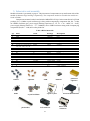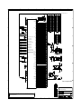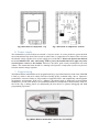
1
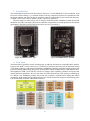
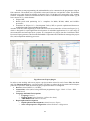
minimodule Wrocław, 17.12.2013 The module along with the documentation have been developed by: Mateusz Cholewiński, Michał Dziergwa, Paweł Kaczmarek, Jan Kędzierski, Marek Wnuk. Department of Fundamental Cybernetics and Robotics, Wrocław University of Technology Wrocław 2013 The documentation consists of this manual and a project created using EAGLE ver. 6.5.0. software from CadSoft. This project can be obtained from the authors of the module. It can be used for educational purposes only. Bilbao is a city in Spain, the capital of the province of Biscay. The population proper is just over 372,000. Nowadays, Bilbao is a vigorous service city that is experiencing an ongoing social, economic, and aesthetic revitalisation process, started by the iconic Bilbao Guggenheim Museum, and continued by infrastructure investments. 2 Contents 1. Introduction ..................................................................................................................................... 5 2. Overview.......................................................................................................................................... 5 3. Features of MK60FX512VLQ15........................................................................................................ 6 4. Clock Distribution ............................................................................................................................ 7 5. Schematic and assembly ................................................................................................................. 8 6. Power supply ................................................................................................................................. 10 7. Programming ................................................................................................................................. 10 8. Connectors and signals .................................................................................................................. 12 Bibliography........................................................................................................................................... 17 3 4 1. Introduction The minimodule described in this document is based on a 32-bit MK60FX512 microcontroller from Freescale’s Kinetis family [1]. It contains all the necessary components required to communicate with the microcontroller and allow the proper operation of the on-board modules (JTAG and USB connector, 50 MHz/32 kHz clock sources, diodes, resistors, capacitors, inductors). The main purpose of this project was to design a small and flexible standalone module that would enable the use of the wide range of K60 microcontroller’s capabilities in a broad spectrum of educational applications. The final version of the board can be seen in Fig 2 and Fig 1. Fig 1 Assembled board - bottom Fig 2 Assembled board - top 2. Overview The Kinetis MCU portfolio consists of multiple pin-, peripheral- and software-compatible MCU families based on the ARM® Cortex™-M4 core [2]. Families are built from innovative 90 nm thin-film storage (TFS) flash technology with unique FlexMemory (EEPROM) capability, and offer industry-leading low power and mixed signal analog integration. The K60 MCU family includes IEEE® 1588 Ethernet, Fulland High-Speed USB 2.0 On-The-Go with device charger detect capability, hardware encryption and tamper detection capabilities. Devices start from 256 KB of flash in 100 LQFP packages extending up to 1 MB in a 256 MAPBGA package with a rich suite of analog, communication, timing and control peripherals. High memory density K60 family devices include an optional single precision floating point unit, NAND flash controller and DRAM controller. 5 3. Features of MK60FX512VLQ15 Operating Characteristics – Voltage range: 1.71 to 3.6 V – Flash write voltage range: 1.71 to 3.6 V – Temperature range (ambient): -40 to 105° C – 128-bit unique identification (ID) number per chip Human-machine interface – Low-power hardware touch sensor interface (TSI) – General-purpose input/output Performance – Up to 150 MHz ARM Cortex-M4 core with DSP instructions delivering 1.25 Dhrystone MIPS per MHz Analog modules – Four 16-bit SAR ADCs – Programmable gain amplifier (PGA) (up to x64) integrated into each ADC – Two 12-bit DACs – Four analog comparators (CMP) containing a 6-bit DAC and programmable reference input – Voltage reference Memories and memory interfaces – Up to 1024 KB program flash memory on non-FlexMemory devices – Up to 512 KB program flash memory on FlexMemory devices – Up to 512 KB FlexNVM on FlexMemory devices – 16 KB FlexRAM on FlexMemory devices – Up to 128 KB RAM – Serial programming interface (EzPort) – FlexBus external bus interface – NAND flash controller interface Timers – Programmable delay block – Two 8-channel motor control/general purpose/PWM timers – Two 2-channel quadrature decoder/general – purpose timers – IEEE 1588 timers – Periodic interrupt timers – 16-bit low-power timer – Carrier modulator transmitter – Real-time clock Clocks – 3 to 32 MHz crystal oscillator – 32 kHz crystal oscillator – Multi-purpose clock generator Communication interfaces – Ethernet controller with MII and RMII interface to external PHY and hardware IEEE 1588 capability – USB high-/full-/low-speed On-theGo controller with ULPI interface – USB high-/full-/low-speed On-theGo controller with on-chip high speed transceiver – USB full-/low-speed On-the-Go controller with on-chip transceiver – USB Device Charger detect – Two Controller Area Network (CAN) modules – Three SPI modules – Two I2C modules – Six UART modules – Secure Digital host controller (SDHC) – Two I2S modules System peripherals – Multiple low-power modes to provide power optimization based on application requirements – Memory protection unit with multimaster protection – 32-channel DMA controller, supporting up to 128 request sources – External watchdog monitor – Software watchdog – Low-leakage wakeup unit Security and integrity modules – Hardware CRC module to support fast cyclic redundancy checks – Hardware random-number generator – Hardware encryption supporting DES, 3DES, AES, MD5, SHA-1, and SHA-256 algorithms 6 4. Clock Distribution The Multipurpose Clock Generator (MCG, [1]) module controls which clock source is used to derive the system clocks. The clock generation logic divides the selected clock source into a variety of clock domains, including the clocks for the system bus masters, system bus slaves, and flash memory. The clock generation logic also implements module-specific clock gating to allow granular shutoff of modules. The primary clocks for the system are generated from the MCGOUTCLK clock. The clock generation circuitry provides several clock dividers that allow different portions of the device to be clocked at different frequencies. This allows for tradeoffs between performance and power dissipation. Various modules, such as the USB OTG Controller, have module-specific clocks that can be generated from the MCGPLLCLK or MCGFLLCLK clock. In addition, there are various other module-specific clocks that have other alternate sources. Clock selection for most modules is controlled by the SOPT registers in the SIM module. The clocking diagram for MCG module can be seen in detail in Fig 3. Fig 3 Clocking diagram In addition to the MCG module, K60 possesses three additional clock modules [1]: Oscillators (OSC) – two high frequency crystal oscillators, which generate filtered oscillator clock signals - OSCCLK for MCU system, OSCERCLK for on-chip peripherals, and OSC32KCLK. On Bilbao Bizkaia minimodule, OSC is omitted and an external 50 MHz crystal oscillator (Q1) and a small set of necessary components is used as a clock source. RTC Oscillator (RTC OSC) – provides a clock source for the Real Time Clock (RTC) module. It is used in conjunction with an external 32 kHz crystal (Q2). The following are a few of the more common clock configurations for this device: Core clock System clock Bus clock FlexBus clock Flash clock Option 1 Option 2 120 MHz 120 MHz 60 MHz 40 MHz 20 MHz 150 MHz 150 MHz 75 MHz 50 MHz 25 MHz 7 5. Schematic and assembly Module schematic is presented on page 9. The placement of components on top and bottom side of the module is shown in Fig 6 and Fig 7 respectively. The components needed to assemble the module are listed in Table 1. Components mounted on the board include: MK60FX512VLQ15 microcontroller in LQFP144 package (U1), a 50Mhz crystal oscillator (Q1) along with accompanying components (R1, R2 – 68 Ω), an 32kMHz oscillator (Q2), power supply filtering capacitors (C1, C2, C3 .. C18 – 100nF, C5 – 22uF), power supply filtering chokes (L1 .. L7 – 100MHz), micro USB B connector along with accompanying components (R4, R5 – 33Ω) and a safety diode D1. Table 1 Bill of materials Qty Parts 1 1 1 2 1 7 12 USB PWR J-LINK SVL, SVR SVT L1, L2, L3, L4, L5, L6, L7 C1, C2, C3, C4, C6, C8, C9, C10, C11, C13, C17, C18 C15 C14, C16 C12 R2 R4, R5 R1, R3 R6 Q1 Q2 U1 D1 J1 1 2 1 1 2 2 1 1 1 1 1 1 resistor diode Value Description SMD LED0603 ML10 100MHz 100nF M0805 C0603 micro USB connector LED 2x5 connector 2x24 pin header 2x13 pin header inductor capacitor 10nF 1uF 22uF 1k 33 68 510 50MHz 32768Hz MK60FX512VLQ15 C0603 C0603 SMC B R0603 R0603 R0603 R0603 DXO-57 2-POLE SMD LQFP144 SOD523 N/A capacitor capacitor polarized capacitor resistor resistor resistor resistor crystal oscillator crystal Freescale Kinetis K60 microcontroler schottky diode ! NOT A PART capacitor LED 2x5 connector 8 polarized capacitor inductor 2-pole crystal crystal oscillator pin headers Package Freescale Kinetis K60 micro USB connector 1 2 3 4 5 6 7 8 PTA[4..17],PTA19,PTA[24..29],PTB[0..11],PTB[16..23],PTC[0..19],PTD[0..15],PTE[0..12],PTE[24..28],GND,VDDA,VREFH,VREFL,VSSA,+5V_USB,VOUT33,ADC0,ADC1,DAC0,DAC1,PGA0_DP,PGA0_DM,PGA1_DP,PGA1_DM,PGA2_DP,PGA2_DM,PGA3_DP,PGA3_DM,USB0_DP,USB0_DM,RESET,V+,CLK SVL VREF_OUT/CMP1_IN5/CMP0_IN5/ADC1_SE18 36 35 ADC0_SE16/CMP1_IN2/ADC0_SE21 ADC1_SE16/CMP2_IN2/ADC0_SE22 DAC0 DAC1 38 39 DAC0_OUT/CMP1_IN3/ADC0_SE23 DAC1_OUT/CMP0_IN4/CMP2_IN3/ADC1_SE23 PGA0_DP PGA0_DM 27 28 PGA0_DP/ADC0_DP0/ADC1_DP3 PGA0_DM/ADC0_DM0/ADC1_DM3 PGA1_DP PGA1_DM 29 30 PGA1_DP/ADC1_DP0/ADC0_DP3 PGA1_DM/ADC1_DM0/ADC0_DM3 PGA2_DP PGA2_DM 23 24 PGA2_DP/ADC2_DP0/ADC3_DP3/ADC0_DP1 PGA2_DM/ADC2_DM0/ADC3_DM3/ADC0_DM1 PGA3_DP PGA3_DM 25 26 PGA3_DP/ADC3_DP0/ADC2_DP3/ADC1_DP1 PGA3_DM/ADC3_DM0/ADC2_DM3/ADC1_DM1 +3V3 100n C10 ADC0 ADC1 GND C USB0_DP USB0_DM 19 20 USB0_DP USB0_DP USB0_DM R2 RESET 1K +3V3 USB0_DM Q2 32768Hz RESET 74 41 40 6 17 44 57 71 93 107 121 134 D VSSA RESET_B EXTAL32 XTAL32 VSS1 VSS2 VSS3 VSS4 VSS5 VSS6 VSS7 VSS8 VSS9 34 VSSA 18 VSSUSB GND PTB0/LLWU_P5 PTB1 PTB2 PTB3 PTB4 PTB5 PTB6 PTB7 PTB8 PTB9 PTB10 PTB11 PTB16 PTB17 PTB18 PTB19 PTB20 PTB21 PTB22 PTB23 81 82 83 84 85 86 87 88 89 90 91 92 95 96 97 98 99 100 101 102 PTB0 PTB1 PTB2 PTB3 PTB4 PTB5 PTB6 PTB7 PTB8 PTB9 PTB10 PTB11 PTB16 PTB17 PTB18 PTB19 PTB20 PTB21 PTB22 PTB23 PTC0 PTC1/LLWU_P6 PTC2 PTC3/LLWU_P7 PTC4/LLWU_P8 PTC5/LLWU_P9 PTC6/LLWU_P10 PTC7 PTC8 PTC9 PTC10 PTC11/LLWU_P1 PTC12 PTC13 PTC14 PTC15 PTC16 PTC17 PTC18 PTC19 103 104 105 106 109 110 111 112 113 114 115 116 117 118 119 120 123 124 125 126 PTC0 PTC1 PTC2 PTC3 PTC4 PTC5 PTC6 PTC7 PTC8 PTC9 PTC10 PTC11 PTC12 PTC13 PTC14 PTC15 PTC16 PTC17 PTC18 PTC19 PTD0/LLWU_P12 PTD1 PTD2/LLWU_P13 PTD3 PTD4/LLWU_P14 PTD5 PTD6/LLWU_P15 PTD7 PTD8 PTD9 PTD10 PTD11 PTD12 PTD13 PTD14 PTD15 127 128 129 130 131 132 133 136 137 138 139 140 141 142 143 144 PTD0 PTD1 PTD2 PTD3 PTD4 PTD5 PTD6 PTD7 PTD8 PTD9 PTD10 PTD11 PTD12 PTD13 PTD14 PTD15 PTE0 PTE1/LLWU_P0 PTE2/LLWU_P1 PTE3 PTE4/LLWU_P2 PTE5 PTE6 PTE7 PTE8 PTE9 PTE10 PTE11 PTE12 PTE24 PTE25 PTE26 PTE27 PTE28 1 2 3 4 7 8 9 10 11 12 13 14 15 45 46 47 48 49 PTE0 PTE1 PTE2 PTE3 PTE4 PTE5 PTE6 PTE7 PTE8 PTE9 PTE10 PTE11 PTE12 PTE24 PTE25 PTE26 PTE27 PTE28 V+ 100MHz 2 4 6 8 10 12 14 16 18 20 22 24 26 PTD11 PTD9 PTD7 PTD5 PTD3 PTD1 PTC19 PTC17 PTC15 PTC13 PTC11 PTC9 C9 C8 B L1 C12 22uF C6 C4 C3 C2 C1 100n 100n 100n 100n 100n 100n 100n GND GND GND GND GND GND GND GND GND L7 d1 D1 +5V_USB 100n 100MHz C11 1u 1 2 3 4 5 R5 USB0_DM 33 100MHz 33 USB0_DP C14 R4 1 2 3 4 5 C L6 GND GND GND L5 L3 VREFL C15 C13 100MHz C17 10n 100n 100n 1u L4 C16 100MHz L2 VREFH 100MHz 100n 100MHz D Q1 1 C18 2 INH VDD 4 VSS OUT 3 R1 EXTAL 68 R3 50MHz GND 68 CLK VOUT33 2 1 J1 Close J1 to supply from USB M. Cholewinski, M. Dziergwa, P. Kaczmarek, J. Kedzierski Wroclaw University of Technology MK60FX512VLQ15 E 1 3 5 7 9 11 13 15 17 19 21 23 25 USB 37 B SVT PTD10 PTD8 PTD6 PTD4 PTD2 PTD0 PTC18 PTC16 PTC14 PTC12 PTC10 PTC8 CLK +3V3 VOUT33 A VSSA 21 PTA19 PTA24 PTA25 PTA26 PTA27 PTA28 PTA29 V+ PTC6 PTC4 PTC2 PTC0 PTB22 PTB20 PTB18 PTB16 PTB10 PTB8 PTB6 PTB4 PTB2 PTB0 PTA28 PTA26 PTA24 PTA19 PTA16 PTA14 PTA12 PTA10 PTA8 VDDA VOUT33 EXTAL 2 4 6 8 10 12 14 16 18 20 22 24 26 28 30 32 34 36 38 40 42 44 46 48 +3V3 VREGIN R6 22 +5V_USB GNDGND PTA4 PTA5 PTA6 PTA7 PTA8 PTA9 PTA10 PTA11 PTA12 PTA13 PTA14 PTA15 PTA16 PTA17 1 3 5 7 9 11 13 15 17 19 21 23 25 27 29 31 33 35 37 39 41 43 45 47 GND PTC7 PTC5 PTC3 PTC1 PTB23 PTB21 PTB19 PTB17 PTB11 PTB9 PTB7 PTB5 PTB3 PTB1 PTA29 PTA27 PTA25 RESET PTA17 PTA15 PTA13 PTA11 PTA9 PWR VBAT +5V_USB VREFL J-LINK PTD12 PTD14 PTE0 PTE2 PTE4 PTE6 PTE8 PTE10 PTE12 USB0_DM +5V_USB PGA2_DM PGA3_DM PGA0_DM PGA1_DM ADC0 DAC1 PTE25 PTE27 PTA4 PTA6 VREFH VDDA GND +3V3 VREFH VREFL 42 VDDA VREFH RESET 2 4 6 8 10 12 14 16 18 20 22 24 26 28 30 32 34 36 38 40 42 44 46 48 +3V3 VDDA 32 33 VREFH VREFL 50 51 52 53 54 55 58 59 60 61 62 63 64 65 66 67 68 69 72 73 75 76 77 78 79 80 SVR 1 3 5 7 9 11 13 15 17 19 21 23 25 27 29 31 33 35 37 39 41 43 45 47 510 31 VDDA PTA0 PTA1 PTA2 PTA3 PTA4/LLWU_P3 PTA5 PTA6 PTA7 PTA8 PTA9 PTA10 PTA11 PTA12 PTA13/LLWU_P4 PTA14 PTA15 PTA16 PTA17 PTA18 PTA19 PTA24 PTA25 PTA26 PTA27 PTA28 PTA29 PTD13 PTD15 PTE1 PTE3 PTE5 PTE7 PTE9 PTE11 USB0_DP VOUT33 PGA2_DP PGA3_DP PGA0_DP PGA1_DP ADC1 DAC0 PTE24 PTE26 PTE28 PTA5 PTA7 VREFL VSSA V+ + K60 VDD1 VDD2 VDD3 VDD4 VDD5 VDD6 VDD7 VDD8 VDD9 1 3 5 7 9 V+ U1 5 16 43 56 70 94 108 122 135 2 4 6 8 10 +3V3 +3V3 +3V3 A JTAG_TMS JTAG_TCK JTAG_TDO JTAG_TDI BILBAO Minimodule Bilbao is a city in Spain, the capital of the province of Biscay. The population proper is just over 372,000. Nowadays, Bilbao is a vigorous service city that is experiencing an ongoing social, economic, and aesthetic revitalisation process, started by the iconic Bilbao Guggenheim Museum, and continued by infrastructure investments. 1 2 3 4 5 6 7 8 E Fig 7 Placement of components - bottom Fig 6 Placement of components - top 6. Power supply The minimodule is powered from an external 3.3V power source. It is also possible to power the K60 microcontroller directly from USB. In order to achieve this, J1 jumper has to be shorted. This will cause the internal voltage regulator to be used to supply power to the MCU. Please note that it is not allowed to exceed 290mA load. Also, when using USB to power the module DO NOT apply any other external power source to the module. Moreover, the MCU peak current consumption can reach 300mA. This means that when the MCU is running at full speed it is impossible to power any devices from the internal voltage regulator. 7. Programming The Bilbao Bizkaia minimodule can be programmed using a specialized interface such as the SEGGER J-Link [6], which is the most widely used line of debug probes available today, due to impressive performance, extensive feature set, large number of supported CPUs, and compatibility with all popular development environments. With up to 3 MBytes/s download speed to RAM and record breaking flashloaders, as well as the ability to set an unlimited number of breakpoints in flash memory of MCUs, the J-Link (Fig 8) debug probes are undoubtedly the best choice to optimize debugging and flash programming experience. Fig 8 Bilbao Bizkaia minimodule connected to J-Link EDU 10 In order to start programming, the minimodule has to be connected to the programmer using an IDC connector. The module uses a 10 pin IDC socket and J-Link uses a 20 pin IDC socket. This dictates the need to use some form of an adapter, as shown in Fig 8. J-Link has to be connected to a PC, running software compatible with Freescale Kinetis MCUs such as CodeWarrior Development Studio [3] (at least version 10.X.), which features: Eclipse IDE, Build system with optimizing C/C++ compilers for RS08, HCS08, ARM, and ColdFire processors, Extensions to Eclipse C/C++ Development Tools (CDT) to provide sophisticated features to troubleshoot and repair embedded applications. Another useful tool when beginning to work with Freescale microcontrollers is Processor Expert [4, 5], which is designed for rapid application development of embedded applications for a wide range of microcontrollers and microprocessor systems. It is integrated as a plug-in into the CodeWarrior IDE. Processor Expert generates code from the Embedded Components and CodeWarrior manages the project files, and compilation and debug processes. Fig 8 Processor Expert plug-in In order to start working with a new project a project creation wizard is used. Choose File, then New and click Bareboard Project. A wizard window will show up where the project name and workspace path can be specified. Then, the following project options need to be configured: Devices: select K60FX512 (150 Mhz), Connections: select (unless using a different programmer) Segger J-Link / J-Trace / SWO (SWD based) Language and Build Tools Options o Language: leave C, o Floating Point: leave Hardware (-mfloat-abi=hard), o ARM Build Tools: select Freescale, Rapid Aplication Development o Rapid Aplication Development: select Processor Expert, o Start with perspective designed for: select Hardware configuration. 11 When a project is created Processor Expert automatically introduces one or more CPU modules. These can be adjusted to the user’s needs via graphical user interface. After the CPU has been initialized, various new components can be added to the project. These are divided into the following categories project (Fig. 9): CPU External Devices – components for devices externally controlled to the CPU. For example sensors, memories, displays or EVM equipment, CPU Internal Peripherals – components using any of on-chip peripherals offered by the CPU, Logical Device Drivers – developed to offer users the Hardware Abstraction Layer (HAL) for bare-metal applications as well as RTOS applications, Operating systems – components related to Processor Expert interaction with operating system running on the target, SW – components encapsulating pure software algorithms or inheriting a hardware-dependent components for accessing peripherals. After double-clicking on the selected component, PE will add it to the current project, and it will show up in the Components tab. Doubleclicking a component added this way will open the configuration window for that module. Importantly, after each change in the module configuration, it has to be built again. Some configuration options Fig 9 PE module categories may be unavailable, depending on how a certain block is set up. Unfortunately, Processor Expert does not allow to change all available registers/fields. In such situations it is advisable to use Peripheral Initialization modules, which provide only initialization configuration of a function block. These modules can be found in the Components library in Processor Internal Peripherals/Peripheral Initialization section. More detailed information on configuring and adding components can be found in [5] (K40 and K60 microcontrollers can be configured using PE in an almost identical manner) 8. Connectors and signals In order to allow the user to utilize the full capabilities of the K60 microcontroller, all the signals have been connected to two row pin headers (SVL, SVT, SVR). This allows for a fast and reliable connection to another, custom designed board. Numbering and spacing of the pins is shown in Fig 10. A detailed description of pins and along with their various functions is presented in Table 2, Table 3 and Table 4. Fig 10 Pin header overview 12 Table 2 SVL Connector 4 Pin Name PTD13 PTD12 PTD15 PTD14 DISABLED DISABLED DISABLED DISABLED 5 PTE1 ADC1_SE5a ADC1_SE5a 6 7 PTE0 PTE3 ADC1_SE4a ADC1_SE7a ADC1_SE4a ADC1_SE7a 8 PTE2 ADC1_SE6a ADC1_SE6a 9 PTE5 DISABLED 10 PTE4 DISABLED 11 20 PTE7 PTE6 PTE9 PTE8 PTE11 PTE10 USB0_DP PTE12 V_OUT33 USB0_DM 21 PGA2_DP 22 +5V_USB 23 PGA3_DP 24 PGA2_DM 25 PGA0_DP 26 PGA3_DM 27 PGA1_DP 28 PGA0_DM 29 ADC1 30 PGA1_DM 31 DAC0 32 ADC0 33 PTE24 34 DAC1 35 36 1 2 3 12 13 14 15 16 17 18 19 Default ALT0 DISABLED DISABLED ADC2_SE17 ADC2_SE16 ADC3_SE16 DISABLED USB0_DP ADC3_SE17 VOUT33 USB0_DM PGA2_DP/ ADC2_DP0/ ADC3_DP3/ ADC0_DP1 USB0_DP ADC3_SE17 VOUT33 USB0_DM PGA2_DP/ ADC2_DP0/ ADC3_DP3/ ADC0_DP1 PGA3_DP/ ADC3_DP0/ ADC2_DP3/ ADC1_DP1 PGA2_DM/ ADC2_DM0/ ADC3_DM3/ ADC0_DM1 PGA0_DP/ ADC0_DP0/ ADC1_DP3 PGA3_DM/ ADC3_DM0/ ADC2_DM3/ ADC1_DM1 PGA1_DP/ ADC1_DP0/ ADC0_DP3 PGA1_DM/ ADC1_DM0/ ADC0_DM3 ADC1_SE16/ CMP2_IN2/ ADC0_SE22 PGA1_DP/ ADC1_DP0/ ADC0_DP3 DAC0_OUT/ CMP1_IN3/ ADC0_SE23 ADC0_SE16/ CMP1_IN2/ ADC0_SE21 ADC0_SE17/ EXTAL1 DAC1_OUT/ CMP0_IN4/ CMP2_IN3/ ADC1_SE23 PGA3_DP/ ADC3_DP0/ ADC2_DP3/ ADC1_DP1 PGA2_DM/ ADC2_DM0/ ADC3_DM3/ ADC0_DM1 PGA0_DP/ ADC0_DP0/ ADC1_DP3 PGA3_DM/ ADC3_DM0/ ADC2_DM3/ ADC1_DM1 PGA1_DP/ ADC1_DP0/ ADC0_DP3 PGA1_DM/ ADC1_DM0/ ADC0_DM3 ADC1_SE16/ CMP2_IN2/ ADC0_SE22 PGA1_DP/ ADC1_DP0/ ADC0_DP3 DAC0_OUT/ CMP1_IN3/ ADC0_SE23 ADC0_SE16/ CMP1_IN2/ ADC0_SE21 ADC0_SE17/ EXTAL1 DAC1_OUT/ CMP0_IN4/ CMP2_IN3/ ADC1_SE23 PTE26 ADC3_SE5b PTE25 ADC0_SE18/ XTAL1 ADC2_SE17 ADC2_SE16 ADC3_SE16 ALT1 PTD13 PTD12 PTD15 PTD14 PTE1/ LLWU_P0 PTE0 PTE3 PTE2/ LLWU_P1 PTE5 PTE4/ LLWU_P2 PTE7 PTE6 PTE9 PTE8 PTE11 PTE10 ALT2 SPI2_SOUT SPI2_SCK SPI2_PCS1 SPI2_SIN ALT3 FTM3_FLT0 ALT4 ALT5 ALT6 SDHC0_D5 SDHC0_D4 SDHC0_D7 SDHC0_D6 FB_A21 FB_A20 FB_A23 FB_A22 ALT7 SPI1_SOUT UART1_RX SDHC0_D0 I2C1_SCL SPI1_SIN SPI1_PCS1 SPI1_SIN UART1_TX UART1_RTS_ b SDHC0_D1 SDHC0_CMD I2C1_SDA RTC_CLKOUT SPI1_SOUT SPI1_SCK UART1_CTS_ b SDHC0_DCLK SPI1_PCS2 UART3_RX SDHC0_D2 SPI1_PCS0 UART3_TX SDHC0_D3 UART3_RTS_ b UART3_CTS_ b UART5_RX UART5_TX UART5_RTS_ b UART5_CTS_ b I2S0_RXD0 I2S0_MCLK I2S0_RX_ BCLK I2S0_RX_FS I2S0_TX_FS I2S0_TXD0 FTM3_CH2 FTM3_CH1 FTM3_CH4 FTM3_CH3 FTM3_CH6 FTM3_CH5 I2S0_TX_ BCLK FTM3_CH7 SPI1_PCS3 I2S0_TXD1 I2S0_RXD1 PTE12 FTM3_CH0 USB_SOF_ OUT PTE24 CAN1_TX UART4_TX I2S1_TX_FS EWM_OUT_b I2S1_RXD1 ADC3_SE5b PTE26 ENET_158 8_ CLKIN UART4_CTS_ b I2S1_TXD0 RTC_CLKOUT USB_CLKIN ADC0_SE18/ XTAL1 PTE25 CAN1_RX UART4_RX I2S1_TX_ BCLK EWM_IN I2S1_TXD1 13 38 PTE28 PTE27 ADC3_SE7a ADC3_SE4b 39 PTA5 DISABLED PTA5 ULPI_DIR FTM0_CH4 I2S1_RX_ BCLK ULPI_CLK FTM0_CH3 I2S1_RXD0 37 ADC3_SE7a ADC3_SE4b PTE28 PTE27 40 PTA4 41 PTA7 NMI_b/ EZP_CS_b ADC0_SE10 ADC0_SE10 PTA4/ LLWU_P3 PTA7 42 PTA6 ADC3_SE6a ADC3_SE6a PTA6 43 VREFL VREFH VSSA VDDA V+ GND VREFL VREFH VSSA VDDA VREFL VREFH VSSA VDDA 44 45 46 47 48 TSI0_CH5 UART4_RTS_ b USB_CLKIN FTM0_CH2 I2S1_MCLK RMII0_RXER/ MII0_RXER CMP2_ OUT I2S0_TX_ BCLK FTM0_CH1 JTAG_TRST_ b NMI_b TRACE_D3 TRACE_ CLKOUT Table 3 SVT Connector Pin Name Default ALT0 ALT1 ALT2 ALT3 ALT4 PTD10 DISABLED PTD10 2 PTD11 DISABLED PTD11 SPI2_PCS0 UART5_CTS_ b 3 PTD8 DISABLED PTD8 I2C0_SCL UART5_RX 4 PTD9 DISABLED PTD9 I2C0_SDA UART5_TX PTD6/ LLWU_P15 SPI0_PCS3 UART0_RX FTM0_CH6 PTD7 CMT_IRO UART0_TX FTM0_CH7 ADC0_SE6b PTD5 SPI0_PCS2 ADC0_SE5b PTD2/ PTD3 PTD0/ PTD1 SPI0_SOUT SPI0_SIN SPI0_PCS0 SPI0_SCK PTD6 ADC0_SE7b 6 PTD7 DISABLED 7 PTD4 8 PTD5 ADC0_SE6b PTD2 10 PTD3 11 PTD0 12 PTD1 DISABLED DISABLED DISABLED ADC0_SE5b 9 ADC0_SE7b UART5_RTS_ b UART0_CTS_b/ UART0_COL_ b UART2_RX UART2_TX UART2_RTS_ b UART2_CTS_ b SDHC0_ CLKIN FTM0_CH5 FTM3_CH2 FTM3_CH3 FTM3_CH0 FTM3_CH1 PTC18 DISABLED PTC18 UART3_RTS_ b ENET0_1588 _ TMR2 14 PTC19 DISABLED PTC19 UART3_CTS_ b ENET0_1588 _ TMR3 15 PTC16 DISABLED PTC16 CAN1_RX UART3_RX ENET0_1588 _ TMR0 16 PTC17 DISABLED PTC17 CAN1_TX UART3_TX ENET0_1588 _ TMR1 PTC14 PTC15 19 PTC12 20 PTC13 DISABLED DISABLED DISABLED DISABLED PTC14 PTC15 PTC12 PTC13 18 21 PTC10 22 PTC11 23 PTC8 24 PTC9 25 CLK ---- 26 ADC1_SE6b UART4_RX UART4_TX UART4_RTS_ b UART4_CTS_ b ADC1_SE6b PTC10 I2C1_SCL FTM3_CH6 I2S0_RX_FS ADC1_SE7b ADC1_SE7b PTC11/ LLWU_P11 I2C1_SDA FTM3_CH7 I2S0_RXD1 ADC1_SE4b/ CMP0_IN2 ADC1_SE5b/ CMP0_IN3 ADC1_SE4b/ CMP0_IN2 ADC1_SE5b/ CMP0_IN3 PTC8 FTM3_CH4 I2S0_MCLK PTC9 FTM3_CH5 I2S0_RX_ BCLK 14 ALT7 FB_A19 FB_A16/ NFC_CLE FB_A17/ NFC_ALE 13 17 ALT6 FB_A18/ NFC_RE 1 5 ALT5 FB_AD0 FTM0_FLT0 FTM0_FLT1 FB_AD1/ NFC_DATA0 FB_AD4 FB_AD3 FB_ALE/ FB_CS0_b FB_TBST_b/ FB_CS2_b/ FB_BE15_8_b FB_CS3_b/ FB_BE7_0_b FB_CS5_b/ FB_TSIZ1/ FB_BE23_16_b FB_CS4_b/ FB_TSIZ0/ FB_BE31_24_b FB_AD25 FB_AD24 FB_AD27 FB_AD26 FB_AD5/ NFC_DATA2 FB_RW_b/ NFC_WE FB_AD7/ NFC_DATA4 FB_AD6/ NFC_DATA3 EWM_OUT_b I2S1_RX_FS I2S1_RX_ BCLK I2S1_RXD1 I2S1_RXD0 NFC_CE1_b FB_TA_b NFC_RB NFC_CE0_b FTM3_FLT0 I2S1_MCLK FTM2_FLT0 ADC0_SE5b Table 4 SVR Connector 2 Pin Name GND V+ 3 PTC7 CMP0_IN1 CMP0_IN1 PTC7 SPI0_SIN USB_SOF_ OUT I2S0_RX_FS FB_AD8/ NFC_DATA5 4 PTC6 CMP0_IN0 CMP0_IN0 PTC6/ LLWU_P1 0 SPI0_SOUT PDB0_EXTRG I2S0_RX_ BCLK FB_AD9/ NFC_DATA6 5 PTC5 DISABLED PTC5/ SPI0_SCK LPTMR0_ ALT2 I2S0_RXD0 6 PTC4 DISABLED PTC4/ SPI0_PCS0 UART1_TX FTM0_CH3 CMP1_IN1 CMP1_IN1 PTC3/ LLWU_P7 SPI0_PCS1 UART1_RX FTM0_CH2 CLKOUT I2S0_TX_ BCLK ADC0_SE4b/ CMP1_IN0/ TSI0_CH15 ADC0_SE15/ TSI0_CH14 ADC0_SE14/ TSI0_CH13 ADC0_SE4b/ CMP1_IN0/ TSI0_CH15/ ADC0_SE15/ TSI0_CH14 ADC0_SE14/ TSI0_CH13 PTC2 SPI0_PCS2 UART1_CTS_ b FTM0_CH1 FB_AD12/ NFC_DATA9 I2S0_TX_FS PTC1/ LLWU_P6 SPI0_PCS3 UART1_RTS_ b FTM0_CH0 FB_AD13/ I2S0_TXD0 1 7 PTC3 8 PTC2 9 PTC1 10 PTC0 11 PTB23 12 Default ALT0 ALT1 ALT2 ALT3 PTC0 SPI0_PCS4 PDB0_EXTRG DISABLED PTB23 SPI2_SIN SPI0_PCS5 PTB22 DISABLED PTB22 SPI2_SOUT 13 PTB21 ADC2_SE5a ADC2_SE5a PTB21 SPI2_SCK 14 PTB20 ADC2_SE4a ADC2_SE4a PTB20 SPI2_PCS0 15 PTB19 TSI0_CH12 TSI0_CH12 PTB19 CAN0_RX FTM2_CH1 16 PTB18 TSI0_CH11 TSI0_CH11 PTB18 CAN0_TX FTM2_CH0 PTB17 PTB16 19 PTB11 TSI0_CH10 TSI0_CH9 ADC1_SE15 TSI0_CH10 TSI0_CH9 ADC1_SE15 PTB17 PTB16 PTB11 SPI1_SIN SPI1_SOUT SPI1_SCK UART0_TX UART0_RX UART3_TX PTB10 ADC1_SE14 17 18 ADC1_SE14 PTB10 SPI1_PCS0 UART3_RX PTB9 22 PTB8 23 PTB7 24 PTB6 DISABLED DISABLED ADC1_SE13 ADC1_SE12 SPI1_PCS1 UART3_CTS_ b UART3_RTS_ b ADC1_SE13 ADC1_SE12 PTB9 PTB8 PTB7 PTB6 25 PTB5 ADC1_SE11 ADC1_SE11 PTB5 26 PTB4 ADC1_SE10 ADC1_SE10 PTB4 27 PTB3 28 PTB2 29 PTB1 30 PTB0 31 38 PTA29 PTA28 PTA27 PTA26 PTA25 PTA24 RESET PTA19 ADC0_SE13/ TSI0_CH8 ADC0_SE12/ TSI0_CH7 ADC0_SE9/ ADC1_SE9/ ADC2_SE9/ ADC3_SE9/ TSI0_CH6 ADC0_SE8/ ADC1_SE8/ ADC2_SE8/ ADC3_SE8/ TSI0_CH0 ADC2_SE12 ADC2_SE13 ADC2_SE14 ADC2_SE15 CMP3_IN5 CMP3_IN4 RESET_b XTAL0 ADC0_SE13/ TSI0_CH8 ADC0_SE12/ TSI0_CH7 ADC0_SE9/ ADC1_SE9/ ADC2_SE9/ ADC3_SE9/ TSI0_CH6 ADC0_SE8/ ADC1_SE8/ ADC2_SE8/ ADC3_SE8/ TSI0_CH0 ADC2_SE12 ADC2_SE13 ADC2_SE14 ADC2_SE15 CMP3_IN5 CMP3_IN4 RESET_b XTAL0 39 PTA17 ADC1_SE17 ADC1_SE17 20 21 32 33 34 35 36 37 40 PTA16 CMP3_IN2 CMP3_IN2 ALT4 I2S0_TX_FS I2S0_TX_ BCLK I2S1_TXD1 I2S1_TXD0 I2S1_TX_FS I2S1_TX_ BCLK ALT5 FB_AD10/ NFC_DATA7 FB_AD11/ NFC_DATA8 FB_AD14/ NFC_DATA11 FB_AD28/ NFC_DATA12 FB_AD29/ NFC_DATA13 FB_AD30/ NFC_DATA14 FB_AD31/ NFC_DATA15 FB_OE_b ALT6 I2S0_MCLK CMP0_OUT I2S1_TX_FS CMP1_OUT I2S1_TX_ BCLK I2S0_TXD1 CMP3_OUT CMP2_OUT CMP1_OUT CMP0_OUT FTM2_QD_ PHA FB_AD16 FB_AD17 FB_AD18 EWM_OUT_b EWM_IN FTM0_FLT2 FB_AD19 FTM0_FLT1 FB_AD20 FB_AD21 FB_AD22 FB_AD23 ENET0_1588 _ TMR3 ENET0_1588 _ TMR2 ENET0_1588 _ TMR1 ENET0_1588 _ TMR0 FTM2_FLT0 FTM1_FLT0 I2C0_SDA UART0_CTS_b/ UART0_COL_ b PTB2 I2C0_SCL UART0_RTS_ b PTB1 I2C0_SDA FTM1_CH1 RMII0_MDC/ MII0_MDC FTM1_QD_ PHB PTB0/ I2C0_SCL FTM1_CH0 RMII0_MDI/ MII0_MDIO FTM1_QD_ PHA PTA29 PTA28 PTA27 PTA26 PTA25 PTA24 ULPI_DATA7 ULPI_DATA6 ULPI_DATA5 ULPI_DATA4 ULPI_DATA3 ULPI_DATA2 MII0_COL MII0_TXER MII0_CRS MII0_TXD3 MII0_TXCLK MII0_TXD2 FB_A24 FB_A25 FB_A26 FB_A27 FB_A28 FB_A29 FTM_CLKIN1 RMII0_TXD1/ MII0_TXD1 RMII0_TXD0/ MII0_TXD0 LPTMR0_ ALT1 PTA17 PTA16 FTM1_FLT0 SPI0_SIN UART0_RTS_ b SPI0_SOUT UART0_CTS_b/ UART0_COL_ b 15 ADC2_SE4a FTM2_QD_ PHB FB_AD15 PTB3 PTA19 ALT7 FTM0_FLT0 FTM0_FLT3 I2S0_MCLK I2S0_RX_FS I2S0_RXD1 41 PTA15 CMP3_IN1 CMP3_IN1 PTA15 SPI0_SCK UART0_RX 42 PTA14 CMP3_IN0 CMP3_IN0 UART0_TX PTA13 CMP2_IN1 CMP2_IN1 PTA14 PTA13/ LLWU_P4 SPI0_PCS0 43 CAN0_RX FTM1_CH1 44 PTA12 CMP2_IN0 CMP2_IN0 PTA12 CAN0_TX FTM1_CH0 ADC3_SE15 ADC3_SE4a ADC3_SE5a ADC0_SE11 ADC3_SE15 ADC3_SE4a ADC3_SE5a ADC0_SE11 PTA11 PTA10 PTA9 PTA8 ULPI_DATA1 ULPI_DATA0 ULPI_STP ULPI_NXT FTM2_CH1 FTM2_CH0 FTM1_CH1 FTM1_CH0 PTA11 46 PTA10 47 PTA9 48 PTA8 45 16 RMII0_TXEN/ MII0_TXEN RMII0_CRS_ RMII0_RXD0/ MII0_RXD0 RMII0_RXD1/ MII0_RXD1 MII0_RXCLK MII0_RXD2 MII0_RXD3 I2S1_RX_FS I2S0_RXD0 I2S0_RX_ BCLK I2S0_TXD1 I2S0_TX_FS FTM1_QD_ PHB I2S0_TXD0 FTM1_QD_ PHA FTM2_QD_ PHB FTM2_QD_ PHA FTM1_QD_ PHB FTM1_QD_ PHA TRACE_D0 TRACE_D1 TRACE_D2 Bibliography [1] K60 Sub-Family Reference Manual, K60P144M150SF3RM, Freescale Semiconductor, Inc. 2011. [2] K60 Family Product Brief, K60PB, Freescale Semiconductor, Inc. 2011. [3] CodeWarrior Development Studio for Microcontrollers V10.x Getting Started Guide, Freescale Semiconductor, Inc. 2011. [4] CodeWarrior for Microcontrollers V10.x Processor Expert User Manual, Freescale Semiconductor, Inc. 2011. [5] J. Kędzierski, M. Wnuk, Programowanie mikrokontrolera z rodziny Kinetis K40 w środowisku CodeWarrior Development Studio, Wrocław 2013 [6] J-Link / J-Trace User Guide, UM08001, SEGGER Microcontroller GmbH & Co. KG, 2013. 17