1
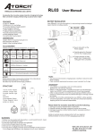
v1.19
Table of Contents
1. Introduction
2. Warranty
3. Features
4. Technical Support
5. Hardware Information
1. Connector Pin-out
2. Building an External Display
6. Selected POST Codes
1. AMI BIOS
2. Quadtel BIOS / PhoenixBIOS Q3.07
3. PhoenixBIOS 4.0 Release 6.0
4. Award BIOS 4.51PG
5. MR BIOS 3.4x
7. Information Resources
1
1. Introduction:
The PST44 is a P.O.S.T (Power On Self Test) diagnostics card for the ISA bus.
It monitors port 80H and displays the data on two 7-segment LED displays. The
PST44 is designed for use in computers with a 286 or later processor since these use
port 80H as their POST port. The card also includes 4 LEDs to indicate if the
power supplies are supplying current. These LEDs simply indicate the presence or
absence of voltage; they do not actually indicate whether the voltage is within
specifications.
A DB-15 connector on the card's back-plane provides access to the 7-segment
data pins if desired. Using this connector, it is possible to connect an external cable
and display for easy viewing of the POST codes.
When the computer's power is turned on, the BIOS performs a series of system
tests before the operating system is loaded. This series of tests is referred to as the
Power On Self Test, or POST. This series of tests typically checks the memory,
disk controllers, keyboard, video card, and a number of other things. If all goes
well, then the computer moves on to loading the operating system. If a major
problem occurs and the computer hangs up, then we need some feedback to tell us
where the problem occurred. The POST card provides this feedback.
As the BIOS steps through each test it must perform, it writes a numeric code to
port 80H. The POST card detects this code, latches it, and displays it. If the system
passes the test, then the code will remain visible for only a short period of time
before being replaced by the code for the next test. If the computer hangs up, then
the code for the failed test is left on the display, indicating where the problem
occurred. The computer technician must then consult a reference table for that
particular brand of BIOS and see what area of hardware the POST code refers to.
This manual includes POST code tables for American Megatrends, Quadtel,
Phoenix, and MR BIOS. Other less popular codes can be obtained from Internet
sites (see the Information Resources section of this manual).
Package Contents
The package you received should contain 2 items:
1. This manual
2. The PST44 P.O.S.T diagnostics card
Disclaimer
The PST44 is not intended or designed for use in military, medical, or other lifecritical applications. Winford Engineering shall not be held responsible or liable for
damages or injury that occur as a result of the use this product.
2
2. Warranty:
Winford Engineering provides a 2-year warranty for the PST44 P.O.S.T. card.
This warranty does not cover the misuse or abuse of this product. In the event of
product failure, Winford Engineering should be contacted for information regarding
the return and replacement of the product.
3
3. Features:
Works with 8 or 16-bit ISA bus.
Monitors port 80 hexadecimal (standard for AT machines).
Has voltage-present indicators** on the +5, -5, +12, -12 supply lines.
Has a DB-15 connector on the back which allows the connection of an external
display.
** These LEDs simply indicate the presence of voltage on the supply lines. They do
not verify that it is within the required specifications. For example, the LED on the
+12 volt supply line will light up even if the supply is only 8 volts at the time.
These indicators simply indicate that some voltage is present.
4
4. Technical Support:
If you find yourself in need of technical assistance beyond what is covered in this
manual, there are several ways to contact Winford Engineering. If your problem is
not urgent, we would prefer that you use e-mail or fax. Please provide us with your
preferred e-mail address, as well as phone/fax numbers where you wish to be
reached. This will help us get back to you in a timely fashion.
NOTE: We cannot provide information about obscure POST codes. We do
provide the common BIOS code definitions in this manual. We also
provide Internet links to POST code lists in the Information Resources
section of this manual.
Technical Support Contacts
Phone: 1-989-671-2941
FAX: 1-989-671-2941
E-mail: [email protected]
Winford Engineering
Technical Support
4169 Four Mile Road
Bay City, MI 48706
5
5. Hardware Information:
5.1 Connector Pin-out
The outputs of the LED display driver chips are brought out via the DB-15
connector on the back of the card. This connector can be used to display the POST
codes on an external display (not provided). This provides convenient access to the
codes if the card itself is not in a position to be viewed. The outputs are active-low
(meant for a common anode 7-segment display). The outputs are brought out before
any current-limiting resistors, so these will need to be built into any external display.
The outputs for the upper display digit (most significant) are denoted with a 'U'
prefix in the table below. The lower digit is indicated with an 'L' prefix.
Pin
Function
1
U_a
2
U_b
3
U_c
4
U_d
5
U_e
6
U_f
7
U_g
8
GND
9
L_a
10
L_b
11
L_c
12
L_d
13
L_e
14
L_f
15
L_g
6
5.2 Building an External Display
It is a simple task to build your own external display for the POST card. You
need a battery (typically a 9-volt), two common-anode 7-segment displays, and
some current-limiting resistors. A schematic is shown below.
a
f
g
e
b
c
d
7
6. Selected POST Codes
Each BIOS manufacturer defines their own POST codes. Therefore, you need a
list of BIOS code definitions from your manufacturer. Each manufacturer also has
more than one version of BIOS, so check that as well. POST codes for some
common BIOS versions are listed below. If your BIOS is not listed, check the
Information Resources section of the manual for links to more POST code lists.
6.1 AMI Code Definitions
CODE
AMI DESCRIPTION
00
System configuration is displayed. Going to give control to INT 19h boot
loader.
01
Processor register test about to start, and NMI to be disabled.
02
NMI is DIsabled. Power on delay starting.
03
Power on delay complete. Any initialization before keyboard BAT is in
progress.
04
Any initialization before keyboard BAT is complete. Reading keyboard
SYS bit, to check soft reset/ power-on.
05
Soft reset/ power-on determined. Going to enable ROM. i.e. disable
shadow RAM/Cache if any.
06
ROM is enabled. Calculating ROM BIOS checksum, and waiting for KB
controller input buffer to be free.
07
ROM BIOS checksum passed, KB controller I/B free. Going to issue the
BAT command to keyboard controller.
08
BAT command to keyboard controller is issued. Going to verify the BAT
command.
09
Keyboard controller BAT result verified. Keyboard command byte to be
written next.
0A
Keyboard command byte code is issued. Going to write command byte
data.
0B
Keyboard controller command byte is written. Going to issue Pin-23,24
blocking/unblocking command.
0C
Pin-23,24 of keyboard controller is blocked/ unblocked. NOP command
of keyboard controller to be issued next.
8
CODE
AMI DESCRIPTION
0D
NOP command processing is done. CMOS shutdown register test to be
done next.
0E
CMOS shutdown register R/W test passed. Going to calculate CMOS
checksum, and update DIAG byte.
0F
CMOS checksum calculation is done, DIAG byte written. CMOS init. to
begin (If "INIT CMOS IN EVERY BOOT IS SET").
10
CMOS initialization done (if any). CMOS status register about to init for
Date and Time.
11
CMOS Status register initialized. Going to disable DMA and Interrupt
controllers.
12
DMA controller #1,#2, interrupt controller #1,#2 disabled. About to
disable Video display and init port-B.
13
Video display is disabled and port-B is initialized. Chipset init/ auto
memory detection about to begin.
14
Chipset initialization/ auto memory detection over. 8254 timer test about
to start.
15
CH-2 timer test halfway. 8254 CH-2 timer test to be complete.
16
CH-2 timer test over. 8254 CH-1 timer test to be complete.
17
CH-1 timer test over. 8254 CH-0 timer test to be complete.
18
CH-0 timer test over. About to start memory refresh.
19
Memory Refresh started. Memory Refresh test to be done next.
1A
Memory Refresh line is toggling. Going to check 15 micro second
ON/OFF time.
1B
Memory Refresh period 30 micro second test complete. Base 64K
memory test about to start.
20
Base 64k memory test started. Address line test to be done next.
21
Address line test passed. Going to do toggle parity.
22
Toggle parity over. Going for sequential data R/W test.
23
Base 64k sequential data R/W test passed. Any setup before Interrupt
vector init about to start.
24
Setup required before vector initialization complete. Interrupt vector
initialization about to begin.
9
CODE
AMI DESCRIPTION
25
Interrupt vector initialization done. Going to read I/O port of 8042 for
turbo switch (if any).
26
I/O port of 8042 is read. Going to initialize global data for turbo switch.
27
Global data initialization is over. Any initialization after interrupt vector
to be done next.
28
Initialization after interrupt vector is complete. Going for monochrome
mode setting.
29
Monochrome mode setting is done. Going for Color mode setting.
2A
Color mode setting is done. About to go for toggle parity before optional
rom test.
2B
Toggle parity over. About to give control for any setup required before
optional video ROM check.
2C
Processing before video ROM control is done. About to look for optional
video ROM and give control.
2D
Optional video ROM control is done. About to give control to do any
processing after video ROM returns control.
2E
Return from processing after the video ROM control. If EGA/VGA not
found then do display memory R/W test.
2F
EGA/VGA not found. Display memory R/W test about to begin.
30
Display memory R/W test passed. About to look for the retrace checking.
31
Display memory R/W test or retrace checking failed. About to do
alternate Display memory R/W test.
32
Alternate Display memory R/W test passed. About to look for the
alternate display retrace checking.
33
Video display checking over. Verification of display type with switch
setting and actual card to begin.
34
Verification of display adapter done. Display mode to be set next.
35
Display mode set complete. BIOS ROM data area about to be checked.
36
BIOS ROM data area check over. Going to set cursor for power on
message.
37
Cursor setting for power on message id complete. Going to display the
power on message.
38
Power on message display complete. Going to read new cursor positon.
10
CODE
AMI DESCRIPTION
39
New cursor position read and saved. Going to display the reference
string.
3A
Reference string display is over. Going to display the Hit <ESC>
message.
3B
Hit <ESC> message displayed. Virtual mode memory test about to start.
40
Preparation for virtual mode test started. Going to verify from video
memory.
41
Returned after verifying from display memory. Going to prepare the
descriptor tables.
42
Descriptor tables prepared. Goin to enter in virtual mode for memory
test.
43
Entered in the virtual mode. Going to enable interrupts for diagnostics
mode.
44
Interrupts enabled (if diagnostics switch is on). Going to initialize data to
check memory wrap around at 0:0.
45
Data initialized. Going to check for memory wrap around at 0:0 and
finding the total system memory size.
46
Memory wrap around test done. Memory size calculation over. About to
go for writing patterns to test memory.
47
Pattern to be tested written in extended memory. Going to write patterns
in base 640k memory.
48
Patterns written in base memory. Going to find out amount of memory
below 1M memory.
49
Amount of memory below 1M found and verified. Going to find out
amount of memory above 1M memory.
4A
Amount of memory above 1M found and verified. Going for BIOS ROM
data area check.
4B
BIOS ROM data area check over. Going to check <ESC> and to clear
memory below 1M for soft reset.
4C
Memory below 1M cleared. (SOFT RESET) Going to clear memory
above 1M.
4D
Memory above 1M cleared. (SOFT RESET) Going to save the memory
size.
11
CODE
AMI DESCRIPTION
4E
Memory test started. (NO SOFT RESET) About to display the first 64k
memory test.
4F
Memory size display started. This will be updated during memory test.
Going for sequential and random memory test.
50
Memory test below 1M complete. Going to adjust memory size for
relocation/ shadow.
51
Memory size adjusted due to relocation/ shadow. Memory test above 1M
to follow.
52
Memory test above 1M complete. Going to prepare to go back to real
mode.
53
CPU registers are saved including memory size. Going to enter in real
mode.
54
Shutdown successful, CPU in real mode. Going to restore registers saved
during preparation for shutdown.
55
Registers restored. Going to disable gate A20 address line.
56
A20 address line disable successful. BIOS ROM data area about to be
checked.
57
BIOS ROM data area check halfway. BIOS ROM data area check to be
complete.
58
BIOS ROM data area check over. Going to clear Hit <ESC> message.
59
Hit <ESC> message cleared. <WAIT...> message displayed. About to
start DMA and interrupt controller test.
60
DMA page register test passed. About to verify from display memory.
61
Display memory verification over. About to go for DMA #1 base register
test.
62
DMA #1 base register test passed. About to go for DMA #2 base register
test.
63
DMA #2 base register test passed. About to go for BIOS ROM data area
check.
64
BIOS ROM data area check halfway. BIOS ROM data area check to be
complete.
65
BIOS ROM data area check over. About to program DMA unit 1 and 2.
66
DMA unit 1 and 2 programming over. About to initialize 8259 interrupt
controller.
12
CODE
AMI DESCRIPTION
67
8259 initialization over. About to start keyboard test.
80
Keyboard test started. clearing output buffer, checking for stuck key,
About to issue keyboard reset command.
81
Keyboard reset error/stuck key found. About to issue keyboard controller
interface test command.
82
Keyboard controller interface test over. About to write command byte
and init circular buffer.
83
Command byte written, Global data init done. About to check for lockkey.
84
Lock-key checking over. About to check for memory size mismatch with
CMOS.
85
Memory size check done. About to display soft error and check for
password or bypass setup.
86
Password checked. About to do programming before setup.
87
Programming before setup complete. Going to CMOS setup program.
88
Returned from CMOS setup program and screen is cleared. About to do
programming after setup.
89
Programming after setup complete. Going to display power on screen
message.
8A
First screen message displayed. About to display <WAIT...> message
8B
<WAIT...> message displayed. About to do Main and Video BIOS
shadow.
8C
Main and Video BIOS shadow successful. Setup options programming
after CMOS setup about to start.
8D
Setup options are programmed, mouse check and init to be done next.
8E
Mouse check and initialization complete. Going for hard disk, floppy
reset.
8F
Floppy check returns that floppy is to be initialized. Floppy setup to
follow.
90
Floppy setup is over. Test for hard disk presence to be done.
91
Hard disk presence test over. Hard disk setup to follow.
92
Hard disk setup complete. About to go for BIOS ROM data area check.
13
CODE
AMI DESCRIPTION
93
BIOS ROM data area check halfway. BIOS ROM data area check to be
complete.
94
BIOS ROM data area check over. Going to set base and extended
memory size.
95
Memory size adjusted due to mouse support, hdisk type-47. Going to
verify from display memory.
96
Returned after verifying from display memory. Going to do any init
before C800 optional ROM control
97
Any init before C800 optional ROM control is over. Optional ROM
check and control will be done next.
98
Optional ROM control is done. About to give control to do any required
processing after optional ROM returns control.
99
Any initialization required after optional ROM test over. Going to setup
timer data area and printer base address.
9A
Return after setting timer and printer base address. Going to set the RS232 base address.
9B
Returned after RS-232 base address. Going to do any initialization before
Co-processor test
9C
Required initialization before co-processor is over. Going to initialize the
coprocessor next.
9D
Coprocessor initialized. Going to do any initialization after Co-processor
test.
9E
Initialization after co-processor test is complete. Going to check extd
keyboard, keyboard ID and num-lock.
9F
Extd keyboard check is done, ID flag set. num-lock on/off. Keyboard ID
command to be issued.
A0
Keyboard ID command issued. Keyboard ID flag to be reset.
A1
Keyboard ID flag reset. Cache memory test to follow.
A2
Cache memory test over. Going to display any soft errors.
A3
Soft error display complete. Going to set the keyboard typematic rate.
A4
Keyboard typematic rate set. Going to program memory wait states.
A5
Memory wait states programming over. Screen to be cleared next.
A6
Screen cleared. Going to enable parity and NMI.
14
CODE
AMI DESCRIPTION
A7
NMI and parity enabled. Going to do any initialization required before
giving control to optional ROM at E000.
A8
Initialization before E000 ROM control over. E000 ROM to get control
next.
A9
Returned from E000 ROM control. Going to do any initialization
required after E000 optional ROM control.
AA
Initialization after E000 optional ROM control is over. Going to display
the system configuration.
15
6.2 Quadtel BIOS / PhoenixBIOS Q3.07 Code Definitions
This list of POST codes applies only to Quadtel BIOS or PhoenixBIOS Q3.07 on
an AT-class computer. Please note that different BIOS versions may have different
code definitions and that some versions of BIOS may have codes which are OEMspecific.
CODE
QUADTEL / PHOENIX Q3.07 DESCRIPTION
02
CPU Flags test
04
CPU Register test
06
Initialize system hardware
08
Initialize chip set registers
0A
Perform BIOS checksum test
0C
Test DMA page registers
0E
Test 8254 timers
10
Initialize 8254 timers
12
Test both 8237 DMA controllers
14
Initialize 8237 DMA controllers
16
Initialize 8259, Reset coprocessor
18
Test 8259 interrupt controller registers
1A
Verify refresh is occurring
1C
Base 64K address test
1E
Base 64K ram test (16 bits)
20
Upper 16 of 32 bit test failed
22
Test 8742 keyboard controller
24
Verify CMOS / Configure CMOS
26
Verify/Load NVRAM parameters
28
Protected mode 1
2A
AutoSize memory chips
2C
Activate interleave (if possible)
2E
Exit 1st protected mode test
30
Unexpected shutdown
16
CODE
QUADTEL / PHOENIX Q3.07 DESCRIPTION
32
Determine system board memory size
34
Relocate memory option
36
Configure EMS memory option
38
Configure Wait State option
3A
Retest 64K base ram
3C
Determine relative CPU speed
3E
Get switches/jumper status from 8742
40
Configure CPU speed
42
Initialize interrupt vectors
44
Verify video configuration
46
Initialize video system
48
Test for unexpected interrupts
4A
Start 2nd protected mode test
4C
Perform LDT instruction test
4E
Perform TR instruction test
50
Perform LSL instruction test
52
Perform LAR instruction test
54
Perform VERR instruction test
56
Unexpected exception
58
Perform A20 gate test
5A
Keyboard ready test
5C
Determine if AT or XT keyboard type
5E
Enter third protected mode test
60
Base memory test
62
Base memory address test
64
Shadow memory test
66
Extended memory test
68
Extended address test
6A
Determine memory size
17
CODE
QUADTEL / PHOENIX Q3.07 DESCRIPTION
6C
Display error messages
6E
Configure ROM/RAM BIOS
70
System timer test
72
Real time clock test
74
Test for stuck keys
76
Initialize hardware interrupt vectors
78
Detect and test coprocessor
7A
Determine/init COM channels
7C
Determine LPT channels
7E
Initialize BIOS Data Area
80
Detect floppy controller
82
Test floppy drives
84
Fixed disk test
86
Perform external ROM scan
88
Test keylock/keyboard type
8A
Wait for F1 test
8C
Final system initialization
8E
Interrupt 19 boot loader
B0
Unknown interrupt occurred
18
6.3 PhoenixBIOS 4.0 Release 6.0 Code Definitions
This list of POST codes applies to PhoenixBIOS 4.0 Release 6.0. Please note
that different BIOS versions may have different code definitions and that some
versions of BIOS may have codes which are OEM-specific.
CODE
PHOENIX 4.0 DESCRIPTION
02
Verify Real Mode
03
Disable Non- Maskable Interrupt (NMI)
04
Get CPU type
06
Initialize system hardware
08
Initialize chipset with initial POST values
09
Set IN POST flag
0A
Initialize CPU registers
0B
Enable CPU cache
0C
Initialize caches to initial POST values
0E
Initialize I/ O component
0F
Initialize the local bus IDE
10
Initialize Power Management
11
Load alternate registers with initial POST values
12
Restore CPU control word during warm boot
13
Initialize PCI Bus Mastering devices
14
Initialize keyboard controller
16
BIOS ROM checksum
17
Initialize cache before memory autosize
18
8254 timer initialization
1A
8237 DMA controller initialization
1C
Reset Programmable Interrupt Controller
20
Test DRAM refresh
22
Test 8742 Keyboard Controller
24
Set ES segment register to 4 GB
19
CODE
PHOENIX 4.0 DESCRIPTION
26
Enable A20 line
28
Autosize DRAM
29
Initialize POST Memory Manager
2A
Clear 512 KB base RAM
2C
RAM failure on address line xxxx *
2E
RAM failure on data bits xxxx * of low byte of memory bus
2F
Enable cache before system BIOS shadow
30
RAM failure on data bits xxxx * of high byte of memory bus
32
Test CPU bus- clock frequency
33
Initialize Phoenix Dispatch Manager
36
Warm start shut down
38
Shadow system BIOS ROM
3A
Autosize cache
3C
Advanced configuration of chipset registers
3D
Load alternate registers with CMOS values
42
Initialize interrupt vectors
45
POST device initialization
46
Check ROM copyright notice
48
Check video configuration against CMOS
49
Initialize PCI bus and devices
4A
Initialize all video adapters in system
4B
QuietBoot start (optional)
4C
Shadow video BIOS ROM
4E
Display BIOS copyright notice
50
Display CPU type and speed
51
Initialize EISA board
52
Test keyboard
54
Set key click if enabled
58
Test for unexpected interrupts
20
CODE
PHOENIX 4.0 DESCRIPTION
59
Initialize POST display service
5A
Display prompt "Press F2 to enter SETUP"
5B
Disable CPU cache
5C
Test RAM between 512 and 640 KB
60
Test extended memory
62
Test extended memory address lines
64
Jump to UserPatch1
66
Configure advanced cache registers
67
Initialize Multi Processor APIC
68
Enable external and CPU caches
69
Setup System Management Mode (SMM) area
6A
Display external L2 cache size
6B
Load custom defaults (optional)
6C
Display shadow- area message
6E
Display possible high address for UMB recovery
70
Display error messages
72
Check for configuration errors
76
Check for keyboard errors
7C
Set up hardware interrupt vectors
7E
Initialize coprocessor if present
80
Disable onboard Super I/ O ports and IRQs
81
Late POST device initialization
82
Detect and install external RS232 ports
83
Configure non- MCD IDE controllers
84
Detect and install external parallel ports
85
Initialize PC- compatible PnP ISA devices
86
Re-initialize onboard I/O ports.
87
Configure Motherboard Configurable Devices (optional)
88
Initialize BIOS Data Area
21
CODE
PHOENIX 4.0 DESCRIPTION
89
Enable Non- Maskable Interrupts (NMIs)
8A
Initialize Extended BIOS Data Area
8B
Test and initialize PS/ 2 mouse
8F
Determine number of ATA drives (optional)
90
Initialize hard- disk controllers
91
Initialize local- bus hard- disk controllers
92
Jump to UserPatch2
93
Build MPTABLE for multi- processor boards
95
Install CD ROM for boot
96
Clear huge ES segment register
97
Fixup Multi Processor table
98
Search for option ROMs. One long, two short beeps on checksum failure
99
Check for SMART Drive (optional)
9A
Shadow option ROMs
9C
Set up Power Management
9D
Initialize security engine (optional)
9E
Enable hardware interrupts
9F
Determine number of ATA and SCSI drives
A0
Set time of day
A2
Check key lock
A4
Initialize Typematic rate
A8
Erase F2 prompt
AA
Scan for F2 key stroke
AC
Enter SETUP
AEh
Clear Boot flag
B0
Check for errors
B2
POST done - prepare to boot operating system
B4
1 One short beep before boot
B5
Terminate QuietBoot (optional)
22
CODE
PHOENIX 4.0 DESCRIPTION
B6
Check password (optional)
B9
Prepare Boot
BA
Initialize DMI parameters
BB
Initialize PnP Option ROMs
BC
Clear parity checkers
BD
Display MultiBoot menu
BE
Clear screen (optional)
BF
Check virus and backup reminders
C0
Try to boot with INT 19
C1
Initialize POST Error Manager (PEM)
C2
Initialize error logging
C3
Initialize error display function
C4
Initialize system error handler
C5
PnPnd dual CMOS (optional)
C6
Initialize notebook docking (optional)
C7
Initialize notebook docking late
C8
Force check (optional)
C9
Extended checksum (optional)
D2
Unknown interrupt
*If the BIOS detects eror 2C, 2E, or 30, it displays 2 additional codes on the display
which indicate the failed address lines or bits. It first displays the error code,
followed by a pause, then the high-order byte, another pause, and then the low-order
byte. For example, the code '2C 0002' means that address line 1 has failed. It would
be displayed as '2C' (pause) '00' (pause) '02'.
23
CODE
PHOENIX 4.0 (FOR BOOT BLOCK IN FLASH ROM)
E0
Initialize the chipset
E1
Initialize the bridge
E2
Initialize the CPU
E3
Initialize system timer
E4
Initialize system I/ O
E5
Check force recovery boot
E6
Checksum BIOS ROM
E7
Go to BIOS
E8
Set Huge Segment
E9
Initialize Multi Processor
EA
Initialize OEM special code
EB
Initialize PIC and DMA
EC
Initialize Memory type
ED
Initialize Memory size
EE
Shadow Boot Block
EF
System memory test
F0
Initialize interrupt vectors
F1
Initialize Run Time Clock
F2
Initialize video
F3
Initialize System Management Mode
F4
Output one beep before boot
F5
Boot to Mini DOS
F6
Clear Huge Segment
F7
Boot to Full DOS
24
6.4 AwardBIOS Version 4.51PG Code Definitions
This list of POST codes applies AwardBIOS 4.51PG. Please note that different
BIOS versions may have different code definitions and that some versions of BIOS
may have codes which are OEM-specific.
CODE
AWARD 4.51PG DESCRIPTION
01
Processor test 1; Processor status verification
02
Processor test 2; Read/Write and verify all CPU registers
03
Initialize chips; Disable NMI, PIE, AIE, UEI, SQWV. Disable video,
parity checking, DMA. Reset math coprocessor. Clear all page registers,
CMOS shutdown byte. Initialize DMA controller 0 and 1. Initialize
interrupt controllers 0 and 1.
04
Test memory refresh toggle
05
Blank video, initialize keyboard; Keyboard controller initialization
06
Reserved
07
Test CMOS interface and battery
08
Set up low memory; Early chipset initialization, memory presence test,
OEM chipset routines, clear low 64K memory, test first 64K memory
09
Early cache initialization; Cyrix CPU specific, CPU and cache
initialization
0A
Set up interrupt vector table; Initialize first 120 interrupt vectors
0B
Test CMOS RAM checksum
0C
Initialize keyboard; Detect the type of keyboard controller
0D
Initialize video interface; Detect CPU clock, read CMOS location 14h
to find the type of video in use, detect and initialize video adapter
0E
Test video memory; Write sign-on message to screen, setup shadow
RAM
0F
Test DMA controller 0; BIOS checksum test, keyboard detect and
initialization
10
Test DMA controller 1
11
Test DMA page registers
12-13 Reserved
14
Test Timer Counter 2
25
CODE
AWARD 4.51PG DESCRIPTION
15
Test 8259-1 mask bits
16
Test 8259-2 mask bits
17
Test stuck 8259 interrupt bits
18
Test 8259 interrupt functionality
19
Test stuck NMI bits (parity I/O check)
1A
Benchmark; Display CPU clock
1B-1E Reserved
1F
Set EISA mode
20
Enable slot 0; System board
21-2F Enable slots 1-15
30
Size base and extended memory; Size the base memory from 256K to
640K and the extended memory above 1MB
31
Test base and extended memory; Test the base memory from 256K to
640K and the extended memory above 1MB using various bit patterns
32
Test EISA extended memory
33-3B Reserved
3C
Setup enabled
3D
Initialize and install mouse if present
3E
Setup cache controller
3F
Reserved
40
Display virus protect disable or enable
41
Initialize floppy drive and controller
42
Initialize hard drive and controller
43
Detect & initialize serial & parallel ports
44
Reserved
45
Detect and initialize math coprocessor
46
Reserved
47
Reserved
48-4D Reserved
26
CODE
AWARD 4.51PG DESCRIPTION
4E
Manufacturing POST loop or display messages
4F
Security check
50
Write CMOS; Write CMOS back to RAM and clear screen
51
Pre-boot enable; Enable parity checking, enable NMI, enable cache
before boot
52
Initialize option ROMs; Initialize any option ROMs present from C800h
to EFFFFh.
NOTE: When FSCAN option is enabled, ROMs initialize from C8000h
to F7FFFh.
53
Initialize time value
60
Setup virus protect
61
Set boot speed
62
Setup NumLock
63
Boot attempt
B0
Spurious
B1
Unclaimed NMI
BE
Chipset default initialization; Program chipset registers with power-on
BIOS defaults.
BF
Chipset initialization
C0
Turn off chipset cache; OEM specific - Cache control
C1
Memory presence test; OEM specific - Test to size on-board memory
C5
Early shadow; OEM specific - Early shadow enable for fast boot
C6
Cache presence test; External cache-size detection test
E1-EF Setup pages
FF
Boot loader
27
6.5 MR BIOS Version 3.4x Code Definitions
This list of POST codes applies MR BIOS version 3.4x. Please note that
different BIOS versions may have different code definitions and that some versions
of BIOS may have codes which are OEM-specific.
CODE
MR BIOS 3.4x DESCRIPTION
00
Cold Start, output EDX register to I/O ports 85h, 86h, 8Dh, 8Eh for later
use.
01
Initialize any Custom KBD controller, disable CPU cache, cold initialize
onboard I/O chipset, size & test RAM, size cache.
02
Disable critical IO (monitor, DMA, FDC, I/O ports, Speaker, NMI)
03
Checksum the BIOS ROM.
04
Test page registers
05
Enable A20 Gate, issue 8042 SelfTest
06
Initialize ISA I/O
07
Warm initialize custom KBD controller, warm initialize onboard I/O
chipset.
08
Refresh toggle test
09
Test DMA Master registers, test DMA Slave registers.
0A
Test 1st 64K of base memory
0B
Test Master 8259 mask, test Slave 8259 mask
0C
Test 8259 Slave, test 8259 slave's interrupt range, initialize interrupt
vectors 00 - 77h, init KBD buffer variables.
0D
Test Timer0, 8254 channel0
0E
Test 8254 Ch2, speaker channel
0F
Test RTC, CMOS RAM read/write test
10
Turn on Monitor, Show any possible error messages
11
Read and checksum the CMOS
12
Call Video ROM initialization routines, Show Display sign-on message,
Show ESC Delay message
13
Set 8MHz AT-Bus
14
Size and test the base memory, Stuck NMI check
28
CODE
MR BIOS 3.4x DESCRIPTION
15
No KB and PowerOn: Retry KB init
16
Size and test CPU Cache
17
Test A20 OFF and ON states
18
Size and test External memory, Stuck NMI check
19
Size and test System memory, Stuck NMI check
1A
Test RTC Time
1B
Determine Serial Ports
1C
Determine Parallel Ports
1D
Initialize Numeric Coprocessor
1E
Determine Floppy Diskette Controllers
1F
Determine IDE Controllers
20
Display CMOS configuration changes
21
Clear screens
22
Set/reset Numlock LED, perform Security functions
23
Final determination of onboard Serial/Parallel ports
24
Set KB Typematic Rate
25
Initialize Floppy Controller
26
Initialize ATA discs
27
Set the video mode for primary adapter
28
Cyrix WB-CPU support, Green PC: purge 8259 slave, relieve any trapped
IRRs before enabling PwrMgmt, set 8042 pins, Ctrl-Alt-Del possible
now, Enable CPU Features
29
Reset A20 to OFF, install Adapter ROMs
2A
Clear Primary Screen, Convert RTC to system ticks, Set final DOS timer
variables
2B
Enable NMI and latch.
2C
Reserved
2D
Reserved
2E
Fast A20: Fix A20
29
CODE
MR BIOS 3.4x DESCRIPTION
2F
Purge 8259 slave; relieve any trapped IRRs before enabling Green-PC.
Pass control to INT 19 boot
32
Test CPU Burst
33
Reserved
34
Determine 8042, Set 8042 Warm-Boot flag STS.2
35
Test HMA Wrap, Verify A20 enabled via F000:10 HMA
36
Reserved
37
Validate CPU: CPU Step NZ, CPUID Check. Disable CPU features
38
Set 8042 pins (Hi-Speed, Cache-off)
39
PCI Bus: Load PCI; Processor Vector init'd, BIOS Vector init'd, OEM
Vector init'd
3A
Scan PCI Bus
3B
Initialize PCI Bus with intermediate defaults
3C
Initialize PCI OEM with intermediate defaults, OEM bridge
3D
PCI Bus or PLUGnPLAY: Initialize AT Slotmap from AT-Bus CDE
usage
3E
Find phantom CDE ROM PCI-cards
3F
PCI Bus: final Fast-Back-to-Back state
40
OEM POST Initialization, Hook Audio
41
Allocate I/O on PCI-Bus, logs-in PCI-IDE
42
Hook PCI-ATA chips
43
Allocate IRQs on the PCI Bus
44
Allocate/enable PCI Memory/ROM space
45
Determine PS/2 Mouse
46
Map IRQs to PCI Bus per user CMOS, Enable ATA IRQs.
47
PCI-ROM install, note user CMOS
48
If Setup conditions: execute setup utility
49
Test F000 Shadow integrity, Transfer EPROM to Shadow-RAM
4A
Hook VL ATA Chip
4B
Identify and spin-up all drives
30
CODE
MR BIOS 3.4x DESCRIPTION
4C
Detect Secondary IRQ, if VL/AT-Bus IDE exists but its IRQ not known
yet, then autodetect it
4D
Detect/log 32-bit I/O ATA devices
4E
Atapi drive M/S bitmap to Shadow-RAM, Set INT13 Vector
4F
Finalize Shadow-RAM variables
50
Chain INT 13
51
Load PnP, Processor Vector init'd, BIOS Vector init'd, OEM Vector init'd
52
Scan PLUGnPLAY, update PnP Device Count
53
Supplement IRQ usage -- AT IRQs
54
Conditionally assign everything PnP wants
58
Perform OEM Custom boot sequence just prior to INT 19 boot
59
Return from OEM custom boot sequence. Pass control to INT 19 boot
5A
Display MR BIOS logo
88
Dead motherboard and/or CPU and/or BIOS ROM.
FF
BIOS POST Finished.
31
7. Information Resources:
Here are some links to POST codes on the web. Check around for others.
-Huge list of codes (many BIOS types)
http://www.unicore.com
-Phoenix / Award / Quadtel
http://www.phoenix.com/pcuser/
-Microid Research (MR BIOS)
http://www.mrbios.com/postcode.html
-American Megatrends (AMI)
http://www.ami.com/support/bios.html
-Miscellaneous BIOS codes -- these links point to some rather extensive lists
http://webenet.net/~ntuser/
ftp://rtfm.mit.edu/pub/usenet-by-group/news.answers/pc-hardwarefaq/part4
32