Download POST Error Code

Transcript
P801 – PC Debug Card
User’s Manual
TRADEMARK
All products and company names are trademarks or registered
trademarks of their respective holders.
These specifications are subject to change without notice.
Copyright Notice
This document is copyrighted, 2002. All rights are reserved. The
original manufacturer reserves the right to make improvements to
the products described in this manual at any time without notice.
No part of this manual may be reproduced, copied, translated, or
transmitted in any form or by any means without the prior written
permission of the original manufacturer. Information provided in
this manual is intended to be accurate and reliable. However, the
original manufacturer assumes no responsibility for its use, nor for
any infringements upon the rights of third parties which may result
from its use.
Acknowledgements
Award trademarks of Award software Inc.
Phoenix trademarks of Phoenix Technologies Ltd.
AMI trademarks of American Megatrends Inc.
All other product names or trademarks are properties of their
respective owners.
P801-Debug Card
1
P801- 2 LED
P801- 4 LED
P801- M 4 LED
P801-Debug Card
2
1. On board Display “ DP1/DP2”,
2. Optional “DP3/DP4” on the reverse side. or pin header on front side.
3.
4.
PCI RST, VCC +5V, VCC +12V, VCC 3VSB LED Display
P801 board will be to detect “PCICLK”, some board (P4) have to disable
BIOS manual item “Frequency/Voltage Control - Auto Detect PCI CLK”
POST Error Code
BIOS6.00 Revision 1.0
NOTE:
POST (hex)
CFh
C0h
C1h
C3h
C5h
01h
02h
03h
04h
05h
06h
07h
08h
09h
P801-Debug Card
EISA POST codes are typically output to port address 300h
ISA POST codes are output to port address 80h
Description
Test CMOS R/W functionality.
Early chipset initialization:
-Disable shadow RAM
-Disable L2 cache (socket 7 or below)
-Program basic chipset registers
Detect memory
-Auto-detection of DRAM size, type and ECC.
-Auto-detection of L2 cache (socket 7 or below)
Expand compressed BIOS code to DRAM
Call chipset hook to copy BIOS back to E000 & F000 shadow
RAM.
Expand the Xgroup codes locating in physical address 1000:0
Reserved
Initial Superio_Early_Init switch.
Reserved
1. Blank out screen
2. Clear CMOS error flag
Reserved
1. Clear 8042 interface
2. Initialize 8042 self-test
1. Test special keyboard controller for Winbond 977 series Super
I/O chips.
2. Enable keyboard interface.
Reserved
3
POST (hex)
0Ah
0Bh
0Ch
0Dh
0Eh
0Fh
10h
11h
12h
13h
14h
15h
16h
17h
18h
19h
1Ah
1Bh
1Ch
1Dh
1Eh
1Fh
20h
21h
22h
23h
24h
25h
P801-Debug Card
Description
1. Disable PS/2 mouse interface (optional).
2. Auto detect ports for keyboard & mouse followed by a port &
interface swap (optional).
3. Reset keyboard for Winbond 977 series Super I/O chips.
Reserved
Reserved
Reserved
Test F000h segment shadow to see whether it is R/W-able or not. If
test fails, keep beeping the speaker.
Reserved
Auto detect flash type to load appropriate flash R/W codes into the
run time area in F000 for ESCD & DMI support.
Reserved
Use walking 1’s algorithm to check out interface in CMOS
circuitry. Also set real-time clock power status, and then check
for override.
Reserved
Program chipset default values into chipset. Chipset default
values are MODBINable by OEM customers.
Reserved
Initial onboard clock generator if Early_Init_Onboard_Generator
is defined. See also POST 26h.
Reserved
Detect CPU information including brand, SMI type (Cyrix or
Intel) and CPU level (586 or 686).
Reserved
Reserved
Initial interrupts vector table. If no special specified, all H/W
interrupts are directed to SPURIOUS_INT_HDLR & S/W
interrupts to SPURIOUS_soft_HDLR.
Reserved
Initial EARLY_PM_INIT switch.
Reserved
Load keyboard matrix (notebook platform)
Reserved
HPM initialization (notebook platform)
Reserved
1. Check validity of RTC value:
e.g. a value of 5Ah is an invalid value for RTC minute.
2. Load CMOS settings into BIOS stack. If CMOS checksum fails,
use default value instead.
Prepare BIOS resource map for PCI & PnP use. If ESCD is valid,
take into consideration of the ESCD’s legacy information.
Early PCI Initialization:
-Enumerate PCI bus number.
-Assign memory & I/O resource
-Search for a valid VGA device & VGA BIOS, and put it into
C000:0
4
POST (hex)
26h
27h
28h
29h
2Ah
2Bh
2Ch
2Dh
2Eh
2Fh
30h
31h
32h
33h
34h
35h
36h
37h
38h
39h
3Ah
3Bh
3Ch
3Dh
3Eh
3Fh
40h
41h
42h
43h
44h
45h
46h
47h
48h
P801-Debug Card
Description
1. If Early_Init_Onboard_Generator is not defined Onboard clock
generator initialization. Disable respective clock resource to
empty PCI & DIMM slots.
2. Init onboard PWM
3. Init onboard H/W monitor devices
Initialize INT 09 buffer
Reserved
1. Program CPU internal MTRR (P6 & PII) for 0-640K memory
address.
2. Initialize the APIC for Pentium class CPU.
3. Program early chipset according to CMOS setup. Example:
onboard IDE controller.
4. Measure CPU speed.
Reserved
Invoke Video BIOS
Reserved
1. Initialize double-byte language font (Optional)
2. Put information on screen display, including Award title, CPU
type, CPU speed, full screen logo.
Reserved
Reserved
Reserved
Reserved
Reserved
Reset keyboard if Early_Reset_KB is defined e.g. Winbond 977
series Super I/O chips. See also POST 63h.
Reserved
Test DMA Channel 0
Reserved
Test DMA Channel 1.
Reserved
Test DMA page registers.
Reserved
Reserved
Test 8254
Reserved
Test 8259 interrupt mask bits for channel 1.
Reserved
Test 8259 interrupt mask bits for channel 2.
Reserved
Reserved
Test 8259 functionality.
Reserved
Reserved
Reserved
Initialize EISA slot
Reserved
5
POST (hex)
49h
4Ah
4Bh
4Ch
4Dh
4Eh
4Fh
50h
51h
52h
53h
54h
55h
56h
57h
58h
59h
5Ah
5Bh
5Ch
5Dh
5Eh
5Fh
60h
61h
62h
63h
64h
65h
66h
67h
68h
69h
6Ah
P801-Debug Card
Description
1. Calculate total memory by testing the last double word of each
64K page.
2. Program write allocation for AMD K5 CPU.
Reserved
Reserved
Reserved
Reserved
1. Program MTRR of M1 CPU
2. Initialize L2 cache for P6 class CPU & program CPU with
proper cacheable range.
3. Initialize the APIC for P6 class CPU.
4. On MP platform, adjust the cacheable range to smaller one in
case the cacheable ranges between each CPU are not identical.
Reserved
Initialize USB Keyboard & Mouse.
Reserved
Test all memory (clear all extended memory to 0)
Clear password according to H/W jumper (Optional)
Reserved
Display number of processors (multi-processor platform)
Reserved
1. Display PnP logo
2. Early ISA PnP initialization
-Assign CSN to every ISA PnP device.
Reserved
Initialize the combined Trend Anti-Virus code.
Reserved
(Optional Feature)
Show message for entering AWDFLASH.EXE from FDD
(optional)
Reserved
1. Initialize Init_Onboard_Super_IO
2. Initialize Init_Onbaord_AUDIO.
Reserved
Reserved
Okay to enter Setup utility; i.e. not until this POST stage can users
enter the CMOS setup utility.
Reserved
Reserved
Reset keyboard if Early_Reset_KB is not defined.
Reserved
Initialize PS/2 Mouse
Reserved
Prepare memory size information for function call:
INT 15h ax=E820h
Reserved
Turn on L2 cache
Reserved
6
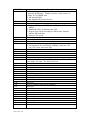
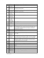
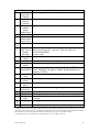
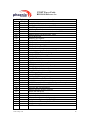
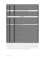
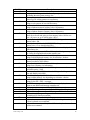
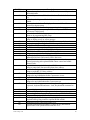
POST (hex)
6Bh
6Ch
6Dh
6Eh
6Fh
70h
71h
72h
73h
74h
75h
76h
77h
78h
79h
7Ah
7Bh
7Ch
7Dh
7Eh
7Fh
80h
81h
82h
83h
84h
85h
86h
87h
88h
89h
8Ah
P801-Debug Card
Description
Program chipset registers according to items described in Setup &
Auto-configuration table.
Reserved
1. Assign resources to all ISA PnP devices.
2. Auto assign ports to onboard COM ports if the corresponding
item in Setup is set to “AUTO”.
Reserved
1. Initialize floppy controller
2. Set up floppy related fields in 40:hardware.
Reserved
Reserved
Reserved
(Reserved
Reserved
Detect & install all IDE devices: HDD, LS120, ZIP, CDROM…..
(Optional Feature)
Enter AWDFLASH.EXE if:
-AWDFLASH.EXE is found in floppy drive.
-ALT+F2 is pressed.
Detect serial ports & parallel ports.
Reserved
Reserved
Detect & install co-processor
Reserved
Init HDD write protect.
Reserved
Reserved
Switch back to text mode if full screen logo is supported.
-If errors occur, report errors & wait for keys
-If no errors occur or F1 key is pressed to continue:
wClear EPA or customization logo.
Reserved
Reserved
E8POST.ASM starts
1. Call chipset power management hook.
2. Recover the text fond used by EPA logo (not for full screen logo)
3. If password is set, ask for password.
Save all data in stack back to CMOS
Initialize ISA PnP boot devices
1. USB final Initialization
2. Switch screen back to text mode
Reserved
NET PC: Build SYSID Structure.
Reserved
1. Assign IRQs to PCI devices
2. Set up ACPI table at top of the memory.
Reserved
7
POST (hex)
8Bh
8Ch
8Dh
8Eh
8Fh
90h
91h
92h
93h
94h
95h
96h
FFh
Description
1. Invoke all ISA adapter ROMs
2. Invoke all PCI ROMs (except VGA)
Reserved
1. Enable/Disable Parity Check according to CMOS setup
2. APM Initialization
Reserved
Clear noise of IRQs
Reserved
Reserved
Reserved
Read HDD boot sector information for Trend Anti-Virus code
1. Enable L2 cache
2. Program Daylight Saving
3. Program boot up speed
4. Chipset final initialization.
5. Power management final initialization
6. Clear screen & display summary table
7. Program K6 write allocation
8. Program P6 class write combining
Update keyboard LED & typematic rate
1. Build MP table
2. Build & update ESCD
3. Set CMOS century to 20h or 19h
4. Load CMOS time into DOS timer tick
5. Build MSIRQ routing table.
Boot attempt (INT 19h)
POST Error Code
BIOS4.51G Revision 1.0
NOTE:
EISA POST codes are typically output to port address 300h
ISA POST codes are output to port address 80h
Description
OEM specific-cache control
POST (hex)
C0
Turn off
chipset Cache
1
Processor Processor status (1FLAGS) Verification.
Test1
Tests the following processor status fllages:
Carry, zero, sign, overflow, The BIOS sets each flag, verifies
they are set, then turns each flag off and verifies it is off.
2
Processor
Test2
P801-Debug Card
Read / Write / Verify all CPU registers, except ss , sp, andbp
with date
pattern FF and 00
8
POST (hex)
3
Initialize
Chips
4
5
6
7
BE
C1
C5
C6
8
9
A
B
C
D
E
F
10
11
12
13
Description
Disable NMI, PIE, AIE, UEI, SQWV
Disable Video, parity checking, DMA Reset mach coprocessor,
Clear all page registers, CMOS shutdown byte Initialize timer 0,
1, and 2, including set EISA timer to a known state Initialize
DMA controllers 0 and 1.Initialize interrupt controllers 0 and
1Initialize EISA extended registers.
Test Memory RAM must be periodically refreshed to keep the memory from
Refresh
decaying. This function is working properly.
Toggle
Blank video,
Initialize
keyboard
Reserved
Test CMOS
Interface and
Battery Status
Chipset
default
Initialization
Memory
presence Test
Early shadow
Cache
presence
Setup low
memory
Early Cache
Initialization
Setup
Interrupt
Vector Table
Test CMOS
RAM
Checksum
Initialize
keyboard
Initialize
Video
Test Video
Memory
Test DMA
Controller 0
Test DMA
Controller 1
Test DMA
page registers
Reserved
Reserved
P801-Debug Card
keyboard controller initialization.
Reserved
Verifies CMOS is working correctly, detects bad battery.
Programming chipset Register with power on BIOS defaults.
OEM specific – Test to size on-board memory.
OEM Specific – Early shadow enable for fast boot.
External cache size detection test .
Early chip set initialization memory presence test OEM chip set
routines, Clear low 64k of memory, Test first 64k memory.
Cyrix CPU initialization, Cache Initialization.
Initialize first 120 interrupt vectors with SPURIOUS – INT – H
DLR
and initialize INT 00h-1Fh according to INT – TBL
Test CMOS RAM Chceksum, if bad, or insert key pressed, load
defaults.
Detect type of keyboard controller(optional) Set NUM – COCK
status.
Detect CPU clock, Read CMOS location 14h to find out, Type
of video in use. Detect and Initialize Video Adapter.
Test video memory, write sign – on message to screen, Setup
shadow RAM – Enable shadow According to Setup.
BIOS checksum test. keyboard detect and initialization.
Test DMA Page registers.
Reserved
Reserved
9
POST (hex)
Description
14
Test Timer Test 8254 Timer 0 Counter 2.
Counter 2
15 Test 8259-1 Verify 8259 channel 1 masked interrupts by alternately turning
MASK Bits off and on the interrupt lines.
16
Test 8259-2
MASK Bits
17
Test Stuck
8259
Interrupts
18
Test 8259
Interrupt
Functionality
19
Test Stuck
NMI
Bits(Parity /
IO Check)
1A Display CPU
clock
1B - Reserved
1E
1F
Set EISA
Mode
Verify 8259 channel 2 masked interrupts by alternately turning
off and on the interrupt lines.
Turn off interrupt then verify no interrupt is on.
Force an interrupt and verify the Interrupt occurred.
Verify NMI can be cleared.
Display CPU clock
Reserved
If EISA non – volatile memory checksum is good, execute
EISA initialization, if not, execute ISA tests an clear EISA node
flag. Test EISA Configuration Memory Integrity ( checksum a
communication Interface ).
20 Enable Slot 0 Initialize slot 0 ( system board ).
21 – Enable Slots Initialize slots 1 through 15
2F
1 – 15
30 Size Base and size base memory form 256k to 640k and extended memory
Extended above 1MB.
Memory
31 Test Base and Test base memory from 256k to 640k and extended memory
Extended above 1MB Using various patterns. NOTE : This test is skipped
Memory
in EISA mode and can be skipped with ESC key in ISA mode.
32
Test EISA If EISA Mode flag is set then test EISA memory found is slots
Initialization. NOTE : This test is skipped in ISA mode and can
be skipped with ESC key in ISA mode.
33 –
Reserved Reserved
3B
3C Setup Enabled Setup Enabled
3D
Initialize & Detect if mouse is present, initialize mouse, install interrupt
Install Mouse vectors.
3E Setup Cache Initialize cache controller.
Controller
3F
Reserved Reserved
BF
Chipset
Program chipset registers with setup values
Initialization
40
Display
Display virus protect disable or Enable
P801-Debug Card
10
POST (hex)
41
Initialize
Floppy Drive
Controller
42 Initialize Hard
Drive &
Controller
43
Detect &
Initialize
Serial /
Parallel Ports
44
Reserved
45
Detect &
Initialize Math
Coprocessor
46 –
Reserved
4D
4E Manufacturing
POST Loop or
Display
Messages
4F
Security
Check
50 Write CMOS
51
Pre – boot
Enable
52
Initialize
Option ROMs
53
60
61
62
63
B0
B1
E1
-EF
FF
Description
Initialize floppy disk controller and any drives.
Initialize hard disk controller and drives.
Initialize any serial and parallel posts ( also game port ).
Reserved
Initialize math coprocessor
Reserved
Reboot if Manufacturing POST Loop pin is set. Otherwise
display any messages (I, e,. any non – fatal error that were
detected during POST)
and enter setup.
Ask password security ( optional ) .
Write all CMOS values back to RAM and clear screen.
Enable parity checker, Enable NMI, Enable cache before boot.
Initialize any option ROMs present from C8000h to EFFFFh
NOTE : When FSCAN option is Enabled, ROMs initialize form
C8000h to E7FFFh.
Initialize Time Initialize time value in 40h : BIOS area.
value
Setup Virus Setup virus protect according to Setup.
Protect
Setup Boot Set system speed for boot
Speed
Setup
Setup NumLock status according to setup.
Num Lock
Boot Attempt Set low stack Boot via INT 19h
Spurious
If interrupt occurs in protected
Unclaimed If unmasked NMI occurs, display Press F1 to disable F1 NMI,
NMI
F2 reboot.
Setup Pages E1 – Page 2, etc.
Boot
Boot
★ The information in this document is subject to change without notice, and should not be considered as a
commitment by Award. Although Award will make every effort to inform users of substantive errors, Award
disclaims all liability for any loss or damage resulting from the use of this document or any hardware or software
described herein, including without limitation contingent, special, or incidental liability.
Copyright1999 by Award Software International, Inc. All rights reserved.
P801-Debug Card
11
POST Error Code
BIOS4.00 Release 6.x.
POST (hex)
Code
Beeps
02h
03h
04h
06h
07h
08h
09h
0Ah
0Bh
0Ch
0Eh
0Fh
10h
11h
12h
13h
14h
16h
1-2-2-3
17h
18h
1Ah
1Ch
20h
1-3-1-1
22h
1-3-1-3
24h
28h
29h
2Ah
2Ch
1-3-4-1
2Eh
1-3-4-3
2Fh
32h
33h
36h
38h
3Ah
3Ch
3Dh
41h
42h
45h
P801-Debug Card
Description
Verify Real Mode
Disable Non-Maskable Interrupt (NMI)
Get CPU type
Initialize system hardware
Disable shadow and execute code from the ROM.
Initialize chipset with initial POST values
Set IN POST flag
Initialize CPU registers
Enable CPU cache
Initialize caches to initial POST values
Initialize I/O component
Initialize the local bus IDE
Initialize Power Management
Load alternate registers with initial POST values
Restore CPU control word during warm boot
Initialize PCI Bus Mastering devices
Initialize keyboard controller
BIOS ROM checksum
Initialize cache before memory Auto size
8254 timer initialization
8237 DMA controller initialization
Reset Programmable Interrupt Controller
Test DRAM refresh
Test 8742 Keyboard Controller
Set ES segment register to 4 GB
Auto size DRAM
Initialize POST Memory Manager
Clear 512 kB base RAM
RAM failure on address line xxxx*
RAM failure on data bits xxxx* of low byte of memory bus
Enable cache before system BIOS shadow
Test CPU bus-clock frequency
Initialize Phoenix Dispatch Manager
Warm start shut down
Shadow system BIOS ROM
Auto size cache
Advanced configuration of chipset registers
Load alternate registers with CMOS values
Initialize extended memory for RomPilot
Initialize interrupt vectors
POST device initialization
12
POST (hex)
Code
Beeps
46h
2-1-2-3
47h
48h
49h
4Ah
4Bh
4Ch
4Eh
4Fh
50h
51h
52h
54h
55h
58h
2-2-3-1
59h
5Ah
5Bh
5Ch
60h
62h
64h
66h
67h
68h
69h
6Ah
6Bh
6Ch
6Eh
70h
72h
76h
7Ch
7Dh
7Eh
80h
81h
81h
83h
84h
85h
86h
87h
88h
89h
8Ah
P801-Debug Card
Description
Check ROM copyright notice
Initialize I20 support
Check video configuration against CMOS
Initialize PCI bus and devices
Initialize all video adapters in system
QuietBoot start (optional)
Shadow video BIOS ROM
Display BIOS copyright notice
Initialize MultiBoot
Display CPU type and speed
Initialize EISA board
Test keyboard
Set key click if enabled
Enable USB devices
Test for unexpected interrupts
Initialize POST display service
Display prompt "Press F2 to enter SETUP"
Disable CPU cache
Test RAM between 512 and 640 kB
Test extended memory
Test extended memory address lines
Jump to UserPatch1
Configure advanced cache registers
Initialize Multi Processor APIC
Enable external and CPU caches
Setup System Management Mode (SMM) area
Display external L2 cache size
Load custom defaults (optional)
Display shadow-area message
Display possible high address for UMB recovery
Display error messages
Check for configuration errors
Check for keyboard errors
Set up hardware interrupt vectors
Initialize Intelligent System Monitoring
Initialize coprocessor if present
Disable onboard Super I/O ports and IRQs
Late POST device initialization
Detect and install external RS232 ports
Configure non-MCD IDE controllers
Detect and install external parallel ports
Initialize PC-compatible PnP ISA devices
Re-initialize onboard I/O ports.
Configure Motherboard Configurable Devices(optional)
Initialize BIOS Data Area
Enable Non-Maskable Interrupts (NMIs)
Initialize Extended BIOS Data Area
13
POST (hex)
Code
Beeps
8Bh
8Ch
8Fh
90h
91h
92h
93h
95h
96h
97h
98h
1-2
99h
9Ah
9Ch
9Dh
9Eh
9Fh
A0h
A2h
A4h
A8h
AAh
ACh
AEh
B0h
B1h
B2h
B4h
B5h
B6h
B7h
B9h
BAh
BBh
BCh
BDh
BEh
BFh
C0h
C1h
C2h
C3h
C4h
C5h
C6h
C7h
P801-Debug Card
1
Description
Test and initialize PS/2 mouse
Initialize floppy controller
Determine number of ATA drives (optional)
Initialize hard-disk controllers
Initialize local-bus hard-disk controllers
Jump to UserPatch2
Build MPTABLE for multi-processor boards
Install CD ROM for boot
Clear huge ES segment register
Fix up Multi Processor table
Search for option ROMs. One long, two short beeps on
checksum failure
Check for SMART Drive (optional)
Shadow option ROMs
Set up Power Management
Initialize security engine (optional)
Enable hardware interrupts
Determine number of ATA and SCSI drives
Set time of day
Check key lock
Initialize typematic rate
Erase F2 prompt
Scan for F2 key stroke
Enter SETUP
Clear Boot flag
Check for errors
Inform RomPilot about the end of POST.
POST done - prepare to boot operating system
One short beep before boot
Terminate QuietBoot (optional)
Check password (optional)
Initialize ACPI BIOS
Prepare Boot
Initialize SMBIOS
Initialize PnP Option ROMs
Clear parity checkers
Display MultiBoot menu
Clear screen (optional)
Check virus and backup reminders
Try to boot with INT 19
Initialize POST Error Manager (PEM)
Initialize error logging
Initialize error display function
Initialize system error handler
PnPnd dual CMOS (optional)
Initialize note dock (optional)
Initialize note dock late
14
POST (hex)
Code
Beeps
C8h
C9h
CAh
CBh
CCh
CDh
CEh
D2h
E0h
E1h
E2h
E3h
E4h
E5h
E6h
E7h
E8h
E9h
EAh
EBh
ECh
EDh
EEh
EFh
F0h
F1h
F2h
F3h
F4h
F5h
F6h
F7h
Description
Force check (optional)
Extended checksum (optional)
Redirect Int 15h to enable remote keyboard
Redirect Int 13h to Memory Technologies Devices such as
ROM, RAM, PCMCIA, and serial disk
Redirect Int 10h to enable remote serial video
Re-map I/O and memory for PCMCIA
Initialize digitizer and display message
Unknown interrupt
The following are for boot block in Flash
ROM
Initialize the chipset
Initialize the bridge
Initialize the CPU
Initialize system timer
Initialize system I/O
Check force recovery boot
Checksum BIOS ROM
Go to BIOS
Set Huge Segment
Initialize Multi Processor
Initialize OEM special code
Initialize PIC and DMA
Initialize Memory type
Initialize Memory size
Shadow Boot Block
System memory test
Initialize interrupt vectors
Initialize Run Time Clock
Initialize video
Initialize System Management Manager
Output one beep
Clear Huge Segment
Boot to Mini DOS
Boot to Full DOS
★ If the BIOS detects error 2C, 2E, or 30 (base 512K RAM error), it displays an additional word -bitmap (xxxx)
indicating the address line or bits that failed. For example, "2C 0002" means address line 1 (bit one set) has failed.
"2E 1020" means data bits 12 and 5 (bits 12 and 5 set) have failed in the lower 16 bits. Note that error 30 cannot
occur on 386SX systems because they have a 16 rather than 32-bit bus. The BIOS also sends the bitmap to the
port -80 LED display. It first displays the checkpoint code, followed by a delay, the high-order byte, another delay,
and then the low-order byte of the error. It repeats this sequence continuously.
P801-Debug Card
15
POST Error Code
AMIBIOS 071596 VERSION 6.24 CHECK PONT LIST
Following is checkpoint list in AMIBIOS in order of execution
Check point Description
Uncompressed INIT code checkpoints
POST (hex)
Description
D0
NMI IS Disabled. CPU ID saved.
Init code Checksum verification starting.
D1
To do DMA INIT, Keyboard controller BAT test, start memory
refresh and going to 4GB flat mode.
D3
To start Memory sizing.
D4
To comeback to real mode. Execute OEM patch. Set stack.
D5
E000 ROM enabled. Init code is copied to segment 0 and control to
be transferred to segment 0.
D6
Control is segment 0. To check <CTRL><HOME> key and verify
main BIOS checksum.
If either <CTRL><HOME> is pressed or main BIOS checksum is
bad, go to check point E0 else go to check point D7
D7
To pass control to Interface Module.
D8
Main BIOS runtime code is to be decompressed.
D8
Control to be passed to main BIOS in shadow RAM.
Boot Block Recovery Code Check Points
E0
On Board Floppy Controller ( if any ) is intialzed.
E1
To star base 512K memory test.
E2
To initialize interrupt vector table.
E6
To enable floppy and timer IRQ, enable internal cache.
ED
Initialize floppy drive.
EE
Start looking for a diskette in drive A: and read 1st sector of the
diskette.
EF
Floppy read error.
F0
Start searching “ AMIBOOT.ROM ” file in root directory.
F1
“ AMIBOOT.ROM “ file not present in root directory.
F2
Start reading FAT table and analyze FAT to find the cluster occupied
by “ AMIBOOT.ROM “ file.
F3
Start reading “ AMIBOOT.ROOM” file cluster by cluster.
F4
“ AMIBOOT.ROM “ file not of proper size.
F5
Disable internal cache.
FB
Detect Flash type present.
FC
Erase Flash.
FD
Program Flash.
FF
Flash program successful. BIOS is restart.
Runtime code is uncompressed in F000 shadow ram
03
MI is Disabled. To check soft reset / power – on
05
BIOS stack set. Going to disable Cache if any.
06
POST code to be uncompressed.
07
CPU init and CPU data area init to be done.
08
CMOS checksum calculation to be done next.
P801-Debug Card
16
POST (hex)
0B
0C
0E
0F
10
11
12
13
14
19
1A
23
24
25
27
28
2A
2B
2C
2D
2E
2F
30
31
32
34
37
38
39
3A
40
42
43
P801-Debug Card
Description
Any initialization before Keyboard BAT to be done next.
KB controller I / B free. To issue the BAT command to Keyboard
controller.
Any initialization after KB controller BAT to be done next.
Keyboard command byte to be written.
Going to issue Pin – 23, 24 blocking / unblocking command.
Going to check pressing of < INS > < END > Key during power - on
To init CMOS if “ Init CMOS is every boot “ is set or < END > key
is Pressed. Going to disable DMA and Interrupt controllers.
Video display is disable and port – B is initialized. Chipset init about
to start.
254 timer test about to start.
About to start memory refresh test.
Memory Refresh line is toggling. Going to check 15us ON / OFF
time.
Read 8042 input port and disable Megakey GreenPC feature. Make
BIOS code segment writeable.
To do any setup before Int vector init.
Interrupt vector initialization about to being . To clear password if
necessary.
Any initialization before setting video mode to be done.
Going for monochrome mode and color mode setting.
Different BUSes init ( system , static , output devices ) to start if
present.
To give control for any setup required before optional video ROM
check.
To look for optional video ROM and give control.
To give control to do any processing after video ROM returns
control.
If EGA / VGA not found then do Display memory R/W test.
EGA / VGA not found. Display memory R/W test about to begin.
Display memory R/W test passed. About to look for the retrace
checking.
Display memory R/W test or retrace checking failed. To do alternate
Display memory R/W test.
Alternate Display memory R/W test passed. To look for the alternate
Display retrace checking.
Video display checking over. Display mode to be set next.
Display mode set. Going to display the power on message.
Different BUSes init ( input , IPL , general devices ) to start if
present.( please see Appendix for details of different BUSes ) .
Display different BUSes initialization error messages.
( please see Appendix for details of different BUSes ) .
New cursor position read and saved. To display the Hit < DEL >
message.
To prepare the descriptor tables.
To enter in virtual mode for memory test.
To enable interrupts for diagnostics mode.
17
POST (hex)
44
45
46
47
48
49
4B
4C
4D
4E
4F
50
51
52
53
54
57
58
59
60
62
65
66
7F
80
81
P801-Debug Card
Description
To initialized data to check memory wrap around at 0:0
Data initialized Going to check for memory wrap around at 0:0.
and finding the total system memory size.
Memory wrap around test done. Memory size calculation over.
About to go for writing patterns to test memory.
Patterns to be tested written in extended memory.
Going to write patterns in base 640K memory.
Patterns written in base memory.
Going to findout amount of memory below 1M memory.
Amount of memory below 1M found and verified.
Going to findout amount of memory above 1M memory.
Amount of memory above 1M found and verified.
Check for soft reset and going to clear memory below 1M for sort
reset. ( If power on, go to check point # 4Eh )
Memory below 1M cleared. ( SOFT RESET ) Going to clear
memory above 1M.
Memory above 1M cleard. (SOFT RESET) Going to save the
memory size. ( Go to check point #52h ).
Memory test started. ( NOT SOFT RESET ) about to display the first
64K memory size.
Memory size display started. This will be updated during memory
test. Going for sequential and random memory test.
Memory testing / initialization below 1M complete.
Going to adjust displayed memory size for relocation / shadow.
Memory size display adjusted due to relocation / shadow.
Memory test above 1M to follow.
Memory testing / initialization above 1M complete.
Going to save memory size information.
Memory size information is saved. CPU registers are saved.
and disable parity / NMI
Shutdown successful, CPU in real mode. Going to disable gate A20
Line and disable parity/NMI.
A20 address line, parity / NMI disable successful.
Going to adjust memory size depending on relocation / shadow.
Memory size adjusted or relocation / shadow.
Going to clear Hit < DEL > message.
Hit < DEL > message cleared < WAIT > message displayed.
About to start DMA and interrupt controller test.
DMA page register test passed. To do DMA # 1 base register test.
DMA # 1 base register test passed. To do DMA # 2 base register test.
DMA # 2 base register test passed. To program DMA unit 1 and 2.
DMA unit 1 and 2 programming over.
To initialize 8259 interrupt controller.
Extended NMI sources enabling is Progress.
Keyboard test started. clearing output buffer, checking for stuck key ,
to issue keyboard reset command.
Keyboard reset error / stuck key found. To issue keyboard controller
interface test command.
18
POST (hex)
82
83
84
85
86
87
88
89
8B
8C
8D
8F
91
95
96
97
98
99
9A
9B
9C
9D
9E
A2
A3
A4
A5
A7
A8
A9
P801-Debug Card
Description
Keyboard controller interface test over. To write command byte and
Init circular buffer.
Command byte written , Global data init done. To check for Lock key
Lock – key checking over. To check for memory size mismatch with
CMOS.
Memory size check done. To display soft error and Check for
password or bypass setup.
Password checked. About to do programming before setup.
Programming before setup complete. To uncompress SETUP code
and execute CMOS setup.
Returned form CMOS setup program and screen is cleared.
About to do programming after setup.
Programming after setup complet.
Going to display power on screen message.
First screen message displayed. < WAIT… > message displayed.
Setup options programming after CMOS setup about to start.
Going to hard disk controller reset.
Hard disk controller reset done. Floppy setup to be done next.
Floppy setup complet. Hard disk setup to be done next.
Init of different BUSes optional ROMs form C800 to start.
Going to do any init before C800 optional ROM control.
Any Init before C800 optional ROM control is over.
Optional ROM check and control will be done next.
Optional ROM control is done. About to give control to do any
required processing after optional ROM returns control and enable
external cache.
Any initialization required after optional ROM test over.
Going to setup timer data area and printer base address.
Return after setting timer data area and printer base address.
Going to set the RS-232 base address.
Return after RS-232 base address.
Going to do any initialization before Coprocessor is over.
Required initialize the Coprocessor next.
Coprocessor initialized.
Going to do any initialization after Coprocessor test.
Initialization after Coprocessor test is complete. Going to check exit.
Keyboard , keyboard ID and num – lock, Keyboard ID command to
be.
Going to display complete.
Soft error display complete. Going to set keyboard typematic rate.
Keyboard typematic tate set. To program memory WAIT STATES.
Going to enable parity / NMI.
NMI and parity enable. Going to do any initalization
Required before giving control to optional ROM at E000
Initialization before E000 ROM control voer.
Returned form E000 ROM control . Going to do any initialization
required after E000 optional ROM control is over.
19
POST (hex)
AA
AB
AC
B0
B1
00
Description
Initialization after E000 optional ROM control is over.
Going to display the system configuration.
To build MP table if needed.
To uncompress DMI data and execute DMI POST init.
System configuration is displayed.
Going to copy any code to specific area.
Copying of code to specific area done.
Going to give control to INT – 19 boot loader.
POST Error Code
AMIBIOS 071596 VERSION 6.24 CHECK PONT LIST
APPENDIX
The system BIOS gives control to the different BUSes at checkpoints to do
Various tasks on the different BUSes
CHECK – POINT DESCRIPTION OF CHECK – POINT
POST (hex)
2A
38
39
95
P801-Debug Card
Description
Different BUSes init ( system , start , output devices ) to
start if present.
Different BUSes init ( input , IPL , general devices ) to start if
present.
Display different BUSes initialization error messages.
Init of different BUSes optional ROMs from C800 to start.
20
While control is inside the different BUS routines , checkpoints are output to
post 80h as WORD to identify the routines under execution. These are WORD
checkpoints , the LOW BYTE of checkpoint is the system BIOS checkpoint from
where the control is passed to the different BUS routines and the HIGH BYTE
of checkpoint is the indication of which routine is being executed in different
BUSes. The details of HGH BYTE of these checkpoints are as follow :
HIGH BYTE XY
The upper nibble “ x ” indicates the function # is being executed.
“ x “ can 0 to 7.
0 = fun # 0, disable all devices on the BUS concerned.
1 = fun # 1, static devices init on the BUS concerned.
2 = fun # 2, output device init on the BUS concerned.
3 = fun # 3, input device init on the BUS concerned.
4 = fun # 4, IPL device init on the BUS concerned.
5 = fun # 5, general device init on the BUS concerned.
6 = fun # 6, error reporting for the BUS concerned.
7 = fun # 7, add – on ROM init for all BUSes.
the lower nibble “ Y “ indicates the BUS on which the different
routines are being executed. “ Y ” con be from 0 to 5.
0 = Generic DIM ( Device initialization Manager ).
1 = On – board system devices
2 = ISA devices.
3 = EISA devices.
4 = ISA PnP devices.
5 = PCI devices.
P801-Debug Card
21
Notice:
Dear Customer,
Thank you for purchasing the P801 PC Debug Card. Please read user’s
manual thoroughly before you install and use the debug card. The product
that you have purchased comes with two-year warranty, but we will not be
responsible for any misusing of the product. Therefore, we strongly urge you
to read the manual first before using the product.
Award: http://www.award.com
Phoenix: http://www.phoenix.com
AMI: http://www.ami.com
P801-Debug Card
22