1
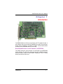
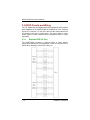
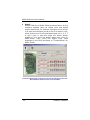
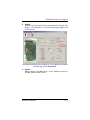
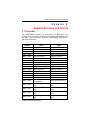
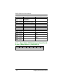
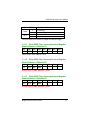
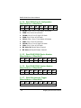
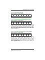
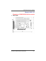
DASP-52096 High-Density 96 Channel DI/O Card User’s Manual Disclaimers The information in this manual has been carefully checked and is believed to be accurate. Axiomtek Co., Ltd. assumes no responsibility for any infringements of patents or other rights of third parties which may result from its use. Axiomtek assumes no responsibility for any inaccuracies that may be contained in this document. Axiomtek makes no commitment to update or to keep current the information contained in this manual. Axiomtek reserves the right to make improvements to this document and/or product at any time and without notice. No part of this document may be reproduced, stored in a retrieval system, or transmitted, in any form or by any means, electronic, mechanical, photocopying, recording, or otherwise, without the prior written permission of Axiomtek Co., Ltd. Copyright 2004 by Axiomtek Co., Ltd. All rights reserved. December 2004, Version A1 Printed in Taiwan ii ESD Precautions Integrated circuits on computer boards are sensitive to static electricity. To avoid damaging chips from electrostatic discharge, observe the following precautions: Do not remove boards or integrated circuits from their anti-static packaging until you are ready to install them. Before handling a board or integrated circuit, touch an unpainted portion of the system unit chassis for a few seconds. This helps to discharge any static electricity on your body. Wear a wrist-grounding strap, available from most electronic component stores, when handling boards and components. Trademarks Acknowledgments AXIOMTEK is a trademark of Axiomtek Co., Ltd. IBM is a registered trademark of International Business Machines Corporation. MS-DOS, and Windows 95/98/NT/2000 are trademarks of Microsoft Corporation. Phoenix-Award is a trademark of Phoenix-Award Software, Inc. IBM, PC/AT, PS/2, VGA are trademarks of International Business Machines Corporation. Intel and Celeron, Pentium III are trademarks of Intel Corporation. Other brand names and trademarks are the properties and registered brands of their respective owners. iii Table of Contents Chapter 1 1.1 1.2 1.3 Chapter 2 2.1 2.2 Introduction................................................. 1 Features ............................................................... 2 Specifications...................................................... 3 Accessories ......................................................... 4 Hardware Installation ............................... 5 Board Layout ....................................................... 5 Signal Connections............................................. 6 2.2.1 Signal Connection Descriptions .......................... 6 2.2.2 Digital Input / Output Connector CON1 .............. 7 2.3 DI/DO Circuits and Wiring ................................ 10 2.3.1 2.3.2 2.3.3 2.3.4 2.4 Emulate 8255 I/O Port .................................... 10 Interrupt Function ......................................... 12 Digital Input Port Circuits and Wiring ............... 13 Digital Output Port Circuits and Wiring ............. 14 Jumper Settings ................................................ 15 2.4.1 JP1: Ch.0/1/2/3 Port Operation Mode Setting ...... 15 2.4.2 JP2: Device Reset Type Selection....................... 16 2.5 Quick Setup and Test ....................................... 17 Chapter 3 3.1 Registry Structure and Format............... 25 Overview ............................................................ 25 3.1.1 Read / Write 8255 Chip0 Input / Output Port A, B and C (Base Address + Offset 0x00-02)........................ 26 3.1.2 Write 8255 Chip 0 Control Word (Base Address + Offset 0x03) ........................................................... 27 3.1.3 Read / Write 8255 Chip1 Input / Output Port A, B and C (Base Address + Offset 0x04-06)........................ 27 3.1.4 Write 8255 Chip 1 Control Word (Base Address + Offset 0x07) ........................................................... 27 3.1.5 Read/Write 8255 Chip2 Input/Output Port A, B and C (Base Address + Offset 0x08-0A)............................. 28 3.1.6 Write 8255 Chip 2 Control Word (Base Address + Offset 0x0B) ........................................................... 28 iv 3.1.7 Read / Write 8255 Chip3 Input / Output Port A, B and C (Base Address + Offset 0x0C-0E) ...................... 28 3.1.8 Read 8255 Chip 2/3 Configuration (Base Address + Offset 0x0F) ........................................................... 29 3.1.9 Write 8255 Chip 3 Control Word (Base Address + Offset 0x0F) ........................................................... 29 3.1.10 Write 8255 Chip 0 Interrupt Control Register (Base Address + Offset 0x10) ............................................ 30 3.1.11 Write 8255 Chip 1 Interrupt Control Register (Base Address + Offset 0x11) ............................................ 31 3.1.12 Write 8255 Chip 2 Interrupt Control Register (Base Address + Offset 0x12) ............................................ 31 3.1.13 Write 8255 Chip 3 Interrupt Control Register (Base Address + Offset 0x13) ............................................ 31 3.1.14 Read 8255 Chip 0/1 Configuration (Base Address + Offset 0x14) ........................................................... 32 3.1.15 Read DASP-52096 Device Number (Base Address + Offset 0x15) ........................................................... 32 3.1.16 Read DASP-52096 Version Number (Base Address + Offset 0x16) ........................................................... 32 3.1.17 Write Soft Interrupt Trigger (Base Address + Offset 0x18) ........................................................... 32 3.1.18 Write Clear Interrupt (Base Address + Offset 0x1A) .............................................................. 33 3.1.19 Write Ch.0 Port A Pattern Match Value (Base Address + Offset 0x1C)............................................ 33 3.1.20 Write Ch.0 Port B Change-of-state Enable (Base Address + Offset 0x1E)............................................ 33 Appendix A Dimension of DASP-52096 and Accessories ...................................................................... 35 v This page does not contain any information. vi DASP-52096 Card User’s Manual Chapter 1 Introduction The DASP-52096 is a PCI-bus, high-density, 96 TTL digital I/O card. It has a higher output current driving capability than 8255, and each port allows users to configure it as inputs or outputs. It also features serial numbers on the EEPROM and PCI scan utility. Board Identification- Serial Number on EEPROM The DASP stores the serial number of each DASP in the EEPROM before shipping. The PCI scan utility can scan all the DASP and show users the serial number of each DASP, helping the user to easily identify and access each card. Introduction 1 DASP-52096 Card User’s Manual 1.1 Features 96 TTL digital I/O channels Buffered circuits for higher driving capacity Multiple-source interrupt handling Interrupt output pin for simultaneously triggering external devices with the interrupt Output status read-back Supports dry contact and wet contact Serial number on EEPROM supported Windows 98/NT/2000/XP and Labview 6.0/7.0 driver supported ® Complete sample program- VB, VC, BCB, Delphi 2 Introduction DASP-52096 Card User’s Manual 1.2 Specifications Digital Inputs Type: TTL level Input voltage: High level 2.0V to 5.2V Low level -0.5V to 0.8V Load current: -0.45mA to +70(A) Digital Outputs Type: TTL level Sink Current: 0.4V@+64mA (Logic level 0) Source current: 2.4@-15mA (Logic level 1) General Environment I/O connector: 100-pin SCSI-II pin type female Power consumption: +5V @ 900mA (max.) Operating temperature: 0 ~ 60°C Storage temperature: -20 ~ 70°C Humility: 0 ~ 90% non-condensing Dimensions: 185mm x 122 mm Introduction 3 DASP-52096 Card User’s Manual 1.3 Accessories To make the DASP-52096 functionality complete, we carry a versatility of accessories for different user’s requirements in the following items: Wiring Cable CB-89200-2: 100-pin SCSI-II pin type male with 2m length CB-89200-5: 100-pin SCSI-II pin type male with 5m length Terminal Block TB-88200: 100-pin SCSI-II terminal block with DIN-rail mounting The terminal block is directly connected to I/O connector CON1 of the DASP-52096. 4 Introduction DASP-52096 Card User’s Manual Chapter 2 Hardware Installation 2.1 Board Layout Board Layout for DASP-52096 Hardware Installation 5 DASP-52096 Card User’s Manual 2.2 Signal Connections 2.2.1 Signal Connection Descriptions Signal Connections for DASP-52096 Referring to the above figure, the accessories of the DASP-52096 and their installation are depicted in the following figure in 2.2.2 and described as below. CON1: The I/O connector CON1 on the DASP-52096 is a 100-pin SCSI-II pin type connector for digital input/output signals. CON1 enables you to connect to accessories, such as the terminal block TB-88200, with the shielded 100-pin SCSI-II pin type cable CB-89200-2 or CB-89200-5. 6 Hardware Installation DASP-52096 Card User’s Manual 2.2.2 Digital Input / Output Connector CON1 CON1 CB-89200 TB-88200 DIO Signal Connections for DASP-52096 with TB-88200 Hardware Installation 7 DASP-52096 Card User’s Manual The pin assignment of CON1 of DASP-52096 is listed as follows. 8 Description Pin Pin Description Ch.0 PA 0 Ch.0 PA 1 Ch.0 PA 2 Ch.0 PA 3 Ch.0 PA 4 Ch.0 PA 5 Ch.0 PA 6 Ch.0 PA 7 Ch.0 PB 0 Ch.0 PB 1 Ch.0 PB 2 Ch.0 PB 3 Ch.0 PB 4 Ch.0 PB 5 Ch.0 PB 6 Ch.0 PB 7 Ch.0 PC 0 Ch.0 PC 1 Ch.0 PC 2 Ch.0 PC 3 Ch.0 PC 4 Ch.0 PC 5 Ch.0 PC 6 Ch.0 PC 7 GND 1 2 3 4 5 6 7 8 9 10 11 12 13 14 15 16 17 18 19 20 21 22 23 24 25 51 52 53 54 55 56 57 58 59 60 61 62 63 64 65 66 67 68 69 70 71 72 73 74 75 Ch.2 PA 0 Ch.2 PA 1 Ch.2 PA 2 Ch.2 PA 3 Ch.2 PA 4 Ch.2 PA 5 Ch.2 PA 6 Ch.2 PA 7 Ch.2 PB 0 Ch.2 PB 1 Ch.2 PB 2 Ch.2 PB 3 Ch.2 PB 4 Ch.2 PB 5 Ch.2 PB 6 Ch.2 PB 7 Ch.2 PC 0 Ch.2 PC 1 Ch.2 PC 2 Ch.2 PC 3 Ch.2 PC 4 Ch.2 PC 5 Ch.2 PC 6 Ch.2 PC 7 GND Hardware Installation DASP-52096 Card User’s Manual Description Pin Pin Description Ch.1 PA 0 Ch.1 PA 1 Ch.1 PA 2 Ch.1 PA 3 Ch.1 PA 4 Ch.1 PA 5 Ch.1 PA 6 Ch.1 PA 7 Ch.1 PA 0 Ch.1 PB 1 Ch.1 PB 2 Ch.1 PB 3 Ch.1 PB 4 Ch.1 PB 5 Ch.1 PB 6 Ch.1 PB 7 Ch.1 PB 0 Ch.1 PC 1 Ch.1 PC 2 Ch.1 PC 3 Ch.1 PC 4 Ch.1 PC 5 Ch.1 PC 6 Ch.1 PC 7 +5V 26 27 28 29 30 31 32 33 34 35 36 37 38 39 40 41 42 43 44 45 46 47 48 49 50 76 77 78 79 80 81 82 83 84 85 86 87 88 89 90 91 92 93 94 95 96 97 98 99 100 Ch.3 PC 0 Ch.3 PA 1 Ch.3 PA 2 Ch.3 PA 3 Ch.3 PA 4 Ch.3 PA 5 Ch.3 PA 6 Ch.3 PA 7 Ch.3 PA 0 Ch.3 PB 1 Ch.3 PB 2 Ch.3 PB 3 Ch.3 PB 4 Ch.3 PB 5 Ch.3 PB 6 Ch.3 PB 7 Ch.3 PB 0 Ch.3 PC 1 Ch.3 PC 2 Ch.3 PC 3 Ch.3 PC 4 Ch.3 PC 5 Ch.3 PC 6 Ch.3 PC 7 +5V Hardware Installation 9 DASP-52096 Card User’s Manual 2.3 DI/DO Circuits and Wiring The TTL digital input and digital output wiring diagrams and functional block diagrams of the DASP-52096 are depicted as in the following figures in 2.3.2 and 2.3.3. The port A and port B of each channel can be configured as input or output ports. The upper nibble or lower nibble of port C of each channel can be configured as input or output separately. 2.3.1 Emulate 8255 I/O Port The DASP-52096 emulates 4 channels 8255 in mode 0(basic input/output) and has an increased output current of 15mA (source) or 64mA (sink), allowing it to drive LED, relay, etc. 10 Hardware Installation DASP-52096 Card User’s Manual Hardware Installation 11 DASP-52096 Card User’s Manual 2.3.2 Interrupt Function The first line of each nibble of port C of all emulated 8255 chips of DASP-52096 can serve as the external interrupt signal source, and the interrupt logics of these lines can be configured as raising edge triggered or falling edge triggered. A pattern-match interrupt logic circuits connect to port A of chip 0, and a change-of-state interrupt logic circuits build with port B of chip 0 provide another combinational interrupt logics for application. All of these 6 interrupt source can be handled simultaneous by DASP-52096. The interrupt function block diagram is given below. Selection & mode control PC0.0 PC0.4 PC1.0 Selection & mode control PC1.4 PC2.0 PCI Bus PCI Bridge Selection & mode control PC2.4 PC3.0 12 Selection & mode control PC3.4 Pattern-match Logic PA0[0:7] Change-ofstate Logic PB0[0:7] Hardware Installation DASP-52096 Card User’s Manual 2.3.3 Digital Input Port Circuits and Wiring There are up to 96 digital input channels on DASP-52096 board. For digital input application, both dry contact inputs and wet contact inputs are acceptable for the IO interface of DASP-52096. The following figure demonstrates the circuit configuration of digital input port. The basic layout and wiring is presented as below. +5V +5V TTL Device DI+ GND GND GND MCU Block Diagram of Internal Circuits and Wiring of TTL Digital Input for DASP-52096 Hardware Installation 13 DASP-52096 Card User’s Manual 2.3.4 Digital Output Port Circuits and Wiring There are up to 96 digital output channels on DASP-52096 board. The following figure demonstrates the circuit configuration. The basic layout is presented as below. +5V +5V GND DO0 TTL Device GND Block Diagram of Internal Circuits and Wiring of TTL Digital Output for DASP-52096 14 Hardware Installation DASP-52096 Card User’s Manual 2.4 Jumper Settings 2.4.1 JP1: Ch.0/1/2/3 Port Operation Mode Setting The JP 1 is used to configure the operation mode of I/O port of DASP-52096. For each emulated 8255, the port A, port B, high nibble of port C and low nibble of port C can be configured as input port or output port independently. The default configuration of the DASP-52096 is to open all the jumpers of JP1 and set each I/O line to operate as input line. To change the operation mode of a specific port (or specific nibble of port C), short the corresponding jumper of JP1. IMPORTANT: If the corresponding jumper of a specific port (nibble) is shorted, the I/O lines belong to the port (nibble) are forced to operate as digital output lines, otherwise, the operation mode of I/O lines of the specific port (nibble) can be software configurable. Set as input port Set as output port JPC0L Ch.0 PC0~3 JPC2L Ch.2 PC0~3 JPB0 Ch.0 PB0~7 JPB2 Ch.2 PB0~7 JPC0H Ch.0 PC4~7 JPC2H Ch.2 PC4~7 JPA0 Ch.0 PA0~7 JPA2 Ch.2 PA0~7 JPC1L Ch.1 PC0~3 JPC3L Ch.3 PC0~3 JPB1 Ch.1 PB0~7 JPB3 Ch.3 PB0~7 JPC1H Ch.1 PC4~7 JPC3H Ch.3 PC4~7 JPA1 Ch.1 PA0~7 JPA3 Ch.3 PA0~7 Hardware Installation 15 DASP-52096 Card User’s Manual 2.4.2 JP2: Device Reset Type Selection The JP2 jumpers are used to configure device reset mode of the DASP-52096. If the “Hot System Reset Mode” is selected, DASP-52096 will reset all its I/O ports status when a bus reset signal is generated by the host PC and propagate through the PCI bus. On the other hand, if the “Power Reset Mode” is selected, DASP-52096 will reset all its I/O port status only when the host PC power off. The I/O ports status of DASP-52096 will be latched during PCI bus reset signal set when the host PC hot reset. Hot System Reset Power Reset Device Reset (JP2) 16 Hardware Installation DASP-52096 Card User’s Manual 2.5 Quick Setup and Test To install a new DASP-52096 into an IBM PC compatible computer, at first, power-off the PC and open its chassis, then plug the DASP-52096 into a PCI slot of mother-board of the PC. The DASP-52096 is a plug and play device for MS Windows, and the OS will detect your DASP-52096 after you power on the PC. The detail of driver and software installation is described in software manual of DASP-52096. After the hardware and software installation, user can emulate and test DASP-52096 step by step as follows. Step 1 To perform a complete test of DASP-52096, we can route the output channels to the input channels of DASP-52096 directly for read-back, for instance, configure chip 0 port A as output channels and configure chip 0 port B as input channels. And then, by following the DASP-52096 test branch of the ToolWorkShop which will fully test all the digital I/O channels of the DASP-52096 as descried in the following paragraphs. Step 2 Launch the ‘PCI Configuration Utility’ of DASP-52000 series to ensure that the resource of DASP-52096 is properly dispatched by the OS. Press the scan button in the toolbar of the ‘PCI Configuration Utility’ to find the installed DASP-52096, and then check the resource list as show in following figure. Hardware Installation 17 DASP-52096 Card User’s Manual Scan DASP-52096 with PCI Configuration Utility and Check the Dispatched Resource 18 Hardware Installation DASP-52096 Card User’s Manual Step 3 Exit the ‘PCI Configuration Utility’ and launch the ‘ToolWorkShop’ for DASP-52096. As shown in the following. Launch ToolWorkShop Select Board Test Hardware Installation 19 DASP-52096 Card User’s Manual Select Test Target: DASP52096 20 Hardware Installation DASP-52096 Card User’s Manual Step 4 Perform DIO test of DASP-52096 as shown in following. At first, check the device information and press ‘Setup’ button to load DASP-52096 library shown below Check Device Information and Press ‘Setup’ Button to Load DASP-52096 Library Hardware Installation 21 DASP-52096 Card User’s Manual Step 5 Perform DIO test of DASP-52096 as shown below. At first, configure selected ports as digital input and digital output respectively, for instance, configure port A of chip 0 as input and configure port B of chip 0 as output. Then, writes 0xAA to turn on all the digital output line 1, 3, 5, 7 of chip 0 port A, and then press the ‘Action’ button related to it to send the digital output port value to DASP-52096. Then, verify the digital input value presented in the DI/O test panel of ‘TOOLWORKSHOP’ for DASP-52096. Perform Digital Input / Output Test by Set the DO Port Value and Read Back the DI Port Value of DASP-52096 22 Hardware Installation DASP-52096 Card User’s Manual Step 6 Perform the Interrupt Test by selecting the Interrupt Test Page in ‘TOOLWORKSHOP’. The Interrupt testing page is as shown below. Select the Interrupt Source and Press Start / Stop Button to Perform the Interrupt Test of DASP-52096 Step 7 Before exiting ‘ToolWorkShop’, press ‘Release’ button to release DASP-52096 library. Hardware Installation 23 DASP-52096 Card User’s Manual This page does not contain any information. 24 Hardware Installation DASP-52096 Card User’s Manual Chapter 3 Register Structure and Format 3.1 Overview The DASP-52096 occupies 32 consecutive I/O addresses. The address of each register is defined as the board’s base address plus an offset. The I/O registers and their corresponding functions are listed in the followings. Address Base + 0x00 Base + 0x01 Base + 0x02 Base + 0x03 Base + 0x04 Base + 0x05 Base + 0x06 Base + 0x07 Base + 0x08 Base + 0x09 Base + 0x0A Base + 0x0B Base + 0x0C Base + 0x0D Base + 0x0E Base + 0x0F Base + 0x10 Base + 0x11 Base + 0x12 Base + 0x13 Read 8255 Ch.0 port A 8255 Ch.0 port B 8255 Ch.0 port C 8255 Ch.1 port A 8255 Ch.1 port B 8255 Ch.1 port C 8255 Ch.2 port A 8255 Ch.2 port B 8255 Ch.2 port C 8255 Ch.3 port A 8255 Ch.3 port B 8255 Ch.3 port C Ch.2 & Ch.3 Configuration Ch.0 Interrupt Control Reg. Ch.1 Interrupt Control Reg. Ch.2 Interrupt Control Reg. Ch.3 Interrupt Control Reg. Registry Structure and Format Write 8255 Ch.0 port A 8255 Ch.0 port B 8255 Ch.0 port C 8255 Ch.0 control word 8255 Ch.1 port A 8255 Ch.1 port B 8255 Ch.1 port C 8255 Ch.1 control word 8255 Ch.2 port A 8255 Ch.2 port B 8255 Ch.2 port C 8255 Ch.2 control word 8255 Ch.2 port A 8255 Ch.2 port B 8255 Ch.2 port C 8255 ch3 control word Ch.0 Interrupt Control Reg. Ch.1 Interrupt Control Reg. Ch.2 Interrupt Control Reg. Ch.3 Interrupt Control Reg. 25 DASP-52096 Card User’s Manual Address Base + 0x14 Base + 0x15 Base + 0x16 Base + 0x17 Base + 0x18 Base + 0x19 Base + 0x1A Base + 0x1B Read Write Ch.0 & Ch.1 Configuration Device Number (0x8f) Version Number (0x01) Software interrupt trigger Clear interrupt Pattern-matching Value Reg. Base + 0x1C Base + 0x1D Change-of-state Enable Reg. Base + 0x1E Base + 0x1F 3.1.1 Read / Write 8255 Chip0 Input / Output Port A, B and C (Base Address + Offset 0x00-02) D7 D6 D5 D4 D3 D2 D1 D0 8 bit Input/Output Data 26 Registry Structure and Format DASP-52096 Card User’s Manual 3.1.2 Write 8255 Chip 0 Control Word (Base Address + Offset 0x03) D7 D6 D5 D4 D3 D2 D1 D0 1 0 0 CA CCU 0 CB CCL CA: Port A input/output control 1: Input, 2: Output CCU: Port C upper 4 bits input/output control 1: Input, 2: Output CB: Port B input/output control 1: Input, 2: Output CCL: Port C lower 4 bits input/output control 1: Input, 2: Output IMPORTANT: The input/output control of specific port (nibble) is effective only when the corresponding jumper of JP1 is opened. (Reference to 2.3.5) 3.1.3 Read / Write 8255 Chip1 Input / Output Port A, B and C (Base Address + Offset 0x04-06) D7 D6 D5 D4 D3 D2 D1 D0 8 bit Input/Output Data Please refer to base address + 0x0 – 0x02 3.1.4 Write 8255 Chip 1 Control Word (Base Address + Offset 0x07) D7 D6 D5 D4 D3 D2 D1 D0 1 0 0 CA CCU 0 CB CCL Please refer to base address + 0x03 Registry Structure and Format 27 DASP-52096 Card User’s Manual 3.1.5 Read/Write 8255 Chip2 Input/Output Port A, B and C (Base Address + Offset 0x08-0A) D7 D6 D5 D4 D3 D2 D1 D0 8 bit Input/Output Data Please refer to base address + 0x0 – 0x02 3.1.6 Write 8255 Chip 2 Control Word (Base Address + Offset 0x0B) D7 D6 D5 D4 D3 D2 D1 D0 1 0 0 CA CCU 0 CB CCL Please refer to base address + 0x03 3.1.7 Read / Write 8255 Chip3 Input / Output Port A, B and C (Base Address + Offset 0x0C-0E) D7 D6 D5 D4 D3 D2 D1 D0 8 bit Input/Output Data Please refer to base address + 0x0 – 0x02 28 Registry Structure and Format DASP-52096 Card User’s Manual 3.1.8 Read 8255 Chip 2/3 Configuration (Base Address + Offset 0x0F) D7 D6 D5 D4 D3 D2 D1 D0 JPC2L JPB2 JPC2H JPA2 JPC3L JPB3 JPC3H JPA3 JPC2L: Chip 2 Port C Low Nibble I/O Mode JPB2: Chip 2 Port B I/O Mode JPC2H: Chip 2 Port C High I/O Mode JPA2: Chip 2 Port A I/O Mode JPC2L: Chip 3 Port C Low Nibble I/O Mode JPB2: Chip 3 Port B I/O Mode JPC2H: Chip 3 Port C High I/O Mode JPA2: Chip 3 Port A I/O Mode Bit Value 0: Digital Input Channel Bit Value 1: Digital Output Channel 3.1.9 Write 8255 Chip 3 Control Word (Base Address + Offset 0x0F) D7 D6 D5 D4 D3 D2 D1 D0 1 0 0 CA CCU 0 CB CCL Please refer to base address + 0x03 Registry Structure and Format 29 DASP-52096 Card User’s Manual 3.1.10 Write 8255 Chip 0 Interrupt Control Register (Base Address + Offset 0x10) D7 D6 D5 D4 D3 D2 D1 D0 IF0 TE0 M01 M00 CSIF CSE PMIF PME Mn0, Mn1: Mode Bit of Chip n, Port C, n = 0, …, 3 PME: Pattern-match Enable Control Bit of Chip 0 Port A CSE: Change-of-state Enable Control Bit of Chip 0 Port B TEn: Trigger Edge Control Bit, n = 0, …, 3 IFn: Interrupt Flag Bit of Chip n, Port C, n = 0, …, 3 PMIF: Pattern-match Interrupt Flag Bit of Chip 0 Port A CSIF: Change-of-state Interrupt Flag Bit of Chip 0 Port B Mn0 Mn1 0 0 1 1 0 1 0 1 PME 0 1 Description Disable Interrupt Interrupt Source Interrupt Source Disable Interrupt PCn.0 PCn.0 & PCn.4 Description Disable Pattern-match Interrupt Enable Pattern-match Interrupt CSE 0 1 TEn 0 1 30 Description Disable Change-of-state Interrupt Enable Change-of-state Interrupt Description Falling Edge Trigger Raising edge Trigger Registry Structure and Format DASP-52096 Card User’s Manual IFn/ PMIF/ CSIF 0 1 0 1 Read Write Description No Interrupt Interrupt Triggered Don’t Care Clear Interrupt* This bit must be set in the ISR to enable next interrupt trigger. 3.1.11 Write 8255 Chip 1 Interrupt Control Register (Base Address + Offset 0x11) D7 D6 D5 D4 D3 D2 D1 D0 IF1 TE1 M11 M10 - - - - Please refer to base address + 0x10 3.1.12 Write 8255 Chip 2 Interrupt Control Register (Base Address + Offset 0x12) D7 D6 D5 D4 D3 D2 D1 D0 IF2 TE2 M21 M20 - - - - Please refer to base address + 0x10 3.1.13 Write 8255 Chip 3 Interrupt Control Register (Base Address + Offset 0x13) D7 D6 D5 D4 D3 D2 D1 D0 IF3 TE3 M31 M30 - - - - Please refer to base address + 0x10 Registry Structure and Format 31 DASP-52096 Card User’s Manual 3.1.14 Read 8255 Chip 0/1 Configuration (Base Address + Offset 0x14) D7 D6 D5 D4 D3 D2 D1 D0 JPC0L JPB0 JPC0H JPA0 JPC1L JPB1 JPC1H JPA1 JPC0L: Chip 0 Port C Low Nibble I/O Mode JPB0: Chip 0 Port B I/O Mode JPC0H: Chip 0 Port C High I/O Mode JPA0: Chip 0 Port A I/O Mode JPC1L: Chip 1 Port C Low Nibble I/O Mode JPB1: Chip 1 Port B I/O Mode JPC1H: Chip 1 Port C High I/O Mode JPA1: Chip 1 Port A I/O Mode Bit Value 0: Digital Input Channel Bit Value 1: Digital Output Channel 3.1.15 Read DASP-52096 Device Number (Base Address + Offset 0x15) D7 D6 D5 D4 D3 D2 D1 D0 1 0 0 0 1 1 1 1 3.1.16 Read DASP-52096 Version Number (Base Address + Offset 0x16) D7 D6 D5 D4 D3 D2 D1 D0 0 0 0 0 0 0 0 1 D1 D0 3.1.17 Write Soft Interrupt Trigger (Base Address + Offset 0x18) D7 D6 D5 D4 D3 D2 Writ any value to trigger interrupt 32 Registry Structure and Format DASP-52096 Card User’s Manual 3.1.18 Write Clear Interrupt (Base Address + Offset 0x1A) D7 D6 D5 D4 D3 D2 D1 D0 Write any value to clear interrupt 3.1.19 Write Ch.0 Port A Pattern Match Value (Base Address + Offset 0x1C) D7 D6 D5 D4 D3 D2 D1 D0 PA.7 PA.6 PA.5 PA.4 PA.3 PA.2 PA.1 PA.0 The contents of referenced pattern used to bit-wise matching with the chip 0 port A input status when the pattern-match interrupt is enabled is build bit-by-bit within the Pattern-match Value register. The LSB of Pattern-match Value register mapped to bit 0 of ch.0 port A(ch.0 PA.0), and the MSB of Pattern-match Value register mapped to bit 7 of ch.0 port A(ch.0 PA.7). 3.1.20 Write Ch.0 Port B Change-of-state Enable (Base Address + Offset 0x1E) D7 D6 D5 D4 D3 D2 D1 D0 PB.7 PB.6 PB.5 PB.4 PB.3 PB.2 PB.1 PB.0 To enable the change-of-state monitoring of specific input lines of Ch.0 port B for Change-of-state interrupt function, SET the corresponding bits of the Change-of-state Enable register. The LSB of Change-of-state Enable register mapped to bit 0 of ch.0 port B(ch.0 PB.0), and the MSB of Change-of-state Enable register mapped to bit 7 of ch.0 port B(ch.0 PB.7). Registry Structure and Format 33 DASP-52096 Card User’s Manual This page does not contain any information. 34 Registry Structure and Format DASP-52096 Card User’s Manual Appendix A Dimension of DASP-52096 and Accessories DASP-52096 Dimension of DASP-52096 and Accessories 35 DASP-52096 Card User’s Manual TB-88200 36 Dimension of DASP-52096 and Accessories