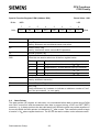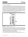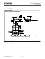
1
C500 ht User’s Manual 01.97 tp :/ Se /ww m w ic .s on ie du me ct ns or .d / e/ Microcontroller Family Architecture and Instruction Set C500 Architecture and Instruction User’s Manual Revision History : 01.97 Original Version Previous Releases: 07.96 Page Subjects (changes since last revision) Table of content 4-89 Reference to pages of each instruction added Table header corrected Edition 01.97 This edition was realized using the software system FrameMaker. Published by Siemens AG, Bereich Halbleiter, MarketingKommunikation, Balanstraße 73, 81541 München © Siemens AG 1997. All Rights Reserved. Attention please! As far as patents or other rights of third parties are concerned, liability is only assumed for components, not for applications, processes and circuits implemented within components or assemblies. The information describes the type of component and shall not be considered as assured characteristics. Terms of delivery and rights to change design reserved. For questions on technology, delivery and prices please contact the Semiconductor Group Offices in Germany or the Siemens Companies and Representatives worldwide (see address list). Due to technical requirements components may contain dangerous substances. For information on the types in question please contact your nearest Siemens Office, Semiconductor Group. Siemens AG is an approved CECC manufacturer. Packing Please use the recycling operators known to you. We can also help you – get in touch with your nearest sales office. By agreement we will take packing material back, if it is sorted. You must bear the costs of transport. For packing material that is returned to us unsorted or which we are not obliged to accept, we shall have to invoice you for any costs incurred. Components used in life-support devices or systems must be expressly authorized for such purpose! Critical components1 of the Semiconductor Group of Siemens AG, may only be used in life-support devices or systems2 with the express written approval of the Semiconductor Group of Siemens AG. 1 A critical component is a component used in a life-support device or system whose failure can reasonably be expected to cause the failure of that life-support device or system, or to affect its safety or effectiveness of that device or system. 2 Life support devices or systems are intended (a) to be implanted in the human body, or (b) to support and/or maintain and sustain human life. If they fail, it is reasonable to assume that the health of the user may be endangered. C500 Table of Contents Page 1 1.1 1.2 1.2.1 1.2.2 1.2.2.1 1.2.2.2 1.2.2.3 1.2.3 Fundamental Structure . . . . . . . . . . . . . . . . . . . . . . . . . . . . . . . . . . . . . . . . . . . . . . Introduction . . . . . . . . . . . . . . . . . . . . . . . . . . . . . . . . . . . . . . . . . . . . . . . . . . . . . . . . . Memory Organization . . . . . . . . . . . . . . . . . . . . . . . . . . . . . . . . . . . . . . . . . . . . . . . . . Program Memory . . . . . . . . . . . . . . . . . . . . . . . . . . . . . . . . . . . . . . . . . . . . . . . . . . . . Data Memory . . . . . . . . . . . . . . . . . . . . . . . . . . . . . . . . . . . . . . . . . . . . . . . . . . . . . . . Internal Data Memory . . . . . . . . . . . . . . . . . . . . . . . . . . . . . . . . . . . . . . . . . . . . . . . . . Internal Data Memory XRAM . . . . . . . . . . . . . . . . . . . . . . . . . . . . . . . . . . . . . . . . . . . External Data Memory . . . . . . . . . . . . . . . . . . . . . . . . . . . . . . . . . . . . . . . . . . . . . . . . Special Function Register Area . . . . . . . . . . . . . . . . . . . . . . . . . . . . . . . . . . . . . . . . . 2 2.1 2.2 2.3 2.4 2.5 2.5.1 2.5.2 2.5.3 2.5.4 2.6 2.7 2.8 CPU Architecture . . . . . . . . . . . . . . . . . . . . . . . . . . . . . . . . . . . . . . . . . . . . . . . . . . . 2-1 Accumulator . . . . . . . . . . . . . . . . . . . . . . . . . . . . . . . . . . . . . . . . . . . . . . . . . . . . . . . . 2-2 B Register . . . . . . . . . . . . . . . . . . . . . . . . . . . . . . . . . . . . . . . . . . . . . . . . . . . . . . . . . . 2-2 Program Status Word . . . . . . . . . . . . . . . . . . . . . . . . . . . . . . . . . . . . . . . . . . . . . . . . . 2-2 Stack Pointer . . . . . . . . . . . . . . . . . . . . . . . . . . . . . . . . . . . . . . . . . . . . . . . . . . . . . . . 2-3 Data Pointer . . . . . . . . . . . . . . . . . . . . . . . . . . . . . . . . . . . . . . . . . . . . . . . . . . . . . . . . 2-4 The Importance of Additional Datapointers . . . . . . . . . . . . . . . . . . . . . . . . . . . . . . . . 2-5 How the eight Datapointers of the C500 are realized . . . . . . . . . . . . . . . . . . . . . . . . . 2-5 Advantages of Multiple Datapointers . . . . . . . . . . . . . . . . . . . . . . . . . . . . . . . . . . . . . 2-6 Application Example and Performance Analysis . . . . . . . . . . . . . . . . . . . . . . . . . . . . 2-6 Enhanced Hooks Emulation Concept . . . . . . . . . . . . . . . . . . . . . . . . . . . . . . . . . . . . . 2-9 Basic Interrupt Handling . . . . . . . . . . . . . . . . . . . . . . . . . . . . . . . . . . . . . . . . . . . . . . 2-10 Interrupt Response Time . . . . . . . . . . . . . . . . . . . . . . . . . . . . . . . . . . . . . . . . . . . . . 2-12 3 3.1 3.2 3.2.1 3.2.2 CPU Timing . . . . . . . . . . . . . . . . . . . . . . . . . . . . . . . . . . . . . . . . . . . . . . . . . . . . . . . . Basic Timing . . . . . . . . . . . . . . . . . . . . . . . . . . . . . . . . . . . . . . . . . . . . . . . . . . . . . . . . Accessing External Memory . . . . . . . . . . . . . . . . . . . . . . . . . . . . . . . . . . . . . . . . . . . . Accessing External Program Memory . . . . . . . . . . . . . . . . . . . . . . . . . . . . . . . . . . . . Accessing External Data Memory . . . . . . . . . . . . . . . . . . . . . . . . . . . . . . . . . . . . . . . 4 4.1 4.2 4.2.1 4.2.2 4.2.3 4.2.4 4.3 Instruction Set . . . . . . . . . . . . . . . . . . . . . . . . . . . . . . . . . . . . . . . . . . . . . . . . . . . . . 4-1 Addressing Modes . . . . . . . . . . . . . . . . . . . . . . . . . . . . . . . . . . . . . . . . . . . . . . . . . . . 4-1 Introduction to the Instruction Set . . . . . . . . . . . . . . . . . . . . . . . . . . . . . . . . . . . . . . . . 4-3 Data Transfer Instructions . . . . . . . . . . . . . . . . . . . . . . . . . . . . . . . . . . . . . . . . . . . . . 4-3 Arithmetic Instructions . . . . . . . . . . . . . . . . . . . . . . . . . . . . . . . . . . . . . . . . . . . . . . . . 4-4 Logic Instructions . . . . . . . . . . . . . . . . . . . . . . . . . . . . . . . . . . . . . . . . . . . . . . . . . . . . 4-5 Control Transfer Instructions . . . . . . . . . . . . . . . . . . . . . . . . . . . . . . . . . . . . . . . . . . . 4-5 Instruction Definitions . . . . . . . . . . . . . . . . . . . . . . . . . . . . . . . . . . . . . . . . . . . . . . . . . 4-7 ACALL addr11 . . . . . . . . . . . . . . . . . . . . . . . . . . . . . . . . . . . . . . . . . . . . . . . . . . . . . 4-9 ADD A, <src-byte> . . . . . . . . . . . . . . . . . . . . . . . . . . . . . . . . . . . . . . . . . . . . . . . 4-10 ADDC A, < src-byte> . . . . . . . . . . . . . . . . . . . . . . . . . . . . . . . . . . . . . . . . . . . . . . 4-12 AJMP addr11 . . . . . . . . . . . . . . . . . . . . . . . . . . . . . . . . . . . . . . . . . . . . . . . . . . . . 4-14 ANL <dest-byte>, <src-byte> . . . . . . . . . . . . . . . . . . . . . . . . . . . . . . . . . . . . . . . 4-15 ANL direct, #data . . . . . . . . . . . . . . . . . . . . . . . . . . . . . . . . . . . . . . . . . . . . . . . . 4-17 ANL C, <src-bit> . . . . . . . . . . . . . . . . . . . . . . . . . . . . . . . . . . . . . . . . . . . . . . . . 4-18 CJNE <dest-byte >, < src-byte >, rel . . . . . . . . . . . . . . . . . . . . . . . . . . . . . . . . . . 4-19 CJNE @Ri, #data, rel . . . . . . . . . . . . . . . . . . . . . . . . . . . . . . . . . . . . . . . . . . . . . 4-21 CLR A . . . . . . . . . . . . . . . . . . . . . . . . . . . . . . . . . . . . . . . . . . . . . . . . . . . . . . . . 4-22 CLR bit . . . . . . . . . . . . . . . . . . . . . . . . . . . . . . . . . . . . . . . . . . . . . . . . . . . . . . . . 4-23 Semiconductor Group I-1 1-1 1-1 1-2 1-2 1-3 1-3 1-5 1-6 1-6 3-1 3-1 3-3 3-3 3-4 C500 Table of Contents 4.4 4.4.1 4.4.2 Page CPL A ........................................................ CPL bit . . . . . . . . . . . . . . . . . . . . . . . . . . . . . . . . . . . . . . . . . . . . . . . . . . . . . . . . DA A ........................................................ DEC byte . . . . . . . . . . . . . . . . . . . . . . . . . . . . . . . . . . . . . . . . . . . . . . . . . . . . . . DIV AB . . . . . . . . . . . . . . . . . . . . . . . . . . . . . . . . . . . . . . . . . . . . . . . . . . . . . . . DJNZ <byte>, <rel-addr> . . . . . . . . . . . . . . . . . . . . . . . . . . . . . . . . . . . . . . . . . . . INC <byte> . . . . . . . . . . . . . . . . . . . . . . . . . . . . . . . . . . . . . . . . . . . . . . . . . . . . INC DPTR . . . . . . . . . . . . . . . . . . . . . . . . . . . . . . . . . . . . . . . . . . . . . . . . . . . . . JB bit,rel . . . . . . . . . . . . . . . . . . . . . . . . . . . . . . . . . . . . . . . . . . . . . . . . . . . . . JBC bit,rel . . . . . . . . . . . . . . . . . . . . . . . . . . . . . . . . . . . . . . . . . . . . . . . . . . . . . JC rel . . . . . . . . . . . . . . . . . . . . . . . . . . . . . . . . . . . . . . . . . . . . . . . . . . . . . . . JMP @A + DPTR . . . . . . . . . . . . . . . . . . . . . . . . . . . . . . . . . . . . . . . . . . . . . . . JNB bit,rel . . . . . . . . . . . . . . . . . . . . . . . . . . . . . . . . . . . . . . . . . . . . . . . . . . . . . JNC rel . . . . . . . . . . . . . . . . . . . . . . . . . . . . . . . . . . . . . . . . . . . . . . . . . . . . . . . JNZ rel . . . . . . . . . . . . . . . . . . . . . . . . . . . . . . . . . . . . . . . . . . . . . . . . . . . . . . . JZ rel . . . . . . . . . . . . . . . . . . . . . . . . . . . . . . . . . . . . . . . . . . . . . . . . . . . . . . . LCALL addr16 . . . . . . . . . . . . . . . . . . . . . . . . . . . . . . . . . . . . . . . . . . . . . . . . . . . . LJMP addr16 . . . . . . . . . . . . . . . . . . . . . . . . . . . . . . . . . . . . . . . . . . . . . . . . . . . . MOV <dest-byte>, <src-byte> . . . . . . . . . . . . . . . . . . . . . . . . . . . . . . . . . . . . . . MOV <dest-bit>, <src-bit> . . . . . . . . . . . . . . . . . . . . . . . . . . . . . . . . . . . . . . . . . MOV DPTR, #data16 . . . . . . . . . . . . . . . . . . . . . . . . . . . . . . . . . . . . . . . . . . . . . MOVC A, @A + <base-reg> . . . . . . . . . . . . . . . . . . . . . . . . . . . . . . . . . . . . . . . . . MOVX <dest-byte>, <src-byte> . . . . . . . . . . . . . . . . . . . . . . . . . . . . . . . . . . . . . . MUL AB . . . . . . . . . . . . . . . . . . . . . . . . . . . . . . . . . . . . . . . . . . . . . . . . . . . . . . . NOP .......................................................... ORL <dest-byte>, <src-byte> . . . . . . . . . . . . . . . . . . . . . . . . . . . . . . . . . . . . . . ORL C, <src-bit> . . . . . . . . . . . . . . . . . . . . . . . . . . . . . . . . . . . . . . . . . . . . . . . . POP direct . . . . . . . . . . . . . . . . . . . . . . . . . . . . . . . . . . . . . . . . . . . . . . . . . . . . . PUSH direct . . . . . . . . . . . . . . . . . . . . . . . . . . . . . . . . . . . . . . . . . . . . . . . . . . . . . RET .......................................................... RETI .......................................................... RL A ........................................................ RLC A ........................................................ RR A ........................................................ RRC A ........................................................ SETB <bit> . . . . . . . . . . . . . . . . . . . . . . . . . . . . . . . . . . . . . . . . . . . . . . . . . . . . . SJMP rel . . . . . . . . . . . . . . . . . . . . . . . . . . . . . . . . . . . . . . . . . . . . . . . . . . . . . . . SUBB A, <src-byte> . . . . . . . . . . . . . . . . . . . . . . . . . . . . . . . . . . . . . . . . . . . . . . . SWAP A . . . . . . . . . . . . . . . . . . . . . . . . . . . . . . . . . . . . . . . . . . . . . . . . . . . . . . . . XCH A, <byte> . . . . . . . . . . . . . . . . . . . . . . . . . . . . . . . . . . . . . . . . . . . . . . . . . . XCHD A,@Ri . . . . . . . . . . . . . . . . . . . . . . . . . . . . . . . . . . . . . . . . . . . . . . . . . . . . XRL <dest-byte>, <src-byte> . . . . . . . . . . . . . . . . . . . . . . . . . . . . . . . . . . . . . . Instruction Set Summary Tables . . . . . . . . . . . . . . . . . . . . . . . . . . . . . . . . . . . . . . . Functional Groups of Instructions . . . . . . . . . . . . . . . . . . . . . . . . . . . . . . . . . . . . . . . Hexadecimal Ordered Instructions . . . . . . . . . . . . . . . . . . . . . . . . . . . . . . . . . . . . . . Semiconductor Group I-2 4-24 4-25 4-26 4-28 4-30 4-31 4-33 4-35 4-36 4-37 4-38 4-39 4-40 4-41 4-42 4-43 4-44 4-45 4-46 4-51 4-52 4-53 4-55 4-57 4-58 4-59 4-62 4-63 4-64 4-65 4-66 4-67 4-68 4-69 4-70 4-71 4-72 4-73 4-75 4-76 4-78 4-79 4-82 4-82 4-87 C500 Table of Contents 5 5.1 5.2 5.3 Page Package Information . . . . . . . . . . . . . . . . . . . . . . . . . . . . . . . . . . . . . . . . . . . . . . . . P-DIP Package . . . . . . . . . . . . . . . . . . . . . . . . . . . . . . . . . . . . . . . . . . . . . . . . . . . . . . PLCC Packages . . . . . . . . . . . . . . . . . . . . . . . . . . . . . . . . . . . . . . . . . . . . . . . . . . . . . MQFP Packages . . . . . . . . . . . . . . . . . . . . . . . . . . . . . . . . . . . . . . . . . . . . . . . . . . . . Semiconductor Group I-3 5-1 5-1 5-2 5-5 Fundamental Structure C500 Family 1 Fundamental Structure 1.1 Introduction The members of the C500 Siemens microcontroller family are basically fully compatible in architecture and software to the standard 8051 microcontroller family. Especially, they are functionally upward compatible to the SAB 80C52/80C32 microcontroller. While maintaining all architectural and operational characteristics of the SAB 80C52/80C32, the C500 microcontrollers differ in number and complexity of their peripheral units which have been adapted to the specific application areas. The goal of this “Architecture and Instruction Set Manual“ is to summarize the basic architecture and functional characteristics of all members of the C500 microcontroller family. This includes the description of the architecture and the description of the complete instruction set. Detailed information about the different versions of the C500 microcontrollers are given in the specific User Manuals. Semiconductor Group 1-1 Fundamental Structure C500 Family 1.2 Memory Organization The memory resources of the C500 family microcontrollers are organized in different types of memories (data and program memory), which further can be located internally on the microcontroller chip or outside of the microcontroller. The memory partitioning of the C500 microcontrollers is typical for a Harvard architecture where data and program areas are held in separate memory areas. The on-chip peripheral units are accessed using an internal special function register memory area. The available memory areas have different sizes and are located in the following five address spaces: Table 1-1 C500 Address Spaces Type of Memory Location Size Program Memory External max. 64 KByte Internal (ROM, EEPROM) Depending on C500 version 2K up to 64KByte External max. 64 KByte Internal XRAM Depending on C500 version 256 Byte up to 3 KByte Internal 128 or 256 Byte Internal 128/256 Bytes Data Memory Special Function Register 1.2.1 Program Memory The program memory of the C500 family microcontrollers can be composed of either completely external program memory, of only internal program memory (on-chip ROM / EEPROM), or of a mixture of internal and external program memory. lf the EA pin (EA=External Access) is held at low level, the C500 microcontrollers execute the program code always out of the external program memory. Romless C500 derivatives can use this type of program memory only. C500 derivatives with on-chip program memory typically use their internal program memory only. If the internal program memory is used the EA pin must be put to high level. With EA high, the microcontroller executes instructions internally unless the address exceeds the upper limit of the internal program memory. If the program counter is set to an address (e.g. by a jump instruction) which is higher than the internal program memory, instructions are executed out of an external program memory. When the instruction address again is below the internal program memory size limit, internal program memory is accessed again. Figure 1-1 shows the typical C500 family microcontroller program memory configuration for the two cases EA=0 and EA=1. The ROM boundary shown in figure 1-1, applies to the C501 which has 8K byte of internal ROM. Other C500 family microcontrollers with different ROM size have different ROM boundaries. Semiconductor Group 1-2 Fundamental Structure C500 Family Figure 1-1 Program Memory Configuration (Example of the C501) 1.2.2 Data Memory The data memory area of the C500 family microcontrollers consists of internal and external data memory portions. The internal data memory area is addressed using 8-bit addresses. The external data memory and the internal XRAM data memory are addressed by 8-bit or16-bit addresses. The content of the internal data memory (also XRAM) is not affected by a reset operation. After power-up the content is undefined, while it remains unchanged during and after a reset as long as the power supply is not turned off. The XRAM content is also maintained when the C500 microcontrollers are in power saving modes. 1.2.2.1 Internal Data Memory The internal data memory address space is divided into three basic, physically separate and distinct blocks: the lower 128 byte of internal data RAM, the upper 128 byte of internal data RAM, and the 128 byte special function register (SFR) area. The lower internal data RAM and the SFR area further include 128 bit locations each. These bits can be handled by specific bit manipulation instructions. Semiconductor Group 1-3 Fundamental Structure C500 Family Figure 1-2 shows the configuration of the three basic internal RAM areas. The lower data RAM is located in the address range 00 H - 7FH and can be addressed directly (e.g. MOV A,direct) or indirectly (e.g. MOV A,@R0 with address in R0). A bit-addressable area of 128 free programmable, direct addressable bits is located at byte addresses 20 H - 2FH of the lower data RAM. Bit 0 of the internal data byte at 20H has the bit address 00H while bit 7 of the internal data byte at 2FH has the bit address 7FH. The lower 32 locations of the internal lower data RAM are assigned to four banks with eight general purpose registers (GPRs) each. Only one of these banks can be enabled at a time to be used as general purpose registers. Figure 1-2 Internal Data Memory Organization Semiconductor Group 1-4 Fundamental Structure C500 Family While the SFR area and the upper internal RAM area share the same address locations (80H FFH), they must be accessed through different addressing modes. The upper internal RAM can only be accessed through indirect addressing while the special function registers (SFRs) are accessible only by direct addressing instructions. The SFRs which are located at addresses with address bit 0-2 equal 0 (addresses 80H, 88H, 90H, ....F0H, FFH) are bitaddressable SFRs. 1.2.2.2 Internal Data Memory XRAM Some members of the C500 family microcontrollers provide an additional internal data memory area, called the XRAM. This data memory area is logically located at the upper end of the external data memory space (except C502), but it is integrated on the chip. Because the XRAM is used in the same way as external data memory the same instruction types must be used for accessing the XRAM. Figure 1-3 shows a typical 256 byte XRAM address mapping of the C500 microcontrollers. Figure 1-3 XRAM Memory Mapping (256 Byte) Depending on the C500 derivative, the size of the XRAM area differs from 128 upto 3K byte. Further, the XRAM can be enabled or disabled. If an internal XRAM area is disabled, external data memory can be accessed in the address range of the internal XRAM. Semiconductor Group 1-5 Fundamental Structure C500 Family 1.2.2.3 External Data Memory The 64 Kbyte external data memory can be addressed by instructions that use 8-bit or 16-bit indirect addressing. A 16-bit external memory addressing mode is supported by the MOVX instructions using the 16-bit datapointer DPTR for addressing. For 8-bit addressing MOVX instructions with the general purpose registers R0/R1 are used. 1.2.3 Special Function Register Area The registers of a C500 microcontroller, except the program counter and the four general purpose register banks, reside in the special function register (SFR) area. The special function register area typically provides 128 bytes of direct addressable SFRs. The SFRs which are located at addresses with address bit 0-2 equal 0 (addresses 80 H, 88H, 90H, ....F0H, FFH) are bitaddressable SFRs (see also figure 1-1). For example, the SFR with byte address 80 H provides the bit locations with bit addresses 80H to 87H. The bit addresses of the SFR bits reach from 80 H to FFH. Due to the limited number of 128 standard SFRs, some derivatives of the C500 microcontroller family provide an additional 128 byte SFR area, called the mapped SFR area. The mapped SFR area provides the same addressing capabilities (direct addresses, bit addressing) as the standard SFR area. Special Function Register SYSCON (Address B1H) Bit No. MSB 7 B1H – 6 5 4 3 2 1 LSB 0 – – RMAP – – – – SYSCON The functions of the shaded bits are not described in this section. Bit Function RMAP Special function register map bit RMAP = 0 : The access to the non-mapped (standard) special function register area is enabled (default after reset). RMAP = 1 : The access to the mapped special function register area is enabled. As long as bit RMAP is set, mapped special function registers can be accessed. This bit is not cleared by hardware automatically. Thus, when non-mapped/mapped registers are to be accessed, the bit RMAP must be cleared/set by software, respectively each. Some registers (e.g. ACC) are accessed independently of bit RMAP. Two bits in the program status word, RS0 (PSW.3) and RS1 (PSW.4), select the active register bank. This allows fast context switching, which is useful when entering subroutines or interrupt service routines. The 8 general purpose registers of the selected register bank may be accessed by register addressing. For indirect addressing modes, the registers R0 and R1 are used as pointer or index register to address internal or external memory (e.g. MOV @R0). Semiconductor Group 1-6 CPU Functions C500 Family 2 CPU Architecture The typical architecture of a C500 family microcontroller is shown in figure 2-1. This block diagram includes all main functional blocks of the C500 microcontrollers. The shaded blocks are basic functional units which are mandatory for each C500 microcontroller. The other functional blocks such as XRAM, peripheral units, and ROM/RAM sizes are specific to each C500 microcontroller derivative. Figure 2-1 C500 Microcontroller Architecture Block Diagram The core block represents the CPU (Central Processing Unit) of the C500 family microcontrollers. The CPU consists of the instruction decoder, the arithmetic section, the CPU registers, and the program control section. The housekeeper unit generates internal signals for controlling the functions of the individual internal units within the microcontroller. Port 0 and port 2 are required for accessing external code and data memory and for emulation purposes. The external control signals and the clock generation are handled in the external control block. The access control unit is responsible for the selection of the on-chip memory resources. The IRAM provides the internal RAM which includes the general purpose registers. The interrupt requests from the peripheral units are handled by an interrupt controller unit. C500 device specific is the configuration of the on-chip peripheral units. Serial interfaces, timers, capture/compare units, A/D converters, watchdog units, or a multiply/divide unit are typical examples for on-chip peripheral units. The external signals of these peripheral units are available at multifunctional parallel I/O ports or at dedicated pins. Semiconductor Group 2-1 CPU Functions C500 Family The arithmetic section of the core performs extensive data manipulation and is comprised of the arithmetic/logic unit (ALU), an A register, B register and PSW register. Further, it has extensive facilities for binary and BCD arithmetic and excels in its bit-handling capabilities. Efficient use of program memory results from an instruction set consisting of 44% one-byte, 41% two-byte, and 15% three-byte instructions. The ALU accepts 8-bit data words from one or two sources and generates an 8-bit result under the control of the instruction decoder. The ALU performs the arithmetic operations add, substract, multiply, divide, increment, decrement, BDC-decimal-addadjust and compare, and the logic operations AND, OR, Exclusive OR, complement and rotate (right, left or swap nibble (left four)). Also included is a Boolean processor performing the bit operations as set, clear, complement, jump-if-not-set, jump-if-set-and-clear and move to/from carry. Between any addressable bit (or its complement) and the carry flag, it can perform the bit operations of logical AND or logical OR with the result returned to the carry flag. The program control section of the core controls the sequence in which the instructions stored in program memory are executed. The 16-bit program counter (PC) holds the address of the next instruction to be executed. The conditional branch logic enables internal and external events to the processor to cause a change in the program execution sequence. 2.1 Accumulator ACC is the symbol for the accumulator register. The mnemonics for accumulator-specific instructions, however, refer to the accumulator simply as A. 2.2 B Register The B register is used during multiply and divide and serves as both source and destination. For other instructions it can be treated as another scratch pad register. 2.3 Program Status Word The Program Status Word (PSW) contains several status bits that reflect the current state of the CPU. The bits of the PSW are used for different functions which are: two register bank selection bits, two carry flags and an overflow flag for arithmetic instructions, a parity bit for the content of the ACC, and two general purpose flags. The bit definitions of the PSW are shown on the next page. Semiconductor Group 2-2 CPU Functions C500 Family Special Function Register PSW (Address D0H) Bit No. D0H Reset Value : 00H MSB LSB 7 6 5 4 3 2 1 0 CY AC F0 RS1 RS0 OV F1 P Bit Function CY Carry Flag Used by arithmetic and conditional branch instruction. AC Auxiliary Carry Flag Used by instructions which execute BCD operations. F0 General Purpose Flag RS1 RS0 Register Bank select control bits These bits are used to select one of the four register banks. PSW RS1 RS0 Function 0 0 Registerbank 0 at data address 00 H-07H selected 0 1 Registerbank 1 at data address 08H-0FH selected 1 0 Registerbank 2 at data address 10H-17H selected 1 1 Registerbank 3 at data address 18H-1FH selected OV Overflow Flag Used by arithmetic instruction. F1 General Purpose Flag P Parity Flag Always set/cleared by hardware to indicate an odd/even number of "one" bits in the accumulator, i.e. even parity. 2.4 Stack Pointer The stack pointer (SP) register is 8 bits wide. It is incremented before data is stored during PUSH and CALL executions and decremented after data is popped during a POP and RET (RETI) execution, i.e. it always points to the last valid stack byte. While the stack may reside anywhere in the on-chip RAM, the stack pointer is initialized to 07H after a reset. This causes the stack to begin a location = 08H above register bank zero. The SP can be read or written under software control. Semiconductor Group 2-3 CPU Functions C500 Family 2.5 Data Pointer 8-bit accesses to the internal XRAM data memory or the external data memory are executed using the data pointer DPTR as an 16-bit address register. Normally, the C500 family microcontrollers have one data pointer. But some members of the C500 family provide eight data pointers. The availability of eight data pointers especially supports the programming in high level languages which have a demand to store data in large external data memory portions. Special Function Register DPL (Address 82H) Special Function Register DPH (Address 83H) Special Function Register DPSEL (Address D0H) Reset Value : 00H Reset Value : 00H Reset Value : 00H MSB LSB Bit No. 7 6 5 4 3 2 1 0 82H .7 .6 .5 .4 .3 .2 .1 LSB DPL 83H MSB .6 .5 .4 .3 .2 .1 .0 DPH 92H – – – – – .2 .1 .0 DPSEL Bit Function – Reserved bits for future use DPSEL.2 - 0 Data pointer select bits DPSEL.2-0 defines the number of the actual active data pointer.DPTR0-7. DPSEL2 DPSEL1 DPSEL0 Function 0 0 0 Data pointer 0 selected 0 0 1 Data pointer 1 selected 0 1 0 Data pointer 2 selected 0 1 1 Data pointer 3 selected 1 0 0 Data pointer 4 selected 1 0 1 Data pointer 5 selected 1 1 0 Data pointer 6 selected 1 1 1 Data pointer 7 selected Semiconductor Group 2-4 CPU Functions C500 Family 2.5.1 The Importance of Additional Datapointers The standard 8051 architecture provides just one 16-bit pointer for indirect addressing of external devices (memories, peripherals, latches, etc.). Except for a 16-bit "move immediate" to this datapointer and an increment instruction, any other pointer handling is to be done byte by byte. For complex applications with peripherals located in the external data memory space (e.g. CAN controller) or extended data storage capacity this turned out to be a "bottle neck" for the 8051’s communication to the external world. Especially programming in high-level languages (PLM51, C51, PASCAL51) requires extended RAM capacity and at the same time a fast access to this additional RAM because of the reduced code efficiency of these languages. 2.5.2 How the eight Datapointers of the C500 are realized Simply adding more datapointers is not suitable because of the need to keep up 100% compatibility to the 8051 instruction set. This instruction set, however, allows the handling of only one single 16bit datapointer (DPTR, consisting of the two 8-bit SFRs DPH and DPL). To meet both of the above requirements (speed up external accesses, 100% compatibility to 8051 architecture) the C500 contains a set of eight 16-bit registers from which the actual datapointer can be selected. This means that the user’s program may keep up to eight 16-bit addresses resident in these registers, but only one register at a time is selected to be the datapointer. Thus the datapointer in turn is accessed (or selected) via indirect addressing. This indirect addressing is done through a special function register called DPSEL (data pointer select register). All instructions of the C500 which handle the datapointer therefore affect only one of the eight pointers which is addressed by DPSEL at that very moment. Figure 5-1 illustrates the addressing mechanism: a 3-bit field in register DPSEL points to the currently used DPTRx. Any standard 8051 instruction (e.g. MOVX @DPTR, A - transfer a byte from accumulator to an external location addressed by DPTR) now uses this activated DPTRx. Semiconductor Group 2-5 CPU Functions C500 Family Figure 2-2 Accessing of External Data Memory via Multiple Datapointers 2.5.3 Advantages of Multiple Datapointers Using the above addressing mechanism for external data memory results in less code and faster execution of external accesses. Whenever the contents of the datapointer must be altered between two or more 16-bit addresses, one single instruction, which selects a new datapointer, does this job. lf the program uses just one datapointer, then it has to save the old value (with two 8-bit instructions) and load the new address, byte by byte. This not only takes more time, it also requires additional space in the internal RAM. 2.5.4 Application Example and Performance Analysis The following example shall demonstrate the involvement of multiple data pointers in a table transfer from the code memory to external data memory. Start address of ROM source table: Start address of table in external RAM: Semiconductor Group 1FFFH 2FA0H 2-6 CPU Functions C500 Family Example 1 : Using only One Datapointer (Code for a C501) Initialization Routine MOV MOV MOV MOV LOW(SRC_PTR), #0FFH HIGH(SRC_PTR), #1FH LOW(DES_PTR), #0A0H HIGH(DES_PTR), #2FH ;Initialize shadow_variables with source_pointer ;Initialize shadow_variables with destination_pointer Table Look-up Routine under Real Time Conditions PUSH PUSH MOV MOV ;INC ;CJNE MOVC MOV MOV MOV MOV INC DPL DPH DPL, LOW(SRC_PTR) DPH, HIGH(SRC_PTR) DPTR … A,@DPTR LOW(SRC_PTR), DPL HIGH(SRC_PTR), DPH DPL, LOW(DES_PTR) DPH, HIGH(DES_PTR) DPTR MOVX MOV MOV POP POP @DPTR, A LOW(DES_PTR), DPL HIGH(DES_PTR),DPH DPH DPL ; Semiconductor Group ; Number of cycles ;Save old datapointer 2 ; 2 ;Load Source Pointer 2 ; 2 Increment and check for end of table (execution time not relevant for this consideration) – ;Fetch source data byte from ROM table 2 ;Save source_pointer and 2 ;load destination_pointer 2 ; 2 ; 2 ;Increment destination_pointer ;(ex. time not relevant) – ;Transfer byte to destination address 2 ;Save destination_pointer 2 ; 2 ;Restore old datapointer 2 ; 2 Total execution time (machine cycles) : 2-7 28 CPU Functions C500 Family Example 2 : Using Two Datapointers (Code for a C509) Initialization Routine MOV MOV MOV MOV DPSEL, #06H DPTR, #1FFFH DPSEL, #07H DPTR, #2FA0H ;Initialize DPTR6 with source pointer ;Initialize DPTR7 with destination pointer Table Look-up Routine under Real Time Conditions PUSH MOV ;INC ;CJNE MOVC MOV DPSEL DPSEL, #06H DPTR … A,@DPTR DPSEL, #07H MOVX POP @DPTR, A DPSEL ; ; Number of cycles ;Save old source pointer 2 ;Load source pointer 2 Increment and check for end of table (execution time not relevant for this consideration) – ;Fetch source data byte from ROM table 2 ;Save source_pointer and ;load destination_pointer 2 ;Transfer byte to destination address 2 ;Save destination pointer and ;restore old datapointer 2 Total execution time (machine cycles) : 12 The above example shows that utilization of the C500’s multiple datapointers can make external bus accesses two times as fast as with a standard 8051 or 8051 derivative. Here, four data variables in the internal RAM and two additional stack bytes were spared, too. This means for some applications where all eight datapointers are employed that an C500 program has up to 24 byte (16 variables and 8 stack bytes) of the internal RAM free for other use. Semiconductor Group 2-8 CPU Functions C500 Family 2.6 Enhanced Hooks Emulation Concept The Enhanced Hooks Emulation Concept of the C500 microcontroller family is a new, innovative way to control the execution of C500 MCUs and to gain extensive information on the internal operation of the controllers. Emulation of on-chip ROM based programs is possible, too. Each production chip has built-in logic for the support of the Enhanced Hooks Emulation Concept. Therefore, no costly bond-out chips are necessary for emulation. This also ensure that emulation and production chips are identical. The Enhanced Hooks TechnologyTM, which requires embedded logic in the C500, allows the C500 together with an EH-IC to function similar to a bond-out chip. This simplifies the design and reduces costs of an ICE-system. ICE-systems using an EH-IC and a compatible C500 are able to emulate all operating modes of the different versions of the C500. This includes emulation of ROM, ROM with code rollover and ROMless modes of operation. It is also able to operate in single step mode and to read the SFRs after a break. ICE-System Interface to Emulation Hardware RESET EA ALE PSEN SYSCON PCON TCON C500 MCU RSYSCON RPCON RTCON EH-IC Enhanced Hooks Interface Circuit Port 0 Port 2 Optional I/O Ports Port 3 Port 1 RPort 2 RPort 0 Target System Interface TEA TALE TPSEN MCS02647 Figure 2-3 Basic C500 MCU Enhanced Hooks Concept Configuration Port 0, port 2 and some of the control lines of the C500 based MCU are used by Enhanced Hooks Emulation Concept to control the operation of the device during emulation and to transfer informations about the program execution and data transfer between the external emulation hardware (ICE-system) and the C500 MCU. Semiconductor Group 2-9 CPU Functions C500 Family 2.7 Basic Interrupt Handling Each member of the C500 microcontroller family provides several interrupt sources. These interrupts are generated typically by external events or by the internal peripheral units. If an interrupt is accepted by the CPU, the microcontroller interrupts a running program and proceeds the program execution at an interrupt source specific vector address where the interrupt service routine is located. After the execution of a RETI (return from interrupt) instruction the program is continued at the point where it has been interrupted. Figure 2-4 shows an example for the interrupt vector addresses of a C500 microcontroller (C501). Generally, interrupt vector addresses are located in the code memory area starting at address 0003 H. The minimum distance between two consecutive vector addresses is always 8 bytes. Therefore, interrupt vectors can be assigned to the following addresses: 0003H, 000BH, 0013H, 001BH, 0023H, 002BH, 0033H ...... 00FBH. Figure 2-4 Interrupt Vector Addresses (Example of the C501) An interrupt source indicates to the interrupt controller an interrupt condition by setting an interrupt request flag. The interrupt request flags are sampled in each machine cycle. The sampled flags are polled during the following machine cycle. If one of the flags was in a set condition in the preceeding cycle, the polling cycle will find it and the interrupt controller will cause the CPU to branch to the vector address of the appropriate service routine by generating an internal LCALL. This hardwaregenerated LCALL is blocked by any of the following conditions: 1. An interrupt of equal or higher priority is already in progress. 2. The current (polling) cycle is not in the final cycle of the instruction in progress. 3. The instruction in progress is RETI or any write access to interrupt enable or priority registers. Semiconductor Group 2-10 CPU Functions C500 Family Any of these three conditions will block the generation of the LCALL to the interrupt service routine. Condition 2 ensures that the instruction in progress is completed before vectoring to any service routine. Condition 3 ensures that if the instruction in progress is RETI or any write access to interrupt enable or interrupt priority registers, then at least one more instruction will be executed before any interrupt is vectored too; this delay guarantees that changes of the interrupt status can be observed by the interrupt controller. The polling cycle is repeated with each machine cycle, and the values polled are the values that were present at the previous machine cycle. Note that if any interrupt flag is active but not being responded to for one of the conditions already mentioned, or if the flag is no longer active when the blocking condition is removed, the denied interrupt will not be serviced. In other words, the fact that the interrupt flag was once active but not serviced is not remembered. Every polling cycle interrogates only the pending interrupt requests. The polling cycle/LCALL sequence is illustrated in figure 2-1. C1 C2 C3 C4 C5 S5P2 Interrupt is latched Interrupts are polled Long Call to Interrupt Vector Address Interrupt Routine MCT01859 Figure 2-5 Interrupt Detection/Entry Diagram Note that if an interrupt of a higher priority level goes active prior to S5P2 in the machine cycle labeled C3 in figure 2-5 then, in accordance with the above rules, it will be vectored to during C5 and C6 without any instruction for the lower priority routine to be executed. Thus, the processor acknowledges an interrupt request by executing a hardware-generated LCALL to the appropriate servicing routine. In some cases it also clears the flag that generated the interrupt, while in other cases it does not; then this has to be done by the user’s software. The program execution proceeds from that location until the RETI instruction is encountered. The RETI instruction informs the processor that the interrupt routine is no longer in progress, then pops the two top bytes from the stack and reloads the program counter. Execution of the interrupted program continues from the point where it was stopped. Note that the RETI instruction is very important because it informs the processor that the program left the current interrupt priority level. A simple RET instruction would also have returned execution to the interrupted program, but it would have left the interrupt control system thinking an interrupt was still in progress. In this case no interrupt of the same or lower priority level would be acknowledged. Semiconductor Group 2-11 CPU Functions C500 Family 2.8 Interrupt Response Time If an external interrupt is recognized, its corresponding request flag is set at S5P2 in every machine cycle. The value is not polled by the circuitry until the next machine cycle. If the request is active and conditions are right for it to be acknowledged, a hardware subroutine call to the requested service routine will be next instruction to be executed. The call itself takes two cycles. Thus a minimum of three complete machine cycles will elapse between activation and external interrupt request and the beginning of execution of the first instruction of the service routine. A longer response time would be obtained if the request was blocked by one of the three previously listed conditions. If an interrupt of equal or higher priority is already in progress, the additional wait time obviously depends on the nature of the other interrupt’s service routine. If the instruction in progress is not in its final cycle, the additional wait time cannot be more than 3 cycles since the longest instructions (MUL and DIV) are only 4 cycles long; and, if the instruction in progress is RETI or a write access to interrupt enable or interrupt priority registers the additional wait time cannot be more than 5 cycles (a maximum of one more cycle to complete the instruction in progress, plus 4 cycles to complete the next instruction, if the instruction is MUL or DIV). Thus a single interrupt system, the response time is always more than 3 cycles and less than 9 cycles. Semiconductor Group 2-12 CPU Timing C500 Family 3 CPU Timing 3.1 Basic Timing A machine cycle consists of 6 states. Each state is divided into a phase 1 half, during which the phase 1 clock is active, and a phase 2 half, during which the phase 2 clock is active. Thus, a machine cycle consists of the states S1P1 (state 1, phase 1) through S6P2 (state 6, phase 2). Depending on the C500 type of microcontroller, each state lasts either one or two periods of the oscillator clock. Typically, arithmetic and logical operations take place during phase 1 and internal register-to-register transfers take place during phase 2. The diagrams in figure 3-1 show the fetch/execute timing related to the internal states and phases. Since these internal clock signals are not user-accessible, the ALE (address latch enable) signal is shown for external reference. ALE is normally activated twice during each machine cycle: once during S1P2 and S2P1, and again during S4P2 and S5P1. The execution of a one-cycle instruction begins at S1P2, when the opcode is latched into the instruction register. If it is a two-byte instruction, the second reading takes place during S4 of the same machine cycle. If it is a one-byte instruction, there is still a fetch at S4, but the byte read (which would be the next op-code) is ignored (discarded fetch), and the program counter is not incremented. In any case, execution is completed at the end of S6P2. Figures 3-1 (a) and (b) show the timing of a 1-byte, 1-cycle instruction and for a 2-byte, 1-cycle instruction. Most C500 instructions are executed in one cycle. MUL (multiply) and DIV (divide) are the only instructions that take more than two cycles to complete; they take four cycles. Normally two code bytes are fetched from the program memory during every machine cycle. The only exception to this is when a MOVX instruction is executed. MOVX is a one-byte, 2-cycle instruction that accesses external data memory. During a MOVX, the two fetches in the second cycle are skipped while the external data memory is being addressed and strobed. Figure 3-1 (c) and (d) show the timing for a normal 1-byte, 2-cycle instruction and for a MOVX instruction. Semiconductor Group 3-1 CPU Timing C500 Family Figure 3-1 Fetch Execute Sequence Semiconductor Group 3-2 CPU Timing C500 Family 3.2 Accessing External Memory There are two types of external memory accesses: accesses to external program memory and accesses to external data memory. Accesses to external program memory use the signal PSEN (program store enable) as the read strobe. Accesses to external data memory use the RD or WR (alternate functions of P3.7 and P3.6) to access the memory. Fetches from external program memory always use a 16-bit address. Accesses to external data memory can use either a 16-bit address (MOVX @DPTR) or an 8-bit address (MOVX @Ri). Whenever a 16-bit address is used, the high byte of the address comes out on port 2, where it is held for the duration of the read, write, or code fetch cycle. If an 8-bit address is being used (MOVX @Ri), the contents of the port 2 SFR remain at the port 2 pins throughout the whole external memory cycle. In this case, port 2 pins can be used to page the external data memory. In either case, the low byte of the address is time-multiplexed with the data byte on port 0. The ADDRESS/DATA signal drives both FETS in the port 0 output buffers. Thus, in external bus mode the port 0 pins are not open-drain outputs and do not require external pullups. The ALE (address latch enable) signal should be used to latch the address byte into an external latch. The address byte is valid at the negative transition of ALE. Then, in a write cycle, the data byte to be written appears on port 0 just before WR is activated, and remains there until WR is deactivated. In a read cycle, the incoming byte is accepted at port 0 just before the read strobe (RD) is deactivated. During any access to external memory, the CPU writes FFH to the port 0 latch (the special function register), thus obliterating the information in the port 0 SFR. Also, a MOV P0 instruction must not take place during external memory accesses. If the user writes to port 0 during an external memory fetch, the incoming code byte may be corrupted. Therefore, do not write to port 0 if external memory is used. 3.2.1 Accessing External Program Memory External program memory is accessed under two conditions: 1. Whenever signal EA is active (low), or 2. Whenever signal EA is inactive (high) and the program counter (PC) contains an address greater than the internal ROM size (e.g. 1FFFFH for an 8K internal ROM or 3FFFH for an 16K internal ROM). This requires that the ROMless versions have always EA wired to Vss to enable the lower 8K, 16K, or 32K program bytes to be fetched from external memory. When the CPU is executing out from external program memory (see timing diagram in figure 3-2), all 8 bits of port 2 are dedicated to an output function and may not be used for general purpose I/O. During external program fetches they output the high byte of the PC with the port 2 drivers using the strong pullups to emit bits that are 1´s. Semiconductor Group 3-3 CPU Timing C500 Family Figure 3-2 External Program Memory Fetches 3.2.2 Accessing External Data Memory The port 2 drivers use the strong pullups during the entire time that they are emitting address bits that are 1´s. This occurs when the MOVX @DPTR instruction is executed and when external program fetches are executed. During this time the port 2 latch (the special function register) does not have to contain 1´s, and the contents of the port 2 SFR are not modified. If the external memory cycle is not immediately followed by another external memory cycle, the undisturbed contents of the port 2 SFR will reappear in the next cycle. Figure 3-3 and 3-4 show in detail the timings of the external data memory read and write cycles. Semiconductor Group 3-4 CPU Timing C500 Family Figure 3-3 External Data Memory Read Cycle Figure 3-4 External Data Memory Write Cycle Semiconductor Group 3-5 Instruction Set C500 Family 4 Instruction Set The C500 8-bit microcontroller family instruction set includes 111 instructions, 49 of which are single-byte, 45 two-byte and 17 three-byte instructions. The instruction opcode format consists of a function mnemonic followed by a ”destination, source” operand field. This field specifies the data type and addressing method(s) to be used. Like all other members of the 8051-family, the C500 microcontrollers can be programmed with the same instruction set common to the basic member, the SAB 8051. Thus, the C500 family microcontrollers are 100% software compatible to the SAB 8051 and may be programmed with 8051 assembler or high-level languages. 4.1 Addressing Modes The C500 uses five addressing modes: – – – – – register direct immediate register indirect base register plus index-register indirect Table 4-1 summarizes the memory spaces which may be accessed by each of the addressing modes. Register Addressing Register addressing accesses the eight working registers (R0 - R7) of the selected register bank. The least significant bit of the instruction opcode indicates which register is to be used. ACC, B, DPTR and CY, the Boolean processor accumulator, can also be addressed as registers. Direct Addressing Direct addressing is the only method of accessing the special function registers. The lower 128 bytes of internal RAM are also directly addressable. Immediate Addressing Immediate addressing allows constants to be part of the instruction in program memory. Semiconductor Group 4-1 Instruction Set C500 Family Table 4-1 Addressing Modes and Associated Memory Spaces Addressing Modes Associated Memory Spaces Register addressing R0 through R7 of selected register bank, ACC, B, CY (Bit), DPTR Direct addressing Lower 128 bytes of internal RAM, special function registers Immediate addressing Program memory Register indirect addressing Internal RAM (@R1, @R0, SP), external data memory (@R1, @R0, @DPTR) Base register plus index register addressing Program memory (@A + DPTR, @A + PC) Register Indirect Addressing Register indirect addressing uses the contents of either R0 or R1 (in the selected register bank) as a pointer to locations in a 256-byte block: the 256 bytes of internal RAM or the lower 256 bytes of external data memory. Note that the special function registers are not accessible by this method. The upper half of the internal RAM can be accessed by indirect addressing only. Access to the full 64 Kbytes of external data memory address space is accomplished by using the 16-bit data pointer. Execution of PUSH and POP instructions also uses register indirect addressing. The stack may reside anywhere in the internal RAM. Base Register plus Index Register Addressing Base register plus index register addressing allows a byte to be accessed from program memory via an indirect move from the location whose address is the sum of a base register (DPTR or PC) and index register, ACC. This mode facilitates look-up table accesses. Boolean Processor The Boolean processor is a bit processor integrated into the C500 family microcontrollers. It has its own instruction set, accumulator (the carry flag), bit-addressable RAM and l/O. The bit manipulation instructions allow: – – – – – – – set bit clear bit complement bit jump if bit is set jump if bit is not set jump if bit is set and clear bit move bit from / to carry Addressable bits, or their complements, may be logically AND-ed or OR-ed with the contents of the carry flag. The result is returned to the carry register. Semiconductor Group 4-2 Instruction Set C500 Family 4.2 Introduction to the Instruction Set The instruction set is divided into four functional groups: – – – – 4.2.1 data transfer arithmetic logic control transfer Data Transfer Instructions Data transfer operations are divided into three classes: – general-purpose – accumulator-specific – address-object None of these operations affects the PSW flag settings except a POP or MOV directly to the PSW. General-Purpose Transfers – MOV performs a bit or byte transfer from the source operand to the destination operand. – PUSH increments the SP register and then transfers a byte from the source operand to the stack location currently addressed by SP. – POP transfers a byte operand from the stack location addressed by the SP to the destination operand and then decrements SP. Accumulator-Specific Transfers – XCH exchanges the byte source operand with register A (accumulator). – XCHD exchanges the low-order nibble of the source operand byte with the low-order nibble of A. – MOVX performs a byte move between the external data memory and the accumulator. The external address can be specified by the DPTR register (16 bit) or the R1 or R0 register (8 bit). – MOVC moves a byte from program memory to the accumulator. The operand in A is used as an index into a 256-byte table pointed to by the base register (DPTR or PC). The byte operand accessed is transferred to the accumulator. Address-Object Transfer – MOV DPTR, #data loads 16 bits of immediate data into a pair of destination registers, DPH and DPL. Semiconductor Group 4-3 Instruction Set C500 Family 4.2.2 Arithmetic Instructions The C500 family microcontrollers have four basic mathematical operations. Only 8-bit operations using unsigned arithmetic are supported directly. The overflow flag, however, permits the addition and subtraction operation to serve for both unsigned and signed binary integers. Arithmetic can also be performed directly on packed BCD representations. Addition – INC (increment) adds one to the source operand and puts the result in the operand (flags in PSW are not affected). – ADD adds A to the source operand and returns the result to A. – ADDC (add with carry) adds A and the source operand, then adds one (1) if CY is set, and puts the result in A. – DA (decimal-add-adjust for BCD addition) corrects the sum which results from the binary addition of two-digit decimal operands. The packed decimal sum formed by DA is returned to A. CY is set if the BCD result is greater than 99; otherwise, it is cleared. Subtraction – SUBB (subtract with borrow) subtracts the second source operand from the first operand (the accumulator), subtracts one (1) if CY is set and returns the result to A. – DEC (decrement) subtracts one (1) from the source operand and returns the result to the operand (flags in PSW are not affected). Multiplication – MUL performs an unsigned multiplication of the A register by the B register, returning a double byte result. A receives the low-order byte, B receives the high-order byte. OV is cleared if the top half of the result is zero and is set if it is not zero. CY is cleared. AC is unaffected. Division – DIV performs an unsigned division of the A register by the B register; it returns the integer quotient to the A register and returns the fractional remainder to the B register. Division by zero leaves indeterminate data in registers A and B and sets OV; otherwise, OV is cleared. CY is cleared. AC remains unaffected. Flags Unless otherwise stated in the previous descriptions, the flags of PSW are affected as follows: – CY is set if the operation causes a carry to or a borrow from the resulting high-order bit; otherwise CY is cleared. – AC is set if the operation results in a carry from the low-order four bits of the result (during addition), or a borrow from the high-order bits to the low-order bits (during subtraction); otherwise AC is cleared. – OV is set if the operation results in a carry to the high-order bit of the result but not a carry from the bit, or vice versa; otherwise OV is cleared. OV is used in two’s-complement arithmetic, because it is set when the signal result cannot be represented in 8 bits. – P is set if the modulo-2 sum of the eight bits in the accumulator is 1 (odd parity); otherwise P is cleared (even parity). When a value is written to the PSW register, the P bit remains unchanged, as it always reflects the parity of A. Semiconductor Group 4-4 Instruction Set C500 Family 4.2.3 Logic Instructions The C500 family microcontrollers perform basic logic operations on both bit and byte operands. Single-Operand Operations – CLR sets A or any directly addressable bit to zero (0). – SETB sets any directly bit-addressable bit to one (1). – CPL is used to complement the contents of the A register without affecting any flag, or any directly addressable bit location. – RL, RLC, RR, RRC, SWAP are the five operations that can be performed on A. RL, rotate left, RR, rotate right, RLC, rotate left through carry, RRC, rotate right through carry, and SWAP, rotate left four. For RLC and RRC the CY flag becomes equal to the last bit rotated out. SWAP rotates A left four places to exchange bits 3 through 0 with bits 7 through 4. Two-Operand Operations – ANL performs bitwise logical AND of two operands (for both bit and byte operands) and returns the result to the location of the first operand. – ORL performs bitwise logical OR of two source operands (for both bit and byte operands) and returns the result to the location of the first operand. – XRL performs logical Exclusive OR of two source operands (byte operands) and returns the result to the location of the first operand. 4.2.4 Control Transfer Instructions There are three classes of control transfer operations: unconditional calls, returns, jumps, conditional jumps, and interrupts. All control transfer operations, some upon a specific condition, cause the program execution to continue a non-sequential location in program memory. Semiconductor Group 4-5 Instruction Set C500 Family Unconditional Calls, Returns and Jumps Unconditional calls, returns and jumps transfer control from the current value of the program counter to the target address. Both direct and indirect transfers are supported. – ACALL and LCALL push the address of the next instruction onto the stack and then transfer control to the target address. ACALL is a 2-byte instruction used when the target address is in the current 2K page. LCALL is a 3-byte instruction that addresses the full 64K program space. In ACALL, immediate data (i.e. an 11-bit address field) is concatenated to the five most significant bits of the PC (which is pointing to the next instruction). If ACALL is in the last 2 bytes of a 2K page then the call will be made to the next page since the PC will have been incremented to the next instruction prior to execution. – RET transfers control to the return address saved on the stack by a previous call operation and decrements the SP register by two (2) to adjust the SP for the popped address. – AJMP, LJMP and SJMP transfer control to the target operand. The operation of AJMP and LJMP are analogous to ACALL and LCALL. The SJMP (short jump) instruction provides for transfers within a 256-byte range centered about the starting address of the next instruction (– 128 to + 127). – JMP @A + DPTR performs a jump relative to the DPTR register. The operand in A is used as the offset (0 - 255) to the address in the DPTR register. Thus, the effective destination for a jump can be anywhere in the program memory space. Conditional Jumps Conditional jumps perform a jump contingent upon a specific condition. The destination will be within a 256-byte range centered about the starting address of the next instruction (– 128 to + 127). – – – – – – – JZ performs a jump if the accumulator is zero. JNZ performs a jump if the accumulator is not zero. JC performs a jump if the carry flag is set. JNC performs a jump if the carry flag is not set. JB performs a jump if the directly addressed bit is set. JNB performs a jump if the directly addressed bit is not set. JBC performs a jump if the directly addressed bit is set and then clears the directly addressed bit. – CJNE compares the first operand to the second operand and performs a jump if they are not equal. CY is set if the first operand is less than the second operand; otherwise it is cleared. Comparisons can be made between A and directly addressable bytes in internal data memory or an immediate value and either A, a register in the selected register bank, or a register indirectly addressable byte of the internal RAM. – DJNZ decrements the source operand and returns the result to the operand. A jump is performed if the result is not zero. The source operand of the DJNZ instruction may be any directly addressable byte in the internal data memory. Either direct or register addressing may be used to address the source operand. Interrupt Returns – RETI transfers control as RET does, but additionally enables interrupts of the current priority level. Semiconductor Group 4-6 Instruction Set C500 Family 4.3 Instruction Definitions All 111 instructions of the C500 family microcontrollers can essentially be condensed to 53 basic operations, in the following alphabetically ordered according to the operation mnemonic section. Table 4-2 PSW Flag Modification (CY,OV,AC) Instruction Flag Instruction Flag CY OV AC CY ADD X X X SETB C 1 ADDC X X X CLR C 0 SUBB X X X CPL C X MUL 0 X ANL C,bit X DIV 0 X ANL C,/bit X DA X ORL C,bit X RRC X ORL C,/bit X RLC X MOV C,bit X CJNE X OV AC A brief example of how the instruction might be used is given as well as its effect on the PSW flags. The number of bytes and machine cycles required, the binary machine language encoding, and a symbolic description or restatement of the function is also provided. Note: Only the carry, auxiliary carry, and overflow flags are discussed. The parity bit is always computed from the actual content of the accumulator. Similarly, instructions which alter directly addressed registers could affect the other status flags if the instruction is applied to the PSW. Status flags can also be modified by bit manipulation. Semiconductor Group 4-7 Instruction Set C500 Family Notes on Data Addressing Modes: Rn - Working register R0-R7 direct - 128 internal RAM locations, any l/O port, control or status register @Ri - Indirect internal or external RAM location addressed by register R0 or R1 #data - 8-bit constant included in instruction #data 16 - 16-bit constant included as bytes 2 and 3 of instruction bit - 128 software flags, any bit-addressable l/O pin, control or status bit A - Accumulator Notes on Program Addressing Modes: addr16 - Destination address for LCALL and LJMP may be anywhere within the 64-Kbyte program memory address space. addr11 - Destination address for ACALL and AJMP will be within the same 2-Kbyte page of program memory as the first byte of the following instruction. rel - SJMP and all conditional jumps include an 8-bit offset byte. Range is + 127/– 128 bytes relative to the first byte of the following instruction. All mnemonics copyrighted: Semiconductor Group Intel Corporation 1980 4-8 Instruction Set C500 Family ACALL addr11 Function: Absolute call Description: ACALL unconditionally calls a subroutine located at the indicated address. The instruction increments the PC twice to obtain the address of the following instruction, then pushes the 16-bit result onto the stack (low-order byte first) and increments the stack pointer twice. The destination address is obtained by successively concatenating the five high-order bits of the incremented PC, op code bits 7-5, and the second byte of the instruction. The subroutine called must therefore start within the same 2K block of program memory as the first byte of the instruction following ACALL. No flags are affected. Example: Initially SP equals 07H. The label ”SUBRTN” is at program memory location 0345H. After executing the instruction ACALL SUBRTN at location 0123H, SP will contain 09H, internal RAM location 08H and 09H will contain 25H and 01H, respectively, and the PC will contain 0345H. Operation: ACALL (PC) ← (PC) + 2 (SP) ← (SP) + 1 ((SP)) ← (PC7-0) (SP) ← (SP) + 1 ((SP)) ← (PC15-8) (PC10-0) ← page address Encoding: a10 a9 a8 1 Bytes: 2 Cycles: 2 Semiconductor Group 0 0 0 1 a7 a6 a5 a4 4-9 a3 a2 a1 a0 Instruction Set C500 Family ADD A, <src-byte> Function: Add Description: ADD adds the byte variable indicated to the accumulator, leaving the result in the accumulator. The carry and auxiliary carry flags are set, respectively, if there is a carry out of bit 7 or bit 3, and cleared otherwise. When adding unsigned integers, the carry flag indicates an overflow occurred. OV is set if there is a carry out of bit 6 but not out of bit 7, or a carry out of bit 7 but not out of bit 6; otherwise OV is cleared. When adding signed integers, OV indicates a negative number produced as the sum of two positive operands, or a positive sum from two negative operands. Four source operand addressing modes are allowed: register, direct, registerindirect, or immediate. Example: The accumulator holds 0C3H (11000011B) and register 0 holds 0AAH (10101010B). The instruction ADD A,R0 will leave 6DH (01101101B) in the accumulator with the AC flag cleared and both the carry flag and OV set to 1. ADD Operation: Encoding: A,Rn ADD (A) ← (A) + (Rn) 0 0 1 0 Bytes: 1 Cycles: 1 ADD Operation: Encoding: 1 r r r A,direct ADD (A) ← (A) + (direct) 0 0 1 0 Bytes: 2 Cycles: 1 Semiconductor Group 0 1 0 1 direct address 4-10 Instruction Set C500 Family ADD Operation: Encoding: A, @Ri ADD (A) ← (A) + ((Ri)) 0 0 1 0 Bytes: 1 Cycles: 1 ADD Operation: Encoding: 0 1 1 i A, #data ADD (A) ← (A) + #data 0 0 1 0 Bytes: 2 Cycles: 1 Semiconductor Group 0 1 0 0 immediate data 4-11 Instruction Set C500 Family ADDC A, < src-byte> Function: Add with carry Description: ADDC simultaneously adds the byte variable indicated, the carry flag and the accumulator contents, leaving the result in the accumulator. The carry and auxiliary carry flags are set, respectively, if there is a carry out of bit 7 or bit 3, and cleared otherwise. When adding unsigned integers, the carry flag indicates an overflow occurred. OV is set if there is a carry out of bit 6 but not out of bit 7, or a carry out of bit 7 but not out of bit 6; otherwise OV is cleared. When adding signed integers, OV indicates a negative number produced as the sum of two positive operands or a positive sum from two negative operands. Four source operand addressing modes are allowed: register, direct, registerindirect, or immediate. Example: The accumulator holds 0C3 H (11000011B) and register 0 holds 0AAH (10101010B) with the carry flag set. The instruction ADDC A,R0 will leave 6EH (01101110B) in the accumulator with AC cleared and both the carry flag and OV set to 1. ADDC Operation: Encoding: A,Rn ADDC (A) ← (A) + (C) + (Rn) 0 0 1 1 Bytes: 1 Cycles: 1 ADDC A,direct Operation: Encoding: 1 r r r ADDC (A) ← (A) + (C) + (direct) 0 0 1 1 Bytes: 2 Cycles: 1 Semiconductor Group 0 1 0 1 direct address 4-12 Instruction Set C500 Family ADDC Operation: Encoding: A, @Ri ADDC (A) ← (A) + (C) + ((Ri)) 0 0 1 1 Bytes: 1 Cycles: 1 ADDC A, #data Operation: Encoding: 0 1 1 i ADDC (A) ← (A) + (C) + #data 0 0 1 1 Bytes: 2 Cycles: 1 Semiconductor Group 0 1 0 0 immediate data 4-13 Instruction Set C500 Family AJMP addr11 Function: Absolute jump Description: AJMP transfers program execution to the indicated address, which is formed at runtime by concatenating the high-order five bits of the PC (after incrementing the PC twice), op code bits 7-5, and the second byte of the instruction. The destination must therefore be within the same 2K block of program memory as the first byte of the instruction following AJMP. Example: The label ”JMPADR” is at program memory location 0123H. The instruction AJMP JMPADR is at location 0345H and will load the PC with 0123H. Operation: AJM P (PC) ← (PC) + 2 (PC10-0) ← page address Encoding: a10 a9 a8 0 Bytes: 2 Cycles: 2 Semiconductor Group 0 0 0 1 a7 a6 a5 a4 4-14 a3 a2 a1 a0 Instruction Set C500 Family ANL <dest-byte>, <src-byte> Function: Logical AND for byte variables Description: ANL performs the bitwise logical AND operation between the variables indicated and stores the results in the destination variable. No flags are affected. The two operands allow six addressing mode combinations. When the destination is a accumulator, the source can use register, direct, register-indirect, or immediate addressing; when the destination is a direct address, the source can be the accumulator or immediate data. Note: When this instruction is used to modify an output port, the value used as the original port data will be read from the output data latch, not the input pins. Example: If the accumulator holds 0C3H (11000011B) and register 0 holds 0AAH (10101010B) then the instruction ANL A,R0 will leave 81H (10000001B) in the accumulator. When the destination is a directly addressed byte, this instruction will clear combinations of bits in any RAM location or hardware register. The mask byte determining the pattern of bits to be cleared would either be a constant contained in the instruction or a value computed in the accumulator at run-time. The instruction ANL P1, #01110011B will clear bits 7, 3, and 2 of output port 1. ANL Operation: Encoding: A,Rn ANL (A) ← (A) ∧ (Rn) 0 1 0 1 Bytes: 1 Cycles: 1 ANL Operation: Encoding: 1 r r r A,direct ANL (A) ← (A) ∧ (direct) 0 1 0 1 Bytes: 2 Cycles: 1 Semiconductor Group 0 1 0 1 direct address 4-15 Instruction Set C500 Family ANL Operation: Encoding: A, @Ri ANL (A) ← (A) ∧ ((Ri)) 0 1 0 1 Bytes: 1 Cycles: 1 ANL Operation: Encoding: A, #data ANL (A) ← (A) ∧ #data 0 1 0 1 Bytes: 2 Cycles: 1 ANL Operation: Encoding: 0 1 1 i 0 1 0 0 immediate data direct,A ANL (direct) ← (direct) ∧ (A) 0 1 0 1 Bytes: 2 Cycles: 1 Semiconductor Group 0 1 0 1 direct address 4-16 Instruction Set C500 Family ANL Operation: Encoding: direct, #data ANL (direct) ← (direct) ∧ #data 0 1 0 1 Bytes: 3 Cycles: 2 Semiconductor Group 0 0 1 1 direct address 4-17 immediate data Instruction Set C500 Family ANL C, <src-bit> Function: Logical AND for bit variables Description: If the Boolean value of the source bit is a logic 0 then clear the carry flag; otherwise leave the carry flag in its current state. A slash (”/” preceding the operand in the assembly language indicates that the logical complement of the addressed bit is used as the source value, but the source bit itself is not affected. No other flags are affected. Only direct bit addressing is allowed for the source operand. Example: Set the carry flag if, and only if, P1.0 = 1, ACC.7 = 1, and OV = 0: MOV ANL ANL ANL Operation: Encoding: ANL (C) ← (C) ∧ (bit) 1 0 0 0 2 Cycles: 2 Operation: Encoding: ; Load carry with input pin state ; AND carry with accumulator bit 7 ; AND with inverse of overflow flag C,bit Bytes: ANL C,P1.0 C,ACC.7 C,/OV 0 0 1 0 bit address C,/bit ANL (C) ← (C) ∧ / (bit) 1 0 1 1 Bytes: 2 Cycles: 2 Semiconductor Group 0 0 0 0 bit address 4-18 Instruction Set C500 Family CJNE <dest-byte >, < src-byte >, rel Function: Compare and jump if not equal Description: CJNE compares the magnitudes of the tirst two operands, and branches if their values are not equal. The branch destination is computed by adding the signed relative displacement in the last instruction byte to the PC, after incrementing the PC to the start of the next instruction. The carry flag is set if the unsigned integer value of <dest-byte> is less than the unsigned integer value of <src-byte>; otherwise, the carry is cleared. Neither operand is affected. The first two operands allow four addressing mode combinations: the accumulator may be compared with any directly addressed byte or immediate data, and any indirect RAM location or working register can be compared with an immediate constant. Example: The accumulator contains 34 H. Register 7 contains 56H. The first instruction in the sequence CJNE ... JC ... ; NOT_EQ ; R7, # 60H, NOT_EQ ..... REQ_LOW ..... ; R7 = 60H ; If R7 < 60H ; R7 > 60H sets the carry flag and branches to the instruction at label NOT_EQ. By testing the carry flag, this instruction determines whether R7 is greater or less than 60H. If the data being presented to port 1 is also 34 H, then the instruction WAIT: CJNE A,P1,WAIT clears the carry flag and continues with the next instruction in sequence, since the accumulator does equal the data read from P1. (If some other value was input on P1, the program will loop at this point until the P1 data changes to 34 H). Semiconductor Group 4-19 Instruction Set C500 Family CJNE Operation: Encoding: A,direct,rel (PC) ← (PC) + 3 if (A) < > (direct) then (PC) ← (PC) + relative offset if (A) < (direct) then (C) ←1 else (C) ← 0 1 0 1 1 Bytes: 3 Cycles: 2 CJNE Operation: Encoding: 1 0 1 1 Cycles: 2 Encoding: rel. address (PC) ← (PC) + 3 if (A) < > data then (PC) ← (PC) + relative offset if (A) ← data then (C) ←1 else (C) ← 0 3 Operation: direct address A, #data,rel Bytes: CJNE 0 1 0 1 0 1 0 0 immediate data rel. address RN, #data, rel (PC) ← (PC) + 3 if (Rn) < > data then (PC) ← (PC) + relative offset if (Rn) < data then (C) ← 1 else (C) ← 0 1 0 1 1 Bytes: 3 Cycles: 2 Semiconductor Group 1 r r r immediate data 4-20 rel. address Instruction Set C500 Family CJNE Operation: Encoding: @Ri, #data, rel (PC) ← (PC) + 3 if ((Ri)) < > data then (PC) ← (PC) + relative offset if ((Ri)) < data then (C) ← 1 else (C) ← 0 1 0 1 1 Bytes: 3 Cycles: 2 Semiconductor Group 0 1 1 i immediate data 4-21 rel. address Instruction Set C500 Family CLR A Function: Clear accumulator Description: The accumulator is cleared (all bits set to zero). No flags are affected. Example: The accumulator contains 5CH (01011100B). The instruction CLR A will leave the accumulator set to 00H (00000000B). Operation: Encoding: CLR (A) ← 0 1 1 1 0 Bytes: 1 Cycles: 1 Semiconductor Group 0 1 0 0 4-22 Instruction Set C500 Family CLR bit Function: Clear bit Description: The indicated bit is cleared (reset to zero). No other flags are affected. CLR can operate on the carry flag or any directly addressable bit. Example: Port 1 has previously been written with 5D H (01011101B). The instruction CLR P1.2 will leave the port set to 59H (01011001B). CLR C Operation: CLR (C) ← 0 Encoding: 1 1 0 0 Bytes: 1 Cycles: 1 CLR Operation: Encoding: 0 0 1 1 bit CLR (bit) ← 0 1 1 0 0 Bytes: 2 Cycles: 1 Semiconductor Group 0 0 1 0 bit address 4-23 Instruction Set C500 Family CPL A Function: Complement accumulator Description: Each bit of the accumulator is logically complemented (one’s complement). Bits which previously contained a one are changed to zero and vice versa. No flags are affected. Example: The accumulator contains 5CH (01011100B). The instruction CPL A will leave the accumulator set to 0A3H (10100011B). Operation: CPL (A) ← / (A) Encoding: 1 1 1 1 Bytes: 1 Cycles: 1 Semiconductor Group 0 1 0 0 4-24 Instruction Set C500 Family CPL bit Function: Complement bit Description: The bit variable specified is complemented. A bit which had been a one is changed to zero and vice versa. No other flags are affected. CPL can operate on the carry or any directly addressable bit. Note: When this instruction is used to modify an output pin, the value used as the original data will be read from the output data latch, not the input pin. Example: Port 1 has previously been written with 5DH (01011101B). The instruction sequence CPL CPL P1.1 P1.2 will leave the port set to 5BH (01011011B). CPL C Operation: CPL (bit) ← / (C) Encoding: 1 0 1 1 Bytes: 1 Cycles: 1 CPL 0 0 1 1 bit Operation: CPL (C) ← (bit) Encoding: 1 0 1 1 Bytes: 2 Cycles: 1 Semiconductor Group 0 0 1 0 bit address 4-25 Instruction Set C500 Family DA A Function: Decimal adjust accumulator for addition Description: DA A adjusts the eight-bit value in the accumulator resulting from the earlier addition of two variables (each in packed BCD format), producing two four-bit digits. Any ADD or ADDC instruction may have been used to perform the addition. If accumulator bits 3-0 are greater than nine (xxxx1010-xxxx1111), or if the AC flag is one, six is added to the accumulator producing the proper BCD digit in the loworder nibble. This internal addition would set the carry flag if a carry-out of the loworder four-bit field propagated through all high-order bits, but it would not clear the carry flag otherwise. If the carry flag is now set, or if the four high-order bits now exceed nine (1010xxxx1111xxxx), these high-order bits are incremented by six, producing the proper BCD digit in the high-order nibble. Again, this would set the carry flag if there was a carryout of the high-order bits, but wouldn’t clear the carry. The carry flag thus indicates if the sum of the original two BCD variables is greater than 100, allowing multiple precision decimal addition. OV is not affected. All of this occurs during the one instruction cycle. Essentially; this instruction performs the decimal conversion by adding 00H, 06H, 60H, or 66H to the accumulator, depending on initial accumulator and PSW conditions. Note: DA A cannot simply convert a hexadecimal number in the accumulator to BCD notation, nor does DA A apply to decimal subtraction. Example: The accumulator holds the value 56H (01010110B) representing the packed BCD digits of the decimal number 56. Register 3 contains the value 67H (01100111B) representing the packed BCD digits of the decimal number 67. The carry flag is set. The instruction sequence ADDC DA A,R3 A will first perform a standard two’s-complement binary addition, resulting in the value 0BEH (10111110B) in the accumulator. The carry and auxiliary carry flags will be cleared. The decimal adjust instruction will then alter the accumulator to the value 24H (00100100B), indicating the packed BCD digits of the decimal number 24, the loworder two digits of the decimal sum of 56, 67, and the carry-in. The carry flag will be set by the decimal adjust instruction, indicating that a decimal overflow occurred. The true sum 56, 67, and 1 is 124. Semiconductor Group 4-26 Instruction Set C500 Family BCD variables can be incremented or decremented by adding 01H or 99H. If the accumulator initially holds 30H (representing the digits of 30 decimal), then the instruction sequence ADD DA A, #99H A will leave the carry set and 29H in the accumulator, since 30 + 99 = 129. The loworder byte of the sum can be interpreted to mean 30 – 1 = 29. Operation: Encoding: DA contents of accumulator are BCD if [[(A3-0) > 9] ∨ [(AC) = 1]] then (A3-0) ← (A3-0) + 6 and if [[(A7-4) > 9] ∨ [(C) = 1]] then (A7-4) ← (A7-4) + 6 1 1 0 1 Bytes: 1 Cycles: 1 Semiconductor Group 0 1 0 0 4-27 Instruction Set C500 Family DEC byte Function: Decrement Description: The variable indicated is decremented by 1. An original value of 00H will underflow to 0FFH. No flags are affected. Four operand addressing modes are allowed: accumulator, register, direct, or register-indirect. Note: When this instruction is used to modify an output port, the value used as the original port data will be read from the output data latch, not the input pins. Example: Register 0 contains 7FH (01111111B). Internal RAM locations 7EH and 7FH contain 00H and 40H, respectively. The instruction sequence DEC DEC DEC @R0 R0 @R0 will leave register 0 set to 7EH and internal RAM locations 7EH and 7FH set to 0FFH and 3FH. DEC A Operation: DEC (A) ← (A) – 1 Encoding: 0 0 0 1 Bytes: 1 Cycles: 1 DEC Operation: 0 1 0 0 Rn DEC (Rn) ← (Rn) – 1 Encoding: 0 0 0 1 Bytes: 1 Cycles: 1 Semiconductor Group 1 r r r 4-28 Instruction Set C500 Family DEC Operation: direct DEC (direct) ← (direct) – 1 Encoding: 0 0 0 1 Bytes: 2 Cycles: 1 DEC Operation: Encoding: 0 1 0 1 direct address @Ri DEC ((Ri)) ← ((Ri)) – 1 0 0 0 1 Bytes: 1 Cycles: 1 Semiconductor Group 0 1 1 i 4-29 Instruction Set C500 Family DIV AB Function: Divide Description: DIV AB divides the unsigned eight-bit integer in the accumulator by the unsigned eight-bit integer in register B. The accumulator receives the integer part of the quotient; register B receives the integer remainder. The carry and OV flags will be cleared. Exception: If B had originally contained 00H, the values returned in the accumulator and B register will be undefined and the overflow flag will be set. The carry flag is cleared in any case. Example: The accumulator contains 251 (0FBH or 11111011B) and B contains 18 (12H or 00010010B). The instruction DIV AB will leave 13 in the accumulator (0DH or 00001101B) and the value 17 (11H or 00010001B) in B, since 251 = (13x18) + 17. Carry and OV will both be cleared. Operation: DIV (A15-8) (B7-0) Encoding: 1 0 0 0 Bytes: 1 Cycles: 4 Semiconductor Group ← (A) / (B) 0 1 0 0 4-30 Instruction Set C500 Family DJNZ <byte>, <rel-addr> Function: Decrement and jump if not zero Description: DJNZ decrements the location indicated by 1, and branches to the address indicated by the second operand if the resulting value is not zero. An original value of 00H will underflow to 0FFH. No flags are affected. The branch destination would be computed by adding the signed relative-displacement value in the last instruction byte to the PC, after incrementing the PC to the first byte of the following instruction. The location decremented may be a register or directly addressed byte. Note: When this instruction is used to modify an output port, the value used as the original port data will be read from the output data latch, not the input pins. Example: Internal RAM locations 40H, 50H, and 60H contain the values, 01H, 70H, and 15H, respectively. The instruction sequence DJNZ 40H,LABEL_1 DJNZ 50H,LABEL_2 DJNZ 60H,LABEL_3 will cause a jump to the instruction at label LABEL_2 with the values 00H, 6FH, and 15H in the three RAM locations. The first jump was not taken because the result was zero. This instruction provides a simple way of executing a program loop a given number of times, or for adding a moderate time delay (from 2 to 512 machine cycles) with a single instruction. The instruction sequence MOV TOGGLE: CPL DJNZ R2, #8 P1.7 R2,TOGGLE will toggle P1.7 eight times, causing four output pulses to appear at bit 7 of output port 1. Each pulse will last three machine cycles; two for DJNZ and one to alter the pin. Semiconductor Group 4-31 Instruction Set C500 Family DJNZ Operation: Encoding: Rn,rel DJNZ (PC) ← (PC) + 2 (Rn) ← (Rn) – 1 if (Rn) > 0 or (Rn) < 0 then (PC) ← (PC) + rel 1 1 0 1 Bytes: 2 Cycles: 2 DJNZ Operation: Encoding: 1 r r r rel. address direct,rel DJNZ (PC) ← (PC) + 2 (direct) ← (direct) – 1 if (direct) > 0 or (direct) < 0 then (PC) ← (PC) + rel 1 1 0 1 Bytes: 3 Cycles: 2 Semiconductor Group 0 1 0 1 direct address 4-32 rel. address Instruction Set C500 Family INC <byte> Function: Increment Description: INC increments the indicated variable by 1. An original value of 0FF H will overflow to 00H. No flags are affected. Three addressing modes are allowed: register, direct, or register-indirect. Note: When this instruction is used to modify an output port, the value used as the original port data will be read from the output data latch, not the input pins. Example: Register 0 contains 7EH (01111110B). Internal RAM locations 7EH and 7FH contain 0FFH and 40H, respectively. The instruction sequence INC INC INC @R0 R0 @R0 will leave register 0 set to 7FH and internal RAM locations 7EH and 7FH holding (respectively) 00H and 41H. INC A Operation: INC (A) ← (A) + 1 Encoding: 0 0 0 0 Bytes: 1 Cycles: 1 INC Operation: 0 1 0 0 Rn INC (Rn) ← (Rn) + 1 Encoding: 0 0 0 0 Bytes: 1 Cycles: 1 Semiconductor Group 1 r r r 4-33 Instruction Set C500 Family INC Operation: direct INC (direct) ← (direct) + 1 Encoding: 0 0 0 0 Bytes: 2 Cycles: 1 INC Operation: Encoding: 0 1 0 1 direct address @Ri INC ((Ri)) ← ((Ri)) + 1 0 0 0 0 Bytes: 1 Cycles: 1 Semiconductor Group 0 1 1 i 4-34 Instruction Set C500 Family INC DPTR Function: Increment data pointer Description: Increment the 16-bit data pointer by 1. A 16-bit increment (modulo 2 16) is performed; an overflow of the low-order byte of the data pointer (DPL) from 0FFH to 00H will increment the high-order byte (DPH). No flags are affected. This is the only 16-bit register which can be incremented. Example: Registers DPH and DPL contain 12H and 0FEH, respectively. The instruction sequence INC INC INC DPTR DPTR DPTR will change DPH and DPL to 13H and 01H. Operation: Encoding: INC (DPTR) ← (DPTR) + 1 1 0 1 0 Bytes: 1 Cycles: 2 Semiconductor Group 0 0 1 1 4-35 Instruction Set C500 Family JB bit,rel Function: Jump if bit is set Description: If the indicated bit is a one, jump to the address indicated; otherwise proceed with the next instruction. The branch destination is computed by adding the signed relative-displacement in the third instruction byte to the PC, after incrementing the PC to the first byte of the next instruction. The bit tested is not modified. No flags are affected. Example: The data present at input port 1 is 11001010B. The accumulator holds 56 (01010110B). The instruction sequence JB JB P1.2,LABEL1 ACC.2,LABEL2 will cause program execution to branch to the instruction at label LABEL2. Operation: Encoding: JB (PC) ← (PC) + 3 if (bit) = 1 then (PC) ← (PC) + rel 0 0 1 0 Bytes: 3 Cycles: 2 Semiconductor Group 0 0 0 0 bit address 4-36 rel. address Instruction Set C500 Family JBC bit,rel Function: Jump if bit is set and clear bit Description: If the indicated bit is one, branch to the address indicated; otherwise proceed with the next instruction. In either case, clear the designated bit. The branch destination is computed by adding the signed relative displacement in the third instruction byte to the PC, after incrementing the PC to the first byte of the next instruction. No flags are affected. Note: When this instruction is used to test an output pin, the value used as the original data will be read from the output data latch, not the input pin. Example: The accumulator holds 56H (01010110B). The instruction sequence JBC JBC ACC.3,LABEL1 ACC.2,LABEL2 will cause program execution to continue at the instruction identified by the label LABEL2, with the accumulator modified to 52H (01010010B). Operation: Encoding: JBC (PC) ← (PC) + 3 if (bit) = 1 then (bit) ← 0 (PC) ← (PC) + rel 0 0 0 1 Bytes: 3 Cycles: 2 Semiconductor Group 0 0 0 0 bit address 4-37 rel. address Instruction Set C500 Family JC rel Function: Jump if carry is set Description: If the carry flag is set, branch to the address indicated; otherwise proceed with the next instruction. The branch destination is computed by adding the signed relativedisplacement in the second instruction byte to the PC, after incrementing the PC twice. No flags are affected. Example: The carry flag is cleared. The instruction sequence JC CPL JC LABEL1 C LABEL2 will set the carry and cause program execution to continue at the instruction identified by the label LABEL2. Operation: Encoding: JC (PC) ← (PC) + 2 if (C) = 1 then (PC) ← (PC) + rel 0 1 0 0 Bytes: 2 Cycles: 2 Semiconductor Group 0 0 0 0 rel. address 4-38 Instruction Set C500 Family JMP @A + DPTR Function: Jump indirect Description: Add the eight-bit unsigned contents of the accumulator with the sixteen-bit data pointer, and load the resulting sum to the program counter. This will be the address for subsequent instruction fetches. Sixteen-bit addition is performed (modulo 216): a carry-out from the low-order eight bits propagates through the higher-order bits. Neither the accumulator nor the data pointer is altered. No flags are affected. Example: An even number from 0 to 6 is in the accumulator. The following sequence of instructions will branch to one of four AJMP instructions in a jump table starting at JMP_TBL: MOV JMP JMP_TBL: AJMP AJMP AJMP AJMP DPTR, #JMP_TBL @A + DPTR LABEL0 LABEL1 LABEL2 LABEL3 If the accumulator equals 04 H when starting this sequence, execution will jump to label LABEL2. Remember that AJMP is a two-byte instruction, so the jump instructions start at every other address. Operation: Encoding: JMP (PC) ← (A) + (DPTR) 0 1 1 1 Bytes: 1 Cycles: 2 Semiconductor Group 0 0 1 1 4-39 Instruction Set C500 Family JNB bit,rel Function: Jump if bit is not set Description: If the indicated bit is a zero, branch to the indicated address; otherwise proceed with the next instruction. The branch destination is computed by adding the signed relative-displacement in the third instruction byte to the PC, after incrementing the PC to the first byte of the next instruction. The bit tested is not modified. No flags are affected. Example: The data present at input port 1 is 11001010B. The accumulator holds 56H (01010110B). The instruction sequence JNB JNB P1.3,LABEL1 ACC.3,LABEL2 will cause program execution to continue at the instruction at label LABEL2. Operation: Encoding: JNB (PC) ← (PC) + 3 if (bit) = 0 then (PC) ← (PC) + rel. 0 0 1 1 Bytes: 3 Cycles: 2 Semiconductor Group 0 0 0 0 bit address 4-40 rel. address Instruction Set C500 Family JNC rel Function: Jump if carry is not set Description: If the carry flag is a zero, branch to the address indicated; otherwise proceed with the next instruction. The branch destination is computed by adding the signed relative-displacement in the second instruction byte to the PC, after incrementing the PC twice to point to the next instruction. The carry flag is not modified. Example: The carry flag is set. The instruction sequence JNC CPL JNC LABEL1 C LABEL2 will clear the carry and cause program execution to continue at the instruction identified by the label LABEL2. Operation: Encoding: JNC (PC) ← (PC) + 2 if (C) = 0 then (PC) ← (PC) + rel 0 1 0 1 Bytes: 2 Cycles: 2 Semiconductor Group 0 0 0 0 rel. address 4-41 Instruction Set C500 Family JNZ rel Function: Jump if accumulator is not zero Description: If any bit of the accumulator is a one, branch to the indicated address; otherwise proceed with the next instruction. The branch destination is computed by adding the signed relative-displacement in the second instruction byte to the PC, after incrementing the PC twice. The accumulator is not modified. No flags are affected. Example: The accumulator originally holds 00H. The instruction sequence JNZ INC JNZ LABEL1 A LABEL2 will set the accumulator to 01H and continue at label LABEL2. Operation: Encoding: JNZ (PC) ← (PC) + 2 if (A) ≠ 0 then (PC) ← (PC) + rel. 0 1 1 1 Bytes: 2 Cycles: 2 Semiconductor Group 0 0 0 0 rel. address 4-42 Instruction Set C500 Family JZ rel Function: Jump if accumulator is zero Description: If all bits of the accumulator are zero, branch to the address indicated; otherwise proceed with the next instruction. The branch destination is computed by adding the signed relative-displacement in the second instruction byte to the PC, after incrementing the PC twice. The accumulator is not modified. No flags are affected. Example: The accumulator originally contains 01 H. The instruction sequence JZ DEC JZ LABEL1 A LABEL2 will change the accumulator to 00H and cause program execution to continue at the instruction identified by the label LABEL2. Operation: Encoding: JZ (PC) ← (PC) + 2 if (A) = 0 then (PC) ← (PC) + rel 0 1 1 0 Bytes: 2 Cycles: 2 Semiconductor Group 0 0 0 0 rel. address 4-43 Instruction Set C500 Family LCALL addr16 Function: Long call Description: LCALL calls a subroutine located at the indicated address. The instruction adds three to the program counter to generate the address of the next instruction and then pushes the 16-bit result onto the stack (low byte first), incrementing the stack pointer by two. The high-order and low-order bytes of the PC are then loaded, respectively, with the second and third bytes of the LCALL instruction. Program execution continues with the instruction at this address. The subroutine may therefore begin anywhere in the full 64 Kbyte program memory address space. No flags are affected. Example: Initially the stack pointer equals 07H. The label “SUBRTN” is assigned to program memory location 1234H. After executing the instruction LCALL SUBRTN at location 0123H, the stack pointer will contain 09H, internal RAM locations 08H and 09H will contain 26H and 01H, and the PC will contain 1234H. Operation: Encoding: LCALL (PC) ← (PC) + 3 (SP) ← (SP) + 1 ((SP)) ← (PC7-0) (SP) ← (SP) + 1 ((SP)) ← (PC15-8) (PC) ← addr15-0 0 0 0 1 Bytes: 3 Cycles: 2 Semiconductor Group 0 0 1 0 addr15 . . addr8 4-44 addr7 . . addr0 Instruction Set C500 Family LJMP addr16 Function: Long jump Description: LJMP causes an unconditional branch to the indicated address, by loading the highorder and low-order bytes of the PC (respectively) with the second and third instruction bytes. The destination may therefore be anywhere in the full 64K program memory address space. No flags are affected. Example: The label “JMPADR” is assigned to the instruction at program memory location 1234H. The instruction LJMP JMPADR at location 0123H will load the program counter with 1234H. Operation: Encoding: LJMP (PC) ← addr15-0 0 0 0 0 Bytes: 3 Cycles: 2 Semiconductor Group 0 0 1 0 addr15 . . . addr8 4-45 addr7 . . . addr0 Instruction Set C500 Family MOV <dest-byte>, <src-byte> Function: Move byte variable Description: The byte variable indicated by the second operand is copied into the location specified by the first operand. The source byte is not affected. No other register or flag is affected. This is by far the most flexible operation. Fifteen combinations of source and destination addressing modes are allowed. Example: Internal RAM location 30H holds 40H. The value of RAM location 40H is 10H. The data present at input port 1 is 11001010B (0CAH). MOV MOV MOV MOV MOV MOV R0, #30H A, @R0 R1,A B, @R1 @R1,P1 P2,P1 ; R0 < = 30H ; A < = 40H ; R1 < = 40H ; B < = 10H ; RAM (40H) < = 0CAH ; P2 < = 0CAH leaves the value 30H in register 0, 40H in both the accumulator and register 1, 10H in register B, and 0CAH (11001010B) both in RAM location 40H and output on port 2. MOV A,Rn Operation: MOV (A) ← (Rn) Encoding: 1 1 1 0 Bytes: 1 Cycles: 1 MOV Operation: Encoding: 1 r r r A,direct *) MOV (A) ← (direct) 1 1 1 0 Bytes: 2 Cycles: 1 0 1 0 1 direct address *) MOV A,ACC is not a valid instruction. The content of the accumulator after the execution of this instruction is undefined. Semiconductor Group 4-46 Instruction Set C500 Family MOV A,@Ri Operation: MOV (A) ← ((Ri)) Encoding: 1 1 1 0 Bytes: 1 Cycles: 1 MOV A, #data Operation: MOV (A) ← #data Encoding: 0 1 1 1 Bytes: 2 Cycles: 1 MOV MOV (Rn) ← (A) Encoding: 1 1 1 1 Bytes: 1 Cycles: 1 Operation: 0 1 0 0 immediate data Rn,A Operation: MOV 0 1 1 i 1 r r r Rn,direct MOV (Rn) ← (direct) Encoding: 1 0 1 0 Bytes: 2 Cycles: 2 Semiconductor Group 1 r r r direct address 4-47 Instruction Set C500 Family MOV Operation: Encoding: Rn, #data MOV (Rn) ← #data 0 1 1 1 Bytes: 2 Cycles: 1 MOV Operation: Encoding: MOV (direct) ← (A) 1 1 1 1 2 Cycles: 1 Operation: direct address MOV (direct) ← (Rn) 1 0 0 0 Bytes: 2 Cycles: 2 Operation: 0 1 0 1 direct,Rn Encoding: MOV immediate data direct,A Bytes: MOV 1 r r r 1 r r r direct address direct,direct MOV (direct) ← (direct) Encoding: 1 0 0 0 Bytes: 3 Cycles: 2 Semiconductor Group 0 1 0 1 dir.addr. (src) 4-48 dir.addr. (dest) Instruction Set C500 Family MOV Operation: Encoding: direct, @ Ri MOV (direct) ← ((Ri)) 1 0 0 0 Bytes: 2 Cycles: 2 MOV Operation: Encoding: MOV (direct) ← #data 0 1 1 1 3 Cycles: 2 MOV ((Ri)) ← (A) Encoding: 1 1 1 1 Bytes: 1 Cycles: 1 Ooeration: Encoding: 0 1 0 1 direct address @ Ri,A Operation: MOV direct address direct, #data Bytes: MOV 0 1 1 i 0 1 1 i @ Ri,direct MOV ((Ri)) ← (direct) 1 0 1 0 Bytes: 2 Cycles: 2 Semiconductor Group 0 1 1 i direct address 4-49 immediate data Instruction Set C500 Family MOV Operation: Encoding: @ Ri,#data MOV ((Ri)) ← #data 0 1 1 1 Bytes: 2 Cycles: 1 Semiconductor Group 0 1 1 i immediate data 4-50 Instruction Set C500 Family MOV <dest-bit>, <src-bit> Function: Move bit data Description: The Boolean variable indicated by the second operand is copied into the location specified by the first operand. One of the operands must be the carry flag; the other may be any directly addressable bit. No other register or flag is affected. Example: The carry flag is originally set. The data present at input port 3 is 11000101 B. The data previously written to output port 1 is 35 H (00110101B). MOV MOV MOV P1.3,C C,P3.3 P1.2,C will leave the carry cleared and change port 1 to 39H (00111001B). MOV C,bit Operation: MOV (C) ← (bit) Encoding: 1 0 1 0 Bytes: 2 Cycles: 1 MOV 0 0 1 0 bit address 0 0 1 0 bit address bit,C Operation: MOV (bit) ← (C) Encoding: 1 0 0 1 Bytes: 2 Cycles: 2 Semiconductor Group 4-51 Instruction Set C500 Family MOV DPTR, #data16 Function: Load data pointer with a 16-bit constant Description: The data pointer is loaded with the 16-bit constant indicated. The 16 bit constant is loaded into the second and third bytes of the instruction. The second byte (DPH) is the high-order byte, while the third byte (DPL) holds the low-order byte. No flags are affected. This is the only instruction which moves 16 bits of data at once. Example: The instruction MOV DPTR, #1234H will load the value 1234H into the data pointer: DPH will hold 12H and DPL will hold 34H. Operation: Encoding: MOV (DPTR) ← #data15-0 DPH DPL ← #data15-8 1 0 0 1 Bytes: 3 Cycles: 2 Semiconductor Group 0 0 0 0 #data7-0 immed. data 15 . . . 8 4-52 immed. data 7 . . . 0 Instruction Set C500 Family MOVC A, @A + <base-reg> Function: Move code byte Description: The MOVC instructions load the accumulator with a code byte, or constant from program memory. The address of the byte fetched is the sum of the original unsigned eight-bit accumulator contents and the contents of a sixteen-bit base register, which may be either the data pointer or the PC. In the latter case, the PC is incremented to the address of the following instruction before being added to the accumulator; otherwise the base register is not altered. Sixteen-bit addition is performed so a carry-out from the low-order eight bits may propagate through higher-order bits. No flags are affected. Example: A value between 0 and 3 is in the accumulator. The following instructions will translate the value in the accumulator to one of four values defined by the DB (define byte) directive. REL_PC: INC MOVC RET DB DB DB DB A A, @A + PC 66H 77H 88H 99H If the subroutine is called with the accumulator equal to 01H, it will return with 77H in the accumulator. The INC A before the MOVC instruction is needed to “get around” the RET instruction above the table. If several bytes of code separated the MOVC from the table, the corresponding number would be added to the accumulator instead. MOVC Operation: Encoding: A, @A + DPTR MOVC (A) ← ((A) + (DPTR)) 1 0 0 1 Bytes: 1 Cycles: 2 Semiconductor Group 0 01 1 4-53 Instruction Set C500 Family MOVC Operation: Encoding: A, @A + PC MOVC (PC) ← (PC) + 1 (A) ← ((A) + (PC)) 1 0 0 0 Bytes: 1 Cycles: 2 Semiconductor Group 0 01 1 4-54 Instruction Set C500 Family MOVX <dest-byte>, <src-byte> Function: Move external Description: The MOVX instructions transfer data between the accumulator and a byte of external data memory, hence the “X” appended to MOV. There are two types of instructions, differing in whether they provide an eight bit or sixteen-bit indirect address to the external data RAM. In the first type, the contents of R0 or R1 in the current register bank provide an eight-bit address multiplexed with data on P0. Eight bits are sufficient for external l/O expansion decoding or a relatively small RAM array. For somewhat larger arrays, any output port pins can be used to output higher-order address bits. These pins would be controlled by an output instruction preceding the MOVX. In the second type of MOVX instructions, the data pointer generates a sixteen-bit address. P2 outputs the high-order eight address bits (the contents of DPH) while P0 multiplexes the low-order eight bits (DPL) with data. The P2 special function register retains its previous contents while the P2 output buffers are emining the contents of DPH. This form is faster and more efficient when accessing very large data arrays (up to 64 Kbyte), since no additional instructions are needed to set up the output ports. It is possible in some situations to mix the two MOVX types. A large RAM array with its high-order address lines driven by P2 can be addressed via the data pointer, or with code to output high-order address bits to P2 followed by a MOVX instruction using R0 or R1. Example: An external 256-byte RAM using multiplexed address/data lines is connected to the C500 port 0. Port 3 provides control lines for the external RAM. Ports 1 and 2 are used for normal l/O. Registers 0 and 1 contain 12 H and 34H. Location 34H of the external RAM holds the value 56H. The instruction sequence MOVX MOVX A, @R1 @R0,A copies the value 56H into both the accumulator and external RAM location 12H. Semiconductor Group 4-55 Instruction Set C500 Family MOVX A,@Ri Operation: MOVX (A) ← ((Ri)) Encoding: 1 1 1 0 Bytes: 1 Cycles: 2 MOVX A,@DPTR Operation: Encoding: MOVX (A) ← ((DPTR)) 1 1 1 0 Bytes: 1 Cycles: 2 MOVX MOVX ((Ri)) ← (A) Encoding: 1 1 1 1 Bytes: 1 Cycles: 2 MOVX @DPTR,A Encoding: 0 0 0 0 @Ri,A Operation: Operation: 0 0 1 i MOVX ((DPTR)) 1 1 1 1 Bytes: 1 Cycles: 2 Semiconductor Group 0 0 1 i (A) 0 0 0 0 4-56 Instruction Set C500 Family MUL AB Function: Multiply Description: MUL AB multiplies the unsigned eight-bit integers in the accumulator and register B. The low-order byte of the sixteen-bit product is left in the accumulator, and the high-order byte in B. If the product is greater than 255 (0FFH) the overflow flag is set; otherwise it is cleared. The carry flag is always cleared. Example: Originally the accumulator holds the value 80 (50H). Register B holds the value 160 (0A0H). The instruction MUL AB will give the product 12,800 (3200H), so B is changed to 32H (00110010B) and the accumulator is cleared. The overflow flag is set, carry is cleared. Operation: MUL (A7-0) ← (A) x (B) (B15-8) Encoding: 1 0 1 0 Bytes: 1 Cycles: 4 Semiconductor Group 0 1 0 0 4-57 Instruction Set C500 Family NOP Function: No operation Description: Execution continues at the following instruction. Other than the PC, no registers or flags are affected. Example: It is desired to produce a low-going output pulse on bit 7 of port 2 lasting exactly 5 cycles. A simple SETB/CLR sequence would generate a one-cycle pulse, so four additional cycles must be inserted. This may be done (assuming no interrupts are enabled) with the instruction sequence CLR P2.7 NOP NOP NOP NOP SETB P2.7 Operation: Encoding: NOP 0 0 0 0 Bytes: 1 Cycles: 1 Semiconductor Group 0 0 0 0 4-58 Instruction Set C500 Family ORL <dest-byte>, <src-byte> Function: Logical OR for byte variables Description: ORL performs the bitwise logical OR operation between the indicated variables, storing the results in the destination byte. No flags are affected. The two operands allow six addressing mode combinations. When the destination is the accumulator, the source can use register, direct, register-indirect, or immediate addressing; when the destination is a direct address, the source can be the accumulator or immediate data. Note: When this instruction is used to modify an output port, the value used as the original port data will be read from the output data latch, not the input pins. Example: If the accumulator holds 0C3H (11000011B) and R0 holds 55H (01010101B) then the instruction ORL A,R0 will leave the accumulator holding the value 0D7H (11010111B). When the destination is a directly addressed byte, the instruction can set combinations of bits in any RAM location or hardware register. The pattern of bits to be set is determined by a mask byte, which may be either a constant data value in the instruction or a variable computed in the accumulator at run-time. The instruction ORL P1,#00110010B will set bits 5, 4, and 1 of output port 1. ORL Operation: Encoding: A,Rn ORL (A) ← (A) ∨ (Rn) 0 1 0 0 Bytes: 1 Cycles: 1 Semiconductor Group 1 r r r 4-59 Instruction Set C500 Family ORL Operation: Encoding: A,direct ORL (A) ← (A) ∨ (direct) 0 1 0 0 Bytes: 2 Cycles: 1 ORL Operation: Encoding: ORL (A) ← (A) ∨ ((Ri)) 0 1 0 0 1 Cycles: 1 Operation: Encoding: ORL (A) ← (A) ∨ #data 0 1 0 0 2 Cycles: 1 Operation: Encoding: 0 1 1 i A,#data Bytes: ORL direct address A,@Ri Bytes: ORL 0 1 0 1 0 1 0 0 immediate data direct,A ORL (direct) ← (direct) ∨ (A) 0 1 0 0 Bytes: 2 Cycles: 1 Semiconductor Group 0 0 1 0 direct address 4-60 Instruction Set C500 Family ORL Operation: Encoding: direct, #data ORL (direct) ← (direct) ∨ #data 0 1 0 0 Bytes: 3 Cycles: 2 Semiconductor Group 0 0 1 1 direct address 4-61 immediate data Instruction Set C500 Family ORL C, <src-bit> Function: Logical OR for bit variables Description: Set the carry flag if the Boolean value is a logic 1; leave the carry in its current state otherwise. A slash (”/”) preceding the operand in the assembly language indicates that the logical complement of the addressed bit is used as the source value, but the source bit itself is not affected. No other flags are affected. Example: Set the carry flag if, and only if, P1.0 = 1, ACC.7 = 1, or OV = 0: MOV ORL ORL ORL Operation: Encoding: ORL (C) ← (C) ∨ (bit) 0 1 1 1 2 Cycles: 2 Operation: Encoding: ; Load carry with input pin P1.0 ; OR carry with the accumulator bit 7 ; OR carry with the inverse of OV C,bit Bytes: ORL C,P1.0 C,ACC.7 C,/OV 0 0 1 0 bit address C,/bit ORL (C) ← (C) ∨ / (bit) 1 0 1 0 Bytes: 2 Cycles: 2 Semiconductor Group 0 0 0 0 bit address 4-62 Instruction Set C500 Family POP direct Function: Pop from stack Description: The contents of the internal RAM location addressed by the stack pointer is read, and the stack pointer is decremented by one. The value read is the transfer to the directly addressed byte indicated. No flags are affected. Example: The stack pointer originally contains the value 32 H, and internal RAM locations 30H through 32H contain the values 20H, 23H, and 01H, respectively. The instruction sequence POP POP DPH DPL will leave the stack pointer equal to the value 30H and the data pointer set to 0123H. At this point the instruction POP SP will leave the stack pointer set to 20H. Note that in this special case the stack pointer was decremented to 2FH before being loaded with the value popped (20H). Operation: Encoding: POP (direct) ← ((SP)) (SP) ← (SP) – 1 1 1 0 1 Bytes: 2 Cycles: 2 Semiconductor Group 0 0 0 0 direct address 4-63 Instruction Set C500 Family PUSH direct Function: Push onto stack Description: The stack pointer is incremented by one. The contents of the indicated variable is then copied into the internal RAM location addressed by the stack pointer. Otherwise no flags are affected. Example: On entering an interrupt routine the stack pointer contains 09H. The data pointer holds the value 0123H. The instruction sequence PUSH PUSH DPL DPH will leave the stack pointer set to 0BH and store 23H and 01H in internal RAM locations 0AH and 0BH, respectively. Operation: Encoding: PUSH (SP) ← (SP) + 1 ((SP)) ← (direct) 1 1 0 0 Bytes: 2 Cycles: 2 Semiconductor Group 0 0 0 0 direct address 4-64 Instruction Set C500 Family RET Function: Return from subroutine Description: RET pops the high and low-order bytes of the PC successively from the stack, decrementing the stack pointer by two. Program execution continues at the resulting address, generally the instruction immediately following an ACALL or LCALL. No flags are affected. Example: The stack pointer originally contains the value 0B H. Internal RAM locations 0AH and 0BH contain the values 23H and 01H, respectively. The instruction RET will leave the stack pointer equal to the value 09H. Program execution will continue at location 0123H. Operation: Encoding: RET (PC15-8) ← ((SP)) (SP) ← (SP) – 1 (PC7-0) ← ((SP)) (SP) ← (SP) – 1 0 0 1 0 Bytes: 1 Cycles: 2 Semiconductor Group 0 0 1 0 4-65 Instruction Set C500 Family RETI Function: Return from interrupt Description: RETI pops the high and low-order bytes of the PC successively from the stack, and restores the interrupt logic to accept additional interrupts at the same priority level as the one just processed. The stack pointer is left decremented by two. No other registers are affected; the PSW is not automatically restored to its pre-interrupt status. Program execution continues at the resulting address, which is generally the instruction immediately after the point at which the interrupt request was detected. If a lower or same-level interrupt is pending when the RETI instruction is executed, that one instruction will be executed before the pending interrupt is processed. Example: The stack pointer originally contains the value 0BH. An interrupt was detected during the instruction ending at location 0122H. Internal RAM locations 0AH and 0BH contain the values 23H and 01H, respectively. The instruction RETI Operation: Encoding: will leave the stack pointer equal to 09H and return program execution to location 0123H. RETI (PC15-8) ← ((SP)) (SP) ← (SP) – 1 (PC7-0) ← ((SP)) (SP) ← (SP) – 1 0 0 1 1 Bytes: 1 Cycles: 2 Semiconductor Group 0 0 1 0 4-66 Instruction Set C500 Family RL A Function: Rotate accumulator left Description: The eight bits in the accumulator are rotated one bit to the left. Bit 7 is rotated into the bit 0 position. No flags are affected. Example: The accumulator holds the value 0C5H (11000101B). The instruction RL A leaves the accumulator holding the value 8BH (10001011B) with the carry unaffected. Operation: Encoding: RL (An + 1) ← (An) n = 0-6 (A0) ← (A7) 0 0 1 0 Bytes: 1 Cycles: 1 Semiconductor Group 0 0 1 1 4-67 Instruction Set C500 Family RLC A Function: Rotate accumulator left through carry flag Description: The eight bits in the accumulator and the carry flag are together rotated one bit to the left. Bit 7 moves into the carry flag; the original state of the carry flag moves into the bit 0 position. No other flags are affected. Example: The accumulator holds the value 0C5H (11000101B), and the carry is zero. The instruction RLC A leaves the accumulator holding the value 8AH (10001010B) with the carry set. Operation: Encoding: RLC (An + 1) ← (An) n = 0-6 (A0) ← (C) (C) ← (A7) 0 0 1 1 Bytes: 1 Cycles: 1 Semiconductor Group 0 0 1 1 4-68 Instruction Set C500 Family RR A Function: Rotate accumulator right Description: The eight bits in the accumulator are rotated one bit to the right. Bit 0 is rotated into the bit 7 position. No flags are affected. Example: The accumulator holds the value 0C5H (11000101B). The instruction RR A leaves the accumulator holding the value 0E2H (11100010B) with the carry unaffected. Operation: Encoding: RR (An) ← (An + 1) n = 0-6 (A7) ← (A0) 0 0 0 0 Bytes: 1 Cycles: 1 Semiconductor Group 0 0 1 1 4-69 Instruction Set C500 Family RRC A Function: Rotate accumulator right through carry flag Description: The eight bits in the accumulator and the carry flag are together rotated one bit to the right. Bit 0 moves into the carry flag; the original value of the carry flag moves into the bit 7 position. No other flags are affected. Example: The accumulator holds the value 0C5H (11000101B), the carry is zero. The instruction RRC A leaves the accumulator holding the value 62H (01100010B) with the carry set. Operation: Encoding: RRC (An) ← (An + 1) n=0-6 (A7) ← (C) (C) ← (A0) 0 0 0 1 Bytes: 1 Cycles: 1 Semiconductor Group 0 0 1 1 4-70 Instruction Set C500 Family SETB <bit> Function: Set bit Description: SETB sets the indicated bit to one. SETB can operate on the carry flag or any directiy addressable bit. No other flags are affected. Example: The carry flag is cleared. Output port 1 has been written with the value 34H (00110100B). The instructions SETB SETB C P1.0 will leave the carry flag set to 1 and change the data output on port 1 to 35H (00110101B). SETB C Operation: SETB (C) ← 1 Encoding: 1 1 0 1 Bytes: 1 Cycles: 1 SETB Operation: Encoding: 0 0 1 1 bit SETB (bit) ← 1 1 1 0 1 Bytes: 2 Cycles: 1 Semiconductor Group 0 0 1 0 bit address 4-71 Instruction Set C500 Family SJMP rel Function: Short jump Description: Program control branches unconditionally to the address indicated. The branch destination is computed by adding the signed displacement in the second instruction byte to the PC, after incrementing the PC twice. Therefore, the range of destinations allowed is from 128 bytes preceding this instruction to 127 bytes following it. Example: The label ”RELADR” is assigned to an instruction at program memory location 0123H. The instruction SJMP RELADR will assemble into location 0100H. After the instruction is executed, the PC will contain the value 0123H. Note: Under the above conditions the instruction following SJMP will be at 102H. Therefore, the displacement byte of the instruction will be the relative offset (0123H0102H) = 21H. In other words, an SJMP with a displacement of 0FEH would be a one-instruction infinite loop. Operation: Encoding: SJMP (PC) ← (PC) + 2 (PC) ← (PC) + rel 1 0 0 0 Bytes: 2 Cycles: 2 Semiconductor Group 0 0 0 0 rel. address 4-72 Instruction Set C500 Family SUBB A, <src-byte> Function: Subtract with borrow Description: SUBB subtracts the indicated variable and the carry flag together from the accumulator, leaving the result in the accumulator. SUBB sets the carry (borrow) flag if a borrow is needed for bit 7, and clears C otherwise. (If C was set before executing a SUBB instruction, this indicates that a borrow was needed for the previous step in a multiple precision subtraction, so the carry is subtracted from the accumulator along with the source operand). AC is set if a borrow is needed for bit 3, and cleared otherwise. OV is set if a borrow is needed into bit 6 but not into bit 7, or into bit 7 but not bit 6. When subtracting signed integers OV indicates a negative number produced when a negative value is subtracted from a positive value, or a positive result when a positive number is subtracted from a negative number. The source operand allows four addressing modes: register, direct, registerindirect, or immediate. Example: The accumulator holds 0C9H (11001001B), register 2 holds 54H (01010100B), and the carry flag is set. The instruction SUBB A,R2 will leave the value 74H (01110100B) in the accumulator, with the carry flag and AC cleared but OV set. Notice that 0C9H minus 54H is 75H. The difference between this and the above result is due to the (borrow) flag being set before the operation. If the state of the carry is not known before starting a single or multiple-precision subtraction, it should be explicitly cleared by a CLR C instruction. SUBB Operation: Encoding: A,Rn SUBB (A) ← (A) – (C) – (Rn) 1 0 0 1 Bytes: 1 Cycles: 1 Semiconductor Group 1 r r r 4-73 Instruction Set C500 Family SUBB Operation: Encoding: A,direct SUBB (A) ← (A) – (C) – (direct) 1 0 0 1 Bytes: 2 Cycles: 1 SUBB Operation: Encoding: SUBB (A) ← (A) – (C) – ((Ri)) 1 0 0 1 1 Cycles: 1 SUBB A, #data Encoding: direct address A, @ Ri Bytes: Operation: 0 1 0 1 0 1 1 i SUBB (A) ← (A) – (C) – #data 1 0 0 1 Bytes: 2 Cycles: 1 Semiconductor Group 0 1 0 0 immediate data 4-74 Instruction Set C500 Family SWAP A Function: Swap nibbles within the accumulator Description: SWAP A interchanges the low and high-order nibbles (four-bit fields) of the accumulator (bits 3-0 and bits 7-4). The operation can also be thought of as a fourbit rotate instruction. No flags are affected. Example: The accumulator holds the value 0C5H (11000101B). The instruction SWAP A leaves the accumulator holding the value 5CH (01011100B). Operation: Encoding: SWAP (A3-0) ← → (A7-4), (A7-4) ← (A3-0) 1 1 0 0 Bytes: 1 Cycles: 1 Semiconductor Group 0 1 0 0 4-75 Instruction Set C500 Family XCH A, <byte> Function: Exchange accumulator with byte variable Description: XCH loads the accumulator with the contents of the indicated variable, at the same time writing the original accumulator contents to the indicated variable. The source/ destination operand can use register, direct, or register-indirect addressing. Example: R0 contains the address 20H. The accumulator holds the value 3FH (00111111B). Internal RAM location 20H holds the value 75H (01110101B). The instruction XCH A, @R0 will leave RAM location 20H holding the value 3FH (00111111B) and 75H (01110101B) in the accumulator. XCH A,Rn Operation: XCH (A) ← → (Rn) Encoding: 1 1 0 0 Bytes: 1 Cycles: 1 XCH Operation: Encoding: 1 r r r A,direct XCH (A) ← → (direct) 1 1 0 0 Bytes: 2 Cycles: 1 Semiconductor Group 0 1 0 1 direct address 4-76 Instruction Set C500 Family XCH A, @ Ri Operation: XCH (A) ← → ((Ri)) Encoding: 1 1 0 0 Bytes: 1 Cycles: 1 Semiconductor Group 0 1 1 i 4-77 Instruction Set C500 Family XCHD A,@Ri Function: Exchange digit Description: XCHD exchanges the low-order nibble of the accumulator (bits 3-0, generally representing a hexadecimal or BCD digit), with that of the internal RAM location indirectly addressed by the specified register. The high-order nibbles (bits 7-4) of each register are not affected. No flags are affected. Example: R0 contains the address 20H. The accumulator holds the value 36H (00110110B). Internal RAM location 20H holds the value 75H (01110101B). The instruction XCHD A, @ R0 will leave RAM location 20H holding the value 76H (01110110B) and 35H (00110101B) in the accumulator. Operation: Encoding: XCHD (A3-0) ← → 1 1 0 1 Bytes: 1 Cycles: 1 Semiconductor Group ((Ri)3-0) 0 1 1 i 4-78 Instruction Set C500 Family XRL <dest-byte>, <src-byte> Function: Logical Exclusive OR for byte variables Description: XRL performs the bitwise logical Exclusive OR operation between the indicated variables, storing the results in the destination. No flags are affected. The two operands allow six addressing mode combinations. When the destination is the accumulator, the source can use register, direct, register-indirect, or immediate addressing; when the destination is a direct address, the source can be accumulator or immediate data. Note: When this instruction is used to modify an output port, the value used as the original port data will be read from the output data latch, not the input pins. Example: If the accumulator holds 0C3H (11000011B) and register 0 holds 0AAH (10101010B) then the instruction XRL A,R0 will leave the accumulator holding the value 69H (01101001B). When the destination is a directly addressed byte, this instruction can complement combinations of bits in any RAM location or hardware register. The pattern of bits to be complemented is then determined by a mask byte, either a constant contained in the instruction or a variable computed in the accumulator at run-time. The instruction XRL P1,#00110001B will complement bits 5, 4, and 0 of output port 1. XRL Operation: Encoding: A,Rn XRL2 (A) ← (A) v (Rn) 0 1 1 0 Bytes: 1 Cycles: 1 Semiconductor Group 1 r r r 4-79 Instruction Set C500 Family XRL Operation: Encoding: A,direct XRL (A) ← (A) v (direct) 0 1 1 0 Bytes: 2 Cycles: 1 XRL Operation: Encoding: XRL (A) ← (A) v ((Ri)) 0 1 1 0 1 Cycles: 1 Operation: Encoding: XRL (A) ← (A) v #data 0 1 1 0 2 Cycles: 1 Operation: Encoding: 0 1 1 i A, #data Bytes: XRL direct address A, @ Ri Bytes: XRL 0 1 0 1 0 1 0 0 immediate data direct,A XRL (direct) ← (direct) v (A) 0 1 1 0 Bytes: 2 Cycles: 1 Semiconductor Group 0 0 1 0 direct address 4-80 Instruction Set C500 Family XRL Operation: Encoding: direct, #data XRL (direct) ← (direct) v #data 0 1 1 0 Bytes: 3 Cycles: 2 Semiconductor Group 0 0 1 1 direct address 4-81 immediate data Instruction Set C500 Family 4.4 Instruction Set Summary Tables The following two tables give a survey about the instruction set of the C500 family microcontrollers. In table 4-3 the instructions are ordered in functional groups. In table 4-4 the instructions are ordered in the hexadecimal order of their opcode. 4.4.1 Functional Groups of Instructions Table 4-3 : Instruction Set Summary Mnemonic Description Byte Cycle Arithmetic Operations ADD A,Rn Add register to accumulator 1 1 ADD A,direct Add direct byte to accumulator 2 1 ADD A @Ri Add indirect RAM to accumulator 1 1 ADD A,#data Add immediate data to accumulator 2 1 ADDC A,Rn Add register to accumulator with carry flag 1 1 ADDC A,direct Add direct byte to A with carry flag 2 1 ADDC A,@Ri Add indirect RAM to A with carry flag 1 1 ADDC A, #data Add immediate data to A with carry flag 2 1 SUBB A,Rn Subtract register from A with borrow 1 1 SUBB A,direct Subtract direct byte from A with borrow 2 1 SUBB A,@Ri Subtract indirect RAM from A with borrow 1 1 SUBB A,#data Subtract immediate data from A with borrow 2 1 INC A Increment accumulator 1 1 INC Rn Increment register 1 1 INC direct Increment direct byte 2 1 INC @Ri Increment indirect RAM 1 1 DEC A Decrement accumulator 1 1 DEC Rn Decrement register 1 1 DEC direct Decrement direct byte 2 1 DEC @Ri Decrement indirect RAM 1 1 INC DPTR Increment data pointer 1 2 MUL AB Multiply A and B 1 4 DIV AB Divide A by B 1 4 DA A Decimal adjust accumulator 1 1 Semiconductor Group 4-82 Instruction Set C500 Family Table 4-3 : Instruction Set Summary Mnemonic (cont’d) Description Byte Cycle Logic Operations ANL A,Rn AND register to accumulator 1 1 ANL A,direct AND direct byte to accumulator 2 1 ANL A,@Ri AND indirect RAM to accumulator 1 1 ANL A,#data AND immediate data to accumulator 2 1 ANL direct,A AND accumulator to direct byte 2 1 ANL direct,#data AND immediate data to direct byte 3 2 ORL A,Rn OR register to accumulator 1 1 ORL A,direct OR direct byte to accumulator 2 1 ORL A,@Ri OR indirect RAM to accumulator 1 1 ORL A,#data OR immediate data to accumulator 2 1 ORL direct,A OR accumulator to direct byte 2 1 ORL direct,#data OR immediate data to direct byte 3 2 XRL A,Rn Exclusive OR register to accumulator 1 1 XRL A direct Exclusive OR direct byte to accumulator 2 1 XRL A,@Ri Exclusive OR indirect RAM to accumulator 1 1 XRL A,#data Exclusive OR immediate data to accumulator 2 1 XRL direct,A Exclusive OR accumulator to direct byte 2 1 XRL direct,#data Exclusive OR immediate data to direct byte 3 2 CLR A Clear accumulator 1 1 CPL A Complement accumulator 1 1 RL A Rotate accumulator left 1 1 RLC A Rotate accumulator left through carry 1 1 RR A Rotate accumulator right 1 1 RRC A Rotate accumulator right through carry 1 1 Swap nibbles within the accumulator 1 1 SWAP A Semiconductor Group 4-83 Instruction Set C500 Family Table 4-3 : Instruction Set Summary Mnemonic (cont’d) Description Byte Cycle Data Transfer MOV A,Rn Move register to accumulator 1 1 MOV A,direct Move direct byte to accumulator 2 1 MOV A,@Ri Move indirect RAM to accumulator 1 1 MOV A,#data Move immediate data to accumulator 2 1 MOV Rn,A Move accumulator to register 1 1 MOV Rn,direct Move direct byte to register 2 2 MOV Rn,#data Move immediate data to register 2 1 MOV direct,A Move accumulator to direct byte 2 1 MOV direct,Rn Move register to direct byte 2 2 MOV direct,direct Move direct byte to direct byte 3 2 MOV direct,@Ri Move indirect RAM to direct byte 2 2 MOV direct,#data Move immediate data to direct byte 3 2 MOV @Ri,A Move accumulator to indirect RAM 1 1 MOV @Ri,direct Move direct byte to indirect RAM 2 2 MOV @Ri, #data Move immediate data to indirect RAM 2 1 MOV DPTR, #data16 Load data pointer with a 16-bit constant 3 2 MOVC A,@A + DPTR Move code byte relative to DPTR to accumulator 1 2 MOVC A,@A + PC Move code byte relative to PC to accumulator 1 2 MOVX A,@Ri Move external RAM (8-bit addr.) to A 1 2 MOVX A,@DPTR Move external RAM (16-bit addr.) to A 1 2 MOVX @Ri,A Move A to external RAM (8-bit addr.) 1 2 MOVX @DPTR,A Move A to external RAM (16-bit addr.) 1 2 PUSH direct Push direct byte onto stack 2 2 POP direct Pop direct byte from stack 2 2 XCH A,Rn Exchange register with accumulator 1 1 XCH A,direct Exchange direct byte with accumulator 2 1 XCH A,@Ri Exchange indirect RAM with accumulator 1 1 Exchange low-order nibble indir. RAM with A 1 1 XCHD A,@Ri 1) MOV A,ACC is not a valid instruction Semiconductor Group 4-84 Instruction Set C500 Family Table 4-3 : Instruction Set Summary Mnemonic (cont’d) Description Byte Cycle Boolean Variable Manipulation CLR C Clear carry flag 1 1 CLR bit Clear direct bit 2 1 SETB C Set carry flag 1 1 SETB bit Set direct bit 2 1 CPL C Complement carry flag 1 1 CPL bit Complement direct bit 2 1 ANL C,bit AND direct bit to carry flag 2 2 ANL C,/bit AND complement of direct bit to carry 2 2 ORL C,bit OR direct bit to carry flag 2 2 ORL C,/bit OR complement of direct bit to carry 2 2 MOV C,bit Move direct bit to carry flag 2 1 MOV bit,C Move carry flag to direct bit 2 2 Program and Machine Control ACALL addr11 Absolute subroutine call 2 2 LCALL addr16 Long subroutine call 3 2 RET Return from subroutine 1 2 RETI Return from interrupt 1 2 AJMP addr11 Absolute jump 2 2 LJMP addr16 Long iump 3 2 SJMP rel Short jump (relative addr.) 2 2 JMP @A + DPTR Jump indirect relative to the DPTR 1 2 JZ rel Jump if accumulator is zero 2 2 JNZ rel Jump if accumulator is not zero 2 2 JC rel Jump if carry flag is set 2 2 JNC rel Jump if carry flag is not set 2 2 JB bit,rel Jump if direct bit is set 3 2 JNB bit,rel Jump if direct bit is not set 3 2 JBC bit,rel Jump if direct bit is set and clear bit 3 2 CJNE A,direct,rel Compare direct byte to A and jump if not equal 3 2 Semiconductor Group 4-85 Instruction Set C500 Family Table 4-3 : Instruction Set Summary Mnemonic (cont’d) Description Byte Cycle Program and Machine Control (cont’d) CJNE A,#data,rel Compare immediate to A and jump if not equal 3 2 CJNE Rn,#data rel Compare immed. to reg. and jump if not equal 3 2 CJNE @Ri,#data,rel Compare immed. to ind. and jump if not equal 3 2 DJNZ Rn,rel Decrement register and jump if not zero 2 2 DJNZ direct,rel Decrement direct byte and jump if not zero 3 2 No operation 1 1 NOP Semiconductor Group 4-86 Instruction Set C500 Family 4.4.2 Hexadecimal Ordered Instructions Table 4-4 : Instruction List in Hexadecimal Order OpMnemonic Code OpMnemonic Code OpMnemonic Code 00H NOP 20H JB bit.rel 40H JC rel 01H AJMP addr11 21H AJMP addr11 41H AJMP addr11 02H LJMP addr16 22H RET 42H ORL direct,A 03H RR A 23H RL A 43H ORL direct,#data 04H INC A ADD A,#data 44H ORL A,#data 05H INC direct 24H 25H ADD A,direct 45H ORL A,direct 06H INC @R0 ADD A,@R0 46H ORL A,@R0 07H INC @R1 26H 27H ADD A,@R1 47H ORL A,@R1 08H INC R0 28H ADD A,R0 48H ORL A,R0 09H INC R1 29H ADD A,R1 49H ORL A,R1 0AH INC R2 2AH ADD A,R2 4AH ORL A,R2 0BH INC R3 2BH ADD A,R3 4BH ORL A,R3 0CH INC R4 ADD A,R4 4CH ORL A,R4 0DH INC R5 2CH 2DH ADD A,R5 ORL A,R5 0EH INC R6 2EH ADD A,R6 4DH 4EH ORL A,R6 0FH INC R7 2FH ADD A,R7 4FH ORL A,R7 10H JBC bit,rel JNB bit.rel rel ACALL addr11 ACALL addr11 50H 51H JNC 11H 30H 31H 12H LCALL addr16 32H RETI 52H ANL direct,A 13H RRC A 33H RLC 53H ANL direct,#data 14H DEC A 34H ADDC A,#data 54H ANL A,#data 15H DEC direct 35H ADDC A,direct 55H ANL A,direct 16H DEC @R0 36H ADDC A,@R0 56H ANL A,@R0 17H DEC @R1 37H ADDC A,@R1 57H ANL A,@R1 18H DEC R0 38H ADDC A,R0 58H ANL A,R0 19H DEC R1 39H ADDC A,R1 59H ANL A,R1 1AH DEC R2 3AH ADDC A,R2 5AH ANL A,R2 1BH DEC R3 3BH ADDC A,R3 5BH ANL A,R3 1CH DEC R4 3CH ADDC A,R4 5CH ANL A,R4 1DH DEC R5 3DH ADDC A,R5 5DH ANL A,R5 1EH DEC R6 3EH ADDC A,R6 5EH ANL A,R6 1FH DEC R7 3FH ADDC A,R7 5FH ANL A,R7 Semiconductor Group A 4-87 ACALL addr11 Instruction Set C500 Family Table 4-4 : Instruction List in Hexadecimal Order (cont’d) OpMnemonic Code OpMnemonic Code OpMnemonic Code 60H JZ rel 80H SJMP rel A0H ORL C,/bit 61H AJMP addr11 81H AJMP addr11 A1H AJMP addr11 62H XRL direct,A 82H ANL C,bit A2H MOV C,bit 63H XRL direct,#data MOVC A,@A+DPTR A3H INC DPTR 64H XRL A,#data 83H 84H DIV AB A4H MUL AB 65H XRL A,direct 85H MOV direct,direct A5H - 66H XRL A,@R0 MOV direct,R0 A6H MOV @R0,direct 67H XRL A,@R1 86H 87H MOV direct,R1 A7H MOV @R1,direct 68H XRL A,R0 88H MOV direct,R0 A8H MOV R0,direct 69H XRL A,R1 89H MOV direct,R1 A9H MOV R1,direct 6AH XRL A,R2 8AH MOV direct,R2 AAH MOV R2,direct 6BH XRL A,R3 8BH MOV direct,R3 ABH MOV R3,direct 6CH XRL A,R4 8CH MOV direct,R4 ACH MOV R4,direct 6DH XRL A,R5 8DH MOV direct,R5 ADH MOV R5,direct 6EH XRL A,R6 8EH MOV direct,R6 AEH MOV R6,direct 6FH XRL A,R7 8FH MOV direct,R7 AFH MOV R7,direct 70H JNZ rel 90H MOV DPTR,#data16 ANL C,/bit 71H ACALL addr11 91H ACALL addr11 B0H B1H 72H ORL C,direct 92H MOV bit,C B2H CPL bit 73H JMP @A+DPTR 93H MOVC A,@A+DPTR B3H CPL C 74H MOV A,#data 94H SUBB A,#data B4H CJNE A,#data,rel 75H MOV direct,#data 95H SUBB A,direct CJNE A,direct,rel 76H MOV @R0,#data SUBB A,@R0 CJNE @R0,#data,rel 77H MOV @R1,#data 96H 97H B5H B6H SUBB A,@R1 B7H CJNE @R1,#data,rel 78H MOV R0.#data 98H SUBB A,R0 B8H CJNE R0,#data,rel 79H MOV R1.#data 99H SUBB A,R1 B9H CJNE R1,#data,rel 7AH MOV R2.#data SUBB A,R2 BAH CJNE R2,#data,rel 7BH MOV R3.#data 9AH 9BH SUBB A,R3 BBH CJNE R3,#data,rel 7CH MOV R4.#data SUBB A,R4 BCH CJNE R4,#data,rel 7DH MOV R5.#data 9CH 9DH SUBB A,R5 BDH CJNE R5,#data,rel 7EH MOV R6.#data SUBB A,R6 BEH CJNE R6,#data,rel 7FH MOV R7.#data SUBB A,R7 BFH CJNE R7,#data,rel Semiconductor Group 9EH 9FH 4-88 ACALL addr11 Instruction Set C500 Family Table 4-4 : Instruction List in Hexadecimal Order (cont’d) OpMnemonic Code OpMnemonic Code C0H PUSH direct C1H AJMP addr11 E0H E1H AJMP C2H CLR bit E2H MOVX A,@R0 C3H CLR C E3H MOVX A,@R1 C4H SWAP A E4H CLR A C5H XCH A,direct E5H MOV A,direct C6H XCH A,@R0 MOV A,@R0 C7H XCH A,@R1 E6H E7H MOV A,@R1 C8H XCH A,R0 E8H MOV A,R0 C9H XCH A,R1 E9H MOV A,R1 CAH XCH A,R2 EAH MOV A,R2 CBH XCH A,R3 EBH MOV A,R3 CCH CDH XCH A,R4 ECH MOV A,R4 XCH A,R5 EDH MOV A,R5 CEH XCH A,R6 EEH MOV A,R6 CFH XCH A,R7 EFH MOV A,R7 D0H POP direct F0H MOVX @DPTR,A D1H ACALL addr11 F1H ACALL addr11 D2H SETB bit F2H MOVX @R0,A D3H SETB C F3H MOVX @R1,A D4H DA A F4H CPL A D5H DJNZ direct,rel F5H MOV direct,A D6H XCHD A,@R0 F6H MOV @R0,A D7H XCHD A,@R1 F7H MOV @R1,A D8H DJNZ R0,rel F8H MOV R0,A D9H DJNZ R1,rel F9H MOV R1,A DAH DJNZ R2,rel FAH MOV R2,A DBH DJNZ R3,rel FBH MOV R3,A DCH DDH DJNZ R4,rel FCH MOV R4,A DJNZ R5,rel FDH MOV R5,A DEH DJNZ R6,rel FEH MOV R6,A DFH DJNZ R7,rel FFH MOV R7,A Semiconductor Group MOVX A,@DPTR addr11 4-89 OpMnemonic Code Package Information C500 Family 5 Package Information This chapter shows typical package outlines of the packages which are actually used for the microcontrollers of the C500 family. The appropriate data sheet should always be regarded when the package of a specific C500 microcontroller has to be referenced. 5.1 P-DIP Package P-DIP-40-3 (Plastic Dual In-line Package) GPD05883 SMD = Surface Mounted Device Dimensions in mm Figure 5-1 P-DIP-40-3 Package Outlines Semiconductor Group 5-1 Package Information C500 Family 5.2 PLCC Packages P-LCC-44-2 (SMD) (Plastic Leaded Chip Carrier Package) GPL05102 SMD = Surface Mounted Device Dimensions in mm Figure 5-2 P-LCC-44-2 Package Outlines Semiconductor Group 5-2 Package Information C500 Family P-LCC-68-4 (SMD) (Plastic Leaded Chip Carrier Package) GPL5099 SMD = Surface Mounted Device Dimensions in mm Figure 5-3 P-LCC-68-4 Package Outline Semiconductor Group 5-3 Package Information C500 Family P-LCC-84-2 (SMD) (Plastic Leaded Chip Carrier Package) GPM05620 SMD = Surface Mounted Device Dimensions in mm Figure 5-4 P-LCC-84-2 Package Outline Semiconductor Group 5-4 Package Information C500 Family 5.3 MQFP Packages P-MQFP-44-2 (SMD) (Plastic Metric Quad Flat Package) GPM05622 SMD = Surface Mounted Device Dimensions in mm Figure 5-5 P-MQFP-44-2 Package Outline Semiconductor Group 5-5 Package Information C500 Family P-MQFP-80-1 (SMD) (Plastic Metric Quad Flat Package) GPM05249 SMD = Surface Mounted Device Dimensions in mm Figure 5-6 P-MQFP-80-1 Package Outline Semiconductor Group 5-6 Package Information C500 Family P-MQFP-100-2 (SMD) (Plastic Metric Quad Flat Package, rectangular) GPM05623 SMD = Surface Mounted Device Dimensions in mm Figure 5-7 P-MQFP-100-2 Package Outline Semiconductor Group 5-7