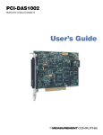
1
CIO-INT32
User’s Manual
Revision 4
September, 2000
Your new Measurement Computing product comes with a fantastic extra —
Management committed to your satisfaction!
Thank you for choosing a Measurement Computing product—and congratulations! You own the finest, and you can now enjoy
the protection of the most comprehensive warranties and unmatched phone tech support. It’s the embodiment of our mission:
To provide data acquisition hardware and software that will save time and save money.
Simple installations minimize the time between setting up your system and actually making measurements. We offer quick and
simple access to outstanding live FREE technical support to help integrate MCC products into a DAQ system.
Limited Lifetime Warranty: Most MCC products are covered by a limited lifetime warranty against defects in materials or
workmanship for the life of the product, to the original purchaser, unless otherwise noted. Any products found to be defective in
material or workmanship will be repaired, replaced with same or similar device, or refunded at MCC’s discretion. For specific
information, please refer to the terms and conditions of sale.
Harsh Environment Program: Any Measurement Computing product that is damaged due to misuse, or any reason, may be
eligible for replacement with the same or similar device for 50% of the current list price. I/O boards face some harsh
environments, some harsher than the boards are designed to withstand. Contact MCC to determine your product’s eligibility for
this program.
30 Day Money-Back Guarantee: Any Measurement Computing Corporation product may be returned within 30 days of
purchase for a full refund of the price paid for the product being returned. If you are not satisfied, or chose the wrong product by
mistake, you do not have to keep it.
These warranties are in lieu of all other warranties, expressed or implied, including any implied warranty of merchantability or
fitness for a particular application. The remedies provided herein are the buyer’s sole and exclusive remedies. Neither
Measurement Computing Corporation, nor its employees shall be liable for any direct or indirect, special, incidental or
consequential damage arising from the use of its products, even if Measurement Computing Corporation has been notified in
advance of the possibility of such damages.
Trademark and Copyright Information
Measurement Computing Corporation, InstaCal, Universal Library, and the Measurement Computing logo are either trademarks
or registered trademarks of Measurement Computing Corporation. Refer to the Copyrights & Trademarks section on
mccdaq.com/legal for more information about Measurement Computing trademarks. Other product and company names
mentioned herein are trademarks or trade names of their respective companies.
© 2000 Measurement Computing Corporation. All rights reserved. No part of this publication may be reproduced, stored in a
retrieval system, or transmitted, in any form by any means, electronic, mechanical, by photocopying, recording, or otherwise
without the prior written permission of Measurement Computing Corporation.
Notice
Measurement Computing Corporation does not authorize any Measurement Computing Corporation product for use
in life support systems and/or devices without prior written consent from Measurement Computing Corporation.
Life support devices/systems are devices or systems that, a) are intended for surgical implantation into the body, or
b) support or sustain life and whose failure to perform can be reasonably expected to result in injury. Measurement
Computing Corporation products are not designed with the components required, and are not subject to the testing
required to ensure a level of reliability suitable for the treatment and diagnosis of people.
(C) Copyright 2000 Measurement Computing Corp.
HM CIO-INT32.lwp
Table of Contents
1.0 INTRODUCTION . . . . . . . . . . . . . . . . . . . . . . . . . . . . . . . . . . . . . . . . . . . . . . . . 1
2.0 SOFTWARE INSTALLATION . . . . . . . . . . . . . . . . . . . . . . . . . . . . . . . . . . . . . 2
3.0 HARDWARE INSTALLATION . . . . . . . . . . . . . . . . . . . . . . . . . . . . . . . . . . . . 2
3.1 BASE ADDRESS . . . . . . . . . . . . . . . . . . . . . . . . . . . . . . . . . . . . . . . . . . . . . . . 2
3.2 INTERRUPT LEVEL SELECT . . . . . . . . . . . . . . . . . . . . . . . . . . . . . . . . . . . 3
3.3 INSTALLING THE CIO-INT32 IN THE COMPUTER . . . . . . . . . . . . . . . . . 5
3.4 CABLING TO THE CONNECTOR . . . . . . . . . . . . . . . . . . . . . . . . . . . . . . . . 6
3.5 SIGNAL CONNECTION . . . . . . . . . . . . . . . . . . . . . . . . . . . . . . . . . . . . . . . . 6
3.6 CONNECTOR DIAGRAM . . . . . . . . . . . . . . . . . . . . . . . . . . . . . . . . . . . . . . . 7
3.7 Z8536 CONTROL & DATA REGISTERS . . . . . . . . . . . . . . . . . . . . . . . . . . . 7
4.0 SPECIFICATIONS . . . . . . . . . . . . . . . . . . . . . . . . . . . . . . . . . . . . . . . . . . . . . . . 9
. . . . . . . . . . . . . . . . . . . . . . . . . . 11
5.0 ELECTRONICS AND INTERFACING
5.1 PULL UP & PULL DOWN RESISTORS . . . . . . . . . . . . . . . . . . . . . . . . . . . 11
5.2 VOLTAGE DIVIDERS . . . . . . . . . . . . . . . . . . . . . . . . . . . . . . . . . . . . . . . . . 13
5.3 LOW PASS FILTERS DE-BOUNCE INPUTS . . . . . . . . . . . . . . . . . . . . . . 15
This page is blank.
1.0 INTRODUCTION
This manual provides technical information for the CIO-INT32. It is intended to be
used with the ZILOG 8536 integrated circuit data sheet and programming manual.
The CIO-INT32 can accept up to 32 vector interrupts and output an interrupt to the
PC. The board contains two Z8536 chips each of which accepts up to 16 independent
inputs that can be used to generate interrupts from bit patterns or individual bit states
or transitions.
The interrupt outputs from two X8536 chips can be ANDed by an on-board jumper.
Many other functions can be performed by the CIO-INT32 including digital pattern
recognition, counting with six, 16-bit counters, and up to 40 bits of digital I/O.
The 16-bit counters can be set up independently or chained together in groups of
three.
The CIO-INT32 is shipped with InstaCalTM, a package of software for installation and
testing of the board
In addition, the board can be supported by the Universal LibraryTM which provides
programming support for all Windows languages.
The CIO-INT32 has a pair of Z8536 I/O chips interfaced to the ISA bus. All of its I/O
lines are accessible through a 50-pin header connector. The I/O pins of an Z8536 are
TTL levels. Connections to the board typically use the C50FF-# cable and the
CIO-MINI50 terminal board.
1
2.0 SOFTWARE INSTALLATION
In order to easily test your installation, it is recommended that you install InstaCal, the
installation, calibration and test utility that was supplied with your board. Refer to the
Software Installation Manual for information on the initial setup, loading, and
installation of InstaCal and optional Universal Library software.
3.0 HARDWARE INSTALLATION
3.1 BASE ADDRESS
The CIO-INT32 employs the PC bus for power, communications and data transfer.
As such it draws power from the PC, monitors the address lines and control signals
and responds to it's I/O address, and it receives and places data on the 8 data lines. If
enabled, it has interrupt capability.
The BASE address is the most important user selectable bus related feature of the
CIO-INT32. The base address is the location that software writes to and reads from
when communicating with the CIO-INT32.
The base address switch is the means for setting the base address. Each switch
position corresponds to one of the PC bus address lines. By placing the switch down,
the CIO-INT32 address decode logic is instructed to respond to that address bit.
A complete address is constructed by calculating the HEX or decimal number which
corresponds to all the address bits
the CIO-INT32 has been instructed
to respond to.
For example, shown to the right are
address 9 and 8 ON, all others
OFF.
Address 9 = 200H (512D) and
address 8 = 100H (256D), when
added together they equal 300H
(768D).
2
Certain address are used by the PC, others are free and may be used by the
CIO-INT32 and other expansion boards. We recommend BASE = 300H (768D) be
tried first.
HEX
RANGE
000-00F
020-021
040-043
060-063
060-064
070-071
080-08F
0A0-0A1
0A0-0AF
0C0-0DF
0F0-0FF
1F0-1FF
200-20F
210-21F
238-23B
23C-23F
270-27F
2B0-2BF
Table 1. PC I/O Addresses
FUNCTION
HEX
RANGE
8237 DMA #1
2C0-2CF
8259 PIC #1
2D0-2DF
8253 TIMER
2E0-2E7
8255 PPI (XT)
2E8-2EF
8742 CONTROLLER (AT)
2F8-2FF
CMOS RAM & NMI MASK (AT)
300-30F
DMA PAGE REGISTERS
310-31F
8259 PIC #2 (AT)
320-32F
NMI MASK (XT)
378-37F
8237 #2 (AT)
380-38F
80287 NUMERIC CO-P (AT)
3A0-3AF
HARD DISK (AT)
3B0-3BB
GAME CONTROL
3BC-3BF
EXPANSION UNIT (XT)
3C0-3CF
BUS MOUSE
3D0-3DF
ALT BUS MOUSE
3E8-3EF
PARALLEL PRINTER
3F0-3F7
EGA
3F8-3FF
FUNCTION
EGA
EGA
GPIB (AT)
SERIAL PORT
SERIAL PORT
PROTOTYPE CARD
PROTOTTYPE CARD
HARD DISK (XT)
PARALLEL PRINTER
SDLC
SDLC
MDA
PARALLEL PRINTER
EGA
CGA
SERIAL PORT
FLOPPY DISK
SERIAL PORT
The CIO-INT32 BASE switch may be set for address in the range of 000-3F8 so it
should not be hard to find a free address area for you CIO-INT32. Once again, if you
are not using IBM prototyping cards or some other board which occupies these
addresses, then 300-31F HEX are free to use.
Addresses not specifically listed, such as 390-39F, are free.
3.2
INTERRUPT LEVEL SELECT
If the software you are writing employs interrupt service routines, you will need to
select and enable interrupts from the CIO-INT32 to the PC bus.
The table below lists typical IRQ assignments. The IRQs described as
UNASSIGNED are typically available to you.
3
NAME
NMI
IRQ0
IRQ1
IRQ2
IRQ3
IRQ4
IRQ5
IRQ6
IRQ7
Table 2. Available IRQs
DESCRIPTION
NAME
DESCRIPTION
PARITY
IRQ8
REAL TIME CLOCK (AT)
TIMER
IRQ9
RE-DIRECTED TO IRQ2 (AT)
KEYBOARD
IRQ10
UNASSIGNED
RESERVED (XT)
IRQ11
UNASSIGNED
INT 8-15 (AT)
COM OR SDLC
IRQ12
UNASSIGNED
COM OR SDLC
IRQ13
80287 NUMERIC CO-P
HARD DISK (AT)
IRQ14
HARD DISK
LPT (AT)
FLOPPY DISK
IRQ15
UNASSIGNED
LPT
Note: IRQ8-15 are AT only
The CIO-INT32 may assert interrupts either:
1.
2.
3.
From an external source brought to the connector.
Individually from each Z8536 for 16 external interrupt lines per chip
Chained as a set of 32 interrupt lines.
Choose a chained or unchained scheme by selecting chained (W) or not chained
(W/O) at the INT PRIORITY jumper.
Choose the source of the interrupt to be routed to the PC bus using the INT SRC
jumper. If the Z8536s are chained, you must choose 1 (Chip 1 or Chip 2).
4
The interrupt output from the Z8536 or connector must be routed to the PC bus. The
interrupt jumper allows you to choose a PC interrupt in the range 2 through 7.
There is no information in this manual describing how to write or use an interrupt
service routine.
3.3
INSTALLING THE CIO-INT32 IN THE COMPUTER
Turn the power off.
Remove the cover of your computer. Please be careful not to dislodge any of the
cables installed on the boards in your computer as you slide the cover off.
Locate an empty ISA expansion slot in your computer.
Push the board firmly down into the expansion bus connector. If it is not seated fully
it may fail to work and could short circuit the PC bus power onto a PC bus signal.
This could damage the motherboard in your PC as well as the CIO-INT32.
3.4
CABLING TO THE CONNECTOR
CIO-INT32 has a pair of Z8536 I/O chips interfaced to the PC bus, with all its I/O
lines accessible through a 50 pin header connector. The I/O pins of an Z8536 are
TTL level.
The CIO-INT32 connector is accessible through the PC/AT expansion bracket. The
connector is a standard 50 pin header connector. The C50FF-# cable and a screw
terminal board, the CIO-MINI50 provide easy access for wiring to the board through
50 12-22 AWG screw terminals on a 4" X 4" terminal board.
3.5
SIGNAL CONNECTION
All the digital outputs inputs on the CIO-INT32 connector are TTL. TTL is an
electronics industry term, short for Transistor Transistor Logic, which describes a
standard for digital signals which are either at 0V or 5V(nominal).
Under normal operating conditions, the voltages on the Z8536 pins range from near 0
volts for the low state to near 5.0 volts for the high state. The current handling
capability of these inputs / outputs is limited to a few milliamps. This is typical of
TTL devices.
5
The voltages and currents associated with external devices range from less than a
hundred mA at a few volts for a small flash light bulb to 50 Amps at 220 volts for a
large electric range. Attempting to connect either of these devices directly to the
CIO-INT32 would destroy the I/O chip.
In addition to voltage and load matching, digital signal sources often need to be
de-bounced. A complete discussion of digital interfacing will be found in the section
on Interface Electronics in this manual.
IMPORTANT NOTE
The Z8536 digital I/O chip initializes all ports as inputs on power
up and reset. A TTL input is a high impedence input. If you
connect another TTL input device to the Z8536 it will probably be
turned ON every time the Z8536 is reset, or, it might be turned OFF
instead. Remember, and Z8536 which is reset is in INPUT mode.
To safeguard against unwanted signal levels, all devices being controlled by an Z8536
should be tied low (or high, as required) by a 10K resistor.
You will find positions for pull up and pull down resistor packs on your CIO-INT32
board. To implement these, please turn to the section on pull up/down resistors.
6
3.6
CONNECTOR DIAGRAM
The CIO-INT32 I/O connector is a 50 pin header type connector accessible from the
rear of the PC through the expansion backplate. The signals available are direct
connections to a Z8536 digital I/O chip.
FIRST Z8536
BASE + 0, 1, 2
INTA
INTB OUT
SECOND Z8536
BASE + 4, 5, 6
OUT/
If frequent changes to signal connections or signal conditioning is required, please
refer to catalog information on the CIO-MINI50 screw terminal board.
3.7
Z8536 CONTROL & DATA REGISTERS
Each CIO-INT32 is composed of two Z8536 parallel I/O chips. Each chip contains
three data and one control register occupying four consecutive I/O locations.
Complete programming and interface information is included in the Zilog Z8536
manuals.
Control and output of the Z8536 chips is accomplished by I/O writes, status and inputs
may be read from I/O ports.
7
The first I/O address, or BASE ADDRESS, is determined by setting a bank of
switches on the board.
To write to or read from a register in decimal or HEX, the following weights apply:
BIT POSITION
0
1
2
3
4
5
6
7
DECIMAL VALUE
1
2
4
8
16
32
64
128
HEX VALUE
1
2
4
8
10
20
40
80
To write a control word or data to a register, the individual bits must be set to 0 or 1
then combined to form a Byte.
The method of programming required to set/read bits from bytes is beyond the scope
of this manual. It will be covered in most Introduction To Programming books,
available from a bookstore.
In summary form, the registers and their function are listed on the following table.
Each register has eight bits which may constitute a byte of data or eight individual bit
set/read functions.
ADDRESS
BASE + 0
BASE + 1
BASE + 2
BASE + 3
BASE + 4
BASE + 5
BASE + 6
BASE + 7
READ FUNCTION
First Z8536 Processor
Port C Input
Port B Input
Port A Input
Status
Second Z8536 Processor
Port C
Port B
Port A
Status
WRITE FUNCTION
Port C Output
Port B Output
Port A Output
Control
Port C
Port B
Port A
Control
Refer to the Zilog Z8536 manual for programming instructions.
8
4.0 SPECIFICATIONS
Typical for 25°C unless otherwise specified.
Power consumption
+5V Operating
440 mA typical, 720 mA max
Counter/Timer and Parallel I/O
Device
Output High
Output Low
Input High
Input Low
Power-up / reset state
Zilog Z85C36 (2)
2.4 volts min @ -250uA
0.5 volts max @ +3.2 mA
2.0 volts min, 7 volts absolute max
0.8 volts max, -0.3 volts absolute min
Input mode (high impedance)
Configured as Digital Input/Output Ports:
Digital Configuration
4 banks of 8 (Ports A and B), 2 banks of 4
(Port C), programmable by bit or bank as input
or output
Number of channels
40 I/O
Configured as Counter/Timers: (Port A is a Digital I/O port only)
Counter type
Zilog Z85C36
Counter Configuration
6 16-bit counter/timers (Port B - High and Low
nibble - and Port C)
All Trigger (C1-C3 TRIG), Source (C1-C3
IN), Gate (C1-C3 GATE), and Output (C1-C3
OUT) available at user connector.
Clock input frequency
3Mhz max
High pulse width (clock input) 150ns min
Low pulse width (clock input) 150ns min
Trigger pulse width (high,low) 130ns min
Interrupts:
The Z8536 is programmable to generate interrupts based on bit change, pattern
recognition, level or edge triggered, whether configured as a digital I/O port or
counter port. See Z8536 manual for further options.
Interrupts
Interrupt enable
Levels 2 through 7, jumper selectable (IRQ
LEVEL)
Jumper selectable (IRQ LEVEL) and external
(INT ENABLE), active low (pulled high
through resistor).
9
Interrupt sources
Interrupt output
Interrupt priority
Jumper selectable (INT SRC): 8536A interrupt
output, 8536B interrupt output, 8536A OR’ed
with 8536B, external (INT INPUT, positive
edge triggered) or None.
Buffered output for each chip available at user
connector (INTA OUT, INTB OUT).
Jumper selectable (INT PRIORITY): No
priority or 8536A interrupt has priority over
8536B interrupt.
Environmental
Operating temperature range
Storage temperature range
Humidity
0 to 50°C
-20 to 70°C
0 to 90% non-condensing
10
5.0 ELECTRONICS AND INTERFACING
This short, simple introduction to the electronics most often needed by digital I/O
board users covers a few key concepts. They are:
Pull up/down resistors
Voltage dividers.
Low pass filters for digital inputs.
IMPORTANT NOTE
WHEN THE Z8536 IS POWERED ON OR RESET, ALL PINS
ARE SET TO HIGH IMPEDANCE INPUT.
The implications of this is that if you have output devices such as solid state relays,
they may be switched on whenever the computer is powered on or reset. To prevent
unwanted switching and to drive all outputs to a known state after power on or reset,
pull all pins either high or low through a 10K resistor.
To install pull up/down resistor packs, see the following section.
5.1
PULL UP & PULL DOWN RESISTORS
This discussion deals with pull-up/pull-down resistors and Z8536 digital I/O chips on
CIO-INT32 boards.
Whenever the Z8536 is powered on or reset, the control register is set to a known
state.
When used as an output device to control other TTL input devices, the Z8536 applies
a voltage level of 0V for low and 2.5V to 5V for high. It is the output voltage level of
the Z8536 that the device being controlled responds to.
The concept of voltage level of an Z8536 in input mode is meaningless. Do not
connect a volt meter to the floating input of an Z8536. It will show you nothing of
meaning. In input mode the Z8536 is in 'high Z' or high impedance. If your Z8536
was connected to another input chip (the device you were controlling), the inputs of
that chip are left floating whenever the Z8536 is in input mode.
If the inputs of the device you are controlling are left to float, they may float up or
down. Which way they float is dependent on the characteristics of the circuit and the
11
electrical environment; and unpredictable! This is why it often appears that the Z8536
has gone 'high' after power up. The result is that the controlled device gets turned on!
That is why you need pull up/down resistors.
Shown here is one Z8536
digital output with a pull-up
resistor attached.
Z8536
10K
The pull-up resistor provides
a reference to +5V while its
value of 10,000 ohms allows
very little current to flow
through the circuit.
If the Z8536 is reset and
enters high impedance input,
the line is pulled high. At that
point, both the Z8536 AND
the device being controlled
will sense a high signal.
If the Z8536 is in output
mode, the Z8536 has more than enough power to over ride the pull-up resistor's high
signal and drive the line to 0 volts. If the Z8536 asserts a high signal, the pull up
resistor guaranties that the line goes to +5V.
Of course, a pull-down resistor accomplishes the same task except that the line is
pulled low when the Z8536 is reset. The Z8536 has more than enough power to drive
the line high.
The CIO-INT32 boards are equipped with positions for pull-up/down resistors Single
Inline Packages (SIPs). The positions are marked A, B and C and are located beside
the Z8536.
A 10 Kohm, 8-resistor SIP has 10K resistors all connected one side to a single
common point and the other, each to a pin protruding from the SIP. The common line
to which all resistor are connected also protrudes from the SIP. The common line is
marked with a dot and is at one end of the SIP.
The SIP may be installed as pull-up or pull-down. At each location, A, B & C there
are 10 holes in a line. One end of the line is +5V, the other end is GND. They are so
marked. The eight holes in the middle are connected to the eight lines of the port, A,
B, or C.
12
Install and solder the SIP in place. Install the SIP with the common pin (dot) in either
the HI or LO hole, then solder the SIP in place.
A resistor value of 10k (10000 ohms) is recommended. Use other values only if you
have calculated the necessity of doing so.
5.2
VOLTAGE DIVIDERS
If you wish to measure a signal which varies over a range greater than the input range
of a digital input, a voltage divider can drop the voltage of the input signal to the level
the digital input can measure.
A voltage divider takes advantage of Ohm's law, which states,
Voltage = Current * Resistance
and Kirkoff's voltage law which states,
The sum of the voltage drops around a circuit will be equal to the voltage
drop for the entire circuit.
Implied in the above is that any variation in the voltage drop for the circuit as a whole
will have a proportional variation in all the voltage drops in the circuit.
A voltage divider takes advantage of the fact that the voltage across one of the
resistors in a circuit is proportional to the voltage across the total resistance in the
circuit.
13
The trick to using a voltage divider is to choose two resistors with the proper
proportions relative to the full scale of the digital input and the maximum signal
voltage.
The phenomena of dropping the voltage proportionally is often called attenuation.
The formula for attenuation is:
Attenuation = R1 + R2
R2
2 = 10K + 10K
10K
R1 = (A-1) * R2
The variable Attenuation is the proportional
difference between the signal voltage max and the
full scale of the analog input.
For example, if the signal varies between 0 and 20
volts and you wish to measure that with an analog
input with a full scale range of 0 to 10 volts, the
Attenuation is 2:1 or just 2.
For a given attenuation, pick a handy resistor and
call it R2, the use this formula to calculate R1.
Digital inputs also make use of voltage dividers.
For example, if you wish to measure a digital signal that is at 0 volts when off and 24
volts when on, you cannot connect that directly to the CIO-DIO digital inputs. The
voltage must be dropped to 5 volts max when on. The Attenuation is 24:5 or 4.8. Use
the equation above to find an appropriate R1 if R2 is 10K. Remember that a TTL
input is 'on' when the input voltage is greater than 2.5 volts.
IMPORTANT NOTE: The resistors, R1 and R2, are going to
dissipate all the power in the divider circuit according to the
equation Current = Voltage / Resistance. The higher the value of
the resistance (R1 + R2) the less power dissipated by the divider
circuit. Here is a simple rule:
For Attenuation of 5:1 or less, no resistor should be less than 10K.
For Attenuation of greater than 5:1, no resistor should be less than
1K.
The CIO-TERMINAL has the circuitry on board to create custom voltage dividers.
The CIO-TERMINAL is a 16" by 4" screw terminal board with two 37-pin D-type
connectors and 56 screw terminals (12 - 22 AWG). Designed for table top, wall or
rack mounting, the board provides prototype, divider circuit, filter circuit and pull-up
resistor positions which you may complete with the proper value components for your
application.
14
5.3
LOW PASS FILTERS DE-BOUNCE INPUTS
A low pass filter is placed on the signal wires between a signal and an A/D board. It
stops frequencies greater than the cut off frequency from entering the A/D board's
analog or digital inputs.
The key term in a low pass filter circuit is cut-off frequency. The cut-off frequency
is that frequency above which no variation of voltage with respect to time may enter
the circuit. For example, if a low pass filter had a cut off frequency of 30 Hz, the kind
of interference associated with line voltage (60Hz) would be filtered out but a signal
of 25Hz would be allowed to pass.
Also, in a digital circuit, a low pass filter might be used to de-bounce an input from a
momentary contact button pushed by a person.
A low pass filter may be constructed from one resistor (R) and one capacitor (C). The
cut off frequency is determined according to the formula:
Fc =
R=
1
2 *π* R * C
Where π = 3.14...
R = ohms
C = Farads
1
2* π * C * Fc
15
For your notes.
16
For your notes.
17
For your notes.
18
EC Declaration of Conformity
We, Measurement Computing Corp., declare under sole responsibility that the
product:
Part Number
CIO-INT32
Description
Interrupt vector board
to which this declaration relates, meets the essential requirements, is in conformity
with, and CE marking has been applied according to the relevant EC Directives listed
below using the relevant section of the following EC standards and other normative
documents:
EU EMC Directive 89/336/EEC: Essential requirements relating to electromagnetic
compatibility.
EU 55022 Class B: Limits and methods of measurements of radio interference
characteristics of information technology equipment.
EN 50082-1: EC generic immunity requirements.
IEC 801-2: Electrostatic discharge requirements for industrial process measurement
and control equipment.
IEC 801-3: Radiated electromagnetic field requirements for industrial process
measurements and control equipment.
IEC 801-4: Electrically fast transients for industrial process measurement and control
equipment.
Carl Haapaoja, Director of Quality Assurance
Measurement Computing Corporation
10 Commerce Way
Suite 1008
Norton, Massachusetts 02766
(508) 946-5100
Fax: (508) 946-9500
E-mail: [email protected]
www.mccdaq.com