1
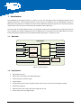
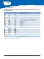
2.1.4
Digital Interface
All digital I/O signals are available on solder-pads. Some of them are routed to other parts (see Table 2-2 for detailed
interconnection information).
Signal
PG13
PG12
PG2
PG3
PG4
SDA
SCL
PG5
PG6
PG7
PG8
PG9
PG10
PG11
PG14
PF14
PF15
PF0
PF1
PF2
PF3
PF4
PF5
PF6
PF7
PPI.CLK1)
PPI.FS1
Alt. Function
UART1RX
UART1TX
SCLK
MISO
MOSI
TMR1
TMR2
TMR3
TMR4
TMR5
TMR6
TMR7
PPI.D0
PPI.D1
PPI.D2
PPI.D3
PPI.D4
PPI.D5
PPI.D6
PPI.D7
Interface
UART
UART
SPI
SPI
SPI
I²C
I²C
GPIO
GPIO
GPIO
GPIO
GPIO
GPIO
GPIO
GPIO
GPIO
GPIO
GPIO
GPIO
GPIO
GPIO
GPIO
GPIO
GPIO
GPIO
PPI
PPI
Connected to
Routed to the UART-USB bridge
Routed to the UART-USB bridge
DIP-switch S2 (usable for bootstrap implementations)
DIP-switch S2 (usable for bootstrap implementations)
push-button SW0
red LED
orange LED
yellow LED
green LED
push-button SW1
push-button SW2
push-button SW3
Table 2-2: Digital interface description
1)
Not available on connector version of the Core Module
ADEV-BF52xC_HUM_V1.1.docx
12