1
International Journal of Emerging Technology and Advanced Engineering
Website: www.ijetae.com (ISSN 2250-2459, ISO 9001:2008 Certified Journal, Volume 3, Issue 5, May 2013)
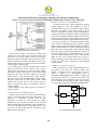
Fig. 2 shows the block diagram of PWM module which
is developed inside the FPGA to drive the motor with the
help of driver circuit. The architecture of the PWM part of
the module consists of two registers, an up counter and on
board clock. One of the two registers is to hold the PWM
duty cycle value, which is the ratio of ON/OFF time
determining the PWM waveform. The other register is to
hold the PWM period data, which controls the duration of a
complete ON/OFF cycle. The values in the two registers
are accessible via serial interfacing and can be updated.
Up and down counters are used to count only when
enabled and the Toggle flip flop toggles every time there is
a final count from any of the enabled counters. When a data
is loaded in the duty cycle register, the down counter
begins to count down from high value to zero. When it
crosses zero, the final count goes high, which toggles the
PWM output to high. Every time the final count goes high
it triggers the duty cycle value to be re-loaded and the Upcounter is enabled and the value is counted from zero to the
high value. Once the Up-counter reaches the final count, it
again triggers the flip-flop to toggle the PWM output.
When a particular duty cycle value is loaded into the
register, the PWM module will generate the corresponding
PWM signal and send it through the on-board General
Purpose Input Output (GPIO) pin. These PWM signals are
then given to drive the motor.
III.
PWM module is implemented inside the FPGA chip in
such a way that it can directly access the GPIO pins, and
thus through the driver card, it drives robot. H-bridge
circuit is used as DC motor driver circuit. The PWM
outputs from the GPIO pins are fed into the H-bridge and
then to drive a DC motor of robot.
The FPGA designs are implemented in Xilinx ISE
software, which provides a variety of performance
analyses, including resource utilization, speed, and power
consumption. The Xilinx performance report is based on
simulations of the hardware design. The interconnection of
PWM module with the FPGA chip has clock frequency of
50 MHz . However we can change the clock across various
frequencies in simulation to investigate the effects on
module performance. The timing analyzer of the ISE
software provides accurate information on delays from
various points, nets and pads inside the FPGA.
The simulation waveforms are measured with the help of
simulation tool and the results show that as per the
command given, signals can be properly selected and
addressed to the particular output port with 40ns delay.
Here for DC motor selection, when '1' and '0' are pressed
then it gives forward output to respective output channel.
Likewise for '0' and '1' , gives reverse output to respective
channel.
IMPLEMENTATION
We have used Xilinx Spartan 3E board and Xilinx
development tool ISE (Integrated Software Environment)
to design the control logic and conducted experimental test.
All the modules are generated in Verilog language. The
experimental test verified the functional correctness of the
hardware module.
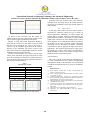
Fig. 5. Simulation result for multiple DC motor control
Output port of FPGA is connected to Digital Signal
Oscilloscope before directly applying to motor. As shown
in the waveform first two channels are for one DC motor
which is in forward direction and last two are for second
DC motor which is in reverse direction. Here medium
speed is selected by applying 50% duty cycle.
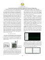
Fig. 4. Experimental Set up
Fig. 4 shows the overall system configuration of the
experimental setup and Spartan 3E FPGA board is the
central piece with wireless end device module and robotic
application with required motor driver circuit attached. The
board has a XC3s500E FPGA chip on it The GPIO pins on
the board are directly connected to the FPGA device.
Fig. 6. Experimental waveform for DC motor logic
337