1
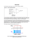
UM0379
User manual
STM3210B-MCKIT and STR750-MCKIT
3-phase motor control power stage
Introduction
This manual describes the MB459B motor control evaluation board. The MB459B is an
AC/AC power converter that generates a three-phase waveform for driving three-phase
motors such as induction motors or PMSM motors.
It includes:
●
An input power stage with voltage rectification and auxiliary power supply,
●
A 7A three-phase inverter based on IGBT and level shifter,
●
A motor connector for linking with the control board,
●
A connector for motors with Hall/encoder and tachometer input.
The MB459B motor control evaluation board can be supplied in two ways:
●
From a single power supply for motors requiring a voltage greater than 18 V;
●
From a dual power supply for motors requiring a voltage less than 18 V.
This manual describes where the various components are located on the motor control
board, and the appropriate settings for driving a PMSM motor or an AC induction motor.
The MB459B board is delivered with the STM3210B-MCKIT and STR750-MCKIT motor
control kits. For more information on these kits, refer to www.st.com.
December 2007
Rev 2
1/21
www.st.com
Contents
UM0379
Contents
1
Hardware layout . . . . . . . . . . . . . . . . . . . . . . . . . . . . . . . . . . . . . . . . . . . . . 3
2
Power supply . . . . . . . . . . . . . . . . . . . . . . . . . . . . . . . . . . . . . . . . . . . . . . . 4
3
Operational amplifier configuration . . . . . . . . . . . . . . . . . . . . . . . . . . . . 5
3.1
Three-shunt current reading configuration . . . . . . . . . . . . . . . . . . . . . . . . . 5
3.2
Single-shunt current reading configuration . . . . . . . . . . . . . . . . . . . . . . . . . 7
3.3
Jumper configuration . . . . . . . . . . . . . . . . . . . . . . . . . . . . . . . . . . . . . . . . . 9
4
Electrical specifications . . . . . . . . . . . . . . . . . . . . . . . . . . . . . . . . . . . . . 10
5
Hardware settings for driving PMSM motors . . . . . . . . . . . . . . . . . . . . 11
6
Hardware settings for driving AC induction motors . . . . . . . . . . . . . . 12
7
Description of jumper and connector settings . . . . . . . . . . . . . . . . . . . 13
8
Schematic diagrams . . . . . . . . . . . . . . . . . . . . . . . . . . . . . . . . . . . . . . . . 17
9
Revision history . . . . . . . . . . . . . . . . . . . . . . . . . . . . . . . . . . . . . . . . . . . 20
2/21
UM0379
1
Hardware layout
Hardware layout
This section illustrates the main connectors of the MB459B motor control board (see
Figure 1), and describes their function.
Figure 1.
MB459B connectors
1
4
3
9
2
7
6
8
5
1.
Motor and board input power stage, auxiliary power supply, and voltage rectification
2.
Prototype area
3.
J3 connector: power supply input
4.
J1 connector: auxiliary supply input
5.
J8 connector: Hall sensors / encoder input
6.
J6 connector: tachometer input for closed-loop controlled AC motors
7.
J5 connector: Three-phase output to motor
8.
J7 motor connector: link to STR75x and to STM3210B-EVAL evaluation board, or other
control board
9.
7A inverter and level shifter
3/21
Power supply
2
UM0379
Power supply
The MB459B motor control evaluation board can be supplied from a single power supply or
from a dual power supply.
●
Single power supply for motors requiring a voltage greater than 18 V
The power is supplied to the J3 connector. The voltage must not exceed 42V DC or
30Veff AC. It supplies both the motor and the motor control board. A 15V DC voltage is
automatically generated for the motor control board logic. However, depending on the
voltage supplied, two cases are possible:
●
–
If the supplied voltage is greater than 35V DC, the W1 jumper must be set in
"HIGH VOLTAGE" position;
–
If the supplied voltage is between 18V and 35V DC, the W1 jumper must be set in
the "<35V ONLY" position.
Dual power supply for motors requiring a voltage less than 18 V
The power for the motor is supplied to the J3 connector, while a separate power supply
for the motor control board logic must be applied to the J1 connector (15V DC, 0.5 A).
Caution:
In the case of dual power supply, the W1 jumper must be removed and the D3 shortcircuit must be unsoldered (this is to avoid having reverse current in the linear
voltage regulator).
Note:
On the J3 connector, the polarity of DC input is not important.
Figure 2 shows where the power supply connectors are located on the board.
Figure 2.
MB459B power supply connectors
1
3
2
1.
J1 connector: 15V DC, 0.5 A power supply input (used in dual power supply mode to
supply the motor control board logic).
2.
J3 connector: motor power supply (in dual power supply mode) or motor plus motor
control board power supply (in single power supply mode). Up to 42V DC or 30Veff AC.
3.
W1 jumper. In single power supply mode, selects the motor voltage; in dual power
supply mode, it must be removed.
4/21
UM0379
3
Operational amplifier configuration
Operational amplifier configuration
The MB459B motor control evaluation board can be configured to run in two current reading
configuration modes:
●
Three-shunt configuration
●
Single-shunt configuration
Single-shunt configuration requires a single op-amp, three-shunt configuration requires
three op-amps, and for compatibility purposes, one of them must be common to the two
configurations.
Jumpers W7, W8 and W9 allow you to set the common op-amp to achieve the compatibility
between single-shunt and three-shunt current reading mode.
The TSV994 used on the motor control board has a 20MHz gain bandwidth and operates
with a single positive supply.
Three-shunt current reading configuration
Figure 3 gives the op-amp configuration for the three-shunt current reading mode. In this
configuration, the alternating signal on the shunt resistor, with positive and negative values,
must be translated to be compatible with the single positive input voltage of the
microcontroller’s analog-to-digital converter used to read the current value.
This means that the op-amp must be polarized in order to obtain on the output a voltage that
makes it possible to measure the symmetrical alternating input signal.
Three-shunt configuration
U
e
shunt
i1
r1
i2
+5V
r3
v
r2
7
Figure 3.
3
+
2
-
6
s
4
3.1
R
r
5/21
Operational amplifier configuration
UM0379
The op-amp is used in follower mode with a gain set by resistors r and R.
G = s / v = (R + r)/r
The relation between the input signal e and the signal v on the positive input of the follower
is:
v = (U/(k*r3) + e/(k*r1))
where k =(1/r1+1/r2+1/r3)
The resistor values implemented on the MB549B board are:
R=5400Ω \ r=1000Ω \ r1=660Ω \ r2=560Ω \ r3=4700Ω
and
U=5V
Therefore, the gain is:
G = 6.4
The response of the op-amp is represented in Figure 4.
Figure 4.
Voltage response in three-shunt configuration
Op_Amp Output
Vout Op_Amp
3.500
3.000
2.500
2.000
Series2
1.500
1.000
0.500
0.000
-0.6
-0.4
-0.2
0
0.2
0.4
0.6
V shunt
With these settings, the output voltage of the op-amp is equal to 1.94V for a nil current.
The peak current that can be measured in this configuration is:
+/- 5A for R_shunt = 0.1ohms
+/- 2.3A for R_shunt = 0.22 ohms
6/21
UM0379
Single-shunt current reading configuration
In the single-shunt current reading configuration, the current sampling is done only when the
value on the shunt resistor is positive.
The only positive value read on the shunt resistor allows to set a higher gain for the op-amp
than the one set in three-shunt mode. However, because the input of the op-amp is not railto-rail, in this configuration also, it is necessary to polarize the it to compensate for this
limitation.
Figure 5 shows the op-amp configuration used in single-shunt configuration.
Figure 5.
Single-shunt configuration
+5V
shunt
U
r1
i1
w
r4
i2
v
7
e
r2
3
+
2
-
6
s
4
3.2
Operational amplifier configuration
r3
R
r
The op-amp is used in follower mode with a gain set by resistors r and R.
G = s/v = (R + r)/r
The relation between the input signal e and the signal v on the positive input of the follower
is:
v = ((U*h)/(k*r4) + f(e))
with:
k =(1/r3+1/(r1+r2)+1/r4)
h=r1/ (r1 +r2)
f(e)=(e*r2)/ (r1 + r2) + (e*r1)/((k*(r1+r2)*(r1+r2))
The resistor values implemented on the MB549B board are:
R=11000Ω \ r=1000Ω \ r1=1130Ω \ r2=1000Ω \ r3=22Ω \ r4=2200Ω
and
U=5V
Therefore, the gain is:
G = 12
7/21
Operational amplifier configuration
UM0379
The response of the op-amp is shown in Figure 6.
Figure 6.
Voltage response in single-shunt configuration
Vout Op_Amp
Op_Amp Output
3.500
3.000
2.500
2.000
1.500
1.000
Series1
0.500
0.000
0
0.1
0.2
0.3
0.4
0.5
0.6
V shunt
In this configuration, the output voltage of the op-amp is equal to 3.16V when the maximum
peak current that is measured in R_shunt is reached:
+ 5A for R_shunt = 0.1Ω or + 2.3A for R_shunt = 0.22Ω
8/21
UM0379
Jumper configuration
Based on the two current reading configurations for single-shunt and three-shunt, the final
configuration of the common op-amp is summarized in Figure 7.
Figure 7.
Common op-amp configuration
+5V
W8
shunt
7
e
1_Shunt
3
+
2
-
6
s
4
3.3
Operational amplifier configuration
W7
W9
U
3_Shunts
9/21
Electrical specifications
4
UM0379
Electrical specifications
Table 1 provides the maximum ratings for the MB459B motor control board.
Table 1.
Motor control evaluation board electrical specifications
Parameter
Maximum ratings
Motor types
Three-phase PMSM or AC motor
Main input voltage (J3)
42V DC or 30 Veff AC
Auxiliary input voltage (J1)
15V DC, 0.5A
Maximum output current on motor phases (J5)
7A
The maximum current allowed on the motor phases is mainly dependent on the shunt
resistor value and op-amp gain. For further information, see Section 3: Operational amplifier
configuration on page 5.
10/21
UM0379
5
Hardware settings for driving PMSM motors
Hardware settings for driving PMSM motors
To drive the PMSM motor, you must simply ensure that the MB459B motor control board is
driven by a control board that outputs the six signals required to drive the three-phase power
stage. The MB469B STR75x evaluation board provided in the STR750-MCKIT or the
STM3210B-EVAL evaluation board provided with the STM3210B-MCKIT are perfectly
suited for this task.
To drive any other generic high voltage PMSM motor, you must ensure that:
●
your PMSM motor is connected on the motor control board in place of the PMSM motor
provided, on the J5 and J8 connectors,
●
the motor phases are connected to the board on the J5 connector,
●
the encoder from the PMSM motor is connected to the board on the J8 connector
For example, for the Shinano PMSM motor provided with the STR750-MCKIT and the
STM3210B-MCKIT the connections are listed in Table 2.
Table 2.
Jumper settings for a PMSM motor (default settings)
Jumper
Settings for the supplied
SHINANO 24V PMSM motor
Settings for a generic high
voltage PMSM motor
W1
“< 35V Only”
“< 35V Only” or “ HIGH VOLTAGE”
W4
Present
W5
Not present
W6
Present
W7
Present and set to default position of silk-screen printing
W8
Present
W9
Present
W10
Present
W11
Present
W12
Not present
W13
Not present
W14
Not present
W15
Not present
W16
Present and set to reverse position of silk-screen printing
W17
Present
W18
Present
W19
Present
11/21
Hardware settings for driving AC induction motors
6
UM0379
Hardware settings for driving AC induction motors
To drive an AC induction motor, you must ensure that:
●
The motor control evaluation board is driven by an adapted control board that outputs
the six signals required to drive the three-phase power stage,
●
The AC induction motor is connected on the motor control board in place of the PMSM
motor,
●
The AC induction motor phases are connected to the board on the J5 connector,
●
The tacho generator is connected to the board on the J6 connector.
Table 3.
Jumper settings for an AC Induction motor
Jumper
12/21
Settings for a generic AC motor with tachometer feedback
W1
“< 35V Only” or “ HIGH VOLTAGE”
W4
Present
W5
Not present
W6
Present
W7
Present and set to default position of silk-screen printing
W8
Present
W9
Present
W10
Present
W11
Present
W12
Present
W13
Not present
W14
Not present
W15
Not present
W16
Present - any position
W17
Not present
W18
Not present
W19
Not present
UM0379
7
Description of jumper and connector settings
Description of jumper and connector settings
Table 4.
Jumper descriptions
Jumper
Selection
Description
“ HIGH VOLTAGE”
Motor supply is greater than 35V DC or 25Veff AC.
“< 35V Only”
Motor supply is less than 35V DC or 25Veff AC.
Not present
Power motor supply is separate from motor control
circuit.The motor control circuit must be supplied with
15V DC (0.5A) on J1 connector. In this case, the D3
short-circuit must be removed (unsoldered) from the
PCB. Refer to Section 2: Power supply for details.
Present
Connects R3 shunt resistor to T2 IGBT source for the
three shunt configuration.
Not present
Disconnects R3 from T2 IGBT source for the single
shunt configuration.
Present
Connects the T2 IGBT source to R4 shunt resistor for the
single shunt configuration.
Not present
Disconnects the T2 IGBT source from R4 shunt resistor
for the three shunt configuration.
Present
Connects the output of thermal comparator on shutdown to the pin 2 input of the L6386 MOS-driver. In such
cases, the thermal protection can also generate an
emergency stop forcing the Fault signal to low.
Not present
Disables feedback of thermal comparator on L6386
MOS-driver.
Set to default position of
silk-screen printing
Selects the input polarization of Phase B current op-amp
for the three shunt configuration.
Set to reverse position of
silk-screen printing
Selects the input polarization of Phase B current op-amp
for the single shunt configuration.
Present
Sets the input resistor of Phase B current op-amp for
three shunt configuration.
Not present
Sets the input resistor of Phase B current op-amp for
single shunt configuration.
Present
Sets the gain resistor of Phase B current op-amp for
three shunt configuration.
Not present
Sets the gain resistor of Phase B current op-amp for
single shunt configuration.
Set to default position of
silk-screen printing
Connects R5 shunt resistor to T6 IGBT source for the
three shunt configuration.
Set to reverse position of
silk-screen printing
Connects the T6 IGBT source to R4 shunt resistor for the
single shunt configuration.
W1
W4
W5
W6
W7
W8
W9
W10
13/21
Description of jumper and connector settings
Table 4.
UM0379
Jumper descriptions (continued)
Jumper
Selection
Description
Present
Connects the output of diagnostic comparator to the
Fault/MC EMGCY input of microcontroller pin P1.10
Not present
Disconnects the output of diagnostic comparator from
the Fault/MC EMGCY input of microcontroller pin P1.10
Present
Connects the tachometer signal to Measure Phase A /
TIM2_TI1 input P0.03. In that case, W17 is not present
(removed).
Not present
Disconnects the tachometer signal from Measure Phase
A / TIM2_TI1 input P0.03.
Present
The 3.3V Pow supply connected to Vdd_m is used to
supply the microcontroller board connected on pin 26 of
the motor control connector J7.
Not present
Vdd_m is not connected to the 3.3V Pow of power board.
Present
The 5V supply connected to Vdd_m, is used to supply
the microcontroller board connected on pin 26 of the
motor control connector J7.
Not present
Vdd_m is not connected to the 5V of the power board.
Present
Uses the 5V of the microcontroller board to supply the
power board via the motor control connector J7.
Not present
The 5V of the power board is not supplied by the
microcontroller board.
Set to default position of
silk-screen printing
The +Vdd_m is used to supply the Hall sensor or
encoder
Set to reverse position of
silk-screen printing
The +5V is used to supply the Hall sensor or encoder
Present
Enables Hall1/A+ on Measure Phase A/ TIM2_TI1 input
P0.03
Not present
Disables Hall1/A+ for Measure Phase A/ TIM2_TI1 input
P0.03
Present
Enables Hall2/B+ on Measure Phase B/ TIM2_TI2 input
P1.03
Not present
Disables Hall2/B+ for Measure Phase B/ TIM2_TI2 input
P1.03
Present
Enables Hall3/Z+ on Measure Phase C/ TIM0_TI1 input
P0.01
Not present
Disables Hall3/Z+ for Measure Phase C/ TIM0_TI1 input
P0.01
W11
W12
W13
W14
W15
W16
W17
W18
W19
14/21
UM0379
Description of jumper and connector settings
Table 5.
Name
Connector pinout descriptions
Reference
2
J1
J2
J3
2
1
1
2
3
1
J4
12
Optional 15V DC, 0.5A input connector to supply the motor control
board logic separately from the motor power stage.
1) 15V DC power supply
2) Vss power
15V DC output connector to supply auxiliary board. This connector is
not mounted.
1) 15 V DC power supply
2) VSS power
Up to 42V DC or 30Veff AC power supply input connector.
1) Earth/ground
2) Power input (AC/DC)
3) Power input (AC/DC)
BEMF daughter board connector
1) Phase A
2) Not connected
3) Phase B
4) Not connected
5) Phase C
6) Not connected
7) Bus voltage
8) Not connected
9) +5V
10) +Vdd_m
11) Vss board
12) PWM Vref
Motor three-phase output.
1) Motor phase C
2) Motor phase A
3) Motor phase B
4) DC bus middle point (may be used for two-phase motors)
5) Earth
5
J5
1
J6
1
Description/pinout
2
1
Tachometer input connector for AC motor speed loop control.
1) Tachometer bias (0.6 V)
2) Tachometer input
15/21
Description of jumper and connector settings
2
34
Reference
1
Name
Connector pinout descriptions (continued)
33
Table 5.
J7
1
J8
16/21
UM0379
5
Description/pinout
Motor control connector
1) EMERGENCY STOP ---------------- 2) GND
3) PWM-1H ---------------------------------- 4) GND
5) PWM-1L ---------------------------------- 6) GND
7) PWM-2H ---------------------------------- 8) GND
9) PWM-2L --------------------------------- 10) GND
11) PWM-3H ------------------------------- 12) GND
13) PWM-3L ------------------------------ 14) HV BUS VOLTAGE
15) Current PHASE A ---------------- 16) GND
17) Current PHASE B----------------- 18) GND
19) Current PHASE C----------------- 20) GND
21) NTC BYPASS RELAY ---------- 22) GND
23) DISSIPATIVE BRAKE PWM - 24) GND
25) +V Power ---------------------------- 26) Heatsink temperature
27) PFC Sync --------------------------- 28) Vdd_m
29) PWM Vref --------------------------- 30) GND
31) Measure Phase A ---------------- 32) GND
33) Measure Phase B ---------------- 34) Measure Phase C
Hall sensors/ encoder input connector
1) Hall sensor input 1 / encoder A+
2) Hall sensor input 2 / encoder B+
3) Hall sensor input 3 / encoder Z+
4) 5V DC power supply
5) VSS board
UM0379
8
Schematic diagrams
Schematic diagrams
The MB459B motor control evaluation board schematics are split into two sheets:
●
Sheet 1/2 Current Measurement (Figure 8), shows the op-amp wiring and
configuration, the encoder/ Hall sensor adaptation, the tacho input stage and the motor
control connector wiring.
●
Sheet 2/2 Power Switch (Figure 9), shows the power converter with its associated level
shifter and all auxiliary power supplies.
The version of the board described in this manual is MB459-B01. The board version
information can be found on a sticker on the component side of the PCB (the visible one), on
the bottom left edge of the board when reading the serigraphy.
The changes on this version of the board compared with the previous version MB459-B00
are summarized below:
●
Operational amplifiers have changed, TSV994 replacing TSH24.
●
The value of capacitors C37, C42, and C47 has increased from 10pF to 100pF.
●
The value of resistors R13, R23 and R52 has decreased from 2.2kΩ to 1.8kΩ.
●
The D3 diode is now short-circuited.
●
The board can also be driven by the STM3210B-EVAL board.
17/21
1
+Vdd_m
W14
2
2
2
4
6
8
10
12
14
16
18
20
22
24
26
28
30
32
34
All resistors 1%
+3.3V Pow
W13
1
1
3
5
7
9
11
13
15
17
19
21
23
25 1
27
29
31
33
34CONT
J7
R29
1K
C38
33P
560
R33
4K7
R31
R51
1K
C46
33P
2
R49
560
R45
1K
R39
4K7
R40
560
C41
33P
+5V
I Low Phase B
W7
I Low Phase C
Heatsink Temperature
+5V
1
1K
R58
R48
560
R59
470
I High Phase C
HV Bus
R57
22
R56
2K2
+5V
4K7
R55
I High Phase B
2
W8
I Low Phase A
1
3
-
C37
9
2K7
R60
8
TSV994
PWM_Brake
R68
2
+5V
47K
W15
PWM Vref
Measure Phase A
Measure Phase B
R66
47K
R67
47K
TP39
1
1K
R54
47K
R71
47K
R70
TP43
TP25
47K
R69
TP42
TP29
1K
R62
1K
R38
TP28
TP40
W9
R61
5K6
2K7
R27
2
TP38
2K7
R28
100P
Measure Phase C
1
TSV994
U6C
+
Current Phase A
Current Phase B
Current Phase C
Fault
-
U6A
+
100N
C43
4μ7 25V
2K7
R47
7
TSV994
C11
C47
100P
2
3
10
2K7
R50
R30
560
-
2K7
R46
C42
100P
6
+5V
R41
560
U6B
+
+Vdd_m
+Vdd_m
PWM_2L
PWM_Brake
PWM_3L
PWM_3H
100N
2
3
4
5
Hall3/Z+
+5V
GND
TP31
PWM_3LBuf
PWM_3HBuf
PWM_2LBuf
PWM_2HBuf
PWM_1LBuf
PWM_1HBuf
_ PWM_Brake
Wrapping Area
R65
1K
-
220P
R35
39K
U6D
+
C62
13
3
14
R
2
3
Size
A4
Date:
U21A
6
4μ7
100N
C51
TP33
R79
10K
D17
BAS16
D18
BAS16
R75
10K
TS372
MB 459
Wednesday, September 12, 2007
Document Number
MCU Application Lab
+Vdd_m
2
2
2
Sheet
1
of
2
R ev
B-01
Drawn by: JM CHARRETON
Vincent ONDE
Approved by:
Measure Phase A
Measure Phase B
2
W19
W18
W17
W12
TP32
C54
2N2
1
C56
1
1
1
10P
Measure Phase C
R73
100
T7
BC817
R72
10K
TP35
TP37
TP36
C57
10P
C58
4K7
10P
R77
4K7
+Vdd_m
C55 100N
R74
0(NC)
1
Thermal Protection
R78
+
U20A
-
25V
74HC09
100N
C60
3
74HC09
8
74HC09
3-Phase power stage MB459
C59
100N
U21C
U21B
C14
+Vdd_m
+5V
2
1
10
9
5
4
Organisation name:
2
1
J6
1K
R64
+5V
R82
4K7
Title:
R81
4K7
C61
100N
50V
Vref
R80
TSH24
W16
C52
330P
R32
10K 12
+5V
1
2
Heatsink Temperature
R34
10K
+Vdd_m
Kontek-Comatel
1
Hall2/B+
J8
11
Hall1/A+
74HC09
U21D
Temp
13
12
74HCT7007
5 U8C 6
74HCT7007
9 U8D 8
74HCT7007
11 U8E 10
74HCT7007
13 U8F 12
74HCT7007
PWM_1L 3 U8B 4
PWM_2H
2
C50
1 U8A
74HCT7007
PWM_1H
+5V
Current Phase C
BAR43
D14
Current Phase B
BAR43
D16
TP41
+Vdd_m
Current Phase A
BAR43
D15
HALL SENSOR /
ENCODER
5
4
11
+5V
14
7
14
7
4K7
TACHO
METER
R76
4K7
18/21
8
Figure 8.
4
I High Phase A
Schematic diagrams
UM0379
Schematics sheet 1/2: current measurement
J1
100μF
25V
C15
22N
10μ
25V
C20
BAS16
fus5x20
4
FB
VDD
IN
3
+
High Voltage
TP8
SOURCE
DRAIN
RES
SET
1.5KE18P
OUT
OUT
OUT
OUT
2
3
6
7
100μF
25V
1μ
25V
C53
TP34
C3
TP3
R10
1K5 D2
+15V
U3 VIPER12AS-E
0.23V
GREEN LED
LD1
C22
3
2
Y
C2
4N7
Y
C1
4N7
R
Title:
Size
Custom
Date:
MB 459
Wednesday, September 12, 2007
Document Number
MCU Application Lab
3-Phase power stage MB459
Organisation name:
Z1
1μ
C16
U1
2
L7805CP or CV
+3.3V Pow
C18
100N
1
WA627-003
Mounted on
30°C/W Heatsink
X2
Sheet
2
of
2
C7
1000μF
200V
WIRING
2
C8
1000μF
200V
1
2.54 linebar
D3
1
C45
+15V
10μF
35V
C9
C33
PWM_3LBuf
1.8K 2.2nF
R23
PW M_2HBuf
PWM_2LBuf
1.8K 2.2nF
R13 C27
1
7
6
5
4
3
2
1
7
6
5
4
3
2
1
LIN
U5
GND
CIN
DIAG
VCC
HIN
SD
LIN
U4
GND
CIN
DIAG
VCC
HIN
SD
LIN
VBOOT
L6386D
R20 1K
GND
LVG
NC
NC
OUT
HVG
VBOOT
L6386D
R12 1K
GND
LVG
NC
NC
OUT
HVG
VBOOT
14
8
9
10
11
12
13
14
8
9
10
11
12
13
14
C39
22
R14
220
D13
R44
BAS16
D10
R19
22
220
R17
BAS16
D11
R15
TP27
1μ
25V
C29
C32
22N
TP18
1μ
25V
C30
22
220
R8
BAS16
220
R9
BAS16
D6
R11
22
R6
D7
TP19
1μ
25V
C25
C26
22N
TP9
1μ
25V
C24
TP14
T1
TP23
R4
0R22
5%
T4
STGF7NC60HD
T3
STGF7NC60HD
PWM Vref
+5V
+Vdd_m
Bus Voltage
Phase C
with 1.27 & 2.54 footprint
5V, 15V, GND, Max CURRENT: 50mA
PWM_Brake Pin
WRAPPING AREA
1
W6
1N
10μF
35V
C12
1.8K 2.2nF
R52 C48
PWM_3HBuf
7
6
5
4
3
2
U7
GND
CIN
DIAG
VCC
HIN
SD
L6386D
R43 1K
GND
LVG
NC
NC
OUT
HVG
8
9
10
11
12
13
1μ
25V
C44
22N
TP26
1μ
25V
220
BAS16
220
R36
BAS16
D12
R42
22
R37
22
C40
TP30
R25
100
C21
Temp
I High Phase B
W5
W4
C49
10N
2
R53
100
R5
0R22
5%
W10
C13
10N
400V
I Low Phase B
10N
C36
C10
10N
400V
to be soldered
STGF7NC60HD
C5
10N
400V
STGF7NC60HD
I High Phase C
T6
STGF7NC60HD
T5
10N
R7 120R
TP6
Phase B
Phase C
Phase C
Phase B
I Low Phase C
to be soldered
TP24
C31
10N
I Low Phase A
R3
0R22
5%
TP16
Phase A
Phase A
To be
soldered
W2
X4 KM100-1
I High Phase A
R16
100
TP10
Mounted on 2.9°C/W KM100-1
AAVID Thermalloy Heatsink
NTC2
Mounted on 2.9°C/W KM100-1
AAVID Thermalloy Heatsink
TP13
T2
+5V
STGF7NC60HD
2
R26
47K
1N
C34
+15V
10μF
35V
C4
PWM_1HBuf
PWM_1LBuf
TP7
Mounted on 2.9°C/W KM100-1
AAVID Thermalloy Heatsink
TP21
Vref
6
5
1K
R24
1N
C28
+15V
Bus Voltage
Phase B
1
+5V
TP20
R63
3K3
R22
8.2K
R21
470K
HV Bus
R18
470K
+
2 7
U20B
TS372
TP_0
TP2
C35
47N
TP_0
TP1
CTN10K
To
Heatsink
Phase A
TP44
W11
NC (short)
TP12
R1
47K
1W
R2
47K
1W
Thermal Protection
Fault
2
1μ
25V
U2
2
L7815CP or CV C17
1
2
3
4
5
6
7
8
9
10
11
12
J4
+5V
TP5
R ev
B-01
WA627-003
Mounted on
30°C/W Heatsink
X3
BZW50-120B
50V
Drawn by: JM CHARRETON
Vincent ONDE
Approved by:
1μ
25V
C19
1mH (nc)
L2
1
W3
BZW50-120B
Z2
35V Max
TP4
D1
3
TP17
1.5KE36A
W1
Z3
BZW50-100B
C6
100N
400V
TOKO 8 R H B
PANASONIC E L C 0 9 D 102 F
1mH
L1
1
SW1: Must Be on 35V Max
for 24V External Supply
D4
STBR608
U10 LD1117D33
JACK 15V
1
2
3
Stick Supply
J2
MKDSN 1,5/2-5,08
2
1
D8
F1
3.15A TEMP
TV1505
Mounted on 17°C/W
AAVID Thermalloy
heatsink
X1
NTC1 SG170 (4R)
TP11
Z4
BZX84C15
TP22
1
2
3
To be soldered for AC voltage doubler configuration
This drawing may not be reproduced by a third party unless permission is obtained in writing from ST MICROELECTRONICS
+5V
GND
+15VDC
D5
STTH112U
STTH112U
D9
C23
220N
AC/DC input
GMKDS 3/3-7,62
4
J3
MSTBA2,54/5-G-5,08
+ 4
1 -
4
5
2
J5
8
7
6
5
1
2
C 1
A
2
B 3
GND
1
3
MOTOR
BEMF_Daughter Board
3
2
1
2
1
1
1
2
TP15
Figure 9.
3
UM0379
Schematic diagrams
Schematics sheet 2/2: power switch
19/21
Revision history
9
UM0379
Revision history
Table 6.
20/21
Document revision history
Date
Revision
Changes
7-Feb-2007
1
Initial release.
17-Dec-2007
2
Added list of changes to the MB459B board compared with the
previous version in Section 8: Schematic diagrams.
Update for release of STM32B-MCKIT motor control kit.
UM0379
Please Read Carefully:
Information in this document is provided solely in connection with ST products. STMicroelectronics NV and its subsidiaries (“ST”) reserve the
right to make changes, corrections, modifications or improvements, to this document, and the products and services described herein at any
time, without notice.
All ST products are sold pursuant to ST’s terms and conditions of sale.
Purchasers are solely responsible for the choice, selection and use of the ST products and services described herein, and ST assumes no
liability whatsoever relating to the choice, selection or use of the ST products and services described herein.
No license, express or implied, by estoppel or otherwise, to any intellectual property rights is granted under this document. If any part of this
document refers to any third party products or services it shall not be deemed a license grant by ST for the use of such third party products
or services, or any intellectual property contained therein or considered as a warranty covering the use in any manner whatsoever of such
third party products or services or any intellectual property contained therein.
UNLESS OTHERWISE SET FORTH IN ST’S TERMS AND CONDITIONS OF SALE ST DISCLAIMS ANY EXPRESS OR IMPLIED
WARRANTY WITH RESPECT TO THE USE AND/OR SALE OF ST PRODUCTS INCLUDING WITHOUT LIMITATION IMPLIED
WARRANTIES OF MERCHANTABILITY, FITNESS FOR A PARTICULAR PURPOSE (AND THEIR EQUIVALENTS UNDER THE LAWS
OF ANY JURISDICTION), OR INFRINGEMENT OF ANY PATENT, COPYRIGHT OR OTHER INTELLECTUAL PROPERTY RIGHT.
UNLESS EXPRESSLY APPROVED IN WRITING BY AN AUTHORIZED ST REPRESENTATIVE, ST PRODUCTS ARE NOT
RECOMMENDED, AUTHORIZED OR WARRANTED FOR USE IN MILITARY, AIR CRAFT, SPACE, LIFE SAVING, OR LIFE SUSTAINING
APPLICATIONS, NOR IN PRODUCTS OR SYSTEMS WHERE FAILURE OR MALFUNCTION MAY RESULT IN PERSONAL INJURY,
DEATH, OR SEVERE PROPERTY OR ENVIRONMENTAL DAMAGE. ST PRODUCTS WHICH ARE NOT SPECIFIED AS "AUTOMOTIVE
GRADE" MAY ONLY BE USED IN AUTOMOTIVE APPLICATIONS AT USER’S OWN RISK.
Resale of ST products with provisions different from the statements and/or technical features set forth in this document shall immediately void
any warranty granted by ST for the ST product or service described herein and shall not create or extend in any manner whatsoever, any
liability of ST.
ST and the ST logo are trademarks or registered trademarks of ST in various countries.
Information in this document supersedes and replaces all information previously supplied.
The ST logo is a registered trademark of STMicroelectronics. All other names are the property of their respective owners.
© 2007 STMicroelectronics - All rights reserved
STMicroelectronics group of companies
Australia - Belgium - Brazil - Canada - China - Czech Republic - Finland - France - Germany - Hong Kong - India - Israel - Italy - Japan Malaysia - Malta - Morocco - Singapore - Spain - Sweden - Switzerland - United Kingdom - United States of America
www.st.com
21/21