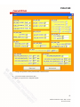
1
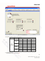
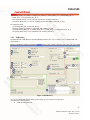
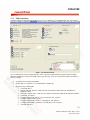
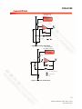
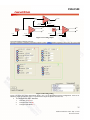
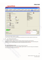
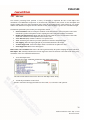
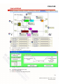
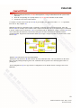
ISD61S00 ISD61S00 Evaluation System User’s Manual 1 Publication Release Date: May 5, 2010 Revision 61.0031 ISD61S00 1. Getting Started ...................................................................................................................4 1.1 Install the ISD61S00 Evaluation System ......................................................................... 4 2. Evaluation Board Overview ...............................................................................................7 2.1 USB Controller and Power Sources ................................................................................. 7 2.2 ISD61S00 and Related Circuitry ...................................................................................... 8 2.3 Clare DAA........................................................................................................................ 9 2.4 Discrete DAA ................................................................................................................. 10 3. ISD61S00 Software Utility Overview .............................................................................12 3.1 PCM & PLL ................................................................................................................... 12 3.2 Voice Prompt.................................................................................................................. 14 3.2.1 Keystrokes to Re-order VPs.................................................................................... 15 3.3 Reserved Memory .......................................................................................................... 15 3.4 Voice Macro ................................................................................................................... 16 3.5 Path Config..................................................................................................................... 18 3.6 Memory Map .................................................................................................................. 20 3.7 Archive and Clean .......................................................................................................... 22 3.8 DTMF Detect ................................................................................................................. 23 3.9 Tone/DTMF Gen ............................................................................................................ 25 3.10 FSK Detect ................................................................................................................. 27 3.11 FSK Generation .......................................................................................................... 29 3.12 Register Map............................................................................................................... 31 3.13 Analog ........................................................................................................................ 32 3.14 Demo .......................................................................................................................... 36 3.15 AEC/LEC.................................................................................................................... 38 3.16 AGC ............................................................................................................................ 45 3.17 GPIO/INT ................................................................................................................... 48 3.17.1 GPIO ....................................................................................................................... 48 3.17.2 Interrupt................................................................................................................... 49 3.18 Detect .......................................................................................................................... 50 3.18.1 CAS detect .............................................................................................................. 51 3.18.2 ATD ........................................................................................................................ 52 3.18.3 Ring Detect ............................................................................................................. 54 3.18.4 CPT Detect .............................................................................................................. 55 3.18.5 VD ........................................................................................................................... 56 3.18.6 Demo ....................................................................................................................... 57 4. Evaluation Board Control ................................................................................................59 4.1 Audio Cmds.................................................................................................................... 59 4.2 Digital Cmds .................................................................................................................. 61 5. Board Schematic ..............................................................................................................64 5.1 USB Controller and Power Sources ............................................................................... 64 5.2 ISD61S00 and Related Circuitry .................................................................................... 65 5.3 Clare DAA...................................................................................................................... 66 2 Publication Release Date: May 5, 2010 Revision 61.0031 ISD61S00 6. 5.4 Discrete DAA ................................................................................................................. 67 Revision History ..............................................................................................................68 3 Publication Release Date: May 5, 2010 Revision 61.0031 ISD61S00 1. Getting Started The ISD61S00 is a feature chip for the security and telephony industry. The ISD61S00 evaluation system is an integrated tool kit which enables users to evaluate the features of ISD61S00 including: a powerful macro scripting ability to facilitate audio prompting in a multi-language environment and simple address-free recording and playback; and telephony based data communications including DTMF detection and generation, FSK modem functions from 75-1200 baud, CAS and CPT (Call Progress Tone) detection and ring detection. 1.1 Install the ISD61S00 Evaluation System Please follow the steps below to set up the evaluation system: 1. Install the ISD61S00 software utility before plugging the EV board onto PC. 2. After the ISD61S00 software utility is properly installed, plug the EV board onto PC. 1. Users shall see a message popped up; select „No, not this time‟, and then click „Next‟. Figure 1-1 Install USB Driver - 1 2. Select „install from a list or specific location (Advanced)‟, and then click „Next‟. Figure 1-2 Install USB Driver - 2 3. Click „Browse‟. 4 Publication Release Date: May 5, 2010 Revision 61.0031 ISD61S00 Figure 1-3 Install USB Driver - 3 4. USB driver is located in the ISD61S00 software utility installation folder, which by default is "c:\Program Files\ISD61SXX Evaluation System\Driver"; Click „OK‟. Figure 1-4 Install USB Driver - 4 5. Users shall then see the installing of USB driver in progress. Figure 1-5 Install USB Driver - 5 6. After the installation of USB driver, reset the USB by unplugging and plugging the board. 5 Publication Release Date: May 5, 2010 Revision 61.0031 ISD61S00 Figure 1-6 Install USB Driver - 6 6 Publication Release Date: May 5, 2010 Revision 61.0031 ISD61S00 2. Evaluation Board Overview Figure 2-1 below is the ISD61S00 Evaluation board. The board has 4 main areas: 1. USB Controller and Power Sources 2. ISD61S00 and Related Circuitry 3. Clare DAA 4. Discrete DAA Figure 2-1 ISD61S00 Evaluation Board 2.1 USB Controller and Power Sources The board could be powered by USB power (A) or an external 5V power (B), as determined by the jumper J6 (C) or 3 AAA batteries by the jumper J9 (?). VR1 (D) is a 5V-to-3V regulator to provide the needed 3V for the ISD61S00. Or, users could also power the board by a 3V power source via the on-board banana jack (E); the jumper J5 (F) must be removed if this is the case. 7 Publication Release Date: May 5, 2010 Revision 61.0031 ISD61S00 The evaluation system is controlled by an on-board USB controller W681308 (G). Users can capture the controlling signals between the USB controller and the ISD61S00 on the on-board headers (H). To reset the USB controller, users could either press the RESB button (I) or unplug and plug the USB cable (A). The on-board USB controller has its own microphone (J) and speaker (K) interfaces. Figure 2-2 USB Controller and Power Sources 2.2 ISD61S00 and Related Circuitry ISD61S00 (A) is clocked by the crystal or the external clock source. There is a 12.288MHz crystal (B) on the board. The jumper J21 (C) must be removed if users want to clock the ISD61S00 by an external clock source. ISD61S00 is a ROM-less part, which uses external serial flash as the storage media. On board there are a DIP-8 socket (E) and a flash socket footprint (F, socket not included); users can select either one by the jumpers J29 (G) and J30 (H). For the DIP-8 socket, flash memory will be soldered on an SOIC adaptor board so that users can replace the flash easier. For the flash socket, users can turn the board into a flash programmer by soldering the flash socket. Around the ISD61S00 are the related connectors and circuitries: I2S interface (I) shares the GPIO pins 4 ~9; by default these pins are pull-up input pins; to set them as I2S users have to set the corresponding PORT_AF (port alternate function) registers. J31 and JAUX (J) are the pin-header and jack for Aux-out. Aux-out is a single-ended voltage output, which needs an external amplifier to drive the speaker. J25 and JAUXSPK (S) are the pin-header and jack for Aux-out amplified. The ISD8101 U10 takes the single end voltage as input and drives the speaker with differential voltage by JAUXSPK. 8 Publication Release Date: May 5, 2010 Revision 61.0031 ISD61S00 o If user wants to drive speaker by external amplifier ISD8101, user may put jumpers on J43 and J44 2-3 to turn on the ISD8101. J27 and 3.5mm Jack (K) are the pin-header and jack for the device speaker driver outputs. MK1 (L) is the on-board microphone, which is configured as a single-ended microphone input. To use the microphone, user can put jumper on J19 (N) 5-6, J38 1-2 and J39 1-2 (R). o If users want to record messages via Aux-in, users can put jumpers on J19 (N) 1-2 & 3-4, remove the jumper on J19 (N) 5-6, and then record through the jack phone connector JADCIN (O). J36 and JTI1IN (P) are the pin-header the jack connector of the TI1P/TI1N. J14 is the keypad connector for standalone operation. The keypad consists of A 4 x 4 kay pad. A uC to talk to the main board. A display for Caller ID. To reset the ISD61S00, users can press the RESET button (Q) Figure 2-3 ISD61S00 and Related Circuitry 2.3 Clare DAA With the Clare DAA configuration, the phone signal (A) goes to the on-board Clare CPC5622 (B) to talk to the ISD61S00. The Clare CPC5622 (B) converts the 2-wire phone signal (TIP and RING) to 4 wires (TI and PO) and processes the controlling signals including the Hook Control, Hook Detection, Loop Detection, Ring Detection, and Pulse Dial. This simple configuration reduces the number of discrete components as in the Discrete DAA. 9 Publication Release Date: May 5, 2010 Revision 61.0031 ISD61S00 To use the Clare DAA, users need to switch SW1 (C) as in Figure 2-5 . The switch SW1 (C) of Clare DAA is a counterpart of the switch SW11 of Discrete DAA. Figure 2-4 Clare DAA AVDD R103 100K AVDD SW1 C1 + 10UF C2 0.1UF CLARE_RINGHALF CLARE_HOOK_CTRL CLARE_RINGFULL CLARE_HOOK_DET CLARE_LOOP_DET CLARE_PO+ CLARE_POCLARE_TI1P CLARE_TI1N 1 3 5 7 9 11 13 15 17 19 21 23 2 4 6 8 10 12 14 16 18 20 22 24 GPIO15/RDET/TI3P GPIO14/RDET GPIO13/RDET GPIO12 GPIO11 GPIO10 PO+ POTI2P TI2N TI1P TI1N GPIO15/RDET/TI3P GPIO14/RDET GPIO13/RDET GPIO12 GPIO11 GPIO10 PO+ POTI2P TI2N TI1P TI1N DIL switch 12 SMT CKN6109-ND / SDA12H1SBD Figure 2-5 Switch of Clare DAA 2.4 Discrete DAA Unlike the Clare DAA, the Discrete DAA configuration uses discrete components to convert the phone line (A) and process the controlling signals including the Hook Control, Hook Detection, Loop Detection, Ring Detection, and Pulse Dial. For details of Discrete DAA configuration, please refer to section 5.4 Discrete DAA. To use the Discrete DAA, users need to swicth SW11 (B). The switch SW11 (B) of Discrete DAA is a counterpart of the switch SW1 of Clare DAA. 10 Publication Release Date: May 5, 2010 Revision 61.0031 ISD61S00 Figure 2-6 Discrete DAA 11 Publication Release Date: May 5, 2010 Revision 61.0031 ISD61S00 3. ISD61S00 Software Utility Overview There is an example project named I61SXX_Sample. This section introduces the ISD61S00 software utility panel by panel based on this example project. To open the example project: launch the ISD61S00 software utility. On the menu bar, click „Project‟ -> „Open‟; users can find the example project in "c:\Program Files\ISD61SXX Evaluation System\I61SXX_Sample". There are three subfolders in the project folder: BinFiles: where the compressed Voice Prompts are stored. WavFiles: where the re-sampled and de-compressed Voice Prompts are stored. WavSrc: where wave sources of Voice Prompts are stored. 3.1 PCM & PLL Users configure the Digital Audio Interface (PCM/I2S) and the Clock Generation on this panel. ISD61S00 has a digital audio interface consisting of two physical transitive/receive channels; both channels share common clock and synchronization. With digital audio, ISD61S00 can be configured as master (ISD61S00 generates clock and frame sync) or slave (ISD61S00 accepts clock and frame sync). The digital audio interface has two modes; In I2S mode, PCM interface conforms to the I2S digital audio interface convention. In PCM mode, data transfer is synchronized to the rising edge of the frame sync signal. For register details please refer to the design guide, section 8.4 Digital Audio Interface Control. transmitters 2 physical channels mode setting receiver Figure 3-1 PCM/I2S Control 12 Publication Release Date: May 5, 2010 Revision 61.0031 ISD61S00 Figure 3-2 below shows the block diagram of the clock generation. The PLL is mainly used to multiply the external input clock by a fractional number (the f2 = R * f1 in the diagram). The dividers before and after the PLL are optional for users to get the frequency within a certain range. The target IMCLK is 24.576MHz. For register details please refer to the design guide, section 8.3 Clock Generation and PLL. ADC PLL Prescaler REG44[4] Master Clock Prescaler REG40[4:2] XTALIN 0 f1 1 DAC PLL f 2=R*f 1 f2 f/4 fPLL 1 f/N 0 IMCLK = 24.576MHz f/2 DPLL PLL BLOCK f2 = 98.304MHz DPLL REG3[7:4] GPIO[13] MCLK Source REG44[6] BCLK_RATE REG3[2:0] f/N CODEC_FS REG3[3] f/M f/N GPIO13 AF bit OPCLK_DIV REG40[2:0] Master/Slave Mode REG50[4] 1 0 FS Digital Audio Interface BCLK Figure 3-2 Clock Generation and PLL Figure 3-3 Clock and PLL Setting 13 Publication Release Date: May 5, 2010 Revision 61.0031 ISD61S00 3.2 Voice Prompt Voice prompts are pre-recorded audio of any length, from short words, phrases or sound effects to long passages of music. These Voice Prompts can be played back in any order as determined by the users and applications. A voice prompt consists of two components: (1) An index pointing to the pre-recorded audio. (2) Pre-recorded audio. Before adding voice prompts, first set the default sampling rate (A) and compression algorithm (B). To add voice prompts, follow the steps below: (1) Set sampling rate (C) and compression algorithm (D) for the VPs you are going to add. Users can change the individual VP‟s sampling rate (E) and/or compression algorithm (F) later when evaluating the quality. (2) Add voice prompts (G). (3) Repeat steps (1) & (2). (4) Change the VP tags (H) if needed; by default, the tags are the filenames. (5) Re-order the VPs if needed; select VP by clicking on the square (I), and click on the up/down arrows (J) to re-order the VPs. If users change the clock configuration, they must re-compress all VPs (K) because clock setting is part of the VP compression. Users can evaluate the VPs through PC or EV board: Through PC (L): i. Original voice prompts before re-sampling & compression. ii. Re-sampled but not yet compressed voice prompts. iii. Compressed voice prompts. Through EV board: 1. Plug in the EV board and the „Play to device‟ button (M) shows up. The added voice prompts will appear on the „Voice Macro‟ screen for voice macro script programming. K G C L A D M B Figure 3-4 Voice Prompt screen I H E F J 14 Publication Release Date: May 5, 2010 Revision 61.0031 ISD61S00 3.2.1 Keystrokes to Re-order VPs Besides the up/down arrows (J), users can also use the keystrokes to re-order the VPs: Select VP by clicking on the square (I) Press M on keyboard and a pop-up box shows up. Enter the new VP # to re-order the VP. Figure 3-5 Re-order VPs 3.3 Reserved Memory Recording Memory Pointer (RMP) divides the ISD61S00 memory space into two blocks: Reserved Memory, Recording Memory. RMP is a two-byte address pointer pointing to a 4kbyte memory sector which is the first sector available for message recordings. Memory between address zero and the RMP pointer is considered the Reserved Memory for pre-recorded audio (Voice Prompts), pre-programmed macro scripts (Voice Macros), digital read/write access for other applications (User Data), and memory sectors reserved for the first sector of the reserved messages (Reserved Sectors). The memory between the RMP and the end of memory is considered the Recording Memory allocated for recording messages (Message Recordings). Figure 3-6 Example of ISD61S00 Memory Map On the „Reserved Memory‟ screen, users reserve memory sectors for message recordings: Empty messages (A): o An Empty Message is an empty 4kByte memory sector reserved for message recordings. An SPI record command pointing to the Empty Message starts the message recording and will continue to 15 Publication Release Date: May 5, 2010 Revision 61.0031 ISD61S00 record to the free memory sectors located in Recording Memory if the message recording is over 4kByte. Re-recordable messages (B): o Users can have a default message when reserving the memory sectors for a message recording. For a re-recordable message, the first sector will be allocated in „Reserved Sectors‟; the rest of the message will be allocated in „Recording Memory‟. Please note only ADPCM, (D)uLaw, and PCM compressions are supported for reserved messages, not EnhancedADPCM or VBR. To record (or playback) a message, the microcontroller simply issues a record (or playback) command with starting address pointing to the reserved initial address. The reserved messages are also listed on the „Voice Macro‟ screen for voice macro script programming. Memory sectors can also be assigned in Reserved Memory for digital read/write access for other application tasks (User Data). To reserve empty memory sectors, click the button „Add Reserved Memory‟ (C) and then adjust the „Number of Sectors‟ (D). To reserve (import) existing data, click the button „Add Data‟ (E); the file size will be shown on „number of sectors‟ (F). A B C E Figure 3-7 Reserved Memory D 3.4 Voice Macro F Voice Macro is a powerful scripting feature integrated into the ISD61S00. Voice Macro editor enables users to create scripted commands to play voice prompts (A), play reserved messages (B), insert silence (C), power down the ISD61S00 (D), and configure the ISD61S00 (E) such as setting play or record paths. As mentioned earlier, the voice prompts (A) are from the „Voice Prompt‟ panel, and the reserved messages (B) are from the „Reserved Memory‟ panel, respectively. Each VM is assigned a tag and an index, where it can be executed with a single SPI command referring to the index. There are 3 special Voice Macros: Index 0: VM0, Power-On Initialization (POI). o Executed automatically when power supplied or when a high pulse applied on RESET pin. Index 1: VM1, Power-Up (PU). 16 Publication Release Date: May 5, 2010 Revision 61.0031 ISD61S00 o Executed automatically when received power-up command. Index 2: VM2, Power-Up (WAKEUP). o Executed automatically when woke up from a GPIO interrupt. POI, PU, and WAKEUP Macros allow users to customize how the part emerges from power-on, power-up, and wake-up conditions. There are two special VM commands: FINISH (F) and WAIT INT (G). FINISH (F): o Finish the voice macro and exit. Voice Macros must be ended in either FINISH or PD (power down). WAIT INT (G): o Wait until current play command finishes before executing next macro instruction. E A I B C F D H Figure 3-8 Voice Macro The ISD61S00 has a built-in command buffer so that consecutive commands can be executed one after another seamlessly. However, some commands won‟t go through command buffer; therefore, they won‟t wait. Users may refer to the design guide; section 10 SPI Commands, Table 10-2, for details. In table 10-2 users may see that some commands can be executed regardless the status bit-1 CBUF_FULL (command buffer full). WAIT_INT (H) is used whenever a command in a voice macro intends to wait to be executed until previous play command finishes. A typical example will be adjusting volume in a voice macro. Commands for adjusting volume won‟t go through the command buffer; therefore, they will be executed immediately. Below is an example where the volume is immediately decreased when VP_A starts to play. Play VP_A Decrease Volume 17 Publication Release Date: May 5, 2010 Revision 61.0031 ISD61S00 Play VP_B Finish. If users want to decrease volume after VP_A finishes, the voice macro should be modified as below: Play VP_A WAIT_INT Decrease Volume Play VP_B Finish. Please note that the commands in a Voice Macro are executed sequentially, and all voice macros shall be ended with PD or FINISH to finish the voice macro. Users shall see a warning message if the software detects a voice macro not ended with PD or FINISH. 3.5 Path Config This panel helps users to configure the ISD61S00 Signal Path. The path diagram has 4 main parts: 1. Air input/output (microphone and speaker) 2. Phone-line input/output, and the DTMF/FSK generation and detection. 3. Mixers 4. Compression and de-compression Figure 3-9 below shows a typical phone signal path: This site to the other site: Microphone (A) -> ADC (B) -> Lrin (C) -> AEC (D) ->Asout (E) -> MIC (F) -> Arin (G) -> LEC (H) -> Lsout (I) -> DAC (J) -> PO (K) The other site to this site: TI1 (A) -> ADC (B) -> Lrin (C) -> LEC (D) ->Asout (E) -> TI (F) -> Arin (G) -> AEC (H) > Lsout (I) -> DAC (J) -> SPK (K) To enable or disable a path portion, users simply click on the related function block, and the software automatically switches to the corresponding panel. For example, to disable the ADC (B), users just click on the ADC block, and then the software will switch to the CODEC panel as in Figure 3-10 . Users then uncheck the Air CODEC (L) to disable the ADC. (Please note that ADC and DAC share the hardware circuitry, so the ADC and DAC will be turned on or off at the same time). Similarly, to tune the AEC (D) users just click on the AEC block, and the software utility automatically switches to the AEC panel as in Figure 3-11 . For register details of AEC and LEC, please refer to design guide, section 8.18 Air and Line CODEC. To change the of gain of Lrin (C), Asout (E), MIC (F) … etc, users just click on the function block and then a gain setting bar shows up as the Figure 3-12 . The software utility has built in some default path settings as in Figure 3-13 for users‟ reference. To try a setting, users simply double-click on it. Or, users can click on it, modify the setting as needed, and then click the „Write CFG‟. 18 Publication Release Date: May 5, 2010 Revision 61.0031 ISD61S00 A 1 B C K 3 F D E J F I H G 2 A B K F C D I J E F G H 4 Figure 3-9 Path Config Figure 3-10 CODEC L 19 Publication Release Date: May 5, 2010 Revision 61.0031 ISD61S00 Figure 3-11 AEC Parameters Figure 3-12 Gain Setting Figure 3-13 Default Path Settings 3.6 Memory Map Memory Map generates the programming file to be burned into the ISD61S00 memory. The programming file is a binary file with .mem extension. On this panel users will see how each VP, VM, and message is assigned an address and/or index. To activate the process, click on „Create Programming File‟ (A). The left hand side displays the memory map (B). 20 Publication Release Date: May 5, 2010 Revision 61.0031 ISD61S00 On the right hand side, the Memory Protection (C) decides how you want the memory contents protected. ISD61S00 provides three kinds of protection mechanisms: Read Protection: o Once enabled, digital-read command is not effective in those protected area. Write Protection: o Once enabled, digital-write and memory-erase commands are not effective in those protected area. Chip-Erase Protection: o Once enabled, chip-erase command is not effective. If both Chip Erase Protect (CEP) and Write Protect (WP) are checked, it will lock the content from beginning of the memory to PMP, preventing ISD61S00 from any further modification. The check boxes under „Project Information‟ (D) allow users to add project information to the programming file. If users check the users comment box, whatever they type in the comment window will be appended to the end of the project information. If the EV board is connected to PC, the „Burn Device‟ button (E) will be effective. Once the programming file is created, users can click „Burn Device‟ to download the programming file into the ISD61S00. Please note that „Date‟ (F) is part of the project, so clicking on the „Create Programming File‟ (A) may change the project contents even though users don‟t change anything. When users open an existing project, the memory map will be loaded automatically. C B D F Figure 3-14 Memory Map A E 21 Publication Release Date: May 5, 2010 Revision 61.0031 ISD61S00 3.7 Archive and Clean Under project menu there are two very useful functions. 1. Archive and, 2. Clean These two functions are used to backup your project files and clean up unnecessary files. They are useful when you want to send an ISD61S00 project to other people. The archiving function duplicates a project to an archive directory with exactly same project name and structure, and changes the project links to point to this directory so that all paths are stored relative to the project directory. For example, if you create an ISD61S00 project in a network share folder which is, say, mapped to T drive, you cannot just send this project to other people because “T” drive means nothing to other people. By archiving the project, that project is now self contained and can just be copied to another machine or to backup. Figure 3-15 Archive The Clean function deletes the contents in the BinFile and WavFile directories as they can be regenerated. The WavFile directory contains wave files of re-sampled and de-compressed voice prompts. The BinFile directory contains files of compressed voice prompts. When a project is created, three sub-directories are created: BinFiles: where the compressed VPs are stored. WavFiles: where the re-sampled and de-compressed VPs are stored. WavSrc: where wave source of VPs are stored. A project file has the prj extension. The binary programming file for the project has mem extension. A header file with txt extension is also included for C language firmware programming. 22 Publication Release Date: May 5, 2010 Revision 61.0031 ISD61S00 Figure 3-16 Open a Project 3.8 DTMF Detect DTMF Detect can decode the digits in off-hook state and display them in (A). To run the function, follow the steps below and refer to Figure 3-17: (1) Press the “GO” (B) button to load the default registers and the new registers will update to the panel immediately. Then the EVB will decode the default digits automatically and display them in (A). (2) Press the “Clear” (C) button to clear the decoded digits in (A) if needed; send more digits from other telephone through telephone line. And the decoded digits are also shown in (A). (3) If the decoded digits are not correct, tune the timing (D) (E) (F) according to Figure 3-18, tune the threshold (G), DTMF_TC (H) and Freq Deviation(I). And then Press “Write CFG” (J) button to change the conditions. Press “Read CFG” (K) to confirm the conditions if needed. (4) Send the digits again. (5) If the decoded digits are still not correct, repeat steps (3) & (4). According to Figure 3-18, users can also monitor the immediate states: DTMF_RDY(L), DTMF_STATE(M) and DTMF_RX_DATA(N). 23 Publication Release Date: May 5, 2010 Revision 61.0031 ISD61S00 Figure 3-17 DTMF Detect screen 24 Publication Release Date: May 5, 2010 Revision 61.0031 ISD61S00 Figure 3-18 DTMF Detector Acquisition timing 3.9 Tone/DTMF Gen Tone/DTMF generator operates in three different modes: 1. DTMF mode 2. Programmable mode 3. Continuous mode If user set the DTMF_MODE to 1, the function is in the DTMF mode. If user set the DTMF_MODE to 0, the function is in the programmable and continuous mode. The setting of DTMF_MODE bit explained as following table: Mode TONE_FREQ_A TONE_FREQ_B TONE_LEVEL_A TONE_LEVEL_B TONE_ON_TIME TONE_OFF_TIME TONE_LENGTH Continuous User define User define Set: 0 Set: 0 DTMF Don‟t care User define User define Programmable User define User define User define Number of digits in tone index registers. Number of tones to generate TONES TO GEN Don‟t care Digits to send Don‟t care For the DTMF mode, (1) Checking GEN_EN (A), DTMF_MODE (B) and CLK_EN (C) (2) Setting TONE_ON_TIME (D), TONE_OFF_TIME (E), TONE_LEV_A (H) and TONE_LEV_B (I). (3) To input the number of DTMF digits in the TONE_LENGTH (J) and the numeral you want to generate in TONES TO GEN (K). (4) Clicking Write CFG (L), the DTMF tone of the TONES TO GEN (K) would be generated. 25 Publication Release Date: May 5, 2010 Revision 61.0031 ISD61S00 A B C D F H E G I J K L Figure 3-19 Tone/DTMF Gen The frequency of DTMF is defaulted as following table: Column frequency 697 Hz Row Frequency 770 Hz 852 Hz 941 Hz 1209 Hz 1336 Hz 1477 Hz 1633 Hz 0x01 hex 0x02 hex 0x03 hex 0x0D hex 1 2 3 A 0x04 hex 0x05 hex 0x06 hex 0x0E hex 4 5 6 B 0x07 hex 0x08 hex 0x09 hex 0x0F hex 7 8 9 C 0x0B hex 0x0A hex 0x0C hex 0x00 hex * 0 # D For Programmable mode, (1) Checking GEN_EN (A) and CLK_EN (B) 26 Publication Release Date: May 5, 2010 Revision 61.0031 ISD61S00 (2) Setting TONE_ON_TIME (D), TONE_OFF_TIME (E), TONE_FREQ_A (F), TONE_FREQ_B (G), TONE_LEV_A (H) and TONE_LEV_B (I). (3) To input the number of tones you want to generate in TONE_LENGTH (J). (4) Click the Write CFG (L), the tone would be generated for TONE_LENGTH (J) times For continuous mode, (1) Checking GEN_EN (A) and CLK_EN (B) (2) Setting TONE_ON_TIME (D) and TONE_OFF_TIME (E) to zero (3) Setting TONE_FREQ_A (F), TONE_FREQ_B (G), TONE_LEV_A (H) and TONE_LEV_B (I) (4) Clicking Write CFG (L). The continuous tone would be generated. 3.10 FSK Detect The ISD61S00 has a FSK Detector supporting Bell202, Bell103, ITU-T V.21 and ITU-T V.23 standard FSK. The control panel is A B I J U K V O C D E L F G H P M N Q S R T Figure 3-20 FSK Detect Area 1 is for general FSK detect control register setting. Area 2, 3 and 4 are for demo only. (1) FSK Detect control registers: FSK detection parameter: 27 Publication Release Date: May 5, 2010 Revision 61.0031 ISD61S00 FSKD_CDET (C), FSK_SYNC(D), FSKD_THRES(E), FSKD_TC(F), FSKD_ENERGY_HI(G), FSKD_ENERGY_LO(H), FSKD_MODE(K), FSKD_JUDGE(L). FSKD_FIFO_CTRL: control the FSK detection FIFO, to clear the FIFO, click „CLEAR‟(M) and Press „Write CFG‟, the FSK detector FIFO will reset to a clean state. FSKD_Status: shows the FSK detect CDB and current demodulated data bit. FSKD_FIFO_STATUS: shows current FSK detection FIFO status. FSKD_FIFO_DOUT: current FIFO head. To receive type 1 FSK CID message, the procedure is: Step1: click FSK_EN(A) and FSK_INT_MD(B) to checked state. Step2: configure FSKD_CDET(C), this value at least greater than 3. Step3: configure FSKD_SYNC(D), this vale at least greater than 2. Step4: configure FSKD_THRES(E), control the FSK detector sensitivity. The smaller, the more sensitive. Step5: configure FSKD_TC(F), FSKD_ENERGY_HI(G) and FSKD_ENERGY_LO(H). These 3 parameters only used when Bell202 or V.23 is chose. For other FSK spec (Bell103 and V.21), these 3 parameters has no effect. Step6: configure FSK_PARITY_EN(I), PARITY_TYPE(J), SPEC_SEL(K). Step7: configure FSK_CMP_CNT(L) Step8: clear FIFO by click „CLEAR‟(M), set the FIFO_LEN(N) to decide INT occur depth. Step9: Press „GO‟. Step10: configure SPEC_SEL(K) again. Step11: Press „Write CFG‟ Step12: When FSK detector receives the message, it will display the message in the text box. (2) Caller ID Detection : Demo area for Bell202 CID detection, the procedure is: Step1: click Bell202 Caller ID(T) in the right down configuration area. Step2: Press „GO‟ button in 2nd area. Step3: When ISD61S receive a session of FSK CID signal, the Name(U) and Number(V) will display. (3) FSK DETECION DEMO : Demo for FSK generator and receive with Detector, the procedure is: Step1: select FSK spec in the SPEC_SEL(K) text box and press „Write CFG‟. Step2: prepare a text file with message in it. Step3: Press „GO‟(S) in 3rd area. The GUI will ask user to provide a file and then control ISD61S FSK generator to send this text in FSK spec selected in SPEC_SEL(K). When FSK detector receives the message, it will display the message in the text box. (4) Dedicate area for security product. The procedure is: Step1: Select ACK Tone timing(R). Step2: Key in the dial number in the Dial Number text box(Q). Step3: Press „GO‟(P) and GUI will control ISD61S to communicate with a main machine. 28 Publication Release Date: May 5, 2010 Revision 61.0031 ISD61S00 3.11 FSK Generation The FSK Generation supporting Bell202, Bell103, ITU-T V.21 and ITU-T V.23 standard FSK. The control panel is G H I J A B C D E L K F M N R O P Q S T Figure 3-21 FSK Generation Area 1 is FSK Encode control setting and status. Area 2 is specific customized mark and space baud rate setting. When SW_MODE(M) is checked, the SPEC_SEL(K) has no effect. Area 3 is for demo the transmit text with area 1 and area 2 setting. To quickly select a FSK_GEN_DEMO: Double click (T), if speaker is on, user should hear 1270Hz tone. To generate type 2 FSK signal: 1. Click FSK_EN(A) 2. Click PACKAGE_EN(B) to 1, this will insert start bit before data and stop bit behind data to construct a frame. 3. Click FIFO_HALF_INT(C), INT will occur when Transmit FIFO depth reaches half full condition. 4. Click FSK_TX_ON(D) 5. Configure FSK_STOP_SEL(E). 1 for two stop bits, 0 for 1 stop bit. 6. Configure FSK generation gain(F). 7. Configure FSK_PARITY_EN(G). 1 add parity bit. 0 no parity bit. 8. Configure FSK PARITY_TYPE(H). 0 for odd parity. 1for even parity. 9. Click IIR_EN(I) to 1 29 Publication Release Date: May 5, 2010 Revision 61.0031 ISD61S00 10. 11. 12. 13. Configure BAUD_110(J) to 1 if baud rate 110 is required. Configure SPEC_SEL(K) to target FSK standard. Prepare a text file with transmit content. Press GO(R) a File input dialog will show 14. Select the file and Press „Load‟. The line interface will send FSK signal based on the text file. 15. To repeat transmit, press GO(R) again. To use SW Mode to generate type 2 FSK signal: 1. Click FSK_EN(A) 2. Click PACKAGE_EN(B) to 1, this will insert start bit before data and stop bit behind data to construct a frame. 3. Click FIFO_HALF_INT(C), INT will occur when Transmit FIFO depth reaches half full condition. 4. Click FSK_TX_ON(D) 5. Configure FSK_STOP_SEL(E). 1 for two stop bits, 0 for 1 stop bit. 6. Configure FSK generation gain(F). 7. Configure FSK_PARITY_EN(G). 1 add parity bit. 0 no parity bit. 8. Configure FSK PARITY_TYPE(H). 0 for odd parity. 1for even parity. 9. Click IIR_EN(I) to 1 10. Click SW_MODE(M) 11. Configure MARK_FREQ(O) 12. Configure SPACE_FREQ(P). 13. Configure BAUDRATE(Q). 14. Prepare a text file with transmit content. 15. Press GO(R) a File input dialog will show 30 Publication Release Date: May 5, 2010 Revision 61.0031 ISD61S00 16. Select the file and Press „Load‟. The line interface will send FSK signal based on the text file. 17. To repeat transmition, press GO(R) again. 3.12 Register Map The Register Map shows the register status. There are two ways to modify the register values: (1) Modify many register values at the same time: To modify the value in the register map (A) at different addresses, click Write CFG (B), the modified value would be written into these registers. Clicking Read CFG (C), the register map shows the value you just modified. The color of modified value would be changed. The illustration is in the textbox (D). (2) Modify one register value at a time: to choose one address (E) and modify the value (F), button (V) would show the address and register name. Clicking Write Register (G), the register map (A) shows the changed value. Clicking Read Register (H) to check if the value is written into register. 31 Publication Release Date: May 5, 2010 Revision 61.0031 ISD61S00 I M P J K L N Q O R S A T D V B C E U G F H Figure 3-22 Register Map There are two register storages in the panel. Clicking the CFGA (I) button, the register values can be saved to register A. Clicking the CFGB (J) button, the register values can be saved to register B. If you want to recover register A status, click ACFG (K) button. If you want to recover register B status, click BCFG (L) button. Clicking the Print BCFG (M) button, the text area (T) shows the different register values from register B to current configurations. Clicking the Print ACFG (N) button, the text area (T) shows the different register values from register B to current configurations. The CFG ALL (O) button shows the register values in the text area (T) except the read only registers. The Print BA (P) button shows the changed register values from register B to register A in the text area (T). The Print AB (Q) button shows the changed register values from register A to register B. The NON-ZERO (R) button shows the non-zero register values. The Print Style (S) button can choose the style of address and register value showing in the text area (T). Clicking the Config Screen (U) button, GUI would jump to Path Config screen. 3.13 Analog The Analog section contains the setting of MIC, SPK, PSTN line input and output, and AUX out. The microphone interface can operate on 3 modes: 1) Microphone Voltage gain mode; 2) Microphone Current gain mode; 3) Auxiliary input mode. The reference voltage and internal resistor can be configured by GUI. 32 Publication Release Date: May 5, 2010 Revision 61.0031 ISD61S00 Voltage Gain Mode MIC_MODE = 000 Programmable Bias Generator MIC_BIAS[2:0] MIC_RES[7:4] R3 2.436Vp + MCP Vout to ADC - R2 MIC_GAIN[7:4] MC O 250 R1 V ADC R 1 2 VMCP R1 MIC_GAIN[7:4] MCGND A Figure 3-23 Voltage Gain Mode Current Gain Mode MIC_MODE = 010 or 011 Programmable Bias Generator MIC_BIAS[2:0] MIC_RES[7:4] R3 2.436Vp + A MCP Vout to ADC - R2 REXT S1 MIC_GAIN[7:4] MC O 250 VADC REXT 250 for mode 011 IS MCGND A VADC R2 for mode 010 IS REXT 20k Figure 3-24 Current Gain Mode 33 Publication Release Date: May 5, 2010 Revision 61.0031 ISD61S00 Auxillary Gain Mode MIC_MODE = 101 Programmable Bias Generator MIC_BIAS[2:0] MIC_RES[7:4] R3 2.436Vp + CS A RS MCP VS Vout to ADC - + - R2 S1 A REXT MIC_GAIN[7:4] MC O 250 VADC R 250 EXT for mode 101 VS RS REXT 20k MCGND A A Figure 3-25 Auxiliary Gain Mode The PSTN line input contains two stage amplifier with independently settable gains and multiplexed input as described in figure 3-26. TI2P TI_G1 =10K, 20K, 40K, 80K TI_S2 10K TI_S1 TI1P TI1P TI2P + 10K TI_G2 =10K, 20K, 40K 80K, 160K + STG1 STG2 - TI_S2 10k TI2N TI_S1 TI1N TG+ 10K TI1N - TG- TI2N 10K 10K TI_G1 =10K, 20K 40K, 80K TI_G2 =10K, 20K, 40K 80K, 160K Figure 3-26 Two stage amplifier The analog output consists of speaker driver capable of driving 8 ohm and a differential line driver for PSTN interface capable of driving 120 ohm. These buffers are connected to the two DAC paths incorporating digital gain control. The ANA_OUT register controls the analog function of these two drivers allowing power control via SPK_EN and PO_EN and gain setting (including MUTE) via PO_GAIN and SPK_GAIN. 34 Publication Release Date: May 5, 2010 Revision 61.0031 ISD61S00 AUX_SEL AUX PU_AUX AUXOUT TRI_STATE MUTE_AUX SPP PO+ DAC DAC PO SPK SPN PO- PO_EN SPK_EN PU_PO PU_SPK SPK_GAIN[2:0] PO_GAIN[2:0] Figure 3-27 Analog output The control panel of Analog section is: A B C D E K L M N F G H I J O P Q R Figure 3-28 Analog setting Figure 3-28 shows the analog input/output setting. Area 1 is for Microphone interface configuration. Area2 is for PSTN line input configuration. Area 3 is for PSTN line output and Speaker and AUX out. To configure the MIC interface 1. Click MIC_EN(A) to 1 2. Configure MIC Gain(B) 3. Configure MIC Mode(C) 35 Publication Release Date: May 5, 2010 Revision 61.0031 ISD61S00 4. 5. 6. To configure PSTN line input 1. 2. 3. 4. 5. 6. Click PO_EN(M) to 1 Configure PO gain(N) Click PU_PO(P) Press „Write CFG‟ To configure AUX output 1. 2. 3. 4. 3.14 Click SPK_EN(K) to 1 Configure speaker gain(L) Click PU_SPK(O) Press „Write CFG‟ To configure PSTN line output 1. 2. 3. 4. Click TI_EN(F) to 1 Configure T1_G1(G), the gain of first stage amplifier Configure T1_G2(H), the gain of second stage amplifier Configure T1_S1(I), choose the input source of first stage amplifier Configure T2_S2(J), choose the input source of second stage amplifier Press „Write CFG‟ To configure Speaker output 1. 2. 3. 4. Configure MIC_BIAS(D) Configure MIC_RES(E) Press „Write CFG‟ Click PO_EN(M) to 1 Configure PO gain(N) Click PU_AUX(Q) to 1 Press „Write CFG‟ Demo The following procedure demonstrates phone numbers dialing: (1) Clicking the Power Up Path (A) button: the path would be power up. (2) Clicking Go off Hook (B) button: the 61S board would go to off hook status. If you don‟t click Power Up Path (A) before Go off Hook (B) button, the Go off Hook button would execute Power Up Path automatically. (3) To input the dial numbers in the text area (C) (4) Clicking the Dial Number (D) button. The 61S board would make a phone call according the number you input. After finishing the communication: (5) Clicking Hang Up (E) button. (6) The Power Down Path (F) button is power down the device. 36 Publication Release Date: May 5, 2010 Revision 61.0031 ISD61S00 M A B D C E F I J K L The Contact ID Transmit and Receive Demo: This is the major security panel reporting method as specified by the SIA (security industry association) spec. For Contact ID Transmit Demo: (1). Input the dial number in the text area (I) (2). Clicking Transmit (J) button. The device would be waiting for the response of the other side. If the other side sends a handshake response, the alarm messages would be transmitted. After transmitting alarm messages, the device would be hang up. The statuses are described in the text area (M). For Contact ID Receive Demo: Clicking Receive (L) button, the device goes into the waiting for ring status. If the device detects ringing, it will generate handshake signal and start to receive the messages from transmitter. The messages are showing in the text area (M). 37 Publication Release Date: May 5, 2010 Revision 61.0031 ISD61S00 3.15 AEC/LEC The Acoustic possessing block performs a variety of functions to implement the full or half duplex echo cancellation. The ISD61SXX incorporates an Acoustic Echo Cancellation (AEC) block for the microphone and speaker CODEC and a Line Echo Cancellation (LEC) block for the PSTN interface. These blocks are very similar, with the main differences being that the AEC includes an AGC function and has a greater echo cancellation length. The functions performed by the acoustic processing blocks include: Echo Cancellation: This is an adaptive estimation of the characteristics of the echo path to cancel echo introduced by speaker/microphone acoustic coupling and echo return paths from the environment. Double Talk (DT) Detection: When both line and acoustic paths are active it is important to detect this double talk conditions to halt adaptation of the acoustic echo. Voice Detection (VT): Estimates when the voice path is active. AGC: Automatic gain control to provide an optimal level from the microphone input. Soft Clipping: limits the input signal path to prevent hard saturation of the output. Acoustic Suppression: Used in half duplex mode to switch from one path to the other. Noise Suppression: Detect noise and suppress. Full acoustic echo cancellation unit removes the echo signal inserted by the speaker coupling and space reflections. Half duplex AEC smoothly transitions the acoustic suppressors from one direction to the other based on the power estimations of the voice and double talk detectors. To use half duplex AEC: Select the EC_HALF_DUPLEX configuration from „Path Config‟ page. This will load the default values for the AEC/LEC half duplex mode setting. To tune the performance of AEC block Switch to AEC/LEC block page and make sure the switch (A) is selected to AEC position. 38 Publication Release Date: May 5, 2010 Revision 61.0031 ISD61S00 A D C F E G B I H T J K L N M O R P Q S (1) (2) To tune the Acoustic Suppressor 1 (AS1) Click (C) to enable AS1. Click (E) to open the AS1 configuration panel. (3) Configure the parameters in the panel and Press „Write to board‟. (1) (2) To tune the Noise Suppressor (NS) Click (I) to enable NS. Click (F) to open the NS configuration panel. 39 Publication Release Date: May 5, 2010 Revision 61.0031 ISD61S00 (3) Configure the parameters in the panel and Press „Write to board‟. (1) (2) To tune the Auto Gain Control (AGC) Click (D) to enable AGC. Click (G) to open the AGC configuration panel. 40 Publication Release Date: May 5, 2010 Revision 61.0031 ISD61S00 (3) Configure the parameters in the panel and Press „Write to board‟. (1) To tune the Double Talk Detector (DT) Click (H) to open the DT configuration panel. 41 Publication Release Date: May 5, 2010 Revision 61.0031 ISD61S00 (2) Configure the parameters in the panel and Press „Write to board‟. (1) To tune the Voice Detector (VD) Click (J) to open the VD configuration panel. 42 Publication Release Date: May 5, 2010 Revision 61.0031 ISD61S00 (2) Configure the parameters in the panel and Press „Write to board‟. (1) (2) To tune the Acoustic Suppressor 2 (AS2) Click (N) to enable AS2. Click (K) to open the AS2 configuration panel. (3) Configure the parameters in the panel and Press „Write to board‟. (1) (2) To tune the Soft Clipping(SC) Click (P) to enable SC. Click (L) to open the SC configuration panel. 43 Publication Release Date: May 5, 2010 Revision 61.0031 ISD61S00 (3) Configure the parameters in the panel and Press „Write to board‟. To tune the performance of LEC block Switch to AEC/LEC block page and make sure the LEC switch is selected. 44 Publication Release Date: May 5, 2010 Revision 61.0031 ISD61S00 The function block operations are similar to previous AEC procedure. To use full duplex AEC/LEC: Select the EC_FULL_DUPLEX configuration from „Path Config‟ page. This will load the default values for the AEC/LEC full duplex mode setting. The AEC/LEC detail tuning is similar to previous procedure. 3.16 AGC The AGC function is in the AEC/LEC block (A). To set the AGC Enable, and double click the AGC icon, the AGC setting shows on the screen. 45 Publication Release Date: May 5, 2010 Revision 61.0031 ISD61S00 A Figure 3-29 AEC/LEC screen 46 Publication Release Date: May 5, 2010 Revision 61.0031 ISD61S00 G A B C J H D E K F I L M N O P Q R V 1. 2. 3. 4. 5. 6. 7. 8. S T U W Figure 3-30 AGC screen If the AGC_ONLY (A) is enabled, the AEC block is bypassed and AGC operates from AEC input. The GAIN_LOW (B) and GAIN_HIGH (C) are setting the min and max gain. The INITIAL_GAIN (E) determines the initial gain if the IG (D) set to1. The AGC_HOLD (F) determines how long the AGC will hold gain constant after entering target region before increasing gain. The AGC_INC and AGC_DEC of AGC_INC_DEC (G) determine the time constant at which the gain increase and decrease. The AGC_ATK_DCY (H) controls the decay time constant (AGC_DCY) and attack time constant (AGC_ATK) when in the target region. The AGC_GAIN_RB (I) shows the current AGC gain. The AGC_STATE (J) shows some states of AGC function. The AGC_ST_PWR_TC (K) determines the time constant for calculating the short term noise energy. The short term noise energy responds faster to signal change when the time constant larger. 47 Publication Release Date: May 5, 2010 Revision 61.0031 ISD61S00 9. 10. 11. The REL_Time (M) is the release time of peak detector. If the XC_en (L) is enabled, the AGC_GAIN would be changed when the input signal is in the zero crossing. The AGC_PEAK (N) reads back the peak detector value. The AGC_TARGETS and AGC_NOISE set the high or low limit of target and noise region. When the signal short term energy increases above AGC_NOISE_THD_HI (S), the AGC is activated. The illustration is as below figure: Fast Decreasing Region Voice Power is higher than AGC_TARGET_CLIP (O) AGC_TARG_CLIP Decreasing Region 2 Voice Power is between AGC_TARGET_CLIP (O) and AGC_TARGET_HI (P) AGC_TARG_HI Target Region Voice Power is between AGC_TARGET_HI (P) and AGC_TARGET_LO (Q) . Increasing Region 1 AGC_TARG_LO Voice Signal becomes active if input power increases above AGC_NOISE_HI (S) AGC_NOISE_HI AGC_NOISE_LO Decreasing Region 1 12. 13. 14. 15. 3.17 Voice Signal becomes inactive if input power drops below AGC_NOISE_LO (T) The AGC_TARG_RB (R) is read only for the current AGC output signal level. The AGC_NOISE_RB (U) shows the current noise power estimated. Clicking Write to board (V), the settings would be written into registers. Clicking Read from board (W) can read the register settings and check if the settings written into registers or not. GPIO/INT GPIO and interrupt are the two functions of the panel and are described as below, respectively. 3.17.1 GPIO The GPIO pins are divided into three port group: (1) PORTA consists of GPIO [7:0] (2) PORTB consists of GPIO [15:8] (3) PORTC consists of GPIO [16] You can set the configurations in “GPIO configuration Bits” (A) or “GPIO configuration Registers” (B). The GPIO pin can be either an input pin or an output pin by enabling or disabling “OE” (C). 1. The GPIO pin is an input pin: If the “OE” (C) is enabled, the corresponding GPIO pin is an output pin. And you can change the output state by setting “DO” (D) and the driving strength by setting “DS” (E). 48 Publication Release Date: May 5, 2010 Revision 61.0031 ISD61S00 On the other hand, if the “OE” (C) is disabled, the corresponding GPIO pin is an input pin. And you can change the pin state by enabling “PE” (F) and setting “PS” (G). The port state can be checked by the value of “DI” (H). 2. If “AF” (I) is enabled, the corresponding GPIO pin may have an alternate function and are shown as below. Port GPIO Pin Alternate Function Description PORTA<4> GPIO<4> SDO I2S Serial Data Out PORTA<5> GPIO<5> WS I2S WS PORTA<6> GPIO<6> SCK I2S Serial Clock PORTA<7> GPIO<7> SDI I2S Serial Data In PORTB<0> GPIO<8> SDO1 PCM1 Tx Data PORTB<1> GPIO<9> SDI1 PCM1 Rx Data 3.17.2 Interrupt There are sixteen enables and they are in “Interrupt Enable 0” (J) and “Interrupt Enable 1” (K). If you enable the interrupt, then the corresponding interrupt state will be shown in “Audio Cmds” panel. If the interrupt state shows the detected signal, the GPIO should be an input pin and the interrupt is enabled. For example, the ringing interrupt detect the ringing signal from GPIO 14 in J1 or J11 on the EVB board, so the GPIO14 should be an input pin; “RINT_DET_IN” (L) should be GPIO14; RING_INT (M) should be enabled, then the ringing interrupt state will be shown in “Audio Cmds” panel. The ISD61SXX can be waked up by a voltage level change. To do it, you should set the GPIO pin as an input pin; enable the interrupt (N) of the corresponding pin and enable the corresponding wakeup interrupt (O). 49 Publication Release Date: May 5, 2010 Revision 61.0031 ISD61S00 Figure 3-31 GPIO/INT screen 3.18 Detect The detect panel has several function settings including CAS detect, ATD, RING detect, CPT detect and VD. 50 Publication Release Date: May 5, 2010 Revision 61.0031 ISD61S00 A B C D E G H I J K L M F X Y b d e P c i j n o p q k y z r s Q t u v R S Z a l m w x O N f g h T U V W Figure 3-32: The Detect panel has 4 setting area and one demo area. Area 1 is for CAS detect and ATD setting. The ATD_MODE(G) and Detection Mode(H) will select the Tone detect engine to operate as dual tone detect(ie CAS detect) or ATD (arbitrary tone detect). Area 2 is for ring detect. Area 3 is for CPT (Call Progress Tone) detect. Area 4 is for VD (Voice detect). Area 5 demo the function of tone detects with tone generation to generate the desired tones and feedback to tone detect. 3.18.1 CAS detect To use CAS detect: 1. Click CAS_EN (A) to 1, enable the CAS module. 2. Click IIR_EN (B) to 1, enable the IIR filter. 3. Click ON_INT (C) to 1, this will issue interrupt when CAS detected. 4. Click OFF_INT (D) to zero. If OFF_INT is 1, another interrupt will issued when CAS is absent. 5. Configure FREQ_DEV (E) to 3, select 3% deviation. 6. Click ATD_Mode (G) to 0. For CAS mode, this check box must be 0. 7. Configure Detection Mode (H) to Dual Tone Detector. 8. Configure the STATS (I) to decide number of sine wave cycles to judge. 9. Configure CAS_THRES_L (J) to decide low threshold 10. Configure CAS_MULT (K) to decide high threshold multiplier to low threshold. 11. Configure CAS_PRESENT (L) to decide present time. 12. Configure CAS_ABSENT (M) to decide absent time. 13. Press „Write CFG‟ 51 Publication Release Date: May 5, 2010 Revision 61.0031 ISD61S00 If CAS tone is detected, press „Read CFG‟, the Dual Tone status (F) will change to green. 3.18.2 ATD A B C D E G H I J K L M F O N X Y Q T U R S Z a b d e P c V W Figure 3-33: An example of ATD setting and detected result. To use ATD: Phase1: load band pass filter coefficients 1. Click CAS_EN (A) to 1, enable the CAS module. 2. Click IIR_EN (B) to 0, disable the IIR filter. 3. Click ATD_Mode(G) to 1. For ATD mode, this check box must be 1. 4. Configure Detection Mode (H) to Low&High Tone Detector. 5. Click Load LF Coeff (N), a file input dialog will ask user to select the coefficient file. 52 Publication Release Date: May 5, 2010 Revision 61.0031 ISD61S00 Choose the desired filter coefficient file and press „Load‟. 6. Click Load HF Coeff (O), another file input dialog will ask user to select the coefficient file. Choose the desired filter coefficient file and press „Load‟. 7. Press „Write CFG‟ and the Band pass Filter coefficients will write in the register. 1. Phase2: configure the detect parameter Click IIR_EN (B) to 1, enable the IIR filter. 53 Publication Release Date: May 5, 2010 Revision 61.0031 ISD61S00 2. 3. 4. 5. 6. 7. 8. 9. Click ON_INT (C) to 1, this will issue interrupt when tone detected. Click OFF_INT (D) to zero. If OFF_INT is 1, another interrupt will issued when tone is absent. Configure the STATS (I) to decide number of sine wave cycles to judge. Configure CAS_THRES_L (J) to decide low threshold Configure CAS_MULT (K) to 1 Configure CAS_PRESENT (L) to decide present time. Configure CAS_ABSENT (M) to decide absent time. Configure desired low tone frequency (P) and deviation percentage (Q). The ATD_MAX_LFC (R) and ATD_MIN_LFC (S) will be calculated by GUI automatically. 10. Configure desired high tone frequency (T) and deviation percentage (U). The ATD_MAX_HFC (V) and ATD_MIN_HFC (W) will be calculated by GUI automatically. 11. Press „Write CFG‟ If low or high tone is detected, press „Read CFG‟, the low tone or high tone status (F) will change to green. 3.18.3 Ring Detect f g h i j k Figure 3-34: An example of Ring Detect setting. To use Ring Detect: 1. Click RING_EN (f) to 1. 2. Configure INT_SEL (g) to choose INT occur edge. 3. Configure the RESOLUTION (h) to decide the counter increasing step. 4. Press „Write CFG‟ 54 Publication Release Date: May 5, 2010 Revision 61.0031 ISD61S00 If ring is applied in the Tip/Ring, the RING_INT will occur. 3.18.4 CPT Detect l m n o p q Figure 3-35: An example of CPT Detect setting. To use CPT: 1. Click CPT_EN (l)to 1 2. Configure CPT_TC (m). Larger values imply a large time constant, greater stability but less response to change in energy level. 3. Configure CPT_THRES_H (o). 4. Configure CPT_THRES_L (p). 5. Press „Write CFG„. If signal energy (q) is over the CPT_THRES_H (o), Press „Read CFG‟, the CPT_STATUS (n) will change to green. 55 Publication Release Date: May 5, 2010 Revision 61.0031 ISD61S00 3.18.5 VD r s t u v Figure 3-36: An example of VD setting. To use VD: 1. Click VD_EN (r) to 1 2. Configure VD_TC (s) 3. Configure VD_THRES (u) 4. Press „Write CFG‟ If signal energy (v) between 750~1400Hz is detected and over the VD_THRES (u), Press „Read CFG‟, the VD_STATUS (t) will change to green. 56 Publication Release Date: May 5, 2010 Revision 61.0031 ISD61S00 3.18.6 Demo The Demo area shows some demos. 1. Demo: Press „Demo‟ (w) GUI will generate a series of tones and demonstrate the CPT and VD w Demo ATD: Press „Demo ATD‟ (x), GUI will generate a series of two tones and the CAS_STATUS (?) will show detected tones. 2. x 57 Publication Release Date: May 5, 2010 Revision 61.0031 ISD61S00 3. Dial Tone Det: Press „Dial Tone Det‟ (y). y 4. Contact ID Rec: Press „Contact ID Rec‟ (z). z 58 Publication Release Date: May 5, 2010 Revision 61.0031 ISD61S00 4. Evaluation Board Control When the ISD61S00 EV board is connected to PC, three extra screens show up: EVB Control: Allows control of Evaluation board, such as floating the PCM and SPI buses for connection of external drivers or setting SPI speed, setting USB device sample rate. Audio Cmds: Controls the ISD61S00 play and record commands such as executing voice macros, erasing recorded messages etc. Digital Cmds: Controls the ISD61S00 digital commands such as downloading a project, reading back for verification etc. 4.1 Audio Cmds ISD61S00 provides two message recording mechanisms: „Record Msg‟ (A): o Record a message without specifying address. ISD61S00 automatically searches for available memory sectors starting from the RMP (Recording Memory Pointer) for the message recordings. When a „Stop‟ command is issued to finish the recording, or the recording is stopped due to memory full, VPE automatically reads back the recorded message address and length. „Record Msg At‟ (B): o Record a message at the user-specified address, which is reserved in advance. By default the reserved messages are allocated before the RMP. Since the addresses of Reserved Messages are allocated in advance, there is no need to read back the recorded message address. Reserved Message is especially useful for a predefined scenario. The „Play Msg At‟ command (C) plays a message at the user-specified address. Users can play a message from the middle by specifying an offset (D). One offset is one memory sector, which is about one second based on 8kHz 4bit ADPCM. ISD61S00 does not provide a PAUSE command; however, a PAUSE command can be easily done by toggling between „Stop‟ and „Play Msg At‟ with an offset. To erase a message, simply specify the address and then click on „Erase Msg At‟ (E). Addresses of recorded messages are shown on the Message List. (F) „Get Msg List‟ (G) is not an ISD61S00 command. It is indeed a bunch of digital-read commands used to scan the memory for messages. The first byte of each memory sector shows whether or not a beginning of message is inside the memory sector. VM (H) & VP (I) sub-screens show users the VM/VP tags and indexes that they are working on. To execute a VM or play a VP, simply click on the VM/VP sub-screens to get the index, and then click on „Execute VM‟ (J) or „Play VP‟ (K). VM and VP are index based, which means to execute a VM or play a VP the microcontroller only sends a simple command followed by the index. It is address-free! Please note that VM and VP share the indexes, and it always starts from VM. For example, if a project has three VMs and four VPs, then the indexes 0 ~ 2 belong to VMs, and the indexes 3 ~ 6 belong to VPs. „Indirect Voice Prompts‟ (L) is to make voice macro flexible. For example, it could be used to announce time and temperature in users‟ system. To announce a sentence like „It is 7:15 am; the outside temperature is 70 degree Fahrenheit„, do the following: 59 Publication Release Date: May 5, 2010 Revision 61.0031 ISD61S00 Microcontroller gets the time (7:15 am) and temperature (70 degree Fahrenheit) from the system‟s timer and sensor. Write the corresponding voice prompt indexes of 7, 15, am, and 70 into R0, R1, R2, and R3. Execute the voice macro of that sentence. To emulate it on VPE, click on VP sub-screen (I) to get the index, then right-click on Rn, n = 0 ~ 7, to update Rn, then click on „Play VP@Rn‟ (L). ISD61S00 provides four „SPI Data Transfer‟ commands. For details, please refer to design guide. Take „SPI Decode‟ (M) as an example, microcontroller sends compressed audio data (VPs or recorded messages) to ISD61S00 to decode. Double-click on „004 PLAY‟ (N) to set a playback path for „SPI Decode‟. Check „CTS SPI‟ (O) if users want a continuous SPI transaction, which means VPE ignores all other tasks before the „SPI Data Transfer‟ command finishes. Right click on the Filename blank (P) to assign a compressed audio file, and then click on „SPI Decode‟ (M). Figure 4-1 SPI Send Compressed Data to Decode „Read ID‟ (Q) reads back the four-byte ISD61S00 ID. „Read Status‟ and „Read INT‟ (R) both read back the 4-byte ISD61S00 status. The only difference is that „Read INT‟ clears the pending interrupt signal as well. ISD61S00 will not generate a new interrupt signal if there is a pending one. „Saved Configurations‟ (N) is a copy from the „Configuration‟ screen. Double-click on a setting to write to the ISD61S00. 60 Publication Release Date: May 5, 2010 Revision 61.0031 ISD61S00 R J A B E Q D C H G F K I L O M P Figure 4-2 Audio Cmds 4.2 N Digital Cmds ISD61S00 provides four digital commands: digital-read (A), digital-write (B), erase-memory (C), and chip-erase (D). To erase the whole memory, click on „Chip Erase‟ (D); while the erasing is in progress, status bit CMD_BSY (E) goes high. Time for erasing the whole chip depends on the memory density. Below is a table for reference. Device ISD61S02 ISD61S04 ISD61S08 ISD61S16 ISD61S32 Memory Density Typical Erasing Time 4Mbit 5 sec 8Mbit 10 sec 16Mbit 25 sec 32Mbit 40 sec 64Mbit 80 sec Table 4-1 Chip Erasing Time To erase partial memory, specify the start (F) and end addresses (or start address and number of sectors to erase), and then click on „Erase Memory‟ (C) ; while the erasing is in progress, status bit CMD_BSY (E) goes high. The minimum erasable memory size is one sector (4k bytes). Memory contents can be read back and either displayed on screen or saved as a file on PC. To display the memory contents on screen: (3) Specify the start (G) and end addresses (or start address and number of bytes to read). 61 Publication Release Date: May 5, 2010 Revision 61.0031 ISD61S00 (4) Specify to display on screen (H) (the default). (5) Click on „Digital Read‟ (A). To save the memory contents on PC: Specify the start (G) and end addresses (or start address and number of bytes to read). o Users can click on „Read ID‟ (I) to get the memory size. Specify to save as a file (H). Click on „Select File to Save‟ (J) to specify the path and filename. Click on „Digital Read‟ (A). Memory contents can be updated by digital-write from either a file on PC or from the screen. To update the memory contents from a file: 1. Want to erase the whole chip and then download a file from PC: o Check „Mass Erase/Prog/Reset‟ (K). o Specify to update from a file (L) (the default). Click on „Select File to Open‟ (M) to specify the path and filename. o The start (N) and end addresses will be loaded automatically. o Click on „Digital Write‟ (B), and VPE will chip-erase the whole memory and then download the file to the ISD61S00. 2. Just overwrite partial memory contents by a file from PC (the default): o Uncheck „Mass Erase/Prog/Reset‟ (K). o Similar procedure as the above. VPE accomplishes this task via the help of PC: 1. If needed, Read back one 4kbyte sector and save on PC buffer. Overwrite the buffer by the corresponding portion of the file. 2. Sector-erase the sector. 3. Download the buffer to the sector. 4. Repeat the above steps. To update the memory contents from the screen: Read out the ISD61S00 data and have it displayed on screen as described above. Edit the data contents on screen. o The first sector (sector 0) is about the ISD61S00 configuration. Do not mess it up. Specify to update the memory contents from screen (L). The start (N) and end addresses will be automatically matched. Click on „Digital Write‟ (B); VPE accomplishes this task via the help of PC: 1. If needed, Read back one 4kbyte sector and save on PC buffer. Overwrite the buffer by the corresponding portion of the file. 2. Sector-erase the sector. 3. Download the buffer to the sector. 4. Repeat the above steps. 62 Publication Release Date: May 5, 2010 Revision 61.0031 ISD61S00 D I F C K B N A G L H M J E Figure 4-3 Digital Cmds 63 Publication Release Date: May 5, 2010 Revision 61.0031 ISD61S00 1 USB Controller and Power Sources + 3 C72 - 4 0.1uF 2 AA 3-Cell BATT HLDR 2 3X AAA BATT 1 BT1 2 J9 DVDD DVDD_DUT AVDD AVDD_DUT DVDD 1 JUMPER PSU J14 2.7V to 3.6V BANANA J3 L2 J11 1 2 1uH 2 J13 .1UF C19 100UF R38 1K C20 100uF C21 0 33uF/10V 1 2 R25 0 1 2 R26 0 1 2 R27 0 1 2 R28 0 1 2 R29 JUMPER 2 1 3 5 7 TX RX 1 C18 2 4 6 8 1 CON 4X2 JUMPER BANANA J4 D15 LED UART Connector 2 P1 2.5MM DC JACK J5 JUMPER USB_5V 1 1 J6 3 VR1 1 3 LM1117 VIN VOUT 2 3v 3 ADJ 2 3 JUMPER R30 240 1 C22 0.1uF C23 0.1uF C24 1uF J7 R31 393.6 GPIO16/RDET/TI3N GPIO13/RDET GPIO11 GPIO8/SDO1 SSB SSB GPIO8/SDO1 GPIO9/SDI1 GPIO10 GPIO11 RESET GPIO13/RDET GPIO14/RDET GPIO16/RDET/TI3N GPIO15/RDET/TI3P POWER SUPPLY DVDD TP46 C25 .1UF C26 .01UF R32 1M RDY _BSY B RESET MISO INTB GPIO6/SCK GPIO4/SDO AVDD C27 .1UF 1 3 5 7 9 11 13 15 17 19 21 23 25 27 29 31 33 2 4 6 8 10 12 14 16 18 20 22 24 26 28 30 32 34 GPIO15/RDET/TI3P GPIO14/RDET GPIO12 GPIO10 GPIO9/SDI1 SCLK MOSI GPIO5/WS GPIO7/SDI RESB C28 .01UF CON34A U2 270 C30 12PF TX RX USB_5V CON1 UX60A-MB-5ST VCC USBDUSBD+ NC GND SHELL SHELL SHELL SHELL 1 2 3 4 5 6 7 8 9 R34 R35 C31 + R36 C36 TBD U3 C32 .1UF 10UF 22 22 6 5 4 A NC GND GND B NC 1 2 3 C70 C71 33pF 33pF 1 2 3 4 5 6 7 8 9 10 11 12 TX_TRST RX_TMS GND3 XTOUT XTIN VDDL VDD7 DN DP GND10 GPIO3_LED GPIO0_TCK C35 .1UF W681308 CSB SCLK SDI SDO CSLB FS BCLK PCMR PCMT GPIO1_TDI GPIO2_TDO VPP 12MHZ C29 12PF JTAG KX0 KX1 KX2 KX3 KX4 KY0 KY1 KY2 KY3 KY4 REGL R33 48 47 46 45 44 43 42 41 40 39 38 37 Y1 VREF1 VREF2 MCP MCO RGND GND31 SPP EARP VDD28 EARN SPN GND25 36 35 34 33 32 31 30 29 28 27 26 25 J8 1 2 CON2 J10 1 2 C33 C34 .1UF .1UF CON2 TP1 SN65220 TBD TP2 TP3 TP4 TP5 TP6 TP7 TP8 13 14 15 16 17 18 19 20 21 22 23 24 5.1 Board Schematic 2 5. DVDD RESB GPIO7/SDI GPIO4/SDO GPIO6/SCK GPIO5/WS INTB MOSI MISO SCLK GPIO12 RDY _BSY B R37 10K SW3 SW PUSHBUTTON W681308 - Master Controller 64 Publication Release Date: May 5, 2010 Revision 61.0031 ISD61S00 ISD61S00 and Related Circuitry J36 1 2 CON2 JTI1IN TI1P 2 3 TI1N 1 TI1 IN DVDD CP-3502N-ND SW2 PUSHBUTTON J15 CON12 DVDD_DUT AVDD_DUT 1 2 3 4 5 6 7 8 9 10 11 12 RESET RDY_BSYB MOSI SSB SCLK MISO GPIO16/RDET/TI3N GPIO15/RDET/TI3P TI2N TI2P TI1N TI1P R67 10K DVDD_DUT J37 1 2 C59 .1UF R70 10K C57 .1UF C60 .01UF 1 3 5 MCO MCP C58 .01UF 2 4 6 R87 49.9K 49.9K 3 2 1 J38 JUMPER 3 2 1 CON6A 48 47 46 45 44 43 42 41 40 39 38 37 NC RDY/BSYB MOSI SSB SCLK MISO GPIO16/RDET/TI3N GPIO15/RDET/TI3P TI2N TI2P TI1N TI1P 270R J22 J24 J20 JUMPER 1 2 12.288MHz 1 2 XTALOUT XTALIN VDDL GPIO13/RDET DO CLK CON12 C65 12pF RESET INTB GPIO14/RDET VSSD XTALOUT XTALIN VDDL VCCD VSSD GPIO13/RDET DO CLK C61 1nF close and very short traces C64 12pF 1 2 3 4 5 6 7 8 9 10 11 12 CSB DI GPIO4/SDO GPIO5/WS GPIO6/SCK GPIO7/SDI GPIO8/SDO1 GPIO9/SDI1 GPIO10 GPIO11 GPIO12 AUXOUT R73 1M Y2 RESET INTB GPIO14/RDET 12 11 10 9 8 7 6 5 4 3 2 1 CON2 ISD61SXX J23 VMID VBG MCP MCO MCGND VSSA SP+ PO+ VCCA POSPVSSA 36 35 34 33 32 31 30 29 28 27 26 25 VMID VBG MCP MCO MCGND 1 2 3 4 5 6 7 8 9 10 11 12 SPP PO+ POSPN C62 C63 .1uF 4.7uF 1 1UF R71 600 MK1 1 2 2 3 0 PHONEJACK STEREO MICROPHONE J40 telephone handset header (modular jack 4 contacts) 1 3 2 4 JUMPER DAC OUT JAUX AUXOUT 2 3 JSPK SPP 1 2 3 SPN 8 OHM SPEAKER 1 CP-3502N-ND J31 CP-3502N-ND 1 2 CON12 J27 1 2 CON2 13 14 15 16 17 18 19 20 21 22 23 24 R72 JADCIN AUXIN R68 R69 J39 AVDD_DUT U5 J21 JUMPER 1 2 ADC IN CON2 J19 C56 CON2 J26 R80 R81 R82 R83 0 R84 0 0 R74 10K .1UF I2S Header 1 C77 AUXOUT R85 2 1K 1 1 0.47uF CLK DO R78 10K CP-3502N-ND J43 ISD8101_PWR CON2 Q7 2SC1815 R86 C73 100uF AVDD ISD8101_PWR 2 1 C74 0.1uF 2 8 7 6 5 CON2 DNP CON2 U10 1 CS VCC DO HOLD WP CLK GND DIO 12 11 10 9 8 7 6 5 4 3 2 1 1 2 3 4 J25 1 2 DIP8 socket f or f lash memory J28 VOUT1 1 VOUT2 2 CON12 3 4 SPN VDD SPP CE VSS VREF INP INV J44 8 6 2 1 R88 R89 CSB JUMPER 2 DI U7 1 2 3 4 CS VCC DO HOLD WP CLK GND DIO AUXOUT JUMPER 0.47uF R90 0 1 2 DNP 1 VMID C76 4.7uF C67 8 7 6 5 C75 5 ISD8101 SOP8 2 R75 10K J30 1 AVDD 3 7 22K DVDD 2 DI 2 U6 JUMPER 2 1 1 2 3 0 C66 J29 1 VOUT2 1K DNP 1 CON12A CSB DI GPIO4/SDO GPIO5/WS GPIO6/SCK GPIO7/SDI GPIO8/SDO1 GPIO9/SDI1 GPIO10 GPIO11 GPIO12 AUXOUT 0 2 3 J45 R76 R77 0 CSB VOUT1 AVDD 2 2 4 6 8 10 12 2 DVDD JAUXSPK R79 1 3 5 7 9 11 1 5.2 0.1UF CLK DO 8_PIN_Socket_For_Serial_Flash TP35 TP36 TP37 TP38 TP39 TP40 TP41 TP42 65 Publication Release Date: May 5, 2010 Revision 61.0031 ISD61S00 Clare DAA AVDD R103 100K AVDD AVDD SW1 R1 10R 1/16W 5% CLARE_RINGHALF CLARE_HOOK_CTRL CLARE_RINGFULL CLARE_HOOK_DET CLARE_LOOP_DET CLARE_PO+ CLARE_PO- C1 + C2 10UF 0.1UF L1 CLARE_TI1P CLARE_TI1N 600R, 200mA; Murata BLM11A601S 1 3 5 7 9 11 13 15 17 19 21 23 GPIO15/RDET/TI3P GPIO14/RDET GPIO13/RDET GPIO12 GPIO11 GPIO10 PO+ POTI2P TI2N TI1P TI1N 2 4 6 8 10 12 14 16 18 20 22 24 GPIO15/RDET/TI3P GPIO14/RDET GPIO13/RDET GPIO12 GPIO11 GPIO10 PO+ POTI2P TI2N TI1P TI1N DIL switch 12 SMT CKN6109-ND / SDA12H1SBD C3 10uF, 16V + + C4 1uF, 16V C5 .01uF U1 CLARE_HOOK_CTRL CLARE_RINGHALF CLARE_RINGFULL JUMPER CLARE_TI1N CLARE_TI1P C11 C10 .1uF,16V .1uF,16V R14 130K 80.6K VDD TXSM TXTX+ TX MODEB GND OHB RINGB RING2B RXRX+ SNP+ SNPRXF RX REFL TXF ZTX ZNT TXSL BRNTS GAT NTF DCS1 DCS2 ZDC BRRPB RXS VDDL GNDC 60.4K R4 1M R5 6.49M C7 .01uF,500V R6 261K GNDC R7 R8 R10 R9 8.2R,1/8W,1% Q1 CPC5602C 47R,5% GNDC 499K 1.69M D1 C12 100pF,16V R11 6.49M R13 200K R12 2R,5% CPC5622 R15 TP48 C13 CP_TIP J2 FB3 .027uF,16V P3100EA/TO_1 GNDC GNDC GNDC 6 5 4 3 2 1 D2 15p R16 3.32K IMPEDANCE MATCHING (add silk screen) CLARE_RING 221K GNDC R17 301R 3 C68 470pF_2kV C14 R18 68.1R DIODE BRIDGE_1 MMZ2012R601A 4 GNDC 1 .1uF,16V C69 470pF_2kV MMZ2012R601A CLARE_TIP 2 C8 .1uF,16V 1 C9 CLARE_MODE .1uF,16V R3 + CLARE_POCLARE_PO+ C6 ~ 3 2 1 32 31 30 29 28 27 26 25 24 23 22 21 20 19 18 17 ~ R2 J46 1 2 3 4 5 6 7 8 9 10 11 12 13 14 15 16 - AVDD 2 5.3 CP_RING RJ11 FB4 TP47 GNDC TP45 1 C15 NO POP R19 0 GNDC GNDC GNDC C16 220pF,2000V,5% R20 1.8M,1/10W,1% R21 1.8M,1/10W,1% R93 R94 10M R96 10M R97 10M 10M IN+ R22 R95 1.5M 806K IN- C17 220pF,2000V,5% R23 1.8M,1/10W,1% R24 1.8M,1/10W,1% AVDD C78 0.1UF U11 CLARE_HOOK_DET CLARE_LOOP_DET IN+ IN- 1 2 3 4 5 6 7 8 VCC GND DET2 NOT_USED DET1 NOT_USED POLARITY VH2 OUT+ VL2 OUTVH1 IN+ VL1 INVREF CPC5712 16 15 14 13 12 11 10 9 R98 R99 R100 R101 R102 26.7K 17.8K 80.6K 26.7K 118K 66 Publication Release Date: May 5, 2010 Revision 61.0031 ISD61S00 Discrete DAA IMPEDANCE MATCHING (add silk screen) C39 C38 1 2.2_100V T1 C37 DAA_TI1N .1UF C40 DAA_TI1P 6 2.2_100V R104 100K .1UF 3 R92 0 4 R39 300 C44 nopop D3 2.4V ATS-488 R40 100K R41 100K AVDD C43 NOPOP SW11 C41 C45 47nF C46 .33UF R42 300 + D4 2.4V C42 10UF 0.1UF DAA_PO- DAA_RING_DET DAA_HOOK_CTRL DAA_PULSE_DIAL DAA_HOOK_DET DAA_LOOP_DET DAA_PO+ DAA_PODAA_TI2P DAA_TI2N DAA_TI1P DAA_TI1N 1 3 5 7 9 11 13 15 17 19 21 23 GPIO15/RDET/TI3P GPIO14/RDET GPIO13/RDET GPIO12 GPIO11 GPIO10 PO+ POTI2P TI2N TI1P TI1N 2 4 6 8 10 12 14 16 18 20 22 24 GPIO15/RDET/TI3P GPIO14/RDET GPIO13/RDET GPIO12 GPIO11 GPIO10 PO+ POTI2P TI2N TI1P TI1N C47 DAA_PO+ DIL switch 12 SMT CKN6109-ND / SDA12H1SBD 2.2UF DAA_TI2N C48 .0047UF DAA_TI2P C49 .0047UF R43 10K_1206 R44 10K_1206 AVDD D5 R45 4.7K 2.4V 4 1 DAA_RING_DET R46 10K_1206 C50 .47_650V 3 2 ISO1 PC817 R47 10K_1206 GNDE TP50 ~ AVDD C51 470PF_500V 1 2 470PF_500V CPC1230 ~ GNDE AVDD Q2 MMBTA42 D8 15V 1 Q3 PZTA42 GNDE D9 1N4001 R50 4.7K R51 3 47 D10 1N4001 TP49 AVDD 4 C54 1Uf _100V DAA_LOOP_DET R52 68/2W R54 4.7K 1 D11 DIODE R53 220 4 AVDD 1 3 FB2 MMZ2012R601A ISO3 PC817 D12 1N4001 3 RING 2 + 1 - R49 1K C53 470PF_500V P3100SC RJ11 D6 BRIDGE 2 2 C52 D7 2 4 1 6 5 4 3 2 1 3 FB1 J12 R48 4.7K 4 4 ISO2 3 1 MMZ2012R601A TIP 2 ISO4 3 R55 220 2 PC817 D13 LED GNDE GNDE R56 220 TP43 3 3 1 Q4 R57 DAA_HOOK_CTRL 1 Q5 MMBT3904 MMBT3904 R58 1 2 4.7K 2 4.7K DAA_PULSE_DIAL GNDE TP44 1 BRIDGE R59 U4 + 1 5 5.6M R60 10M ~ GNDB VCC OUT VEE 4 IN- IN+ MAX917 AVDD GNDB 1 2 GNDB 3 R61 47K R64 R62 10M R63 10M 2.2k 4 DAA_HOOK_DET R65 0 C55 ISO5 PC817 1uF_50V(X5R) R66 3 - 1 2 3 ~ 2 4 D14 3 Q6 1 3.9M BC817-40 2 5.4 GNDB GNDB 67 Publication Release Date: May 5, 2010 Revision 61.0031 ISD61S00 6. Revision History Version 61.0010 61.0031 Date Nov 10, 2008 May 5, 2010 Description Initial release: Added telephony description. 68 Publication Release Date: May 5, 2010 Revision 61.0031