1
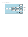
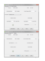
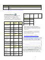
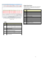
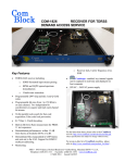
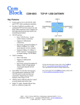
COM-1931 L/S-band burst spread-spectrum transceiver Key Features L/S-band modem to send and receive short UDP frames over wireless, satellite or cable. Direct-Sequence Spread-Spectrum (DSSS) modulation Nominal frequency of operation: 950 – 2175 MHz for direct connection to external LNB or BUC. Customization to other frequency bands is possible. fixed-length 512-bit data frames from/to LAN/UDP ports Multiple frames transmitted efficiently with only 32-symbol separation. Acquisition: 1600-symbol preamble with no apriori knowledge of arrival time o Large frequency acquisition range: ±(chip_rate / 64) or (1.8*symbol_rate), whichever is smaller, with no apriori knowedge. End-to-end latency: 2672 symbol / modulation symbol rate. For example 1.2ms at 2.5Msymbols/s. Programmable chip rate, up to 79.5 Mchips/s 2047-chip Gold codes Data rate: practical range from chip_rate/2047 to chip_rate/30 Frequency reference: internal TCXO or input for an external, higher-stability 10 MHz frequency reference. Built-in tools: PRBS-11 pseudo-random test sequence, BER tester, AWGN generator, internal loopback mode. Monitoring: o Carrier frequency error Burst mode operation: o Supply voltage: 18 – 36VDC with reverse voltage and surge protection. o SNR o BER ComScope –enabled: key internal signals can be captured in real-time and displayed on host computer. For the latest data sheet, please refer to the ComBlock web site: http://www.comblock.com/download/com1931.pdf. These specifications are subject to change without notice. For an up-to-date list of ComBlock modules, please refer to http://www.comblock.com/product_list.html . MSS • 845 Quince Orchard Boulevard Ste N • Gaithersburg, Maryland 20878-1676 • U.S.A. Telephone: (240) 631-1111 Facsimile: (240) 631-1676 www.ComBlock.com © MSS 2015 Issued 8/24/2015 COM-1931 L/S-band burst spread-spectrum modem 80 Mchips/s MSS • 845 Quince Orchard Boulevard Ste N • Gaithersburg, Maryland 20878-1676 • U.S.A. Telephone: (240) 631-1111 Facsimile: (240) 631-1676 www.ComBlock.com © MSS 2015 Issued 8/24/2015 Functional Block Diagram programmable frequency LAN for data and M&C LAN Ethernet MAC UDP/IP Stack Tx RF synthesizer Block mode convolutional FEC encoder Burst DSSS modulator RF quadrature modulator L/S-band RF output Block mode convolutional FEC decoder Burst DSSS demodulator superheterodyne RF receiver L/S-band RF input programmable frequency Rx RF synthesizer 150006 3 Configuration (Basic) The easiest way to configure the COM-1931 is to use the ComBlock Control Center software supplied with the module on CD. Please follow the few simple steps described in the user manual “ccchelp.pdf” document to install the ComBlock Control Center software “ComBlock_Control_Center_windows_rev.exe” Connect the LAN cable between PC and transceiver RJ45 connector labeled “M&C LAN”. Turn the transceiver power supply on and wait approximately 5-10 seconds. In the ComBlock Control Center window, click on the left-most button and select LAN as primary communication media. The default IP address is 172.16.1.128. In the ComBlock Control Center window detect the ComBlock module(s) by clicking the Detect button, next click to highlight the COM-1931 module to be configured, next click the Settings button to display the Settings window shown below. 4 5 Configuration (Advanced) Alternatively, users can access the full set of configuration features by specifying 8-bit control registers as listed below. These control registers can be set manually through the ComBlock Control Center “Advanced” configuration or by software using the ComBlock API (see www.comblock.com/download/M&C_reference.pdf) All control registers are read/write. Definitions for the Control registers and Status registers are provided below. 6 Control Registers The module configuration parameters are stored in volatile (SRT command) or non-volatile memory (SRG command). The stored configuration is automatically loaded up at power up. All control registers are read/write. Note: several multi-byte fields like the IP addresses are enacted upon (re-)writing to the last control register (REG141) Several key parameters are computed on the basis of the 160 MHz ADC clock fclk_adc or the 120 MHz internal processing clock fclk_p. RF Stored frequency f0 Receiver frequency selection Transmitter frequency selection Stored frequency fx Receiver RF Gain Receiver IF Gain Receiver LNA Gain Transmitter ALC target Receiver LNA AGC loop Receiver RF AGC loop Configuration Preselected transmitter or receiver frequency f0. (one of eight stored frequencies) Valid range 925 MHz – 2.175 GHz, expressed in Hz. REG0: bit 7:0 (LSB) REG1: bit 15:8 REG2: bit 23:16 REG3: bit 31:24 (MSB) Use to switch the receiver center frequency among preselected values. Range 0 through 7 REG6(2:0) Use to switch the transmitter center frequency among preselected values. Range 0 through 7 The rx/tx frequencies change is enacted upon writing to REG6. REG6(6:4) Seven additional preselected frequencies x = 1 through 7 Same format as f0. REG(3+4*x): bits 7:0 (LSB) REG(4+4*x): bits 15:8 REG(5+4*x): bits 23:16 REG(6+4*x): bits 31:24 (MSB) Initial RF gain (before the RF AGC takes over). 12-bit. 0 for the minimum gain, 4095 for the maximum gain. The receiver RF gain change is enacted upon writing to REG5. REG4: bits 7:0 (LSB) REG5(3:0): bits 11:8 Initial IF gain (before the IF AGC takes over). 12-bit. 0 for the minimum gain, 4095 for the maximum gain. The receiver IF gain change is enacted upon writing to REG36. REG35: bits 7:0 (LSB) REG36(3:0): bits 11:8 LNA gain 10-bit. 0 for the minimum gain, 1023 for the maximum gain. The receiver IF gain change is enacted upon writing to REG41. REG40: bits 7:0 (LSB) REG41(3:0): bits 11:8 The transmit gain is automatically adjusted so that the measured tx power equals this field. The transmitter gain change is enacted upon writing to REG38. REG37: bits 7:0 (LSB) REG38(3:0): bits 11:8 0 = open loop. LNA path gain is fixed by control registers. 1 = AGC on. Gain is adjusted on the basis of the RSSI measurement. REG39(0) 0 = open loop. RF path gain is fixed by control registers. 1 = AGC on. Out-of-range conditions are detected at the RF mixer and IF power detector. 7 Receiver IFAGC loop Transmitter ON LNB supply LNB supply 13V vs 18V General Parameters REG39(1) 0 = open loop. IF1 path gain is fixed by control registers. 1 = AGC on. Out-of-range conditions are detected at the IF power detector. REG39(3:2) 0 = off 1 = on REG39(6) The transceiver is capable of supplying up to 500mA at 13VDC or 18VDC to an external LNB. This supply voltage is multiplexed with the RF input signal onto the “RF Rx” input. 0 = LNB supply off 1 = LNB supply on REG43(0) 0 = 13VDC LNB supply 1 = 18VDC LNB supply REG43(1) Configuration Internal/External frequency reference 10 MHz output generated from 10 MHz input (-B firmware option) or 19.2 MHz TCXO (-A firmware option) REG46(1): enable(1)/disable(0) CLKREF_OUT (special connector on front-panel) REG46(2): enable(1)/disable(0) CLK_LNB (multiplexed with received signal) REG46(3): enable(1)/disable(0) CLK_TX (multiplexed modulated transmit signal + 10 MHz) FEC encoding K=9 rate ½ convolutional code with zero tail bits. 0 = bypassed 1 = FEC encoding enabled REG47(0) FEC decoding 0 = bypassed 1 = FEC decoding enabled REG47(1) Configuration Modulator Processing clock fclk_tx Modulator processing clock. Also serves as DAC sampling clock. Expressed as as fclk_tx = fclk_p * M / (D * O)) where D is an integer divider in the range 1 - 106 M is a multiplier in the range 2.0 to 64.0 by steps of 1.0. Fixed point format 7.3 O is a divider in the range 2.0 to 128.0 by steps of 1.0. Fixed point format 7.3 Note: the graphical use interface computes the best values for M, D and O. fclk_tx recommended range 80-160 MHz. Chip rate fchip_rate_tx I Code REG48(6:0) = D REG49 = M(7:0) REG50(1:0) = M(9:8) REG51 = O(7:0) REG52(2:0) = O(10:8) The modulator chip rate is in the form fchip_rate_tx = fclk_tx / 2n where n ranges from 1 (2 samples per chip) to 15 (chip rate = fclk_tx / 32768). n is defined in REG53(3:0) Linear feedback shift register initialization. As per [1] REG54 LSB REG55(2:0) MSb 8 Q Code I channel symbol rate fsymbol_rate_i Q channel symbol rate fsymbol_rate_q Output center frequency (fc) REG56 LSB REG57(2:0) MSb The I-channel symbol rate can be set independently of the spreading code period as fsymbol_rate * 232 / fclk_tx REG65 (LSB) – REG62 (MSB) The Q-channel symbol rate can be set independently of the spreading code period as fsymbol_rate * 232 / fclk_tx REG69 (LSB) – REG66 (MSB) The modulated signal center frequency can be shifted in frequency 32-bit signed integer (2’s complement representation) expressed as fc * 232 / fclk_tx Sinusoidal frequency offset REG73 (LSB) – REG70 (MSB) In addition to the fixed frequency offset above, a sinusoidal frequency offset can be generated to mimic Doppler rate in highly mobile applications. This offset is characterized by two parameters: amplitude and period. The amplitude (a frequency) is expressed as fc_amplitude * 232 / fclk_tx in the following control registers: REG74( LSB) – REG77 (MSB) Digital Signal gain Additive White Gaussian Noise gain Input selection Spectrum inversion BPSK / SQPN TX_ENB control The period is expressed as 232 /(fclk_tx *T) in the following control registers: REG78( LSB) – REG81 (MSB) 16-bit amplitude scaling factor for the modulated signal. The maximum level should be adjusted to prevent saturation. The settings may vary slightly with the selected chip rate. Please check for saturation (see test points) when changing either the chip rate or the signal gain. REG82 = LSB REG83 = MSB 16-bit amplitude scaling factor for additive white Gaussian noise. Because of the potential for saturation, please check for saturation (see test points) when changing this parameter. REG84 = LSB REG85 = MSB 0 = from UDP port 1024 1 = internal pseudo-random test sequence. 100ms repetition 2 = internal pseudo-random test sequence continuous transmission 3 = unmodulated test mode (carrier only) REG86(1:0) Invert Q bit 0 = off 1 = on REG86(3) 0 = BPSK 1 = SQPN REG86(4) Future feature. BPSK baseline The TX_ENB signal at the interface controls the RF transmit circuit. During normal operations, 9 the transmitter and ancillary circuits (RF LO) are muted outside of a transmit burst. REG86(5) = 0 However, during tests, the transmitter can be forced to stay ON at all times, for example when the AWGN is generated within. REG86(5) = 1 Demodulator Parameters Tx-Rx loopback Nominal chip rate fchip_rate_rx Configuration REG121(7): enable (1) or disable(0) loopback test mode 32-bit integer expressed as fchip_rate_rx * 232 / fclk_adc. The maximum practical chip rate is fclk_adc /2. The maximum allowed error between transmitted and received chip rate is +/- 100ppm. I Code Q Code Nominal I channel symbol rate fsymbol_rate_i Nominal Q channel symbol rate fsymbol_rate_q I channel spreading factor (Processing gain) Q channel spreading factor (Processing gain) Nominal input center frequency (fc) Spectrum inversion BPSK / SQPN AGC response time REG91 (LSB) – REG94(MSB) Linear feedback shift register A initialization. REG97 LSB REG98(2:0) MSb Linear feedback shift register C REG99 LSB REG100(2:0) MSb Nominal I-channel symbol rate, defined as fsymbol_rate_i * 232 / fclk_adc REG103 (LSB) – REG106 (MSB) Nominal Q-channel symbol rate, defined as fsymbol_rate_q * 232 / fclk_adc REG107 (LSB) – REG110 (MSB) Approximate (i.e rounded) ratio of chip rate / symbol rate Range: 3 – 2047 Note: to effectively achieve this processing gain, the code period must be longer than one symbol duration. REG111 (LSB) REG112(4:0) MSb Approximate (i.e rounded) ratio of chip rate / symbol rate REG113 (LSB) REG114(4:0) MSb The nominal center frequency is a fixed frequency offset applied to the input samples. It is used for fine frequency corrections, for example to correct clock drifts. 32-bit signed integer (2’s complement representation) expressed as fc * 232 / fclk_adc In addition to this fixed value, an optional time-dependent frequency profile can be entered (future). REG115 (LSB) – REG118 (MSB) Invert Q bit 0 = off 1 = on REG119(0) 0 = BPSK 1 = SQPN Future feature. BPSK baseline. REG119(1) Users can to optimize AGC response time while avoiding instabilities (depends on external factors 10 such as gain signal filtering at the RF front-end and chip rate). The AGC_DAC gain control signal is updated as follows 0 = every chip, 1 = every 2 input chips, 2 = every 4 input chips, 3 = every 8 input chips, etc…. 10 = every 1000 input chips. Valid range 0 to 14. REG121(4:0) Network Interface Parameters Configuration LAN MAC REG123. To ensure uniqueness of MAC address. The MAC address most significant bytes are tied to the address LSB FPGA DNA ID. However, since Xilinx cannot guarantee the DNA ID uniqueness, this register can be set at the time of manufacturing to ensure uniqueness. Static IP address 4-byte IPv4 address. Example : 0x AC 10 01 80 designates address 172.16.1.128 REG124: MSB REG125 REG126 REG127: LSB Subnet mask REG128 (MSB) – REG131(LSB) Gateway IP address Destination IP address REG132 (MSB) – REG135(LSB) 4-byte IPv4 address Destination IP address for UDP frames with decoded data. REG136 (MSB) – REG139(LSB) Destination ports I-channel data is routed to this user-defined port number: REG140(LSB) – REG141(MSB) Note: several multi-byte fields like the IP addresses are enacted upon (re-)writing to the last control register (REG141) Monitoring Status Registers Parameters Hardware self-check Power supply check RSSI Monitoring At power-up, the hardware platform performs a quick self check. The result is stored in status registers SREG0-4, SREG16-18 Properly operating hardware will result in the following sequence being displayed: SREG0-SREG4 = 01 F1 1D xx 7F, where xx (bad NAND flash sectors) must be less than 10 SREG16-18 = 0x22 00 87 SREG4(0): PGOOD1 RF1_+3.1V SREG4(1): PGOOD2 IF1+_3.1V SREG4(2): PGOOD3 A_+4.75V SREG4(3): PGOOD4 MOD_+4.8V SREG4(4): PGOOD5 TX_SYNTH_+3.3V SREG4(5): PGOOD6 RX_+4.75V SREG4(6): PGOOD7 RX_SYNTH_+3.3V Overall valid response: 0x7F Received signal strength indicator. 12-bit number Practical range –75 to 0 dBm after LNA and first bandpass filter See RF_POWER_DET1 in schematic. SREG5 = LSB SREG6(3:0) = MSB 11 Received power at RF mixer IF output power Transmit power RF synthesizers locked Power detection at RF mixer. See RF_POWER_DET2 in schematic. SREG7 (LSB) - SREG8(3:0) = MSB Power detection at IF after bandpass filter and IF gain control. See IF1_POWER_DET in schematic. SREG9 (LSB) - SREG10(3:0) = MSB Power detection at the RF transmit output. See TX_POWER_DET in schematic. SREG11 = LSB SREG12(3:0) = MSB ‘1’ when locked SREG19(0): rx synthesizer locked SREG19(1): tx synthesizer locked DSSS demodulator monitoring FEC decoder input BER measurement BER tester synchronized Bit error rate Number of transmitted frames Number of received frames Number of parallel code acquisition circuits Non-coherent integration and dump period N_NCID Measured modulated signal power Measured AWGN power Carrier frequency offset1 Carrier frequency offset2 SNR CIC_R The burst-mode FEC decoder computes the input BER prior to decoding. Mesasured in a frame. This method works with any bit sequence. SREG20 (LSB) - SREG22 (MSB) SREG23(0): 1 when the BERT is synchronized with the received PRBS-11 test sequence. Monitors the BER (number of bit errors over 10,000 received bits) when the modulator is sending a PRBS-11 test sequence. SREG24 (LSB) – 27 (MSB) SREG28 (LSB) – 30 (MSB) SREG31 (LSB) – 33 (MSB) The number of parallel code acquisition circuits is expressed as NACQ = NACQ_DIV * NMUX SREG34: NACQ_DIV SREG35: NMUX SREG36 SREG37(LSB) SREG38 SREG39(MSB) Approximation: noise power is uniform over a range of +/- fclk_tx /2 Therefore, the noise density depends on the selected modulator chip rate (see fclk_tx equation above) SREG40(LSB) SREG41 SREG42(MSB) Residual frequency offset with respect to the nominal carrier frequency (i.e. after frequency profile correction). Part 1/2. 32-bit signed integer expressed as fcerror * * 232 / fclk_p SREG43 (LSB) – SREG46 (MSB) Residual frequency offset with respect to the nominal carrier frequency (i.e. after frequency profile correction). Part 2/2. 32-bit signed integer expressed as fcerror * * 231 / fchip_rate SREG47 (LSB) – SREG50 (MSB) 2*(S+N)/N ratio, valid only during code lock. Linear (not in dBs) Fixed point format 14.2 SREG51 (LSB) – SREG52 (MSB) Receiver decimation factor from fclk_adc to 4* fchip_rate_rx. Valid range 1 - 16384 SREG53 (LSB) – SREG54 (MSB) 12 Network Monitoring Parameters Monitoring LAN PHY ID Expect 0x22 when LAN adapter is plugged in. SREG16 MAC address Unique 48-bit hardware address (802.3). In the form SREG53:SREG54:SREG55:…:SREG58 Multi-byte status variables are latched upon (re-)reading SREG16. ComScope Monitoring Key internal signals can be captured in real-time and displayed on a host computer using the ComScope feature of the ComBlock Control Center. Click on the button to start, then select the signal traces and trigger are defined as follows: Trace 1 signals Format 1: I-channel spread input, directly from ADC (could be at IF) 8-bit signed 2: Demodulated Ichannel 8-bit signed 8-bit unsigned 8-bit signed Format Nominal sampling rate ADC clock fclk_adc Buffer length (samples) 512 512 1: I-channel spread input at near-zero center frequency 8-bit signed 1 sample / I-symbol ADC clock fclk_adc ADC clock fclk_adc Nominal sampling rate ADC clock fclk_adc 2: Code replica. Compare with spread input signals 8-bit signed 2 samples/chip 512 3: last demod AGC gain (I-channel) 4: Symbol tracking phase (accumulated) 8-bit unsigned 8-bit signed Format 1 sample / symbol 1 sample / symbol Nominal sampling rate 2 samples / chip 512 3: FFT magnitude 4: Carrier tracking phase Trace 2 signals Trace 3 signals 1: I-channel after FFT frequency correction, resampling and channel LPF 8-bit signed 2: Demodulated Q-channel 8-bit signed 8-bit signed 3: Code tracking phase correction (accumulated) 1 sample / Q-symbol 2 samples / symbol 4: 2(S+N)/N after despreading. Valid only if code is locked. Linear (i.e. not in dBs) 8-bit unsigned Trigger Signal 1: End of demodulated burst 2: Missed burst detection (at end of expected burst) 3. Demod sync word detection Format Binary Symbol rate / 2.5 512 Binary Binary Signals sampling rates can be changed under software control by adjusting the decimation factor and/or selecting the fclk_adc demod clock as real-time sampling clock. 512 512 Buffer length (samples) 512 In particular, selecting the fclk_adc demod clock as real-time sampling clock allows one to have the same time-scale for all signals. The ComScope user manual is available at www.comblock.com/download/comscope.pdf. 512 Buffer length (samples) 512 512 512 ComScope example, showing trace1 signal2 (in blue): demodulated I-bits during preamble (left) then data (right half). Trace2 signal 4 (in red) shows the I-symbol tracking phase. 13 Digital Test Points The test points are only accessible after opening the enclosure. They are intended to be used only for debugging purposes. ComScope example, showing code lock with aligned: received spread signal after RRC filter (green) vs code replica (red) LEDs LED Power Alarm (red) Tx Rx Sync Tx on Definition Green when power is applied Red when one of these conditions occur: Tx RF frequency synthesizer is out of lock Rx RF frequency synthesizer is out of lock Blink green when a frame from LAN/UDP is being transmitted Blink green when a received frame is forwarded to the LAN/UDP BER tester synchronized (while in test mode. Transmitter must send PRBS11 test sequence) BER tester byte error (valid only if BER tester is synchronized) Test Point Definition J4.1 J4.2 J4.3 J4.4 J4.5 Transmit frame boundaries (0 = idle) Modulator saturation Demod code lock Demod signal presence detected at FFT Demodulator recovered carrier/center frequency (coarse) Demod data field(s) [demod state = 3] Demod sync word detection Missed burst detection FEC decoder input bit error BER tester synchronized BER tester matched filter output (detects start of PRBS11 sequence) Byte error detected by BER tester J4.6 J4.7 J4.8 J4.9 J4.10 J4.11 J4.12 14 Operation Frequency reference Depending on the firmware version loaded, the frequency reference is an external 10 MHz signal supplied through the front panel (-B firmware option) or an internal 19.2 MHz VC-TCXO (-A firmware option). Both -A and –B firmware options are pre-loaded and can be switched easily. Warning: when selected as external frequency reference, the 10 MHz frequency reference must be present prior to powering on the modem. Click on the button below to switch between installed firmware options: Burst format The modulator input consists of a 512-bit fixedlength payload data frame received over LAN/UDP. The payload data frame is encoded with a convolutional code K=9, rate ½, resulting in an encoded frame of length 1040 bits (including the 16 tail bits). Output 10 MHz frequency reference A 10 MHz frequency reference signal can be multiplexed with RF signals on the RF input (to an external LNB) and RF output (to an external BUC). The same 10 MHz is also available as an output on the front panel, labeled “10 MHz OUT”. Each one of these three clocks signals can be enabled or disabled by software command. When transmitting a single frame, the frame is encapsulated in a spread-spectrum burst comprising four distinct fields: no data preamble toggling bits preamble 32-bit synchronization field 1040-bit encoded payload field 512-bit data from UDP port 1040-bit FEC encoded data Spreading codes Each burst undergoes spectrum spreading with userselected pseudo-random codes. All fields (preambles, sync word, data) are spread. Spreading codes are user-selected among a group of 2047-period Gold codes, irrespective of the symbol rate. The codes are selected by their 11-bit A and C registers initialization. 010101 preamble 000000 preamble 32-bit sync 150002 When transmitting multiple frames, follow-on frames are appended without preamble, separated only with a 32-bit sync word. Transmission timing A data frame received over UDP is transmitted without delay. The transmission time uncertainty is small ( < TBD us). The user application is therefore fully in control of the burst scheduling, for example to prevent collisions in a multi-node network. When the modulator is configured in PRBS11 test mode, the PRBS11 pseudo-random test sequence is generated internally, packetized in 512-bit frame 15 and transmitted one frame every 100 ms. The UDP input is ignored while in this mode. Input elastic buffer When more than 512 bits of payload data is needed, multiple data frames can be queued for transmission in the elastic buffer. The modulator expects any follow-on frame to be entirely within the input elastic buffer before the previous frame transmission is complete (so as to avoid transmissing another long preamble). In this case, the modulator only inserts a 32-bit synchronization word between payload frames. The input elastic buffer size is 8Kbit, large enough for 7 encoded frames. symbols for a threshold Eb/N0 of 16 dB (PER > 99.9%). Lower threshold are achievable by increasing the integration time and thus the preamble length, down to Eb/N0 of 5 dB for a preamble length of 32K symbols. Customization has to be specified and quoted at the time of order. Load Software Updates From time to time, ComBlock software updates are released. To manually update the software, highlight the ComBlock and click on the Swiss army knife button. Symbol rate The symbol rate refers to the coded stream. The symbol rate can be set independently of the chip rate and code period. The demodulator includes an autonomous symbol tracking loop, separate from the code tracking loop. The receiver can store multiple personalities. The list of personalities stored within the ComBlock Flash memory will be shown upon clicking on the Swiss army knife button. Frequency acquisition & tracking The frequency acquisition range depends on the chip rate and symbol rate, as defined by ±(chip_rate / 64) or (1.8*symbol_rate), whichever is smaller, with no apriori knowedge. Once locked, the carrier tracking loops tracks the carrier phase over a very wide frequency range. Modulation Baseline: BPSK spread with I-channel code. Possible future extension: SQPN (I and Q channels spread with staggered I and Q code, Q-channel symbol rate = I-channel symbol rate / N, where N is an integer. The default personality loaded at power up or after a reboot is identified by a ‘D’ in the Default column. Any unprotected personality can be updated while the Default personality is running. Select the personality index and click on the “Add/Modify” button. Customization The transceiver design can be customized to meet alternate customer requirements. The customizable features are Custom radio-frequency bands within 400 MHz– 3GHz at no extra charge. Trade-off preamble length versus acquisition threshold Eb/No. The baseline preamble is 1600 16 Interfaces 10/100/1000 Ethernet LAN for data, monitoring and control 10 MHz frequency reference input The software configuration files are named with the .bit extension. The bit file can be downloaded via the Internet, from the ComBlock CD or any other local file. 10 MHz frequency reference output The option and revision for the software currently running within the FPGA are listed at the bottom of the advanced settings window. RF Rx Two firmware options are available for this receiver: -A firmware uses an internal VCTCXO frequency reference. -B firmware option requires an external 10 MHz frequency reference. Recovery The toggle button under the backpanel can be used to (a) prevent the FPGA configuration at power up. This can be useful if a bad FPGA configuration was loaded which resulted in loss of communication with the user. (b) reset the LAN1 IP address to 172.16.1.128. To prevent the FPGA configuration at power up, turn off power. Toggle the button. Turn on power, wait 1 second, then toggle the button a second time. To reset the LAN1 IP address to a factory default of 172.16.1.128: Turn on power. Toggle the button, wait at least 30 seconds, during which time the red led blinks, then toggle the button a second time. Wait another 10 seconds, then cycle power off/on. RF Tx RJ45 Supports auto MDIX to alleviate the need for crossover cable. 10 MHz frequency reference input for frequency synthesis. Sinewave, clipped sinewave or squarewave. SMA female connector Input is AC coupled. Minimum level 0.6Vpp. Maximum level: 3.3Vpp. 10 MHz frequency reference output generated either from the 10 MHz frequency reference input (B firmware option) or from the internal TCXO (-A firmware option) Receiver input. 50 Ohm, SMA female connector. Operating range: -60 to -10 dBm Maximum no damage input level: + 20 dBm Two other signals can be multiplexed onto the same coaxial connection between the COM1931 transceiver and an external LNB: 10 MHz frequency reference (software enabled) Level: -2 dBm typ. 13/18V supply (software enabled) Transmitter output. 50 Ohm, SMA female connector. Transmit level: -30 to 0 dBm, user selectable. One other signal can be multiplexed onto the same coaxial connection between the COM1931 transceiver and an external BUC: 10 MHz frequency reference (software enabled) Level: 0 dBm typ. 17 Operating input voltage range Supply voltage Supply voltage (when no LNB 13/18V supply needed) +18V min, +36V max 400mA typ. under +28VDC +5.6V min, +36V max VHDL code / IP core The FPGA code is written in VHDL. It does not use any third-party software. It occupies the following FPGA resources: The positive voltage is on the center pin, the ground on the outer barrel. Absolute maximum ratings Supply voltage RF input +45 V max +20dBm max Mechanical Interface Aluminum enclosure with rubberized end caps. L x W x H: 168.5mm x 138.96 mm x 40.98 mm. Includes two optional 40mm mounting flanges for mounting to a flat support plate. Schematics The board schematics are available on-line at http://comblock.com/download/com_1900schematics.pdf Configuration Management This specification is to be used in conjunction with VHDL software revision 1 and ComBlock control center revision 3.09q and above. It is possible to read back the option and version of the FPGA configuration currently active. Using the ComBlock Control Center, highlight the COM1931 module, then go to the advanced settings. The option and version are listed at the bottom of the configuration panel. The maximum chip rate is limited by the FPGA technology. For example nearly 80 Mchips/s for Xilinx Artix 7 –1 speed (XC7A100T-1) The IP core, which includes all VHDL source code, can be purchased separately. It is not needed to operate the ready-to-use COM-1931 transceiver. See www.comblock.com/download/com1831soft.pdf Troubleshooting Checklist Demodulator can’t achieve lock even at high signalto-noise ratios: Make sure the modulator baseband I/Q signals do not saturate, as such saturation would strongly distort the modulation phase information. (this is a phase demodulator!) 18 ComBlock Ordering Information COM-1931 L/S-band burst spread-spectrum transceiver ECCN: 5A001.b.3 MSS • 845 Quince Orchard Boulevard Ste N• Gaithersburg, Maryland 20878-1676 • U.S.A. Telephone: (240) 631-1111 Facsimile: (240) 631-1676 E-mail: [email protected] 19