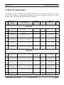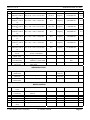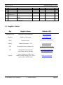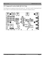
1
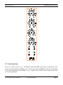
RadioRadio -Flier Electronics RFE-117 EXPONENTIAL VCA USER MANUAL Synopsis: This is the user manual for the RFE-117 VCA for application in a high quality modular analog synthesizer. All technical documentation relating to that product is disclosed herein. The design and all documentation related thereto remain the sole property of Radio-Flier Electronics and is copyrighted material. DOCUMENT CONTROL Revision Number Revision Date Principal Author Assisting Author Document Format Document Status Name of Document Type of Document Storage Location Associated Project Identity 1.0 June 10, 2002 A. Thomas Farrand -noneAuthored in Microsoft Word 2000, distribution via Acrobat PDF First Release RFE117Manual.DOC PERMANENT Author’s PC, 32-bit Drive C:, \My Documents\WORD\SYNTH\ 117VCA This document contains information proprietary to Radio-Flier Electronics, and may not be reproduced, disclosed, or used in whole or in part without the express written consent of RFE. © 2002 Radio-Flier Electronics RFE-117 VCA Modified on June 10, 2002 Table of Contents 1. INTRODUCTION: NOTES FROM THE AUTHOR .............. 3 1.1 1.2 1.3 1.4 1.5 1.6 1.7 Background ................................................................................................................... 4 Usable Product Life .................................................................................................. 4 User Interface ............................................................................................................... 5 Compatibility with Existing Products.............................................................. 6 Performance and Specifications ......................................................................... 6 Physical Characteristics .......................................................................................... 7 Environmental Requirements............................................................................... 7 2. SCHEMATIC DIAGRAM ............................................................................... 7 3. VCA THEORY OF OPERATION............................................................ 8 3.1 3.2 3.3 3.4 3.5 3.6 3.7 Audio Input Mixer Section ................................................................................... 8 Audio Output Buffer Section ............................................................................... 8 VCA Core ...................................................................................................................... 9 Control Voltage Polarity Adjust Section ....................................................... 9 Control Voltage Calibrate Section .................................................................. 10 Temperature Compensation Section............................................................... 10 DC Power Input Section ....................................................................................... 11 4. RFE-117 PARTS LIST ...................................................................................... 12 4.1 Supplier’s Index........................................................................................................ 14 5. ASSEMBLY OF THE VCA .......................................................................... 15 5.1 5.2 5.3 5.4 5.5 5.6 5.7 5.8 5.9 Component Location Guide By Schematic Reference .......................... 15 Component Location Guide By Part Value ................................................ 16 Before You Begin Building The VCA .......................................................... 17 Install The Fixed Resistors .................................................................................. 19 Install The Ceramic Capacitors ......................................................................... 20 Install The Electrolytic Capacitors .................................................................. 20 Install More Stuff ..................................................................................................... 21 Install The Remaining Board-Level Components ................................... 23 Finishing Construction .......................................................................................... 24 6. VCA CALIBRATION ........................................................................................ 25 7. USING THE VCA IN A MODULAR SYSTEM ......................... 27 © 2002 Radio-Flier Electronics A. Thomas Farrand Page 2 RFE-117 VCA Modified on June 10, 2002 1. INTRODUCTION: NOTES FROM THE AUTHOR The RFE-117 VCA was designed to be an inexpensive VCA of high quality. The control-voltage response is exponential and the VCA design is based on an Analog Devices’ SSM2018T VCA core. This VCA core is based on the research of Douglas R. Frey and appears in U.S. patent number 4,471,320, which expired interestingly enough, on September 11, 2001. Yikes! The use of the design documented herein is granted for personal, non-commercial use. I reserve the right to make this design available as a commercial product at any time. As of this writing I have no particular commercial interest but might change my position in the future. I ask that recipients of this document not disseminate this material on the Internet as if it were in the “public domain”. This is not “public domain” information – it is copyrighted by me and produced at no small effort. Thank you for your cooperation! Analog music synthesizers create sound by means of harmonic-rich oscillators and modify that sound through subtractive techniques, using filters and other devices to change the timbre of the sounds produced. One of the most basic elements of sound modification is an electronic volume control, known as a Voltage Controlled Amplifier or simply, VCA. The term VCA is somewhat of a misnomer as most VCAs have very little gain possible. They are more accurately described as a Voltage Controlled Attenuator. In typical use however, there is an expectation of no output signal when the controlling voltage is zero. As the control voltage rises towards a more positive value, the attenuation decreases giving rise to an increase in signal amplitude on the output. Since that “looks” like a voltage-controlled amplifier, the name sticks. The RFE-117 is designed to integrate easily within a contemporary analog synthesizer. Physically the RFE-117 can be fitted onto a “stooge” bracket for mechanical stability and then affixed to a custom “stooge” panel. The custom panel already devised is done in a Synthesis Technology MOTM format for size, appearance, and user interface. The RFE-117 VCA has a 2-input mixer in front of the VCA core. The primary control input is adjustable for differing level inputs and features a polarity changing mechanism. The VCA also features an initial output level adjustment if manual control is desired. © 2002 Radio-Flier Electronics A. Thomas Farrand Page 3 RFE-117 VCA Modified on June 10, 2002 1.1 Background This module was designed as an alternative to some other commercial modules. The availability of such modules from established vendors is not always to my liking, so I rolled my own. While the design of such devices is no simple task, I am willing to put forth the requisite effort and share the results with others. This is probably stupid on my part given the current business climate, but this is a hobby to me and I enjoy it. I would hope that others would do likewise and share their efforts with me. I considered a discrete OTA approach for a VCA, which would have provided simultaneous linear and exponential control. That approach was abandoned as my personal interest was primarily in exponential control. I did not feel like increasing circuit complexity to provide a marginal benefit to me. And with the availability of an excellent exponential control response VCA core from Analog Devices, there was little point in spending gross amounts of time designing, that which already exists. 1.2 Usable Product Life The life of this module should be in excess of 20 years with the components specified. Of course this will be shortened if the unit is subjected to voltages or temperatures beyond design limits. Your mileage may vary, as they say. This module is very simple. There is no “magic” or anything clever about it. It is a very basic VCA with excellent sonic performance. Its simplicity is the key to longevity. © 2002 Radio-Flier Electronics A. Thomas Farrand Page 4 RFE-117 VCA Modified on June 10, 2002 1.3 User Interface There are 4 controls on this VCA. The topmost control knob IN 1 is the input level adjustment for the audio signal input applied to the IN 1 ¼” jack. The second control knob IN 2 is the input level adjustment for the audio signal applied to the IN 2 ¼” jack. Together, these controls form a 2-input mixer for the VCA audio signal input. © 2002 Radio-Flier Electronics A. Thomas Farrand Page 5 RFE-117 VCA Modified on June 10, 2002 The CTRL knob serves two purposes. First, it adjusts the magnitude of the control signal driving the VCA core which is applied via CTRL ¼” jack. Second, it can reverse the polarity of the input control signal to facilitate stereo panning when a pair of RFE-117 VCAs are used at the same time. Alternately, it can be used to normalize the inverted output of envelope generators or LFOs. The INI GAIN knob is a manual “volume” adjustment for the VCA. It sets the initial gain of the VCA when no control signals are present. The effect of this control is summed algebraically with the signal applied to the CTRL ¼” jack, before presentation to the VCA core. 1.4 Compatibility with Existing Products The audio and control inputs are designed for ±5V operation. Excursions somewhat beyond that are tolerated without damage but with possibly unexpected results. Obviously, one cannot apply voltages significantly higher than ±5. ±7V would be about the limit I’d want to shove into the module although the VCA chip itself is rated for ±13V. These voltage limits are very much in keeping with those found on contemporary synthesizers, MOTM in particular. The current consumption of this module is less than 30 ma. per supply rail. 1.5 Performance and Specifications The typical performance of this VCA (according to manufacturer data) is as follows: Supply Voltage Supply Current Dynamic Range Maximum attenuation Control Feedthrough (for a 40 dB gain change) Gain Bandwidth Common Mode Input Range Total Harmonic Distortion Plus Noise @ +10dBu input Total Harmonic Distortion Plus Noise @ other input levels © 2002 Radio-Flier Electronics A. Thomas Farrand ±15V regulated < 30 ma. per rail 117 dB 100 dB ±1 mv 700 kHz ±13V .006% .013% Page 6 RFE-117 VCA Modified on June 10, 2002 1.6 Physical Characteristics The printed circuit board is 5.5” wide by 2.8” deep. The mounting holes line up with a standard fourpotentiometer “stooge” bracket. Potentiometer spacing is MOTM standard of 1.625” between centers. The potentiometer holes are spaced to fit Spectrol or Bourns potentiometers while “poking through” a custom “stooge” panel. There are a number of uncommitted pads that can be used for adding a small custom circuit on this board. There is room for 3, 8-pin chips and passives. ±15V supplies and ground have been brought in close proximity of this “proto area”. I cannot imagine what this are might be used for. It is because I cannot imagine the potential use, that this kludge area exists in the first place. Duh! 1.7 Environmental Requirements The operating temperature should be between 0˚ - 60˚C. Humidity must be kept within the range of 15% 90% non-condensing. (If you can stand to be in the same room with this module for extended periods of time, you will probably not exceed any environmental limit.) 2. SCHEMATIC DIAGRAM The RFE-117 VCA schematic appears as a single sheet, under separate cover. © 2002 Radio-Flier Electronics A. Thomas Farrand Page 7 RFE-117 VCA Modified on June 10, 2002 3. VCA THEORY OF OPERATION The RFE-117 VCA is nothing more than a glorified implementation of the test circuit provided by Analog Devices in the device specification sheet. By implementing the device per manufacturer’s recommendations, one should be able to obtain (nearly) the performance claimed in the specification. I’ve done nothing bizarre with their basic design. Please refer to the schematic diagram when reading the theory of operation for each section. The schematic diagram has section identifiers that coincide with the sections of the theory of operation. The SSM2018T VCA chip has been factory trimmed for minimization of distortion and control voltage feed-through. This simplifies circuit implementation as no trimpots need be added for those functions. The result is a very high quality VCA function that can be implemented at a very low cost. Perhaps discrete designs might beat the specifications of this device, but it is not likely that the cost differential is justified. (That is a statement of opinion, not necessarily fact.) 3.1 Audio Input Mixer Section Referring to the enclosed schematic we start with the audio inputs IN1 and IN2. The audio inputs are summed via R1 and R2 into the inverting input of opamp U2A. R3 sets the gain at unity (in conjunction with R1 and R2 values, of course). While this can be a cause of overload if two signals are mixed at full amplitude, it was necessary to allow for a single input to cause full output amplitude. I strongly recommend the use of the specified OP275 opamp for U2 as that is the device specified in the Analog Devices data sheet for the SSM2018T. Besides, it is pretty much a staple item in synths these days. C7 AC couples the audio signal into the VCA core. The value of C7 primarily determines the lower frequency limit for the VCA. With a value for C7 of 1 microfarad, the low-end response is essentially flat to 14 Hz and down less than 3 decibels at 2Hz. JB1 provides a selection of overall phase of the VCA. The “+” jumper maintains an in-phase relationship between the input and output and is the “normal” configuration. The “-” jumper causes a 180˚ phase difference between the input and output. While of marginal value, this feature was included as it was “free” with this VCA core. (Makes a bullet point on a marketing brochure that is essentially of little to no value.) Still, if this VCA is used to help mangle waveforms in real-time, a 180˚ phase difference could actually prove useful. 3.2 Audio Output Buffer Section The other half of U2 is used to buffer the audio output signal and is set for unity gain. R10 limits output current in a short-circuit situation. (That happens virtually every time one plugs in or removes a patch cord. Its inclusion is common sense.) © 2002 Radio-Flier Electronics A. Thomas Farrand Page 8 RFE-117 VCA Modified on June 10, 2002 3.3 VCA Core The VCA core is comprised of U1 and the passive components connected thereto. The VCA core is connected exactly as prescribed in the device data sheet. The power supply rails are bypassed at the chip by C3 and C4. Capacitor C10 deserves a little explanation. The U1 device has a tendency to increase gain at higher frequencies, which could lead to oscillation. The purpose of C10 is to limit high frequency gain at various VCA gain levels. With the value of C10 shown, U1 is very stable at all frequencies and gain levels. C10 should not be lower than 47 pf nor much more than 200 pf. If one uses too small of a value for C10 the SSM2018T may oscillate at some gain settings. Choosing too large a value for C10 and the high frequency response will suffer. The upper frequency end of this device’s response is essentially flat to beyond 100 kHz with the part values shown. Resistor R11 establishes a class AB operation for the VCA chip. (This part has been optimized for operation for class AB operation.) Typically, distortion in class AB mode is less than 0.05%, which is insignificant in the device application. Obtaining distortion levels lower than this is ludicrous as the signals normally processed are very high in “distortion”. Besides, the distortion level is well below that of a speaker or headphone. Other component values were chosen to match that of the manufacturer’s data sheet as there was no compelling reason to deviate from the suggested values. The data sheet for the SSM2018T can be obtained from the Internet at www.analog.com. Just do a search on SSM2018 and download the PDF data file. You’ll want to retain copy for your records. 3.4 Control Voltage Polarity Adjust Section The control voltage section is pretty straightforward. U3 is configured to provide a normalized or inverted control voltage to the VCA core. U3A functions as a non-inverting buffer for the applied control voltage (at CTRL input). The output voltage is developed across PC3 (CTRL). U3B provides an inverted, unity gain buffer for the applied control voltage. It too develops its output voltage across PC3 (at the opposite end to the output of U3A). The net result is that PC3 can vary the amplitude of the control voltage and the relative polarity. The output of U3 is limited to excursions of ±5V for a ±5V input. © 2002 Radio-Flier Electronics A. Thomas Farrand Page 9 RFE-117 VCA Modified on June 10, 2002 3.5 Control Voltage Calibrate Section U4A provides the requisite voltage inversion for the VCA core and level shifting. This circuit also includes TP1, which is used to calibrate unity gain. The output voltage at pin 1 of U4 ranges from about +4V to –0.5V for normal inputs of 0 to +5V. U4 can be most any dual opamp. Although the schematic shows a Burr-Brown OPA2134 device, a TL072 can be used with the same result. An MXL1013CP would be ideal but the cost may not be justified. If waveform mangling is your bag, use the OPA2134 or the TL072. An MXL1013CP is a precision, but frequency challenged device. (“Frequency challenged”? Aw shit, political correctness is creeping into a mostly technical document. Bogus.) 3.6 Temperature Compensation Section U4B provides the temperature compensation for the VCA. The SSM2018T exhibits a -3500 PPM/˚C temperature drift. This results in a 7 dB change over a temperature range of –40˚C to +85˚C. Personally, I think this is negligible. But if you insist on perfection, make TCR1 a Precision Resistor Company PT146 1K 1% temperature dependant resistor. This is the industry standard part used for negating temperature effects of silicon and is very similar to the devices used on many MOTM modules for temperature compensation. Otherwise, just use a standard 1K ¼ watt 1% resistor for TCR1 and forget about it. (I’m using them because I have a few. If I didn’t have them I wouldn’t buy any.) C12 is used to limit noise introduced by the control input. The result is there is a noticeable lag in control voltages of about 30 milliseconds if one uses slew-limiting values suggested in the data sheet. One can eliminate this lag, with an attending increase in control voltage noise, by eliminating C12 altogether. I would suggest using a 2200 pf capacitor for C12 as a reasonable compromise between reduced control voltage noise and the lag introduced. The choice is up to the builder of the VCA. The control voltage noise is probably more of a spec item issue than something critically important. In a synth, control voltages vary more widely than in a studio-grade mixer (for which the SSM2018T was really designed). As shown on the schematic, the voltage at U1 pin 11 determines VCA gain. With a voltage of +3.5V or greater, the VCA output is effectively shutoff. With a voltage of –0.5V the VCA has an output of greater than +19dBV. If your voltage levels on U1 pin 11 are outside this range, you have probably installed an incorrect part somewhere in the U3/U4 circuit. © 2002 Radio-Flier Electronics A. Thomas Farrand Page 10 RFE-117 VCA Modified on June 10, 2002 3.7 DC Power Input Section The MTA-156 connector (AKA “PEC”) is the standard MOTM-style interface used to bring ±15V and ground to the module. FB1, and FB2 provide a minimum of radio frequency suppression for the power leads. Capacitor C1 and C2 provide localized bypassing for the ±15V supply rails. Unlike MOTM and other manufacturers’ modules, I have selected a low-ESR type of capacitor for C1 and C2. These capacitors are more expensive than others typically used, but are designed to operate at high temperatures for a long period of time. While that isn’t specifically needed here, long life is certainly wanted. That’s the side effect in choosing these specific capacitors. The most likely fault point in this (or most any other) module is the failure of C1 or C2. The electrolyte used in electrolytic capacitors is not a solid; it is more like a gel. Over time and elevated temperatures the electrolyte tends to dry out. The result is that the capacitor is much less efficient and will eventually stop working. When that happens, the module will start to exhibit strange behavior such as oscillating at a high frequency, motor-boating, distorting incoming audio, and so on. By specifying a very high quality capacitor from the outset, one postpones the inevitable failure. © 2002 Radio-Flier Electronics A. Thomas Farrand Page 11 RFE-117 VCA Modified on June 10, 2002 4. RFE-117 PARTS LIST The following is a list of all the parts needed to build the RFE-117 VCA module. Some items were from my junk box and have no corresponding manufacturer (miscellaneous hardware items). All of the important items are listed with full part numbers and suppliers. Qty Manufacturer and Mfgr Part Number Schematic Reference Vendor Vendor Stock Number C1, C2 Digi-Key P10290-ND 0.46 C3-C6, C8, C9, C13, C14 Mouser 581-SR205E104M 0.08 Cap: 1.0 uf 50V radial mono. C7 Digi-Key BC1139CT-ND 0.48 Cap: 82 pf 50V 5% radial mono. C10 Digi-Key BC1012CT-ND 0.12 Cap: 100 pf 50V 5% radial mono. C11 Digi-Key BC1013CT-ND 0.12 Cap: 2200 pf 50V 5% radial mono. C12 Digi-Key BC1074CT-ND 0.11 Res: 100K ¼ watt 1% metal film R1-R3, R7, R8, R14, R15, R20 Digi-Key 100KXBK-ND 0.11 Res: 18.2K ¼ watt 1% metal film R5, R6 Digi-Key 18.2KXBK-ND 0.11 Res: 150K ¼ watt 1% metal film R11 Digi-Key 150KXBK-ND 0.11 Res: 10.0K ¼ watt 1% metal film R12, R21 Digi-Key 10.0KXBK-ND 0.11 Res: 1.00M ¼ watt 1% metal film R13 Digi-Key 1.00MXBK-ND 0.11 Res: 33.2K ¼ watt 1% metal film R4 Digi-Key 33.2KXBK-ND 0.11 Part Description Unit Cost CAPACITORS 2 8 1 1 1 1 Panasonic EEU-FC1V330 AVX SR205E104MAA BC Components K105M20Z5UF5T H5 BC Components K820J15C0GF5TL 2 BC Components K101J15C0GF5TL 2 BC Components K222K15X7RF5T L2 Cap: 33 uf 35V radial electrolytic FC-series Cap: 0.1 uf 50V radial ceramic Z5U 20% RESISTORS 8 2 1 2 1 1 Yageo 100K MF-1/4W-B 1% Yageo 18K2 MF-1/4W-B 1% Yageo 150K MF-1/4W-B 1% Yageo 10K0 MF-1/4W-B 1% Yageo 1M0 MF-1/4W-B 1% Yageo 33K2 MF-1/4W-B © 2002 Radio-Flier Electronics A. Thomas Farrand Page 12 RFE-117 VCA 2 1 2 1 1 1 1 1 1 2 2 1% Yageo 49K9 MF-1/4W-B 1% Yageo 649K MF-1/4W-B 1% Yageo 1K00 MF-1/4W-B 1% Yageo 110K MF-1/4W-B 1% Yageo 332K MF-1/4W-B 1% Yageo 374K MF-1/4W-B 1% Yageo 38K3 MF-1/4W-B 1% Precision Resistor PT146 Bourns 3006P-1-203 Bourns 91A1-B24-D20 Vishay/Spectrol 149-71104 Modified on June 10, 2002 Res: 49.9K ¼ watt 1% metal film R9, R16 Digi-Key 49.9KXBK-ND 0.11 Res: 649K ¼ watt 1% metal film R22 Digi-Key 649KXBK-ND 0.11 Res: 1.00K ¼ watt 1% metal film R10, R24 Digi-Key 1.00KXBK-ND 0.11 Res: 110K ¼ watt 1% metal film R17 Digi-Key 110KXBK-ND 0.11 Res: 332K ¼ watt 1% metal film R18 Digi-Key 332KXBK-ND 0.11 Res: 374K ¼ watt 1% metal film R19 Digi-Key 374KXBK-ND 0.11 Res: 38.3K ¼ watt 1% metal film R23 Digi-Key 38.3KXBK-ND 0.11 Res: 1.00K ¼ watt 1% metal film PT146 +3500 PPM/˚C Trimpot: 20K ¼ watt Cermet TCR1 PRC PT146 1.46 TP1 Digi-Key 3006P-203-ND 1.73 Pot: 100K log taper plastic conductive – panel mount Pot: 100K linear taper Cermet panel mount PC1, PC2 Mouser 5.37 PC3, PC4 Mouser 652-91A1A-B24D20 594-149-7104 IC: SSM2018T VCA U1 SSM2018TP 6.47 IC: OP275 dual opamp U2 OP275GP 2.15 U3, U4 Analog Devices Analog Devices Digi-Key OPA2134PA-ND 2.63 ¼” phone jack with closed circuit J1, J2, J3, J4 Mouser 502-112A 1.44 Ferrite Bead – broadband #43 material MTA-156 power entry connector 8-pin IC socket (optional) Berg connector – 4-pin Shunt jumper 4” length of coaxial audio cable FB1, FB2 Mouser 623-2743002112 0.12 PEC (U2-U4) JB1 (JB1) (J1-J4) Mouser Mouser Mouser Mouser Mouser 571-6404454 571-3902612 649-69192-404 649-68786-202 566-8216-100 0.11 0.08 0.23 0.12 0.18 7.88 SEMICONDUCTORS 1 1 2 Analog Devices SSM2018TP Analog Devices OP275GP Burr-Brown OPA2134PA IC: OPA2134 dual opamp MISCELLANEOUS 4 2 1 3 1 1 4 Switchcraft 112A Fair-Rite 2743002112 Molex Tyco Berg/FCI Berg/FCI Belden 8216 © 2002 Radio-Flier Electronics A. Thomas Farrand Page 13 RFE-117 VCA 4 4 4 4 4 1 Tyco/Alco PKES-90B-1/4 - 1 - Modified on June 10, 2002 #6, ¼” long aluminum spacer 6-32 Philips pan-head screws, ½” 6-32 nut #6 internal tooth lock washer Knob with white pointer stripe - HWS HWS HWS HWS Various - 1.50 Four potentiometer, “short” stooge bracket RFE-117 MOTM-format custom module panel - SPI - - - SPI - - 4.1 Supplier’s Index Key Supplier Name Website URL Analog Devices Analog Devices Incorporated www.analog.com Digi-Key Digi-Key Corporation www.digikey.com HWS Hardware Store (your local Ace or Home Depot!) Mouser Mouser Electronics / TTI www.mouser.com PRC Precision Resistor Company, Inc. www.precisionresistor.com SPI “Stooge Panels Incorporated” (Larry Hendry & Dave Bradley www.wiseguysynth.com www.hotrodmotm.com Various companies sell the Alco knobs at wildly varying prices. Find your best price and stock up! www.tycosucks.com “Various” © 2002 Radio-Flier Electronics A. Thomas Farrand Page 14 RFE-117 VCA Modified on June 10, 2002 5. ASSEMBLY OF THE VCA 5.1 Component Location Guide By Schematic Reference The following is the component location guide by schematic reference. See also the component location guide by part value, which might be a bit more helpful during construction. © 2002 Radio-Flier Electronics A. Thomas Farrand Page 15 RFE-117 VCA Modified on June 10, 2002 5.2 Component Location Guide By Part Value The following is the component location guide by part value. This layout is good for inspecting the board once it is built. See also the other location guide for components by schematic reference. © 2002 Radio-Flier Electronics A. Thomas Farrand Page 16 RFE-117 VCA Modified on June 10, 2002 5.3 Before You Begin Building The VCA You already know how to solder. The choice of solder is up to you. I am probably alone when it comes to solder choice. I prefer 0.020” diameter 2% silver solder with a rosin core (Kester number SN62PB36AG02) and it costs about $28 for a 1-pound spool. Yes, the board must be washed with a strong chemical solvent to remove the flux. No, it does not corrode my solder tips. And no, the board does not have to be washed right away. It can be washed a week after soldering with identical results – no hurry to clean up within an hour’s time. I mention this only in passing and have no desire to start a “solder war”. And yes, all of my MOTM and Oakley modules were assembled using this solder. The RFE-117 VCA does not have a solder mask on either the component or solder side of the board. This makes it easier to create solder-shorts between adjacent traces. To limit solder excursions into unwanted areas, use a small piece of masking tape to cover nearby areas that might inadvertently be soldered. This technique can also be used to prevent the solder from wicking down a trace that is some distance from the donut pad being soldered. As soon as the solder cools, remove the tape to prevent depositing glue goo. Trimming leads on the PC boards is worth a few words. Only those people that are actually reading this paragraph will pickup on this jewel of a tool. Get yourself a pair of Klein D-224-4½C transverse end cutters. I have used many cutting/trimming tools in my day and most of them suck to varying degrees. This tool does not suck. I have been using the same pair I got back in 1974. You’ll love them. I am a big fan of Klein tools. Klein manufactures most of the hand tools I use. I think they are better quality than Xcelite and the cutting edges stay sharp for a very long time. They cost only a bit more than other brands. WARNING! The PC layout is insane from one point of view: the ICs are not inserted uniformly. In fact, every possible orientation is used, save one. Sorry! I am not fond of laying out PC boards. In fact, I hate doing it. Once a placement seems to work for me, that’s where the components stay. But I do think that a ground plane is essential. So rather than wasting time flipping chips around to make it pretty, I spent the extra time to lay down a solder plane that nearly covers the entire component-side of the PC board. Pay attention and you’ll have no problems in that regard. Pin 1 of all ICs employ a square pad instead of a round donut. But do be careful: Once a dual opamp is powered with the chip in backwards, it is toast! Personally, I would socket the opamps only and solder U1 directly onto the PC board. That way, if a “better” opamp is found for this circuit it can be readily swapped in and out for comparison. If you do not like to use sockets then don’t use them. If you use the suggested PT146 temperature dependant resistor for TCR1, it will require the usual silicone heat sink compound like on a VCO. (Place a blob between the backside of TCR1 and the top of U1.) Make certain the heat sink compound is the last thing you apply to the completed VCA. That stuff works great but can make a real mess. Use it sparingly. The printed circuit board is marked COMPONENT SIDE and SOLDER SIDE. The component side of the board has a ground plane that covers a significant portion of the board’s surface. Obviously the components are inserted into the board from the component side and those components are soldered into place from the solder side of the board. I don’t mean to insult anyone’s intelligence, but with adequate © 2002 Radio-Flier Electronics A. Thomas Farrand Page 17 RFE-117 VCA Modified on June 10, 2002 libation I could make that mistake. Hell, with a good Cabernet, normal speech can be reduced to little more than vowel movements. What’s brown and sounds like a bell? Dung. The following assembly guide assumes that you have obtained the requisite components specified in the parts list. If you have made substitutions, your parts may vary slightly from the descriptions given. I will not hold your hand and tell you when it is time to take a break. If you need to pee, go take care of it. Once each component is inserted into the board, it is assumed that you will solder it into place and trim off the excess lead length. Okay, time to get down to brass tacks and build the VCA! © 2002 Radio-Flier Electronics A. Thomas Farrand Page 18 RFE-117 VCA Modified on June 10, 2002 5.4 Install The Fixed Resistors Install the 8, 100K 1% resistors at locations R1, R2, R3, R7, R8, R14, R15, and R20. The color code is: BROWN – BLACK – BLACK – ORANGE – BROWN. Install the 2, 18.2K 1% resistors at locations R5 and R6. The color code for these resistors is: BROWN – GRAY – RED – RED – BROWN. Install the 150K 1% resistor at location R11, next to U1. The color code for resistor R11 is: BROWN – GREEN – BLACK – ORANGE – BROWN. Install the 10.0K 1% resistor at location R12, next to U3. The color code for resistor R12 is: BROWN – BLACK – BLACK – RED – BROWN. Install the 1.0M 1% resistor at location R13, next to R12. The color code for resistor R13 is: BROWN – BLACK – BLACK – YELLOW – BROWN. Install the 33.2K 1% resistor at location R4, next to U2. The color code for resistor R4 is: ORANGE – ORANGE – RED – RED – BROWN. Install the 2, 49.9K 1% resistors at locations R9 and R16. The color code for these resistors is: YELLOW – WHITE – WHITE – RED – BROWN. Install the 649K 1% resistor at location R22, next to U4 (by PC2). The color code for resistor R22 is: BLUE – YELLOW – WHITE – ORANGE – BROWN. Install the 2, 1.00K 1% resistors at locations R10 and R24. The color code for these resistors is: BROWN – BLACK – BLACK – BROWN – BROWN. Install the 110K 1% resistor at location R17, next to U4 (by PC2). The color code for resistor R17 is: BROWN – BROWN – BLACK – ORANGE – BROWN. Install the 332K 1% resistor at location R18, next to U4 (by PC2). The color code for resistor R18 is: ORANGE – ORANGE – RED – ORANGE – BROWN. Install the 374K 1% resistor at location R19, next to U4 (by PC2). The color code for resistor R19 is: ORANGE – VIOLET – YELLOW – ORANGE – BROWN. Install the 17.4K 1% resistor at location R21, L/H side of TP1. The color code for resistor R21 is: BROWN – VIOLET – YELLOW – RED – BROWN. Install the 38.3K 1% resistor at location R23, next to U4. The color code for resistor R23 is: ORANGE – GRAY – ORANGE – RED – BROWN. © 2002 Radio-Flier Electronics A. Thomas Farrand Page 19 RFE-117 VCA Modified on June 10, 2002 Installation of the fixed resistors is now complete. Do not install TCR1 yet! That comes later. 5.5 Install The Ceramic Capacitors Ceramic capacitors have no polarity you need be concerned with but the board is easier to inspect if the component values all face the same way. You are a real synth junkie if choosing between buying your girlfriend a birthday present and another synth module for yourself, is a moral dilemma. Install the 8, 0.1 microfarad ceramic capacitors (marked with 104) at locations C3, C4, C5, C6, C8, C9, C13, and C14. Install the 82 pf ceramic capacitor (marked with 820) at location C10 (next to U1). Install the 100 pf ceramic capacitor (marked with 101) at location C11 (above U1). Install the 2200 pf ceramic capacitor at location C12 (near U4). The 2200 pf capacitor will be labeled 222. Install the 1.0 microfarad ceramic capacitor (marked 105) at location C7. 5.6 Install The Electrolytic Capacitors Electrolytic capacitors have a polarity that must be observed. If installed backwards, they will emit smoke and nasty fumes within seconds of power being applied. Or they may simply explode. (Yes, this is the voice of experience.) Install the 2, 33 microfarad electrolytic capacitors at locations C1 and C2. They are located just above the location for the MTA-156 power connector. The “-” side of the capacitors (with the stripe) are closest to the copyright message imprinted on the component side of the board. The “+” side of C1 and C2 are next to where the ferrite beads will eventually go. If you were expecting more than two electrolytics you are no doubt disappointed as there are only two to be installed. You did pee, right? © 2002 Radio-Flier Electronics A. Thomas Farrand Page 20 RFE-117 VCA Modified on June 10, 2002 5.7 Install More Stuff Install U1, the SSM2018T VCA chip. Please note that this chip has a polarity that must be observed! Pin 1 of the VCA chip must be inserted into the square pad on the printed circuit board for proper orientation. Make certain that all 16 leads protrude through the board before you solder any of the pins. TCR1 will mount on top of this chip, so there is little point in using a socket for U1. Why would you solder in a resistor on top of a socketed component? It can’t come out! Install the dual opamp OP275 at location U2. If you are using a socket, install the socket only at location U2. Please note the orientation for U2 on the component location guide. Please note that this chip has a polarity that must be observed! Pin 1 of U2 must be inserted into the square pad on the printed circuit board for proper orientation. Make certain that all 8 leads protrude through the board before you solder any of the pins. Install the dual opamp OPA2134 at location U3. (You can also use a TL072 instead.) If you are using a socket, install the socket only at location U3. Please note the orientation for U3 on the component location guide. Please note that this chip has a polarity that must be observed! Pin 1 of U3 must be inserted into the square pad on the printed circuit board for proper orientation. Make certain that all 8 leads protrude through the board before you solder any of the pins. Note: pin 1 of both U3 and U2 “point” at each other. (This is part of the wild and crazy layout scheme… be careful!) Install the dual opamp OPA2134 at location U4. (You can also use a TL072 here, too.) If you are using a socket, install the socket only at location U4. Check the orientation for U4 on the component location guide. Please note that this chip has a polarity that must be observed! Pin 1 of U4 must be inserted into the square pad on the printed circuit board for proper orientation. Make certain that all 8 leads protrude through the board before you solder any of the pins. Note: pin 1 of U4 “points” towards U1, the VCA chip. Next, install the two ferrite beads, FB1 and FB2. They are located in close proximity to the electrolytic capacitors just installed. The PC board is fabricated such that the beads, when properly seated, do not come in contact with the component-side foils on the board itself. (There is a rectangular “notch” in the ground plane to accommodate the beads.) Install TP1, the 20K gain calibration trim-pot located to the right of where the MTA-156 power connector will go. As a consequence of lead spacing it will only go in the board the correct way. Next, you’ll install TCR1, the 1K temperature-compensating resistor. If you are using the specified PT146 resistor, bend the leads at a 90˚ right angles about 1 inch apart. The goal is to make that resistor span the length of the U1 chip (the SSM2018) and fit into the appropriate holes. You will notice that I screwed up and made the holes for a PT146 a wee bit too small. If you are using a 1% metal film resistor, the holes are perfect – just plop the resistor on top of U1 and solder away. But if you use a PT146, you’ll need to enlarge the holes slightly to accommodate the larger © 2002 Radio-Flier Electronics A. Thomas Farrand Page 21 RFE-117 VCA Modified on June 10, 2002 diameter wire used on that part. I used a ‘dental pick’ to enlarge the holes a bit and it worked just fine. Don’t get too carried away – they only need to be enlarged very slightly. That seems to be the only boo-boo I made on the board, so you need not search for other documented faults. Install the PEC. That’s the Power Entry Connector and is commonly called an MTA-156 connector. Make certain the connector is soldered into place as shown on the assembly diagram. Install connector JB1. That’s the VCA phase jumper block and consists of 4 square pins on 0.1” centers. Normally the top (+) jumper is used for maintaining a 0˚ phase shift through the VCA. Alternately, one could solder a wire in place of the phase jumpers if you are certain you’d never want to change this setting. © 2002 Radio-Flier Electronics A. Thomas Farrand Page 22 RFE-117 VCA Modified on June 10, 2002 5.8 Install The Remaining Board-Level Components I would suggest that you wash the board at this point and remove the solder flux. It is also a good time to give the board a quick inspection for solder bridges and to make certain the components are in the correct locations and of the proper value. If you are older than 16 years, I suggest you use a magnifying glass to aid this process. Some traces are pretty close. (Well, they look close to this old fart!) Install PC1 and PC2 panel controls. These pots are the 100K audio (log) taper units. They will become the IN 1 and IN 2 level controls. Make certain the pots are flush with the printed circuit board and are aligned flush with the board edge. Remove the mounting hardware and save for later. For now, the hardware just gets in the way. Once you have installed these pots, the board becomes much more fragile. Do exercise care when handling the board once you have begun installing the pots. Install PC3 and PC4 panel controls. These pots are the 100K linear taper, Cermet units. They will become the CTRL and INI GAIN controls. Make certain the pots are flush with the printed circuit board and are aligned flush with the board edge. Remove the mounting hardware and save for later. Prepare 4 lengths of small diameter coaxial cable for connections to the ¼” jacks. Each cable should be about 4” in length. Tin the wires on each end of the coax. Next, solder the outside braid of the coax into the large square pads provided at IN 2, IN 1, OUT, and CTRL as shown on the component location guide. The center conductor of the coax cable goes to the round pads just to the left of the braid connection. (If you have built any MOTM modules, this step should be familiar. If not, you’ll have to use your imagination.) Using 4 cable ties you got from your local hardware store, secure the coax cables to the printed circuit board. There are two holes per coax cable located on the extreme right of the printed circuit board provided for this purpose. (If in doubt, look at the photo on the first page of this document for details related to fastening the coax cables. At this point the board should be essentially complete. Since I don’t use solder with a water-soluble flux, I spot clean the pot and the coax cable connections with my favorite hydrocarbon-based cleaner. For those of you using H2O, do whatever has been working for you so far! If you have included the PT146 temperature-compensating resistor at TCR1, now is the time to spread some of that silicone heat-sink compound between TCR1 and the VCA chip, U1. Use a wooden toothpick to push the compound into place. © 2002 Radio-Flier Electronics A. Thomas Farrand Page 23 RFE-117 VCA Modified on June 10, 2002 5.9 Finishing Construction Using the 4 screws, nuts, lock washers, and ¼” spacers, assemble the board onto the requisite 4-pot stainless-steel “stooge” bracket. Insert the screws from the component-side of the printed circuit board and fit the nuts and lock washers on the blank side of the “stooge” bracket. In all cases, the holes should line up quite well. You may choose other methods for mounting. If you do, just be certain that the mounting holes for the printed circuit board do not short out to anything metal. Attach the completed VCA assembly to the custom black “stooge” panel. Use the saved pot hardware to fit everything together. Fit the knobs onto the pot shafts and tighten. Make certain the alignment of the white line on the knob corresponds appropriately to the legend on the panel. © 2002 Radio-Flier Electronics A. Thomas Farrand Page 24 RFE-117 VCA Modified on June 10, 2002 Attach the 4 Switchcraft ¼” jacks to the “stooge” panel using the supplied hardware. As you face the rear of the VCA assembly, fit the jacks such that the bevel of the jack is in the upper right-hand corner when you tighten the mounting nuts. It will look something like this: Switched Ground "Hot" The OUT jack has only the “hot” (center lead of the coaxial cable) and the ground (braid) connected. The switched contact is left unconnected. On the other 3 jacks, connect the ground (braid) to both the “switched” and “ground” contacts. 6. VCA CALIBRATION Before using the VCA for the first time, ensure there is a jumper for inverting (-) or non-inverting (+) phase through the VCA. If there is no jumper there can be no audio! VCA calibration is simple but is best done with an oscilloscope. Let the VCA warm up at least 2 minutes before calibration. That will ensure the VCA chip is at thermal equilibrium. Use a VCO to inject a standard 5V P-P triangle wave into the IN 1 ¼” jack. Set the IN 1 potentiometer to “10” (maximum clockwise rotation). Set the IN 2 potentiometer to “0” (maximum counter-clockwise rotation). Set the CTRL potentiometer to the centered position (white line straight up). Lastly, set the INI GAIN potentiometer to “10” (maximum clockwise rotation). © 2002 Radio-Flier Electronics A. Thomas Farrand Page 25 RFE-117 VCA Modified on June 10, 2002 Adjust trimpot TP1 such that the output level of the VCA matches the input level. TP1 will allow you to get fairly precise if you’d want. That’s it… you’re done! © 2002 Radio-Flier Electronics A. Thomas Farrand Page 26 RFE-117 VCA Modified on June 10, 2002 7. USING THE VCA IN A MODULAR SYSTEM As a relative newbie to the modular synth world, you probably know better than I how to make use of this module. Note that the CTRL and INI GAIN controls interact a lot. In some configurations they seem a bit too sensitive. In other configurations they’ll seem just right. This VCA works quite differently than the MOTM-110, if that’s your point of reference. You will find this VCA is best at producing natural, percussive sounds. It is quite a bit “perkier” sounding than a linear VCA and that is obvious after playing with it for about two minutes. This VCA does not “replace” linear VCAs. Rather, it is very good at producing some sounds that simply cannot be obtained from a linear VCA. But there are sounds that are better produced by a linear VCA than from this VCA. It all depends on what sort of sound you seek. It is just another tool in the toolbox. One last note: I would be remiss if I did not point out that this VCA is superb in making the limitations of the MOTM-800 ADSR generator quite obvious. Previously, I had said the flaws in the 800 didn’t really bother me all that much. They bother me now. When the control voltage from the 800 misbehaves, it sticks out like a sore thumb. The patch one uses coupled with specific settings of the RFE-117 VCA, makes a big difference in the sound and I was able to become annoyed rather easily. (There is sometimes an extra “bounce” in the VCA output.) When the exponential VCA from Synthesis Technology is eventually released, there will be many more complaints about the 800. Hmmm. Oakley ADSR “guts” behind MOTM-800 panel? That is food for thought. Document End © 2002 Radio-Flier Electronics A. Thomas Farrand Page 27