1
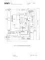
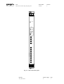
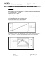
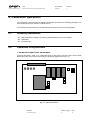
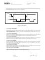
Document type:
User's Manual (MUT)
2.7.
Title:
Mod. V265 8 channel charge integrating ADC
Revision date:
20/04/99
Revision:
0
Integral non linearity test procedure performed by CAEN
PROCEDURE
1.On the V 265 printed-circuit board, set the JP3 jumper to "INT" position: the module's internal
DAC is enabled to supply the CVC inputs with an appropriate signal and an internal GATE signal
can be generated (see 5
Test logic).
2.Set the GATE width to ≈400 ns.
3.By performing a WRITE operation, set the DAC register to an initial voltage value.
4.Read "i" ADC output values (where i = 1 to 50) and calculate the corresponding ηi (medium
value) and σi (standard deviation).
5.Increase the DAC voltage value and repeat the step 4.
6.Repeat step 5 until 50 ηi and σi values are obtained.
7.Calculate the corresponding Best Fit Line (BFL):
8.Calculate the maximum value (Max) of [(BFLi−ηi)+2σi] and the minimum value (Min) of
[(BFLi−ηi)−2σi]where i = 1 to 50. The maximum integral non linearity value is: (Max-Min)/2
Filename:
V265_REV0.DOC
Number of pages:
16
Page:
9