1
Document type:
User's Manual (MUT)
Title:
Mod. V265 8 channel charge integrating ADC
Revision date:
20/04/99
Revision:
0
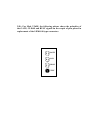
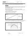
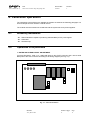
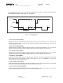
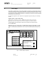
On the piggy-back card, turn the P1 trimmer until a signal which has about the same GATE signal width,
but that switches between 0 and +12/13 Volt, is obtained.
CLEAR
300 ns
GATE
1 µs
1 µs
300 µs
Fig. 4.2 – Timing Diagram
2. U13 OFFSET ADJUSTMENT
Supply the CLR input with a NIM level signal (−800 mV). Connect the voltmeter to U13 - pin 6 and U13
- pin 3. Turn the P1 trimmer located on the printed circuit board until the voltage value shown on the
voltmeter is equal to zero.
3. U22 OFFSET ADJUSTMENT
Supply the CLR input with a NIM level signal (−800 mV). Connect the voltmeter to U22 - pin 6 and to
ground. Turn the P2 trimmer until the voltage value shown on the voltmeter is equal to zero.
4. U1 OFFSET ADJUSTMENT
Supply the CLR input with a NIM level signal (−800 mV). Connect the voltmeter to U1 - pin 6 and to
ground. Turn the P3 trimmer until the voltage value shown on the voltmeter is equal to zero.
5. PEDESTAL ADJUSTMENT
Via Pulse Generator send a 1 µs wide NIM pulse to the GATE connector. Read the ADC1 conversion
value and turn the P4 trimmer until the read value is ≅75. The pedestal is now set to
≈7.5 counts/100 ns (12 bit ADC range).
6. DAC OFFSET ADJUSTMENT
Load the module's DAC with 000H. Connect the voltmeter to U43 - pin 6 and to ground. Turn the R38
trimmer until the voltage value shown on the voltmeter is equal to zero.
7. DAC FULL SCALE ADJUSTMENT
Load the module's DAC with FFFH. Connect the voltmeter to U43 - pin 6 and to ground. Turn the R37
trimmer until the voltage value shown on the voltmeter is equal to -9 V .
Filename:
V265_REV0.DOC
Number of pages:
16
Page:
15