1
Embedded Solutions
20A201S00 E7 – 2010-07-19
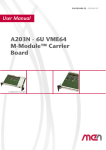
A201S – 6U VMEbus
M-Module™ Carrier Board
Configuration example
User Manual
®
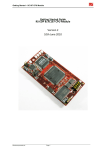
A201S – 6U VMEbus M-Module™ Carrier Board
A201S – 6U VMEbus M-Module™ Carrier Board
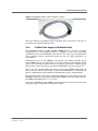
The A201S is an M-Module™ carrier board for universal I/O on the VMEbus,
allowing high flexibility in applications such as process and motion control,
measuring and instrumentation, communication or special-purpose tasks. The
M-Modules™ are screwed tightly on the carrier board, but the board needs only one
slot on the VMEbus. Please note that since all three rows of the P2 connector are
used for user I/O, board models with this connector are not compatible with VME64
backplanes.
An interrupt controller handles the M-Modules™ individually. In VMEbus D16
systems the I/O signals of the M-Modules™ can be accessed from P2/J2 inside the
rack.
MEN Mikro Elektronik GmbH
20A201S00 E7 – 2010-07-19
2
Technical Data
Technical Data
Mezzanine Slots
• Four M-Module™ slots
• Compliant with M-Module™ standard
• Characteristics: D08, D16, A08, INTA, INTC
Interrupt Controller
• Interrupt handling individually for each M-Module™
• Functional compatibility with A201N
Peripheral Connections
• Via front panel
• Via 96-pin P2 connector (rear I/O)
VMEbus
• Only one slot required on the VMEbus
• Models with P2 connector not compatible with VME64 backplanes
(row B of the P2 connector is used for user I/O)
• Slave D08(EO):D16:A16:A24
• Interrupter D08(O)
Electrical Specifications
• Supply voltage/power consumption: +5V (-3%/+5%), 320mA typ. (without
M-Modules™)
Mechanical Specifications
• Dimensions: standard double Eurocard, 233.3mm x 160mm
• Front panel: aluminum with 2 handles, cut-outs for front connectors of 4 M-Modules™
• Weight: 220g
Environmental Specifications
• Temperature range (operation):
- 0..+60°C or -40..+85°C
- Airflow: min. 10m³/h
• Temperature range (storage): -40..+85°C
• Relative humidity range (operation): max. 95% without condensation
• Relative humidity range (storage): max. 95% without condensation
• Altitude: -300m to + 3,000m
• Shock: 15g/11ms
• Bump: 10g/16ms
• Vibration (sinusoidal): 2g/10..150Hz
• Conformal coating on request
MEN Mikro Elektronik GmbH
20A201S00 E7 – 2010-07-19
3
Technical Data
MTBF
• MTBF: 430,000h @ 50°C (derived from MIL-HDBK-217F)
Safety
• PCB manufactured with a flammability rating of 94V-0 by UL recognized manufacturers
EMC
• Tested according to EN 55022 (radio disturbance), IEC1000-4-2 (ESD) and
IEC1000-4-4 (burst)
Software Support
• M-Module™ drivers for Windows®, VxWorks®, Linux, QNX®, OS-9® as supported
MEN Mikro Elektronik GmbH
20A201S00 E7 – 2010-07-19
4
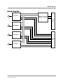
Block Diagram
Block Diagram
F
M-Module
VMEbus Interface/
Interrupt Controller
VMEbus
P1
F
M-Module
F
M-Module
Rear I/O
P2
F
M-Module
MEN Mikro Elektronik GmbH
20A201S00 E7 – 2010-07-19
5
Product Safety
Product Safety
!
Electrostatic Discharge (ESD)
Computer boards and components contain electrostatic sensitive devices.
Electrostatic discharge (ESD) can damage components. To protect the board and
other components against damage from static electricity, you should follow some
precautions whenever you work on your computer.
• Power down and unplug your computer system when working on the inside.
• Hold components by the edges and try not to touch the IC chips, leads, or circuitry.
• Use a grounded wrist strap before handling computer components.
• Place components on a grounded antistatic pad or on the bag that came with the
component whenever the components are separated from the system.
• Store the board only in its original ESD-protected packaging. Retain the original
packaging in case you need to return the board to MEN for repair.
MEN Mikro Elektronik GmbH
20A201S00 E7 – 2010-07-19
6
About this Document
About this Document
This user manual describes the hardware functions of the board, connection of
peripheral devices and integration into a system. It also provides additional
information for special applications and configurations of the board.
The manual does not include detailed information on individual components (data
sheets etc.). A list of literature is given in the appendix.
History
Issue
Comments
Date
E0
First edition
1994-10-21
E1
Second edition (as of hardware rev. 1.x)
1994-11-23
E2
Third edition
1995-11-13
E3
Fourth edition
1998-06-26
E4
Fifth edition
2000-12-18
E5
General update, minor errors corrected
2005-07-22
E6
Added comments about incompatibility with VME64
backplanes
2008-07-24
E7
Clarified description of how to mount M-Modules
2010-07-19
Conventions
!
italics
bold
monospace
hyperlink
This sign marks important notes or warnings concerning proper functionality of the
product described in this document. You should read them in any case.
Folder, file and function names are printed in italics.
Bold type is used for emphasis.
A monospaced font type is used for hexadecimal numbers, listings, C function
descriptions or wherever appropriate. Hexadecimal numbers are preceded by "0x".
Hyperlinks are printed in blue color.
The globe will show you where hyperlinks lead directly to the Internet, so you can
look for the latest information online.
IRQ#
/IRQ
Signal names followed by "#" or preceded by a slash ("/") indicate that this signal is
either active low or that it becomes active at a falling edge.
in/out
Signal directions in signal mnemonics tables generally refer to the corresponding
board or component, "in" meaning "to the board or component", "out" meaning
"coming from it".
Vertical lines on the outer margin signal technical changes to the previous edition of
the document.
MEN Mikro Elektronik GmbH
20A201S00 E7 – 2010-07-19
7
About this Document
Legal Information
MEN Mikro Elektronik reserves the right to make changes without further notice to any products herein. MEN makes no
warranty, representation or guarantee regarding the suitability of its products for any particular purpose, nor does MEN assume
any liability arising out of the application or use of any product or circuit, and specifically disclaims any and all liability,
including without limitation consequential or incidental damages.
"Typical" parameters can and do vary in different applications. All operating parameters, including "Typicals" must be
validated for each customer application by customer's technical experts.
MEN does not convey any license under its patent rights nor the rights of others.
Unless agreed otherwise, MEN products are not designed, intended, or authorized for use as components in systems intended
for surgical implant into the body, or other applications intended to support or sustain life, or for any other application in which
the failure of the MEN product could create a situation where personal injury or death may occur. Should Buyer purchase or
use MEN products for any such unintended or unauthorized application, Buyer shall indemnify and hold MEN and its officers,
employees, subsidiaries, affiliates, and distributors harmless against all claims, costs, damages, and expenses, and reasonable
attorney fees arising out of, directly or indirectly, any claim of personal injury or death associated with such unintended or
unauthorized use, even if such claim alleges that MEN was negligent regarding the design or manufacture of the part.
Unless agreed otherwise, the products of MEN Mikro Elektronik are not suited for use in nuclear reactors and for application
in medical appliances used for therapeutical purposes. Application of MEN products in such plants is only possible after the
user has precisely specified the operation environment and after MEN Mikro Elektronik has consequently adapted and
released the product.
ESM™, ESMini™, MDIS™, MDIS4™, MDIS5™, MENMON™, M-Module™, M-Modules™, SA-Adapter™, SAAdapters™, UBox™, USM™ and the MBIOS logo are trademarks of MEN Mikro Elektronik GmbH. PC-MIP® is a
registered trademark of MEN Micro, Inc. and SBS Technologies, Inc. MEN Mikro Elektronik®, ESMexpress®, MIPIOS®
and the MEN logo are registered trademarks of MEN Mikro Elektronik GmbH.
Microsoft® and Windows® are registered trademarks of Microsoft Corp. Windows® Vista™ is a trademark of Microsoft
Corp.OS-9®, OS-9000® and SoftStax® are registered trademarks of RadiSys Microware Communications Software Division,
Inc. FasTrak™ and Hawk™ are trademarks of RadiSys Microware Communications Software Division, Inc. RadiSys® is a
registered trademark of RadiSys Corporation. QNX® is a registered trademark of QNX Ltd. Tornado® and VxWorks® are
registered trademarks of Wind River Systems, Inc.
All other products or services mentioned in this publication are identified by the trademarks, service marks, or product names
as designated by the companies who market those products. The trademarks and registered trademarks are held by the
companies producing them. Inquiries concerning such trademarks should be made directly to those companies. All other brand
or product names are trademarks or registered trademarks of their respective holders.
Information in this document has been carefully checked and is believed to be accurate as of the date of publication; however,
no responsibility is assumed for inaccuracies. MEN Mikro Elektronik accepts no liability for consequential or incidental
damages arising from the use of its products and reserves the right to make changes on the products herein without notice to
improve reliability, function or design. MEN Mikro Elektronik does not assume any liability arising out of the application or
use of the products described in this document.
Copyright © 2010 MEN Mikro Elektronik GmbH. All rights reserved.
Please recycle
Germany
MEN Mikro Elektronik GmbH
Neuwieder Straße 5-7
90411 Nuremberg
Phone +49-911-99 33 5-0
Fax +49-911-99 33 5-901
E-mail [email protected]
www.men.de
MEN Mikro Elektronik GmbH
20A201S00 E7 – 2010-07-19
France
MEN Mikro Elektronik SA
18, rue René Cassin
ZA de la Châtelaine
74240 Gaillard
Phone +33 (0) 450-955-312
Fax +33 (0) 450-955-211
E-mail [email protected]
www.men-france.fr
USA
MEN Micro, Inc.
24 North Main Street
Ambler, PA 19002
Phone (215) 542-9575
Fax (215) 542-9577
E-mail [email protected]
www.menmicro.com
8
Contents
Contents
1 Getting Started . . . . . . . . . . . . . . . . . . . . . . . . . . . . . . . . . . . . . . . . . . . . . . . .
1.1 Map of the Board. . . . . . . . . . . . . . . . . . . . . . . . . . . . . . . . . . . . . . . . .
1.2 Integrating the Board into a System . . . . . . . . . . . . . . . . . . . . . . . . . .
1.3 Installing M-Modules . . . . . . . . . . . . . . . . . . . . . . . . . . . . . . . . . . . . .
1.4 Installing Driver Software . . . . . . . . . . . . . . . . . . . . . . . . . . . . . . . . . .
11
11
12
13
13
2 Address Organization . . . . . . . . . . . . . . . . . . . . . . . . . . . . . . . . . . . . . . . . . . . 14
3 Functional Description . . . . . . . . . . . . . . . . . . . . . . . . . . . . . . . . . . . . . . . . . .
3.1 Power Supply. . . . . . . . . . . . . . . . . . . . . . . . . . . . . . . . . . . . . . . . . . . .
3.2 VMEbus Interface . . . . . . . . . . . . . . . . . . . . . . . . . . . . . . . . . . . . . . . .
3.2.1
Slave Interface. . . . . . . . . . . . . . . . . . . . . . . . . . . . . . . . . . . .
3.2.2
Interrupter . . . . . . . . . . . . . . . . . . . . . . . . . . . . . . . . . . . . . . .
3.2.3
VMEbus Connector P1 . . . . . . . . . . . . . . . . . . . . . . . . . . . . .
3.3 M-Module Interfaces . . . . . . . . . . . . . . . . . . . . . . . . . . . . . . . . . . . . . .
3.3.1
M-Module Connectors . . . . . . . . . . . . . . . . . . . . . . . . . . . . .
3.3.2
Connecting Peripherals to P2 . . . . . . . . . . . . . . . . . . . . . . . .
3.3.3
16-MHz Clock Supply of M-Module Slots. . . . . . . . . . . . . .
3.4 Interrupt Controller . . . . . . . . . . . . . . . . . . . . . . . . . . . . . . . . . . . . . . .
3.4.1
Registers of the Controller . . . . . . . . . . . . . . . . . . . . . . . . . .
3.4.2
Power-Up/Reset Behavior. . . . . . . . . . . . . . . . . . . . . . . . . . .
15
15
15
15
17
17
19
19
20
22
23
23
24
4 Appendix . . . . . . . . . . . . . . . . . . . . . . . . . . . . . . . . . . . . . . . . . . . . . . . . . . . . . 25
4.1 Literature and Web Resources . . . . . . . . . . . . . . . . . . . . . . . . . . . . . . . 25
4.2 Finding out the Board’s Article Number, Revision and Serial Number25
MEN Mikro Elektronik GmbH
20A201S00 E7 – 2010-07-19
9
Figures
Figure 1.
Figure 2.
Figure 3.
Figure 4.
Figure 5.
Figure 6.
Figure 7.
Figure 8.
Map of the board — top view. . . . . . . . . . . . . . . . . . . . . . . . . . . . . . . .
Installing an M-Module . . . . . . . . . . . . . . . . . . . . . . . . . . . . . . . . . . . .
Setting the base address — Default (A24) . . . . . . . . . . . . . . . . . . . . . .
Setting the base address — Example (A16) . . . . . . . . . . . . . . . . . . . . .
Connection of 21-pin cables to P2 . . . . . . . . . . . . . . . . . . . . . . . . . . . .
Locking hook and coding keys of 21-pin receptacle . . . . . . . . . . . . . .
M-Module cable, 21-pin receptacle - pig tail . . . . . . . . . . . . . . . . . . . .
Labels giving the board’s article number, revision and serial number.
11
13
16
16
21
21
22
25
Address organization . . . . . . . . . . . . . . . . . . . . . . . . . . . . . . . . . . . . . .
Address modifier codes permitted on A201S. . . . . . . . . . . . . . . . . . . .
Pin assignment of the 96-pin VMEbus P1 connector. . . . . . . . . . . . . .
Pin Assignment of the 40-Pin M-Module connector . . . . . . . . . . . . . .
Correspondence between 96-pin connector and 21-pin connectors . . .
14
17
18
19
20
Tables
Table 1.
Table 2.
Table 3.
Table 4.
Table 5.
MEN Mikro Elektronik GmbH
20A201S00 E7 – 2010-07-19
10
Getting Started
1
Getting Started
This chapter will give an overview of the carrier board and some hints for first
installation in a system as a "check list".
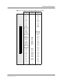
1.1
Map of the Board
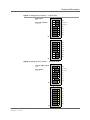
Figure 1. Map of the board — top view
M-Module 3
VMEbus
Backplane
P1
I/O
Connector
I/O
Connector
M-Module 2
S2
DIL Switches for Setting
the Base Address
S1
MEN Mikro Elektronik GmbH
20A201S00 E7 – 2010-07-19
M-Module 0
96-pin receptacle
I/O
Connector
96-pin shroud
M-Module 1
P2
I/O
Connector
4
M-Module 3
3
M-Module 2
2
M-Module 1
1
M-Module 0
11
Getting Started
1.2
Integrating the Board into a System
You can use the following hints and "check list" to install the carrier board into a
VMEbus system for the first time and to test proper functioning of the board.
!
The A201S has an A24/D16 or A16/D16 VMEbus slave interface. This interface
only requires the board's upper 96-pin connector (P1) on the board. With the
standard version of the board, the lower connector (P2) can be used for connecting
peripherals. In this case row B of the connector is also used, making the board
incompatible with VME64 backplanes. If you use a 32-bit VMEbus system, you
need to leave out the lower bus (P2) of the A201S VME slot. If this is not possible,
you can use an alternative model of the A201S instead. This model does not have a
P2 connector - which, of course, means that peripherals can only be connected via
the front panel.
If it is required for the board to issue an interrupt via the bus, then the daisy chain
must be established through to the A201S.
!
The carrier board is completely trimmed on delivery. Perform the following
procedure without an M-Module installed!
; Power-down the system.
; The board is set for A24 accesses, the base address being 0xE00000. This
base address is set using DIL switches. It may be necessary to set it to an
address with which the master can access the board in A24/D16 mode.
(If you have to change the base address, please refer to Chapter 3.2.1.1 Setting
the Base Address on page 15.)
; Insert the A201S into your VMEbus system, making sure that the VMEbus
connectors are properly aligned.
; Power-up the system.
; After power-up, load a suitable debugger.
; First, attempt to perform a read-word access to the base address plus 0x100,
(i.e. 0xE00100 if the base address was not altered).
With 32-bit masters it may be necessary to load a register on the master board
to set the access mode. In any case you should be aware of the contents of the
high-order byte of the 32-bit address. For instance, access may require using
address 0xFFE00100 or 0xFCE00100 or any other address (depends on the
master board).
; If a bus error occurs while you are attempting to read, check if the base address
is set correctly and whether it is possible for the master to access the VMEbus
at all at the selected address and using the correct mode. Then try again.
; Now attempt to perform a word access to the base address plus 0x102. Again,
no bus error should occur. Write accesses to this memory location should be
successful for the right half of the word. For instance, if 0x55 is written to the
register it should be possible to read 0xxx55.
; You must have completed this test successfully before you begin to integrate an
M-Module into the system (see Chapter 1.3 Installing M-Modules on page 13
and description in the respective M-Module user manual).
Note: Interrupts cannot be tested in this simple fashion.
MEN Mikro Elektronik GmbH
20A201S00 E7 – 2010-07-19
12
Getting Started
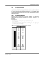
1.3
Installing M-Modules
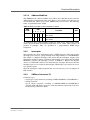
Perform the following steps to install an M-Module:
; Hold the M-Module over the target slot of the A201S with the component sides
facing each other.
; Put the M-Module’s front connector through the front panel slot, holding the
M-Module at a 45° angle.
; Align the 24-pin and 40-pin connectors of the M-Module and carrier board.
; Press the M-Module carefully but firmly on the A201S, making sure that the
connectors are properly linked. Don’t press the boards together by force,
because this may lead to bending of the M-Module PCB! A part of the carrier
board connector may remain visible. Make sure that the PCBs are in parallel, as
shown in the figure below.
; Turn the A201S upside down and use four M-Module mounting screws to fasten the M-Module on the solder side of the A201S.
Note: You can order suitable mounting screws from MEN. For ordering information, see MEN’s website.
Figure 2. Installing an M-Module
M-Module
Mounting Bolt
24-pin connector
40-pin connector
A201S
Don’t press the boards together by force, because this
may lead to bending of the M-Module PCB!
A part of the carrier board connector may remain visible.
M-Module
The PCBs must be in parallel.
A201S
M3x6 cross-recess
countersink-head
screw (DIN 965)
1.4
M3x6 slotted panhead screw
(plastics) (DIN 85)
Installing Driver Software
For a detailed description on how to install driver software please refer to the
respective documentation.
You can find any driver software available for download on MEN’s website.
MEN Mikro Elektronik GmbH
20A201S00 E7 – 2010-07-19
13
Address Organization
2
Address Organization
The A201S occupies an address space of 0x800 bytes on the VMEbus. These
0x800 bytes are divided into 4 identical parts. Each 0x200-byte part is assigned to
one M-Module slot. 0x100 bytes are used for addressing the M-Module itself. The
remaining 0x100 bytes for each M-Module slot are used to address a part of the
interrupt controller.
This means that each M-Module on the A201S has the same address mapping. This
greatly facilitates writing software since it is only necessary to take into account the
base address of the M-Module, and not the base address of the carrier board as well.
Each M-Module has its own interrupt vector register and its own control register.
The 0x100 bytes for each M-Module used to address the interrupt controller are
not fully coded. The two registers of the interrupt controller are replicated several
times in this address space. Whether the M-Module actually codes the whole of the
0x100 bytes or not depends on the M-Module concerned.
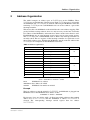
Table 1. Address organization
Offset Address
Function
0x000..0x0FF
M-Module
0x101
Control Register
0x103
Vector Register
0x200..0x2FF
M-Module
0x301
Control Register
0x303
Vector Register
0x400..0x4FF
M-Module
0x501
Control Register
0x503
Vector Register
0x600..0x6FF
M-Module
0x701
Control Register
0x703
Vector Register
M-Module
0
1
2
3
The base address base of an M-Module is calculated by the formula
base = A201Sbase + modslot ⋅ 0x200
base
M-Module base address
A201Sbase base address of A201S
modslot
M-Module slot number on A201S
Example
The base address set for the A201S is 0xE00000. An M-Module is plugged into
M-Module slot 2. The M-Module base address is then
0xE00000 + 2 ⋅ 0x200 = 0xE00400
For instance, if we are dealing with a 32-bit master which addresses the standard
address area at 0xFFxxxxxx, then the M-Module at address 0xFFE00200 is
selected. The corresponding interrupt control register then has address
0xFFE00301.
MEN Mikro Elektronik GmbH
20A201S00 E7 – 2010-07-19
14
Functional Description
3
Functional Description
3.1
Power Supply
The 5V power supply from the VMEbus is sufficient for the carrier board. Some
M-Modules (e.g. serial interfaces) need ±12V as well.
3.2
VMEbus Interface
3.2.1
Slave Interface
The A201S board is equipped with an A16/A24/D16 slave interface, i.e, only cycles
with standard (24-bit) addresses and short (16-bit) address range are supported. For
accesses from the VMEbus, the slave recognizes this type of cycle on the basis of
the address modifier lines. The data bus interface of the A201S complies with the
D16 specification. However, some M-Modules with a data bus width of only 8 bits
permit only D08(O) accesses. The slave recognizes this type of access by the state
of lines DS0*, DS1*, LWORD* and A1. The A201S will operate with masters
which support so-called "address pipelining". The access time on the A201S
depends on the M-Module concerned. DTACK* is generated 120ns after AS* at the
earliest. The maximum time is limited to 10µs - in line with the M-Module
Standard.
3.2.1.1
Setting the Base Address
The A201S occupies an area of 0x800 in the address space. Identical quarters of
this - that is 0x200 - are reserved for each M-Module together with the interrupt
handler.
The base address of the A201S can be varied in increments of 0x800 within the
whole A16 or A24 address range. It is set using DIL switches, which remain
accessible after the M-Modules are fit. There is one switch for each address bit from
A11 to A23. If the switch is "on", the corresponding address bit is compared with 0.
If the switch is "off", it is compared with 1. If the address is the same as the switch
setting (taking address modifiers into account), a "select" signal for the board is
generated. In the short address range, the switches corresponding to A16 to A23 are
ignored.
The selection between short address range and standard address range is made by
the SRT switch. If SRT is switched on, short accesses are possible; if SRT is
switched off, standard accesses are allowed.
MEN Mikro Elektronik GmbH
20A201S00 E7 – 2010-07-19
15
Functional Description
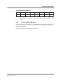
Figure 3. Setting the base address — Default (A24)
Default Mode
A24
off
on
Default Base Address
0xE00000
S2
S1
1
0
off
on
1
1
SRT
2
Not used
3
Not used
4
A11
5
A12
6
A13
7
A14
8
A15
1
A16
2
A17
3
A18
4
A19
5
A20
6
A21
7
A22
8
A23
1
SRT
2
Not used
3
Not used
4
A11
5
A12
6
A13
7
A14
8
A15
1
A16
2
A17
3
A18
4
A19
5
A20
6
A21
7
A22
8
A23
0
Figure 4. Setting the base address — Example (A16)
Example Address Mode
A16
off
on
Base Address
0x4000
S2
S1
MEN Mikro Elektronik GmbH
20A201S00 E7 – 2010-07-19
1
0
off
on
1
0
16
Functional Description
3.2.1.2
Address Modifiers
The VMEbus has 6 "address modifier" lines. These lines allow the master to transfer
additional binary information to the slave during a data transfer cycle. The lines are
used to divide the address space of the VMEbus into several classes. The following
codes are permitted for the A201S:
Table 2. Address modifier codes permitted on A201S
HEX
Code
AM
5
4
Function
SRT
3
1
0
3d, 39
H H H
L
H Standard supervisory and non-privileged
data access
off
2d, 29
H
L
H Short supervisory and non-privileged
data access
on
L
H
As mentioned above, SRT specifies standard or short access. The factory setting
allows supervisor-mode and nonprivileged-mode access. Other address modes are
possible in principle. They are specified in a programmable FLEX Logic
component.
3.2.2
Interrupter
The interrupter has been implemented using a FLEX Logic IC. This chip permits
interrupts to be issued at a programmable level independently for each M-Module.
The A201S is a D08(O) interrupter. This means that the interrupter outputs status
information on D0..D7 during an interrupt acknowledge cycle. Depending on which
M-Module generates the interrupt it can be an RORA (= Release On Register
Access) or an ROAK (= Release On Acknowledge) interrupt. This means that the
interrupt request is reset either by the interrupt acknowledge cycle itself or by access
to a specific register.
Since the interrupter is fully programmable, it is not necessary to set any jumpers or
DIL switches.
3.2.3
VMEbus Connector P1
Connector types:
• 96-pin type-C plug connector according to DIN41612/MIL-C-55302/IEC603-2
• mating connector:
type-C 96-pin receptacle according to DIN41612/MIL-C-55302/IEC603-2,
available with solder/wire-wrap pins, for hand-soldering connection or for insulation piercing connection (IDC)
MEN Mikro Elektronik GmbH
20A201S00 E7 – 2010-07-19
17
Functional Description
Table 3. Pin assignment of the 96-pin VMEbus P1 connector
ABC
1
32
MEN Mikro Elektronik GmbH
20A201S00 E7 – 2010-07-19
A
B
C
D0
-
D8
D1
-
D9
D2
-
D10
D3
-
D11
D4
-
D12
D5
-
D13
D6
-
D14
D7
-
D15
GND
-
GND
SYSCLK
-
-
GND
-
-
/DS1
-
/SYSRST
/DS0
-
/LWORD
/WRITE
-
AM5
GND
-
A23
/DTACK
AM0
A22
GND
AM1
A21
/AS
AM2
A20
GND
AM3
A19
/IACK
GND
A18
/IACKIN
-
A17
/IACKOUT
-
A16
AM4
GND
A15
A7
/IRQ7
A14
A6
/IRQ6
A13
A5
/IRQ5
A12
A4
/IRQ4
A11
A3
/IRQ3
A10
A2
/IRQ2
A9
A1
/IRQ1
A8
-12V
-
+12V
+5V
+5V
+5V
18
Functional Description
3.3
M-Module Interfaces
A total of four M-Modules can be installed on the A201S. Peripheral equipment
may be connected at the front using the M-Module’s front connector or at the rear
using the carrier board’s second DIN 41612 connector (P2). In 32-bit systems, either
the system's lower bus printed circuit board must be cut away here or the A201S
must be ordered without P2. In the latter case, of course, the peripherals can only be
connected at the front.
3.3.1
M-Module Connectors
The signals from the carrier board are fed to the M-Module via a 40-pin plug
connector. This plug connector corresponds to a receptacle connector on the
M-Module.
Connector types:
• Two 20-pin plugs, 2.54mm pitch, square pins ∅ 0.635mm gold
• Mating connector:
Two 20-pin receptacles, high-precision, 2.54mm pitch, for square pins
∅ 0.635mm gold, 6.9mm height
Table 4. Pin Assignment of the 40-Pin M-Module connector
A B
1
20
MEN Mikro Elektronik GmbH
20A201S00 E7 – 2010-07-19
A
B
/CS
GND
A01
+5V
A02
+12V
A03
-12V
A04
GND
A05
-
A06
-
A07
GND12V
D08
D00
D09
D01
D10
D02
D11
D03
D12
D04
D13
D05
D14
D06
D15
D07
DS1
DS0
/DTACK
/WRITE
/IACK
/IRQ
/RESET
SYSCLK
19
Functional Description
3.3.2
Connecting Peripherals to P2
Normally peripheral signals are fed to M-Modules via the front panel connector
(e. g. 25-pin D-Sub). However, many M-Modules offer the alternative to connect
peripheral signals via the carrier board. In this case the signals are connected to the
board’s 96-pin P2 connector using 21-pin receptacles and fed to the M-Module
through its 24-pin receptacle (see MEN’s website for ordering information).
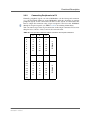
You can connect up to four 21-pin connectors to the 96-pin connector. Please note
that pins 8a,b,c; 16a,b,c; 24a,b,c and 32a,b,c cannot be used.
B
A
1
3
2
1
2
6
5
4
3
9
8
7
4
12
11
10
5
15
14
13
6
18
17
16
7
21
20
19
8
-
-
-
...
...
...
...
25
3
2
1
26
6
5
4
27
9
8
7
28
12
11
10
29
15
14
13
30
18
17
16
31
21
20
19
32
-
-
-
MEN Mikro Elektronik GmbH
20A201S00 E7 – 2010-07-19
...
M-Module 0
C
M-Module 3
Table 5. Correspondence between 96-pin connector and 21-pin connectors
20
Functional Description
96-pin receptacle
96-pin shroud
P2
Figure 5. Connection of 21-pin cables to P2
4
M-Module 3
3
M-Module 2
2
M-Module 1
1
M-Module 0
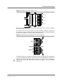
The 21-pin receptacle has a locking hook matching the 96-pin receptacle and thus
preventing wrong connection:
On its other side, the 21-pin receptacle has four removable coding keys. Make sure
to remove the respective coding key before linking the 21-pin connector and the 96pin receptacle. Otherwise you may damage the connectors!
Figure 6. Locking hook and coding keys of 21-pin receptacle
locking
hook
1
2
removable
coding keys
3
4
Assembled cables are available for connection to the P2 connector. The components
used are from AMP. The wiring connections for the 21-pin M-Module connector are
crimped. The cable is 2m long and has a pig tail, i.e. you can choose whichever
connector you need on the other side of the cable. See MEN’s website for ordering
information.
MEN Mikro Elektronik GmbH
20A201S00 E7 – 2010-07-19
21
Functional Description
Figure 7. M-Module cable, 21-pin receptacle - pig tail
The color coding for assignment of the individual wires of the cable to the pins of
the connector is supplied with the cable.
3.3.3
16-MHz Clock Supply of M-Module Slots
Some M-Modules make use of the 16-MHz VMEbus clock as a time base. A couple
of applications use this 16-MHz clock in a VMEbus system as the centralized
synchronous timer for all M-Modules. For instance, this is the case for multichannel
data acquisition systems, which must make sure that all sample procedures are
synchronized.
Unfortunately there are also VMEbus systems that cause trouble with this signal.
Some VMEbus system slot components (e.g. older components from Tundra) do not
generate the clock signal when a reset occurs. Other systems have such bad signal
quality that on some slots proper operation of M-Modules cannot be guaranteed.
This is why the standard models of A201S generate the 16-MHz clock locally. If
you use several A201S boards within a system, the M-Modules on each board will
operate synchronously, but the different A201S boards operate asynchronously.
For applications that need strictly synchronized operation of the entire system, the
M-Module clock can also be generated from the VMEbus clock. For models that use
the VMEbus SYSCLK please contact MEN.
If you use SYSCLK from the VMEbus, you should make sure that clock generation
and signal quality correspond to standardized values.
MEN Mikro Elektronik GmbH
20A201S00 E7 – 2010-07-19
22
Functional Description
3.4
Interrupt Controller
The FLEX Logic chip handles local interrupt sources with the VMEbus. It supports
all signals used for the VMEbus interrupt protocol. Interrupt vectors from the local
source of the interrupt can be passed on, and the chip also provides the capability of
passing a pre-programmed vector. Eight internal registers (four status registers and
four vector registers) are provided for general use.
3.4.1
Registers of the Controller
The interrupt controller contains eight programmable read-write registers. The four
control registers control the activity of the chip, the other four are the vector
registers, which contain the vector information for the IACK cycle. One pair of
registers is allocated to the M-Module.
Control Registers (read/write)
X/IN
IRE
IRAC
L
MEN Mikro Elektronik GmbH
20A201S00 E7 – 2010-07-19
7..6
5
4
3
-
X/IN
IRE
IRAC
2
1
0
L
External/internal
This bit governs behavior during an IACK cycle. If the X/IN bit is 0, the
chip replies with the /DTACK signal and the vector stored in its vector
register, i.e. it replies internally. If the X/IN bit is set, the M-Module has to
generate the vector and the /DTACK signal.
0=
Reply internally
1=
Reply externally
Interrupt enable
This bit must be 1 to allow an interrupt to be generated at all. If this bit is 0,
no interrupt is triggered on the VMEbus—even though an interrupt from
the M-Module is pending.
0=
Disable
1=
Enable
Interrupt auto clear
If this bit is 1, the IRE bit is cleared during an IACK cycle (in response to
this interrupt request) which disables the interrupt. In order to enable the
interrupt again, the IRE bit must be set again by writing to the Control
Register.
Interrupt level
These bits select the line on which the interrupt request is to be generated.
0 0 0 = Disable interrupt generation
0 0 1 = Generate interrupt request on line /IRQ1
0 1 0 = Generate interrupt request on line /IRQ2
0 1 1 = Generate interrupt request on line /IRQ3
1 0 0 = Generate interrupt request on line /IRQ4
1 0 1 = Generate interrupt request on line /IRQ5
1 1 0 = Generate interrupt request on line /IRQ6
1 1 1 = Generate interrupt request on line /IRQ7
23
Functional Description
Vector Registers (read/write)
7
6
5
4
3
2
1
0
V7
V6
V5
V4
V3
V2
V1
V0
V7..V0
3.4.2
interrupt vectors
If the X/IN bit is ’0’, this vector is generated at D0..D7 during the IACK
cycle.
Power-Up/Reset Behavior
At power-up, the control registers are all loaded with 0x00, the vector registers are
set to the value 0x0F. This value corresponds to the 68000 vector for an
uninitialized interrupt.
After a reset only the interrupt level is set to zero.
MEN Mikro Elektronik GmbH
20A201S00 E7 – 2010-07-19
24
Appendix
4
Appendix
4.1
Literature and Web Resources
• A201S data sheet with up-to-date information and documentation:
www.men.de
• M-Module Standard:
ANSI/VITA 12-1996, M-Module Specification;
VMEbus International Trade Association
www.vita.com
4.2
Finding out the Board’s Article Number, Revision and
Serial Number
MEN user documentation may describe several different models and/or hardware
revisions of the A201S. You can find information on the article number, the board
revision and the serial number on two labels attached to the board.
• Article number: Gives the board’s family and model. This is also MEN’s ordering number. To be complete it must have 9 characters.
• Revision number: Gives the hardware revision of the board.
• Serial number: Unique identification assigned during production.
If you need support, you should communicate these numbers to MEN.
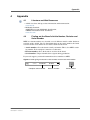
Figure 8. Labels giving the board’s article number, revision and serial number
Made in
Germany
Article No.:
01A201S00
Complete article number
MEN Mikro Elektronik GmbH
20A201S00 E7 – 2010-07-19
Rev.No.:
00.00.00
Revision number
Serial number
25