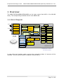
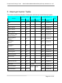
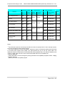
1
FUJITSU SEMICONDUCTOR
MB91F467BA/466BA/465BA/464BA
preliminary datasheet
MB91460 series
European MCU Design Centre (EMDC)
Fujitsu Microelectronics Europe GmbH
Pittlerstr. 47
63225 Langen, Germany
Fujitsu and
Fujitsu Microelectronics Solutions Limited(FMSL)
Version 0.27, File: mb91f467ba_shortspec_r2.0.doc
European MCU Design Centre
MB91F467BA/466BA/465BA/464BA preliminary datasheet ver. 0.27
Revision History
Version
0.10
0.11
0.12
0.13
Date
2005-09-01
2005-09-04
2006-01-20
2006-01-25
0.14
2006-02-14
0.15
2006-02-16
0.16
0.17
0.18
2006-03-08
2006-03-09
2006-06-08
0.19
2006-07-20
0.20
2006-07-25
2006-08-07
0.21
0.22
2006-08-08
2007-03-12
2007-04-09
Remark
Initial draft
Memory map + flash memory map updated
Addition of external bus interface option
Corrections for external bus interface option;
Remove of package information: MB91F467BA will be delivered
in a QFP-144 package with pure Sn pin plating, the related
package number is to be defined
Use UART3 instead of UART2
Upgrade tables and feature lists to refer to external bus interface
option
Updated pinning, added 1 USART in non-external-bus mode,
exchanged WRX[1] against WRX[0]
Changed pinning for 6ch CAN, 32ch ADC and NMI
Corrected operation supply voltage range
Delete “ESD Protection” of Electrical Characteristics
Added condition of current consumption
Add a postscript to “function limitation” in “2.1.Overview Table”
Add the “6. IO Map”
1.1.Block Diagram change IO Voltage
2.2.1.Memory Map change “not available area”
2.2.7.&2.2.8. correct memory capacity.
2.3. correct feature of “Clock supervisor”
6. Add a postscript to “function limitation”
Add a Cancellation line “D/A Converter”,”Interrupt Control Unit”
and “CAN 0-5 Status Flags”
4. Added “Type” in Table
6. Del a Cancellation line ”Interrupt Control Unit”
Add a Cancellation line Test function
(C-Unit Test, “CSVCR(bit7)”,”CANCKD”and”I-Unit Test)
6. Del a postscript(*4) It was already descripted “User’s Manual”.
Added MB91F465BA information
“A Cover” & 1 & 4.1 & 4.2.1 & 4.2.2 Add “MB91F465BA”
1.1 & 2.1 Add 544KB FLASH and explanation of FLASH
2.2.1
Add memory map of MB91F465BA
2.2.9
Add 544KB Fash memory map
6
Add Flash area of MB91F465BA
Changed a discription about Clock supervisor
2.3 Clock supervisor function revival
Added “4.3 I/O Pin Types”
Page 2 of 125
European MCU Design Centre
0.23
2007-04-12
2007-04-19
2007-05-01
0.24
2007-05-30
0.25
2007-06-18
0.26
2007-07-24
MB91F467BA/466BA/465BA/464BA preliminary datasheet ver. 0.27
Added MB91F466BA/MB91F464BA information
“A Cover” & 1 & 4.1 & 4.2.1 & 4.2.2
Add “MB91F466BA” and”MB91F464BA
1.1 & 2.1 Add 832KB/416KB FLASH and explanation of FLASH
2.2.1
Add memory map of MB91F466BA/MB91F464BA
2.2.9
Add 832KB/416KB Fash memory map
6
Add Flash area of MB91F466BA/MB91F464BA
Change of Chapter Constitution and Addition of “Recommended
Settings”
Chap1 Overview
(no change)
Chap2 Feature List
(small change in this Chap)
Chap3 Recommended Settings
(addition)
Chap4 IO Map
(Chap6 in a previous Ver.)
Chap5 Interrupt Vector Table
(Chap3 in a previous Ver.)
Chap6 Package and Pin Assignment (Chap4 in a previous Ver.)
Chap7 Electrical Characteristics
(Chap5 in a previous Ver.)
Addition of information to be related Flash
(From 2.4.1 to 2.4.4)
Added information of specification change about port function.
2.2.7 & 6.2.2 Add “Limitation”
2.2.7
Add “WRX1”
6.2.2
Change function of Pin44.
Changed a division point of IO power supply group
6.2.1 & 6.2.2
Added package dimension in “6.1 Package”
Change of initial value in “4 IO map”
LVSEL (04C4h) : 00000111 -> 00000101
REGSEL(04CEh) : 00000110 -> 00000100
Changed of initial value in “4 IO map”
PFR00 (0D80h) : 00000000 -> 11111111
PFR01 (0D80h) : 00000000 -> 11111111
PFR02* (0D80h) : 00000000 -> 11111111
PFR03* (0D80h) : 00000000 -> 11111111
PFR04* (0D84h) : 00000000 -> 11111111
PFR05 (0D84h) : . . 000000 -> . . 111111
PFR06 (0D84h) : 00000000 -> 11111111
PFR07 (0D84h) : 00000000 -> 11111111
PFR08 (0D88h) : 0 . .0 . . .0 -> 1 . .1 . . .1
PFR09 (0D88h) : . . . . . . 00 -> . . . . . . 11
PFR10 (0D88h) : . . . . . . . 0 -> . . . . . . . 1
* PFR02, PFR03, and PFR04 changed only the description.
Because it is a part that IO doesn't have.
0.27
2007-09-05
# 2.1 :Changed “Core” and “Resource” frequency.
・Core frequency 80 MHz / 100 MHz -> 96 MHz
・Resource frequency 40 MHz / 50 MHz -> 48 MHz
# 2.2.2:Changed maximum operating frequency and PLL clock
multiplier method.
・Core clock = “80 MHz /100 MHz” -> “96 MHz”
・multiplied by 20 -> multiplied by 24
Page 3 of 125
European MCU Design Centre
0.27
MB91F467BA/466BA/465BA/464BA preliminary datasheet ver. 0.27
# 3.3 :The combination description of “CMPR : 03E9” ,
“Baseclk : 52MHz” and “Fmax : 96.9MHz” was deleted
from the table.
# 7.2 :Parameter item in table :
The maximum frequency was changed from 100MHz to
96MHz about the frequency description of “Lock-up time
PLL1”.
Latest revision
Page 4 of 125
European MCU Design Centre
MB91F467BA/466BA/465BA/464BA preliminary datasheet ver. 0.27
Table of contents
1
Overview........................................................................................................................ 7
1.1
2
Block Diagram .......................................................................................................... 7
Feature List ................................................................................................................... 8
2.1
Overview Table......................................................................................................... 8
2.2
Core Functionality................................................................................................... 10
2.2.1
Memory Map .................................................................................................... 11
2.2.2
FR70 CPU Core............................................................................................... 13
2.2.3
Instruction Cache ............................................................................................. 13
2.2.4
Interrupt Controller ........................................................................................... 14
2.2.5
Internal Data RAM............................................................................................ 14
2.2.6
Internal Program/Data RAM ............................................................................. 14
2.2.7
External Bus Interface...................................................................................... 14
2.2.8
DMA Controller................................................................................................. 15
2.3
Peripheral Function ................................................................................................ 16
2.4
Embedded Program/Data Memory ......................................................................... 21
2.4.1
Flash features .................................................................................................. 21
2.4.2
CPU Mode ....................................................................................................... 22
2.4.2.1
Flash configuration in CPU mode .......................................................................................... 22
2.4.2.2
Flash access timing settings in CPU mode ............................................................................ 24
2.4.2.3
Address mapping from CPU to parallel programming mode.................................................... 25
2.4.3
2.4.3.1
Flash configuration in parallel flash programming mode ......................................................... 26
2.4.3.2
Pin connections in parallel programming mode ...................................................................... 27
2.4.4
3
Parallel flash programming mode..................................................................... 26
Flash Security .................................................................................................. 28
2.4.4.1
Vector addresses.................................................................................................................. 28
2.4.4.2
Security Vector FSV1............................................................................................................ 28
2.4.4.3
Security Vector FSV2............................................................................................................ 31
2.4.4.4
Register description for Flash Security................................................................................... 32
Recommended Settings ............................................................................................. 33
3.1
PLL and Clockgear settings.................................................................................... 33
3.2
Flash interface settings........................................................................................... 34
3.3
Clock Modulator settings ........................................................................................ 35
4
IO Map.......................................................................................................................... 39
5
Interrupt Vector Table................................................................................................101
Page 5 of 125
European MCU Design Centre
6
Package and Pin Assignment ...................................................................................109
6.1
Package ................................................................................................................109
6.2
I/O Pins and their functions....................................................................................111
6.2.1
MB91F467BA / 466BA / 465BA / 464BA with MD_3 = 0..................................111
6.2.2
MB91F467BA / 466BA / 465BA / 464BA with MD_3 = 1..................................116
6.3
7
MB91F467BA/466BA/465BA/464BA preliminary datasheet ver. 0.27
I/O Pin Types.........................................................................................................121
Electrical Characteristics ..........................................................................................126
7.1
Absolute Maximum Ratings ...................................................................................126
7.2
Operating Conditions.............................................................................................127
7.3
Converter Characteristics ......................................................................................129
Page 6 of 125
European MCU Design Centre
MB91F467BA/466BA/465BA/464BA preliminary datasheet ver. 0.27
1 Overview
The MB91F467BA/466BA/465BA/464BA are the body control flash MCU of the M91460
family. The corresponding evaluation device is the MB91V460.
1.1 Block Diagram
4MHz
Clock
Clock modulation
modulation
Clock
Clock Control
Control
Clock
Clock Supervisor
Supervisor
32 KHz
FRT
FRT xx 88
Int.
Int. Control
Control
Power Control
Subclock
Subclock 32
32 kHz
kHz
EDSU/MPU
EDSU/MPU
FR 70 CPU
FR70 CPU
0.0.
1818um
um
100
100MHz
MHz
Watchdog
Watchdog
Bit
Bit Search
Search
RC
RC Osc.
Osc. 100
100 kHz
kHz
RAM
RAM 24KB
24KB
Core: 1.8V
IO: 3.3-5.0V
QFP144
QFP144
Pre-fetch
Pre -fetch 8KB
FLASH
FLASH
467BA
1088 KB
1088: KB
466BA : 832 KB
465BA : 544 KB
464BA : 416KB
RAM16KB
16KB
RAM
BootROM4KB
4KB
BootROM
ICU
ICU xx 88 (4)
(4)
OCU
OCU xx 88 (4)
(4)
PPG
P PG xx 16
16 (8)
(8)
2
I2ICCxx22
R-timer
R
-Timer xx 88
(4)
LIN-UART
LIN
- UART xx77(4)
GPIO
GPIO
CAN x 6
CAN x 6
32 msg
32 msg
RTC
RTC
(12)
Ext.Int
16 (12)
Ext.
Int xx 16
U/DCnt x 2 (0)
U/DCnt x 2(0)
NMI
NMI xx 11
Alarm
Alarm xx 11
10bit ADC
ADC x 32
10Bit
(16) (16)
INSDAT DATA
INSTR
TR
HarvardBus
Bus
Harvard
Converter
Converter
Ext.
I/FI/F
Option
Ext.
Option
16-bit
data
16-bit
data
DMA
DMA(5(5ch)
ch)
4 LIN-USART + FIFO
(x) Resources in case of
bus interface option
In case of the bus interface option only the blue coloured numbers of resources will be
available. The bus interface option is enabled via the pin MD_3.
Page 7 of 125
European MCU Design Centre
MB91F467BA/466BA/465BA/464BA preliminary datasheet ver. 0.27
2 Feature List
2.1 Overview Table
Feature
MB91V460
MB91F467BA / 466BA / 465BA / 464BA
MD_3 = 0
MD_3=1
Core frequency
80 MHz
96 MHz
Resource frequency
40 MHz
48 MHz
Watchdog
yes
yes
Bit Search
yes
yes
Reset Input
yes
yes
Clock Modulator
(yes)
yes
DMA
5 ch
5 ch
MPU/EDSU
16 ch
8 ch
1024 KB + 64 KB (MB91F467BA)
Flash
external
768 KB + 64 KB (MB91F466BA)
512 KB + 32 KB (MB91F465BA)
384 KB + 32 KB (MB91F464BA)
Flash Protection
n.a.
yes
D-bus RAM
64 KB
24 KB
GP RAM
64 KB
16 KB
Direct mapped cache
16 KB
8 KB
Boot-ROM
4 kB
4 KB
RTC
1 ch
1 ch
Free Running Timer
8 ch
8 ch *2
ICU
8 ch
8 ch
4 ch *3
OCU
8 ch
8 ch
4 ch *7
Reload Timer
8 ch
PPG
16 ch
PFM
1 ch
-
Sound Generator
1 ch
1 ch
8 ch *4
8 ch *5
16 ch
Page 8 of 125
European MCU Design Centre
Feature
UpDown Counter
C_CAN
MB91F467BA/466BA/465BA/464BA preliminary datasheet ver. 0.27
MB91V460
MB91F467BA / 466BA / 465BA / 464BA
4 ch
6 ch (128 msg buffer)
LIN-USART
16 ch (4 ch FIFO)
I2C
MD_3 = 0
MD_3=1
2 ch
- *8
6 ch x 32 msg buffer
7 ch (4 ch FIFO) *1
4 ch
4 ch (4 ch FIFO)
2 ch
32-bit address / 32-bit
data
-
22-bit address /
16-bit data
External Interrupts
16 ch
16 ch
12 ch *6
NMI
1 ch
1 ch
SMC
6 ch
-
LCD
1 ch 40x4
-
FR external bus
ADC (10-bit)
32 ch
Alarm Comparator
2 ch
1 ch
Low voltage detection
yes
yes
Clock Supervisor
yes
yes
BGA 660
LQFP-144
Package
32 ch
16 ch
*1(LIN) : USART CH0(shared with external bus) can be used for asynchronous mode only.
*2(FRT) : MD3=0 → CH1&0 can’t select ext. clock(bit7 of TCCS1,0)
MD3=1 → CH3,2,1&0 can’t select ext. clock(bit7 of TCCS3,2,1,0)
*3 (ICU): MD3=1 → Don’t set PFR = 1 & EPFR = 1 (for LIN Synch Field detect)
because there is not CH3-0 of LIN-USART.
*4 (RLT): MD3=1 → CH7,6,5&4 can’t select ext. event
*5 (PPG): MD3=1 → You can use CH15-8 of PPG. CH15-12 can’t select ext. trigger.
*6 (Ext-INT): INT7-4(shared with external bus) can be used for MD3=0 mode only.
*7 (OCU): MD3=1 → You can’t use ext.out-port.(but, OCU-function is active.)
*8 (UDC): MD3=1 → You can use Timer-mode only.
Page 9 of 125
European MCU Design Centre
MB91F467BA/466BA/465BA/464BA preliminary datasheet ver. 0.27
2.2 Core Functionality
Page 10 of 125
European MCU Design Centre
MB91F467BA/466BA/465BA/464BA preliminary datasheet ver. 0.27
2.2.1 Memory Map
MB91F467BA
0000:0000h-
0000:00FFh
0000:0100h-
I/O Halfword Data
0000:0100h-
I/O Word Data
0000:0200h-
0000:1000h-
I/O
0000:0400h-
0000:0100h-
DMA
0000:1000h-
I/O Word Data
0000:0200h-
I/O Word Data
0000:03FFh
I/O
0000:0400h-
I/O
0000:0FFFh
DMA
0000:1000h-
0000:10FFh
available, but no
memory mapped
access
I/O Halfword Data
0000:01FFh
0000:0FFFh
0000:10FFh
0000:2000h-
I/O Halfword Data
0000:03FFh
0000:0FFFh
I/O Byte Data
0000:00FFh
0000:01FFh
0000:03FFh
0000:0400h-
0000:0000h-
0000:00FFh
0000:01FFh
0000:0200h-
MB91F466BA
I/O Byte Data
DMA
0000:10FFh
0000:2000h-
Flash Memory I-Cache (8 kB)or
0000:2000h-
Flash Memory I-Cache (8 kB)or
0000:5FFFh
Instruction RAM (8 kB)
0000:5FFFh
Instruction RAM (8 kB)
Flash Memory Control
0000:7000h-
Flash Memory Control
0000:7000h-
Flash Memory Control
0000:70FFh
Flash Memory I-Cache Control
0000:70FFh
Flash Memory I-Cache Control
0000:70FFh
Flash Memory I-Cache Control
0000:8000h-
Boot ROM (4 kB)
0000:8000h-
Boot ROM (4 kB)
0000:8000h-
Boot ROM (4 kB)
0000:5FFFh
Flash Memory I-Cache (16 kB) or
Instruction RAM (16 kB)
0000:7000h-
0000:BFFFh
0000:C000h-
0000:BFFFh
CAN
0000:C000h-
0000:CFFFh
0000:BFFFh
CAN
0000:C000h-
0000:CFFFh
CAN
0000:CFFFh
0001:0000h-
External Bus I-Cache (4 kB) or
0001:0000h-
External Bus I-Cache (4 kB) or
0001:0000h-
External Bus I-Cache (4 kB) or
0001:FFFFh
Instruction RAM (4 kB)
0001:FFFFh
Instruction RAM (4 kB)
0001:FFFFh
Instruction RAM (4 kB)
0002:0000h-
Data RAM (64 kB)
0002:0000h-
Data RAM (24 kB)
0002:0000h-
Data RAM (24 kB)
0002:FFFFh
0003:0000h-
0002:FFFFh
Instruction/Data RAM (64 kB)
0003:0000h-
0003:FFFFh
0002:FFFFh
Instruction/Data RAM (16 kB)
0003:0000h-
0003:FFFFh
0003:FFFFh
ROMS00
0004:0000h-
0004:0000h-
0005:FFFFh
(128 kB)
0005:FFFFh
0005:FFFFh
0006:0000h-
ROMS01
0006:0000h-
0006:0000h-
0007:FFFFh
(128 kB)
0007:FFFFh
0008:0000h-
ROMS02
0008:0000h-
Flash Memory Area
0009:FFFFh
(128 kB)
0009:FFFFh
(1024 kB + 64 kB)
000A:0000h-
ROMS03
000A:0000h-
000B:FFFFh
(128 kB)
000B:FFFFh
000C:0000h-
ROMS04
000C:0000h-
000D:FFFFh
(128 kB)
000D:FFFFh
External Bus Area
000E:0000h-
ROMS05
000E:0000h-
depending on ROMA
setting
000F:FFFFh
or
ROMS0-7 setting fixed to internal area
0004:0000h-
0007:FFFFh
0008:0000h-
Flash Memory Area
0009:FFFFh
(768 kB + 64 kB)
000A:0000h000B:FFFFh
000D:FFFFh
External Bus Area
000E:0000h-
depending on ROMA
000F:FFFFh
setting
(128 kB)
000F:FFFFh
Emulation SRAM Area
ROMS06
0010:0000h-
0013:FFFFh
(max 4.864 kB)
(256 kB)
0013:FFFFh
ROMS07
0014:0000h-
0014:0000h-
(256 kB)
0017:FFFFh
0017:FFFFh
ROMS08
0018:0000h-
0018:0000h-
0017:FFFFh
or
0018:0000h-
64 kB
0010:0000h0013:FFFFh
External Bus Area
(256 kB)
001B:FFFFh
001B:FFFFh
001C:0000h-
depending on ROMA/ROMS
ROMS09
001C:0000h-
001C:0000h-
001F:FFFFh
setting
(256 kB)
001F:FFFFh
0020:0000h-
ROMS10
0020:0000h-
0027:FFFFh
(512 kB)
0027:FFFFh
0028:0000h-
ROMS11
0028:0000h-
002F:FFFFh
(512 kB)
002F:FFFFh
0030:0000h-
ROMS12
0030:0000h-
0037:FFFFh
(512 kB)
0037:FFFFh
0038:0000h-
ROMS13
0038:0000h-
003F:FFFFh
(512 kB)
003F:FFFFh
0040:0000h-
ROMS14
0040:0000h-
0047:FFFFh
(512 kB)
0047:FFFFh
0048:0000h-
ROMS15
0048:0000h-
004F:FFFFh
(512 kB)
004F:FFFFh
0050:0000h-
External Bus Area
FFFF:FFFFh
Legend
0050:0000hFFFF:FFFFh
ROMS8-15 setting fixed to external area
001B:FFFFh
External Bus Area
or
000C:0000h-
0010:0000h0014:0000h-
Instruction/Data RAM (16 kB)
64 kB
001F:FFFFh
0020:0000h0027:FFFFh
0028:0000h002F:FFFFh
0030:0000h-
External Bus Area
0037:FFFFh
0038:0000h003F:FFFFh
0040:0000h0047:FFFFh
0048:0000h004F:FFFFh
External Bus Area
0050:0000h-
External Bus Area
FFFF:FFFFh
Memory available in this area
Memory not available in this area
Page 11 of 125
ROMS0-7 setting fixed to internal area
I/O Byte Data
ROMS8-15 setting fixed to external area
MB91V460A
0000:0000h-
MB91F467BA/466BA/465BA/464BA preliminary datasheet ver. 0.27
MB91F465BA
I/O Byte Data
0000:0000h-
0000:00FFh
0000:0100h-
I/O Halfword Data
0000:0100h-
I/O Word Data
0000:0200h-
0000:1000h-
I/O
0000:0400h-
0000:0100h-
DMA
0000:1000h-
I/O Word Data
0000:0200h-
I/O Word Data
0000:03FFh
I/O
0000:0400h-
I/O
0000:0FFFh
DMA
0000:1000h-
0000:10FFh
available, but no
memory mapped
access
I/O Halfword Data
0000:01FFh
0000:0FFFh
0000:10FFh
0000:2000h-
I/O Halfword Data
0000:03FFh
0000:0FFFh
I/O Byte Data
0000:00FFh
0000:01FFh
0000:03FFh
0000:0400h-
0000:0000h-
0000:00FFh
0000:01FFh
0000:0200h-
MB91F464BA
I/O Byte Data
DMA
0000:10FFh
0000:2000h-
Flash Memory I-Cache (8 kB)or
0000:2000h-
Flash Memory I-Cache (8 kB)or
0000:5FFFh
Instruction RAM (8 kB)
0000:5FFFh
Instruction RAM (8 kB)
Flash Memory Control
0000:7000h-
Flash Memory Control
0000:7000h-
Flash Memory Control
0000:70FFh
Flash Memory I-Cache Control
0000:70FFh
Flash Memory I-Cache Control
0000:70FFh
Flash Memory I-Cache Control
0000:8000h-
Boot ROM (4 kB)
0000:8000h-
Boot ROM (4 kB)
0000:8000h-
Boot ROM (4 kB)
0000:5FFFh
Flash Memory I-Cache (16 kB) or
Instruction RAM (16 kB)
0000:7000h-
0000:BFFFh
0000:C000h-
0000:BFFFh
CAN
0000:C000h-
0000:CFFFh
0000:BFFFh
CAN
0000:C000h-
0000:CFFFh
CAN
0000:CFFFh
0001:0000h-
External Bus I-Cache (4 kB) or
0001:0000h-
External Bus I-Cache (4 kB) or
0001:0000h-
External Bus I-Cache (4 kB) or
0001:FFFFh
Instruction RAM (4 kB)
0001:FFFFh
Instruction RAM (4 kB)
0001:FFFFh
Instruction RAM (4 kB)
0002:0000h-
Data RAM (64 kB)
0002:0000h-
Data RAM (24 kB)
0002:0000h-
Data RAM (24 kB)
0002:FFFFh
0003:0000h-
0002:FFFFh
Instruction/Data RAM (64 kB)
0003:0000h-
0003:FFFFh
0002:FFFFh
Instruction/Data RAM (16 kB)
0003:0000h-
0003:FFFFh
0003:FFFFh
ROMS00
0004:0000h-
0004:0000h-
0005:FFFFh
(128 kB)
0005:FFFFh
0005:FFFFh
0006:0000h-
ROMS01
0006:0000h-
0006:0000h-
0007:FFFFh
(128 kB)
0007:FFFFh
0008:0000h-
ROMS02
0008:0000h-
0009:FFFFh
(128 kB)
0009:FFFFh
Flash Memory Area
000A:0000h-
ROMS03
000A:0000h-
(512 kB + 32 kB)
000B:FFFFh
(128 kB)
000B:FFFFh
or
000C:0000h-
ROMS04
000C:0000h-
External Bus Area
000D:FFFFh
(128 kB)
000D:FFFFh
depending on ROMA
000E:0000h-
ROMS05
000E:0000h-
setting
000F:FFFFh
(128 kB)
000F:FFFFh
ROMS0-7 setting fixed to internal area
0004:0000h-
0007:FFFFh
0008:0000h0009:FFFFh
000A:0000h-
Flash Memory Area
000B:FFFFh
(384 kB + 32 kB)
000C:0000h-
or
000D:FFFFh
External Bus Ares
000E:0000h-
depending on ROMA
000F:FFFFh
setting
0010:0000h-
Emulation SRAM Area
ROMS06
0010:0000h-
0013:FFFFh
(max 4.864 kB)
(256 kB)
0013:FFFFh
ROMS07
0014:0000h-
0014:0000h-
(256 kB)
0017:FFFFh
0017:FFFFh
ROMS08
0018:0000h-
0018:0000h-
0014:0000h0017:FFFFh
or
0018:0000h-
32 kB
0010:0000h0013:FFFFh
External Bus Area
(256 kB)
001B:FFFFh
001B:FFFFh
001C:0000h-
depending on ROMA/ROMS
ROMS09
001C:0000h-
001C:0000h-
001F:FFFFh
setting
(256 kB)
001F:FFFFh
0020:0000h-
ROMS10
0020:0000h-
0027:FFFFh
(512 kB)
0027:FFFFh
0028:0000h-
ROMS11
0028:0000h-
002F:FFFFh
(512 kB)
002F:FFFFh
0030:0000h-
ROMS12
0030:0000h-
0037:FFFFh
(512 kB)
0037:FFFFh
0038:0000h-
ROMS13
0038:0000h-
003F:FFFFh
(512 kB)
003F:FFFFh
0040:0000h-
ROMS14
0040:0000h-
0047:FFFFh
(512 kB)
0047:FFFFh
0048:0000h-
ROMS15
0048:0000h-
004F:FFFFh
(512 kB)
004F:FFFFh
0050:0000h-
External Bus Area
FFFF:FFFFh
Legend
0050:0000hFFFF:FFFFh
ROMS8-15 setting fixed to external area
001B:FFFFh
External Bus Area
Instruction/Data RAM (16 kB)
32 kB
001F:FFFFh
0020:0000h0027:FFFFh
0028:0000h002F:FFFFh
0030:0000h-
External Bus Area
0037:FFFFh
0038:0000h003F:FFFFh
0040:0000h0047:FFFFh
0048:0000h004F:FFFFh
External Bus Area
0050:0000h-
External Bus Area
FFFF:FFFFh
Memory available in this area
Memory not available in this area
Page 12 of 125
ROMS0-7 setting fixed to internal area
MB91V460A
0000:0000h-
ROMS8-15 setting fixed to external area
European MCU Design Centre
European MCU Design Centre
MB91F467BA/466BA/465BA/464BA preliminary datasheet ver. 0.27
2.2.2 FR70 CPU Core
• 32-bit RISC, load/store architecture, pipeline 5 stages
• Maximum operating frequency: Core clock = 96 MHz (device dependent)
(Source oscillation= 4 MHz, multiplied by 24 (PLL clock multiplier method))
• General-purpose registers: 16 x 32 bits
• 16-bit fixed-length instruction (Base instruction)
• 32-bit linear address space: 4 Gbytes
• Instructions suitable for embedded application
•
Transfer command between memories
•
Bit-processing instruction
•
Barrel-shift instructions
• Instructions supporting C-language
• Function's enter command /exit command
• Multi-load/store command of register contents
• Assembler statement is also easily available
Register's interlock function
• Multiplier's embedded application/command level support
•
Signed 32-bit multiplication: 5 cycles
•
Signed 16-bit multiplication: 3 cycles
• Interrupt (PC/PS are saved): 6 cycles (16 priority level)
• Harvard architecture enables simultaneous execution of program access and data access
• Memory protection function
• Embedded debug support
• Commands compatible with FR family
2.2.3 Instruction Cache
• Direct mapped I-cache
•
8 KByte integrated
•
Lock function enabling programs to be resident
Page 13 of 125
European MCU Design Centre
MB91F467BA/466BA/465BA/464BA preliminary datasheet ver. 0.27
2.2.4 Interrupt Controller
• A total of 16 external interrupt lines (8 normal interrupt pins, 8 interrupt pins shared with
peripheral inputs for Wake Up from STOP mode, i.e. CAN RX and I2C SDA)
• Interrupts from internal peripherals (128 interrupt vectors)
• Priority levels programmable for normal interrupt lines excluding the non-maskable one (16
levels)
• Capable of using the normal interrupt pins for Wake Up from STOP mode
2.2.5 Internal Data RAM
• 24 KBytes integrated
• Zero wait state for read/write access
2.2.6 Internal Program/Data RAM
• 16 kBytes integrated
• Zero wait state for read/write access of instructions
• One wait state for read/write access of data
2.2.7 External Bus Interface
• If the mode pin MD_3 is set to “1”an external bus interface will become available instead of
several resources.
• The external bus interface will include 16 data lines, 22 address lines, two chip select lines,
CLK, RDY, RDX, WRX0 and WRX1.
********** Limitation ***************************************************************************************
In MB91F467BA/466BA/465BA/464BA, you can not use Pin44 as general purpose port
in a state of “MD_3 = 1”. It means that Pin44 is able to use only as “WRX1”.
(For a description of I/O Ports please refer to Hardware Manual chapter 55.)
*************************************************************************************************************
Page 14 of 125
European MCU Design Centre
MB91F467BA/466BA/465BA/464BA preliminary datasheet ver. 0.27
2.2.8 DMA Controller
• Four transfer modes supported: single/block, burst, continuous transfer, and fly-by
• 5 channels
• 3 types of transfer sources (external pins/internal peripherals/and software)
• Up to 128 selectable internal transfer sources
• Addressing mode: Specifying up to 32-bit addresses (Increment/decrement/fixed)
• Transfer mode (Demand transfer/burst transfer/step transfer/block transfer)
• Transferred data size selectable from among 8, 16, and 32 bits
Page 15 of 125
European MCU Design Centre
MB91F467BA/466BA/465BA/464BA preliminary datasheet ver. 0.27
2.3 Peripheral Function
• General-purpose port: All functional pins can be used as general-purpose ports, if the
corresponding function is not needed.
•
N channel open drain port out of above: 4 (for I2C)
• A/D converter : 32 channels (1 unit) / 16 channels in case of MD_3 = 1
•
Series-parallel type
•
Resolution: 10 bits
•
Minimum conversion time: 3 s
•
Single conversion mode
•
Continuous conversion mode
•
Stop conversion mode
•
Activation by software or external trigger can be selected
•
Reload timer 7 and A/D Converter co-operate
• Alarm comparator : 1 channel
•
Monitors an external voltage and generates an interrupt in case of a voltage lower or
higher than the defined thresholds
•
Status is readable, interrupts can be masked separately
• External interrupt input : 16 channels / 12 channels in case of MD_3 = 1
•
Can be programmed to be edge sensitive or level sensitive
•
Interrupt mask and request pending bits per channel
•
4 channels combined with CAN RX for wakeup
•
2 channels combined with I C SDA for wakeup
2
• Non maskable interrupt (NMI) : 1 channel
•
Highest priority of all user interrupts
Page 16 of 125
European MCU Design Centre
MB91F467BA/466BA/465BA/464BA preliminary datasheet ver. 0.27
• Bit search module (using REALOS)
•
Function to search the first bit position of “1”, “0”, “Changed” from MSB (most significant
bit) within 1 word
• Up/down counter : 16 bits x 2 channels / Not available in case of MD_3 = 1
•
Timer mode, up/down count mode, phase difference mode (x2, x4)
•
Includes clock prescaler (fRES/2 , fRES/2 )
1
3
• Reload timer : 16 bits x 8 channels
•
16-bit reload counter
•
Includes clock prescaler (fRES/21, fRES/23, f RES/25, fRES/26, f RES/27)
• Free-run timer : 16 bits x 8 channels
•
16-bit free running counter, signals an interrupt when overflow or match with compare
register
•
Includes prescaler (f RES/22, fRES/24, fRES/25, fRES/26)
•
Timer data register has R/W access
• PPG : 16 bit x 16 channels / 16-bit x 8 channels in case of MD_3 = 1
•
16 bit down counter, cycle and duty setting registers
•
Interrupt at triggering, cycle or duty match
•
PWM operation and one-shot operation
•
Internal prescaler allows f RES/2 , fRES/2 , fRES/2 , fRES/2 as counter clock
•
Can be triggered by software, reload timer or external trigger event
•
Reload timer 0/1 available as trigger for PPG 0/1/2/3
•
Reload timer 2/3 available as trigger for PPG 4/5/6/7
•
Reload timer 4/5 available as trigger for PPG 8/9/10/11
•
Reload timer 6/7 available as trigger for PPG 12/13/14/15
0
2
4
6
• Input capture : 16 bits x 8 channels / 4 channels in case of MD_3 = 1
•
Rising edge, falling edge or rising & falling edge sensitive
•
Free-run timer 0 and input capture 0/1 co-operate
•
Free-run timer 1 and input capture 2/3 co-operate
•
Free-run timer 4 and input capture 4/5 co-operate
•
Free-run timer 5 and input capture 6/7 co-operate
Page 17 of 125
European MCU Design Centre
MB91F467BA/466BA/465BA/464BA preliminary datasheet ver. 0.27
• Output compare : 16 bits x 8 channels / 4 channels in case of MD_3 = 1
•
Signals an interrupt when a match with of 16-bit IO timer occurs
•
An output signal can be generated
•
Free-run timer 2 and output compare 0/1 co-operate
•
Free-run timer 3 and output compare 2/3 co-operate
•
Free-run timer 6 and output compare 4/5 co-operate
•
Free-run timer 7 and output compare 6/7 co-operate
• LIN-USART (LIN=Local Interconnect Network) : 7 channels / 4 channels in case of MD_3 = 1
•
Full-duplex double buffer system (4 ch with 16 byte RX/TX FIFO buffer each)
•
With parity/without parity selectable
•
1 or 2 stop bits selectable
•
7 or 8 bits data length selectable
•
NRZ type transfer format
•
Asynchronous /synchronous communications selectable
•
USART channel 0 only for asynchronous communication
•
Master-slave communication function (multiprocessor mode)
•
Dedicated baud rate prescaler is embedded in each channel
•
External clock is able to use as transfer clock
•
Parity error, frame error, and overrun error detecting functions
•
SPI compatible
•
LIN master and slave
•
LIN-USART 0 and ICU 0 co-operate (for LIN sync field in slave mode)
•
LIN USART 2 and ICU 2 co-operate (for LIN sync field in slave mode)
•
LIN USART 3 and ICU 3 co-operate (for LIN sync field in slave mode)
•
LIN USART 4 and ICU 4 co-operate (for LIN sync field in slave mode)
•
LIN USART 5 and ICU 5 co-operate (for LIN sync field in slave mode)
•
LIN USART 6 and ICU 6 co-operate (for LIN sync field in slave mode)
•
LIN USART 7 and ICU 7 co-operate (for LIN sync field in slave mode)
Page 18 of 125
European MCU Design Centre
MB91F467BA/466BA/465BA/464BA preliminary datasheet ver. 0.27
• CAN : 6 channels
•
Supports CAN protocol version 2.0 part A and B
•
Bit rates up to 1 Mbit/s
•
32 message objects, 1 channel with 64 message objects is under discussion
•
Each message object has its own identifier mask
•
Programmable FIFO mode (concatenation of message objects)
•
Maskable interrupt
•
Disabled Automatic Retransmission mode for Time Triggered CAN applications
•
Programmable loop-back mode for self-test operation
2
• I C (400k fast mode) : 2 channels
•
Master or slave transmission
•
Arbitration function
•
Clock synchronization function
•
Slave address and general call address detect function
•
Transfer direction detect function
•
Start condition repeat generation and detection function
•
Bus error detect function
•
Compatible to I2C standard and fast mode specification (operation up to 400 kHz, 10 bit
addressing)
•
Includes clock divider functionality
•
SCL and SDA lines include optional noise filter. The noise filter allows the suppression of
spikes in the range of 1 to 1.5 cycles of the Peripheral Clock.
• Sound Generator : 1 channel
•
8-bit PWM signal is mixed with tone frequency from 16-bit reload counter
•
PWM clock by internal prescaler: fRES/2 , fRES/2 , fRES/2 , fRES/2 , f RES/2
•
Tone frequency: PWM frequency / 2 / (reload value + 1)
0
1
2
3
4
• Time base/watchdog timer (26 bits)
•
Adjustable watchdog timer interval (between 220 and 226 system clock cycles)
Page 19 of 125
European MCU Design Centre
MB91F467BA/466BA/465BA/464BA preliminary datasheet ver. 0.27
• Real-time clock (counts during stop mode)
•
RTC module can be clocked either from 32 kHz quartz, 4 MHz quartz or from the RC
Oscillator
•
Facility to correct oscillation deviation (subclock calibration)
•
Read/write accessible second/minute/ hour registers
•
Can signal interrupts every half second/second/ minute/hour/day
•
Internal clock divider and prescaler provide exact 1s clock based on a 4 MHz or a 32 kHz
clock input
•
Prescaler value for 4 MHz is 1E847FH
•
Prescaler value for 32 kHz is 003FFFH
• Clock supervisor
•
Monitors external 32kHz and 4MHz for fails (e.g. crystal breaks)Switches in case of fail to
an available recovery clock (other oscillator, or RC oscillator)
• Clock modulator
•
Reduction of Electro Magnetic Emission (EME)
• Subclock calibration
•
Calibration of the RTC timer in 32 kHz or RC oscillator operation, based on the more
accurate 4 MHz quartz is possible
• Main oscillation stabilization timer
•
23 bit counter for main oscillation stabilization wait when running in sub clock mode
•
Generates an interrupt when stabilization time has elapsed
• Sub oscillation stabilization timer
•
15 bit counter for sub oscillation stabilization wait when running in main clock mode
•
Generates an interrupt when stabilization time has elapsed
Page 20 of 125
European MCU Design Centre
MB91F467BA/466BA/465BA/464BA preliminary datasheet ver. 0.27
2.4 Embedded Program/Data Memory
2.4.1 Flash features
• MB91F467BA : 1024 Kbyte + 64 Kbyte Flash
• MB91F466BA : 768 Kbyte + 64 Kbyte Flash
• MB91F465BA : 512 Kbyte + 32 Kbyte Flash
• MB91F464BA : 384 Kbyte + 32 Kbyte Flash
• Power: Single +3.0-5.5V supply
• Programmable wait state for read/write access
• Flash security with security vector at 0x0014:8000 – 0x0014:800F
1
• Basic specification: Same as MBM29LV400TC (except size and part of sector configuration)
• Operation modes:
(1) 64-bit CPU mode:
• CPU reads and executes programs in word (32-bit) length units.
• Flash writing is not possible.
• Actual Flash Memory access is performed in d-word (64-bit) length units.
(2) 32-bit CPU mode:
• CPU reads, writes and executes programs in word (32-bit) length units.
• Actual Flash Memory access is performed in word (32-bit) length units.
(3) 16-bit CPU mode:
• CPU reads and writes in half-word (16-bit) length units.
• Program execution from the Flash is not possible.
• Actual Flash Memory access is performed in word (16-bit) length units.
(4) Flash memory mode (external access to Flash memory enabled)
• Features (through combination of Flash memory macro and FR-CPU interface circuit):
• Functions as CPU program/data storage memory.
• Enables access to 16/32/64-bit bus width.
• Enables read/write/erase by CPU (auto program algorithm*).
• Functions equivalent to MBM29LV400TC stand-alone Flash-memory product.
• Enables read/write/erase by parallel Flash programmer (auto program algorithm*).
*: Auto program algorithm = Embedded Algorithm TM
1
See MB91460 hardware manual for further details.
Page 21 of 125
European MCU Design Centre
MB91F467BA/466BA/465BA/464BA preliminary datasheet ver. 0.27
2.4.2 CPU Mode
2.4.2.1
Flash configuration in CPU mode
Flash memory map in CPU mode (MD[2:0] = 00x):
MB91F467BA Flash memory map in CPU mode (MD[2:0]=00x)
addr
0014:FFFFh
SA6(8KB)
0014:C000h
0014:BFFFh
SA4(8KB)
0014:8000h
0014:7FFFh
SA2(8KB)
0014:4000h
0014:3FFFh
SA0(8KB)
0014:0000h
0013:FFFFh
SA22(64KB)
0012:0000h
0011:FFFFh
SA20(64KB)
0010:0000h
000F:FFFFh
SA18(64KB)
000E:0000h
000D:FFFFh
SA16(64KB)
000C:0000h
000B:FFFFh
SA14(64KB)
000A:0000h
0009:FFFFh
SA12(64KB)
0008:0000h
0007:FFFFh
SA10(64KB)
0006:0000h
0005:FFFFh
SA8(64KB)
0004:0000h
addr+0
addr+1
addr+2
addr+3
dat[31:16]
dat[15:0]
16bit read/write
32bit read/write
dat[31:0]
MB91F466BA Flash memory map in CPU mode (MD[2:0]=00x)
addr
0014:FFFFh
SA6(8KB)
0014:C000h
0014:BFFFh
SA4(8KB)
0014:8000h
0014:7FFFh
SA2(8KB)
0014:4000h
0014:3FFFh
SA0(8KB)
0014:0000h
0013:FFFFh
SA22(64KB)
0012:0000h
0011:FFFFh
SA20(64KB)
0010:0000h
000F:FFFFh
SA18(64KB)
000E:0000h
000D:FFFFh
SA16(64KB)
000C:0000h
000B:FFFFh
SA14(64KB)
000A:0000h
0009:FFFFh
SA12(64KB)
0008:0000h
0007:FFFFh
SA10(64KB)
0006:0000h
0005:FFFFh
SA8(64KB)
0004:0000h
addr+0
addr+1
addr+2
addr+3
dat[31:16]
dat[15:0]
16bit read/write
32bit read
dat[31:0]
Legend
SA7(8KB)
SA5(8KB)
SA3(8KB)
SA1(8KB)
SA23(64KB)
SA21(64KB)
SA19(64KB)
SA17(64KB)
SA15(64KB)
SA13(64KB)
SA11(64KB)
SA9(64KB)
addr+4
addr+5
addr+6
addr+7
dat[31:16]
dat[15:0]
dat[31:0]
SA7(8KB)
SA5(8KB)
SA3(8KB)
SA1(8KB)
SA23(64KB)
SA21(64KB)
SA19(64KB)
SA17(64KB)
SA15(64KB)
SA13(64KB)
SA11(64KB)
SA9(64KB)
addr+4
addr+5
addr+6
addr+7
dat[31:16]
dat[15:0]
dat[31:0]
Memory available in this area
Memory not available in this area
Page 22 of 125
European MCU Design Centre
MB91F467BA/466BA/465BA/464BA preliminary datasheet ver. 0.27
MB91F465BA Flash memory map in CPU mode (MD[2:0]=00x)
addr
0014:FFFFh
SA6(8KB)
0014:C000h
0014:BFFFh
SA4(8KB)
0014:8000h
0014:7FFFh
SA2(8KB)
0014:4000h
0014:3FFFh
SA0(8KB)
0014:0000h
0013:FFFFh
SA22(64KB)
0012:0000h
0011:FFFFh
SA20(64KB)
0010:0000h
000F:FFFFh
SA18(64KB)
000E:0000h
000D:FFFFh
SA16(64KB)
000C:0000h
000B:FFFFh
SA14(64KB)
000A:0000h
0009:FFFFh
SA12(64KB)
0008:0000h
0007:FFFFh
SA10(64KB)
0006:0000h
0005:FFFFh
SA8(64KB)
0004:0000h
addr+0
addr+1
addr+2
addr+3
dat[31:16]
dat[15:0]
16bit read/write
32bit read
dat[31:0]
Legend
SA7(8KB)
SA5(8KB)
SA3(8KB)
SA1(8KB)
SA23(64KB)
SA21(64KB)
SA19(64KB)
SA17(64KB)
SA15(64KB)
SA13(64KB)
SA11(64KB)
SA9(64KB)
addr+4
addr+5
addr+6
addr+7
dat[31:16]
dat[15:0]
dat[31:0]
Memory available in this area
Memory not available in this area
MB91F464BA Flash memory map in CPU mode (MD[2:0]=00x)
addr
0014:FFFFh
SA6(8KB)
0014:C000h
0014:BFFFh
SA4(8KB)
0014:8000h
0014:7FFFh
SA2(8KB)
0014:4000h
0014:3FFFh
SA0(8KB)
0014:0000h
0013:FFFFh
SA22(64KB)
0012:0000h
0011:FFFFh
SA20(64KB)
0010:0000h
000F:FFFFh
SA18(64KB)
000E:0000h
000D:FFFFh
SA16(64KB)
000C:0000h
000B:FFFFh
SA14(64KB)
000A:0000h
0009:FFFFh
SA12(64KB)
0008:0000h
0007:FFFFh
SA10(64KB)
0006:0000h
0005:FFFFh
SA8(64KB)
0004:0000h
addr+0
addr+1
addr+2
addr+3
dat[31:16]
dat[15:0]
16bit read/write
32bit read
dat[31:0]
Legend
SA7(8KB)
SA5(8KB)
SA3(8KB)
SA1(8KB)
SA23(64KB)
SA21(64KB)
SA19(64KB)
SA17(64KB)
SA15(64KB)
SA13(64KB)
SA11(64KB)
SA9(64KB)
addr+4
addr+5
addr+6
addr+7
dat[31:16]
dat[15:0]
dat[31:0]
Memory available in this area
Memory not available in this area
Page 23 of 125
European MCU Design Centre
2.4.2.2
MB91F467BA/466BA/465BA/464BA preliminary datasheet ver. 0.27
Flash access timing settings in CPU mode
The Flash access timing settings described below are valid for MB91F467BA/466BA/465BA/464BA in
2
the 1.8V operation mode of the Main regulator and Flash .
The following tables list all settings for a given maximum Core Frequency (through the setting of CLKB
or maximum clock modulation) for Flash read and write access.
Flash read timing settings for MB91F467BA/466BA/465BA/464BA
Core clock (CLKB)
ATD
ALEH
EQ
WEXH
WTC
to 24 MHz
0
0
0
-
1
to 48 MHz
0
0
1
-
2
to 96 MHz
1
1
3
-
4
Flash write timing settings for MB91F467BA/466BA/465BA/464BA (synchronous write)
Core clock (CLKB)
ATD
ALEH
EQ
WEXH
WTC
to 16 MHz
0
-
-
0
3
to 32 MHz
0
-
-
0
4
to 48 MHz
0
-
-
0
5
to 64 MHz
1
-
-
0
6
to 96 MHz
1
-
-
0
7
2
Keep REGSEL_FLASHSEL=0 and REGSEL_MAINSEL=0 at their initial value (HWM Chapter
52.3.1)
Page 24 of 125
European MCU Design Centre
2.4.2.3
MB91F467BA/466BA/465BA/464BA preliminary datasheet ver. 0.27
Address mapping from CPU to parallel programming mode
8kB Sectors (SA0 – SA7)
SA0, SA2, SA4, SA6:
Condition: addr >= 14:0000h && addr <= 14:FFFFh && addr[2]==0 :
FA := addr - addr%00:4000h + (addr%00:4000h)/2 - (addr/2)%4 + addr%4 - 05:0000h
SA1, SA3, SA5, SA7:
Condition: addr >= 14:0000h && addr <= 14:FFFFh && addr[2]==1:
FA := addr - addr%00:4000h + (addr%00:4000h)/2 + 00:2000h - (addr/2)%4 + addr%4 - 05:0000h
64kB Sectors (SA8 – SA23)
SA8, SA10, SA12, SA14, SA16, SA18, SA20, SA22:
Condition: addr >= 04:0000h && addr <= 13:FFFFh && addr[2]==0:
FA := addr - addr%02:0000 + (addr%02:0000h)/2 - (addr/2)%4 + addr%4 + 0C:0000h
SA9, SA11, SA13, SA15, SA17, SA19, SA21, SA23:
Condition: addr >= 04:0000h && addr <= 13:FFFFh && addr[2]==1:
FA := addr - addr%02:0000h + (addr%02:0000h)/2 + 01:0000h - (addr/2)%4 + addr%4 + 0C:0000h
3
Remark: FA result is without 20:0000h offset for parallel flash programming .
3
Set offset by keeping FA[21] = 1 as described in section 2.4.3.
Page 25 of 125
European MCU Design Centre
MB91F467BA/466BA/465BA/464BA preliminary datasheet ver. 0.27
2.4.3 Parallel flash programming mode
2.4.3.1
Flash configuration in parallel flash programming mode
Parallel Flash programming mode (MD[2:0] = 111):
FA[21:0]
003F:FFFFh
003F:0000h
003E:FFFFh
003E:0000h
003D:FFFFh
003D:0000h
003C:FFFFh
003C:0000h
003B:FFFFh
003B:0000h
003A:FFFFh
003A:0000h
0039:FFFFh
0039:0000h
0038:FFFFh
0038:0000h
0037:FFFFh
0037:0000h
0036:FFFFh
0036:0000h
0035:FFFFh
0035:0000h
0034:FFFFh
0034:0000h
0033:FFFFh
0033:0000h
0032:FFFFh
0032:0000h
0031:FFFFh
0031:0000h
0030:FFFFh
0030:0000h
002F:FFFFh
002F:E000h
002F:DFFFh
002F:C000h
002F:BFFFh
002F:A000h
002F:9FFFh
002F:8000h
002F:7FFFh
002F:6000h
002F:5FFFh
002F:4000h
002F:3FFFh
002F:2000h
002F:1FFFh
002F:0000h
16bit write mode
SA23(64KB)
SA22(64KB)
SA21(64KB)
SA20(64KB)
SA19(64KB)
SA18(64KB)
SA17(64KB)
SA16(64KB)
SA15(64KB)
SA14(64KB)
SA13(64KB)
SA12(64KB)
SA11(64KB)
SA10(64KB)
SA9(64KB)
SA8(64KB)
SA7(8KB)
SA6(8KB)
SA5(8KB)
SA4(8KB)
SA3(8KB)
SA2(8KB)
SA1(8KB)
SA0(8KB)
FA[1:0]=00
DQ[15:0]
FA[1:0]=10
DQ[15:0]
Remark: Always keep FA[0] = 0 and FA[21] = 1 in parallel programming mode.
Page 26 of 125
European MCU Design Centre
2.4.3.2
MB91F467BA/466BA/465BA/464BA preliminary datasheet ver. 0.27
Pin connections in parallel programming mode
Resetting after setting the MD[2:0] pins to [111] will halt CPU functioning. At this time, the Flash
memory's interface circuit enables direct control of the Flash memory unit from external pins by
directly linking some of the signals to GP-Ports. Please see table below for signal mapping.
In this mode, the Flash memory appears to the external pins as a stand-alone unit. This mode is
generally set when writing/erasing using the parallel Flash programmer. In this mode, all operations of
the 8.5 Mbits Flash memory's Auto Algorithms are available.
Correspondence between MBM29LV400TC and Flash Memory Control Signals
MB91F467BA external pins
MBM29LV400TC
External pins
FR-CPU mode
-
INITX
Flash memory
mode
-
RESET
-
-
Comment
Normal function
Pin number
INITX
84
FRSTX
GP16_6
70
-
MD2
MD2
76
Set to ‘1’
-
-
MD1
MD1
75
Set to ‘1’
-
-
MD0
MD0
74
Set to ‘1’
RY/BY
FMCS:RDY bit
RY/BYX
GP18_2
100
BYTE
Internally fixed to ‘H’
BYTEX
GP16_4
68
WE
WEX
GP16_7
71
OE
OEX
GP07_7
3
CEX
GP07_6
2
ATDIN
GP18_6
103
Set to ‘0’
EQIN
GP18_5
102
Set to ‘0’
-
TESTX
GP16_5
69
Set to ‘1’
-
RDYI
GP18_4
101
Set to ‘0’
A-1
FA0
GP05_5
17
Set to ‘0’
A0 to A3
FA1 to FA4
CE
-
Internal control signal
+ control via interface
circuit
GP19_0 to GP19_2,
GP19_4
92 to 95
GP19_5 to GP19_6,
A4 to A7
FA5 to FA8
Internal address bus
GP18_0 to GP18_1
96 to 99
A8 to A11
FA9 to FA12
GP06_0 to GP06_3
4 to 7
A12 to A15
FA13 to FA16
GP06_4 to GP06_7
8 to 11
A16 to A19
FA17 to FA20
GP05_0 to GP05_3
12 to 15
-
FA21
GP05_4
16
DQ0 to DQ7
GP00_0 to GP00_7
28 to 35
DQ8 to DQ15
GP01_0 to GP01_7
20 to 27
DQ0 to DQ7
Internal data bus
DQ8 to DQ15
Set to ‘1’
Page 27 of 125
European MCU Design Centre
MB91F467BA/466BA/465BA/464BA preliminary datasheet ver. 0.27
2.4.4 Flash Security
2.4.4.1
Vector addresses
Two Flash Security Vectors (FSV1, FSV2) are located parallel to the Boot Security Vectors (BSV1,
BSV2) controlling the protection functions of the flash security module:
FSV1: 0x14:8000
BSV1: 0x14:8004
FSV2: 0x14:8008
BSV2: 0x14:800C
2.4.4.2
Security Vector FSV1
The setting of the Flash Security Vector FSV1 is responsible for the read and write protection modes
and the individual write protection of the 8 kB sectors.
■ FSV1 (bits 31 to 16)
The setting of the Flash Security Vector FSV1 bits [31:16] is responsible for the read and write
protection modes.
Page 28 of 125
European MCU Design Centre
MB91F467BA/466BA/465BA/464BA preliminary datasheet ver. 0.27
Explanation of the bits in the Flash Security Vector FSV1[31:16]
FSV1[18]
FSV1[31:19]
Write Protection
Level
FSV1[17]
FSV1[16]
Write Protection
Read Protection
Flash Security Mode
set all to ‘0’
set to ‘0’
set to ‘0’
set to ‘1’
set all to ‘0’
set to ‘0’
set to ‘1’
set to ‘0’
Read Protection (all device modes, except
INTVEC mode MD[2:0]=”000”)
Write Protection (all device modes, without
exception)
Read Protection (all device modes, except
set all to ‘0’
set to ‘0’
set to ‘1’
set to ‘1’
INTVEC mode MD[2:0]=”000”) and Write
Protection (all device modes)
set all to ‘0’
set to ‘1’
set to ‘0’
set to ‘1’
set all to ‘0’
set to ‘1’
set to ‘1’
set to ‘0’
Read Protection (all device modes, except
INTVEC mode MD[2:0]=”000”)
Write Protection (all device modes, except
INTVEC mode MD[2:0]=”000”)
Read Protection (all device modes, except
set all to ‘0’
set to ‘1’
set to ‘1’
set to ‘1’
INTVEC mode MD[2:0]=”000”) and Write
Protection (all device modes except INTVEC
mode MD[2:0]=”000”)
Page 29 of 125
European MCU Design Centre
MB91F467BA/466BA/465BA/464BA preliminary datasheet ver. 0.27
■ FSV1 (bits 15 to 0)
The setting of the Flash Security Vector FSV1 bits [15:0] is responsible for the individual write
protection of the 8 kB sectors. It is only evaluated if write protection bit FSV1[17] is set.
Explanation of the bits in the Flash Security Vector FSV1[15:0]
Enable Write
Disable Write
Protection
Protection
SA0
set to ‘0’
set to ‘1’
FSV1[1]
SA1
set to ‘0’
set to ‘1’
FSV1[2]
SA2
set to ‘0’
set to ‘1’
FSV1[3]
SA3
set to ‘0’
set to ‘1’
FSV1[4]
SA4
set to ‘0’
-
FSV1[5]
SA5
set to ‘0’
set to ‘1’
FSV1[6]
SA6
set to ‘0’
set to ‘1’
FSV1[7]
SA7
set to ‘0’
set to ‘1’
FSV1[8]
-
set to ‘0’
set to ‘1’
not available
FSV1[9]
-
set to ‘0’
set to ‘1’
not available
FSV1[10]
-
set to ‘0’
set to ‘1’
not available
FSV1[11]
-
set to ‘0’
set to ‘1’
not available
FSV1[12]
-
set to ‘0’
set to ‘1’
not available
FSV1[13]
-
set to ‘0’
set to ‘1’
not available
FSV1[14]
-
set to ‘0’
set to ‘1’
not available
FSV1[15]
-
set to ‘0’
set to ‘1’
not available
FSV1 bit
Sector
FSV1[0]
Comment
Write protection is mandatory!
Remark: It is mandatory to always set the sector where the Flash Security Vectors FSV1 and
FSV2 are located to write protected (here sector SA4). Otherwise it is possible to overwrite the
Security Vector to a setting where it is possible to either read out the flash content or
manipulate data by writing.
See section 2.4.2.1 for an overview about the sector organisation of the Flash Memory.
Page 30 of 125
European MCU Design Centre
2.4.4.3
MB91F467BA/466BA/465BA/464BA preliminary datasheet ver. 0.27
Security Vector FSV2
The setting of the Flash Security Vector FSV2 bits [31:0] is responsible for the individual write
protection of the 64 kB sectors. It is only evaluated if write protection bit FSV1[17] is set.
Explanation of the bits in the Flash Security Vector FSV2[31:0]
Enable Write
Disable Write
Protection
Protection
SA8
set to ‘0’
set to ‘1’
FSV2[1]
SA9
set to ‘0’
set to ‘1’
FSV2[2]
SA10
set to ‘0’
set to ‘1’
FSV2[3]
SA11
set to ‘0’
set to ‘1’
FSV2[4]
SA12
set to ‘0’
set to ‘1’
FSV2[5]
SA13
set to ‘0’
set to ‘1’
FSV2[6]
SA14
set to ‘0’
set to ‘1’
FSV2[7]
SA15
set to ‘0’
set to ‘1’
FSV2[8]
SA16
set to ‘0’
set to ‘1’
FSV2[9]
SA17
set to ‘0’
set to ‘1’
FSV2[10]
SA18
set to ‘0’
set to ‘1’
FSV2[11]
SA19
set to ‘0’
set to ‘1’
FSV2[12]
SA20
set to ‘0’
set to ‘1’
FSV2[13]
SA21
set to ‘0’
set to ‘1’
FSV2[14]
SA22
set to ‘0’
set to ‘1’
FSV2[15]
SA8
set to ‘0’
set to ‘1’
FSV2[16]
SA9
set to ‘0’
set to ‘1’
not available
FSV2[17]
SA10
set to ‘0’
set to ‘1’
not available
FSV2[18]
SA11
set to ‘0’
set to ‘1’
not available
FSV2[19]
SA12
set to ‘0’
set to ‘1’
not available
FSV2[20]
SA13
set to ‘0’
set to ‘1’
not available
FSV2[21]
SA14
set to ‘0’
set to ‘1’
not available
FSV1 bit
Sector
FSV2[0]
Comment
Page 31 of 125
European MCU Design Centre
MB91F467BA/466BA/465BA/464BA preliminary datasheet ver. 0.27
FSV2[22]
SA15
set to ‘0’
set to ‘1’
not available
FSV2[23]
SA16
set to ‘0’
set to ‘1’
not available
FSV2[24]
SA17
set to ‘0’
set to ‘1’
not available
FSV2[25]
SA18
set to ‘0’
set to ‘1’
not available
FSV2[26]
SA19
set to ‘0’
set to ‘1’
not available
FSV2[27]
SA20
set to ‘0’
set to ‘1’
not available
FSV2[28]
SA21
set to ‘0’
set to ‘1’
not available
FSV2[29]
SA22
set to ‘0’
set to ‘1’
not available
FSV2[30]
SA23
set to ‘0’
set to ‘1’
not available
FSV2[31]
SA23
set to ‘0’
set to ‘1’
not available
See section 2.4.2.1 for an overview about the sector organisation of the Flash Memory.
2.4.4.4
Register description for Flash Security
For a description of Flash Security registers please refer to Hardware Manual chapter 55.
Page 32 of 125
European MCU Design Centre
MB91F467BA/466BA/465BA/464BA preliminary datasheet ver. 0.27
3 Recommended Settings
3.1 PLL and Clockgear settings
Please note that for MB91F467BA/466BA/465BA/464BA the core base clock frequencies are valid in
4
the 1.8V operation mode of the Main regulator and Flash .
Recommended PLL divider and clockgear settings
PLL Input
Frequency
Clockgear
PLL Output
Core base
(CK)
Parameter
Parameter
(X)
Clock
[MHz]
[MHz]
[MHz]
DIVM
DIVN
DIVG
MULG
4
2
24
16
24
192
96
4
2
23
16
24
184
92
4
2
22
16
24
176
88
4
2
21
16
20
168
84
4
2
20
16
20
160
80
4
2
19
16
20
152
76
4
2
18
16
20
144
72
4
2
17
16
16
136
68
4
2
16
16
16
128
64
4
2
15
16
16
120
60
4
2
14
16
16
112
56
4
2
13
16
12
104
52
4
2
12
16
12
96
48
4
2
11
16
12
88
44
4
4
10
16
24
160
40
4
4
9
16
24
144
36
4
4
8
16
24
128
32
4
4
7
16
24
112
28
4
Keep REGSEL_FLASHSEL=0 and REGSEL_MAINSEL=0 at their initial value (HWM Chapter
52.3.1)
Page 33 of 125
European MCU Design Centre
MB91F467BA/466BA/465BA/464BA preliminary datasheet ver. 0.27
4
6
6
16
24
144
24
4
8
5
16
28
160
20
4
10
4
16
32
160
16
4
12
3
16
32
144
12
3.2 Flash interface settings
Please refer to section 2.4.2.2 ‘Flash access timing settings in CPU mode’ for the recommended Flash
interface settings.
Page 34 of 125
European MCU Design Centre
MB91F467BA/466BA/465BA/464BA preliminary datasheet ver. 0.27
3.3 Clock Modulator settings
The following table shows all possible settings for the Clock Modulator in a base clock frequency
range from 32MHz up to 84MHz. Fmax must not exceed the maximum specified frequency of 96MHz.
The flash access time settings (see section 2.4.2.2) need to be adjusted according to Fmax while the
PLL and clockgear settings (see section 3.1) should be set according to base clock frequency.
Clock Modulator settings and frequency range
Modulation
Degree
(k)
Random No
CMPR
Baseclk
Fmin
Fmax
(N)
[hex]
[MHz]
[MHz]
[MHz]
1
3
026F
84
76.1
93.8
1
3
026F
80
72.6
89.1
1
5
02AE
80
68.7
95.8
2
3
046E
80
68.7
95.8
1
3
026F
76
69.1
84.5
1
5
02AE
76
65.3
90.8
2
3
046E
76
65.3
90.8
1
3
026F
72
65.5
79.9
1
5
02AE
72
62
85.8
1
7
02ED
72
58.8
92.7
2
3
046E
72
62
85.8
3
3
066D
72
58.8
92.7
1
3
026F
68
62
75.3
1
5
02AE
68
58.7
80.9
1
7
02ED
68
55.7
87.3
1
9
032C
68
53
95
2
3
046E
68
58.7
80.9
2
5
04AC
68
53
95
3
3
066D
68
55.7
87.3
4
3
086C
68
53
95
1
3
026F
64
58.5
70.7
1
5
02AE
64
55.3
75.9
1
7
02ED
64
52.5
82
1
9
032C
64
49.9
89.1
2
3
046E
64
55.3
75.9
2
5
04AC
64
49.9
89.1
3
3
066D
64
52.5
82
4
3
086C
64
49.9
89.1
1
3
026F
60
54.9
66.1
1
5
02AE
60
51.9
71
1
7
02ED
60
49.3
76.7
1
9
032C
60
46.9
83.3
1
11
036B
60
44.7
91.3
2
3
046E
60
51.9
71
2
5
04AC
60
46.9
83.3
Page 35 of 125
European MCU Design Centre
Modulation
Degree
(k)
MB91F467BA/466BA/465BA/464BA preliminary datasheet ver. 0.27
Random No
CMPR
Baseclk
Fmin
Fmax
(N)
[hex]
[MHz]
[MHz]
[MHz]
3
3
066D
60
49.3
76.7
4
3
086C
60
46.9
83.3
5
3
0A6B
60
44.7
91.3
1
3
026F
56
51.4
61.6
1
5
02AE
56
48.6
66.1
1
7
02ED
56
46.1
71.4
1
9
032C
56
43.8
77.6
1
11
036B
56
41.8
84.9
1
13
03AA
56
39.9
93.8
2
3
046E
56
48.6
66.1
2
5
04AC
56
43.8
77.6
2
7
04EA
56
39.9
93.8
3
3
066D
56
46.1
71.4
3
5
06AA
56
39.9
93.8
4
3
086C
56
43.8
77.6
5
3
0A6B
56
41.8
84.9
6
3
0C6A
56
39.9
93.8
1
3
026F
52
47.8
57
1
5
02AE
52
45.2
61.2
1
7
02ED
52
42.9
66.1
1
9
032C
52
40.8
71.8
1
11
036B
52
38.8
78.6
1
13
03AA
52
37.1
86.8
2
3
046E
52
45.2
61.2
2
5
04AC
52
40.8
71.8
2
7
04EA
52
37.1
86.8
3
3
066D
52
42.9
66.1
3
5
06AA
52
37.1
86.8
4
3
086C
52
40.8
71.8
5
3
0A6B
52
38.8
78.6
6
3
0C6A
52
37.1
86.8
1
3
026F
48
44.2
52.5
1
5
02AE
48
41.8
56.4
1
7
02ED
48
39.6
60.9
1
9
032C
48
37.7
66.1
1
11
036B
48
35.9
72.3
1
13
03AA
48
34.3
79.9
1
15
03E9
48
32.8
89.1
2
3
046E
48
41.8
56.4
2
5
04AC
48
37.7
66.1
2
7
04EA
48
34.3
79.9
3
3
066D
48
39.6
60.9
3
5
06AA
48
34.3
79.9
4
3
086C
48
37.7
66.1
5
3
0A6B
48
35.9
72.3
6
3
0C6A
48
34.3
79.9
Page 36 of 125
European MCU Design Centre
Modulation
Degree
(k)
MB91F467BA/466BA/465BA/464BA preliminary datasheet ver. 0.27
Random No
CMPR
Baseclk
Fmin
Fmax
(N)
[hex]
[MHz]
[MHz]
[MHz]
7
3
0E69
48
32.8
89.1
1
3
026F
44
40.6
48.1
1
5
02AE
44
38.4
51.6
1
7
02ED
44
36.4
55.7
1
9
032C
44
34.6
60.4
1
11
036B
44
33
66.1
1
13
03AA
44
31.5
73
1
15
03E9
44
30.1
81.4
2
3
046E
44
38.4
51.6
2
5
04AC
44
34.6
60.4
2
7
04EA
44
31.5
73
2
9
0528
44
28.9
92.1
3
3
066D
44
36.4
55.7
3
5
06AA
44
31.5
73
4
3
086C
44
34.6
60.4
4
5
08A8
44
28.9
92.1
5
3
0A6B
44
33
66.1
6
3
0C6A
44
31.5
73
7
3
0E69
44
30.1
81.4
8
3
1068
44
28.9
92.1
1
3
026F
40
37
43.6
1
5
02AE
40
34.9
46.8
1
7
02ED
40
33.1
50.5
1
9
032C
40
31.5
54.8
1
11
036B
40
30
59.9
1
13
03AA
40
28.7
66.1
1
15
03E9
40
27.4
73.7
2
3
046E
40
34.9
46.8
2
5
04AC
40
31.5
54.8
2
7
04EA
40
28.7
66.1
2
9
0528
40
26.3
83.3
3
3
066D
40
33.1
50.5
3
5
06AA
40
28.7
66.1
3
7
06E7
40
25.3
95.8
4
3
086C
40
31.5
54.8
4
5
08A8
40
26.3
83.3
5
3
0A6B
40
30
59.9
6
3
0C6A
40
28.7
66.1
7
3
0E69
40
27.4
73.7
8
3
1068
40
26.3
83.3
9
3
1267
40
25.3
95.8
1
3
026F
36
33.3
39.2
1
5
02AE
36
31.5
42
1
7
02ED
36
29.9
45.3
1
9
032C
36
28.4
49.2
1
11
036B
36
27.1
53.8
Page 37 of 125
European MCU Design Centre
Modulation
Degree
(k)
Random No
MB91F467BA/466BA/465BA/464BA preliminary datasheet ver. 0.27
CMPR
Baseclk
Fmin
Fmax
(N)
[hex]
[MHz]
[MHz]
[MHz]
1
13
03AA
36
25.8
59.3
1
15
03E9
36
24.7
66.1
2
3
046E
36
31.5
42
2
5
04AC
36
28.4
49.2
2
7
04EA
36
25.8
59.3
2
9
0528
36
23.7
74.7
3
3
066D
36
29.9
45.3
3
5
06AA
36
25.8
59.3
3
7
06E7
36
22.8
85.8
4
3
086C
36
28.4
49.2
4
5
08A8
36
23.7
74.7
5
3
0A6B
36
27.1
53.8
6
3
0C6A
36
25.8
59.3
7
3
0E69
36
24.7
66.1
8
3
1068
36
23.7
74.7
9
3
1267
36
22.8
85.8
1
3
026F
32
29.7
34.7
1
5
02AE
32
28
37.3
1
7
02ED
32
26.6
40.2
1
9
032C
32
25.3
43.6
1
11
036B
32
24.1
47.7
1
13
03AA
32
23
52.5
1
15
03E9
32
22
58.6
2
3
046E
32
28
37.3
2
5
04AC
32
25.3
43.6
2
7
04EA
32
23
52.5
2
9
0528
32
21.1
66.1
2
11
0566
32
19.5
89.1
3
3
066D
32
26.6
40.2
3
5
06AA
32
23
52.5
3
7
06E7
32
20.3
75.9
4
3
086C
32
25.3
43.6
4
5
08A8
32
21.1
66.1
5
3
0A6B
32
24.1
47.7
5
5
0AA6
32
19.5
89.1
6
3
0C6A
32
23
52.5
7
3
0E69
32
22
58.6
8
3
1068
32
21.1
66.1
9
3
1267
32
20.3
75.9
10
3
1466
32
19.5
89.1
Page 38 of 125
European MCU Design Centre
MB91F467BA/466BA/465BA/464BA preliminary datasheet ver. 0.27
4 IO Map
This section shows the association between memory space and each register of peripheral
resources.
• Table convention
Note: Bit value of register shows initial values as follows.
•"1": Initial value is "1".
•"0": Initial value is "0".
•"X": Initial value is indeterminate.
•"N/A": No physical register exists in the position.
Do not use other data access attributes to access data.
Page 39 of 125
European MCU Design Centre
MB91F467BA/466BA/465BA/464BA preliminary datasheet ver. 0.27
Register
Address
Block
+0
+1
+2
+3
000000H
PDR00 [R/W]
XXXXXXXX
PDR01 [R/W]
XXXXXXXX
PDR02 [R/W]
XXXXXXXX
PDR03 [R/W]
XXXXXXXX
000004H
PDR04 [R/W]
XXXXXXXX
PDR05 [R/W]
- - XXXXXX
PDR06 [R/W]
XXXXXXXX
PDR07 [R/W]
XXXXXXXX
000008H
PDR08 [R/W]
X--X---X
PDR09 [R/W]
- - - - - - XX
PDR10 [R/W]
-------X
PDR11 [R/W]
XXXXXXXX
00000CH
PDR12 [R/W]
XXXXXXXX
PDR13 [R/W]
XXXXXXXX
PDR14 [R/W]
XXXXXXXX
PDR15 [R/W]
XXXXXXXX
000010H
PDR16 [R/W]
XXXXXXXX
PDR17 [R/W]
XXXXXXXX
PDR18 [R/W]
- XXX - XXX
PDR19 [R/W]
- XXX - XXX
000014H
PDR20 [R/W]
- XXX - XXX
PDR21 [R/W]
- - - - - - XX
PDR22 [R/W]
XXXXXXXX
PDR23 [R/W]
XXXXXXXX
000018H
PDR24 [R/W]
XXXXXXXX
PDR25 [R/W]
XXXXXXXX
PDR26 [R/W]
XXXXXXXX
PDR27 [R/W]
XXXXXXXX
00001CH
PDR28 [R/W]
XXXXXXXX
PDR29 [R/W]
XXXXXXXX
PDR30 [R/W]
XXXXXXXX
PDR31 [R/W]
XXXXXXXX
000020H
PDR32 [R/W]
XXXXXXXX
PDR33 [R/W]
XXXXXXXX
PDR34 [R/W]
XXXXXXXX.
PDR35 [R/W]
XXXXXXXX
000024H
00002CH
000030H
reserved
EIRR0 [R/W] ] *3
00000000:MD3=0
11110000:MD3=1
ENIR0 [R/W]
00000000
R-bus
Port Data
Register
(do not use)
*3
ELVR0 [R/W] ]
00000000 00000000
Ext. INT 0-7
NMI
Page 40 of 125
European MCU Design Centre
MB91F467BA/466BA/465BA/464BA preliminary datasheet ver. 0.27
Register
Address
Block
+0
000034H
EIRR1 [R/W] ]
00000000
000038H
DICR [R/W]
-------0
+1
*3
+2
ELVR1 [R/W]
00000000 00000000
HRCL [R/W]
0 - - 11111
RBSYNC
*1
reserved
SCR00 [R/W,W]
00000000
SMR00 [R/W,W]
00000000
000044H
ESCR00 [R/W]
00000X00
ECCR00
[R/W,R,W]
-00000XX
000048H
SCR01 [R/W,W]
00000000
SMR01 [R/W,W]
00000000
00004CH
ESCR01 [R/W]
00000X00
ECCR01
[R/W,R,W]
-00000XX
000050H
SCR02 [R/W,W]
00000000
SMR02 [R/W,W]
00000000
000054H
ESCR02 [R/W]
00000X00
ECCR02
[R/W,R,W]
-00000XX
000058H
SCR03 [R/W,W]
00000000
SMR03 [R/W,W]
00000000
00005CH
ESCR03 [R/W]
00000X00
ECCR03
[R/W,R,W]
-00000XX
000060H
SCR04 [R/W,W]
00000000
SMR04 [R/W,W]
00000000
000040H
*3
ENIR1 [R/W]
00000000
00003CH
+3
Ext. INT 8-15
DLYI/I-unit
(do not use)
RDR00/TDR00
[R/W]
00000000
SSR00 [R/W,R]
00001000
USART (LIN)
0
res.
RDR01/TDR01
[R/W]
00000000
SSR01 [R/W,R]
00001000
USART (LIN)
1
res.
RDR02/TDR02
[R/W]
00000000
SSR02 [R/W,R]
00001000
USART (LIN)
2
res.
RDR03/TDR03
[R/W]
00000000
SSR03 [R/W,R]
00001000
USART (LIN)
3
res.
SSR04 [R/W,R]
00001000
RDR04/TDR04
[R/W]
00000000
USART (LIN)
4
with FIFO
Page 41 of 125
European MCU Design Centre
MB91F467BA/466BA/465BA/464BA preliminary datasheet ver. 0.27
Register
Address
Block
+0
+1
+2
+3
000064H
ESCR04 [R/W]
00000X00
ECCR04
[R/W,R,W]
-00000XX
FSR04 [R]
- - - 00000
FCR04 [R/W]
0001 - 000
000068H
SCR05 [R/W,W]
00000000
SMR05 [R/W,W]
00000000
SSR05 [R/W,R]
00001000
RDR05/TDR05
[R/W]
00000000
00006CH
ESCR05 [R/W]
00000X00
ECCR05
[R/W,R,W]
-00000XX
FSR05 [R]
- - - 00000
FCR05 [R/W]
0001 - 000
000070H
SCR06 [R/W,W]
00000000
SMR06 [R/W,W]
00000000
SSR06 [R/W,R]
00001000
RDR06/TDR06
[R/W]
00000000
000074H
ESCR06 [R/W]
00000X00
ECCR06
[R/W,R,W]
-00000XX
FSR06 [R]
- - - 00000
FCR06 [R/W]
0001 - 000
000078H
SCR07 [R/W,W]
00000000
SMR07 [R/W,W]
00000000
SSR07 [R/W,R]
00001000
RDR07/TDR07
[R/W]
00000000
00007CH
ESCR07 [R/W]
00000X00
ECCR07
[R/W,R,W]
-00000XX
FSR07 [R]
- - - 00000
FCR07 [R/W]
0001 - 000
000080H
BGR100 [R/W]
00000000
BGR000 [R/W]
00000000
BGR101 [R/W]
00000000
BGR001 [R/W]
00000000
000084H
BGR102 [R/W]
00000000
BGR002 [R/W]
00000000
BGR103 [R/W]
00000000
BGR003 [R/W]
00000000
000088H
BGR104 [R/W]
00000000
BGR004 [R/W]
00000000
BGR105 [R/W]
00000000
BGR005 [R/W]
00000000
00008CH
BGR106 [R/W]
00000000
BGR006 [R/W]
00000000
BGR107 [R/W]
00000000
BGR007 [R/W]
00000000
USART (LIN)
5
with FIFO
USART (LIN)
6
with FIFO
USART (LIN)
7
with FIFO
Baudrate
Generator
USART (LIN)
0-7
000090H
-
Reserved
0000CCH
Page 42 of 125
European MCU Design Centre
MB91F467BA/466BA/465BA/464BA preliminary datasheet ver. 0.27
Register
Address
Block
+0
+1
+2
+3
0000D0H
IBCR0 [R/W]
00000000
IBSR0 [R]
00000000
ITBAH0 [R/W]
- - - - - - 00
ITBAL0 [R/W]
00000000
0000D4H
ITMKH0 [R/W]
00 - - - - 11
ITMKL0 [R/W]
11111111
ISMK0 [R/W]
01111111
ISBA0 [R/W]
- 0000000
0000D8H
res.
IDAR0 [R/W]
00000000
ICCR0 [R/W]
- 0011111
res.
0000DCH
IBCR1 [R/W]
00000000
IBSR1 [R]
00000000
ITBAH1 [R/W]
- - - - - - 00
ITBAL1 [R/W]
00000000
0000E0H
ITMKH1 [R/W]
00 - - - - 11
ITMKL1 [R/W]
11111111
ISMK1 [R/W]
01111111
ISBA1 [R/W]
- 0000000
0000E4H
res.
IDAR1 [R/W]
00000000
ICCR1 [R/W]
- 0011111
res.
I2C 0
I2C 1
0000E8H
Reserved
-
0000FCH
000100H
GCN10 [R/W]
00110010 00010000
res.
GCN20 [R/W]
- - - - 0000
PPG Control
0-3
000104H
GCN11 [R/W]
00110010 00010000
res.
GCN21 [R/W]
- - - - 0000
PPG Control
4-7
000108H
GCN12 [R/W]
00110010 00010000
res.
GCN22 [R/W]
- - - - 0000
PPG Control
8-11
000110H
PTMR00 [R]
11111111 11111111
PCSR00 [W]
XXXXXXXX XXXXXXXX
PPG 0
Page 43 of 125
European MCU Design Centre
MB91F467BA/466BA/465BA/464BA preliminary datasheet ver. 0.27
Register
Address
Block
+0
+1
000114H
PDUT00 [W]
XXXXXXXX XXXXXXXX
000118H
PTMR01 [R]
11111111 11111111
+2
+3
PCNH00 [R/W]
0000000 -
PCNL00 [R/W]
000000 - 0
PCSR01 [W]
XXXXXXXX XXXXXXXX
PPG 1
00011CH
PDUT01 [W]
XXXXXXXX XXXXXXXX
000120H
PTMR02 [R]
11111111 11111111
PCNH01 [R/W]
0000000 -
PCNL01 [R/W]
000000 - 0
PCSR02 [W]
XXXXXXXX XXXXXXXX
PPG 2
000124H
PDUT02 [W]
XXXXXXXX XXXXXXXX
000128H
PTMR03 [R]
11111111 11111111
PCNH02 [R/W]
0000000 -
PCNL02 [R/W]
000000 - 0
PCSR03 [W]
XXXXXXXX XXXXXXXX
PPG 3
00012CH
PDUT03 [W]
XXXXXXXX XXXXXXXX
000130H
PTMR04 [R]
11111111 11111111
PCNH03 [R/W]
0000000 -
PCNL03 [R/W]
000000 - 0
PCSR04 [W]
XXXXXXXX XXXXXXXX
PPG 4
000134H
PDUT04 [W]
XXXXXXXX XXXXXXXX
000138H
PTMR05 [R]
11111111 11111111
PCNH04 [R/W]
0000000 -
PCNL04 [R/W]
000000 - 0
PCSR05 [W]
XXXXXXXX XXXXXXXX
PPG 5
00013CH
PDUT05 [W]
XXXXXXXX XXXXXXXX
PCNH05 [R/W]
0000000 -
PCNL05 [R/W]
000000 - 0
Page 44 of 125
European MCU Design Centre
MB91F467BA/466BA/465BA/464BA preliminary datasheet ver. 0.27
Register
Address
Block
+0
000140H
+1
PTMR06 [R]
11111111 11111111
+2
+3
PCSR06 [W]
XXXXXXXX XXXXXXXX
PPG 6
000144H
PDUT06 [W]
XXXXXXXX XXXXXXXX
000148H
PTMR07 [R]
11111111 11111111
PCNH06 [R/W]
0000000 -
PCNL06 [R/W]
000000 - 0
PCSR07 [W]
XXXXXXXX XXXXXXXX
PPG 7
00014CH
PDUT07 [W]
XXXXXXXX XXXXXXXX
000150H
PTMR08 [R]
11111111 11111111
PCNH07 [R/W]
0000000 -
PCNL07 [R/W]
000000 - 0
PCSR08 [W]
XXXXXXXX XXXXXXXX
PPG 8
000154H
PDUT08 [W]
XXXXXXXX XXXXXXXX
000158H
PTMR09 [R]
11111111 11111111
PCNH08 [R/W]
0000000 -
PCNL08 [R/W]
000000 - 0
PCSR09 [W]
XXXXXXXX XXXXXXXX
PPG 9
00015CH
PDUT09 [W]
XXXXXXXX XXXXXXXX
000160H
PTMR10 [R]
11111111 11111111
PCNH09 [R/W]
0000000 -
PCNL09 [R/W]
000000 - 0
PCSR10 [W]
XXXXXXXX XXXXXXXX
PPG 10
000164H
PDUT10 [W]
XXXXXXXX XXXXXXXX
000168H
PTMR11 [R]
11111111 11111111
PCNH10 [R/W]
0000000 -
PCNL10 [R/W]
000000 - 0
PCSR11 [W]
XXXXXXXX XXXXXXXX
PPG 11
Page 45 of 125
European MCU Design Centre
MB91F467BA/466BA/465BA/464BA preliminary datasheet ver. 0.27
Register
Address
Block
+0
00016CH
000170H
+1
PDUT11 [W]
XXXXXXXX XXXXXXXX
P0TMCSRH
[R/W]
- 0000000
P0TMCSRL
[R/W]
01000000
+2
+3
PCNH11 [R/W]
0000000 -
PCNL11 [R/W]
000000 - 0
P1TMCSRH
[R/W]
- 0000000
P1TMCSRL
[R/W]
01000000
000174H
P0TMRLR [W]
XXXXXXXX XXXXXXXX
P0TMR [R]
XXXXXXXX XXXXXXXX
000178H
P1TMRLR [W]
XXXXXXXX XXXXXXXX
P1TMR [R]
XXXXXXXX XXXXXXXX
00017CH
Pulse
Frequency
Modulator
reserved
ICS01 [R/W]
00000000
res.
ICS23 [R/W]
00000000
000180H
res.
000184H
IPCP0 [R]
XXXXXXXX XXXXXXXX
IPCP1 [R]
XXXXXXXX XXXXXXXX
000188H
IPCP2 [R]
XXXXXXXX XXXXXXXX
IPCP3 [R]
XXXXXXXX XXXXXXXX
00018CH
OCS01 [R/W]
- - - 0 - - 00 0000 - - 00
OCS23 [R/W]
- - - 0 - - 00 0000 - - 00
000190H
OCCP0 [R/W]
XXXXXXXX XXXXXXXX
OCCP1 [R/W]
XXXXXXXX XXXXXXXX
000194H
OCCP2 [R/W]
XXXXXXXX XXXXXXXX
OCCP3 [R/W]
XXXXXXXX XXXXXXXX
Input
Capture
0-3
Output
Compare
0-3
Page 46 of 125
European MCU Design Centre
MB91F467BA/466BA/465BA/464BA preliminary datasheet ver. 0.27
Register
Address
000198H
Block
+0
+1
SGCRH [R/W]
0000 - - 00
SGCRL [R/W]
- - 0 - - 000
+2
+3
SGFR [R/W, R]
XXXXXXXX XXXXXXXX
Sound
Generator
00019CH
0001A0H
SGAR [R/W]
00000000
res.
ADERH [R/W]
00000000 00000000
SGTR [R/W]
XXXXXXXX
SGDR [R/W]
XXXXXXXX
ADERL [R/W]
00000000 00000000
0001A4
ADCS1 [R/W]
00000000
ADCS0 [R/W]
00000000
ADCR1 [R]
000000XX
ADCR0 [R]
XXXXXXXX
0001A8H
ADCT1 [R/W]
00010000
ADCT0 [R/W]
00101100
ADSCH [R/W]
- - - 00000
ADECH [R/W]
- - - 00000
0001ACH
res.
ACSR0 [R/W]
-11XXX00
res.
ACSR1 [R/W]
-11XXX00
0001B0H
TMRLR0 [W]
XXXXXXXX XXXXXXXX
0001B4H
reserved
0001B8H
TMRLR1 [W]
XXXXXXXX XXXXXXXX
0001BCH
reserved
0001C0H
TMRLR2 [W]
XXXXXXXX XXXXXXXX
A/D
Converter
Alarm
Comparator
0-1
TMR0 [R]
XXXXXXXX XXXXXXXX
TMCSRH0
[R/W]
- - - 00000
TMCSRL0
[R/W]
0 - 000000
TMR1 [R]
XXXXXXXX XXXXXXXX
TMCSRH1
[R/W]
- - - 00000
TMCSRL1
[R/W]
0 - 000000
TMR2 [R]
XXXXXXXX XXXXXXXX
Reload Timer
0
(PPG 0-1)
Reload Timer
1
(PPG 2-3)
Reload Timer
2
(PPG 4-5)
Page 47 of 125
European MCU Design Centre
MB91F467BA/466BA/465BA/464BA preliminary datasheet ver. 0.27
Register
Address
Block
+0
+1
0001C4H
reserved
0001C8H
TMRLR3 [W]
XXXXXXXX XXXXXXXX
0001CCH
reserved
0001D0H
TMRLR4 [W]
XXXXXXXX XXXXXXXX
0001D4H
reserved
0001D8H
TMRLR5 [W]
XXXXXXXX XXXXXXXX
0001DCH
reserved
0001E0H
TMRLR6 [W]
XXXXXXXX XXXXXXXX
0001E4H
reserved
0001E8H
TMRLR7 [W]
XXXXXXXX XXXXXXXX
0001ECH
reserved
+2
+3
TMCSRH2
[R/W]
- - - 00000
TMCSRL2
[R/W]
0 - 000000
TMR3 [R]
XXXXXXXX XXXXXXXX
TMCSRH3
[R/W]
- - - 00000
TMCSRL3
[R/W]
0 - 000000
TMR4 [R]
XXXXXXXX XXXXXXXX
TMCSRH4
[R/W]
- - - 00000
TMCSRL4
[R/W]
0 - 000000
TMR5 [R]
XXXXXXXX XXXXXXXX
TMCSRH5
[R/W]
- - - 00000
TMCSRL5
[R/W]
0 - 000000
TMR6 [R]
XXXXXXXX XXXXXXXX
TMCSRH6
[R/W]
- - - 00000
TMCSRL6
[R/W]
0 - 000000
TMR7 [R]
XXXXXXXX XXXXXXXX
TMCSRH7
[R/W]
- - - 00000
TMCSRL7
[R/W]
0 - 000000
Reload Timer
3
(PPG 6-7)
Reload Timer
4
(PPG 8-9)
Reload Timer
5
(PPG 10-11)
Reload Timer
6
(PPG 12-13)
Reload Timer
7
(PPG 14-15)
(ADC)
Page 48 of 125
European MCU Design Centre
MB91F467BA/466BA/465BA/464BA preliminary datasheet ver. 0.27
Register
Address
Block
+0
+1
+2
+3
0001F0H
TCDT0 [R/W]
XXXXXXXX XXXXXXXX
res.
TCCS0 [R/W]
00000000
Free Running
Timer 0
(ICU 0-1)
0001F4H
TCDT1 [R/W]
XXXXXXXX XXXXXXXX
res.
TCCS1 [R/W]
00000000
Free Running
Timer 1
(ICU 2-3)
0001F8H
TCDT2 [R/W]
XXXXXXXX XXXXXXXX
res.
TCCS2 [R/W]
00000000
Free Running
Timer 2
(OCU 0-1)
0001FCH
TCDT3 [R/W]
XXXXXXXX XXXXXXXX
res.
TCCS3 [R/W]
00000000
Free Running
Timer 3
(OCU 2-3)
000200H
DMACA0 [R/W]
00000000 0000XXXX XXXXXXXX XXXXXXXX
000204H
DMACB0 [R/W]
00000000 00000000 XXXXXXXX XXXXXXXX
000208H
DMACA1 [R/W]
00000000 0000XXXX XXXXXXXX XXXXXXXX
00020CH
DMACB1 [R/W]
00000000 00000000 XXXXXXXX XXXXXXXX
000210H
DMACA2 [R/W]
00000000 0000XXXX XXXXXXXX XXXXXXXX
000214H
DMACB2 [R/W]
00000000 00000000 XXXXXXXX XXXXXXXX
000218H
DMACA3 [R/W]
00000000 0000XXXX XXXXXXXX XXXXXXXX
DMAC
Page 49 of 125
European MCU Design Centre
MB91F467BA/466BA/465BA/464BA preliminary datasheet ver. 0.27
Register
Address
Block
+0
+1
+2
00021CH
DMACB3 [R/W]
00000000 00000000 XXXXXXXX XXXXXXXX
000220H
DMACA4 [R/W]
00000000 0000XXXX XXXXXXXX XXXXXXXX
000224H
DMACB4 [R/W]
00000000 00000000 XXXXXXXX XXXXXXXX
000228H
00023CH
reserved
000240H
DMACR [R/W]
00 - - 0000
+3
reserved
000244H
00024CH
reserved
000250H
DMATEST0 [R/W]
XXXXXXXX 00000000 00000000 0000XXXX
000254H
DMATEST1 [R]
XXXXXXXX XXXXX000 00000000 00000000
000258H
0002CCH
reserved
ICS045 [R/W]
00000000
0002D0H
res.
0002D4H
IPCP4 [R]
XXXXXXXX XXXXXXXX
res.
DMA Test
(do not use)
ICS67 [R/W]
00000000
Input
Capture
4-7
IPCP5 [R]
XXXXXXXX XXXXXXXX
Page 50 of 125
European MCU Design Centre
MB91F467BA/466BA/465BA/464BA preliminary datasheet ver. 0.27
Register
Address
Block
+0
+1
+2
+3
0002D8H
IPCP6 [R]
XXXXXXXX XXXXXXXX
IPCP7 [R]
XXXXXXXX XXXXXXXX
0002DCH
OCS45 [R/W]
- - - 0 - - 00 0000 - - 00
OCS67 [R/W]
- - - 0 - - 00 0000 - - 00
0002E0H
OCCP4 [R/W]
XXXXXXXX XXXXXXXX
OCCP5 [R/W]
XXXXXXXX XXXXXXXX
0002E4H
OCCP6 [R/W]
XXXXXXXX XXXXXXXX
OCCP7 [R/W]
XXXXXXXX XXXXXXXX
0002E8H
0002ECH
Output
Compare
4-7
reserved
0002F0H
TCDT4 [R/W]
XXXXXXXX XXXXXXXX
res.
TCCS4 [R/W]
00000000
Free Running
Timer 4
(ICU 4-5)
0002F4H
TCDT5 [R/W]
XXXXXXXX XXXXXXXX
res.
TCCS5 [R/W]
00000000
Free Running
Timer 5
(ICU 6-7)
0002F8H
TCDT6 [R/W]
XXXXXXXX XXXXXXXX
res.
TCCS6 [R/W]
00000000
Free Running
Timer 6
(OCU 4-5)
0002FCH
TCDT7 [R/W]
XXXXXXXX XXXXXXXX
res.
TCCS7 [R/W]
00000000
Free Running
Timer 7
(OCU 6-7)
000300H
UDRC1 [W]
00000000
UDRC0 [W]
00000000
UDCR1 [R]
00000000
UDCR0 [R]
00000000
000304H
UDCCH0 [R/W]
00000000
UDCCL0 [R/W]
00001000
res.
UDCS0 [R/W]
00000000
Up/Down
Counter
0-1
Page 51 of 125
European MCU Design Centre
MB91F467BA/466BA/465BA/464BA preliminary datasheet ver. 0.27
Register
Address
000308H
Block
+0
+1
+2
+3
UDCCH1 [R/W]
00000000
UDCCL1 [R/W]
00001000
res.
UDCS1 [R/W]
00000000
UDCR3 [R]
00000000
UDCR2 [R]
00000000
00030CH
reserved
000310H
UDRC3 [W]
00000000
UDRC2 [W]
00000000
000314H
UDCCH2 [R/W]
00000000
UDCCL2 [R/W]
00001000
res.
UDCS2 [R/W]
00000000
000318H
UDCCH3 [R/W]
00000000
UDCCL3 [R/W]
00001000
res.
UDCS3 [R/W]
00000000
res.
GCN23 [R/W]
- - - - 0000
00031CH
000320H
reserved
GCN13 [R/W]
00110010 00010000
000324H
00032CH
000330H
Up/Down
Counter
2-3
PPG Control
12-15
reserved
PTMR12 [R]
11111111 11111111
PCSR12 [W]
XXXXXXXX XXXXXXXX
PPG 12
000334H
PDUT12 [W]
XXXXXXXX XXXXXXXX
000338H
PTMR13 [R]
11111111 11111111
PCNH12 [R/W]
0000000 -
PCNL12 [R/W]
000000 - 0
PCSR13 [W]
XXXXXXXX XXXXXXXX
PPG 13
Page 52 of 125
European MCU Design Centre
MB91F467BA/466BA/465BA/464BA preliminary datasheet ver. 0.27
Register
Address
Block
+0
+1
00033CH
PDUT13 [W]
XXXXXXXX XXXXXXXX
000340H
PTMR14 [R]
11111111 11111111
+2
+3
PCNH13 [R/W]
0000000 -
PCNL13 [R/W]
000000 - 0
PCSR14 [W]
XXXXXXXX XXXXXXXX
PPG 14
000344H
PDUT14 [W]
XXXXXXXX XXXXXXXX
000348H
PTMR15 [R]
11111111 11111111
PCNH14 [R/W]
0000000 -
PCNL14 [R/W]
000000 - 0
PCSR15 [W]
XXXXXXXX XXXXXXXX
PPG 15
00034CH
PDUT15 [W]
XXXXXXXX XXXXXXXX
000350H
00035CH
000360H
000364H
PCNH15 [R/W]
0000000 -
PCNL15 [R/W]
000000 - 0
reserved
res.
DACR [R/W]
- - - - - 000
DADR0 [R/W]
- - - - - - XX XXXXXXXX
res.
res.
D/A
Converter
DADR1 [R/W]
- - - - - - XX XXXXXXXX
000368H
IBCR2 [R/W]
00000000
IBSR2 [R]
00000000
ITBAH2 [R/W]
- - - - - - 00
ITBAL2 [R/W]
00000000
00036CH
ITMKH2 [R/W]
00 - - - - 11
ITMKL2 [R/W]
11111111
ISMK2 [R/W]
01111111
ISBA2 [R/W]
- 0000000
000370H
res.
IDAR2 [R/W]
00000000
ICCR2 [R/W]
- 0011111
res.
I2C 2
Page 53 of 125
European MCU Design Centre
MB91F467BA/466BA/465BA/464BA preliminary datasheet ver. 0.27
Register
Address
Block
+0
+1
+2
+3
000374H
IBCR3 [R/W]
00000000
IBSR3 [R]
00000000
ITBAH3 [R/W]
- - - - - - 00
ITBAL3 [R/W]
00000000
000378H
ITMKH3 [R/W]
00 - - - - 11
ITMKL3 [R/W]
11111111
ISMK3 [R/W]
01111111
ISBA3 [R/W]
- 0000000
00037CH
res.
IDAR3 [R/W]
00000000
ICCR3 [R/W]
- 0011111
res.
000380H
00038CH
000390H
I2C 3
reserved
ROMS [R]
11111111 00000000
ROM Select
Register
res.
000394H
0003BCH
reserved
0003C0H
reserved
(do not use)
I-Cache
0003C4H
0003D8H
0003E0H
0003E4H
ISIZE [R/W]
- - - - - - 11
reserved
reserved
ICHCR [R/W]
0 - 000000
reserved
0003E8H
0003ECH
reserved
0003F0H
BSD0 [W]
XXXXXXXX XXXXXXXX XXXXXXXX XXXXXXXX
I-Cache
(do not use)
Bit Search
Module
Page 54 of 125
European MCU Design Centre
MB91F467BA/466BA/465BA/464BA preliminary datasheet ver. 0.27
Register
Address
Block
+0
+1
+2
0003F4H
BSD1 [R/W]
XXXXXXXX XXXXXXXX XXXXXXXX XXXXXXXX
0003F8H
BSDC [W]
XXXXXXXX XXXXXXXX XXXXXXXX XXXXXXXX
0003FCH
BSRR [R]
XXXXXXXX XXXXXXXX XXXXXXXX XXXXXXXX
000400H
00043CH
reserved
+3
000440H
ICR00 [R/W]
---11111
ICR01 [R/W]
---11111
ICR02 [R/W]
---11111
ICR03 [R/W]
---11111
000444H
ICR04 [R/W]
---11111
ICR05 [R/W]
---11111
ICR06 [R/W]
---11111
ICR07 [R/W]
---11111
000448H
ICR08 [R/W]
---11111
ICR09 [R/W]
---11111
ICR10 [R/W]
---11111
ICR11 [R/W]
---11111
00044CH
ICR12 [R/W]
---11111
ICR13 [R/W]
---11111
ICR14 [R/W]
---11111
ICR15 [R/W]
---11111
000450H
ICR16 [R/W]
---11111
ICR17 [R/W]
---11111
ICR18 [R/W]
---11111
ICR19 [R/W]
---11111
000454H
ICR20 [R/W]
---11111
ICR21 [R/W]
---11111
ICR22 [R/W]
---11111
ICR23 [R/W]
---11111
000458H
ICR24 [R/W]
---11111
ICR25 [R/W]
---11111
ICR26 [R/W]
---11111
ICR27 [R/W]
---11111
Interrupt
Control
Unit
Page 55 of 125
European MCU Design Centre
MB91F467BA/466BA/465BA/464BA preliminary datasheet ver. 0.27
Register
Address
Block
+0
+1
+2
+3
00045CH
ICR28 [R/W]
---11111
ICR29 [R/W]
---11111
ICR30 [R/W]
---11111
ICR31 [R/W]
---11111
000460H
ICR32 [R/W]
---11111
ICR33 [R/W]
---11111
ICR34[R/W]
---11111
ICR35 [R/W]
---11111
000464H
ICR36 [R/W]
---11111
ICR37 [R/W]
---11111
ICR38 [R/W]
---11111
ICR39 [R/W]
---11111
000468H
ICR40 [R/W]
---11111
ICR41 [R/W]
---11111
ICR42 [R/W]
---11111
ICR43 [R/W]
---11111
00046CH
ICR44 [R/W]
---11111
ICR45 [R/W]
---11111
ICR46 [R/W]
---11111
ICR47 [R/W]
---11111
000470H
ICR48 [R/W]
---11111
ICR49 [R/W]
---11111
ICR50 [R/W]
---11111
ICR51 [R/W]
---11111
000474H
ICR52 [R/W]
---11111
ICR53 [R/W]
---11111
ICR54 [R/W]
---11111
ICR55 [R/W]
---11111
000478H
ICR56 [R/W]
---11111
ICR57 [R/W]
---11111
ICR58 [R/W]
---11111
ICR59 [R/W]
---11111
00047CH
ICR60 [R/W]
---11111
ICR61 [R/W]
---11111
ICR62 [R/W]
---11111
ICR63 [R/W]
---11111
000480H
RSRR [R/W]
10000000
STCR [R/W]
00110011
TBCR [R/W]
00XXXX00
CTBR [W]
XXXXXXXX
CLKR [R/W]
- - - - 0000
WPR [W]
XXXXXXXX
DIVR0 [R/W]
00000011
DIVR1 [R/W]
00000000
000484H
Clock
Control
Unit
Page 56 of 125
European MCU Design Centre
MB91F467BA/466BA/465BA/464BA preliminary datasheet ver. 0.27
Register
Address
Block
+0
+1
+2
+3
000488H
CTEST [R/W]
XXXX00XX
res.
res.
res.
00048CH
PLLDIVM [R/W]
- - - - 0000
PLLDIVN [R/W]
- - 000000
PLLDIVG [R/W]
- - - - 0000
PLLMULG [R/W]
00000000
C-Unit Test
(do not use)
PLL Clock
Gear Unit
000490H
PLLCTRL [R/W]
- - - - 0000
res.
res.
res.
000494H
OSCC1 [R/W]
- - - - - 010
OSCS1 [R/W]
00001111
OSCC2 [R/W]
- - - - - 010
OSCS2 [R/W]
00001111
000498H
PORTEN [R/W]
- - - - - - 00
res.
res.
res.
0004A0H
res.
WTCER [R/W]
- - - - - - 00
0004A4H
res.
0004A8H
WTHR [R/W]
- - - 00000
WTMR [R/W]
- - 000000
WTSR [R/W]
- - 000000
res.
0004ACH
CSVTR [R/W]
- - - 00010
CSVCR [R/W]
- 011100
CSCFG [R/W]
0X000000
CMCFG [R/W]
00000000
Main/Sub
Oscillator
Control
(do not use)
Port Input
Enable Control
WTCR [R/W]
00000000 000 - 00 - 0
Real Time
Clock
(Watch Timer)
WTBR [R/W]
- - - XXXXX XXXXXXXX XXXXXXXX
0004B0H
CUCR [R/W]
- - - - - - - - - - - 0 - - 00
CUTD [R/W]
10000000 00000000
0004B4H
CUTR1 [R]
- - - - - - - - 00000000
CUTR2 [R]
00000000 00000000
ClockSupervisor /
Selector /
Monitor
Calibration
Unit of Sub
Oscillation
Page 57 of 125
European MCU Design Centre
MB91F467BA/466BA/465BA/464BA preliminary datasheet ver. 0.27
Register
Address
Block
+0
0004B8H
+1
CMPR [R/W]
- - 000010 11111101
+2
+3
res.
CMCR [R/W]
- 001 - - 00
Clock
Modulation
0004BCH
CMT1 [R/W]
00000000 1 - - - 0000
CMT2 [R/W]
- - 000000 - - 000000
0004C0H
CANPRE [R/W]
0 - - - 0000
CANCKD [R/W]
- - 000000
res.
res.
0004C4H
LVSEL [R/W]
00000101
LVDET [R/W]
00000 - 00
HWWDE [R/W]
- - - - - - 00
HWWD [R/W,W]
00011000
LV Detection
/ HardwareWatchdog
0004C8H
OSCRH [R/W]
000 - - 001
OSCRL [R/W]
- - - - - 000
WPCRH [R/W]
000 - - 001
WPCRL [R/W]
- - - - - - 00
Main-/SubOscillation
Stabilisation
Timer
MainOscillation
Standby
Control /
Main/Sub
Regulator
Control
0004CCH
OSCCR [R/W]
- - - - - - 00
res.
REGSEL [R/W]
- - 000100
REGCTR [R/W]
- - - 0 - - 00
0004D0H
C340R [R/W]
-------0
res.
EISSRH [R/W]
00000000
EISSRL [R/W]
00000000
0004D4H
SHDE [R/W]
0 - - - - - - -.
res.
EXTE [R/W]
00000000
EXTF [R/W]
00000000
CAN Clock
Control
340
Compatibility
Mode
(do not use)
Supply Shut
Down Mode
0004D8H
0004DCH
00063CH
(do not use)
EXTLV [R/W]
00000000 00000000
res.
reserved
res.
(do not use)
Page 58 of 125
European MCU Design Centre
MB91F467BA/466BA/465BA/464BA preliminary datasheet ver. 0.27
Register
Address
Block
+0
+1
+2
+3
000640H
ASR0 [R/W]
00000000 00000000
ACR0 [R/W]
1111**00 00000000
000644H
ASR1 [R/W]
XXXXXXXX XXXXXXXX
ACR1 [R/W]
XXXXXXXX XXXXXXXX
000648H
ASR2 [R/W]
XXXXXXXX XXXXXXXX
ACR2 [R/W]
XXXXXXXX XXXXXXXX
00064CH
ASR3 [R/W]
XXXXXXXX XXXXXXXX
ACR3 [R/W]
XXXXXXXX XXXXXXXX
000650H
ASR4 [R/W]
XXXXXXXX XXXXXXXX
ACR4 [R/W]
XXXXXXXX XXXXXXXX
000654H
ASR5 [R/W]
XXXXXXXX XXXXXXXX
ACR5 [R/W]
XXXXXXXX XXXXXXXX
000658H
ASR6 [R/W]
XXXXXXXX XXXXXXXX
ACR6 [R/W]
XXXXXXXX XXXXXXXX
00065CH
ASR7 [R/W]
XXXXXXXX XXXXXXXX
ACR7 [R/W]
XXXXXXXX XXXXXXXX
000660H
AWR0 [R/W]
01111111 11111*11
AWR1 [R/W]
XXXXXXXX XXXXXXXX
000664H
AWR2 [R/W]
XXXXXXXX XXXXXXXX
AWR3 [R/W]
XXXXXXXX XXXXXXXX
000668H
AWR4 [R/W]
XXXXXXXX XXXXXXXX
AWR5 [R/W]
XXXXXXXX XXXXXXXX
* note at the
end of the
section
External Bus
Unit
Page 59 of 125
European MCU Design Centre
MB91F467BA/466BA/465BA/464BA preliminary datasheet ver. 0.27
Register
Address
Block
+0
00066CH
000670H
+1
AWR6 [R/W]
XXXXXXXX XXXXXXXX
MCRA [R/W]
XXXXXXXX
+3
AWR7 [R/W]
XXXXXXXX XXXXXXXX
MCRB [R/W]
XXXXXXXX
000674H
000678H
+2
reserved
reserved
IOWR0 [R/W]
XXXXXXXX
IOWR1 [R/W]
XXXXXXXX
00067CH
IOWR2 [R/W]
XXXXXXXX
IOWR3 [R/W]
XXXXXXXX
reserved
000680H
CSER [R/W]
00000001
CHER [R/W]
11111111
000684H
RCRH [R/W]
00XXXXXX
RCRL [R/W]
XXXX0XXX
000688H
0007F8H
TCR [R/W]
0000****
res.
reserved
reserved
ACR0[11:10] depends on Modevector fetch information on buswidth
TCR[3:0] INIT value = 0000, keeps value after RST
0007FCH
res.
MODR [W]
XXXXXXXX
000800H
000BFCH
000C00H
res.
res.
reserved
TVCTW [W]
XXXXXXXX
TVCTR [R]
- - XXXXXX
Mode Register
DSU4 / RTM
res.
IOS [R/W]
00000000
I-Unit Test
(do not use)
Page 60 of 125
European MCU Design Centre
MB91F467BA/466BA/465BA/464BA preliminary datasheet ver. 0.27
Register
Address
Block
+0
+1
000C04H
000CFCH
+2
+3
reserved
(do not use)
000D00H
PDRD00 [R]
XXXXXXXX
PDRD01 [R]
XXXXXXXX
PDRD02 [R]
XXXXXXXX
PDRD03 [R]
XXXXXXXX
000D04H
PDRD04 [R]
XXXXXXXX
PDRD05 [R]
- - XXXXXX
PDRD06 [R]
XXXXXXXX
PDRD07 [R]
XXXXXXXX
000D08H
PDRD08 [R]
X - - X - - -X
PDRD09 [R]
- - - - - - XX
PDRD10 [R]
-------X
PDRD11 [R]
XXXXXXXX
000D0CH
PDRD12 [R]
XXXXXXXX
PDRD13 [R]
XXXXXXXX
PDRD14 [R]
XXXXXXXX
PDRD15 [R]
XXXXXXXX
000D10H
PDRD16 [R]
XXXXXXXX
PDRD17 [R]
XXXXXXXX
PDRD18 [R]
- XXX - XXX
PDRD19 [R]
- XXX - XXX
000D14H
PDRD20 [R]
- XXX - XXX
PDRD21 [R]
-------X
PDRD22 [R]
XXXXXXXX
PDRD23 [R]
XXXXXXXX
000D18H
PDRD24 [R]
XXXXXXXX
PDRD25 [R]
XXXXXXXX
PDRD26 [R]
XXXXXXXX
PDRD27 [R]
XXXXXXXX
000D1CH
PDRD28 [R]
XXXXXXXX
PDRD29 [R]
XXXXXXXX
PDRD30 [R]
XXXXXXXX
PDRD31 [R]
XXXXXXXX
000D20H
PDRD32 [R]
XXXXXXXX
PDRD33 [R]
XXXXXXXX
PDRD34 [R]
XXXXXXXX
PDRD35 [R]
XXXXXXXX
000D24H
000D3CH
reserved
R-bus
Port Data
Direct Read
Register
(do not use)
Page 61 of 125
European MCU Design Centre
MB91F467BA/466BA/465BA/464BA preliminary datasheet ver. 0.27
Register
Address
Block
+0
+1
+2
+3
000D40H
DDR00 [R/W]
00000000
DDR01 [R/W]
00000000
DDR02 [R/W]
00000000
DDR03 [R/W]
00000000
000D44H
DDR04 [R/W]
00000000
DDR05 [R/W]
- - 000000
DDR06 [R/W]
00000000
DDR07 [R/W]
00000000
000D48H
DDR08 [R/W]
0 - - 0 - - -0
DDR09 [R/W]
- - - - - - 00
DDR10 [R/W]
- - - - - - -0
DDR11 [R/W]
00000000
000D4CH
DDR12 [R/W]
00000000
DDR13 [R/W]
00000000
DDR14 [R/W]
00000000
DDR15 [R/W]
00000000
000D50H
DDR16 [R/W]
00000000
DDR17 [R/W]
00000000
DDR18 [R/W]
- 000 - 000
DDR19 [R/W]
- 000 - 000
000D54H
DDR20 [R/W]
- 000 - 000
DDR21 [R/W]
- - - - - - 00
DDR22 [R/W]
00000000
DDR23 [R/W]
00000000
000D58H
DDR24 [R/W]
00000000
DDR25 [R/W]
00000000
DDR26 [R/W]
00000000
DDR27 [R/W]
00000000
000D5CH
DDR28 [R/W]
00000000
DDR29 [R/W]
00000000
DDR30 [R/W]
00000000
DDR31 [R/W]
00000000
000D60H
DDR32 [R/W]
00000000
DDR33 [R/W]
00000000
DDR34 [R/W]
00000000
DDR35 [R/W]
00000000
000D64H
000D7CH
000D80H
reserved
PFR00 [R/W]
11111111
PFR01 [R/W]
11111111
PFR02 [R/W]
11111111
R-bus
Port Direction
Register
(do not use)
PFR03 [R/W]
11111111
R-bus
Port Function
Register
Page 62 of 125
European MCU Design Centre
MB91F467BA/466BA/465BA/464BA preliminary datasheet ver. 0.27
Register
Address
Block
+0
+1
+2
+3
000D84H
PFR04 [R/W]
11111111
PFR05 [R/W]
- - 111111
PFR06 [R/W]
11111111
PFR07 [R/W]
11111111
000D88H
PFR08 [R/W]
1--1---1
PFR09 [R/W]
- - - - - - 11
PFR10 [R/W]
- - - - - - -1
PFR11 [R/W]
00000000
000D8CH
PFR12 [R/W]
00000000
PFR13 [R/W]
00000000
PFR14 [R/W]
00000000
PFR15 [R/W]
00000000
000D90H
PFR16 [R/W]
00000000
PFR17 [R/W]
00000000
PFR18 [R/W]
- 000 - 000
PFR19 [R/W]
- 000 - 000
000D94H
PFR20 [R/W]
- 000 - 000
PFR21 [R/W]
- - - - - - 00
PFR22 [R/W]
00000000
PFR23 [R/W]
00000000
000D98H
PFR24 [R/W]
00000000
PFR25 [R/W]
00000000
PFR26 [R/W]
00000000
PFR27 [R/W]
00000000
000D9CH
PFR28 [R/W]
00000000
PFR29 [R/W]
00000000
PFR30 [R/W]
00000000
PFR31 [R/W]
00000000
000DA0H
PFR32 [R/W]
00000000
PFR33 [R/W]
00000000
PFR34 [R/W]
00000000
PFR35 [R/W]
00000000
000DA4H
000DBCH
reserved
000DC0H
EPFR00 [R/W]
00000000
EPFR01 [R/W]
00000000
EPFR02 [R/W]
00000000
EPFR03 [R/W]
00000000
000DC4H
EPFR04 [R/W]
00000000
EPFR05 [R/W]
00000000
EPFR06 [R/W]
00000000
EPFR07 [R/W]
00000000
R-bus Port
Extra Function
Register
Page 63 of 125
European MCU Design Centre
MB91F467BA/466BA/465BA/464BA preliminary datasheet ver. 0.27
Register
Address
Block
+0
+1
+2
+3
000DC8H
EPFR08 [R/W]
00000000
EPFR09 [R/W]
00000000
EPFR10 [R/W]
-------0
EPFR11 [R/W]
00000000
000DCCH
EPFR12 [R/W]
00000000
EPFR13 [R/W]
00000000
EPFR14 [R/W]
00000000
EPFR15 [R/W]
00000000
000DD0H
EPFR16 [R/W]
0 - 00 - - - -
EPFR17 [R/W]
00000000
EPFR18 [R/W]
- 000 - 000
EPFR19 [R/W]
- 000 - 000
000DD4H
EPFR20 [R/W]
- 000 - 000
EPFR21 [R/W]
- - - - - - 00
EPFR22 [R/W]
00000000
EPFR23 [R/W]
00000000
000DD8H
EPFR24 [R/W]
00000000
EPFR25 [R/W]
00000000
EPFR26 [R/W]
00000000
EPFR27 [R/W]
00000000
000DDCH
EPFR28 [R/W]
00000000
EPFR29 [R/W]
00000000
EPFR30 [R/W]
00000000
EPFR31 [R/W]
00000000
000DE0H
EPFR32 [R/W]
00000000
EPFR33 [R/W]
00000000
EPFR34 [R/W]
00000000
EPFR35 [R/W]
00000000
000DE4H
000DFCH
reserved
(do not use)
000E00H
PODR00 [R/W]
00000000
PODR01 [R/W]
00000000
PODR02 [R/W]
00000000
PODR03 [R/W]
00000000
000E04H
PODR04 [R/W]
00000000
PODR05 [R/W]
- - 000000
PODR06 [R/W]
00000000
PODR07 [R/W]
00000000
000E08H
PODR08 [R/W]
0--0---0
PODR09 [R/W]
- - - - - - 00
PODR10 [R/W]
-------0
PODR11 [R/W]
00000000
R-bus Port
Output Drive
Select
Register
Page 64 of 125
European MCU Design Centre
MB91F467BA/466BA/465BA/464BA preliminary datasheet ver. 0.27
Register
Address
Block
+0
+1
+2
+3
000E0CH
PODR12 [R/W]
00000000
PODR13 [R/W]
00000000
PODR14 [R/W]
00000000
PODR15 [R/W]
00000000
000E10H
PODR16 [R/W]
00000000
PODR17 [R/W]
00000000
PODR18 [R/W]
- 000 - 000
PODR19 [R/W]
- 000 - 000
000E14H
PODR20 [R/W]
- 000 - 000
PODR21 [R/W]
- - - - - - 00
PODR22 [R/W]
00000000
PODR23 [R/W]
00000000
000E18H
PODR24 [R/W]
00000000
PODR25 [R/W]
00000000
PODR26 [R/W]
00000000
PODR27 [R/W]
00000000
000E1CH
PODR28 [R/W]
00000000
PODR29 [R/W]
00000000
PODR30 [R/W]
00000000
PODR31 [R/W]
00000000
000E20H
PODR32 [R/W]
00000000
PODR33 [R/W]
00000000
PODR34 [R/W]
00000000
PODR35 [R/W]
00000000
000E24H
000E3CH
reserved
000E40H
PILR00 [R/W]
00000000
PILR01 [R/W]
00000000
PILR02 [R/W]
00000000
PILR03 [R/W]
00000000
000E44H
PILR04 [R/W]
00000000
PILR05 [R/W]
- - 000000
PILR06 [R/W]
00000000
PILR07 [R/W]
00000000
000E48H
PILR08 [R/W]
0--0---0
PILR09 [R/W]
- - - - - - 00
PILR10 [R/W]
-------0
PILR11 [R/W]
00000000
000E4CH
PILR12 [R/W]
00000000
PILR13 [R/W]
00000000
PILR14 [R/W]
00000000
PILR15 [R/W]
00000000
R-bus Port
Input Level
Select
Register
Page 65 of 125
European MCU Design Centre
MB91F467BA/466BA/465BA/464BA preliminary datasheet ver. 0.27
Register
Address
Block
+0
+1
+2
+3
000E50H
PILR16 [R/W]
00000000
PILR17 [R/W]
00000000
PILR18 [R/W]
- - - - - 000
PILR19 [R/W]
- 000 - 000
000E54H
PILR20 [R/W]
- 000 - 000
PILR21 [R/W]
- - - - - - 00
PILR22 [R/W]
00000000
PILR23 [R/W]
00000000
000E58H
PILR24 [R/W]
00000000
PILR25 [R/W]
00000000
PILR26 [R/W]
00000000
PILR27 [R/W]
00000000
000E5CH
PILR28 [R/W]
00000000
PILR29 [R/W]
00000000
PILR30 [R/W]
00000000
PILR31 [R/W]
00000000
000E60H
PILR32 [R/W]
00000000
PILR33 [R/W]
00000000
PILR34 [R/W]
00000000
PILR35 [R/W]
00000000
000E64H
000E7CH
reserved
(do not use)
000E80H
EPILR00 [R/W]
00000000
EPILR01 [R/W]
00000000
EPILR02 [R/W]
00000000
EPILR03 [R/W]
00000000
000E84H
EPILR04 [R/W]
00000000
EPILR05 [R/W]
- - 000000
EPILR06 [R/W]
00000000
EPILR07 [R/W]
00000000
000E88H
EPILR08 [R/W]
0 - - 0- - - 0
EPILR09 [R/W]
- - - - - - 00
EPILR10 [R/W]
-------0
EPILR11 [R/W]
00000000
000E8CH
EPILR12 [R/W]
00000000
EPILR13 [R/W]
00000000
EPILR14 [R/W]
00000000
EPILR15 [R/W]
00000000
000E90H
EPILR16 [R/W]
00000000
EPILR17 [R/W]
00000000
EPILR18 [R/W]
- - - - - 000
EPILR19 [R/W]
- 000 - 000
R-bus Port
Extra Input
Level Select
Register
Page 66 of 125
European MCU Design Centre
MB91F467BA/466BA/465BA/464BA preliminary datasheet ver. 0.27
Register
Address
Block
+0
+1
+2
+3
000E94H
EPILR20 [R/W]
- 000 - 000
EPILR21 [R/W]
- - - - - - 00
EPILR22 [R/W]
00000000
EPILR23 [R/W]
00000000
000E98H
EPILR24 [R/W]
00000000
EPILR25 [R/W]
00000000
EPILR26 [R/W]
00000000
EPILR27 [R/W]
00000000
000E9CH
EPILR28 [R/W]
00000000
EPILR29 [R/W]
00000000
EPILR30 [R/W]
00000000
EPILR31 [R/W]
00000000
000EA0H
EPILR32 [R/W]
00000000
EPILR33 [R/W]
00000000
EPILR34 [R/W]
00000000
EPILR35 [R/W]
00000000
000EA4H
000EBCH
reserved
(do not use)
000EC0H
PPER00 [R/W]
00000000
PPER01 [R/W]
00000000
PPER02 [R/W]
00000000
PPER03 [R/W]
00000000
000EC4H
PPER04 [R/W]
00000000
PPER05 [R/W]
- - 000000
PPER06 [R/W]
00000000
PPER07 [R/W]
00000000
000EC8H
PPER08 [R/W]
0--0---0
PPER09 [R/W]
- - - - - - 00
PPER10 [R/W]
-------0
PPER11 [R/W]
00000000
000ECCH
PPER12 [R/W]
00000000
PPER13 [R/W]
00000000
PPER14 [R/W]
00000000
PPER15 [R/W]
00000000
000ED0H
PPER16 [R/W]
00000000
PPER17 [R/W]
00000000
PPER18 [R/W]
- 000 - 000
PPER19 [R/W]
- 000 - 000
000ED4H
PPER20 [R/W]
- 000 - 000
PPER21 [R/W]
- - - - - - 00
PPER22 [R/W]
00000000
PPER23 [R/W]
00000000
R-bus Port
Pull-Up/Down
Enable
Register
Page 67 of 125
European MCU Design Centre
MB91F467BA/466BA/465BA/464BA preliminary datasheet ver. 0.27
Register
Address
Block
+0
+1
+2
+3
000ED8H
PPER24 [R/W]
00000000
PPER25 [R/W]
00000000
PPER26 [R/W]
00000000
PPER27 [R/W]
00000000
000EDCH
PPER28 [R/W]
00000000
PPER29 [R/W]
00000000
PPER30 [R/W]
00000000
PPER31 [R/W]
00000000
000EE0H
PPER32 [R/W]
00000000
PPER33 [R/W]
00000000
PPER34 [R/W]
00000000
PPER35 [R/W]
00000000
000EE4H
000EFCH
reserved
000F00H
PPCR00 [R/W]
11111111
PPCR01 [R/W]
11111111
PPCR02 [R/W]
11111111
PPCR03 [R/W]
11111111
000F04H
PPCR04 [R/W]
11111111
PPCR05 [R/W]
- - 111111
PPCR06 [R/W]
11111111
PPCR07 [R/W]
11111111
000F08H
PPCR08 [R/W]
1--1---1
PPCR09 [R/W]
- - - - - - 11
PPCR10 [R/W]
-------1
PPCR11 [R/W]
11111111
000F0CH
PPCR12 [R/W]
11111111
PPCR13 [R/W]
11111111
PPCR14 [R/W]
00000000
PPCR15 [R/W]
11111111
000F10H
PPCR16 [R/W]
00000000
PPCR17 [R/W]
00000000
PPCR18 [R/W]
- 111- 111
PPCR19 [R/W]
- 111- 111
000F14H
PPCR20 [R/W]
- 111- 111
PPCR21 [R/W]
- - - - - - 11
PPCR22 [R/W]
11111111
PPCR23 [R/W]
11111111
000F18H
PPCR24 [R/W]
11111111
PPCR25 [R/W]
11111111
PPCR26 [R/W]
11111111
PPCR27 [R/W]
11111111
R-bus Port
Pull-Up/Down
Control
Register
Page 68 of 125
European MCU Design Centre
MB91F467BA/466BA/465BA/464BA preliminary datasheet ver. 0.27
Register
Address
Block
+0
+1
+2
+3
000F1CH
PPCR28 [R/W]
11111111
PPCR29 [R/W]
11111111
PPCR30 [R/W]
11111111
PPCR31 [R/W]
11111111
000F20H
PPCR32 [R/W]
11111111
PPCR33 [R/W]
11111111
PPCR34 [R/W]
11111111
PPCR35 [R/W]
11111111
000F24H
000F3CH
reserved
(do not use)
Page 69 of 125
European MCU Design Centre
MB91F467BA/466BA/465BA/464BA preliminary datasheet ver. 0.27
Register
Address
Block
+0
+1
+2
001000H
DMASA0 [R/W]
XXXXXXXX XXXXXXXX XXXXXXXX XXXXXXXX
001004H
DMADA0 [R/W]
XXXXXXXX XXXXXXXX XXXXXXXX XXXXXXXX
001008H
DMASA1 [R/W]
XXXXXXXX XXXXXXXX XXXXXXXX XXXXXXXX
00100CH
DMADA1 [R/W]
XXXXXXXX XXXXXXXX XXXXXXXX XXXXXXXX
001010H
DMASA2 [R/W]
XXXXXXXX XXXXXXXX XXXXXXXX XXXXXXXX
001014H
DMADA2 [R/W]
XXXXXXXX XXXXXXXX XXXXXXXX XXXXXXXX
001018H
DMASA3 [R/W]
XXXXXXXX XXXXXXXX XXXXXXXX XXXXXXXX
00101CH
DMADA3 [R/W]
XXXXXXXX XXXXXXXX XXXXXXXX XXXXXXXX
001020H
DMASA4 [R/W]
XXXXXXXX XXXXXXXX XXXXXXXX XXXXXXXX
001024H
DMADA4 [R/W]
XXXXXXXX XXXXXXXX XXXXXXXX XXXXXXXX
+3
DMAC
001028H
003FFCH
reserved
(do not use)
Page 70 of 125
European MCU Design Centre
MB91F467BA/466BA/465BA/464BA preliminary datasheet ver. 0.27
Register
Address
Block
+0
+1
+2
004000H
005FFCH
Instruction RAM(8kB)
006000H
006FFCH
reserved
007000H
007004H
FMCS [R/W]
01101000
FMCR [R/W]
- - - - 0000
FMWT [R/W]
11111111 11111111
+3
Direct mapped
cache
(do not use)
FCHCR [R/W]
- - - - - - 00 10000011
res.
FMPS [R/W]
- - - - - 000
007008H
FMAC [R]
00000000 00000000 00000000 00000000
00700CH
FCHA0 [R/W]
- - - - - - - - - - 000000 00000000 00000000
007010H
FCHA1 [R/W]
- - - - - - - - - - 000000 00000000 00000000
007014H
007FFCH
reserved
008000H
00BFFCH
MB91F467BA Boot-ROM size is 4kB : 00B000H - 00BFFCH
(instruction access is 1 waitcycle, data access is 1 waitcycle)
00C000H
CTRLR0 [R/W]
00000000 00000001
STATR0 [R/W]
00000000 00000000
00C004H
ERRCNT0 [R]
00000000 00000000
BTR0 [R/W]
00100011 00000001
00C008H
INTR0 [R]
00000000 00000000
TESTR0 [R/W]
00000000 X0000000
Flash Memory/
I-Cache
Control
Register
I-Cache Noncacheable
area setting
Register
Boot ROM
4 kB
CAN 0
Control
Register
Page 71 of 125
European MCU Design Centre
MB91F467BA/466BA/465BA/464BA preliminary datasheet ver. 0.27
Register
Address
Block
+0
+1
+2
+3
00C00CH
BRPE0 [R/W]
00000000 00000000
CBSYNC0 *2
00C010H
IF1CREQ0 [R/W]
00000000 00000001
IF1CMSK0 [R/W]
00000000 00000000
00C014H
IF1MSK20 [R/W]
11111111 11111111
IF1MSK10 [R/W]
11111111 11111111
00C018H
IF1ARB20 [R/W]
00000000 00000000
IF1ARB10 [R/W]
00000000 00000000
00C01CH
IF1MCTR0 [R/W]
00000000 00000000
res.
00C020H
IF1DTA10 [R/W]
00000000 00000000
IF1DTA20 [R/W]
00000000 00000000
CAN 0
IF 1 Register
00C024H
IF1DTB10 [R/W]
00000000 00000000
00C028H
00C02CH
IF1DTB20 [R/W]
00000000 00000000
reserved
00C030H
IF1DTA20 [R/W]
00000000 00000000
IF1DTA10 [R/W]
00000000 00000000
00C034H
IF1DTB20 [R/W]
00000000 00000000
IF1DTB10 [R/W]
00000000 00000000
00C038H
00C03CH
reserved
Page 72 of 125
European MCU Design Centre
MB91F467BA/466BA/465BA/464BA preliminary datasheet ver. 0.27
Register
Address
Block
+0
+1
+2
+3
00C040H
IF2CREQ0 [R/W]
00000000 00000001
IF2CMSK0 [R/W]
00000000 00000000
00C044H
IF2MSK20 [R/W]
11111111 11111111
IF2MSK10 [R/W]
11111111 11111111
00C048H
IF2ARB20 [R/W]
00000000 00000000
IF2ARB10 [R/W]
00000000 00000000
00C04CH
IF2MCTR0 [R/W]
00000000 00000000
res.
00C050H
IF2DTA10 [R/W]
00000000 00000000
IF2DTA20 [R/W]
00000000 00000000
CAN 0
IF 2 Register
00C054H
IF2DTB10 [R/W]
00000000 00000000
00C058H
00C05CH
IF2DTB20 [R/W]
00000000 00000000
reserved
00C060H
IF2DTA20 [R/W]
00000000 00000000
IF2DTA10 [R/W]
00000000 00000000
00C064H
IF2DTB20 [R/W]
00000000 00000000
IF2DTB10 [R/W]
00000000 00000000
00C068H
00C07CH
00C080H
reserved
TREQR20 [R]
00000000 00000000
TREQR10 [R]
00000000 00000000
CAN 0
Status Flags
Page 73 of 125
European MCU Design Centre
MB91F467BA/466BA/465BA/464BA preliminary datasheet ver. 0.27
Register
Address
Block
+0
+1
+2
+3
00C084H
TREQR40 [R]
00000000 00000000
TREQR30 [R]
00000000 00000000
00C088H
TREQR60 [R]
00000000 00000000
TREQR50 [R]
00000000 00000000
00C08CH
TREQR80 [R]
00000000 00000000
TREQR70 [R]
00000000 00000000
00C090H
NEWDT20 [R]
00000000 00000000
NEWDT10 [R]
00000000 00000000
00C094H
NEWDT40 [R]
00000000 00000000
NEWDT30 [R]
00000000 00000000
00C098H
NEWDT60 [R]
00000000 00000000
NEWDT50 [R]
00000000 00000000
00C09CH
NEWDT80 [R]
00000000 00000000
NEWDT70 [R]
00000000 00000000
00C0A0H
INTPND20 [R]
00000000 00000000
INTPND10 [R]
00000000 00000000
00C0A4H
INTPND40 [R]
00000000 00000000
INTPND30 [R]
00000000 00000000
00C0A8H
INTPND60 [R]
00000000 00000000
INTPND50 [R]
00000000 00000000
00C0ACH
INTPND80 [R]
00000000 00000000
INTPND70 [R]
00000000 00000000
Page 74 of 125
European MCU Design Centre
MB91F467BA/466BA/465BA/464BA preliminary datasheet ver. 0.27
Register
Address
Block
+0
+1
+2
+3
00C0B0H
MSGVAL20 [R]
00000000 00000000
MSGVAL10 [R]
00000000 00000000
00C0B4H
MSGVAL40 [R]
00000000 00000000
MSGVAL30 [R]
00000000 00000000
00C0B8H
MSGVAL60 [R]
00000000 00000000
MSGVAL50 [R]
00000000 00000000
00C0BCH
MSGVAL80 [R]
00000000 00000000
MSGVAL70 [R]
00000000 00000000
00C0C0H
00C0FCH
reserved
00C100H
CTRLR1 [R/W]
00000000 00000001
STATR1 [R/W]
00000000 00000000
00C104H
ERRCNT1 [R]
00000000 00000000
BTR1 [R/W]
00100011 00000001
00C108H
INTR1 [R]
00000000 00000000
TESTR1 [R/W]
00000000 X0000000
00C10CH
BRPE1 [R/W]
00000000 00000000
CBSYNC1 *2
00C110H
IF1CREQ1 [R/W]
00000000 00000001
IF1CMSK1 [R/W]
00000000 00000000
00C114H
IF1MSK21 [R/W]
11111111 11111111
IF1MSK11 [R/W]
11111111 11111111
CAN 1
Control
Register
CAN 1
IF 1 Register
Page 75 of 125
European MCU Design Centre
MB91F467BA/466BA/465BA/464BA preliminary datasheet ver. 0.27
Register
Address
Block
+0
+1
+2
+3
00C118H
IF1ARB21 [R/W]
00000000 00000000
IF1ARB11 [R/W]
00000000 00000000
00C11CH
IF1MCTR1 [R/W]
00000000 00000000
res.
00C120H
IF1DTA11 [R/W]
00000000 00000000
IF1DTA21 [R/W]
00000000 00000000
00C124H
IF1DTB11 [R/W]
00000000 00000000
IF1DTB21 [R/W]
00000000 00000000
00C128H
00C12CH
reserved
00C130H
IF1DTA21 [R/W]
00000000 00000000
IF1DTA11 [R/W]
00000000 00000000
00C134H
IF1DTB21 [R/W]
00000000 00000000
IF1DTB11 [R/W]
00000000 00000000
00C138H
00C13CH
reserved
00C140H
IF2CREQ1 [R/W]
00000000 00000001
IF2CMSK1 [R/W]
00000000 00000000
00C144H
IF2MSK21 [R/W]
11111111 11111111
IF2MSK11 [R/W]
11111111 11111111
00C148H
IF2ARB21 [R/W]
00000000 00000000
IF2ARB11 [R/W]
00000000 00000000
CAN 1
IF 2 Register
Page 76 of 125
European MCU Design Centre
MB91F467BA/466BA/465BA/464BA preliminary datasheet ver. 0.27
Register
Address
Block
+0
+1
+2
+3
00C14CH
IF2MCTR1 [R/W]
00000000 00000000
res.
00C150H
IF2DTA11 [R/W]
00000000 00000000
IF2DTA21 [R/W]
00000000 00000000
00C154H
IF2DTB11 [R/W]
00000000 00000000
IF2DTB21 [R/W]
00000000 00000000
00C158H
00C15CH
reserved
00C160H
IF2DTA21 [R/W]
00000000 00000000
IF2DTA11 [R/W]
00000000 00000000
00C164H
IF2DTB21 [R/W]
00000000 00000000
IF2DTB11 [R/W]
00000000 00000000
00C168H
00C17CH
reserved
00C180H
TREQR21 [R]
00000000 00000000
TREQR11 [R]
00000000 00000000
00C184H
TREQR41 [R]
00000000 00000000
TREQR31 [R]
00000000 00000000
00C188H
TREQR61 [R]
00000000 00000000
TREQR51 [R]
00000000 00000000
00C18CH
TREQR81 [R]
00000000 00000000
TREQR71 [R]
00000000 00000000
CAN 1
Status Flags
Page 77 of 125
European MCU Design Centre
MB91F467BA/466BA/465BA/464BA preliminary datasheet ver. 0.27
Register
Address
Block
+0
+1
+2
+3
00C190H
NEWDT21 [R]
00000000 00000000
NEWDT11 [R]
00000000 00000000
00C194H
NEWDT41 [R]
00000000 00000000
NEWDT31 [R]
00000000 00000000
00C198H
NEWDT61 [R]
00000000 00000000
NEWDT51 [R]
00000000 00000000
00C19CH
NEWDT81 [R]
00000000 00000000
NEWDT71 [R]
00000000 00000000
00C1A0H
INTPND21 [R]
00000000 00000000
INTPND11 [R]
00000000 00000000
00C1A4H
INTPND41 [R]
00000000 00000000
INTPND31 [R]
00000000 00000000
00C1A8H
INTPND61 [R]
00000000 00000000
INTPND51 [R]
00000000 00000000
00C1ACH
INTPND81 [R]
00000000 00000000
INTPND71 [R]
00000000 00000000
00C1B0H
MSGVAL21 [R]
00000000 00000000
MSGVAL11 [R]
00000000 00000000
00C1B4H
MSGVAL41 [R]
00000000 00000000
MSGVAL31 [R]
00000000 00000000
00C1B8H
MSGVAL61 [R]
00000000 00000000
MSGVAL51 [R]
00000000 00000000
Page 78 of 125
European MCU Design Centre
MB91F467BA/466BA/465BA/464BA preliminary datasheet ver. 0.27
Register
Address
Block
+0
00C1BCH
+1
+2
MSGVAL81 [R]
00000000 00000000
00C1C0H
00C1FCH
+3
MSGVAL71 [R]
00000000 00000000
reserved
00C200H
CTRLR2 [R/W]
00000000 00000001
STATR2 [R/W]
00000000 00000000
00C204H
ERRCNT2 [R]
00000000 00000000
BTR2 [R/W]
00100011 00000001
00C208H
INTR2 [R]
00000000 00000000
TESTR2 [R/W]
00000000 X0000000
00C20CH
BRPE2 [R/W]
00000000 00000000
CBSYNC2 *2
00C210H
IF1CREQ2 [R/W]
00000000 00000001
IF1CMSK2 [R/W]
00000000 00000000
00C214H
IF1MSK22 [R/W]
11111111 11111111
IF1MSK12 [R/W]
11111111 11111111
00C218H
IF1ARB22 [R/W]
00000000 00000000
IF1ARB12 [R/W]
00000000 00000000
00C21CH
IF1MCTR2 [R/W]
00000000 00000000
res.
00C220H
IF1DTA12 [R/W]
00000000 00000000
IF1DTA22 [R/W]
00000000 00000000
CAN 2
Control
Register
CAN 2
IF 1 Register
Page 79 of 125
European MCU Design Centre
MB91F467BA/466BA/465BA/464BA preliminary datasheet ver. 0.27
Register
Address
Block
+0
00C224H
+1
+2
IF1DTB12 [R/W]
00000000 00000000
00C228H
00C22CH
+3
IF1DTB22 [R/W]
00000000 00000000
reserved
00C230H
IF1DTA22 [R/W]
00000000 00000000
IF1DTA12 [R/W]
00000000 00000000
00C234H
IF1DTB22 [R/W]
00000000 00000000
IF1DTB12 [R/W]
00000000 00000000
00C238H
00C23CH
reserved
00C240H
IF2CREQ2 [R/W]
00000000 00000001
IF2CMSK2 [R/W]
00000000 00000000
00C244H
IF2MSK22 [R/W]
11111111 11111111
IF2MSK12 [R/W]
11111111 11111111
00C248H
IF2ARB22 [R/W]
00000000 00000000
IF2ARB12 [R/W]
00000000 00000000
00C24CH
IF2MCTR2 [R/W]
00000000 00000000
res.
00C250H
IF2DTA12 [R/W]
00000000 00000000
IF2DTA22 [R/W]
00000000 00000000
00C254H
IF2DTB12 [R/W]
00000000 00000000
IF2DTB22 [R/W]
00000000 00000000
CAN 2
IF 2 Register
Page 80 of 125
European MCU Design Centre
MB91F467BA/466BA/465BA/464BA preliminary datasheet ver. 0.27
Register
Address
Block
+0
+1
00C258H
00C25CH
+2
+3
reserved
00C260H
IF2DTA22 [R/W]
00000000 00000000
IF2DTA12 [R/W]
00000000 00000000
00C264H
IF2DTB22 [R/W]
00000000 00000000
IF2DTB12 [R/W]
00000000 00000000
00C268H
00C27CH
reserved
00C280H
TREQR22 [R]
00000000 00000000
TREQR12 [R]
00000000 00000000
00C284H
TREQR42 [R]
00000000 00000000
TREQR32 [R]
00000000 00000000
00C288H
TREQR62 [R]
00000000 00000000
TREQR52 [R]
00000000 00000000
00C28CH
TREQR82 [R]
00000000 00000000
TREQR72 [R]
00000000 00000000
00C290H
NEWDT22 [R]
00000000 00000000
NEWDT12 [R]
00000000 00000000
00C294H
NEWDT42 [R]
00000000 00000000
NEWDT32 [R]
00000000 00000000
00C298H
NEWDT62 [R]
00000000 00000000
NEWDT52 [R]
00000000 00000000
CAN 2
Status Flags
Page 81 of 125
European MCU Design Centre
MB91F467BA/466BA/465BA/464BA preliminary datasheet ver. 0.27
Register
Address
Block
+0
+1
+2
+3
00C29CH
NEWDT82 [R]
00000000 00000000
NEWDT72 [R]
00000000 00000000
00C2A0H
INTPND22 [R]
00000000 00000000
INTPND12 [R]
00000000 00000000
00C2A4H
INTPND42 [R]
00000000 00000000
INTPND32 [R]
00000000 00000000
00C2A8H
INTPND62 [R]
00000000 00000000
INTPND52 [R]
00000000 00000000
00C2ACH
INTPND82 [R]
00000000 00000000
INTPND72 [R]
00000000 00000000
00C2B0H
MSGVAL22 [R]
00000000 00000000
MSGVAL12 [R]
00000000 00000000
00C2B4H
MSGVAL42 [R]
00000000 00000000
MSGVAL32 [R]
00000000 00000000
00C2B8H
MSGVAL62 [R]
00000000 00000000
MSGVAL52 [R]
00000000 00000000
00C2BCH
MSGVAL82 [R]
00000000 00000000
MSGVAL72 [R]
00000000 00000000
00C2C0H
00C2FCH
00C300H
reserved
CTRLR3 [R/W]
00000000 00000001
STATR3 [R/W]
00000000 00000000
CAN 3
Control
Register
Page 82 of 125
European MCU Design Centre
MB91F467BA/466BA/465BA/464BA preliminary datasheet ver. 0.27
Register
Address
Block
+0
+1
+2
+3
00C304H
ERRCNT3 [R]
00000000 00000000
BTR3 [R/W]
00100011 00000001
00C308H
INTR3 [R]
00000000 00000000
TESTR3 [R/W]
00000000 X0000000
00C30CH
BRPE3 [R/W]
00000000 00000000
CBSYNC3 *2
00C310H
IF1CREQ3 [R/W]
00000000 00000001
IF1CMSK3 [R/W]
00000000 00000000
00C314H
IF1MSK23 [R/W]
11111111 11111111
IF1MSK13 [R/W]
11111111 11111111
00C318H
IF1ARB23 [R/W]
00000000 00000000
IF1ARB13 [R/W]
00000000 00000000
00C31CH
IF1MCTR3 [R/W]
00000000 00000000
res.
00C320H
IF1DTA13 [R/W]
00000000 00000000
IF1DTA23 [R/W]
00000000 00000000
00C324H
IF1DTB13 [R/W]
00000000 00000000
IF1DTB23 [R/W]
00000000 00000000
00C328H
00C32CH
00C330H
CAN 3
IF 1 Register
reserved
IF1DTA23 [R/W]
00000000 00000000
IF1DTA13 [R/W]
00000000 00000000
Page 83 of 125
European MCU Design Centre
MB91F467BA/466BA/465BA/464BA preliminary datasheet ver. 0.27
Register
Address
Block
+0
00C334H
+1
+2
IF1DTB23 [R/W]
00000000 00000000
00C338H
00C33CH
+3
IF1DTB13 [R/W]
00000000 00000000
reserved
00C340H
IF2CREQ3 [R/W]
00000000 00000001
IF2CMSK3 [R/W]
00000000 00000000
00C344H
IF2MSK23 [R/W]
11111111 11111111
IF2MSK13 [R/W]
11111111 11111111
00C348H
IF2ARB23 [R/W]
00000000 00000000
IF2ARB13 [R/W]
00000000 00000000
00C34CH
IF2MCTR3 [R/W]
00000000 00000000
res.
00C350H
IF2DTA13 [R/W]
00000000 00000000
IF2DTA23 [R/W]
00000000 00000000
00C354H
IF2DTB13 [R/W]
00000000 00000000
IF2DTB23 [R/W]
00000000 00000000
00C358H
00C35CH
CAN 3
IF 2 Register
reserved
00C360H
IF2DTA23 [R/W]
00000000 00000000
IF2DTA13 [R/W]
00000000 00000000
00C364H
IF2DTB23 [R/W]
00000000 00000000
IF2DTB13 [R/W]
00000000 00000000
Page 84 of 125
European MCU Design Centre
MB91F467BA/466BA/465BA/464BA preliminary datasheet ver. 0.27
Register
Address
Block
+0
+1
00C368H
00C37CH
+2
+3
reserved
00C380H
TREQR23 [R]
00000000 00000000
TREQR13 [R]
00000000 00000000
00C384H
TREQR43 [R]
00000000 00000000
TREQR33 [R]
00000000 00000000
00C388H
TREQR63 [R]
00000000 00000000
TREQR53 [R]
00000000 00000000
00C38CH
TREQR83 [R]
00000000 00000000
TREQR73 [R]
00000000 00000000
00C390H
NEWDT23 [R]
00000000 00000000
NEWDT13 [R]
00000000 00000000
00C394H
NEWDT43 [R]
00000000 00000000
NEWDT33 [R]
00000000 00000000
00C398H
NEWDT63 [R]
00000000 00000000
NEWDT53 [R]
00000000 00000000
00C39CH
NEWDT83 [R]
00000000 00000000
NEWDT73 [R]
00000000 00000000
00C3A0H
INTPND23 [R]
00000000 00000000
INTPND13 [R]
00000000 00000000
00C3A4H
INTPND43 [R]
00000000 00000000
INTPND33 [R]
00000000 00000000
CAN 3
Status Flags
Page 85 of 125
European MCU Design Centre
MB91F467BA/466BA/465BA/464BA preliminary datasheet ver. 0.27
Register
Address
Block
+0
+1
+2
+3
00C3A8H
INTPND63 [R]
00000000 00000000
INTPND53 [R]
00000000 00000000
00C3ACH
INTPND83 [R]
00000000 00000000
INTPND73 [R]
00000000 00000000
00C3B0H
MSGVAL23 [R]
00000000 00000000
MSGVAL13 [R]
00000000 00000000
00C3B4H
MSGVAL43 [R]
00000000 00000000
MSGVAL33 [R]
00000000 00000000
00C3B8H
MSGVAL63 [R]
00000000 00000000
MSGVAL53 [R]
00000000 00000000
00C3BCH
MSGVAL83 [R]
00000000 00000000
MSGVAL73 [R]
00000000 00000000
00C3C0H
00C3FCH
reserved
00C400H
CTRLR4 [R/W]
00000000 00000001
STATR4 [R/W]
00000000 00000000
00C404H
ERRCNT4 [R]
00000000 00000000
BTR4 [R/W]
00100011 00000001
00C408H
INTR4 [R]
00000000 00000000
TESTR4 [R/W]
00000000 X0000000
00C40CH
BRPE4 [R/W]
00000000 00000000
CBSYNC4 *2
CAN 4
Control
Register
Page 86 of 125
European MCU Design Centre
MB91F467BA/466BA/465BA/464BA preliminary datasheet ver. 0.27
Register
Address
Block
+0
+1
+2
+3
00C410H
IF1CREQ4 [R/W]
00000000 00000001
IF1CMSK4 [R/W]
00000000 00000000
00C414H
IF1MSK24 [R/W]
11111111 11111111
IF1MSK14 [R/W]
11111111 11111111
00C418H
IF1ARB24 [R/W]
00000000 00000000
IF1ARB14 [R/W]
00000000 00000000
00C41CH
IF1MCTR4 [R/W]
00000000 00000000
res.
00C420H
IF1DTA14 [R/W]
00000000 00000000
IF1DTA24 [R/W]
00000000 00000000
CAN 4
IF 1 Register
00C424H
IF1DTB14 [R/W]
00000000 00000000
00C428H
00C42CH
IF1DTB24 [R/W]
00000000 00000000
reserved
00C430H
IF1DTA24 [R/W]
00000000 00000000
IF1DTA14 [R/W]
00000000 00000000
00C434H
IF1DTB24 [R/W]
00000000 00000000
IF1DTB14 [R/W]
00000000 00000000
00C438H
00C43CH
00C440H
reserved
IF2CREQ4 [R/W]
00000000 00000001
IF2CMSK4 [R/W]
00000000 00000000
CAN 4
IF 2 Register
Page 87 of 125
European MCU Design Centre
MB91F467BA/466BA/465BA/464BA preliminary datasheet ver. 0.27
Register
Address
Block
+0
+1
+2
+3
00C444H
IF2MSK24 [R/W]
11111111 11111111
IF2MSK14 [R/W]
11111111 11111111
00C448H
IF2ARB24 [R/W]
00000000 00000000
IF2ARB14 [R/W]
00000000 00000000
00C44CH
IF2MCTR4 [R/W]
00000000 00000000
res.
00C450H
IF2DTA14 [R/W]
00000000 00000000
IF2DTA24 [R/W]
00000000 00000000
00C454H
IF2DTB14 [R/W]
00000000 00000000
IF2DTB24 [R/W]
00000000 00000000
00C458H
00C45CH
reserved
00C460H
IF2DTA24 [R/W]
00000000 00000000
IF2DTA14 [R/W]
00000000 00000000
00C464H
IF2DTB24 [R/W]
00000000 00000000
IF2DTB14 [R/W]
00000000 00000000
00C468H
00C47CH
reserved
00C480H
TREQR24 [R]
00000000 00000000
TREQR14 [R]
00000000 00000000
00C484H
TREQR44 [R]
00000000 00000000
TREQR34 [R]
00000000 00000000
CAN 4
Status Flags
Page 88 of 125
European MCU Design Centre
MB91F467BA/466BA/465BA/464BA preliminary datasheet ver. 0.27
Register
Address
Block
+0
+1
+2
+3
00C488H
TREQR64 [R]
00000000 00000000
TREQR54 [R]
00000000 00000000
00C48CH
TREQR84 [R]
00000000 00000000
TREQR74 [R]
00000000 00000000
00C490H
NEWDT24 [R]
00000000 00000000
NEWDT14 [R]
00000000 00000000
00C494H
NEWDT44 [R]
00000000 00000000
NEWDT34 [R]
00000000 00000000
00C498H
NEWDT64 [R]
00000000 00000000
NEWDT54 [R]
00000000 00000000
00C49CH
NEWDT84 [R]
00000000 00000000
NEWDT74 [R]
00000000 00000000
00C4A0H
INTPND24 [R]
00000000 00000000
INTPND14 [R]
00000000 00000000
00C4A4H
INTPND44 [R]
00000000 00000000
INTPND34 [R]
00000000 00000000
00C4A8H
INTPND64 [R]
00000000 00000000
INTPND54 [R]
00000000 00000000
00C4ACH
INTPND84 [R]
00000000 00000000
INTPND74 [R]
00000000 00000000
00C4B0H
MSGVAL24 [R]
00000000 00000000
MSGVAL14 [R]
00000000 00000000
Page 89 of 125
European MCU Design Centre
MB91F467BA/466BA/465BA/464BA preliminary datasheet ver. 0.27
Register
Address
Block
+0
+1
+2
+3
00C4B4H
MSGVAL44 [R]
00000000 00000000
MSGVAL34 [R]
00000000 00000000
00C4B8H
MSGVAL64 [R]
00000000 00000000
MSGVAL54 [R]
00000000 00000000
00C4BCH
MSGVAL84 [R]
00000000 00000000
MSGVAL74 [R]
00000000 00000000
00C4C0H
00C4FCH
reserved
00C500H
CTRLR5 [R/W]
00000000 00000001
STATR5 [R/W]
00000000 00000000
00C504H
ERRCNT5 [R]
00000000 00000000
BTR5 [R/W]
00100011 00000001
00C508H
INTR5 [R]
00000000 00000000
TESTR5 [R/W]
00000000 X0000000
00C50CH
BRPE5 [R/W]
00000000 00000000
CBSYNC5 *2
00C510H
IF1CREQ5 [R/W]
00000000 00000001
IF1CMSK5 [R/W]
00000000 00000000
00C514H
IF1MSK25 [R/W]
11111111 11111111
IF1MSK15 [R/W]
11111111 11111111
00C518H
IF1ARB25 [R/W]
00000000 00000000
IF1ARB15 [R/W]
00000000 00000000
CAN 5
Control
Register
CAN 5
IF 1 Register
Page 90 of 125
European MCU Design Centre
MB91F467BA/466BA/465BA/464BA preliminary datasheet ver. 0.27
Register
Address
Block
+0
+1
+2
+3
00C51CH
IF1MCTR5 [R/W]
00000000 00000000
res.
00C520H
IF1DTA15 [R/W]
00000000 00000000
IF1DTA25 [R/W]
00000000 00000000
00C524H
IF1DTB15 [R/W]
00000000 00000000
IF1DTB25 [R/W]
00000000 00000000
00C528H
00C52CH
reserved
00C530H
IF1DTA25 [R/W]
00000000 00000000
IF1DTA15 [R/W]
00000000 00000000
00C534H
IF1DTB25 [R/W]
00000000 00000000
IF1DTB15 [R/W]
00000000 00000000
00C538H
00C53CH
reserved
00C540H
IF2CREQ5 [R/W]
00000000 00000001
IF2CMSK5 [R/W]
00000000 00000000
00C544H
IF2MSK25 [R/W]
11111111 11111111
IF2MSK15 [R/W]
11111111 11111111
00C548H
IF2ARB25 [R/W]
00000000 00000000
IF2ARB15 [R/W]
00000000 00000000
00C54CH
IF2MCTR5 [R/W]
00000000 00000000
res.
CAN 5
IF 2 Register
Page 91 of 125
European MCU Design Centre
MB91F467BA/466BA/465BA/464BA preliminary datasheet ver. 0.27
Register
Address
Block
+0
+1
+2
+3
00C550H
IF2DTA15 [R/W]
00000000 00000000
IF2DTA25 [R/W]
00000000 00000000
00C554H
IF2DTB15 [R/W]
00000000 00000000
IF2DTB25 [R/W]
00000000 00000000
00C558H
00C55CH
reserved
00C560H
IF2DTA25 [R/W]
00000000 00000000
IF2DTA15 [R/W]
00000000 00000000
00C564H
IF2DTB25 [R/W]
00000000 00000000
IF2DTB15 [R/W]
00000000 00000000
00C568H
00C57CH
reserved
00C580H
TREQR25 [R]
00000000 00000000
TREQR15 [R]
00000000 00000000
00C584H
TREQR45 [R]
00000000 00000000
TREQR35 [R]
00000000 00000000
00C588H
TREQR65 [R]
00000000 00000000
TREQR55 [R]
00000000 00000000
00C58CH
TREQR85 [R]
00000000 00000000
TREQR75 [R]
00000000 00000000
00C590H
NEWDT25 [R]
00000000 00000000
NEWDT15 [R]
00000000 00000000
CAN 5
Status Flags
Page 92 of 125
European MCU Design Centre
MB91F467BA/466BA/465BA/464BA preliminary datasheet ver. 0.27
Register
Address
Block
+0
+1
+2
+3
00C594H
NEWDT45 [R]
00000000 00000000
NEWDT35 [R]
00000000 00000000
00C598H
NEWDT65 [R]
00000000 00000000
NEWDT55 [R]
00000000 00000000
00C59CH
NEWDT85 [R]
00000000 00000000
NEWDT75 [R]
00000000 00000000
00C5A0H
INTPND25 [R]
00000000 00000000
INTPND15 [R]
00000000 00000000
00C5A4H
INTPND45 [R]
00000000 00000000
INTPND35 [R]
00000000 00000000
00C5A8H
INTPND65 [R]
00000000 00000000
INTPND55 [R]
00000000 00000000
00C5ACH
INTPND85 [R]
00000000 00000000
INTPND75 [R]
00000000 00000000
00C5B0H
MSGVAL25 [R]
00000000 00000000
MSGVAL15 [R]
00000000 00000000
00C5B4H
MSGVAL45 [R]
00000000 00000000
MSGVAL35 [R]
00000000 00000000
00C5B8H
MSGVAL65 [R]
00000000 00000000
MSGVAL55 [R]
00000000 00000000
00C5BCH
MSGVAL85 [R]
00000000 00000000
MSGVAL75 [R]
00000000 00000000
Page 93 of 125
European MCU Design Centre
MB91F467BA/466BA/465BA/464BA preliminary datasheet ver. 0.27
Register
Address
Block
+0
00C5C0H
00EFFCH
+1
+2
reserved
00F000H
BCTRL [R/W]
- - - - - - - - - - - - - - - - 11111100 00000000
00F004H
BSTAT [R/W]
- - - - - - - - - - - - - 000 00000000 10 - - 000000
00F008H
BIAC [R]
- - - - - - - - - - - - - - - - 00000000 00000000
00F00CH
BOAC [R]
- - - - - - - - - - - - - - - - 00000000 00000000
00F010H
BIRQ [R/W]
- - - - - - - - - - - - - - - - 00000000 00000000
00F014H
00F01CH
EDSU / MPU
reserved
00F020H
BCR0 [R/W]
- - - - - - - - 00000000 00000000 00000000
00F024H
BCR1 [R/W]
- - - - - - - - 00000000 00000000 00000000
00F028H
BCR2 [R/W]
- - - - - - - - 00000000 00000000 00000000
00F02CH
BCR3 [R/W]
- - - - - - - - 00000000 00000000 00000000
00F030H
+3
BCR4
[R/W]
Page 94 of 125
European MCU Design Centre
MB91F467BA/466BA/465BA/464BA preliminary datasheet ver. 0.27
Register
Address
Block
+0
+1
+2
00F034H
BCR5
[R/W]
00F038H
BCR6
[R/W]
00F03CH
BCR7
[R/W]
00F040H
00F07CH
+3
reserved
00F080H
BAD0 [R/W]
XXXXXXXX XXXXXXXX XXXXXXXX XXXXXXXX
00F084H
BAD1 [R/W]
XXXXXXXX XXXXXXXX XXXXXXXX XXXXXXXX
00F088H
BAD2 [R/W]
XXXXXXXX XXXXXXXX XXXXXXXX XXXXXXXX
00F08CH
BAD3 [R/W]
XXXXXXXX XXXXXXXX XXXXXXXX XXXXXXXX
00F090H
BAD4 [R/W]
XXXXXXXX XXXXXXXX XXXXXXXX XXXXXXXX
00F094H
BAD5 [R/W]
XXXXXXXX XXXXXXXX XXXXXXXX XXXXXXXX
00F098H
BAD6 [R/W]
XXXXXXXX XXXXXXXX XXXXXXXX XXXXXXXX
00F09CH
BAD7 [R/W]
XXXXXXXX XXXXXXXX XXXXXXXX XXXXXXXX
00F0A0H
BAD8 [R/W]
XXXXXXXX XXXXXXXX XXXXXXXX XXXXXXXX
EDSU / MPU
Page 95 of 125
European MCU Design Centre
MB91F467BA/466BA/465BA/464BA preliminary datasheet ver. 0.27
Register
Address
Block
+0
+1
+2
00F0A4H
BAD9 [R/W]
XXXXXXXX XXXXXXXX XXXXXXXX XXXXXXXX
00F0A8H
BAD10 [R/W]
XXXXXXXX XXXXXXXX XXXXXXXX XXXXXXXX
00F0ACH
BAD11 [R/W]
XXXXXXXX XXXXXXXX XXXXXXXX XXXXXXXX
00F0B0H
BAD12 [R/W]
XXXXXXXX XXXXXXXX XXXXXXXX XXXXXXXX
00F0B4H
BAD13 [R/W]
XXXXXXXX XXXXXXXX XXXXXXXX XXXXXXXX
00F0B8H
BAD14 [R/W]
XXXXXXXX XXXXXXXX XXXXXXXX XXXXXXXX
00F0BCH
BAD15 [R/W]
XXXXXXXX XXXXXXXX XXXXXXXX XXXXXXXX
+3
EDSU / MPU
00F0C0H
BAD16
[R/W]
00F0C4H
BAD17
[R/W]
00F0C8H
BAD18
[R/W]
00F0CCH
BAD19
[R/W]
00F0D0H
BAD20
[R/W]
00F0D4H
BAD21
[R/W]
Page 96 of 125
European MCU Design Centre
MB91F467BA/466BA/465BA/464BA preliminary datasheet ver. 0.27
Register
Address
Block
+0
+1
+2
00F0D8H
BAD22
[R/W]
00F0DCH
BAD23
[R/W]
00F0E0H
BAD24
[R/W]
00F0E4H
BAD25
[R/W]
00F0E8H
BAD26
[R/W]
00F0ECH
BAD27
[R/W]
00F0F0H
BAD28
[R/W]
00F0F4H
BAD29
[R/W]
00F0F8H
BAD30
[R/W]
00F0FCH
BAD31
[R/W]
00F100H
00FFFCH
reserved
010000H
013FFCH
Cache TAG way 1
(010000H - 0107FCH)
+3
2 way set
associative
I-Cache
4kB
Page 97 of 125
European MCU Design Centre
MB91F467BA/466BA/465BA/464BA preliminary datasheet ver. 0.27
Register
Address
Block
+0
+1
+2
+3
014000H
017FFCH
Cache TAG way 2
(014000H - 0147FCH)
018000H
01BFFCH
Cache RAM way 1
(018000H - 0187FCH)
01C000H
01FFFCH
Cache RAM way 2
(01C000H - 01C7FCH)
020000H
02FFFCH
MB91F467BA/466BA/465BA/464BA D-RAM size is 24kB
: 02A000H - 02FFFCH
(data access is 0 waitcycles)
DBUS-RAM
24 kB
030000H
03FFFCH
MB91F467BA/466BA/465BA/464BA I-/D-RAM size is 16kB
: 030000H - 033FFCH
(instruction access is 0 waitcycles, data access is 1 waitcycle)
GP-RAM
(FLASHIF)
16 kB
040000H
05FFFCH
ROMS00 area (128kB)
MB91F465BA/464BA : Not available in this area
MB91F467BA
Flash Memory
(1024kB + 64kB)
MB91F466BA
Flash Memory
060000H
07FFFCH
ROMS01 area (128kB)
MB91F465BA/464BA : Not available in this area
080000H
09FFFCH
ROMS02 area (128kB)
MB91F464BA : Not available in this area
(768kB + 64kB)
MB91F465BA
Flash Memory
(512kB + 32kB)
MB91F464BA
Flash Memory
(384kB + 32kB)
0A0000H
0BFFFCH
ROMS03 area (128kB)
0C0000H
0DFFFCH
ROMS04 area (128kB)
Page 98 of 125
European MCU Design Centre
MB91F467BA/466BA/465BA/464BA preliminary datasheet ver. 0.27
Register
Address
Block
+0
+1
+2
0E0000H
0FFFF4H
ROMS05 area (128kB)
0FFFF8H
FMV [R]
06 00 00 00H
0FFFFCH
100000H
13FFFCH
+3
FRV [R]
00 00 BF F8H
Fixed
Reset/Mode
Vector
MB91F467BA
Flash Memory
ROMS06 area (256kB)
MB91F466BA/465BA/464BA : Not available in this area
(1024kB + 64kB)
MB91F466BA
Flash Memory
(768kB + 64kB)
MB91F465BA
Flash Memory
140000H
17FFFCH
ROMS07 area (256kB)
MB91F467BA/466BA ROMS07 size is 64kB : 140000H - 14FFFCH
MB91F465BA/464BA ROMS07 size is 32kB : 148000H - 14FFFCH
(512kB + 32kB)
MB91F464BA
Flash Memory
(384kB + 32kB)
Ext. bus
180000H
1BFFFCH
ROMS08 area (256kB)
1C0000H
1FFFFCH
ROMS09 area (256kB)
200000H
27FFFCH
ROMS10 area (512kB)
280000H
3FFFFCH
ROMS11 area (512kB) - ROMS13 area (512kB)
Page 99 of 125
European MCU Design Centre
MB91F467BA/466BA/465BA/464BA preliminary datasheet ver. 0.27
Register
Address
Block
+0
400000H
4FFFFCH
+1
+2
+3
ROMS14 area (512kB) - ROMS15 area (512kB)
500000H
-
Ext. bus
FFFFFCH
Write operations to address 0FFFF8H and 0FFFFCH are not possible.
When reading these addresses, the values shown above will be read.
Flash Security Vectors are located as follows:
FSV1: 0x0014:8000 BSV1: 0x0014:8004
FSV2: 0x0014:8008 BSV2: 0x0014:800C
*1 Use
a read access (byte or halfword) to this address to synchronize the CPU operation
(e.g. the interrupt acceptanceof the CPU) to a preceding write access to the resources on R-bus
(e.g. to an interrupt flag) on followingaddresses
(0x0000-0x01FF, 0x0280-0x037F, 0x0400-0x063F and 0x0C00-0x0FFF).
*2 Use
a read access (byte or halfword) to this address to synchronize the CPU operation
(e.g. the interrupt acceptance of the CPU) to a preceding write access to the CANs on D-bus
(e.g. to an interrupt flag) on following addresses (0xC000-0xFFFF).
Note:
*3 EIRR
makes valid after write to ELVR.
When you want to write to EIRR just after write to ELVR, you must write to EIRR after dummy
read ELVR.
Note: reserved areas shall not be used at all
Page 100 of 125
European MCU Design Centre
MB91F467BA/466BA/465BA/464BA preliminary datasheet ver. 0.27
5 Interrupt Vector Table
This section shows the allocation of interrupts and interrupt vector/interrupt register.
Interrupt number
Interuupt level
*1
*2
Interuupt vector
Interrupt
RN
Decimal
Hexadecimal
Setting
Register
Register
address
Reset
0
00
-
-
0x3FC
0x000FFFFC
Mode vector
1
01
-
-
0x3F8
0x000FFFF8
System reserved
2
02
-
-
0x3F4
0x000FFFF4
System reserved
3
03
-
-
0x3F0
0x000FFFF0
System reserved
4
04
-
-
0x3EC
0x000FFFEC
CPU supervisor mode
*6
(INT #5 instruction)
5
05
-
-
0x3E8
0x000FFFE8
Memory Protection
*6
exception
6
06
-
-
0x3E4
0x000FFFE4
Co-processor
*5
fault trap
7
07
-
-
0x3E0
0x000FFFE0
Co-processor
*5
error trap
8
08
-
-
0x3DC
0x000FFFDC
9
09
-
-
0x3D8
0x000FFFD8
10
0A
-
-
0x3D4
0x000FFFD4
11
0B
-
-
0x3D0
0x000FFFD0
12
0C
-
-
0x3CC
0x000FFFCC
NMI interrupt (tool)
13
0D
-
-
0x3C8
0x000FFFC8
Undefined instruction
14
0E
-
-
0x3C4
0x000FFFC4
NMI request
15
0F
FH fixed
0x3C0
0x000FFFC0
External Interrupt 0
16
10
0x3BC
0x000FFFBC
0, 16
External Interrupt 1
17
11
0x3B8
0x000FFFB8
1, 17
INTE instruction
*5
Instruction break
Offset
Default Vector
address
*5
Operand break trap
Step trace trap
*5
*5
*5
ICR00
0x440
Page 101 of 125
European MCU Design Centre
MB91F467BA/466BA/465BA/464BA preliminary datasheet ver. 0.27
Interrupt number
Interuupt level
*1
*2
Interuupt vector
Interrupt
External Interrupt 2
RN
Decimal
Hexadecimal
18
12
External Interrupt 3
19
13
External Interrupt 4
20
14
Setting
Register
Register
address
ICR01
0x441
ICR02
External Interrupt 5
21
15
External Interrupt 6
22
16
ICR03
External Interrupt 7
23
17
External Interrupt 8
24
18
ICR04
External Interrupt 9
25
19
External Interrupt 10
26
1A
ICR05
External Interrupt 11
27
1B
External Interrupt 12
28
1C
ICR06
External Interrupt 13
29
1D
External Interrupt 14
30
1E
ICR07
External Interrupt 15
31
1F
Reload Timer 0
32
20
ICR08
Reload Timer 1
33
21
Reload Timer 2
34
22
ICR09
Reload Timer 3
35
23
Reload Timer 4
36
24
ICR10
Reload Timer 5
37
25
Offset
Default Vector
address
0x3B4
0x000FFFB4
2, 18
0x3B0
0x000FFFB0
3, 19
0x3AC
0x000FFFAC
20
0x3A8
0x000FFFA8
21
0x3A4
0x000FFFA4
22
0x3A0
0x000FFFA0
23
0x39C
0x000FFF9C
0x398
0x000FFF98
0x394
0x000FFF94
0x390
0x000FFF90
0x38C
0x000FFF8C
0x388
0x000FFF88
0x384
0x000FFF84
0x380
0x000FFF80
0x37C
0x000FFF7C
4, 32
0x378
0x000FFF78
5, 33
0x374
0x000FFF74
34
0x370
0x000FFF70
35
0x36C
0x000FFF6C
36
0x368
0x000FFF68
37
0x442
0x443
0x444
0x445
0x446
0x447
0x448
0x449
0x44A
Page 102 of 125
European MCU Design Centre
MB91F467BA/466BA/465BA/464BA preliminary datasheet ver. 0.27
Interrupt number
Interuupt level
*1
*2
Interuupt vector
Interrupt
Reload Timer 6
RN
Decimal
Hexadecimal
38
26
Reload Timer 7
39
27
Free Run Timer 0
40
28
Setting
Register
Register
address
ICR11
0x44B
ICR12
Free Run Timer 1
41
29
Free Run Timer 2
42
2A
ICR13
Free Run Timer 3
43
2B
Free Run Timer 4
44
2C
ICR14
Free Run Timer 5
45
2D
Free Run Timer 6
46
2E
ICR15
Free Run Timer 7
47
2F
CAN 0
48
30
ICR16
CAN 1
49
31
CAN 2
50
32
ICR17
CAN 3
51
33
CAN 4
52
34
ICR18
CAN 5
53
35
USART (LIN) 0 RX
54
36
ICR19
USART (LIN) 0 TX
55
37
reserved
56
38
ICR20
reserved
57
39
Offset
Default Vector
address
0x364
0x000FFF64
38
0x360
0x000FFF60
39
0x35C
0x000FFF5C
40
0x358
0x000FFF58
41
0x354
0x000FFF54
42
0x350
0x000FFF50
43
0x34C
0x000FFF4C
44
0x348
0x000FFF48
45
0x344
0x000FFF44
46
0x340
0x000FFF40
47
0x33C
0x000FFF3C
0x338
0x000FFF38
0x334
0x000FFF34
0x330
0x000FFF30
0x32C
0x000FFF2C
0x328
0x000FFF28
0x324
0x000FFF24
6, 48
0x320
0x000FFF20
7, 49
0x31C
0x000FFF1C
8, 50
0x318
0x000FFF18
9, 51
0x44C
0x44D
0x44E
0x44F
0x450
0x451
0x452
0x453
0x454
Page 103 of 125
European MCU Design Centre
MB91F467BA/466BA/465BA/464BA preliminary datasheet ver. 0.27
Interrupt number
Interuupt level
*1
*2
Interuupt vector
Interrupt
USART (LIN) 2 RX
RN
Decimal
Hexadecimal
58
3A
USART (LIN) 2 TX
59
3B
USART (LIN) 3 RX
60
3C
Setting
Register
Register
address
ICR21
0x455
ICR22
USART (LIN) 3 TX
61
3D
System reserved
62
3E
ICR23
Delayed Interrupt
System reserved
*3
63
3F
64
40
*3
USART (LIN, FIFO) 4 RX
65
41
66
42
ICR25
USART (LIN, FIFO) 4 TX
67
43
USART (LIN, FIFO) 5 RX
68
44
ICR26
USART (LIN, FIFO) 5 TX
69
45
USART (LIN, FIFO) 6 RX
70
46
ICR27
USART (LIN, FIFO) 6 TX
71
47
USART (LIN, FIFO) 7 RX
72
48
ICR28
USART (LIN, FIFO) 7 TX
73
49
I2C 0 / I2C 2
I2C 0
74
4A
ICR29
I2C
I2C11/ I2C 3
75
4B
reserved
76
4C
ICR30
reserved
77
4D
0x314
0x000FFF14
52
0x310
0x000FFF10
53
0x30C
0x000FFF0C
54
0x308
0x000FFF08
55
0x304
0x000FFF04
0x300
0x000FFF00
0x2FC
0x000FFEFC
0x2F8
0x000FFEF8
0x2F4
0x000FFEF4
10, 56
0x2F0
0x000FFEF0
11, 57
0x2EC
0x000FFEEC
12, 58
0x2E8
0x000FFEE8
13, 59
0x2E4
0x000FFEE4
60
0x2E0
0x000FFEE0
61
0x2DC
0x000FFEDC
62
0x2D8
0x000FFED8
63
0x2D4
0x000FFED4
0x2D0
0x000FFED0
0x2CC
0x000FFECC
64
0x2C8
0x000FFEC8
65
0x456
*4
(ICR24)
System reserved
Offset
Default Vector
address
0x457
(0x458)
0x459
0x45A
0x45B
0x45C
0x45D
0x45E
Page 104 of 125
European MCU Design Centre
MB91F467BA/466BA/465BA/464BA preliminary datasheet ver. 0.27
Interrupt number
Interuupt level
*1
*2
Interuupt vector
Interrupt
reserved
RN
Decimal
Hexadecimal
78
4E
reserved
79
4F
reserved
80
50
Setting
Register
Register
address
ICR31
0x45F
ICR32
reserved
81
51
reserved
82
52
ICR33
reserved
83
53
reserved
84
54
ICR34
reserved
85
55
reserved
86
56
ICR35
reserved
87
57
reserved
88
58
ICR36
reserved
89
59
reserved
90
5A
ICR37
reserved
91
5B
Input Capture 0
92
5C
ICR38
Input Capture 1
93
5D
Input Capture 2
94
5E
ICR39
Input Capture 3
95
5F
Input Capture 4
96
60
ICR40
Input Capture 5
97
61
Offset
Default Vector
address
0x2C4
0x000FFEC4
66
0x2C0
0x000FFEC0
67
0x2BC
0x000FFEBC
68
0x2B8
0x000FFEB8
69
0x2B4
0x000FFEB4
70
0x2B0
0x000FFEB0
71
0x2AC
0x000FFEAC
72
0x2A8
0x000FFEA8
73
0x2A4
0x000FFEA4
74
0x2A0
0x000FFEA0
75
0x29C
0x000FFE9C
76
0x298
0x000FFE98
77
0x294
0x000FFE94
78
0x290
0x000FFE90
79
0x28C
0x000FFE8C
80
0x288
0x000FFE88
81
0x284
0x000FFE84
82
0x280
0x000FFE80
83
0x27C
0x000FFE7C
84
0x278
0x000FFE78
85
0x460
0x461
0x462
0x463
0x464
0x465
0x466
0x467
0x468
Page 105 of 125
European MCU Design Centre
MB91F467BA/466BA/465BA/464BA preliminary datasheet ver. 0.27
Interrupt number
Interuupt level
*1
*2
Interuupt vector
Interrupt
Input Capture 6
RN
Decimal
Hexadecimal
98
62
Input Capture 7
99
63
Output Compare 0
100
64
Setting
Register
Register
address
ICR41
0x469
ICR42
Output Compare 1
101
65
Output Compare 2
102
66
ICR43
Output Compare 3
103
67
Output Compare 4
104
68
ICR44
Output Compare 5
105
69
Output Compare 6
106
6A
ICR45
Output Compare 7
107
6B
Sound Generator
108
6C
ICR46
reserved
109
6D
System reserved
110
6E
ICR47 *4
System reserved
111
6F
Prog. Pulse Gen. 0
112
70
ICR48
Prog. Pulse Gen. 1
113
71
Prog. Pulse Gen. 2
114
72
ICR49
Prog. Pulse Gen. 3
115
73
Prog. Pulse Gen. 4
116
74
ICR50
Prog. Pulse Gen. 5
117
75
Offset
Default Vector
address
0x274
0x000FFE74
86
0x270
0x000FFE70
87
0x26C
0x000FFE6C
88
0x268
0x000FFE68
89
0x264
0x000FFE64
90
0x260
0x000FFE60
91
0x25C
0x000FFE5C
92
0x258
0x000FFE58
93
0x254
0x000FFE54
94
0x250
0x000FFE50
95
0x24C
0x000FFE4C
0x248
0x000FFE48
0x244
0x000FFE44
0x240
0x000FFE40
0x23C
0x000FFE3C
15, 96
0x238
0x000FFE38
97
0x234
0x000FFE34
98
0x230
0x000FFE30
99
0x22C
0x000FFE2C
100
0x228
0x000FFE28
101
0x46A
0x46B
0x46C
0x46D
0x46E
0x46F
0x470
0x471
0x472
Page 106 of 125
European MCU Design Centre
MB91F467BA/466BA/465BA/464BA preliminary datasheet ver. 0.27
Interrupt number
Interuupt level
*1
*2
Interuupt vector
Interrupt
Prog. Pulse Gen. 6
RN
Decimal
Hexadecimal
118
76
Prog. Pulse Gen. 7
119
77
Prog. Pulse Gen. 8
120
78
Setting
Register
Register
address
ICR51
0x473
ICR52
Prog. Pulse Gen. 9
121
79
Prog. Pulse Gen. 10
122
7A
ICR53
Prog. Pulse Gen. 11
123
7B
Prog. Pulse Gen. 12
124
7C
ICR54
Prog. Pulse Gen. 13
125
7D
Prog. Pulse Gen. 14
126
7E
ICR55
Prog. Pulse Gen. 15
127
7F
Up/Down Counter 0
128
80
ICR56
Up/Down Counter 1
129
81
reserved
130
82
ICR57
reserved
131
83
Real Time Clock
132
84
ICR58
Calibration Unit
133
85
A/D Converter 0
134
86
ICR59
-
135
87
Alarm Comparator 0
136
88
ICR60
reserved
137
89
Offset
Default Vector
address
0x224
0x000FFE24
102
0x220
0x000FFE20
103
0x21C
0x000FFE1C
104
0x218
0x000FFE18
105
0x214
0x000FFE14
106
0x210
0x000FFE10
107
0x20C
0x000FFE0C
108
0x208
0x000FFE08
109
0x204
0x000FFE04
110
0x200
0x000FFE00
111
0x1FC
0x000FFDFC
0x1F8
0x000FFDF8
0x1F4
0x000FFDF4
0x1F0
0x000FFDF0
0x1EC
0x000FFDEC
0x1E8
0x000FFDE8
0x1E4
0x000FFDE4
0x1E0
0x000FFDE0
0x1DC
0x000FFDDC
0x1D8
0x000FFDD8
0x474
0x475
0x476
0x477
0x478
0x479
0x47A
14, 112
0x47B
0x47C
Page 107 of 125
European MCU Design Centre
MB91F467BA/466BA/465BA/464BA preliminary datasheet ver. 0.27
Interrupt number
Interuupt level
*1
*2
Interuupt vector
Interrupt
Low Voltage Detection
RN
Decimal
Hexadecimal
138
8A
reserved
139
8B
Time base Overflow
140
8C
Setting
Register
Register
address
ICR61
0x47D
ICR62
PLL Clock Gear
141
8D
DMA Controller
142
8E
ICR63
Offset
Default Vector
address
0x1D4
0x000FFDD4
0x1D0
0x000FFDD0
0x1CC
0x000FFDCC
0x1C8
0x000FFDC8
0x1C4
0x000FFDC4
0x1C0
0x000FFDC0
0x47E
0x47F
Main/Sub OSC stability wait
143
8F
Security vector
144
90
-
-
0x1BC
0x000FFDBC
Used by the INT
instruction.
145
to
255
91
to
FF
-
-
0x1B8
to
0x000
0x000FFDB8
to
0x000FFC00
Notes:
*1
The ICRs are located in the interrupt controller and set the interrupt level for each interrupt request.
An ICR is provided for each interrupt request.
*2
The vector address for each EIT (exception, interrupt or trap) is calculated by adding the listed offset
to the table base register value (TBR). The TBR specifies the top of the EIT vector table. The
addresses listed in the table are for the default TBR value (0x000FFC00). The TBR is initialized to this
value by a reset. After execution of the internal boot ROM TBR is set to 0x000FFC00.
*3
Used by REALOS
*4
ICR23 and ICR47 can be exchanged by setting the REALOS compatibility bit (addr 0x0C03 : IOS[0])
*5
System reserved
*6
Memory Protection Unit (MPU) support
Page 108 of 125
European MCU Design Centre
MB91F467BA/466BA/465BA/464BA preliminary datasheet ver. 0.27
6 Package and Pin Assignment
6.1 Package
A QFP144 package will be used for MB91F467BA/466BA/465BA/464BA.
The package code is FPT144PM08
Page 109 of 125
European MCU Design Centre
MB91F467BA/466BA/465BA/464BA preliminary datasheet ver. 0.27
Page 110 of 125
VSS5
P27_6 / AN22
P27_7 / AN23
P26_0 / AN24
P26_1 / AN25
P26_2 / AN26
P26_3 / AN27
P26_4 / AN28
P26_5 / AN29
P26_6 / AN30
P26_7 / AN31
P24_4 / INT4
P24_5 / INT5
P24_6 / INT6
P24_7 / INT7
P21_0 / SIN0
P21_1 / SOT0
VDD35
VSS5
P14_4 / ICU4 / TIN4 / TTG12/4
P14_5 / ICU5 / TIN5 / TTG13/5
P14_6 / ICU6 / TIN6 / TTG14/6
P14_7 / ICU7 / TIN7 / TTG15/7
P15_4 / OCU4 / TOT4
P15_5 / OCU5 / TOT5
P15_6 / OCU6 / TOT6
P15_7 / OCU7 / TOT7
P17_0 / PPG0
P17_1 / PPG1
P17_2 / PPG2
P17_3 / PPG3
P17_4 / PPG4
P17_5 / PPG5
P17_6 / PPG6
P17_7 / PPG7
VDD35
1
2
3
4
5
6
7
8
9
10
11
12
13
14
15
16
17
18
19
20
21
22
23
24
25
26
27
28
29
30
31
32
33
34
35
36
VSS5
P27_6
P27_7
P26_0
P26_1
P26_2
P26_3
P26_4
P26_5
P26_6
P26_7
P24_4
P24_5
P24_6
P24_7
P21_0
P21_1
VDD35
VSS5
P14_4
P14_5
P14_6
P14_7
P15_4
P15_5
P15_6
P15_7
P17_0
P17_1
P17_2
P17_3
P17_4
P17_5
P17_6
P17_7
VDD35
VSS5
P20_0
P20_1
P20_2
P20_4
P20_5
P20_6
P24_0
P24_1
P23_0
P23_1
P23_2
P23_3
P23_4
P23_5
P23_6
P23_7
VDD5
VSS5
P22_0
P22_1
P22_2
P22_3
P22_4
P22_5
P22_6
P22_7
P16_0
P16_1
P16_2
P16_3
P16_4
P16_5
P16_6
P16_7
VDD5
VDD35 144
P27_5 143
P27_4 142
P27_3 141
P27_2 140
P27_1 139
P27_0 138
P15_3 137
P15_2 136
P15_1 135
P15_0 134
P14_3 133
P14_2 132
P14_1 131
P14_0 130
P24_3 129
P24_2 128
VSS5 127
VDD5 126
P28_7 125
P28_6 124
P28_5 123
P28_4 122
P28_3 121
P28_2 120
P28_1 119
P28_0 118
P29_7 117
P29_6 116
P29_5 115
P29_4 114
P29_3 113
P29_2 112
P29_1 111
P29_0 110
VSS5 109
2006-03-08
37
38
39
40
41
42
43
44
45
46
47
48
49
50
51
52
53
54
55
56
57
58
59
60
61
62
63
64
65
66
67
68
69
70
71
72
VDD35
P27_5 / AN21
P27_4 / AN20
P27_3 / AN19
P27_2 / AN18
P27_1 / AN17
P27_0 / AN16
P15_3 / OCU3 / TOT3
P15_2 / OCU2 / TOT2
P15_1 / OCU1 / TOT1
P15_0 / OCU0 / TOT0
P14_3 / ICU3 / TIN3 / TTG11/3
P14_2 / ICU2 / TIN2 / TTG10/2
P14_1 / ICU1 / TIN1 / TTG9/1
P14_0 / ICU0 / TIN0 / TTG8/0
P24_3 / INT3
P24_2 / INT2
VSS5
VDD5
P28_7 / AN15
P28_6 / AN14
P28_5 / AN13
P28_4 / AN12
P28_3 / AN11
P28_2 / AN10
P28_1 / AN9
P28_0 / AN8
P29_7 / AN7
P29_6 / AN6
P29_5 / AN5
P29_4 / AN4
P29_3 / AN3
P29_2 / AN2
P29_1 / AN1
P29_0 / AN0
VSS5
MB91F467BA / 466BA / 465BA / 464BA
Pad Layout
VSS5
P20_0 / SIN2 / AIN0
P20_1 / SOT2 / BIN0
P20_2 / SCK2 / ZIN0/CK2
P20_4 / SIN3 / AIN1
P20_5 / SOT3 / BIN1
P20_6 / SCK3 / ZIN1/CK3
P24_0 / INT0
P24_1 / INT1
P23_0 / RX0 / INT8
P23_1 / TX0
P23_2 / RX1 / INT9
P23_3 / TX1
P23_4 / RX2 / INT10
P23_5 / TX2
P23_6 / RX3 / INT11
P23_7 / TX3
VDD5
VSS5
P22_0 / RX4 / INT12
P22_1 / TX4
P22_2 / RX5 / INT13
P22_3 / TX5
P22_4 / SDA0 / INT14
P22_5 / SCL0
P22_6 / SDA1 / INT15
P22_7 / SCL1
P16_0 / PPG8
P16_1 / PPG9
P16_2 / PPG10
P16_3 / PPG11
P16_4 / PPG12 / SGA
P16_5 / PPG13 / SGO
P16_6 / PPG14
P16_7 / PPG15 / ATGX
VDD5
European MCU Design Centre
MB91F467BA/466BA/465BA/464BA preliminary datasheet ver. 0.27
6.2 I/O Pins and their functions
6.2.1 MB91F467BA / 466BA / 465BA / 464BA with MD_3 = 0
MB91F467BA / 466BA / 465BA / 464BA
without external bus interface (MD_3=0)
VDD5
AVCC5
AVRH5
AVSS
ALARM_0
P18_6
P18_5
P18_4
P18_2
P18_1
P18_0
P19_6
P19_5
P19_4
P19_2
P19_1
P19_0
VSS5
VDD5
VDD5R
VDD5R
VCC18C
VSS5
NMIX
INITX
X1A
X0A
VSS5
X0
X1
MD_3
MONCLK
MD_2
MD_1
MD_0
VSS5
108
107
106
105
104
103
102
101
100
99
98
97
96
95
94
93
92
91
90
89
88
87
86
85
84
83
82
81
80
79
78
77
76
75
74
73
VDD5
AVCC5
AVRH5
AVSS
ALARM_0
P18_6 / SCK7 / CK7
P18_5 / SOT7
P18_4 / SIN7
P18_2 / SCK6 / CK6
P18_1 / SOT6
P18_0 / SIN6
P19_6 / SCK5 / CK5
P19_5 / SOT5
P19_4 / SIN5
P19_2 / SCK4 / CK4
P19_1 / SOT4
P19_0 / SIN4
VSS5
VDD5
VDD5R
VDD5R
VCC18C
VSS5
NMIX
INITX
X1A
X0A
VSS5
X0
X1
MD_3
MONCLK
MD_2
MD_1
MD_0
VSS5
Page 111 of 125
European MCU Design Centre
MB91F467BA/466BA/465BA/464BA preliminary datasheet ver. 0.27
Pin
I/O
PFR=1
EPFR=1
Special
Type
79
X1
-
-
-
TO00_1
80
X0
-
-
-
TO00_0
83
X1A
-
-
-
TO01_1
82
X0A
-
-
-
TO01_0
77
MONCLK
-
-
-
TC10_0
23
P14_7
ICU7/TIN7
TIN7
TTG15/7
22
P14_6
ICU6/TIN6
TIN6
TTG14/6
TP04_1
TP04_1
21
P14_5
ICU5/TIN5
TIN5
TTG13/5
TP04_1
20
P14_4
ICU4/TIN4
TIN4
TTG12/4
TP04_1
133
P14_3
ICU3/TIN3
TIN3
TTG11/3
TP04_0
132
P14_2
ICU2/TIN2
TIN2
TTG10/2
TP04_0
131
P14_1
ICU1/TIN1
TIN1
TTG9/1
TP04_0
130
P14_0
ICU0/TIN0
TIN0
TTG8/0
TP04_0
27
P15_7
OCU7
TOT7
-
26
P15_6
OCU6
TOT6
-
TP04_1
TP04_1
25
P15_5
OCU5
TOT5
-
TP04_1
24
P15_4
OCU4
TOT4
-
TP04_1
137
P15_3
OCU3
TOT3
-
136
P15_2
OCU2
TOT2
-
TP04_0
TP04_0
135
P15_1
OCU1
TOT1
-
TP04_0
134
P15_0
OCU0
TOT0
-
TP04_0
71
P16_7
PPG15
ATGX
-
TP04_0
70
P16_6
PPG14
-
-
TP04_0
69
P16_5
PPG13
SGO
-
TP04_0
68
P16_4
PPG12
SGA
-
TP04_0
67
P16_3
PPG11
-
-
TP04_0
66
P16_2
PPG10
-
-
TP04_0
65
P16_1
PPG9
-
-
TP04_0
64
P16_0
PPG8
-
-
TP04_0
35
P17_7
PPG7
-
-
TP04_1
34
P17_6
PPG6
-
-
TP04_1
33
P17_5
PPG5
-
-
TP04_1
32
P17_4
PPG4
-
-
TP04_1
31
P17_3
PPG3
-
-
TP04_1
30
P17_2
PPG2
-
-
TP04_1
29
P17_1
PPG1
-
-
TP04_1
28
P17_0
PPG0
-
-
TP04_1
103
P18_6
SCK7
CK7
-
TP04_0
102
P18_5
SOT7
-
-
TP04_0
101
P18_4
SIN7
-
-
TP04_0
Comments
4 MHz quartz oscillator
32 kHz quartz oscillator
Clock monitor output
ICU: Input Capture Unit input,
TIN: Reload Timer Event input,
TTG: Prog. Pulse Generator Event input
OCU: Output Compare Unit waveform out.,
TOT: Reload Timer output
PPG: Prog. Pulse Generator waveform out,
ATGX: ADC external trigger input,
SGO: Sound Generator waveform out,
SGA: Sound Generator amplitude out
PPG: Prog. Pulse Generator waveform out
SCK: LIN-USART clock I/O,
SIN: LIN-USART serial input,
SOT: LIN-USART serial out,
CK: Free Run Timer input
Page 112 of 125
European MCU Design Centre
Pin
I/O
PFR=1
MB91F467BA/466BA/465BA/464BA preliminary datasheet ver. 0.27
EPFR=1
Special
Type
100
P18_2
SCK6
CK6
-
TP04_0
99
P18_1
SOT6
-
-
TP04_0
98
P18_0
SIN6
-
-
TP04_0
97
P19_6
SCK5
CK5
-
TP04_0
96
P19_5
SOT5
-
-
TP04_0
95
P19_4
SIN5
-
-
TP04_0
94
P19_2
SCK4
CK4
-
TP04_0
93
P19_1
SOT4
-
-
TP04_0
92
P19_0
SIN4
-
-
TP04_0
43
P20_6
SCK3
ZIN1/CK3
-
TP04_0
42
P20_5
SOT3
BIN1
-
TP04_0
41
P20_4
SIN3
AIN1
-
TP04_0
40
P20_2
SCK2
ZIN0/CK2
-
TP04_0
39
P20_1
SOT2
BIN0
-
TP04_0
38
P20_0
SIN2
AIN0
-
TP04_0
17
P21_1
SOT0
-
-
TP04_0
16
P21_0
SIN0
-
-
TP04_0
63
P22_7
SCL1
-
-
TP02_0
62
P22_6
SDA1
-
INT15
TP02_0
61
P22_5
SCL0
-
-
TP02_0
60
P22_4
SDA0
-
INT14
TP02_0
59
P22_3
TX5
-
-
TP04_0
58
P22_2
RX5
-
INT13
TP04_0
57
P22_1
TX4
-
-
TP04_0
56
P22_0
RX4
-
INT12
TP04_0
53
P23_7
TX3
-
-
TP04_0
52
P23_6
RX3
-
INT11
TP04_0
51
P23_5
TX2
-
-
TP04_0
50
P23_4
RX2
-
INT10
TP04_0
49
P23_3
TX1
-
-
TP04_0
48
P23_2
RX1
-
INT9
TP04_0
47
P23_1
TX0
-
-
TP04_0
46
P23_0
RX0
-
INT8
TP04_0
15
P24_7
INT7
-
-
TP04_0
14
P24_6
INT6
-
-
TP04_0
13
P24_5
INT5
-
-
TP04_0
12
P24_4
INT4
-
-
TP04_0
129
P24_3
INT3
-
-
TP04_0
128
P24_2
INT2
-
-
TP04_0
45
P24_1
INT1
-
-
TP04_0
44
P24_0
INT0
-
-
TP04_0
Comments
SCK: LIN-USART clock I/O,
SIN: LIN-USART serial input,
SOT: LIN-USART serial out,
CK: Free Run Timer input
SCK: LIN-USART clock I/O,
SIN: LIN-USART serial input,
SOT: LIN-USART serial out,
CK: Free Run Timer input,
AIN: Up-Down Counter up-count input,
BIN: Up-Down Counter down-count input,
ZIN: Up-Down Counter reset input
SIN: LIN-USART serial input,
SOT: LIN-USART serial out
SCL: I2C serial clock I/O,
SDA: I2C serial data I/O,
INT: External Interrupt input
TX: CAN transmission I/O,
RX: CAN reception input,
INT: External Interrupt input
TX: CAN transmission I/O,
RX: CAN reception input,
INT: External Interrupt input
INT: External Interrupt input
Page 113 of 125
European MCU Design Centre
MB91F467BA/466BA/465BA/464BA preliminary datasheet ver. 0.27
Pin
I/O
PFR=1
EPFR=1
Special
Type
11
P26_7
-
AN31
-
10
P26_6
-
AN30
-
TP03_0
TP03_0
9
P26_5
-
AN29
-
TP03_0
8
P26_4
-
AN28
-
TP03_0
7
P26_3
-
AN27
-
TP03_0
6
P26_2
-
AN26
-
TP03_0
5
P26_1
-
AN25
-
TP03_0
4
P26_0
-
AN24
-
TP03_0
3
P27_7
-
AN23
-
TP03_0
2
P27_6
-
AN22
-
TP03_0
143
P27_5
-
AN21
-
TP03_0
142
P27_4
-
AN20
-
TP03_0
141
P27_3
-
AN19
-
TP03_0
140
P27_2
-
AN18
-
TP03_0
139
P27_1
-
AN17
-
TP03_0
138
P27_0
-
AN16
-
TP03_0
104
ALARM_0
-
-
-
TA02_0
Comments
AN: ADC Analog input
AN: ADC Analog input
ALARM Comparator input
125
P28_7
AN15
-
-
TP03_0
124
P28_6
AN14
-
-
TP03_0
123
P28_5
AN13
-
-
TP03_0
122
P28_4
AN12
-
-
TP03_0
121
P28_3
AN11
-
-
TP03_0
120
P28_2
AN10
-
-
TP03_0
119
P28_1
AN9
-
-
TP03_0
118
P28_0
AN8
-
-
TP03_0
117
P29_7
AN7
-
-
TP03_0
116
P29_6
AN6
-
-
TP03_0
115
P29_5
AN5
-
-
TP03_0
114
P29_4
AN4
-
-
TP03_0
113
P29_3
AN3
-
-
TP03_0
112
P29_2
AN2
-
-
TP03_0
111
P29_1
AN1
-
-
TP03_0
110
P29_0
AN0
-
-
TP03_0
84
INITX
-
-
-
TC02_0
Reset pin (low active)
85
NMIX
-
-
-
TC02_0
NMI pin (low active)
78
MD_3
-
-
-
TC02_0
Mode pin for external bus interface option
76
MD_2
-
-
-
75
MD_1
-
-
-
TC01_0
TC01_0
Mode pins
74
MD_0
-
-
-
TC01_0
54
72
VDD5
-
-
-
TS02_0
AN: ADC Analog input
AN: ADC Analog input
Power Supply for I/O ring 5 V
Page 114 of 125
European MCU Design Centre
Pin
MB91F467BA/466BA/465BA/464BA preliminary datasheet ver. 0.27
I/O
PFR=1
EPFR=1
Special
Type
VDD35
-
-
-
TS02_0
Power Supply for external bus part of IO
ring
VDD5R
-
-
-
TA00_0
Power supply for Voltage Regulator/Core
5V
VSS5
-
-
-
TS00_0
Ground Supply
107
AVCC5
-
-
-
TA00_0
Analog Power supply 5 V
106
AVRH5
-
-
-
TA01_0
Analog High Reference 5 V
105
AVSS
-
-
-
TA03_0
Analog Ground supply + Low Reference
87
VCC18C
-
-
-
TA10_0
Voltage Regulator Capacitance pin
90
108
126
18
36
144
88
89
1
19
37
55
73
81
86
91
109
127
Comments
Page 115 of 125
VSS5
P07_6 / A6
P07_7 / A7
P06_0 / A8
P06_1 / A9
P06_2 / A10
P06_3 / A11
P06_4 / A12
P06_5 / A13
P06_6 / A14
P06_7 / A15
P05_0 / A16
P05_1 / A17
P05_2 / A18
P05_3 / A19
P05_4 / A20
P05_5 / A21
VDD35
VSS5
P01_0 / D16
P01_1 / D17
P01_2 / D18
P01_3 / D19
P01_4 / D20
P01_5 / D21
P01_6 / D22
P01_7 / D23
P00_0 / D24
P00_1 / D25
P00_2 / D26
P00_3 / D27
P00_4 / D28
P00_5 / D29
P00_6 / D30
P00_7 / D31
VDD35
1
2
3
4
5
6
7
8
9
10
11
12
13
14
15
16
17
18
19
20
21
22
23
24
25
26
27
28
29
30
31
32
33
34
35
36
VSS5
P07_6
P07_7
P06_0
P06_1
P06_2
P06_3
P06_4
P06_5
P06_6
P06_7
P05_0
P05_1
P05_2
P05_3
P05_4
P05_5
VDD35
VSS5
P01_0
P01_1
P01_2
P01_3
P01_4
P01_5
P01_6
P01_7
P00_0
P00_1
P00_2
P00_3
P00_4
P00_5
P00_6
P00_7
VDD35
VSS5
P10_0
P09_0
P09_1
P08_0
P08_4
P08_7
WRX1
P24_1
P23_0
P23_1
P23_2
P23_3
P23_4
P23_5
P23_6
P23_7
VDD5
VSS5
P22_0
P22_1
P22_2
P22_3
P22_4
P22_5
P22_6
P22_7
P16_0
P16_1
P16_2
P16_3
P16_4
P16_5
P16_6
P16_7
VDD5
VDD35 144
P07_5 143
P07_4 142
P07_3 141
P07_2 140
P07_1 139
P07_0 138
P15_3 137
P15_2 136
P15_1 135
P15_0 134
P14_3 133
P14_2 132
P14_1 131
P14_0 130
P24_3 129
P24_2 128
VSS5 127
VDD5 126
P28_7 125
P28_6 124
P28_5 123
P28_4 122
P28_3 121
P28_2 120
P28_1 119
P28_0 118
P29_7 117
P29_6 116
P29_5 115
P29_4 114
P29_3 113
P29_2 112
P29_1 111
P29_0 110
VSS5 109
2006-03-08
37
38
39
40
41
42
43
44
45
46
47
48
49
50
51
52
53
54
55
56
57
58
59
60
61
62
63
64
65
66
67
68
69
70
71
72
VDD35
P07_5 / A5
P07_4 / A4
P07_3 / A3
P07_2 / A2
P07_1 / A1
P07_0 / A0
P15_3 / OCU3 / TOT3
P15_2 / OCU2 / TOT2
P15_1 / OCU1 / TOT1
P15_0 / OCU0 / TOT0
P14_3 / ICU3 / TIN3 / TTG11/3
P14_2 / ICU2 / TIN2 / TTG10/2
P14_1 / ICU1 / TIN1 / TTG9/1
P14_0 / ICU0 / TIN0 / TTG8/0
P24_3 / INT3
P24_2 / INT2
VSS5
VDD5
P28_7 / AN15
P28_6 / AN14
P28_5 / AN13
P28_4 / AN12
P28_3 / AN11
P28_2 / AN10
P28_1 / AN9
P28_0 / AN8
P29_7 / AN7
P29_6 / AN6
P29_5 / AN5
P29_4 / AN4
P29_3 / AN3
P29_2 / AN2
P29_1 / AN1
P29_0 / AN0
VSS5
MB91F467BA / 466BA / 465BA /464BA
Pad Layout
VSS5
P10_0 / SYSCLK
P09_0 / CSX0
P09_1 / CSX1
P08_0 / WRX0
P08_4 / RDX
P08_7 / RDY
WRX1
P24_1 / INT1
P23_0 / RX0 / INT8
P23_1 / TX0
P23_2 / RX1 / INT9
P23_3 / TX1
P23_4 / RX2 / INT10
P23_5 / TX2
P23_6 / RX3 / INT11
P23_7 / TX3
VDD5
VSS5
P22_0 / RX4 / INT12
P22_1 / TX4
P22_2 / RX5 / INT13
P22_3 / TX5
P22_4 / SDA0 / INT14
P22_5 / SCL0
P22_6 / SDA1 / INT15
P22_7 / SCL1
P16_0 / PPG8
P16_1 / PPG9
P16_2 / PPG10
P16_3 / PPG11
P16_4 / PPG12 / SGA
P16_5 / PPG13 / SGO
P16_6 / PPG14
P16_7 / PPG15 / ATGX
VDD5
European MCU Design Centre
MB91F467BA/466BA/465BA/464BA preliminary datasheet ver. 0.27
6.2.2 MB91F467BA / 466BA / 465BA / 464BA with MD_3 = 1
MB91F467BA / 466BA / 465BA / 464BA
with external bus interface (MD_3=1)
VDD5
AVCC5
AVRH5
AVSS
ALARM_0
P18_6
P18_5
P18_4
P18_2
P18_1
P18_0
P19_6
P19_5
P19_4
P19_2
P19_1
P19_0
VSS5
VDD5
VDD5R
VDD5R
VCC18C
VSS5
NMIX
INITX
X1A
X0A
VSS5
X0
X1
MD_3
MONCLK
MD_2
MD_1
MD_0
VSS5
108
107
106
105
104
103
102
101
100
99
98
97
96
95
94
93
92
91
90
89
88
87
86
85
84
83
82
81
80
79
78
77
76
75
74
73
VDD5
AVCC5
AVRH5
AVSS
ALARM_0
P18_6 / SCK7 / CK7
P18_5 / SOT7
P18_4 / SIN7
P18_2 / SCK6 / CK6
P18_1 / SOT6
P18_0 / SIN6
P19_6 / SCK5 / CK5
P19_5 / SOT5
P19_4 / SIN5
P19_2 / SCK4 / CK4
P19_1 / SOT4
P19_0 / SIN4
VSS5
VDD5
VDD5R
VDD5R
VCC18C
VSS5
NMIX
INITX
X1A
X0A
VSS5
X0
X1
MD_3
MONCLK
MD_2
MD_1
MD_0
VSS5
Page 116 of 125
European MCU Design Centre
MB91F467BA/466BA/465BA/464BA preliminary datasheet ver. 0.27
Pin
I/O
PFR=1
EPFR=1
Special
Type
79
X1
-
-
-
TO00_1
80
X0
-
-
-
TO00_0
83
X1A
-
-
-
TO01_1
82
X0A
-
-
-
TO01_0
77
MONCLK
-
-
-
TC10_0
133
P14_3
ICU3/TIN3
TIN3
TTG11/3
132
P14_2
ICU2/TIN2
TIN2
TTG10/2
TP04_0
TP04_0
131
P14_1
ICU1/TIN1
TIN1
TTG9/1
TP04_0
130
P14_0
ICU0/TIN0
TIN0
TTG8/0
TP04_0
137
P15_3
OCU3
TOT3
-
TP04_0
136
P15_2
OCU2
TOT2
-
TP04_0
135
P15_1
OCU1
TOT1
-
TP04_0
134
P15_0
OCU0
TOT0
-
TP04_0
71
P16_7
PPG15
ATGX
-
70
P16_6
PPG14
-
-
TP04_0
TP04_0
69
P16_5
PPG13
SGO
-
TP04_0
68
P16_4
PPG12
SGA
-
TP04_0
67
P16_3
PPG11
-
-
66
P16_2
PPG10
-
-
TP04_0
TP04_0
65
P16_1
PPG9
-
-
TP04_0
64
P16_0
PPG8
-
-
TP04_0
103
P18_6
SCK7
CK7
-
TP04_0
102
P18_5
SOT7
-
-
TP04_0
101
P18_4
SIN7
-
-
TP04_0
100
P18_2
SCK6
CK6
-
TP04_0
99
P18_1
SOT6
-
-
TP04_0
98
P18_0
SIN6
-
-
TP04_0
97
P19_6
SCK5
CK5
-
TP04_0
96
P19_5
SOT5
-
-
TP04_0
95
P19_4
SIN5
-
-
TP04_0
94
P19_2
SCK4
CK4
-
TP04_0
93
P19_1
SOT4
-
-
TP04_0
92
P19_0
SIN4
-
-
TP04_0
63
P22_7
SCL1
-
-
TP02_0
62
P22_6
SDA1
-
INT15
TP02_0
61
P22_5
SCL0
-
-
TP02_0
60
P22_4
SDA0
-
INT14
TP02_0
59
P22_3
TX5
-
-
TP04_0
58
P22_2
RX5
-
INT13
TP04_0
57
P22_1
TX4
-
-
TP04_0
Comments
4 MHz quartz oscillator
32 kHz quartz oscillator
Clock monitor output
ICU: Input Capture Unit input,
TIN: Reload Timer Event input,
TTG: Prog. Pulse Generator Event input
OCU: Output Compare Unit waveform out.,
TOT: Reload Timer output
PPG: Prog. Pulse Generator waveform out,
ATGX: ADC external trigger input,
SGO: Sound Generator waveform out,
SGA: Sound Generator amplitude out
SCK: LIN-USART clock I/O,
SIN: LIN-USART serial input,
SOT: LIN-USART serial out,
CK: Free Run Timer input
SCK: LIN-USART clock I/O,
SIN: LIN-USART serial input,
SOT: LIN-USART serial out,
CK: Free Run Timer input
SCL: I2C serial clock I/O,
SDA: I2C serial data I/O,
INT: External Interrupt input
TX: CAN transmission I/O,
RX: CAN reception input,
INT: External Interrupt input
Page 117 of 125
European MCU Design Centre
Pin
I/O
PFR=1
MB91F467BA/466BA/465BA/464BA preliminary datasheet ver. 0.27
EPFR=1
Special
Type
56
P22_0
RX4
-
INT12
TP04_0
53
P23_7
TX3
-
-
TP04_0
52
P23_6
RX3
-
INT11
TP04_0
51
P23_5
TX2
-
-
TP04_0
50
P23_4
RX2
-
INT10
TP04_0
49
P23_3
TX1
-
-
TP04_0
48
P23_2
RX1
-
INT9
TP04_0
47
P23_1
TX0
-
-
TP04_0
46
P23_0
RX0
-
INT8
TP04_0
129
P24_3
INT3
-
-
TP04_0
128
P24_2
INT2
-
-
TP04_0
45
P24_1
INT1
-
-
TP04_0
104
ALARM_0
-
-
-
TA02_0
125
P28_7
AN15
-
-
TP03_0
124
P28_6
AN14
-
-
TP03_0
123
P28_5
AN13
-
-
TP03_0
122
P28_4
AN12
-
-
TP03_0
121
P28_3
AN11
-
-
TP03_0
120
P28_2
AN10
-
-
TP03_0
119
P28_1
AN9
-
-
TP03_0
118
P28_0
AN8
-
-
TP03_0
117
P29_7
AN7
-
-
TP03_0
116
P29_6
AN6
-
-
TP03_0
115
P29_5
AN5
-
-
TP03_0
114
P29_4
AN4
-
-
TP03_0
113
P29_3
AN3
-
-
TP03_0
112
P29_2
AN2
-
-
TP03_0
111
P29_1
AN1
-
-
TP03_0
110
P29_0
AN0
-
-
TP03_0
35
P00_7
D31
-
-
TP04_1
34
P00_6
D30
-
-
TP04_1
33
P00_5
D29
-
-
TP04_1
32
P00_4
D28
-
-
TP04_1
31
P00_3
D27
-
-
TP04_1
30
P00_2
D26
-
-
TP04_1
29
P00_1
D25
-
-
TP04_1
28
P00_0
D24
-
-
TP04_1
27
P01_7
D23
-
-
TP04_1
26
P01_6
D22
-
-
TP04_1
25
P01_5
D21
-
-
TP04_1
24
P01_4
D20
-
-
TP04_1
Comments
TX: CAN transmission I/O,
RX: CAN reception input,
INT: External Interrupt input
INT: External Interrupt input
ALARM Comparator input
AN: ADC Analog input
AN: ADC Analog input
External Bus Data Lines
External Bus Data Lines
Page 118 of 125
European MCU Design Centre
Pin
I/O
PFR=1
MB91F467BA/466BA/465BA/464BA preliminary datasheet ver. 0.27
EPFR=1
Special
Type
23
P01_3
D19
-
-
TP04_1
22
P01_2
D18
-
-
TP04_1
21
P01_1
D17
-
-
TP04_1
20
P01_0
D16
-
-
TP04_1
138
P07_0
A0
-
-
TP03_0
139
P07_1
A1
-
-
TP03_0
140
P07_2
A2
-
-
TP03_0
141
P07_3
A3
-
-
TP03_0
142
P07_4
A4
-
-
TP03_0
143
P07_5
A5
-
-
TP03_0
2
P07_6
A6
-
-
TP03_0
3
P07_7
A7
-
-
TP03_0
4
P06_0
A8
-
-
TP03_0
5
P06_1
A9
-
-
TP03_0
6
P06_2
A10
-
-
TP03_0
7
P06_3
A11
-
-
8
P06_4
A12
-
-
TA03_0
TP03_0
9
P06_5
A13
-
-
TP03_0
10
P06_6
A14
-
-
TP03_0
11
P06_7
A15
-
-
TP03_0
12
P05_0
A16
-
-
TP04_0
13
P05_1
A17
-
-
TP04_0
14
P05_2
A18
-
-
TP04_0
15
P05_3
A19
-
-
TP04_0
16
P05_4
A20
-
-
TP04_0
17
P05_5
A21
-
-
TP04_0
39
P09_0
CSX0
-
-
TP04_0
40
P09_1
CSX1
-
-
TP04_0
41
P08_0
WRX0
-
-
TP04_0
42
P08_4
RDX
-
-
TP04_0
Comments
External Bus Address Lines
External Bus Address Lines
External Bus Address Lines
External Bus Control Signals
43
P08_7
RDY
-
-
TP04_0
44
WRX1 *1
- *1
-
-
TP04_0
38
P10_0
SYSCLK
-
-
TP04_0
84
INITX
-
-
-
TC02_0
Reset pin (low active)
85
NMIX
-
-
-
TC02_0
NMI pin (low active)
78
MD_3
-
-
-
TC02_0
Mode pin for external bus interface option
76
MD_2
-
-
-
75
MD_1
-
-
-
TC01_0
TC01_0
Mode pins
74
MD_0
-
-
-
TC01_0
54
72
VDD5
-
-
-
TS02_0
Power Supply for I/O ring 5 V
Page 119 of 125
European MCU Design Centre
Pin
MB91F467BA/466BA/465BA/464BA preliminary datasheet ver. 0.27
I/O
PFR=1
EPFR=1
Special
Type
Comments
VDD35
-
-
-
TS02_0
Power Supply for external bus part of IO
ring
VDD5R
-
-
-
TA00_0
Power supply for Voltage Regulator/Core
5V
VSS5
-
-
-
TS00_0
Ground Supply
107
AVCC5
-
-
-
TA00_0
Analog Power supply 5 V
106
AVRH5
-
-
-
TA01_0
Analog High Reference 5 V
105
AVSS
-
-
-
TA03_0
Analog Ground supply + Low Reference
87
VCC18C
-
-
-
TA10_0
Voltage Regulator Capacitance pin
90
108
126
18
36
144
88
89
1
19
37
55
73
81
86
91
109
127
*1 : There is the following limitation.
********** Limitation ***************************************************************************************
In MB91F467BA/466BA/465BA/464BA, you can not use Pin44 as general purpose port
in a state of “MD_3 = 1”. It means that Pin44 is able to use only as “WRX1”.
(For a description of I/O Ports please refer to Hardware Manual chapter 55.)
*************************************************************************************************************
Page 120 of 125
European MCU Design Centre
MB91F467BA/466BA/465BA/464BA preliminary datasheet ver. 0.27
6.3 I/O Pin Types
Pin
Type
Pull Up/
Down
Input Type
STOP
control
TP02_0
U/D control
CH / A / TTL / CH2
Stop
3 mA
TP03_0
U/D control
CH / A / TTL / CH2
Stop
2/5 mA
General Purpose I/O with 1 analog input line
TP04_0
U/D control
CH / A / TTL / CH2
Stop
2/5 mA
General Purpose I/O
TP04_1
U/D control
CH / A / TTL / CH2
Stop
2/5 mA
General Purpose I/O with 1 analog output line
TC01_0
-
C2
no
-
Mode Pin (MD_2, MD_1, MD_0)
TC02_0
Up
C2
no
-
Input pin (INITX, NMIX)
C2
no
-
Input pin (MD_3)
-
-
no
5 mA
-
-
-
-
4 MHz Oscillator Pin
-
-
-
-
32 KHz Oscillator Pin
TA00_0
-
-
-
-
Analog power supply pin
TA01_0
-
-
-
-
Analog I/O pin
TA02_0
-
-
-
-
Analog I/O pin
TA03_0
-
-
-
-
Analog Ground pin
TC02_1
TC10_0
TO00_0
TO00_1
TO01_0
TO01_1
Output
Driver
Comment
I2C Pin (open drain if PFR=1)
Threestate Output port 5mA for MONCLK
Notes:
The pull-up / pull-down resistors are typical 50 kOhm.
The controlled pull-up/down's can be enabled by register setting.
Input Types: CH
CMOS Schmitt trigger
CH2
CMOS Schmitt trigger 2
A
CMOS Automotive Schmitt trigger
TTL
TTL
(for input high/low voltages, please see section Operating Conditions)
Stop control: Switch to HiZ in STOP mode by register setting, and disable input lines
in STOP if the port is not configuerd to be external interrupt input.
Default output driver strength is 3 mA (I2C pins) and 5 mA (all other pins).
Page 121 of 125
European MCU Design Centre
Pin
Type
MB91F467BA/466BA/465BA/464BA preliminary datasheet ver. 0.27
Citcuit
Comment
2
Pull-up control
P
P
N
N
Output trigger Pch
Output trigger Nch
Pull-down control
CH input
TP02_0
Standby control
CCH input
Standby control
AM input
・I C combined use General Purpose I/O
2
(I C Pin : open drain if PFR=1)
・Pull-up Resistor (50 kΩ) with control
・Pull-down Resistor (50 kΩ) with control
・IOH = 3mA, IOL = 3mA
・CMOS Schmitt trigger input (0.8VCC/0.2VCC)
with standby control
(If standby assert, CH input keeps previous
value.)
・CMOS Schmitt trigger input (0.7VCC/0.3VCC)
with standby control
(If standby assert, CCH input keeps previous
value.)
・CMOS Automotive Schmitt trigger input
(0.8VCC/0.5VCC) with standby control
(If standby assert, AM input keeps previous
value.)
・TTL input (2.0V/0.8V) with standby control
(If standby assert, TTL input becomes ‘L’)
Standby control
TTL input
Standby contrl
Pull Up control
P
P
N
N
Output trigger Pch
Output trigger Nch
Pull Down control
CH input
TP03_0
Standby control
CCH input
Standby control
AM input
・AD combined use General Purpose I/O
・Pull-up Resistor (50 kΩ) with control
・Pull-down Resistor (50 kΩ) with control
・IOH = 2/5mA, IOL = 2/5mA
・CMOS Schmitt trigger input (0.8VCC/0.2VCC)
with standby control
(If standby assert, CH input keeps previous
value.)
・CMOS Schmitt trigger input (0.7VCC/0.3VCC)
with standby control
(If standby assert, CCH input keeps previous
value.)
・CMOS Automotive Schmitt trigger input
(0.8VCC/0.5VCC) with standby control
(If standby assert, AM input keeps previous
value.)
・TTL input (2.0V/0.8V) with standby control
(If standby assert, TTL input becomes ‘L’)
・Analog input for AD converter
Standby control
TTL input
Standby control
Analog input
Page 122 of 125
European MCU Design Centre
Pin
Type
MB91F467BA/466BA/465BA/464BA preliminary datasheet ver. 0.27
Citcuit
Comment
Pull Up control
P
P
N
N
Output trigger Pch
Output trigger Nch
Pull Down control
CH input
TP04_0
Standby control
CCH input
Standby control
・General Purpose I/O
・Pull-up Resistor (50 kΩ) with control
・Pull-down Resistor (50 kΩ) with control
・IOH = 2/5mA, IOL = 2/5mA
・CMOS Schmitt trigger input (0.8VCC/0.2VCC)
with standby control
(If standby assert, CH input keeps previous
value.)
・CMOS Schmitt trigger input (0.7VCC/0.3VCC)
with standby control
(If standby assert, CCH input keeps previous
value.)
・CMOS Automotive Schmitt trigger input
(0.8VCC/0.5VCC) with standby control
(If standby assert, AM input keeps previous
value.)
・TTL input (2.0V/0.8V) with standby control
(If standby assert, TTL input becomes ‘L’)
AM input
Standby control
TTL input
Standby control
Pull Up control
P
P
N
N
output trigger Pch
output trigger Nch
Pull Down control
CH input
TP04_1
Standby control
CCH input
Standby control
・General Purpose I/O with Analog output
・Pull-up Resistor (50 kΩ) with control
・Pull-down Resistor (50 kΩ) with control
・IOH = 2/5mA, IOL = 2/5mA
・CMOS Schmitt trigger input (0.8VCC/0.2VCC)
with standby control
(If standby assert, CH input keeps previous
value.)
・CMOS Schmitt trigger input (0.7VCC/0.3VCC)
with standby control
(If standby assert, CCH input keeps previous
value.)
・CMOS Automotive Schmitt trigger input
(0.8VCC/0.5VCC) with standby control
(If standby assert, AM input keeps previous
value.)
・TTL input (2.0V/0.8V) with standby control
(If standby assert, TTL input becomes ‘L’)
AM input
Standby control
TTL input
Standby control
Analog output
Page 123 of 125
European MCU Design Centre
Pin
Type
MB91F467BA/466BA/465BA/464BA preliminary datasheet ver. 0.27
Citcuit
Comment
N
Impedance input
N
High impedance input
N
High resist pressure
detection output
・CMOS Input
・High resist pressure Input
TC01_0
N
・CMOS Schmitt-Trigger Input
・Pull up Resistor : 50kΩ
P
P
TC02_0
N
CH input
・CMOS Schmitt-Trigger Input
P
N
TC02_1
CH input
・Threestate Output
・IOH = 5mA, IOL = 5mA
P
Output trigger Pch
TC10_0
N
Output trigger Nch
Page 124 of 125
European MCU Design Centre
Pin
Type
MB91F467BA/466BA/465BA/464BA preliminary datasheet ver. 0.27
Citcuit
Comment
・4 MHz Oscillator Pin (with standby control)
X1
Clock input
TO00_0
TO00_1
X0
Standby control
・32 KHz Oscillator Pin (with standby control)
X1A
Clock input
TO01_0
TO01_1
X0A
Standby control
Page 125 of 125
European MCU Design Centre
MB91F467BA/466BA/465BA/464BA preliminary datasheet ver. 0.27
7 Electrical Characteristics
7.1 Absolute Maximum Ratings
Parameter
Digital supply voltage
Symbol
VDD-VSS
min.
-0.3
max.
6.0
Unit
V
Condition
Stepper motor control
supply voltage
HVDD-HVSS
-0.3
6.0
V
Storage temperature
TST
-55
125
C
Power consumption
PTOT
1000
mW
TA = 25 C
Digital input voltage
VIDIG
-0.3 *
5.8
V
VSS=0V, VDD=5V
Analogue input voltage
VIA
-0.3
5.8
V
AVSS=0V, AVCC=5V
Analogue supply voltage
AVCC - AVSS
-0.3
5.8
V
AVSS=0V
Analogue reference
voltage
AVRH - AVSS
-0.3
5.8
V
AVSS=0V
Static DC current into
digital I/O
II/ODC
-2
2
mA
II/ODC < ISRUN
* Making full use of the allowed static DC current into digital I/Os will lead to lower values here.
Page 126 of 125
European MCU Design Centre
MB91F467BA/466BA/465BA/464BA preliminary datasheet ver. 0.27
7.2 Operating Conditions
Parameter
Symbol
min.
typ.
max.
Unit
Condition
C
Operating temperature
TOP
-40
105
Supply voltage
- Digital supply
VDD5-VSS
3.0
5.5
V
- External bus supply
VDD35-VSS
3.0
5.5
V
- Analog supply
AVCC-AVSS
3.0
5.5
V
AVSS=0V
TA = 25 C,
VSS=0V,VDD=5V
Current consumption
-run mode
Isrun
140
mA
-RTC mode
IsRTC
100
40
A
A
-stop mode
Isstop
30
A
Alarm comparator
-Threshold voltages
- overvoltage
Internal voltage reg.
VDDCORE=1.8V
f =4MHz
f <= 100kHz
VTAH
4
/5 AVCC-5%
4
/5AVCC
4
/5 AVCC+5%
V
VTAL
2
/5 AVCC-5%
2
/5AVCC
2
/5 AVCC+5%
V
- Switching hysteresis
V TAHYS
100
- Alarm sense time
tAS
- Input resistance
Rin
5
- High voltage range
- Low voltage range
CMOS Automotive SchmittTrigger
VIH
VIL
0.7*VDD
VSS
VDD
0.3*VDD
V
V
- High voltage range
- Low voltage range
VIH
VIL
0.8*VDD
VSS
VDD
0.5*VDD
V
V
0.2
0.5
V
-1
tbd
1
pF
A
k
k
Top=25 deg. C
V
V
Iload = 2/ 5mA
Iload = - 2/-5mA
- undervoltage
Digital Inputs
200
mV
3)
0.1/100
s
(external 4:1 divider)
at V TAH, VTAL
selectable by register
M
1)
CMOS Schmitt-Trigger
- hysteresis voltage
- Input capacitance
- Input leakage current
- Pull up resistor
- Pull down resistor
CIN
IIL
Rup
Rdown
Digital outputs
- Output "H" voltage
- Output "L" voltage
VOH
VOL
50
50
VDD-0.5
VSS
VDD
VSS+0.4
Page 127 of 125
European MCU Design Centre
Parameter
MB91F467BA/466BA/465BA/464BA preliminary datasheet ver. 0.27
Symbol
min.
typ.
max.
Unit
Condition
2)
ADC inputs
- Reference voltage
input
- Input voltage range
- Input resistance
- Input capacitance
AVRH
AVRL
Vimax
Vimin
RI
CI
AVCC*0.75
AVSS
Sound generator
- Output voltage
- Output current
PPG
- Output voltage
- Output current
V
V
AVRH
10
17
V
V
k
pF
4.0
k
AVRL
- Impedance of external
output driving the ADC input
- Input leakage current
AVCC
AVCC*0.25
@ sampling time of 1.6 s
and AVCC >= 4.5V
IIL
-1
1
VoutHIGH
VoutLOW
Iout
VDD-0.5
VSS
5
VDD
VSS+0.5
V
V
mA
VoutHIGH
VoutLOW
Iout
VDD-0.5
VSS
5
VDD
VSS+0.5
V
V
mA
VDD
VSS+0.5
V
V
mA
0.2
ms
Top=25 deg. C
A
I2C Bus Interface
Open Drain Output
- Output voltage
- Output current
VoutHIGH
VoutLOW
Iout
VSS
3
Lock-up time PLL1
(4MHz->16…96MHz)
0.1
IoutLOW = 3mA
1)
valid for bidirectional tristate I/O PAD cell
2)
The protection diodes at the analog inputs are connected to the digital supply voltage
3)
The longer alarm sense time can be selected for power safe modes in order to reduce the current
consumption
Page 128 of 125
European MCU Design Centre
MB91F467BA/466BA/465BA/464BA preliminary datasheet ver. 0.27
7.3 Converter Characteristics
• A/D Converter
Parameter
Symbol
Rating
Minimum
Typical
Unit
Maximum
Resolution
10
Bit
Conversion error
+/- 3.0
LSB
Non-linearity
+/-2.5
LSB
Differential
Non-linearity
+/-1.9
LSB
Zero Reading
voltage
V0T
AVRL -1.5
AVRL+0.5
AVRL+2.5
LSB
Full scale reading
voltage
VFST
AVRH-3.5
AVRH-1.5
AVRH+0.5
LSB
Input current
IA @
AVCC
2.4
4.7
mA
0.65
1.0
mA
Reference voltage IR
current
Remark
Overall
error
Page 129 of 125