1
VPCLS2
User Manual
Revision 1.03
Liability Exclusion
We have tested the contents of this document regarding agreement with the hardware and
software described. Nevertheless, there may be deviations, and we do not guarantee complete agreement. The data in the document is tested periodically, however. Required corrections are included in subsequent versions. We gratefully accept suggestions for improvement.
Copyright
Copyright © profichip GmbH 2007. All Rights Reserved.
Unless permission has been expressly granted, passing on this document or copying it, or
using and sharing its content are not allowed. Offenders will be held liable. All rights reserved, in the event a patent is granted or a utility model or design is registered.
This document is subject to technical changes without prior notice.
2
Revision 1.03
VPCLS2 User Manual
Copyright © profichip GmbH, 2007
Table of Contents
1 Introduction .................................................................5
2 Functional Description ...............................................7
2.1
Overview ......................................................................................7
3 Pin Description............................................................9
3.1
3.2
3.3
Pin Assignment ............................................................................9
Pinout .........................................................................................12
Pin Function ...............................................................................12
3.3.1 CLK.................................................................................12
3.3.2 RWCONS .......................................................................12
3.3.3 ACA ................................................................................13
3.3.4 XSREE............................................................................13
3.3.5 DIAERROR.....................................................................14
3.3.6 NORMOPER...................................................................14
4 ASIC Interface............................................................15
4.1
4.2
4.3
4.4
I/O Interface................................................................................15
4.1.1 Port Configuration...........................................................15
4.1.2 Diagnosis ports ...............................................................17
Shift Register Interface...............................................................18
4.2.1 Shift Register Control Logic ............................................18
4.2.2 Shift Register Parameters...............................................18
E²PROM Interface ......................................................................19
4.3.1 E²PROM Control Logic ...................................................19
4.3.2 E²PROM Parameters......................................................21
Watchdog Timer .........................................................................21
4.4.1 Automatic Baud Rate Detection......................................22
4.4.2 Baud Rate Monitoring .....................................................22
4.4.3 Response Time Monitoring.............................................23
5 PROFIBUS DP Interface............................................25
5.1
5.2
5.3
5.4
5.5
5.6
Set_Prm (SAP 61)......................................................................25
5.1.1 User_Def_PRM1.............................................................26
5.1.2 Mask_Diaport_C/D .........................................................26
5.1.3 Reserved1/2 ...................................................................27
Slave_Diag (SAP 60) .................................................................27
Chk_Cfg (SAP 62)......................................................................28
Global_Control (SAP 58)............................................................29
Set_Slave_Add (SAP 55) ...........................................................29
Other Services (SAP 56, 57, 59) ................................................30
VPCLS2 User Manual
Copyright © profichip GmbH, 2007
Revision 1.03
3
Table of Contents
6 Hardware Interface....................................................31
6.1
6.2
6.3
6.4
Shift Register Interface...............................................................31
E²PROM, LEDs and Reset.........................................................32
UART..........................................................................................33
ASIC Test ...................................................................................33
7 PROFIBUS Interface..................................................35
7.1
7.2
Pin Assignment ..........................................................................35
Example for the RS485 Interface ...............................................36
8 Operational Specifications.......................................37
8.1
8.2
8.3
8.4
8.5
8.6
8.7
8.8
Absolute Maximum Ratings........................................................37
Current Consumption .................................................................37
Recommended Operating Conditions ........................................37
DC Electrical Characteristics Specification of I/O cells ..............38
Signal Summary .........................................................................39
8.5.1 Bidirectional Signals .......................................................39
8.5.2 Inputs ..............................................................................39
8.5.3 Outputs ...........................................................................40
8.5.4 Power Supply..................................................................40
Timing Characteristics................................................................40
8.6.1 Shift Register Interface ...................................................40
8.6.2 RESET............................................................................41
8.6.3 E²PROM Interface ..........................................................41
8.6.4 Consistency Signal RWCONS........................................43
Package .....................................................................................44
Processing Instructions ..............................................................45
8.8.1 ESD Protection ...............................................................45
8.8.2 Soldering Pre-Conditioning.............................................45
8.8.3 Reflow Soldering Profile .................................................45
9 GSD-File Example .....................................................47
4
Revision 1.03
VPCLS2 User Manual
Copyright © profichip GmbH, 2007
Introduction
1
1
Introduction
Profichip offers several ASICs for all types of PROFIBUS applications.
There are plain devices in the automation engineering area, such as
switches or simple actuators that do not require a microcontroller for data
preprocessing. Profichip's VPCLS2 is a DP-Slave ASIC with 32 direct input/output bits that fits very well for this kind of applications. The VPCLS2
handles the entire data transfer independently. No additional microprocessor or firmware is necessary. The VPCLS2 is compatible with existing
chips.
The VPC3+ is based directly on Layer 1 and Layer 2 of the OSI Model and
requires an additional microprocessor for implementation of Layer 7. This
permits all protocol types to be covered at user side. The VPC3+ supports
passive users on the bus system and filters off all faulty telegrams and
telegrams with deviant station address.
Further information about our products or current and future projects is
available on our web page: http://www.profichip.com.
VPCLS2 User Manual
Copyright © profichip GmbH, 2007
Revision 1.03
5
1 Introduction
Notes:
6
Revision 1.03
VPCLS2 User Manual
Copyright © profichip GmbH, 2007
Functional Description
2
2.1
2
Functional Description
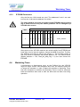
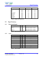
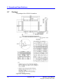
Overview
Figure 2-1 illustrates a simplified block diagram of the VPCLS2. Each function block is briefly explained. For more detailed information about the
submodules, please refer to subsequent sections.
8
IO
Port A
8
8
IO
Port B
IO / Diagnosis
Port C
8
IO / Diagnosis
Port D
Watchdog
Idle Timer
Clock Unit
Shift Register
or E²PROM
48 MHz
Physical Unit
Diagnosis
Port E
Internal
Memory
Microsequencer
Control
Logic
8
Baudrate
Generator
Timer
Figure 2-1 : Blockdiagram of VPCLS2
The VPCLS2 has input/output ports, which can be adapted directly for data
exchange with the periphery. No external microprocessor or additional
software is necessary. The main function blocks of the VPCLS2 include:
The Physical Unit converts the parallel internal data of the VPCLS2 to a
serial data stream for the PROFIBUS and vice versa.
The Baud Rate Generator generates the transmission clock of 9.6 kbit/s
up to 12 Mbit/s for the PROFIBUS interface. The data transmission rate is
recognized and controlled automatically.
The IDLE Timer generates and observes the bus idle time, which is required for synchronizing the bus devices.
The integrated Watchdog Timer permanently observes the VPCLS2 for
addressability. In case of an error, all data ports are set to a logical '0’ in order to avoid malfunctions.
VPCLS2 User Manual
Copyright © profichip GmbH, 2007
Revision 1.03
7
2 Functional Description
The I/O Interface consists of five 8-bit ports. Port A and B are I/O-Ports
only, Port C and D can be configured either as I/O- or diagnosis ports and
Port E is a pure diagnosis port. That is, the VPCLS2 is able to handle up to
32 bit I/O data. The data ports A to D can be configured as inputs or outputs independent from each other. The interface configuration is set via five
pins on the VPCLS2.
The Microsequencer carries out the entire PROFIBUS DP protocol handling. Due the total protocol integration in hardware, baudrates up to 12
Mbit/s can be supported without any restrictions.
The PROFIBUS-specific parameters (Station_Address and Ident_Number)
may be read from an external shift register or serial E²PROM during powerup and after reset. An integrated Control Logic generates the signals for
controlling the external serial shift.
8
Revision 1.03
VPCLS2 User Manual
Copyright © profichip GmbH, 2007
Pin Description
3
3.1
3
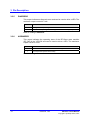
Pin Description
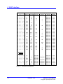
Pin Assignment
Pin
Signal Name
1
XCTS
I(CS)
Clear To Send
PROFIBUS interface: The VPCLS2 is Clear To Send, if the
XCTS signal is active (low)
2
RXD
I(CS)
Receive Data
PROFIBUS interface: input/receive data for VPCLS2
3
RTS
O
Request To Send
The VPCLS2 requests Clear to Send with RTS = ‘1’
4
TXD
O
Transmit Data
PROFIBUS interface: output/transmit data from VPCLS2
5
GND
6
PA0
7
PA1
8
PA2
9
PA3
I(CS) / O
Port A
Port A can be configured as data input or data output port,
depending on the setting of the type pins TYP0..4
(see I/O Interface Configuration Table)
10
PA4
I(CS) / O
Port A
I(CS) / O
Port B
Port B can be configured as data input or data output port,
depending on the setting of the type pins TYP0..4
(see I/O Interface Configuration Table)
I(CS)
Port E
The VPCLS2 receives diagnosis information for the
configurable data ports or user-specific diagnostic
data via this port
I(CS)
Port E
11
PA5
12
GND
13
PA6
14
PA7
15
VCC
16
PB0
17
PB1
18
PB2
19
PB3
20
PB4
21
PB5
22
PB6
23
PB7
24
GND
25
VCC
26
PE0
27
PE1
28
PE2
29
PE3
30
PE4
31
PE5
32
GND
33
VCC
34
PE6
35
PE7
36
GND
In/Out
VPCLS2 User Manual
Copyright © profichip GmbH, 2007
Description
Revision 1.03
9
3 Pin Description
Pin
Signal Name
37
PC0
38
PC1
39
PC2
40
PC3
41
PC4
42
PC5
43
PC6
44
PC7
45
VCC
46
PD0
47
PD1
48
PD2
49
PD3
50
PD4
In/Out
Description
I(CS) / O
Port C
Port C can be configured as data input, data output or
diagnosis port, depending on the setting of the type pins
TYP0..4 (see I/O Interface Configuration Table)
I(CS) / O
Port D
Port D can be configured as data input, data output or
diagnosis port, depending on the setting of the type pins
TYP0..4 (see I/O Interface Configuration Table)
I(CS) / O
Port D
51
PD5
52
GND
53
PD6
54
PD7
55
VCC
56
XRESET
I(CS)
57
RWCONS
O
58
XTEMO
59
XTRI
60
XSREE
61
NC
62
DIAERROR
asynchronous
RESET
Resets the VPCLS2 to a defined initial state (low active)
Read Write
CONSistency
Output ’Read or Write Consistent’, signal for ”preindicating”
a subsequent write or read operation on the data ports.
I(C)
TEst MOde
Test pin: must be set to ‘1’ during normal operation
I(C)
TRI-state
Test pin: must be set to ‘1’ during normal operation
I(C)
Shift Register /
EEprom select
Defines whether an external
shift register or serial E²PROM
is connected to the VPCLS2
’1’ = ext. E²PROM
’0’ = ext. shift register
Not Connected
O
DIAGnosis
ERROR
This output is set when external diagnosis occurs
‘1’ = normal operation
(DATA-EXCH state)
63
NORMOPER
64
GND
65
TYP0
I(C)
66
TYP1
I(C)
67
TYP2
I(C)
68
TYP3
I(C)
69
TYP4
I(C)
70
GND
71
NC
72
CLK
73
VCC
10
O
NORMal OPERation
Operating state indicator
TYPe 0..4
Ports A..D of the VPCLS2 are configured with these pins
(see I/O Interface Configuration Table for details).
‘0’ = after reset and after
each timeout of the WD
timer
Not Connected
I(TS)
CLocK
System Clock Input 48 MHz
Revision 1.03
VPCLS2 User Manual
Copyright © profichip GmbH, 2007
Pin Assignment
Pin
Signal Name
In/Out
74
GND
75
ACA
76
INTERCLK
O
77
INTERCS
O
78
INTERDI
I(TS)
79
INTERDOD
80
VCC
Description
I(C)
O
Address Change
Allowed
When ACA signal is ‘1’, it is possible, to overwrite the
E²PROM contents by a Set_Slave_Add telegram even if the
Real_No_Add_Chg bit is ‘1’.
INTERface
CLocK
VPCLS2 generates clock sequences for the external shift
register / E²PROM via this signal.
INTERface
Chip Select
VPCLS2 selects the external shift register / E²PROM via this
signal.
INTERface
Data Input
VPCLS2 receives input data from the external shift register /
E²PROM via this signal.
INTERface
Data OutloaD
This output serves as a parallel load signal for the external
shift register or a control signal for E²PROM.
Table 3-1 : Pin Assignment
Note:
All signals beginning with X.. are LOW active.
VCC = +5 V
GND = 0 V
Input Levels:
I(C):
I ( CS ) :
I ( TS ) :
CMOS
CMOS, Schmitt-Trigger
TTL, Schmitt-Trigger
Status of pins TYP0..4, ACA and XSREE may only be changed when the
ASIC is without voltage. Dynamical change of those pins while working
is not permitted.
VPCLS2 User Manual
Copyright © profichip GmbH, 2007
Revision 1.03
11
3 Pin Description
3.2
Pinout
PC4
PC5
PC6
PC7
VCC
PD0
PD1
PD2
PD3
PD4
PD5
GND
PD6
PD7
VCC
XRESET
RWCONS
XTEMO
XTRI
XSREE
NC
DIAERROR
NORMOPER
GND
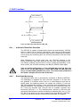
VPCLS2 has a 80-pin PQFP housing with the following pinout:
41
64
TYP0 65
TYP1
TYP2
TYP3
TYP4
GND
NC
CLK
VCC
GND
ACA
INTERCLK
INTERCS
INTERDI
INTERDOD
VCC 80
40 PC3
PC2
PC1
PC0
GND
PE7
PE6
VCC
GND
PE5
PE4
PE3
PE2
PE1
PE0
25 VCC
GND
PB7
PB6
PB5
PB4
PB3
PB2
PB1
PB0
VCC
PA7
PA6
GND
PA5
PA4
PA3
PA2
PA1
PA0
GND
TXD
RTS
24
RXD
XCTS
1
Figure 3-1 : VPCLS2 Pinout
For details about package outline and dimensions see section 8.7 Package.
3.3
3.3.1
Pin Function
CLK
The VPCLS2 needs an external 48 MHz crystal oscillator for proper operation and supports the maximum baud rate of 12 Mbit/s.
3.3.2
RWCONS
This output signal indicates a subsequent consistent write or read access
operation on the data ports. For details about the signal timing, please refer
to section 8.6.4 Consistency Signal RWCONS.
12
Revision 1.03
VPCLS2 User Manual
Copyright © profichip GmbH, 2007
Pin Function
3.3.3
ACA
With ACA signal active (high), it is possible to overwrite the external
E²PROM contents by a Set_Slave_Add telegram even if the bit Real_No_Add_Chg is set (see chapter 5 PROFIBUS DP Interface).
Value
Function
0
current Station_Address cannot be changed in the E²PROM if
Real_No_Add_Chg is set
1
current Station_Address can be changed in the E²PROM even if
Real_No_Add_Chg is set
Table 3-2: Coding of ACA
If the VPCLS2 is operated with an external shift register, this input has no
function.
This input must not be left unconnected.
After power-on it's always possible to overwrite the address once.
3.3.4
XSREE
This input indicates whether the VPCLS2 is operated with an external shift
register or external serial E²PROM.
Value
Function
0
external shift register is used
1
external serial E²PROM is used
Table 3-3: Coding of XSREE
If XSREE = 0, Station_Address and Ident_Number are read from the external shift register after each reset. If XSREE is ‘0’, the Station_Address cannot be changed by a Set_Slave_Add telegram.
If XSREE = 1, Station_Address and Ident_Number are read from the external E²PROM. Station_Address can be changed by a Set_Slave_Add telegram. In this case the E²PROM contents will be updated with the
New_Slave_Add.
If bit No_Add_Chg was set in the Set_Slave_Add service the E²PROM
contents can only be changed again if ACA is ‘1’ or after power-on.
This input must not be left unconnected.
VPCLS2 User Manual
Copyright © profichip GmbH, 2007
Revision 1.03
13
3 Pin Description
3.3.5
DIAERROR
This output indicates a diagnosis error and can be used to drive a LED. The
maximum output current is 4 mA.
Value
Function
0
no diagnosis error pending
1
diagnosis error pending, i.e. a ‘0’ is applied to one of the diagnosis pins
Table 3-4: Coding of DIAERROR
3.3.6
NORMOPER
This output indicates the operating state of the DP-Slave state machine
(DP_SM) in the VPCLS2 and can be used to drive a LED. The maximum
output current is 4 mA.
Value
Function
0
after reset and after each timeout of the watchdog timer
1
normal operation (DATA-EXCH state)
Table 3-5: Coding of NORMOPER
14
Revision 1.03
VPCLS2 User Manual
Copyright © profichip GmbH, 2007
ASIC Interface
4
4.1
4.1.1
4
ASIC Interface
I/O Interface
Port Configuration
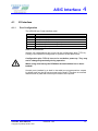
The VPCLS2 has 5 user interface ports:
Port
Function
A
8-bit input or output port
B
8-bit input or output port
C
8-bit input, output or channel diagnosis port
D
8-bit input, output or channel diagnosis port
E
8-bit group diagnosis port
Table 4-1: Port Functions
Various I/O configurations can be set via the configuration pins (TYP0..4).
Coding of the individual configuration is specified in the table below.
Configuration pins TYP0..4 have to be set before power-up. They may
not be changed dynamically during operation.
When using consistency the DP-Master documentation has to be attended!
Unused ports (marked by a dash in the table) are programmed as outputs
by default and may be left unconnected on the board. Therefore no external
resistors and no pads with internal pull resistors are required.
VPCLS2 User Manual
Copyright © profichip GmbH, 2007
Revision 1.03
15
4 ASIC Interface
TYP Pin
Port Configuration / Consistency Requirement
4
3
2
1
0
Port A
Port B
Port C
Port D
Port E
Consist.
0
0
0
0
0
IN
-
-
-
Diagnosis
none
0
0
0
0
1
IN
IN
-
-
Diagnosis
none
0
0
0
1
0
IN
IN
IN
-
Diagnosis
none
0
0
0
1
1
IN
IN
IN
IN
Diagnosis
none
0
0
1
0
0
OUT
-
-
-
Diagnosis
none
0
0
1
0
1
OUT
IN
-
-
Diagnosis
none
0
0
1
1
0
OUT
IN
IN
-
Diagnosis
none
0
0
1
1
1
OUT
IN
IN
IN
Diagnosis
none
0
1
0
0
0
OUT
OUT
-
-
Diagnosis
none
0
1
0
0
1
OUT
OUT
IN
-
Diagnosis
none
0
1
0
1
0
OUT
OUT
IN
IN
Diagnosis
none
0
1
0
1
1
-
-
-
-
Diagnosis
none
0
1
1
0
0
OUT
OUT
OUT
-
Diagnosis
none
0
1
1
0
1
OUT
OUT
OUT
IN
Diagnosis
none
0
1
1
1
0
-
-
-
-
Diagnosis
none
0
1
1
1
1
OUT
OUT
OUT
OUT
Diagnosis
none
1
0
1
0
1
IN
IN
-
-
Diagnosis
overall
1
0
1
1
0
IN
IN
IN
IN
Diagnosis
overall
1
0
1
1
1
OUT
OUT
-
-
Diagnosis
overall
1
1
0
0
0
OUT
OUT
OUT
OUT
Diagnosis
overall
1
1
0
0
1
OUT
OUT
IN
IN
Diagnosis
overall
1
1
1
0
0
IN
IN
IN
-
Diagnosis
overall
1
1
1
0
1
OUT
OUT
OUT
-
Diagnosis
overall
1
1
1
1
0
OUT
OUT
OUT
IN
Diagnosis
overall
1
1
1
1
1
OUT
IN
IN
IN
Diagnosis
overall
Extended
Diagnosis:
1
0
0
0
0
IN
-
Diagnosis
-
Diagnosis
none
1
0
0
0
1
IN
IN
Diagnosis
Diagnosis
Diagnosis
none
1
0
0
1
0
OUT
-
Diagnosis
-
Diagnosis
none
1
0
0
1
1
OUT
OUT
Diagnosis
Diagnosis
Diagnosis
none
1
0
1
0
0
OUT
IN
Diagnosis
Diagnosis
Diagnosis
none
1
1
0
1
0
IN
IN
Diagnosis
Diagnosis
Diagnosis
overall
1
1
0
1
1
OUT
OUT
Diagnosis
Diagnosis
Diagnosis
overall
Table 4-2 : I/O Interface Configuration
16
Revision 1.03
VPCLS2 User Manual
Copyright © profichip GmbH, 2007
I/O Interface
4.1.2
Diagnosis ports
The VPCLS2 offers a maximum of three diagnosis ports depending on the
port configuration. Port E is always a diagnosis port while Ports C and D
are only diagnosis ports if extended diagnosis is selected via the configuration. Port C and D are then used for channel diagnosis.
Generally, all diagnosis ports are low active. A ‘0’ at a diagnosis pin is recognized as a pending diagnosis error.
The user can use all diagnosis ports for user-specific diagnosis. A ‘0’ at a
diagnosis input corresponds to a diagnosis error and sets the VPCLS2 output pin DIAERROR to ‘1’. Output DIAERROR remains set until an error
level is no longer applied to the diagnosis ports. The pin can be used to
drive an LED. The driver power of the output is 4 mA.
The group diagnosis port (Port E) is available as a user-specific diagnosis
port with 8 bits in any configuration. Two operating modes are basically
possible for this port, which can be set by the user with the flag
En_Sammel_Dia in the Set_Prm telegram.
En_Sammel_Dia:
‘0’
A ‘0’ at a pin of Port E leads to a diagnosis error
(DIAERROR output is set to ‘1’)
‘1’
A ‘0’ at pins 0 to 3 of Port E leads only to a diagnosis error if a channel
diagnosis error is also pending at any pin of Port C or Port D.
A ‘0’ at pins 4 to 7 of Port E always leads to a diagnosis error (regardless
of Ports C and D).
Table 4-3: Coding of En_Sammel_Dia
If a port configuration without channel diagnosis (Port C and D) is selected, En_Sammel_Dia must be set to ‘0’.
If configured via the pins TYP0..4, the VPCLS2 also has two channel diagnosis ports (Ports C and D) which can be used to observe each of the remaining I/O ports (Ports A and B). If ports C and D are configured as diagnosis ports, a ‘0’ at one of the pins always leads to a diagnosis error and
DIAERROR is set to ‘1’.
The channel diagnosis ports can also be masked channel-by-channel (each
bit) via mask registers in the Set_Prm telegram. After a reset, all masks are
inactive. An error (‘0’) at a channel diagnosis pin is forwarded only if the
corresponding mask bit is equal to zero.
In order to prevent unconnected inputs of external diagnosis hardware from
leading to a permanent diagnosis error, the VPCLS2 has an internal compare logic. It compares the current diagnosis data with the data last read in
and generates an error only if a diagnosis change has occurred, that is,
VPCLS2 User Manual
Copyright © profichip GmbH, 2007
Revision 1.03
17
4 ASIC Interface
each change is sent to the DP-Master only once (highprior Data_Exchange
response telegram).
‘1’ (+5V) must be applied via pull-up resistors to all unused inputs of
the group diagnosis port (Port E) and all unused inputs of the I/O ports
configured as a channel diagnosis port.
4.2
Shift Register Interface
The VPCLS2 can be connected to an external shift register (XSREE = 0)
containing the Station_Address and Ident_Number. In this case, the integrated control logic generates control sequences for shift registers like the
74HC165 or compatible devices automatically.
4.2.1
Shift Register Control Logic
The shift register control logic is a submodule which is triggered once after
each reset in order to shift in the Ident_Number and Station_Address from
the external shift register.
Signal Name
O
Function
Status after reset
INTERCLK
O
Clock Signal for Shift Register
‘0’
INTERCS
O
Chip-Select for Shift Register
‘1’
INTERDI
I
Data In
INTERDOD
O
Data Out (Shift Register Parallel Load)
‘1’
Table 4-4 : Signals of the Shift Register Interface
The control logic generates a clock signal (INTERCLK), a clock enable signal (INTERCS) and a parallel load signal (INTERDOD) for the external shift
register with the required timing.
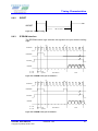
When reading, the data is first loaded parallel into the external shift register
with the INTERDOD signal. From there, the data is clocked serially into the
VPCLS2 internal shift register (see section 'Timing' for detail about the timing).
The shift register controller operates with a clock frequency of 250 kHz. A
read access operation lasts 96 µs.
4.2.2
Shift Register Parameters
The internal shift register of the VPCLS2 is written serially beginning with
bit position 23. Data bits are shifted one position to the right by each clock
pulse.
The required serial data sequence at input INTERDI is shown in Figure 4-1.
First bit to be read is bit 0 of the Station_Address.
18
Revision 1.03
VPCLS2 User Manual
Copyright © profichip GmbH, 2007
E²PROM Interface
Please note that the Station_Address is read BCD-coded, thus permitting values between 1 and 99.
shift direction of internal shift register
23
external
Shift Register
INTERDI
Ident_Number
High Byte
Low Byte
0
Station_Address
BCD-coded
7 6 5 4 3 2 1 0 7 6 5 4 3 2 1 0 7 6 5 4 3 2 1 0
internal
BCD to Binary
Conversion
16
16 Bit Ident_Number
7
Station_Address, binary coded
Figure 4-1 : Shift Register Data Sequence
A total of 24 bits must be stored in the external shift register: 16 bits for
the Ident_Number and 8 bits for the Station_Address.
The Station_Address must be set BCD-coded (values 1 to 99 are permitted). If the VPCLS2 reads the value 0, the Station_Address is assigned the default address 126.
The BCD-coded external address is converted to binary format inside
the VPCLS2 in order to permit the Station_Address to be compared
with the binary-coded destination address (DA) of the PROFIBUS telegrams.
4.3
E²PROM Interface
The VPCLS2 can be connected to an external serial E²PROM (XSREE=1)
with 5V supply, containing the Station_Address and Ident_Number. In this
case, the integrated control logic generates control sequences for E²PROM
like the 93C46 or compatible devices automatically. The device must have
a 16-bit organization and a MICROWIRE compatible interface.
4.3.1
E²PROM Control Logic
The E²PROM control logic is a submodule which is triggered after each reset in order to shift in the Ident_Number and Station_Address from the external E²PROM. If a valid Set_Slave_Add telegram is received the VPCLS2
will program the New_Slave_Add and the new No_Add_Chg bit into the
E²PROM automatically. The program cycle will be verified by comparing the
actual contents of the E²PROM with the expected values. If programming
the E²PROM fails the VPCLS2 reloads the default Station_Address 126
and proceeds operation with that address. The Ident_Number cannot be
changed by a Set_Slave_Add telegram.
VPCLS2 User Manual
Copyright © profichip GmbH, 2007
Revision 1.03
19
4 ASIC Interface
As long as the VPCLS2 is programmed no other Set_Slave_Add service
will be processed by the VPCLS2. These telegrams are responded with “no
resource” (RR). While the E²PROM write cycle is in progress, bit
Diag.E²PROM_Prg_Active is set to ‘1’ in the diagnosis response. If the
control logic can’t program the E²PROM without an Error, bit
Diag.E²PROM_ Fault is set to ‘1’ in the diagnosis response.
If the No_Add_Chg bit was set in the Set_Slave_Add telegram then
changing the Station_Address afterwards is only possible if ACA is ‘1’.
After power-on it's always possible to overwrite the Station_Address at
least once.
Signal Name
O
Function
Status after reset
INTERCLK
O
Clock Signal for E²PROM
‘0’
INTERCS
O
Chip-Select for E²PROM
‘0’
INTERDI
I
Data In
INTERDOD
O
Data Out
‘1’
Table 4-5: Signals of the E²PROM Interface
The control logic generates a clock signal (INTERCLK), a clock enable signal (INTERCS) and a data write signal (INTERDOD) for the external device
with the required timing. Via the data read signal (INTERDI) the VPCLS2
reads in sequentially the data from E²PROM.
Opcode
Address
8
7..6
5..0
READ
1
10
000000
read data of address 0
READ
1
10
000001
read data of address 1
EWEN
1
00
110000
erase / write enable
WRITE
1
01
000000
Command
Startbit
Since the memory has a serial interface, the data, addresses and also the
commands must be transferred serially. Each sequence consist of a Startbit, a 2-bit Opcode and a 6-bit address. Data is read or written only after
such sequence. Each write cycle is preceded by an erase/write enable cycle.
Data
D15..D0
Function
Write data to address 0
Table 4-6: Sequences used for communication with serial E²PROM
The E²PROM controller operates with a clock frequency of 250 kHz. A read
access operation lasts 200 µs and a write access up to 10 ms.
A reset during a write cycle results in undefined E²PROM data.
20
Revision 1.03
VPCLS2 User Manual
Copyright © profichip GmbH, 2007
Watchdog Timer
4.3.2
E²PROM Parameters
Only the first two 16-bit words are used. The addresses 0 and 1 are read
but only the 16-bit word at address 0 is written.
The Ident_Number has to be be written to the E²PROM before connecting to VPCLS2 since only the Station_Address can be changed by a
VPCLS2 write access.
0
Bit Position
15
14
13
12
11
10
9
8
7
0
0
0
0
0
0
0
0
Real_No_Add_Chg
Byte
1
6
5
4
3
2
1
0
Station_Address
Ident_Number
Table 4-7: Coding of E²PROM
After power-on the VPCLS2 reads the two words serially form E²PROM and
loads them into its internal registers. Always the MSB is read first. The Station_Address must have a value in the range of 1..126. All other values (0
and 127) results to operation with default address 126. The default values
(Station_Address = 126, Real_No_Add_Chg = 0) are also stored into
E²PROM.
4.4
Watchdog Timer
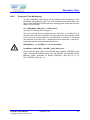
If malfunctions or disturbances occur on the Profibus line, the VPCLS2
might no longer receive valid telegrams and, thus, the module's ports can
no longer be operated. In order to detect this situation a Watchdog Timer
has been integrated. In addition the Watchdog Timer is used for automatic
baud rate detection after reset or after the baud rate has been lost during
operation.
VPCLS2 User Manual
Copyright © profichip GmbH, 2007
Revision 1.03
21
4 ASIC Interface
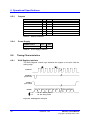
BAUD_SEARCH
WD_Timeout
baudrate detected
BAUD_CONTROL
WD_On = 0
or
WD_DP_CONTROL_Timeout
WD_On = 1
DP_CONTROL
Figure 4-2: Watchdog State Machine (WD_SM)
4.4.1
Automatic Baud Rate Detection
The VPCLS2 is capable of detecting the baud rate automatically. VPCLS2
starts to search for the current transmission rate using the highest baud
rate. If no SD1, SD2 or SD3 telegram was received completely and without
errors during the monitoring time, the VPCLS2 branches to the next lower
baud rate.
After identifying the correct baud rate, the VPCLS2 switches to the
BAUD_CONTROL state and observes the baud rate. Each telegram to its
own Station_Address received with no errors resets the Watchdog. If the
timer expires, the VPCLS2 switches to the BAUD_SEARCH state again.
After an invalid configuration or if the UNLOCK bit in the Set_Prm telegram is set, the DP_SM returns to state WAIT-PRM, but WD_SM does
not go to state BAUD_SEARCH any more. This could cause problems if
the master changes the baud rate at that time.
4.4.2
Baud Rate Monitoring
The detected baud rate is permanently monitored in BAUD_CONTROL.
The Watchdog is triggered by each error-free telegram to its own Station_Address. If a timeout occurs, that is, no valid telegram could be detected within the watchdog period, all outputs are cleared (‘0’) and the
WD_SM automatically branches to the automatic baud rate detection state
(BAUD_SEARCH). The watchdog is used for the DP_CONTROL state, after a Set_Prm telegram was received with an enabled response time
monitoring (WD_On = 1). The watchdog timer remains in the baud rate
monitoring state when the master monitoring is disabled (WD_On = 0). The
DP_SM is not reset when the timer expires in the state BAUD_CONTROL.
That is, the DP-Slave remains in the DATA-EXCH state, for example.
22
Revision 1.03
VPCLS2 User Manual
Copyright © profichip GmbH, 2007
Watchdog Timer
4.4.3
Response Time Monitoring
The DP_CONTROL state serves as the response time monitoring of the
DP-Master (Diag_Master_Add). The used monitoring time results from multiplying both watchdog factors and then multiplying this result with the time
base (1 ms or 10 ms):
TWD = WD_Base × WD_Fact_1 × WD_Fact_2
(see byte 7 of the Set_Prm telegram.)
The user can load the two watchdog factors (WD_Fact_1 and WD_Fact_2)
and the time base that represents a measurement for the monitoring time
via the Set_Prm telegram with any value between 1 and 255. A monitoring
time between 2 ms and 650 s - independent of the baud rate - can be implemented with the permitted watchdog factors.
Setting WD_1 = 1 and WD_2 = 1 is not permitted.
In addition, neither WD_1 nor WD_2 may be set to 0.
If the monitoring time expires, the VPCLS2 goes to BAUD_CONTROL state
again. If another DP-Master takes over the VPCLS2, the Watchdog State
Machine either branches to BAUD_CONTROL (WD_On = 0) or to
DP_CONTROL (WD_On = 1).
VPCLS2 User Manual
Copyright © profichip GmbH, 2007
Revision 1.03
23
4 ASIC Interface
Notes:
24
Revision 1.03
VPCLS2 User Manual
Copyright © profichip GmbH, 2007
PROFIBUS DP Interface
5
5
PROFIBUS DP Interface
The VPCLS2 is a DP-Slave. Response telegrams are generated independently by the VPCLS2 if a valid request telegram is detected to its own Station_Address.
The VPCLS2 only processes valid SD1 or SD2 telegrams addressed to its
own Station_Address. Other telegrams are disregarded. During baud rate
detection mode VPCLS2 uses all telegrams (including SD3 and SD4 telegrams) to find the correct baud rate.
This section only describes those aspects of certain DP telegrams that are
relevant for using with the VPCLS2. For a detailed description of all telegrams, please refer to the PROFIBUS standard IEC 61158-6.
An example GSD-file is given in the appendix.
5.1
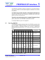
Set_Prm (SAP 61)
The DP-Master transfers parameter data to the VPCLS2 by means of the
Set_Prm telegram (Table 5-1). Bytes 0 to 6 are the standard parameter
bytes according to PROFIBUS standard IEC 61158-6. In addition the
VPCLS2 specific parameter bytes 7 to 11 have to be transferred by the DPMaster.
5
4
3
2
1
0
Freeze_
Req
WD_On
Reserved
Reserved
Reserved
6
Sync_
Req
7
Unlock_
Req
0
Bit Position
Lock_
Req
Byte
Designation
Station Status
3
minTSDR
4
Ident_Number_High
5
Ident_Number_Low
6
Group_Ident
7
0
0
0
0
Dis_Start_
Control
WD_Fact_2
Dis_Stop_
Control
2
WD_Base
WD_Fact_1
En_Sammel_
Dia
1
User_Def_PRM1
8
Mask_Diaport_C
9
Mask_Diaport_D
10
0
0
0
0
0
0
0
0
Reserved1
11
0
0
0
0
0
0
0
0
Reserved2
Table 5-1 : Format of the Set_Prm Telegram
VPCLS2 User Manual
Copyright © profichip GmbH, 2007
Revision 1.03
25
5 PROFIBUS DP Interface
Bits in the Set_Prm telegram marked with ‘0’ are not checked by the
VPCLS2.
5.1.1
User_Def_PRM1
User_Def_PRM1:
bit 7-4
Reserved: To be parameterized with ‘0’
Diagnosis (En_Sammel_Dia): Activates the group diagnosis mode
0 = A ‘0’ at a pin of Port E leads to a diagnosis error
(DIAERROR output is set to ‘1’)
bit 3
1 = A ‘0’ at pins 0 to 3 of Port E leads only to a diagnosis error if a channel
diagnosis error is also pending at any pin of Port C or Port D.
A ‘0’ at pins 4 to 7 of Port E always leads to a diagnosis error (regardless
of Ports C and D).
WD_Base: Watchdog Time Base
bit 2
0 = Watchdog time base is 10 ms (default state)
1 = Watchdog time base is 1 ms
Dis_Stop_Control: Disable Stop-Bit Control
bit 1
0 = Stop-Bit monitoring in the receiver is enabled (default state)
1 = Stop-Bit monitoring in the receiver is disabled
Dis_Start_Control: Disable Start-Bit Control
bit 0
0 = Start-Bit monitoring in the receiver is enabled (default state)
1 = Start-Bit monitoring in the receiver is disabled
Table 5-2 : User_Def_Prm1
If a port configuration without channel diagnosis (port C and D) is selected, En_Sammel_Dia must be set to ‘0’.
5.1.2
Mask_Diaport_C/D
Bytes 8 and 9 of the Set_Prm telegram contain the mask bits for the channel diagnosis ports C and D.
Mask_Diaport_C contains the mask bits for diagnosis Port C and
Mask_Diaport_D contains the mask bits for diagnosis Port D. The mask bits
are assigned to the corresponding bit positions of the channel diagnosis
ports. A ‘1’ at the corresponding bit position disables diagnosis, that is, an
error at that pin will not be forwarded to the master. After Reset all masks
are cleared (‘0’).
If a port configuration without channel diagnosis is selected, both mask
bytes must be set to 00H.
26
Revision 1.03
VPCLS2 User Manual
Copyright © profichip GmbH, 2007
Slave_Diag (SAP 60)
5.1.3
Reserved1/2
These bytes are currently not used and must be programmed as 00H.
5.2
Slave_Diag (SAP 60)
The VPCLS2 sends diagnosis data to the DP-Master by means of this telegram (Table 5-3). In addition to the standard diagnosis bytes 0 to 5, the
VPCLS2 supports 7 bytes of external diagnosis. Diagnosis data is transferred only after a change of the pending data (except for the
Freeze_Mode). A ‘1’ at a bit position indicates that the corresponding event
has occurred.
If Freeze_Mode is activated, the diagnosis data is also frozen. A telegram is thus sent to the DP-Master, but it will contain no change of the
diagnosis data. Diagnosis data will not be updated before another
'Freeze' occurred.
Byte
Bit Position
7
6
5
4
3
2
1
0
Designation
0
Station_Status_1
1
Station_Status_2
2
Station_Status_3
3
Diag_Master_Add
4
Ident_Number_High
5
Ident_Number_Low
PE0
0
0
0
0
0
0
Diag_Reserved_2
12
0
0
0
0
0
0
Diag_E²PROM
PC1
0
PC2
0
PC3
11
PC4
Port D (only with
extended diagnosis,
otherwise 00H)
PC5
10
PC6
Port C (only with
extended diagnosis,
otherwise 00H)
9
PC7
PC0
Diag_Reserved_1
PD0
0
PD1
0
PD2
0
PD3
0
PD4
0
PD5
0
PD6
0
Group diagnosis (Port
E)
Diag.E²PROM
_Prg_Active
0
Diag_Header
PD7
8
1
Diag.E²PROM
_Fault
7
1
PE1
1
PE2
0
PE3
0
PE4
0
PE5
0
PE6
0
PE7
6
Table 5-3 : Format of the Slave_Diag Telegram
VPCLS2 User Manual
Copyright © profichip GmbH, 2007
Revision 1.03
27
5 PROFIBUS DP Interface
Byte 0 – 5:
Bytes 0 to 5 contain the standard Slave_Diag telegram header (refer to IEC
61158-6 for details).
Byte 6: Diag_Header
This byte indicates the number of external diagnosis bytes. This byte is set
to 07H for the VPCLS2.
Byte 7: Group diagnosis
This byte contains the diagnosis data of the signals pending at Port E. A
diagnosis error (‘0’) at a pin of Port E is inverted and forwarded to the
master as a ‘1’ at the corresponding bit position.
Byte 8, 11: Diag_Reserved_1/2
These bytes are reserved. The VPCLS2 always transmits a value of 00H
for those bytes.
Byte 9, 10: Channel diagnosis Port C, Port D
These bytes contain the diagnosis data of the signals pending at Port C
and Port D. A diagnosis error (‘0’) at one of the pins is inverted and forwarded to the master as a ‘1’ at the corresponding bit position. If no extended diagnosis is set via the port configuration, a value of 00H is sent by
the VPCLS2 for those bytes.
Byte 12: Diag_E²PROM:
If the E²PROM write cycle had not been successfully finished, this is,
Slave_Address have not been written without faults, the bit
Diag.E²PROM_Fault is set to ‘1’.
If the E²PROM write cycle is in progress, bit Diag.E²PROM_Prg_Active is
set to ‘1’.
5.3
Chk_Cfg (SAP 62)
The DP-Master transfers the configuration data to the VPCLS2 by means of
this telegram. The VPCLS2 expects 2 bytes of configuration data. The following order must be kept:
Byte
Bit Position
Designation
7
6
5
4
3
2
1
0
0
0/1
0
1
0
0
0
0/1
0/1
Code Byte Outputs
1
0/1
0
0
1
0
0
0/1
0/1
Code Byte Inputs
Table 5-4 : Chk_Cfg Telegram
28
Revision 1.03
VPCLS2 User Manual
Copyright © profichip GmbH, 2007
Global_Control (SAP 58)
Number of outputs
Without consistency
Overall consistency
1
20H
A0H
2
21H
A1H
3
22H
A2H
4
23H
A3H
0
00H
00H
Number of inputs
Without consistency
Overall consistency
1
10H
90H
2
11H
91H
3
12H
92H
4
13H
93H
0
00H
00H
Table 5-5: Coding of Code Byte Outputs
Table 5-6: Coding of Code Byte Inputs
5.4
Global_Control (SAP 58)
The VPCLS2 supports Sync_Mode and Freeze_Mode, i.e. if a Sync Command or Freeze Command is set in the Global_Control telegram, the corresponding function is executed (refer to PROFIBUS standard IEC 61158-6
for more details).
If Freeze_Mode is activated, the diagnosis data is also frozen. A
Slave_Diag response telegram is thus sent to the DP-Master, but it will
contain no change of the diagnosis data. Diagnosis data will not be
updated before another Freeze Command occurred.
5.5
Set_Slave_Add (SAP 55)
The Set_Slave_Add service is only supported in E²PROM mode. If using an
external shift register, this service will be acknowledged negative. The permitted address range is 0 to 125.
If a valid Set_Slave_Add telegram is received the VPCLS2 will program the
New_Slave_Add and the new No_Add_Chg bit into the E²PROM automatically. The program cycle will be verified by comparing the actual contents of
the E²PROM with the expected values.
If programming of the E²PROM fails the VPCLS2 reloads the default
PROFIBUS address (126) and proceeds operation with that address. An
E²PROM programming fault is indicated in the diagnosis response with bit
Diag.E²PROM_Fault set to ‘1’.
VPCLS2 User Manual
Copyright © profichip GmbH, 2007
Revision 1.03
29
5 PROFIBUS DP Interface
As long as the E²PROM is programmed no other Set_Slave_Add service
will be processed by the VPCLS2. While the E²PROM Memory write cycle
is in progress, bit Diag.E²PROM_Prg_Active is set to ‘1’ in the diagnosis response.
If the No_Add_Chg bit was set in the Set_Slave_Add telegram then
changing the Station_Address afterwards is only possible if ACA is ‘1’.
After power-on it's always possible to overwrite the slave address at
least once.
5.6
Other Services (SAP 56, 57, 59)
In addition the VPCLS2 supports the following PROFIBUS services:
RD_Input (SAP 56)
RD_Output (SAP 57)
Get_Cfg (SAP 59)
30
Revision 1.03
VPCLS2 User Manual
Copyright © profichip GmbH, 2007
GND
VCC
10
11
12
13
14
3
4
5
6
1
15
2
VPCLS2 User Manual
Copyright © profichip GmbH, 2007
QH
QH#
Revision 1.03
C
C
9
7
C
C
BCD Switch
HIGH Byte
PNO
Ident_Number
74HCT165
SER
A
B
C
D
E
F
G
H
SH/LD#
CLKINH
CLK
8
8
4
2
1
8
4
2
GND
QH
QH#
GND
10K
LOW Byte
PNO
Ident_Number
74HCT165
SER
A
B
C
D
E
F
G
H
SH/LD#
CLKINH
CLK
10K
10
11
12
13
14
3
4
5
6
1
15
2
S1_D7
S1_D6
S1_D5
S1_D4
S1_D3
S1_D2
S1_D1
S1_D0
9
7
S1_D7
S1_D6
S1_D5
S1_D4
S1_D3
S1_D2
S1_D1
S1_D0
SRDO
SRCS
SRCLK
10
11
12
13
14
3
4
5
6
1
15
2
QH
QH#
Station_Address
74HCT165
SER
A
B
C
D
E
F
G
H
SH/LD#
CLKINH
CLK
9
7
78
INTERDI
GND
60
XSREE = '0' for Shiftregister
XSREE
VPCLS2
6
4
2
1
8
4
2
1
1
LOW or HIGH
level must be
applied to the
pins depending
on the Identnumber
SRDO
SRCS
SRCLK
79
76 INTERDOD
77 INTERCLK
INTERCS
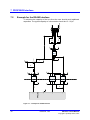
6.1
LOW or HIGH
level must be
applied to the
pins depending
on the Identnumber
SRDO
SRCS
SRCLK
Hardware Interface
6
Hardware Interface
Shift Register Interface
Figure 6-1: Shift Register Example
31
GND
100n
32
GND
Revision 1.03
GND
VCC
4
3
1
8
GND
VCC
RESET
TL7705
GND RESIN#
CT
REF RESET#
SENSE
93C46/47
GND
ORG
NC
VCC
VCC
5
6
7
8
2
6
5
7
DO
DI
SK
CS
VCC
4
3
2
1
GND
4K7
VCC
GND
VCC
3K3
3K3
1K
GND
GND
10K
GND
BASP
10K
GND
BC817
10K
GND
47n
10K
56
78
79
76
77
XRESET
60
VCC
75
VCC
62
63
XSREE = '1' for E²PROM
XSREE
ACA
DIAERROR
NORMOPER
VPCLS2
INTERDI
INTERDOD
INTERCLK
INTERCS
820
820
GND
VCC
6.2
10u
VCC
6 Hardware Interface
E²PROM, LEDs and Reset
Figure 6-2: E²PROM Example
VPCLS2 User Manual
Copyright © profichip GmbH, 2007
UART
6.3
UART
The transmitter converts the parallel data structure into a serial data flow.
Signal Request-to-Send (RTS) is generated before the first character. The
XCTS input is available for connecting a modem. After RTS active, the
transmitter must hold back the first telegram character until the modem activates XCTS. XCTS is checked again after each character.
The receiver converts the serial data flow into the parallel data structure
and scans the serial data flow with the four-fold transmission speed. Stop
bit testing can be switched off for test purposes ('Dis_Stop_Control = 1' in
mode register 0 or Set_Prm telegram for DP). One requirement of the
PROFIBUS protocol is that no rest states are permitted between the telegram characters. The VPCLS2 transmitter ensures that this specification is
maintained.
The synchronization of the receiver starts with the falling edge of the Start
bit. The Start bit is checked again in the middle of the bit-time for low level.
The data bits, the Parity and the Stop bit are also scanned in the middle of
the bit-time. To compensate for the synchronization error, a repeater generates a ±25% distortion of the stop bit at a four-fold scan rate. In this case
the VPCLS2 should be parameterized with 'Dis_Start_Control = 1'
(‘Set_Prm telegram’ for DP) in order to increase the permissible distortion
of the stop bit.
6.4
ASIC Test
The XTEMO pin is used to enable internal test modes of the VPCLS2 during production of the chip. All output and I/O pins of VPCLS2 can be
switched in the high-resistance state via the XTRI test pin.
Pin
Name
58
XTEMO
59
XTRI
Value
Function
GND
test modes enabled
VCC
test modes disabled (normal operation mode)
GND
all outputs are high-resistance
VCC
normal operation mode
Figure 6-3: Test Ports
These inputs must not be left unconnected.
VCC must be applied to the XTEMO and XTRI pin in normal operation
mode.
The test modes are for testing the chip on automatic test equipment
during chip production only (not in the target hardware environment!).
Those test modes are NOT user accessible.
VPCLS2 User Manual
Copyright © profichip GmbH, 2007
Revision 1.03
33
6 Hardware Interface
Notes:
34
Revision 1.03
VPCLS2 User Manual
Copyright © profichip GmbH, 2007
PROFIBUS Interface
7
7.1
7
PROFIBUS Interface
Pin Assignment
The data transmission is performed in RS485 operating mode (i.e., physical
RS485). VPCLS2 provides the PROFIBUS interface signals listed in Table
below.
Signal Name
I/O
Type
Function
XCTS
I
CMOS
Clear to Send
RXD
I
CMOS
Receive Data
RTS
O
CMOS
Request to Send
TXD
O
CMOS
Transmit Data
Table 7-1: PROFIBUS Interface Signals
Before transmitting, the VPCLS2 sets the RTS signal to ‘1’ and then loads
the transmit buffer of the UART with the first character to be transmitted.
The UART holds back the first telegram character until signal XCTS is active (‘0’). On completion of transmission (transmit buffer is empty and the
last stop bit is sent), the RTS signal is de-asserted (‘0’).
The PROFIBUS interface is a 9-way, sub D, plug connector with the following pin assignment.
Pin 1 - Free
Pin 2 - Free
Pin 3 - B line
Pin 4 - Request to send (RTS)
Pin 5 - Ground 5V (M 5 )
Pin 6 - Potential 5V (floating P5 )
Pin 7 - Free
Pin 8 - A line
Pin 9 - Free
The cable shield must be connected to the plug connector housing.
The free pins are described as optional in IEC 61158-2.
CAUTION:
The pin names A and B on the plug connector refer to the signal names in
the RS485 standard and not the pin names of driver ICs.
Keep the wires from driver to connector as short as possible.
VPCLS2 User Manual
Copyright © profichip GmbH, 2007
Revision 1.03
35
36
Revision 1.03
TxD
RxD
XCTS
4
2
1
GND
10K
470R
GND
VCC
GND
4
2
1
5
7
6
8
2
3
GND1
VI
VCC1
GND2
NC
VO
VCC2
A
K
5
7
6
8
4
2
1
5
7
6
8
HCPL0710
GND2
NC
VO
VCC2
HCPL0710
GND1
VI
VCC1
HCPL0601
GND
VE
VO
VCC
GND_I
VCC_I
GND_I
330R
1K2
GND_I
1K2
GND_I
BC807C
1
2
3
4
DS75176
R
RE#
DE
D
VCC
A
B
GND
8
6
7
5
GND_I
VCC_I
330R
100K
100K
VCC_I
GND_I
DGND
CNTR_N
CNTR_P
L2_N
L2_P
P24
M24
P5V
SHIELD
5
9
4
8
3
7
2
6
1
SUBD_BU_PROFIBUS
11
10
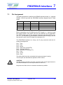
7.2
VPCLS2
RTS
3
VCC_I
VCC_I
7 PROFIBUS Interface
Example for the RS485 Interface
To minimize the capacity of the bus lines the user should avoid additional
capacities. The typical capacity of a bus station should be 15...25 pF.
Figure 7-1 : Example for RS485 Interface
VPCLS2 User Manual
Copyright © profichip GmbH, 2007
8
Operational Specifications
8
8.1
Operational Specifications
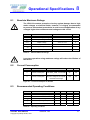
Absolute Maximum Ratings
The VPCLS2 contains protective circuitry against damage due to high
static voltages or electrical fields; however, it is highly recommended
to preserve all standard precautions in order to avoid application of any
voltages higher than maximum-rated voltages to this circuit.
SYMBOL
PARAMETER
RATING
UNITS
VCC
DC Power Supply Voltage
-0.3 to 6.0
V
VIN
Input Voltage
-0.3 to VCC+0.3
V
VOUT
Output Voltage
-0.3 to VCC+0.3
V
IOUT
DC Output Current
See Table 8-4
mA
TSTG
Storage Temperature
-40 to 150
°C
RΘ(JA)
RΘ Junction-Ambient (still air)
43.8
°C/W
Table 8-1 : Absolute Maximum Ratings
Long-term operation using maximum ratings will reduce the lifetime of
the device.
8.2
Current Consumption
SYMBOL
PARAMETER
CONDITION
LIMITS
UNITS
IA
Current Consumption
12MBit/s transmission rate,
state WAIT_PRM, no bus traffic
65
mA
IA
Current Consumption
12MBit/s transmission rate,
all ports configured as outputs
and driven active high
150
mA
UNITS
Figure 8-1 : Current Consumption of VPCLS2
8.3
Recommended Operating Conditions
SYMBOL
PARAMETER
MIN
TYP
MAX
VCC
DC Power Supply Voltage
4.50
5.00
5.50
V
GND
Circuit Ground
0
0
0
V
VIN
Input Voltage
0
VCC
V
TJ
Junction Operating Temperature
-40
125
°C
TA
Ambient Temperature
-40
85
°C
25
Table 8-2 : Operating Conditions
VPCLS2 User Manual
Copyright © profichip GmbH, 2007
Revision 1.03
37
8 Operational Specifications
8.4
DC Electrical Characteristics Specification of I/O cells
SYMBOL
PARAMETER
VCC
DC Power Supply Voltage
VIL
Input Low Voltage
VIH
Input High Voltage
VIL
Input Low Voltage
VIH
Input High Voltage
VT
Switching Threshold
VTVT+
VTVT+
Schmitt Trigger Negative Going
Threshold Voltage
Schmitt Trigger Positive Going
Threshold Voltage
Schmitt Trigger Negative Going
Threshold Voltage
Schmitt Trigger Positive Going
Threshold Voltage
CONDITIONS
MIN
TYP
MAX
UNITS
4.50
5.00
5.50
V
0.3×VCC
V
CMOS
0.7×VCC
V
TTL
0.8
2.0
V
V
CMOS
2.4
V
TTL
1.4
V
1.8
V
1.5
CMOS
3.0
0.9
3.4
1.1
V
V
TTL
1.8
2.1
V
0.4
V
VOL
Output Low Voltage
IOL = 2 ~24 mA
VOH
Output High Voltage
IOH = -2 ~ -24 mA
3.5
IIN
Input Leakage Current
VIN = VCC or 0
-10
±1
10
µA
IOZ
3-State Output Leakage Current
-10
±1
10
µA
CIN
Input Capacitance
3
5
pF
COUT
Output Capacitance
3.5
5
pF
CBID
Bi-directional Buffer Capacitance
3.5
5
pF
V
Table 8-3 : DC Characteristics of I/O cells
38
Revision 1.03
VPCLS2 User Manual
Copyright © profichip GmbH, 2007
Signal Summary
SIGNAL
DRIVER TYPE
DRIVER STRENGTH
MAX. CAP. LOAD
Tristate
4 mA
50 pF
PA[7..0] to PD[7..0]
TXD
Tristate
8 mA
50 pF
RTS
Tristate
8 mA
50 pF
NORMOPER
Tristate
4 mA
50 pF
DIAERROR
Tristate
4 mA
50 pF
INTERCLK
Tristate
4 mA
50 pF
INTERCS
Tristate
4 mA
50 pF
INTERDOD
Tristate
4 mA
50 pF
RWCONS
Tristate
4 mA
50 pF
Table 8-4 : Ratings of the Output Drivers
8.5
8.5.1
Signal Summary
Bidirectional Signals
BIDIRECTIONAL SIGNALS QTY.
I/O
TYPE
PA[7...0]
8
I/O
CMOS Schmitt Trigger, 4 mA Buffer
PB[7...0]
8
I/O
CMOS Schmitt Trigger, 4 mA Buffer
PC[7...0]
8
I/O
CMOS Schmitt Trigger, 4 mA Buffer
PD[7...0]
8
I/O
CMOS Schmitt Trigger, 4 mA Buffer
Table 8-5 : Bidirectional Signals of VPCLS2
8.5.2
Inputs
INPUTS
QTY.
I/O
TYPE
ACA
1
IN
CMOS
PE[7..0]
8
IN
CMOS Schmitt Trigger
INTERDI
1
IN
TTL Schmitt Trigger
RXD
1
IN
CMOS Schmitt Trigger
XTEMO
1
IN
CMOS
XTRI
1
IN
CMOS
XSREE
1
IN
CMOS
TYP[4..0]
5
IN
CMOS
CTS
1
IN
CMOS Schmitt Trigger
XRESET
1
IN
CMOS Schmitt Trigger
CLK
1
IN
TTL Schmitt Trigger
Table 8-6 : Inputs of VPCLS2
VPCLS2 User Manual
Copyright © profichip GmbH, 2007
Revision 1.03
39
8 Operational Specifications
8.5.3
Outputs
OUTPUTS
QTY.
I/O
DIAERROR
1
OUT
TYPE
4 mA Buffer
INTERCS
1
OUT
4 mA Buffer
NORMOPER
1
OUT
4 mA Buffer
RWCONS
1
OUT
4 mA Buffer
RTS
1
OUT
8 mA Buffer
TXD
1
OUT
8 mA Buffer
Table 8-7 : Outputs of VPCLS2
8.5.4
Power Supply
POWER SUPPLY
VCC
GND
7
9
Table 8-8 : Power Supply of VPCLS2
8.6
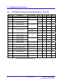
8.6.1
Timing Characteristics
Shift Register Interface
The Shift Register control logic switches the signals to the pins with the
trailing edge.
c
d
INTERCLK
INTERDOD
(parallel load)
INTERCS
(clock enable)
INTERDI
c
d
2 us
4 us
D0
D1
D2
D3
D4
D5
D6
D21
D22
D23
D0 - D7 : Station_Address
D8 - D23: Ident_Number
Figure 8-2: Shift Register read cycle
40
Revision 1.03
VPCLS2 User Manual
Copyright © profichip GmbH, 2007
Timing Characteristics
8.6.2
RESET
XRESET
min. 416 ns
Figure 8-3 : RESET Timing
8.6.3
E²PROM Interface
The E²PROM control logic switches the signals to the pins with the trailing
edge.
c
d
INTERCLK
INTERDOD
INTERCS
D15
INTERDI
8
c
d
2 us
4 us
Startbit
7
6
5
4
2 bit
Opcode
3
2
1
D14
D13
D0
0
6 bit Address
Data
Figure 8-4: E²PROM read cycle for address 0
c
d
INTERCLK
INTERDOD
INTERCS
D15
INTERDI
8
c
d
2 us
4 us
Startbit
7
6
2 bit
Opcode
5
4
3
2
6 bit Address
1
D14
D13
D0
0
Data
Figure 8-5: E²PROM read cycle for address 1
VPCLS2 User Manual
Copyright © profichip GmbH, 2007
Revision 1.03
41
8 Operational Specifications
c
d
INTERCLK
INTERDOD
INTERCS
8
c
d
2 us
Startbit
4 us
6
7
5
3
4
2 bit
Opcode
2
1
0
6 bit Address
Figure 8-6: E²PROM erase / write enable cycle
After erase / write enable cycle the write cycle follows immediately.
d
c
INTERCLK
INTERDOD
D15
D14
D13
D0
INTERCS
INTEDI
8
c
d
2 us
4 us
Startbit
7
6
5
2 bit
Opcode
3
4
2
6 bit Address
1
0
Data
n
INTERCLK
INTERDOD
INTERCS
INTERDI
READY
write cycle time
(max. 10 ms)
min. 3 clock cycle
n
Figure 8-7: E²PROM write cycle
42
Revision 1.03
VPCLS2 User Manual
Copyright © profichip GmbH, 2007
Timing Characteristics
8.6.4
Consistency Signal RWCONS
Write timing: The user can switch external latches transparently with the
RWCONS signal in order to accept new data from the output ports simultaneously.
RWCONS
WRITE IO
(internal)
Port Data
1
2
Figure 8-8 : RWCONS WRITE cycle
Read timing: The user can freeze external latches with the RWCONS signal in order to accept consistent data at the input ports of the VPCLS2
("snapshot" option).
RWCONS
READ IO
(internal)
Port Data
3
4
Figure 8-9 : RWCONS READ cycle
No.
Symbol
Parameter
Unit
1
RWCONS SETUP
RWCONS active to internal write
1
Tbit*
2
RWCONS HOLD
RWCONS inactive to internal write
1
Tbit*
3
D SETUP
Data – Setup after RWCONS active
1
Tbit*
4
D HOLD
Data – Hold after RWCONS inactive
0
Tbit*
*: 1 Tbit =104µs at 9,6kBd , 1 Tbit = 83ns at 12MBd
Table 8-9 : RWCONS Timing
VPCLS2 User Manual
Copyright © profichip GmbH, 2007
Revision 1.03
43
8 Operational Specifications
8.7
Package
The package of the VPCLS2 is lead-free.
Figure 8-10 : Package Drawing
44
Revision 1.03
VPCLS2 User Manual
Copyright © profichip GmbH, 2007
Processing Instructions
8.8
8.8.1
Processing Instructions
ESD Protection
The ESD safety standards have to be preserved for all electronic components at any time.
The VPCLS2 contains protective circuitry against damage due to high
static voltages or electrical fields; however, it is highly recommended
to preserve all standard precautions in order to avoid application of any
voltages higher than maximum-rated voltages to this circuit.
8.8.2
Soldering Pre-Conditioning
All PQFP components are subject to the risk of cracking and must be handled accordingly.
The VPCLS2 must be dried before processing for 24 hours at 125°C and
then processed within a period of 48 hours. This drying process may
be carried out only once due to preserve solderability of the component. Please ensure that the pins of the VPCLS2 are not bent. Proper
processing can be guaranteed only if the deviation from flatness is less
than 0.1 mm.
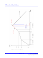
8.8.3
Reflow Soldering Profile
Please see Table 8-10 and Figure 8-11 for details about the lead-free
package reflow soldering conditions.
Profile Feature
Description
1.7~2.3 ℃/sec
Average ramp-up rate
(Root temperature to 130 ℃)
Preheat
-Temperature Minimum
-Temperature Maximum
-Time(min to max)
Time maintained above:
-Temperature
-Time
130℃
183℃
90~120 sec
220 ℃
80~120 sec
Peak Temperature
260 ℃ / -5 ℃
Time within 5
10~30 sec
of actual peak temperature
Ramp-down rate
4 ℃/sec (max )
Time 25 °C to peak temperature
8 min (max)
Table 8-10 : Reflow Soldering Conditions
VPCLS2 User Manual
Copyright © profichip GmbH, 2007
Revision 1.03
45
8 Operational Specifications
Figure 8-11 : Reflow Soldering Profile
46
Revision 1.03
VPCLS2 User Manual
Copyright © profichip GmbH, 2007
GSD-File Example
9
9
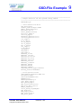
GSD-File Example
;===========================================================
; Sample GSD-file for PB systems using VPCLS2
;===========================================================
#PROFIBUS_DP
; <Unit-Definition-List>
GSD_Revision=1
Vendor_Name="Sample GmbH"
Model_Name="XYZ1000"
Revision="V1.0"
Ident_Number=0x1234
Protocol_Ident=0
Station_Type=0
Hardware_Release="1.0"
Software_Release="1.0"
9.6_supp=1
19.2_supp=1
45.45_supp=1
93.75_supp=1
187.5_supp=1
500_supp=1
1.5M_supp=1
3M_supp=1
6M_supp=1
12M_supp=1
MaxTsdr_9.6=60
MaxTsdr_19.2=60
MaxTsdr_45.45=250
MaxTsdr_93.75=60
MaxTsdr_187.5=60
MaxTsdr_500=100
MaxTsdr_1.5M=150
MaxTsdr_3M=250
MaxTsdr_6M=450
MaxTsdr_12M=800
Implementation_Type="VPCLS2"
Bitmap_Device="XYZxxxx"
; Slave-Specification:
OrderNumber="XYZ1000-0AH5-Y0"
Periphery="XYZ"
OffsetFirstMPDBlock=0
ETERDelay=0
MaxResponseDelay=0
Sync_Mode_supp=1
Auto_Baud_supp=1
Min_Slave_Intervall=0
Max_Diag_Data_Len=13
Modul_Offset=0
Slave_Family=1@TdF@XYZ
Max_Module=2
Max_Input_Len=0
Max_Output_Len=2
Max_Data_Len=2
VPCLS2 User Manual
Copyright © profichip GmbH, 2007
Revision 1.03
47
9 GSD-File Example
; UserPrmData: Length and Preset:
User_Prm_Data_Len=5
User_Prm_Data = 0x00,0x00,0x00,0x00,0x00
Ext_User_Prm_Data_Const(0)=0x00,0x00,0x00,0x00,0x00
; Unit-Diagnostics:
Unit_Diag_Bit(0000)="short circuit
Unit_Diag_Bit(0001)="overload
Unit_Diag_Bit(0002)="short circuit
Unit_Diag_Bit(0003)="overload
Ch
Ch
Ch
Ch
0- 7"
0- 7"
8-15"
8-15"
; <Module-Definition-List>
Module="2 Byte Out, 0 Byte In" 0x21,0x00
EndModule
48
Revision 1.03
VPCLS2 User Manual
Copyright © profichip GmbH, 2007
Revision History
Revision History
Version
Date
Page
Remarks
V1.00
22.06.2005
V1.01
31.01.2007
10
First Release
Wrong signal name for pin 45 corrected.
V1.02
04.10.2007
11
Wrong signal name for pin 80 corrected.
V1.03
17.11.2008
44
Minor changes in package dimensions (L1)
VPCLS2 User Manual
Copyright © profichip GmbH, 2007
Revision 1.03
49
profichip GmbH
Einsteinstrasse 6
91074 Herzogenaurach
Germany
Phone :
Fax:
+49.9132.744-200
+49.9132.744-204
www.profichip.com


![ZXmore-V11-ConstructionKit [1144.78] KB](http://vs1.manualzilla.com/store/data/005859049_1-e30fafda14586d16f36a324828eeb8d9-150x150.png)