1
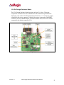
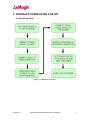
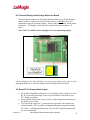
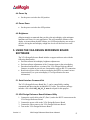
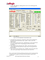
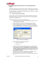
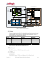
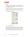
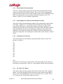
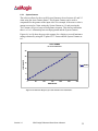
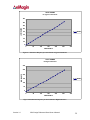
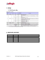
VGA DESIGN REFERENCE BOARD
For Use with all eMagin VGA OLED Microdisplays
P/N: EMA-200009
USER’S MANUAL
VERSION 1.0
Version 1.0
VGA Design Reference Board User’s Manual
i
TABLE OF CONTENTS
1.
INTRODUCTION .................................................................................................................................. 1
2.
FEATURES .......................................................................................................................................... 1
2.1.
Software Features ....................................................................................................................... 1
3.
SYSTEM REQUIREMENTS & SPECIFICATIONS.............................................................................. 1
3.1.
System Requirements ................................................................................................................. 1
3.2.
VGA Design Reference Board..................................................................................................... 2
4.
INTERFACE CONNECTIONS & SETUP............................................................................................. 3
4.1.
Setup Flow Chart ......................................................................................................................... 3
4.2.
Connect Display to the Design Reference Board ........................................................................ 4
4.3.
Setup PC for Proper Video Output .............................................................................................. 4
4.4.
Power Up ..................................................................................................................................... 5
4.5.
Power Down ................................................................................................................................ 5
4.6.
Brightness .................................................................................................................................... 5
5.
USING THE VGA DESIGN REFERENCE BOARD SOFTWARE....................................................... 5
5.1.
Serial Interface Command Set..................................................................................................... 5
5.2.
VGA Design Reference Board Software Utility............................................................................ 5
5.2.1.
5.3.
Hardware Protocol..................................................................................................................................7
Downloading New Firmware Versions to the Design Reference Board ...................................... 8
5.3.1.
6.
Using the Firmware Download Utility......................................................................................................8
ADVANCED USER INFORMATION.................................................................................................... 9
6.1.
Microcontroller ............................................................................................................................. 9
6.2.
I2C bus ......................................................................................................................................... 9
6.3.
System Hardware Overview ........................................................................................................ 9
6.4.
Voltages ..................................................................................................................................... 10
6.5.
Bias Control ............................................................................................................................... 10
6.6.
VCOM Mode .............................................................................................................................. 10
6.7.
Gamma ...................................................................................................................................... 11
6.7.1.
6.7.2.
6.7.3.
6.7.4.
6.7.5.
6.7.6.
Gamma Coefficients GC(0-8) ...............................................................................................................11
Preset Gamma Table descriptions .......................................................................................................12
Using “Update LUT” Button for Auto-Gamma Correction .....................................................................12
Loading the LUT from a file ..................................................................................................................12
The “Read LUT” Button .......................................................................................................................12
System Gamma....................................................................................................................................13
7.
FPGA.................................................................................................................................................. 15
7.1.
FPGA Register Map................................................................................................................... 15
8.
REVISION HISTORY ......................................................................................................................... 15
Version 1.0
VGA Design Reference Board User’s Manual
ii
List of Figures
Figure 3-1 VGA Design Reference Board ..................................................................................... 2
Figure 4-1 DRK Setup Flow Chart................................................................................................ 3
Figure 5-1 Firmware download utility ........................................................................................... 8
Version 1.0
VGA Design Reference Board User’s Manual
iii
1. INTRODUCTION
The VGA Design Reference Board provides the user with a highly compact,
portable way of operating an eMagin VGA OLED Microdisplay. This product
was designed to deliver a complete tool for developers to evaluate and integrate
eMagin VGA microdisplays into new products. The included software package
provides access to the microdisplay’s on-board register settings from any
Windows-based PC through a serial port and supports all three different types of
VGA OLED Microdisplays:
•
VGA Monochrome White OLED-XL with glass cover (P/N: EMA-100600-01)
•
VGA Color OLED-XL with glass cover (P/N: EMA-100601-01)
•
VGA Monochrome Green OLED-XL with glass cover (P/N: EMA-100602-01)
2. FEATURES
•
•
•
•
DVI-HDMI Video Input
RS-232 (serial) interface allows access to microdisplay registers
Supporting Software (Windows)
ON/OFF power switch
2.1. Software Features
•
•
•
•
•
Read/write capabilities allow adjustments of microdisplay register settings to
fine-tune image characteristics
Software register control over the cathode voltage (Vcommon) input
Software register control over the microdisplay’s brightness
Download and install new firmware files into your VGA Design Reference
Board for easy upgrades and expanded functionality
Save feature stores custom register settings for convenience
3. SYSTEM REQUIREMENTS & SPECIFICATIONS
3.1. System Requirements
•
•
Version 1.0
For digital RGB inputs: A PC capable of producing a digital video output
compliant with the DVI standard.
Support software requires a Windows PC with an RS-232 serial port
VGA Design Reference Board User’s Manual
1
3.2. VGA Design Reference Board.
The VGA Design Reference Board is shown in figure 3-1 below. The major
components are labeled for easier identification. The minimum requirements for
displaying video on the VGA Design Reference Board are; a +9 Volt power supply
connected to the power connector, a digital video source connected to the HDMI
connector (A DVI to HDMI adapter is included with the unit) and an VGA OLED
connected to the display connector (J12).
Figure 3-1 VGA Design Reference Board
Version 1.0
VGA Design Reference Board User’s Manual
2
4. INTERFACE CONNECTIONS & SETUP
4.1. Setup Flow Chart
Figure 4-1 DRK Setup Flow Chart
Version 1.0
VGA Design Reference Board User’s Manual
3
4.2. Connect Display to the Design Reference Board
The microdisplay connects to the Design Reference Board via a 50-pin board-toboard connector. The present version of the connector is NOT keyed so it is
important to correctly orient the display. Refer to the picture below for the proper
orientation. . The Display Carrier board is connected as shown in figure 4-2
below.
Note: The VGA OLED can be damaged if it is not connected properly.
Figure 4-2 Display Carrier Board Connection Orientation
Lift the display by its sides and take care not to press on the active area or leave
fingerprint marks on it. Insert the display into the Design Reference Board.
4.3. Setup PC for Proper Video Output
•
•
•
Version 1.0
The default compatible resolution is VGA (640x480) with a refresh rate of 60
Hz. If you are using this input set the video resolution for 640x480 in your
PC’s display properties.
Ensure that the refresh rate to set to 60 Hz, or other supported refresh rate per
the display specification.
If you are using a laptop PC, you may need to export the video signal to an
external monitor. This is usually accomplished through a keypress including
the Fn key + a designated function key. See your PC’s operation instructions
for more information.
VGA Design Reference Board User’s Manual
4
4.4. Power Up
•
Set the power switch to the ON position.
4.5. Power Down
•
Set the power switch to the OFF position.
4.6. Brightness
eMagin strongly recommends that you drive the microdisplay at the minimum
luminance necessary for your application. This will extend the lifetime of the
display to its maximum possible lifetime. As OLED microdisplays are emissive
devices, driving the microdisplay at high bias levels will decrease its overall
lifetime.
5. USING THE VGA DESIGN REFERENCE BOARD
SOFTWARE
The VGA Design Reference Board includes a support software suite with the
following functionality.
• Perform software microdisplay brightness adjustments
• Perform software adjustments of the Vcommon input to the microdisplay
• Download and install new versions of the VGA Design Reference Board
firmware to update or provide new functionality using an RS-232 connection
• Read/write register values to the microdisplay and FPGA to control various
characteristics (see your microdisplay’s User Specification for more
information)
5.1. Serial Interface Command Set
The VGA Design Reference Board Rev. 3 can be controlled by sending
commands and data using the included RS-232 cable. The software package
includes a file called VGA_SW_V1_2.exe developed for this purpose.
5.2. VGA Design Reference Board Software Utility
1. Connect the serial cable to the PC (Port 1) and to the RS232 connector on the
VGA Design Reference Board
2. Connect the power cable to the VGA Design Reference Board
3. Connect the video source to the VGA Design Reference Board
4. Turn on the VGA Design Reference Board
Version 1.0
VGA Design Reference Board User’s Manual
5
5. Start the VGA_SW_V1_2.exe application and a screen should appear like
that shown below:
Figure 5-1 VGA Design Reference Board Software Utility
6. The application communicates with the PIC on the VGA Design Reference
Board and reads the initial status of the “OLED”, “FPGA” and “VPG”
shutdown pins.
7. The read/write buttons shown in the “OLED Registers” panel will read/write
the register settings in their corresponding boxes from/to the OLED
microdisplay.
8. The read/write buttons displayed in the “FPGA” panel will read/write the
settings displayed in the register boxes from/to the VGA Design Reference
Board’s FPGA.
9. The read/write buttons displayed in the “GAMMA” panel will read/write the
values used in generating a Gamma table that resides in the FPGA
Direct control of the VGA Design Reference Board can also be implemented into
a customer specific application using the following hardware protocol and
command set.
Version 1.0
VGA Design Reference Board User’s Manual
6
5.2.1. Hardware Protocol
•
•
•
Version 1.0
1 stop bit, no parity
9600 baud
No hardware handshake
VGA Design Reference Board User’s Manual
7
5.3. Downloading New Firmware Versions to the Design Reference
Board
The ability to download new versions of the firmware ensures that you will have
the latest functionality without having to send your VGA Design Reference Board
for reprogramming. A utility that downloads and installs new firmware versions is
included in the software package.
5.3.1.
Using the Firmware Download Utility
Firmware files can be downloaded as hex files. Before attempting to download
and install new firmware versions make sure that you have received a firmware
hex file from an eMagin source.
To load your firmware files, follow the following steps:
1. Connect the serial cable to the PC and to the RS232 connector on the
VGA Design Reference Board
2. Connect the power cable to the VGA Design Reference Board.
3. Connect your video source to the VGA Design Reference Board.
4. Start the VGA_SW_V1_2.exe application. Select the “Bootloader”
menu at the top of the form. A window should appear like that below:
Figure 5-1 Firmware download utility
5. Make sure the following settings are shown
a. Processor = 18F2523
b. Com Port = 1
6. Click the “Program” button to find the hex file you wish to install.
Note: The power on the VGA Design Reference Board should be
off while setting up your download. Only turn on the power to the
VGA Design Reference Board when you are ready to write your
new firmware to the PIC.
7. When you turn on the VGA Design Reference Board the hex file
should begin to upload. The progress bar will turn blue.
8. When the upload is complete, the VGA Design Reference Board will
run.
Version 1.0
VGA Design Reference Board User’s Manual
8
6. ADVANCED USER INFORMATION
6.1. Microcontroller
The VGA Design Reference Board utilizes a Microchip PIC18F2523
microcontroller. This is a CMOS Flash microcontroller in a 28 pin package.
Provisions are on the circuit board for in circuit reprogramming but are not
accessible without opening the case. Please refer to the Microchip PIC18F2523
datasheet available from Microchip Technology Inc. for additional information
about the microcontroller and programming.
The main function of the microcontroller is to communicate with the OLED
display and the FPGA. All communication is over the internal I2C bus and the
microcontroller acts as the bus master. On power up the registers of the OLED
and FPGA are initialized with the default settings programmed into the
microcontroller. After initialization the microcontroller scans for user input and
monitors the OLED and FPGA.
6.2. I2C bus
The microcontroller is the bus master and communication occurs at the standard
100KHz clock rate. The microcontroller, the OLED and the FPGA all operate
from 2.5VDC so the I2C bus must also operate using 2.5V logic levels. The
maximum speed allowed for I2C bus communication is 400KHz. Please refer to
the Philips I2C bus specification available on the Philips website for detailed
information.
6.3. System Hardware Overview
Figure 6-1 below is a block diagram of the main functions on the VGA Design
Reference Board.
Version 1.0
VGA Design Reference Board User’s Manual
9
Source Board
VGA MICRODISPLAY
FPGA
Red
Video
Input
Interface
DG[7:0]
DB[7:0]
Clock & SYNC
BT656
Green
Blue
LUT RAM
256X10b
LUT RAM
256X10b
Top Col Latch/Comp/Switch
RAMP
DAC
MUX
10b
Serial
Interface
BUF
RGB(30b)
10b
Timing
&
Control
Timing
Generator
Clocks/Syncs
Serial
Interface
Row Sequencer
DR[7:0]
BUF
Pixel
Array
Bottom Col Latch/Comp/Switch
Micro Controller
XOSC
Serial
Interface
Dimming
Control
REF
DIM
Gamma
Sensor
DC_DC
VCOM
Sensor
Temp
Sensor
10 Bit
ADC
EEPROM
Temp
Compensation
Gamma
Correction
CUK
Converter
VCOM
VAN
VDD
Figure 6-1 System level Block Diagram
6.4. Voltages
The power supply section of the VGA Design Reference Board consists of several
voltage regulators, some of which are adjustable with potentiometers. Table 6-1
below describes the voltages and there purpose.
Voltage
Range
Typical
Purpose
Vinput
V5
V3.3
V2.5
VAN
VPG
VDD
+6.0 Volts to +10Volts
5Volts ±10% (fixed)
3.3Volts ±10% (fixed)
2.5Volts ±10% (fixed)
5.0V (adjustable with pot)
-1.5V (adjustable with pot)
2.5V ±10% (fixed)
+9Volts
5 Volts
3.3 Volts
2.5 Volts
5.0 Volts
-1.5V
2.5V
Main Supply
LEDS, DAC
DVI, RS232
FPGA, OLED
OLED Anode
OLED Bias
OLED
Table 6-1 shows the voltage and current relationship at power-on.
6.5. Bias Control
BIASN: Normal board – BIASN=1 gives the best results.
6.6. VCOM Mode
VCOMMODE:
Dimming: use register VCOM to set brightness level in Manual mode.
Version 1.0
VGA Design Reference Board User’s Manual
10
6.7. Gamma
To compensate for the non-linear dependency of luminance on the voltage of the
OLED diode, the R, G and B signals include internal gamma correction to
linearize the pixel response as a function of the input video signal. This gamma
correction takes place in the FPGA.
The gamma correction consists of a nine segment piece-wise-linear function whose
parameters are set from the pull-down menu or via registers in the “Gamma” panel on
the windows software. All three color channels have the same PWL shape.
There are multiple ways to set the Gamma using the windows software. The Gamma
section of the software is shown below.
Figure 6-5 The Gamma Section of the Software
6.7.1.
Gamma Coefficients GC(0-8)
The 9 boxes in the Gamma section represent the 9 segment piece-wise-linear
function that defines the gamma curve. These 9 values are used to calculate the
256 element look-up-table (LUT) that is required to transform input video data into a
gamma-corrected data signal for the microdisplay input port. The “Read” button will
retrieve the current 9 values from the microcontroller. The user can change any of the 9
values and see the resulting gamma corrected video by pressing the “Write” button.
Version 1.0
VGA Design Reference Board User’s Manual
11
6.7.2.
Preset Gamma Table descriptions
There are 3 Gamma tables programmed into the Microcontroller firmware and
can be selected from the windows software. They can be selected by using the
pull-down menu in the lower left of the Gamma section. (Preset GAMMAS) Each
table was calculated for a linear response at different luminance levels. For
instance, Table 0 is for low luminance applications.
6.7.3.
Using “Update LUT” Button for Auto-Gamma Correction
The software allows for the immediate update of the gamma tables with the push
of a button, “Update LUT”. This button, located in the center of the software
form, tells the firmware to calculate the Gamma coefficients using the VGN
signal provided by the VGA microdisplay. This feature allows the display gamma
to be automatically adjusted for any operating conditions of temperature and
brightness. The firmware calculates the 9 Gamma coefficients and then the full
256 value lookup table. This lookup table is then loaded, by the firmware, into the
FPGA.
6.7.4.
Loading the LUT from a file
The software allows for the loading of the gamma tables from a text file. The
format is as follows;
1
174
396
529
575
583
591
599
607
612
618
.
.
1023
Each of the 256 values is on a separate line. This lookup table is then loaded, by
the firmware, into the FPGA. There are 3 files shipped with the software package.
6.7.5.
The “Read LUT” Button
The software allows for the reading of the full 256 values of the LUT using this
button. The result is displayed in the message box at the bottom of the software.
The user can scroll through all the values or select and save to a text file. These
LUT values are the values before being gray-coded.
Version 1.0
VGA Design Reference Board User’s Manual
12
6.7.6.
System Gamma
The software allows for the overall System Gamma to be set between 0.5 and 2.5
when using the Auto-Gamma feature. This System Gamma can be used to
compensate for the gamma of the input video. For example, if the source video is
gamma corrected to 2 then setting the System Gamma to 1.9 and pressing the
“Set” button will give a better overall gamma response. This does not mean that
there is a 1 to 1 relationship between input gamma and the System Gamma.
Figures 6-6 to 6-8 show the grayscale response for a display at several luminance
settings obtained by using the “Update LUT” feature and the System Gamma set
to 1.
AUTO GAMMA
for Low Luminance
25
LUMINANCE
20
15
AUTO
10
5
0
0
50
100
150
200
250
300
GRAYSCALE
Figure 6-6 Luminance Response for Auto Gamma at Low Luminance
Version 1.0
VGA Design Reference Board User’s Manual
13
AUTO GAMMA
for Typical Luminance
160
140
LUMINANCE
120
100
AUTO
80
60
40
20
0
0
50
100
150
200
250
300
GRAYSCALE
Figure 6-7 Luminance Response for Auto Gamma at Typical Luminance
AUTO GAMMA
for High Luminance
300
LUMINANCE
250
200
AUTO
150
100
50
0
0
50
100
150
200
250
300
GRAYSCALE
Figure 6-8 Luminance Response for Auto Gamma at High Luminance
Version 1.0
VGA Design Reference Board User’s Manual
14
7. FPGA
7.1. FPGA Register Map
8. REVISION HISTORY
Revision Level
1.0
Version 1.0
Date
05/13/2011
Description
Initial draft
VGA Design Reference Board User’s Manual
15