1
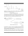
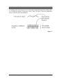
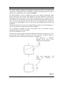
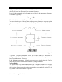
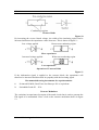
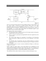
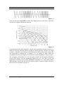
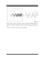
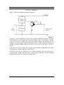
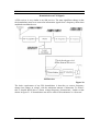
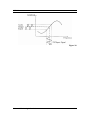
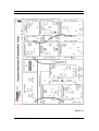
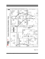
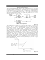
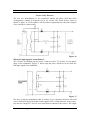
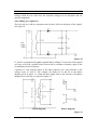
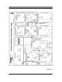
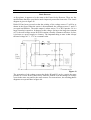
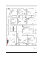
ST2203
Experiment 2
Objective :
Study of Frequency Modulation Using Reactance Modulator
Procedure :
This experiment investigates how ST2203's reactance modulator circuit performs
frequency modulation. This circuit modulates the frequency of a carrier sine wave,
according to the audio signal applied to its modulating output. To avoid unnecessary
loading of monitored signals, X10 Oscilloscope probes should be used throughout this
experiment.
1.
Ensure that the following initial conditions exist on the ST2203 Module.
a. All Switch Faults in ‘Off’ condition.
b. Amplitude potentiometer (in the mixer/amplifier block) in fully clockwise.
c. VCO switch (in phase-locked loop detector block) in ‘Off’ position.
2.
Make the connections as shown in figure 19.
3.
Turn on power to the ST2203 module
4.
Turn the audio oscillator block's amplitude potentiometer to its fully clockwise
(Maximum) positions, and examines the block's output (TP1) on an
Oscilloscope.
This is the audio frequency sine wave, which will be used as our modulating
signal. Note that the sine wave's frequency can be adjusted from about 300 Hz
to approximately 3.4 KHz by adjusting the audio oscillator's frequency
potentiometer Note also that the amplitude of this audio modulating signal can
be reduced to zero, by turning the audio oscillator's amplitude potentiometer to
its fully counter clockwise position.
5.
Connect the output socket of the audio oscillator block to the audio input socket
of the modulator circuit’s block, as shown in figure 19.
6.
Put the reactance /varactor switch in the reactance position. This switches the
output of the reactance modulator through to the input of the mixer/amplifier
block~ and also switches off the varactor modulator block to avoid interference
between the two modulators.
7.
The output signal from the reactance modulator block appears at TP13, before
being buffered and amplified by the mixer/amplifier block. Although the output
from the reactance modulator block can be monitored directly at TP13, any
capacitive loading affect this point (e.g. due to an Oscilloscope probe) may
slightly affect the modulator's output frequency.
In order to avoid this problem we will monitor the buffered FM output signal
from the mixer/amplifier block at TP34.
8.
Put the reactance modulator's potentiometer in its midway position (arrow
pointing towards top of PCB) then examine TP34.
Scientech Technologies Pvt. Ltd.
22