1
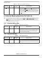
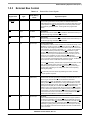
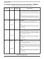
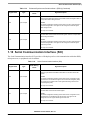
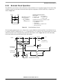
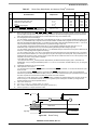
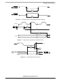
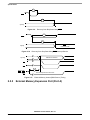
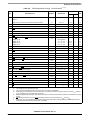
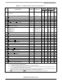
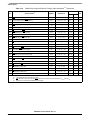
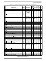
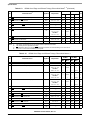
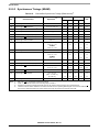
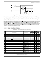
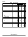
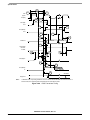
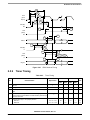
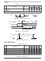
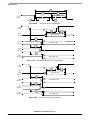
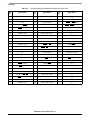
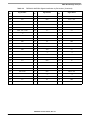
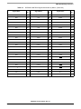
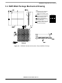
Specifications
Table 2-5.
Clock Operation
80 MHz
No.
Characteristics
100 MHz
Symbol
Min
Max
Min
Max
Ef
0
80.0 MHz
0
100.0 MHz
1
Frequency of EXTAL (EXTAL Pin Frequency)
The rise and fall time of this external clock should be 3 ns maximum.
2
EXTAL input high1, 2
• With PLL disabled (46.7%–53.3% duty cycle6)
• With PLL enabled (42.5%–57.5% duty cycle6)
ETH
5.84 ns
5.31 ns
∞
157.0 μs
4.67 ns
4.25 ns
∞
157.0 μs
EXTAL input low1, 2
• With PLL disabled (46.7%–53.3% duty cycle6)
• With PLL enabled (42.5%–57.5% duty cycle6)
ETL
5.84 ns
5.31 ns
∞
157.0 μs
4.67 ns
4.25 ns
∞
157.0 μs
EXTAL cycle time2
• With PLL disabled
• With PLL enabled
ETC
12.50 ns
12.50 ns
∞
273.1 μs
10.00 ns
10.00 ns
∞
273.1 μs
3
4
5
CLKOUT change from EXTAL fall with PLL disabled
4.3 ns
11.0 ns
4.3 ns
11.0 ns
6
a. CLKOUT rising edge from EXTAL rising edge with PLL enabled (MF
= 1 or 2 or 4, PDF = 1, Ef > 15 MHz)3,5
0.0 ns
1.8 ns
0.0 ns
1.8 ns
b. CLKOUT falling edge from EXTAL falling edge with PLL enabled (MF
≤ 4, PDF ≠ 1, Ef / PDF > 15 MHz)3,5
0.0 ns
1.8 ns
0.0 ns
1.8 ns
25.0 ns
12.50 ns
∞
8.53 μs
20.0 ns
10.00 ns
∞
8.53 μs
Instruction cycle time = ICYC = TC4
(see Table 2-4) (46.7%–53.3% duty cycle)
• With PLL disabled
• With PLL enabled
7
Notes:
1.
2.
3.
4.
5.
6.
2.5.3
ICYC
Measured at 50 percent of the input transition
The maximum value for PLL enabled is given for minimum VCO frequency (see Table 2-6) and maximum MF.
Periodically sampled and not 100 percent tested
The maximum value for PLL enabled is given for minimum VCO frequency and maximum DF.
The skew is not guaranteed for any other MF value.
The indicated duty cycle is for the specified maximum frequency for which a part is rated. The minimum clock high or low time
required for correction operation, however, remains the same at lower operating frequencies; therefore, when a lower clock
frequency is used, the signal symmetry may vary from the specified duty cycle as long as the minimum high time and low time
requirements are met.
Phase Lock Loop (PLL) Characteristics
Table 2-6.
PLL Characteristics
80 MHz
100 MHz
Characteristics
Unit
Voltage Controlled Oscillator (VCO) frequency when PLL
enabled (MF × Ef × 2/PDF)
PLL external capacitor (PCAP pin to VCCP) (CPCAP)
• @ MF ≤ 4
•
@ MF > 4
Note:
Min
Max
Min
Max
30
160
30
200
MHz
(MF × 580) −
100
MF × 830
(MF × 780) −
140
MF × 1470
(MF × 580) − 100
(MF × 780) − 140
pF
MF × 830
MF × 1470
pF
CPCAP is the value of the PLL capacitor (connected between the PCAP pin and VCCP). The recommended value in pF for CPCAP
can be computed from one of the following equations:
(680 × MF) – 120, for MF ≤ 4, or
1100 × MF, for MF > 4.
DSP56301 Technical Data, Rev. 10
2-6
Freescale Semiconductor