1
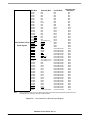
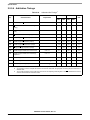
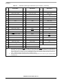
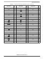
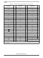
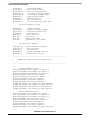
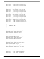
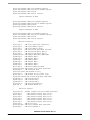
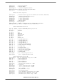
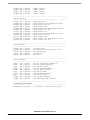
AC Electrical Characteristics
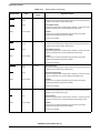
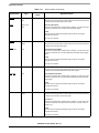
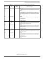
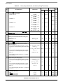
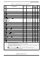
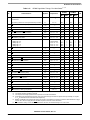
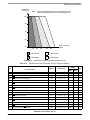
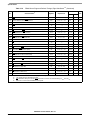
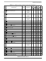
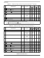
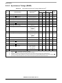
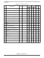
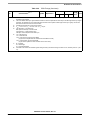
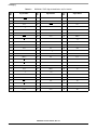
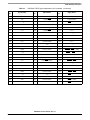
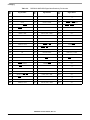
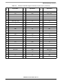
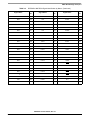
Table 2-22.
Characteristics4, 5, 7
No.
ESSI Timings (Continued)
80 MHz
Symbol
Min
Notes:
1.
2.
3.
4.
5.
6.
7.
8.
100 MHz
Expression
Max
Min
Max
CondUnit
ition6
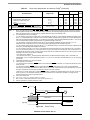
For the internal clock, the external clock cycle is defined by the instruction cycle time (timing 7 in Table 2-5 on page 2-6) and
the ESSI control register.
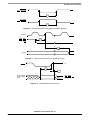
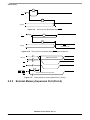
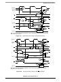
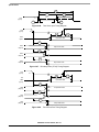
The word-relative frame sync signal waveform relative to the clock operates the same way as the bit-length frame sync signal
waveform, but spreads from one serial clock before the first bit clock (same as Bit Length Frame Sync signal), until the one
before the last bit clock of the first word in frame.
Periodically sampled and not 100 percent tested
VCC = 3.3 V ± 0.3 V; TJ = −40°C to +100 °C, CL = 50 pF
TXC (SCK Pin) = Transmit Clock
RXC (SC0 or SCK Pin) = Receive Clock
FST (SC2 Pin) = Transmit Frame Sync
FSR (SC1 or SC2 Pin) Receive Frame Sync
i ck = Internal Clock
x ck = External Clock
i ck a = Internal Clock, Asynchronous Mode
(Asynchronous implies that TXC and RXC are two different clocks)
i ck s = Internal Clock, Synchronous Mode
(Synchronous implies that TXC and RXC are the same clock)
bl = bit length
wl = word length
wr = word length relative
If the DSP core writes to the transmit register during the last cycle before causing an underrun error, the delay is 20 ns + (0.5 ×
TC).
DSP56301 Technical Data, Rev. 10
Freescale Semiconductor
2-45