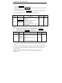
1
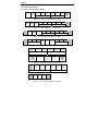
CHF Series Universal Inverter
Operation Manual
z
Thank you very much for your buying CHF series universal inverter.
z
Before use, please read this manual thoroughly to ensure proper usage. Keep this
manual at an easily accessible place so that can refer anytime as necessary.
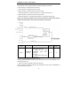
Safety Precautions
Please read this operation manual carefully before installation, operation, maintenance or
inspection.
In this manual, the safety precautions were sorted to “WARNING” or “CAUTION”.
WARNING
CAUTION
Indicates a potentially dangerous situation which, if can not
avoid will result in death or serious injury.
Indicates a potentially dangerous situation which, if can not
avoid will cause minor or moderate injury and damage the
device. This
Symbol is also used for warning any un-safety operation.
In some cases, even the contents of “CAUTION” still can cause serious accident.
Please follow these important precautions in any situation.
★ NOTE indicate the necessary operation to ensure the device run properly.
Warning Marks are placed on the front cover of the inverter.
Please follow these indications when using the inverter.
WARNING
z
May cause injury or electric shock.
z
Please follow the instructions in the manual before installation or operation.
z
Disconnect all power line before opening front cover of unit. Wait at least 1
minute until DC Bus capacitors discharge.
z
Use proper grounding techniques.
z
Never connect AC power with UVW terminals
I
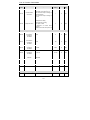
TABLE OF CONTENTS
TABLE OF CONTENTS ............................................................................................ II
LIST OF FIGURES ...................................................................................................IV
1. INTRODUCTION................................................................................................. 1
1.1 Technology Features .................................................................................... 1
1.2 Description of Name Plate ........................................................................... 2
1.3 Selection Guide ............................................................................................ 2
1.4 Parts Description .......................................................................................... 5
1.5 External Dimension ...................................................................................... 6
2. INSPECTION ...................................................................................................... 8
3. INSTALLATION................................................................................................... 9
3.1 Environmental Requirement....................................................................... 10
3.2 Installation Space ........................................................................................11
3.3 Dimensions of External Keypad ................................................................. 12
3.4 Disassembly ............................................................................................... 12
4. WIRING ............................................................................................................. 14
4.1 Connection of Peripheral Devices.............................................................. 15
4.2 Terminal Configuration ............................................................................... 16
4.2.1 Main Circuit Terminals ..................................................................... 16
4.2.2 Control Circuit Terminals ................................................................. 17
4.3 Typical Wiring Diagram .............................................................................. 18
4.4 Specifications of Breaker, Cable, Contactor and Reactor.......................... 19
4.4.1 Specifications of breaker, cable and contactor................................ 19
4.4.2 Specifications of AC input/output reactor and DC reactor............... 20
4.4.3 Specifications of braking resistor..................................................... 21
4.5 Wiring Main Circuits ................................................................................... 23
4.5.1 Wiring at input side of main circuit ................................................ 23
4.5.2 Wiring at inverter side of main circuit............................................ 23
4.5.3 Wiring at motor side of main circuit............................................. 24
4.5.4 Wiring of regenerative unit .......................................................... 24
4.5.5 Wiring of Common DC bus.............................................................. 25
4.5.6 Ground Wiring (PE) ......................................................................... 26
4.6 Wiring Control Circuit ................................................................................. 26
4.6.1 Precautions...................................................................................... 26
4.6.2 Control circuit terminals ................................................................... 26
4.6.3 Jumper on control board.................................................................. 27
4.7 Installation Guidline to EMC Compliance................................................... 28
4.7.1 General knowledge of EMC ............................................................ 28
4.7.2 EMC features of inverter.................................................................. 28
4.7.3 EMC Installation Guideline .............................................................. 29
5.
OPERATION.................................................................................................... 31
5.1 Keypad Description .................................................................................... 31
5.1.1 Keypad schematic diagram ............................................................. 31
5.1.2 Function key description.................................................................. 31
5.1.3 Indicator light description................................................................. 32
II
5.2 Operation Process ......................................................................................33
5.2.1 Parameter setting............................................................................ 33
5.2.2 Fault reset ....................................................................................... 34
5.2.3 Motor parameters autotuning.......................................................... 34
5.2.4 Password setting............................................................................. 34
5.2.5 Shortcut menu setting ..................................................................... 34
5.3 Running State .............................................................................................35
5.3.1 Power-on initialization ..................................................................... 35
5.3.2 Stand-by .......................................................................................... 35
5.3.3 Motor parameters autotuning.......................................................... 35
5.3.4 Operation ........................................................................................ 35
5.3.5 Fault ................................................................................................ 35
5.4 Shortcut Menu.............................................................................................36
5.4.1 Shortcut menu operation................................................................. 36
5.4.2 Quick debugging mode ................................................................... 37
6. DETAILED FUNCTION DESCRIPTION............................................................39
6.1 P0 Group--Basic Function ..........................................................................39
6.2 P1 Group --Start and Stop Control..............................................................45
6.3 P2 Group--Motor Parameters...................................................................49
6.4 P3 Group—Frequency Setting....................................................................50
6.5 P4 Group—V/F Control...............................................................................54
6.6 P5 Group--Input Terminals..........................................................................56
6.7 P6 Group--Output Terminals.......................................................................64
6.8 P7 Group—Display Interface ......................................................................67
6.9 P8 Group--Enhanced Function ...................................................................72
6.10 P9 Group--PID Control .............................................................................78
6.11 PA Group--Simple PLC and Multi-steps Speed Control............................82
6.12 PB Group-- Protection Function ...............................................................88
6.13 PC Group--Serial Communication ............................................................91
6.14 PD Group--Supplementary Function ........................................................93
6.15 PE Group—Factory Setting ......................................................................94
7. TROUBLE SHOOTING........................................................................................95
7.1 Fault and Trouble shooting .........................................................................95
7.2 Common Faults and Solutions....................................................................97
8.
MAINTENANCE...............................................................................................98
8.1 Daily Maintenance ......................................................................................98
8.2 Periodic Maintenance .................................................................................99
8.3 Replacement of wearing parts ....................................................................99
9.
LIST OF FUNCTION PARAMETERS............................................................101
10. COMMUNICATION PROTOCOL..................................................................... 119
III
LIST OF FIGURES
Figure 1.1
Nameplate of inverter. ................................................................................. 2
Figure 1.2
Parts of inverter (15kw and below). ............................................................. 5
Figure 1.3
Parts of inverter (18.5kw and above)........................................................... 6
Figure1.4
Dimensions (15kW and below). .................................................................... 6
Figure 1.5
Dimensions (18.5 ~110kW). ........................................................................ 6
Figure 1.6
Dimensions (132~315kW). .......................................................................... 6
Figure 1.7
Dimensions (350~630kW). .......................................................................... 7
Figure 3.1
Relationship between output current and altitude. .................................... 10
Figure 3.2
Safety space. ............................................................................................. 11
Figure 3.3
Installation of multiple inverters. ................................................................ 11
Figure 3.4
Dimension of small keypad........................................................................ 12
Figure 3.5
Dimension of big keypad. .......................................................................... 12
Figure 3.6
Disassembly of plastic cover. .................................................................... 12
Figure 3.7
Disassembly of metal plate cover.............................................................. 13
Figure 3.8
Open inverter cabinet. ............................................................................... 13
Figure 4.1
Connection of peripheral devices. ............................................................. 15
Figure 4.2
Main circuit terminals (1.5~2.2kW). ........................................................... 16
Figure 4.3
Main circuit terminals (4~5.5kW). .............................................................. 16
Figure 4.4
Main circuit terminals (7.5~15kW). ............................................................ 16
Figure 4.5
Main circuit terminals (18.5~110kW). ........................................................ 16
Figure 4.6
Main circuit terminals (132~315kW). ......................................................... 16
Figure 4.7
Main circuit terminals (350~630kW). ......................................................... 16
Figure 4.8
Control circuit terminals (1.5~2.2kW). ....................................................... 17
Figure 4.9
Control circuit terminals (4kW and above)................................................. 17
Figure4.10
Wiring diagram. .......................................................................................... 18
Figure4.11
Wiring at input side. .................................................................................. 23
Figure 4.12
Wiring at motor side. ................................................................................. 24
Figure 4.13
Wiring of regenerative unit. ....................................................................... 25
Figure 4.14
Wiring of common DC bus. ....................................................................... 25
Figure 5.1
Keypad schematic diagram. ...................................................................... 31
Figure 5.2
Flow chart of parameter setting. ................................................................ 33
Figure 5.3
Shortcut menu operation. .......................................................................... 36
Figure 6.1
Acceleration and deceleration time. .......................................................... 41
Figure 6.2
Multiple V/F curve diagram. ....................................................................... 42
Figure 6.3
Torque boost diagram. .............................................................................. 42
Figure 6.4
Effect of carrier frequency. ........................................................................ 43
Figure 6.5
Starting diagram. ....................................................................................... 45
IV
Figure 6.6
DC braking diagram................................................................................... 47
Figure 6.7
FWD/REV dead time diagram. .................................................................. 47
Figure 6.8
Reference frequency diagram. .................................................................. 52
Figure 6.9
Skip frequency diagram. ............................................................................ 54
Figure 6.10
V/F curve setting diagram.......................................................................... 56
Figure 6.11
2-wire control mode 1. ............................................................................... 60
Figure 6.12
2-wire control mode 2. ............................................................................... 60
Figure 6.13
3-wire control mode 1. ............................................................................... 61
Figure 6.14
3-wire control mode 2. ............................................................................... 61
Figure 6.15
Relationship between AI and corresponding setting. ................................ 62
Figure 6.16
Relationship between AO and corresponding setting. .............................. 66
Figure 6.17
Relationship between HDO and corresponding setting............................. 67
Figure 6.18
Traverse operation diagram. ..................................................................... 73
Figure 6.19
Timing chart for preset and specified count reached. ............................... 75
Figure 6.20
FDT level and lag diagram. ....................................................................... 75
Figure 6.21
Frequency arriving detection diagram. ...................................................... 76
Figure 6.22
Droop control diagram. .............................................................................. 76
Figure 6.23
Simple water-supply control function diagram........................................... 77
Figure 6.24
PID control diagram................................................................................... 79
Figure 6.25
Reducing overshooting diagram................................................................ 80
Figure 6.26
Rapidly stabilizing diagram........................................................................ 81
Figure 6.27
Reducing long-cycle oscillation diagram. .................................................. 81
Figure 6.28
Reducing short-cycle oscillation diagram. ................................................. 81
Figure 6.29
Relationship between bias limit and output frequency. ............................. 82
Figure 6.30
Simple PLC operation diagram.................................................................. 83
Figure 6.31
Multi-steps speed operation diagram. ....................................................... 85
Figure 6.32
Simple PLC continue from paused step. ................................................... 87
Figure 6.33
Motor overload protection curve. ............................................................... 88
Figure 6.34
Over-voltage stall function. ........................................................................ 89
Figure 6.35
Current limiting protection function. ........................................................... 90
Figure 6.36
Meaning of PC.06...................................................................................... 93
V
Introduction
1.
INTRODUCTION
1.1 Technology Features
● Input & Output
◆Input
Voltage Range:
380/220V±15%
◆Input
Frequency Range:
47~63Hz
◆Output
Voltage Range:
0~rated input voltage
◆Output
Frequency Range:
0~400Hz
● I/O Features
◆ Programmable
Digital Input: Provide 4 terminals which can accept ON-OFF inputs,
and 1 terminal which can accept high speed pulse input.
◆ Programmable
Analog Input: AI1 can accept input of 0 ~10V, AI2 can accept input of
0~10V or 0~20mA.
◆ Programmable
Open Collector Output: Provide 1 output terminal (open collector
output or high speed pulse output)
◆ Relay
Output: Provide 2 output terminals (1 for 2.2kW and below)
◆ Analog
Output: Provide 1 output terminal, whose output scope can be 0/4~20 mA or
0~10 V, as chosen.
● Main Control Function
◆Control Mode: V/F control.
◆Overload
◆Speed
Capacity: 60s with 150% of rated current, 10s with 180% of rated current.
Adjusting Range: 1:100.
◆Carrier
Frequency: 0.5kHz ~15.0kHz.
◆Frequency
reference source: keypad, analog input, HDI, serial communication,
multi-step speed, simple PLC and PID. The combination of multi- modes and the
switch between different modes can be realized.
◆PID
Control Function
◆Simple
PLC, Multi-Steps Speed Control Function: 16 steps speed can be set.
◆ Traverse
Control Function
and Time Control Function
◆ None-Stop when instantaneous power off.
◆Speed Trace Function: Smoothly start the running motor.
◆QUICK/JOG Key: User defined shortcut key can be realized.
◆ Automatic Voltage Regulation Function (AVR):
◆ Length
Automatically keep the output voltage stable when input voltage fluctuating
◆ Up
to 23 fault protections:
Protect from over current, over voltage, under voltage, over temperature, phase failure,
over load etc.
1
Introduction
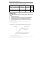
1.2 Description of Name Plate
Figure 1.1
Nameplate of inverter.
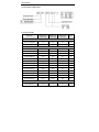
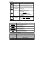
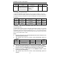
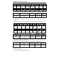
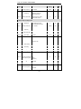
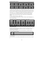
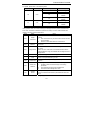
1.3 Selection Guide
Rated output
Power (kW)
Rated input
current (A)
Rated output
current (A)
Size
CHF100-1R5G-S2
1.5
14.2
7.0
B
CHF100-2R2G-S2
2.2
23.0
10
B
CHF100-0R7G-2
0.75
5.0
4.5
B
CHF100-1R5G-2
1.5
7.7
7
B
CHF100-2R2G-2
2.2
11.0
10
B
CHF100-004G-2
4.0
17.0
16
C
CHF100-5R5G-2
5.5
21.0
20
C
CHF100-7R5G-2
7.5
31.0
30
D
Model No.
1AC 220V ±15%
3AC 220V ±15%
CHF100-011G-2
11.0
43.0
42
E
CHF100-015G-2
15.0
56.0
55
E
CHF100-018G-2
18.5
71.0
70
E
CHF100-022G-2
22.0
81.0
80
F
CHF100-030G-2
30.0
112.0
110
F
CHF100-037G-2
37.0
132.0
130
F
CHF100-045G-2
45.0
163.0
160
G
0.75
3.4
2.5
B
3AC 380V ±15%
CHF100-0R7G-4
2
Introduction
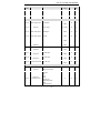
CHF100-1R5G-4
1.5
5.0
3.7
B
CHF100-2R2G-4
2.2
5.8
5
B
CHF100-004G/5R5P-4
4.0/5.5
10/15
9/13
C
CHF100-5R5G/7R5P-4
5.5/7.5
15/20
13/17
C
CHF100-7R5G/011P-4
7.5/11
20/26
17/25
D
CHF100-011G/015P-4
11/15
26/35
25/32
D
CHF100-015G/018P-4
15/ 18.5
35/38
32/37
D
CHF100-018G/022P-4
18.5/ 22
38/46
37/45
E
CHF100-022G/030P-4
22/30
46/62
45/60
E
CHF100-030G/037P-4
30/37
62/76
60/75
E
CHF100-037G/045P-4
37/45
76/90
75/90
F
CHF100-045G/055P-4
45/55
90/105
90/110
F
CHF100-055G/075P-4
55/75
105/ 140
110/ 150
F
CHF100-075G/090P-4
75/90
140/ 160
150/ 176
G
CHF100-090G/110P-4
90/110
160/ 210
176/ 210
G
CHF100-110G/132P-4
110/132
210/ 240
210/ 250
G
CHF100-132G/160P-4
132/160
240/ 290
250/ 300
H
CHF100-160G/185P-4
160/185
290/ 330
300/ 340
H
CHF100-185G/200P-4
185/200
330/ 370
340/ 380
H
CHF100-200G/220P-4
200/220
370/ 410
380/ 415
I
CHF100-220G/250P-4
220/250
410/ 460
415/ 470
I
CHF100-250G/280P-4
250/280
460/ 500
470/ 520
I
CHF100-280G/315P-4
280/315
500/ 580
520/ 600
I
CHF100-315G/350P-4
315/350
580/ 620
600/ 640
I
CHF100-350G-4
350
620
640
2*H
CHF100-400G-4
400
670
690
2*I
CHF100-500G-4
500
835
860
2*I
CHF100-560G-4
560
920
950
2*I
CHF100-630G-4
630
1050
1100
2*I
CHF100-710G-4
710
1250
1300
3*I
CHF100-800G-4
800
1450
1520
3*I
3AC 690V ±15%
3
Introduction
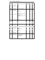
CHF100-022G-6
CHF100-030G-6
CHF100-037G-6
CHF100-045G-6
CHF100-055G-6
CHF100-075G-6
CHF100-090G-6
CHF100-110G-6
CHF100-132G-6
CHF100-160G-6
CHF100-185G-6
CHF100-200G-6
CHF100-220G-6
CHF100-250G-6
CHF100-280G-6
CHF100-315G-6
CHF100-350G-6
CHF100-400G-6
CHF100-500G-6
CHF100-560G-6
CHF100-630G-6
22
30
37
45
55
75
90
110
132
160
185
200
220
250
280
315
350
400
500
560
630
35
40
47
52
65
85
95
118
145
165
190
210
230
255
285
334
360
411
518
578
655
4
28
35
45
52
63
86
98
121
150
175
198
218
240
270
300
350
380
430
540
600
680
E
E
F
F
F
F
G
G
G
H
H
H
I
I
I
I
I
I
2*I
2*I
2*I
Introduction
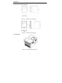
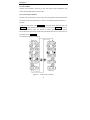
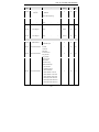
1.4 Parts Description
Figure 1.2
Parts of inverter (15kw and below).
5
Introduction
Figure 1.3
Parts of inverter (18.5kw and above).
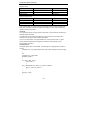
1.5 External Dimension
Figure1.4
Dimensions (15kW and below).
Figure 1.6
Figure 1.5
Dimensions (18.5 ~110kW).
Dimensions (132~315kW).
6
Introduction
Figure 1.7
A
(mm)
Dimensions (350~630kW).
B
(mm)
H
(mm)
W
(mm)
D
(mm)
Power
(kW)
Size
0.75~2.2
B
110.4
170.2
180
120
140
Installation
Dimension
External Dimension
Installation
Hole
(mm)
5
4~5.5
C
147.5
237.5
250
160
175
5
7.5~15
D
206
305.5
320
220
180
6.0
18.5~30
E
176
454.5
467
290
215
6.5
37~55
F
230
564.5
577
375
270
7.0
75~110
G
H(without
base)
H(with base)
I(without
base)
I(with base)
320
738.5
755
460
330
9.0
270
1233
1275
490
391
13.0
132~185
200~315
350~630
—
—
1490
490
391
—
500
1324
1358
750
402
12.5
—
—
1670
750
402
—
J(with base)
See Figure 1.7
7
Inspection
2.
INSPECTION
CAUTION
● Don’t install or use any inverter that is damaged or have fault part, otherwise
may cause injury.
Check the following items when unpacking the inverter,
1. Inspect the entire exterior of the Inverter to ensure there are no scratches or
other damage caused by the transportation.
2. Ensure there is operation manual and warranty card in the packing box.
3. Inspect the nameplate and ensure it is what you ordered.
4. Ensure the optional parts are what you need if have ordered any optional parts.
Please contact the local agent if there is any damage in the inverter or optional parts.
8
Installation
3.
INSTALLATION
WARNING
●
The person without passing the training manipulate the device or any rule in the
“Warning” being violated, will cause severe injury or property loss. Only the person,
who has passed the training on the design, installation, commissioning and
operation of the device and gotten the certification, is permitted to operate this
equipment.
● Input power cable must be connected tightly, and the equipment must be grounded
securely.
● Even if the inverter is not running, the following terminals still have dangerous
voltage:
- Power Terminals: R, S, T
- Motor Connection Terminals: U, V, W.
● When power off, should not install the inverter until 5 minutes after, which will ensure
the device discharge completely.
● The section area of grounding conductor must be no less than that of power supply
cable.
CAUTION
●When moving the inverter please lift by its base and don’t lift by the panel. Otherwise
may cause the main unit fall off which may result in personal injury.
● Install the inverter on the fireproofing material (such as metal) to prevent fire.
● When need install two or more inverters in one cabinet, cooling fan should be
provided to make sure that the air temperature is lower than 45°C. Otherwise it could
cause fire or damage the device.
9
Installation
3.1 Environmental Requirement
3.1.1
Temperature
Environment temperature range: -10°C ~ +40°C. Inverter will be derated if ambient
temperature exceeds 40°C.
3.1.2
Humidity
Less than 95% RH, without dewfall.
3.1.3
Altitude
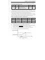
Inverter can output the rated power when installed with altitude of lower than 1000m. It
will be derated when the altitude is higher than 1000m. For details, please refer to the
following figure:
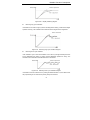
(m)
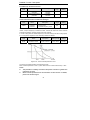
Figure 3.1
3.1.4
Relationship between output current and altitude.
Impact and Oscillation
It is not allowed that the inverter falls down or suffers from fierce impact or the inverter
installed at the place that oscillation frequently.
3.1.5
Electromagnetic Radiation
Keep away from the electromagnetic radiation source.
3.1.6
Water
Do not install the inverter at the wringing or dewfall place.
3.1.7
Air Pollution
Keep away from air pollution such as dusty, corrosive gas.
3.1.8
Storage
Do not store the inverter in the environment with direct sunlight, vapor, oil fog and
vibration.
10
Installation
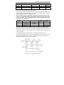
3.2 Installation Space
Figure 3.2
Figure 3.3
Safety space.
Installation of multiple inverters.
Notice: Add the air deflector when apply the up-down installation.
11
Installation
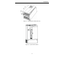
3.3 Dimensions of External Keypad
Figure 3.4
Figure 3.5
Dimension of small keypad.
Dimension of big keypad.
3.4 Disassembly
Figure 3.6
Disassembly of plastic cover.
12
Installation
Figure 3.7
Disassembly of metal plate cover.
Figure 3.8
Open inverter cabinet.
13
Wiring
4.
WIRING
WARNING
● Wiring must be performed by the person certified in electrical work.
● Forbid testing the insulation of cable that connects the inverter with high-voltage
insulation testing devices.
● Cannot install the inverter until discharged completely after the power supply is
switched off for 5 minutes.
● Be sure to ground the ground terminal.
(200V class: Ground resistance should be 100Ω or less, 400V class: Ground
resistance should be 10Ω or less, 660V class: Ground resistance should be 5Ω or
less). Otherwise, it might cause electric shock or fire.
● Connect input terminals (R, S, T) and output terminals (U, V, W) correctly.
Otherwise it will cause damage the inside part of inverter.
● Do not wire and operate the inverter with wet hands.
Otherwise there is a risk of electric shock.
CAUTION
●Check
to be sure that the voltage of the main AC power supply satisfies the rated
voltage of the Inverter.
Injury or fire can occur if the voltage is not correct.
● Connect power supply cables and motor cables tightly.
14
Wiring
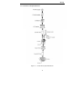
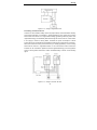
4.1 Connection of Peripheral Devices
Figure 4.1
Connection of peripheral devices.
15
Wiring
4.2 Terminal Configuration
4.2.1 Main Circuit Terminals (380VAC)
(+)
R
PB
S
PB
R
(-)
PB
S
R
U
MOTOR
S
P1
T
(+)
T
V
W
MOTOR
(-)
U
V
W
MOTOR
U
V
POWER
Figure 4.6
R
(+)
(-)
Main circuit terminals (132~315kW).
S
T
POWER
(+)
W
MOTOR
P1
Figure 4.7
U
Main circuit terminals (18.5~110kW).
S
P1
W
Main circuit terminals (7.5~15kW).
POWER
Figure 4.5
V
POWER
T
R
T
Main circuit terminals (4~5.5kW).
(-)
S
W
MOTOR
POWER
Figure 4.4
R
V
Main circuit terminals (1.5~2.2kW).
Figure 4.3
(+)
U
POWER
Figure 4.2
(+)
T
U
V
MOTOR
(-)
Main circuit terminals (350~630kW).
16
W
Wiring
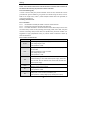
Main circuit terminal functions are summarized according to the terminal symbols in the
following table. Wire the terminal correctly for the desired purposes.
Terminal Symbol
Function Description
R、S、T
Terminals of 3 phase AC input
(+)、(-)
Spare terminals of external braking unit
(+)、PB
Spare terminals of external braking resistor
P1、(+)
Spare terminals of external DC reactor
(-)
Terminal of negative DC bus
U、V、W
Terminals of 3 phase AC output
Terminal of ground
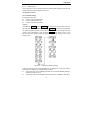
4.2.2 Control Circuit Terminals
485+
485-
+10V
S1
S2
S3
S4
HDI
AI1
AI2
GND
AO
COM
HDO
PW
+24V
Figure 4.8
ROA
ROB
ROC
Control circuit terminals (1.5~2.2kW).
485+
485-
+10V
S1
S2
S3
S4
HDI
AI1
AI2
GND
AO
COM
HDO
PW
+24V
Figure 4.9
ROA
RO1A
RO2B
Control circuit terminals (4kW and above).
17
RO1A
RO2C
RO1C
RO2C
Wiring
4.3 Typical Wiring Diagram
Figure4. 10
Wiring diagram.
Notice:
z
Inverters between 18.5KW and 90KW have built-in DC reactor which is used
to improve power factor. For inverters above 110KW, it is recommended to
install DC reactor between P1 and (+).
z
The inverters below 18.5KW have build-in braking unit. If need braking, only
need to install braking resistor between PB and (+).
z
For inverters above (including) 18.5KW, if need braking, should install
external braking unit between (+) and (-).
z
Only the inverters above 4 KW provide Relay output 2.
z
+24V connect with PW as default setting. If user need external power supply,
disconnect +24V with PW and connect PW with external power supply.
z
485+ and 485- are optional for 485 communications.
18
Wiring
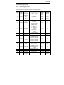
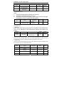
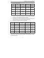
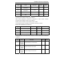
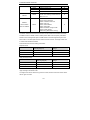
4.4 Specifications of Breaker, Cable, Contactor and Reactor
4.4.1 Specifications of breaker, cable and contactor
Circuit Breaker
(A)
Input/Output Cable
2
(mm )
AC Contactor
(A)
CHF100-1R5G-S2
20
4
16
CHF100-2R2G-S2
32
6
20
3AC 220V ±15%
CHF100-0R4G-2
16
2.5
10
CHF100-0R7G-2
16
2.5
10
CHF100-1R5G-2
20
4
16
CHF100-2R2G-2
32
6
20
CHF100-004G-2
40
6
25
CHF100-5R5G-2
63
6
32
Model No.
1AC 220V ±15%
CHF100-7R5G-2
100
10
63
CHF100-011G-2
125
25
95
CHF100-015G-2
160
25
120
CHF100-018G-2
160
25
120
CHF100-022G-2
200
35
170
CHF100-030G-2
200
35
170
CHF100-037G-2
200
35
170
CHF100-045G-2
250
70
230
CHF100-0R7G-4
10
2.5
10
CHF100-1R5G-4
16
2.5
10
CHF100-2R2G-4
16
2.5
10
CHF100-004G/5R5P-4
25
4
16
CHF100-5R5G/7R5P-4
25
4
16
CHF100-7R5G/011P-4
40
6
25
CHF100-011G/015P-4
63
6
32
3AC 380V ±15%
CHF100-015G/018P-4
63
6
50
CHF100-018G/022P-4
100
10
63
CHF100-022G/030P-4
100
16
80
CHF100-030G/037P-4
125
25
95
CHF100-037G/045P-4
160
25
120
CHF100-045G/055P-4
200
35
135
CHF100-055G/075P-4
200
35
170
19
Wiring
CHF100-075G/090P-4
250
70
230
CHF100-090G/110P-4
315
70
280
CHF100-110G/132P-4
400
95
315
CHF100-132G/160P-4
400
150
380
CHF100-160G/185P-4
630
185
450
CHF100-185G/200P-4
630
185
500
CHF100-200G/220P-4
630
240
580
CHF100-220G/250P-4
800
150x2
630
CHF100-250G/280P-4
800
150x2
700
CHF100-280G/315P-4
1000
185x2
780
CHF100-315G/350P-4
1200
240x2
900
4.4.2 Specifications of AC input/output reactor and DC reactor
Model No.
AC Input reactor
Current Inductance
(A)
(mH)
AC Output reactor
DC reactor
Current Inductance Current Inductance
(A)
(mH)
(A)
(mH)
CHF100-0R7G-4
-
-
-
-
-
-
CHF100-1R5G-4
5
3.8
5
1.5
-
-
CHF100-2R2G-4
7
2.5
7
1
-
-
CHF100-004G/5R5P-4
10
1.5
10
0.6
-
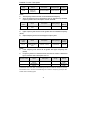
-
CHF100-5R5G/7R5P-4
15
1.4
15
0.25
-
-
CHF100-7R5G/011P-4
20
1
20
0.13
-
-
CHF100-011G/015P-4
30
0.6
30
0.087
-
-
CHF100-015G/018P-4
40
0.6
40
0.066
-
-
CHF100-018G/022P-4
50
0.35
50
0.052
40
1.3
CHF100-022G/030P-4
60
0.28
60
0.045
50
1.08
CHF100-030G/037P-4
80
0.19
80
0.032
65
0.8
CHF100-037G/045P-4
90
0.19
90
0.03
78
0.7
CHF100-045G/055P-4
120
0.13
120
0.023
95
0.54
CHF100-055G/075P-4
150
0.11
150
0.019
115
0.45
CHF100-075G/090P-4
200
0.12
200
0.014
160
0.36
CHF100-090G/110P-4
250
0.06
250
0.011
180
0.33
CHF100-110G/132P-4
250
0.06
250
0.011
250
0.26
20
Wiring
CHF100-132G/160P-4
290
0.04
290
0.008
250
0.26
CHF100-160G/185P-4
330
0.04
330
0.008
340
0.18
CHF100-185G/200P-4
400
0.04
400
0.005
460
0.12
CHF100-200G/220P-4
490
0.03
490
0.004
460
0.12
CHF100-220G/250P-4
490
0.03
490
0.004
460
0.12
CHF100-250G/280P-4
530
0.04
530
0.005
650
0.11
CHF100-280G/315P-4
600
0.04
600
0.005
650
0.11
CHF100-315G/350P-4
660
0.02
660
0.002
800
0.06
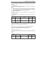
4.4.3 Specifications of braking unit and braking resistor
Model No.
Braking unit
Order No.
Braking resistor
Quantity
Specification
Quantity
CHF100-0R4G-2
275Ω/75W
1
CHF100-0R7G-2
275Ω/75W
1
130Ω/260W
1
CHF100-2R2G-2
80Ω/260W
1
CHF100-004G-2
48Ω/400W
1
CHF100-5R5G-2
35Ω/550W
1
CHF100-7R5G-2
26Ω/780W
1
CHF100-011G-2
17Ω/1100W
1
13Ω/1800W
1
CHF100-018G-2
10Ω/2200W
1
CHF100-022G-2
8Ω/2500W
1
CHF100-030G-2
13Ω/1800W
2
10Ω/2200W
2
8Ω/2500W
2
3AC 220V ±15%
CHF100-1R5G-2
CHF100-015G-2
CHF100-037G-2
Built-in
1
DBU-055-2
1
DBU-055-2
2
CHF100-045G-2
3AC 380V±15%
CHF100-0R7G-4
Built-in
1
CHF100-1R5G-4
CHF100-2R2G-4
CHF100-004G/5R5P-4
21
900Ω/75W
1
400Ω/260W
1
150Ω/390W
1
Wiring
CHF100-5R5G/7R5P-4
CHF100-7R5G/011P-4
CHF100-011G/015P-4
CHF100-015G/018P-4
100Ω/520W
1
50Ω/1040W
1
40Ω/1560W
1
20Ω/6000W
1
13.6Ω/9600W
1
CHF100-018G/022P-4
CHF100-022G/030P-4
CHF100-030G/037P-4
CHF100-037G/045P-4
DBU-055-4
1
CHF100-045G/055P-4
CHF100-055G/075P-4
CHF100-075G/090P-4
CHF100-090G/110P-4
DBU-055-4
2
13.6Ω/9600W
2
DBU-160-4
1
4Ω/30000W
1
DBU-220-4
1
3Ω/40000W
1
DBU-315-4
1
3Ω/40000W
2
CHF100-110G/132P-4
CHF100-132G/160P-4
CHF100-160G/185P-4
CHF100-185G/200P-4
CHF100-200G/220P-4
CHF100-220G/250P-4
CHF100-250G/280P-4
CHF100-280G/315P-4
CHF100-315G/350P-4
Notice:
1.
Above selection is based on following condition:
100% braking torque, 10% usage rate.
2.
Brake threshold voltage: 700V (380V inverter), 370V (220V inverter)
3.
Parallel connection of braking unit is helpful to improve braking capability.
4.
Wire between inverter and braking unit should be less than 5m.
5.
Wire between braking unit and braking resistor should be less than 10m.
6.
Braking unit can be used for braking continuously for 5 minutes. When braking
unit is working, temperature of cabinet will be high, user is not allowed to touch to
prevent from injure.
For more details, please refer to DBU and RBU user manual.
22
Wiring
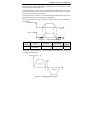
4.5 Wiring Main Circuits
4.5.1
4.5.1.1
Wiring at input side of main circuit
Circuit breaker
It is necessary to connect a circuit breaker which is compatible with the capacity of
inverter between 3ph AC power supply and power input terminals (R, S, T ). The capacity
of breaker is 1.5~2 times to the rated current of inverter. For details, see <Specifications
of Breaker, Cable, and Contactor>.
4.5.1.2
Contactor
In order to cut off the input power effectively when something is wrong in the system,
contactor should be installed at the input side to control the ON-OFF of the main circuit
power supply.
4.5.1.3
AC reactor
In order to prevent the rectifier damage result from the large current, AC reactor should
be installed at the input side. It can also prevent rectifier from sudden variation of power
voltage or harmonic generated by phase-control load.
4.5.1.4
Input EMC filter
The surrounding device may be disturbed by the cables when the inverter is working.
EMC filter can minimize the interference. Just like the following figure.
Figure4.11
4.5.2
4.5.2.1
Wiring at input side.
Wiring at inverter side of main circuit
DC reactor
Inverters from 18.5kW to 90kW have built-in DC reactor which can improve the power
factor,
4.5.2.2
Braking unit and braking resistor
23
Wiring
• Inverter of 15KW and below have built-in braking unit. In order to dissipate the
regenerative energy generated by dynamic braking, the braking resistor should be
installed at (+) and PB terminals. The wire length of the braking resistor should be less
than 5m.
• Inverter of 18.5KW and above need connect external braking unit which should be
installed at (+) and (-) terminals. The cable between inverter and braking unit should be
less than 5m. The cable between braking unit and braking resistor should be less than
10m.
• The temperature of braking resistor will increase because the regenerative energy will
be transformed to heat. Safety protection and good ventilation is recommended.
Notice: Be sure that the electric polarity of (+) (-) terminals is right; it is not allowed
to connect (+) with (-) terminals directly, Otherwise damage or fire could occur.
4.5.3
4.5.3.1
Wiring at motor side of main circuit
Output Reactor
When the distance between inverter and motor is more than 50m, inverter may be tripped
by over-current protection frequently because of the large leakage current resulted from
the parasitic capacitance with ground. And the same time to avoid the damage of motor
insulation, the output reactor should be installed.
4.5.3.2
Output EMC filter
EMC filter should be installed to minimize the leakage current caused by the cable and
minimize the radio noise caused by the cables between the inverter and cable. Just see
the following figure.
Figure 4.12
4.5.4
Wiring at motor side.
Wiring of regenerative unit
Regenerative unit is used for putting the electricity generated by braking of motor to the
grid. Compared with traditional 3 phase inverse parallel bridge type rectifier unit,
regenerative unit uses IGBT so that the total harmonic distortion (THD) is less than 4%.
Regenerative unit is widely used for centrifugal and hoisting equipment.
24
Wiring
Figure 4.13
Wiring of regenerative unit.
4.5.5 Wiring of Common DC bus
Common DC bus method is widely used in the paper industry and chemical fiber industry
which need multi-motor to coordinate. In these applications, some motors are in driving
status while some others are in regenerative braking (generating electricity) status. The
regenerated energy is automatically balanced through the common DC bus, which means
it can supply to motors in driving status. Therefore the power consumption of whole
system will be less compared with the traditional method (one inverter drives one motor).
When two motors are running at the same time (i.e. winding application), one is in driving
status and the other is in regenerative status. In this case the DC buses of these two
inverters can be connected in parallel so that the regenerated energy can be supplied to
motors in driving status whenever it needs. Its detailed wiring is shown in the following
figure:
Figure 4.14
Wiring of common DC bus.
25
Wiring
Notice: Two inverters must be the same model when connected with Common DC
bus method. Be sure they are powered on at the same time.
4.5.6 Ground Wiring (PE)
In order to ensure safety and prevent electrical shock and fire, terminal PE must be
grounded with ground resistance. The ground wire should be big and short, and it is
2
better to use copper wire (>3.5mm ). When multiple inverters need to be grounded, do
not loop the ground wire.
4.6 Wiring Control Circuit
4.6.1 Precautions
4.6.1.1
Use shielded or twisted-pair cables to connect control terminals.
4.6.1.2
Connect the ground terminal (PE) with shield wire.
4.6.1.3
The cable connected to the control terminal should leave away from the main
circuit and heavy current circuits (including power supply cable, motor cable, relay and
contactor connecting cable) at least 20cm and parallel wiring should be avoided. It is
suggested to apply perpendicular wiring to prevent inverter malfunction caused by
external interference.
4.6.2 Control circuit terminals
Terminal
Description
ON-OFF signal input, optical coupling with PW and COM.
S1~S4
Input voltage range: 9~30V
Input impedance: 3.3kΩ
High speed pulse or ON-OFF signal input, optical coupling with
PW and COM.
HDI
Pulse input frequency range: 0~50kHz
Input voltage range: 9~30V
Input impedance: 1.1kΩ
External power supply. +24V terminal is connected to PW terminal
PW
as default setting. If user need external power supply, disconnect
+24V terminal with PW terminal and connect PW terminal with
external power supply.
+24V
AI1
AI2
Provide output power supply of +24V.
Maximum output current: 150mA
Analog input, 0~10V
Input impedance: 10kΩ
Analog input, 0~10V/ 0~20mA, switched by J16.
Input impedance: 10kΩ (voltage input) / 250Ω (current input)
26
Wiring
Terminal
GND
+10V
Description
Common ground terminal of analog signal and +10V.
GND must isolated from COM.
Supply +10V for inverter.
High speed pulse output terminal. The corresponding common
HDO
ground terminal is COM.
Output frequency range: 0~50 kHz
COM
AO
RO1A、
RO1B、RO1C
RO2A、
RO2B、RO2C
Common ground terminal for digital signal and +24V (or external
power supply).
Provide voltage or current output which can be switched by J15.
Output range: 0~10V/ 0~20mA
RO1 relay output: RO1A—common; RO1B—NC; RO1C—NO.
Contact capacity: AC 250V/3A, DC 30V/1A.
RO2 relay output: RO2A—common; RO2B—NC; RO2C—NO.
Contact capacity: AC 250V/3A, DC 30V/1A.
4.6.3 Jumper on control board
Jumper
J2, J4
J7
Description
It is prohibited to be connected together, otherwise it will cause
inverter malfunction.
Default setting: 2 and 3 connected. Do not change default setting
otherwise it will cause communication malfunction.
Switch between (0~10V) voltage input and (0~20mA) current input.
J16
V connect to GND means voltage input;
I connect to GND means current input.
Switch between (0~10V) voltage output and (0~20mA) current
J15
output.
V connect to OUT means voltage output;
I connect to OUT means current output.
Switch of terminal resistor for RS485 communication.
S1
ON:
Connect to terminal resistor. OFF: Disconnect to terminal resistor.
(Valid for inverter of 4.0KW or above)
Switch of terminal resistor for RS485 communication. Jumper
J17, J18
enable: Connect terminal resistor.
Jumper disable: Disconnect terminal resistor. (Valid for inverter of
1.5~2.2kW).
27
Wiring
4.7 Installation Guidline to EMC Compliance
4.7.1 General knowledge of EMC
EMC is the abbreviation of electromagnetic compatibility, which means the device or
system has the ability to work normally in the electromagnetic environment and will not
generate any electromagnetic interference to other equipments.
EMC includes two subjects: electromagnetic interference and electromagnetic
anti-jamming.
According to the transmission mode, Electromagnetic interference can be divided into two
categories: conducted interference and radiated interference.
Conducted interference is the interference transmitted by conductor. Therefore, any
conductors (such as wire, transmission line, inductor, capacitor and so on) are the
transmission channels of the interference.
Radiated interference is the interference transmitted in electromagnetic wave, and the
energy is inverse proportional to the square of distance.
Three necessary conditions or essentials of electromagnetic interference are:
interference source, transmission channel and sensitive receiver. For customers, the
solution of EMC problem is mainly in transmission channel because of the device
attribute of disturbance source and receiver can not be changed.
4.7.2 EMC features of inverter
Like other electric or electronic devices, inverter is not only an electromagnetic
interference source but also an electromagnetic receiver. The operating principle of
inverter determines that it can produce certain electromagnetic interference noise. At the
same time inverter should be designed with certain anti-jamming ability to ensure the
smooth working in certain electromagnetic environment. Following is its EMC features:
4.7.2.1
Input current is non-sine wave. The input current includes large amount of
high-harmonic waves that can cause electromagnetic interference, decrease
the grid power factor and increase the line loss.
4.7.2.2
Output voltage is high frequency PMW wave, which can increase the
temperature rise and shorten the life of motor. And the leakage current will also
increase, which can lead to the leakage protection device malfunction and
generate strong electromagnetic interference to influence the reliability of other
electric devices.
4.7.2.3
As the electromagnetic receiver, too strong interference will damage the
inverter and influence the normal using of customers.
4.7.2.4
In the system, EMS and EMI of inverter coexist. Decrease the EMI of inverter
can increase its EMS ability.
28
Wiring
4.7.3 EMC Installation Guideline
In order to ensure all electric devices in the same system to work smoothly, this section,
based on EMC features of inverter, introduces EMC installation process in several
aspects of application (noise control, site wiring, grounding, leakage current and power
supply filter). The good effective of EMC will depend on the good effective of all of these
five aspects.
4.7.3.1
Noise control
All the connections to the control terminals must use shielded wire. And the shield layer of
the wire must ground near the wire entrance of inverter. The ground mode is 360 degree
annular connection formed by cable clips. It is strictly prohibitive to connect the twisted
shielding layer to the ground of inverter, which greatly decreases or loses the shielding
effect.
Connect inverter and motor with the shielded wire or the separated cable tray. One side
of shield layer of shielded wire or metal cover of separated cable tray should connect to
ground, and the other side should connect to the motor cover. Installing an EMC filter can
reduce the electromagnetic noise greatly.
4.7.3.2
Site wiring
Power supply wiring: the power should be separated supplied from electrical transformer.
Normally it is 5 core wires, three of which are fire wires, one of which is the neutral wire,
and one of which is the ground wire. It is strictly prohibitive to use the same line to be both
the neutral wire and the ground wire
Device categorization: there are different electric devices contained in one control cabinet,
such as inverter, filter, PLC and instrument etc, which have different ability of emitting and
withstanding electromagnetic noise. Therefore, it needs to categorize these devices into
strong noise device and noise sensitive device. The same kinds of device should be
placed in the same area, and the distance between devices of different category should
be more than 20cm.
Wire Arrangement inside the control cabinet: there are signal wire (light current) and
power cable (strong current) in one cabinet. For the inverter, the power cables are
categorized into input cable and output cable. Signal wires can be easily disturbed by
power cables to make the equipment malfunction. Therefore when wiring, signal cables
and power cables should be arranged in different area. It is strictly prohibitive to arrange
them in parallel or interlacement at a close distance (less than 20cm) or tie them together.
If the signal wires have to cross the power cables, they should be arranged in 90 angles.
Power input and output cables should not either be arranged in interlacement or tied
together, especially when installed the EMC filter. Otherwise the distributed capacitances
29
Wiring
of its input and output power cable can be coupling each other to make the EMC filter out
of function.
4.7.3.3
Ground
Inverter must be ground safely when in operation. Grounding enjoys priority in all EMC
methods because it does not only ensure the safety of equipment and persons, but also is
the simplest, most effective and lowest cost solution for EMC problems.
Grounding has three categories: special pole grounding, common pole grounding and
series-wound grounding. Different control system should use special pole grounding, and
different devices in the same control system should use common pole grounding, and
different devices connected by same power cable should use series-wound grounding.
4.7.3.4
Leakage Current
Leakage current includes line-to-line leakage current and over-ground leakage current.
Its value depends on distributed capacitances and carrier frequency of inverter. The
over-ground leakage current, which is the current passing through the common ground
wire, can not only flow into inverter system but also other devices. It also can make
leakage current circuit breaker, relay or other devices malfunction. The value of
line-to-line leakage current, which means the leakage current passing through distributed
capacitors of input output wire, depends on the carrier frequency of inverter, the length
and section areas of motor cables. The higher carrier frequency of inverter, the longer of
the motor cable and/or the bigger cable section area, the larger leakage current will
occur.
Countermeasure:
Decreasing the carrier frequency can effectively decrease the leakage current. In the
case of motor cable is relatively long (longer than 50m), it is necessary to install AC
reactor or sinusoidal wave filter at the output side, and when it is even longer, it is
necessary to install one reactor at every certain distance.
4.7.3.5
EMC Filter
EMC filter has a great effect of electromagnetic decoupling, so it is preferred for customer
to install it.
For inverter, noise filter has following categories:
z
Noise filter installed at the input side of inverter;
z
Install noise isolation for other equipment by means of isolation transformer or
power filter.
30
Operation
5.
OPERATION
5.1 Keypad Description
5.1.1 Keypad schematic diagram
Figure 5.1
Keypad schematic diagram.
5.1.2 Function key description
Key
Name
Programming
Key
Enter Key
+
Function Description
Entry or escape of first-level menu.
Progressively enter menu and confirm parameters.
UP Increment
Key
Progressively increase data or function codes.
DOWN
Decrement Key
Progressive decrease data or function codes.
Combination
Key
Cyclically displays parameters by left shift, In the
stop or running status. Note that when operation,
should firstly press and hold the DATA/ENT key and
then press the QUICK/JOG key.
31
Operation
+
Shift Key
In parameter setting mode, press this button to
select the bit to be modified. In other modes,
cyclically displays parameters by right shift
Run Key
Start to run the inverter in keypad control mode.
STOP/RESET
Key
In running status, restricted by P7.04, can be used to
stop the inverter.
When fault alarm, can be used to reset the inverter
without any restriction.
Shortcut Key
Determined by Function Code P7.03:
0: Jog operation
1: Switch between forward and reverse
2: Clear the UP/DOWN settings.
3: Quick debugging mode1 (by menu)
4: Quick debugging mode2 (by latest order)
5: Quick debugging mode3 (by non-factory setting
parameters)
Combination
Key
Pressing the RUN and STOP/REST at the same
time can achieve inverter coast to stop.
5.1.3 Indicator light description
5.1.3.1
Function Indicator Light Description
Function indicator
Description
RUN/TUNE
Extinguished: stop status
Flickering: parameter autotuning status
Light on: operating status
FWD/REV
Extinguished: forward operation
Light on: reverse operation.
LOCAL/REMOT
Extinguished: keypad control
Flickering: terminal control
Light on: communication control
TRIP
5.1.3.2
Extinguished: normal operation status
Flickering: overload pre-warning status
Unit Indicator Light Description
Unit indicator
Description
Hz
Frequency unit
A
Current unit
V
Voltage unit
RPM
Rotating speed unit
%
Percentage
32
Operation
5.1.3.3
Digital Display
Have 5 digit LED , which can display all kinds of monitoring data and alarm codes such as
reference frequency, output frequency and so on.
5.2 Operation Process
5.2.1 Parameter setting
Three levels of menu are:
z
Function code group (first-level);
z
Function code (second-level);
z
Function code value (third-level).
Remarks:
Press both the PRG/ESC and the DATA/ENT can return to the second-class menu from
the third-class menu. The difference is: pressing DATA/ENT will save the set parameters
into the control panel, and then return to the second-class menu with shifting to the next
function code automatically; while pressing PRG/ESC will directly return to the
second-class menu without saving the parameters, and keep staying at the current
function code.
Figure 5.2
Flow chart of parameter setting.
Under the third-class menu, if the parameter has no flickering bit, it means the function
code cannot be modified. The possible reasons could be:
z
This function code is not modifiable parameter, such as actual detected parameter,
operation records and so on;
z
This function code is not modifiable in running status, but modifiable in stop status.
33
Operation
5.2.2 Fault reset
If the inverter has fault, it will prompt the related fault information. User can use
STOP/RST or according terminals determined by P5 Group to reset the fault. After fault
reset, the inverter is at stand-by state. If user does not reset the inverter when it is at fault
state, the inverter will be at operation protection state, and can not run.
5.2.3 Motor parameters autotuning
The procedure of motor parameter autotuning is as follows:
Firstly, choose the keypad command channel as the operation command channel
(P0.01).
And then input following parameters according to the actual motor parameters:
P2.00: motor rated power.
P2.01: motor rated frequency;
P2.02: motor rated speed;
P2.03: motor rated voltage;
P2.04: motor rated current;
Notice: the motor should be uncoupled with its load; otherwise, the motor parameters
obtained by autotuning may be not correct. Set P0.12 to be 1, and for the detail process
of motor parameter autotuning, please refer to the description of Function Code P0.12.
And then press RUN on the keypad panel, the inverter will automatically calculate
following parameter of the motor:
P2.05: motor stator resistance;
P2.06: motor rotor resistance;
P2.07: motor stator and rotor inductance;
P2.08: motor stator and rotor mutual inductance;
P2.09: motor current without load;
then motor autotuning is finished.
5.2.4 Password setting
CHF series inverter offers user’s password protection function. When P7.00 is set to be
nonzero, it will be the user’s password, and After exiting function code edit mode, it will
become effective after 1 minute. If pressing the PRG/ESC again to try to access the
function code edit mode, “0.0.0.0.0”will be displayed, and the operator must input correct
user’s password, otherwise will be unable to access it.
If it is necessary to cancel the password protection function, just set P7.00 to be zero.
5.2.5 Shortcut menu setting
Shortcut menu, in which parameters in common use can be programmed, provides a
quick way to view and modify function parameters. In the shortcut menu, a parameter
being displayed as “hP0.11” means the function parameter P0.11. Modifying parameters
in the shortcut menu has the same effect as doing at normal programming status.
Maximum 16 function parameters can be saved into the shortcut menu, and these
parameters can be added or deleted when P7.03 is set to be 0.
34
Operation
5.3 Running State
5.3.1 Power-on initialization
Firstly the system initializes during the inverter power-on, and LED displays “8888”. After
the initialization is completed, the inverter is in stand-by status
5.3.2 Stand-by
At stop or running status, parameters of multi-status can be displayed. Whether or not to
display this parameter can be chosen through Function Code P7.06, P7.07 (Running
status display selection ) and P7.08 (Stop status display selection) according to binary
bits, the detailed description of each bit please refer the function code description of
P7.06, P7.07 and P7.08.
In stop status, there are ten parameters which can be chosen to display or not. They are:
reference frequency, DC bus voltage, ON-OFF input status, open collector output status,
PID setting, PID feedback, analog input AI1 voltage, analog input AI2 voltage, HDI
frequency, step number of simple PLC and multi-step speed. Whether or not to display
can be determined by setting the corresponding binary bit of P7.08. Press the 》/SHIFT to
scroll through the parameters in right order. Press DATA/ENT + QUICK/JOG to scroll
through the parameters in left order.
5.3.3 Motor parameters autotuning
For details, please refer to the description of Function Code P0.12.
5.3.4 Operation
In running status, there are twenty two running parameters which can be chosen to
display or not. They are: running frequency, reference frequency, DC bus voltage, output
voltage, output current, rotating speed, line speed, output power, output torque, PID
setting, PID feedback, ON-OFF input status, open collector output status, length value,
count value, step number of PLC and multi-step speed, voltage of AI1, voltage of AI2,
high speed pulse input HDI frequency. Whether or not to display can be determined by
setting the corresponding bit of P7.06, P7.07. Press the 》/SHIFT to scroll through the
parameters in right order. Press DATA/ENT + QUICK/JOG to scroll through the
parameters in left order.
5.3.5 Fault
In fault status, inverter will display parameters of STOP status besides parameters of fault
status. Press the 》/SHIFT to scroll through the parameters in right order . Press
DATA/ENT + QUICK/JOG to to scroll through the parameters in left order.
CHF series inverter offers a variety of fault information. For details, see inverter faults and
their troubleshooting .
35
Operation
5.4 Shortcut Menu
Shortcut menu provides a quick way to view and modify function parameters. CHF
inverter provided three kinds of shortcut menu.
5.4.1 Shortcut menu operation
Shortcut menu has two levels of menus, which are corresponding to the second-level and
the third-level menus of general menu, and has no corresponding with first-level menu.
Remarks:
In stop or running status, press QUICK/JOG to enter the shortcut first-level menu, use
UP/DOWN to select different shortcut parameter, and then press DATA/ENT to enter the
shortcut second-level menu. The method to modify parameter at the shortcut
second-level menu is the same as that at the general third-level menu. If want to return to
last display, press QUICK/JOG.
The operation example is as following:
Figure 5.3
Shortcut menu operation.
36
Operation
5.4.2 Quick debugging mode
5.4.2.1
Quick debugging mode 1
The user can select the shortcut debug mode 1 by set P7.03 to be 3. This parameter is
set by factory and the parameter setting is in the following table.
Serial
No.
Function
Code
1
P3.00
2
P0.07
3
P0.08
Name
Keypad
reference
frequency
Acceleration
time 0
Deceleration
time 0
4
P0.03
Run
command
source
5
P3.01
Frequency
command
source A
6
P0.11
Carrier
frequency
7
P0.09
V/F curve
setting
8
P0.10
Torque
boost
9
P1.00
Start mode
10
P1.06
11
12
P2.01
P2.03
Stop mode
Motor rated
frequency
Motor rated
voltage
Description
Setting
Range
Factory
setting
0.00 Hz ~ P0.04
0.00~
P0.04
50.00Hz
0.0~
3600.0
0.0~
3600.0
Depend on
model
Depend on
model
0~2
0
0~7
0
0.5~15.0
Depend on
model
0~4
0
0.0~10.0
0.0%
0~2
0
0~1
0
0.0~3600.0s
0.0~3600.0s
0:Keypad
(LED extinguish)
1:Terminal
(LED flickers)
2:Communication
(LED lights up)
0: Keypad
1: Analog AI1
2. Analog AI2
3: HDI
4:Simple PLC
5. Multi-Step speed
6: PID
7: Communication
0.5~15.0kHz
0:Linear curve
1: User-defined curve
2: Torque_stepdown
curve (1.3 order)
3: Torque_stepdown
curve (1.7 order)
4: Torque_stepdown
curve (2.0 order)
0.0%: auto
0.1% ~ 10.0%
0: start directly
1: DC braking and start
2: Speed tracking and
start
0: Deceleration to stop
1: Coast to stop
0.01Hz~P0.04
0~2000V
37
0.01~P0.04
50.00HZ
0~2000
Depend on
model
Operation
5.4.2.2
Quick debugging mode 2
By setting P7.03 to be 4, the user can select shortcut-debugging mode 2. In this mode,
debugging and setting are conducted according to the latest modified parameters. The
inverter automatically records functional parameters that the user accesses and modifies
after power on. The recording sequence is the sequence in which the user accesses the
parameters. The latest accessed parameter is saved in the foremost place of the shortcut
menu, and the earliest accessed parameter is saved in the backmost place of the
shortcut menu. The length of the shortcut menu buffer can support the storage of 16
parameters. If the number of recorded parameters exceeds 16, the earliest recorded
parameters will be deleted. Press QUICK/JOG to enter quick debugging mode. Its
debugging mode is as described in Section 5.4.1. If no parameter is modified after power
on, press QUICK/JOG, the screen will display “NULLP”, indicating that the shortcut
parameter is null.
5.4.2.3
Quick debugging mode 3
By setting P7.03 to be 5, the user can select shortcut-debugging mode 3. In this mode,
after the user presses QUICK/JOG, the inverter will automatically search current
parameters that are different from default values, and the parameters will be saved in the
quick debugging menu according to the sequence of the function codes for the user to
view and set. The length of the shortcut menu buffer can support the storage of 16
parameters. If the number of recorded parameters exceeds 16, only the first 16 difference
function codes are saved in the quick debugging menu. Press QUICK/JOG to enter quick
debugging mode. Its debugging mode is as described in Section 5.4.1. If “NULLP” is
displayed after pressing QUICK/JOG, it indicates that all the current parameters are the
same as the default parameters.
38
Detailed Function Description
6.
DETAILED FUNCTION DESCRIPTION
6.1 P0 Group--Basic Function
Function
Code
Name
Description
P0.00
G/P option
0: G model
1: P model
Setting
Range
0~1
Factory
Setting
0
0: Applicable to constant torque load
1: Applicable to variable torque load (i.e. fans, pumps)
CHF series inverters provide the G/P integration function. The adaptive motor power used
for constant torque load (G model) should be one grade less than that used for variable
torque load (P model).
To change from G model to P model, procedures are as follow:
z
Set P0.00 to be 1;
z
Input motor parameters in P2 group again.
Function
Code
Name
Description
P0.01
Rated power of
inverter
P0.02
Rated current of
inverter
0.4~
900.0kW
0.4~
2000.0A
Setting
Range
Factory Setting
0.4~900.0
Depend on model
0.0~2000.0
Depend on model
These two parameters are read only.
Function
Code
Name
P0.03
Run
command
source
Description
Setting
Range
Factory
Setting
0~2
0
0: Keypad (LED extinguished)
1: Terminal (LED flickering)
2: Communication (LED lights on)
The control commands of inverter include: start, stop, forward run, reverse run, jog, fault
reset and so on.
0: Keypad (LED extinguished);
Both RUN and STOP/RST key are used for running command control. If Multifunction
key QUICK/JOG is set as FWD/REV switching function (P7.03 is set to be 1), it will be
used to change the rotating orientation. In running status, pressing RUN and
STOP/RST in the same time will cause the inverter coast to stop.
1: Terminal (LED flickering)
The operation, including forward run, reverse run, forward jog, reverse jog etc. can be
controlled by multifunctional input terminals.
2: Communication (LED lights on)
The operation of inverter can be controlled by host through communication.
39
Detailed Function Description
Function
Code
Name
Description
Setting Range
Factory
Setting
P0.04
Maximum
frequency
P0.05~400.00Hz
P0.05~400.00
50.00Hz
Notice:
z
The frequency reference should not exceed maximum frequency.
z
Actual acceleration time and deceleration time are determined by maximum
frequency. Please refer to description of P0.07 and P0.08.
Function
Code
Name
Description
Setting Range
Factory
Setting
P0.05
Upper frequency
limit
P0.06~ P0.04
P0.06~P0.04
50.00Hz
Notice:
z
Upper frequency limit should not be greater than the maximum frequency
(P0.04).
z
Output frequency should not exceed upper frequency limit.
Function
Code
Name
Description
Setting Range
Factory
Setting
P0.06
Lower frequency
limit
0.00 Hz ~ P0.05
0.00~P0.05
0.00Hz
Notice:
z
Lower frequency limit should not be greater than upper frequency limit
(P0.05).
z
If frequency reference is lower than P0.06, the action of inverter is determined
by P1.12. Please refer to description of P1.12.
Function Code
P0.07
P0.08
Name
Acceleration
time 0
Deceleration
time 0
Description
Setting
Range
0.1~3600.0s
0.1~3600.0
0.1~3600.0s
0.1~3600.0
Factory
Setting
Depend on
model
Depend on
model
Acceleration time is the time of accelerating from 0Hz to maximum frequency (P0.04).
Deceleration time is the time of decelerating from maximum frequency (P0.04) to 0Hz.
Please refer to following figure.
40
Detailed Function Description
Figure 6.1
Acceleration and deceleration time.
When the reference frequency is equal to the maximum frequency, the actual
acceleration and deceleration time will be equal to the P0.07 and P0.08 respectively.
When the reference frequency is less than the maximum frequency, the actual
acceleration and deceleration time will be less than the P0.07 and P0.08 respectively.
The actual acceleration (deceleration) time = P0.07 (P0.08) * reference frequency/P0.04.
CHF series inverter has 4 groups of acceleration and deceleration time.
1st group:
P0.07, P0.08
2nd group:
P8.00, P8.01
3rd group:
P8.02, P8.03
4th group:
P8.04, P8.05.
The acceleration and deceleration time can be selected by combination of multifunctional
ON-OFF input terminals determined by P5 Group. The factory setting of acceleration and
deceleration time is as follow:
z
5.5kW and below: 10.0s
z
7.5kW~30kW: 20.0s
z
37kW and above: 40.0s
Function
Code
P0.09
Name
Description
Setting
Range
Factory
Setting
V/F curve
selection
0:Linear curve
1: User-defined curve
2: Torque_stepdown curve (1.3
order)
3: Torque_stepdown curve (1.7
order)
4: Torque_stepdown curve (2.0
order)
0~4
0
41
Detailed Function Description
0: Linear curve. It is applicable for normal constant torque load.
1: User-defined curve. It can be defined through setting (P4.07~P4.12).
2~4: Torque_stepdown curve. It is applicable for variable torque load, such as blower,
pump and so on. Please refer to following figure.
Figure 6.2
Multiple V/F curve diagram.
Function
Code
Name
Description
Setting
Range
Factory
Setting
P0.10
Torque
boost
0.0%: (auto)
0.1%~10.0%
0.0~10.0
0.0%
Torque boost will take effect when output frequency is less than cut-off frequency of
torque boost (P4.06). Torque boost can improve the torque performance of V/F control at
low speed.
The value of torque boost should be determined by the load. The heavier the load, the
larger the value.
Notice: This value should not be too large, otherwise the motor would be over-heat
or the inverter would be tripped by over-current or over-load.
If P0.10 is set to be 0, the inverter will boost the output torque according to the load
automatically. Please refer to following diagram.
Figure 6.3
Torque boost diagram.
42
Detailed Function Description
Function
Code
Name
P0.11
Carrier frequency
Setting
Range
Factory Setting
0.5~15.0
Depend on model
Description
Figure 6.4
0.5~15.0kHz
Effect of carrier frequency.
The following table is the relationship between power rating and carrier frequency.
Carrier f
Highest Carrier f
Lowest Carrier f
Factory setting
( kHz )
( kHz )
( kHz )
G Model: 0.4kW~11kW
15
0.5
8
G Model: 15kW~55kW
8
0.5
4
G Model: 75kW~630kW
6
0.5
2
Model
Carrier frequency will affect the noise of motor and the EMI of inverter.
If the carrier frequency is increased, it will cause better current wave, less harmonic
current and lower noise of motor.
Notice:
z
The factory setting is optimal in most cases. Modification of this parameter is
not recommended.
z
z
If the carrier frequency exceeds the factory setting, the inverter must be
derated because the higher carrier frequency will cause more switching loss,
higher temperature rise of inverter and stronger electromagnetic
interference.
If the carrier frequency is lower than the factory setting, it is possible to
cause less output torque of motor and more harmonic current.
Function
Code
P0.12
Name
Motor parameters
autotuning
Description
Setting
Factory
Range
Setting
0~2
0
0: No action
1: Rotation autotuning
2: Static autotuning
43
Detailed Function Description
0: No action: Forbidding autotuning.
1: Rotation autotuning:
z
Do not connect any load to the motor when performing autotuning and ensure
the motor is in static status.
z
Input the nameplate parameters of motor (P2.00 - P2.04) correctly before
performing autotuning. Otherwise the parameters detected by autotuning will be
incorrect; it may influence the performance of inverter.
z
Set the proper acceleration and deceleration time (P0.07 and P0.08) according
to the motor inertia before performing autotuning. Otherwise it may cause
over-current and over-voltage fault during autotuning.
z
The operation process is as follow:
a. Set P0.12 to be 1 then press the DATA/ENT, LED will display “-TUN-” and
flickers. During “-TUN-” is flickering, press the PRG/ESC to exit autotuning.
b. Press the RUN to start the autotuning, LED will display “TUN-0”.
c. After a few seconds the motor will start to run. LED will display “TUN-1” and
“RUN/TUNE” light will flicker.
d. After a few minutes, LED will display “-END-”. That means the autotuning is
finished and return to the stop status.
e. During the autotuning, press the STOP/RST will stop the autotuning.
Notice: Only keypad can control the autotuning. P0.12 will restore to 0
automatically when the autotuning is finished or cancelled.
2: Static autotuning:
z
If it is difficult to disconnect the load, static autotuning is recommended.
z
The operation process is the same as rotation autotuning except step c.
Notice: The Mutual inductance and current without load will not be detected by
static autotuning, if needed user should input suitable value according to
experience.
Function
Code
P0.13
Name
Restore
parameters
Description
Setting
Factory
Range
Setting
0~2
0
0: No action
1: Restore factory setting
2: Clear fault records
0: No action
1: Inverter restores all parameters to factory setting except P2 group.
2: Inverter clear all fault records.
44
Detailed Function Description
This function code will restore to 0 automatically when complete the function operation.
6.2 P1 Group --Start and Stop Control
Function
Code
Name
P1.00
Start
Mode
Description
Setting
Range
Factory
Setting
0~2
0
0: Start directly
1: DC braking and start
2: Speed tracking and start
0: Start directly: Start the motor at the starting frequency determined by P1.01.
1: DC braking and start: Inverter will output DC current firstly and then start the motor at
the starting frequency. Please refer to description of P1.03 and P1.04. It is suitable for the
motor which have small inertia load and may reverse rotation when start.
2: Speed tracking and start: Inverter detects the rotation speed and direction of motor,
then start running to its reference frequency based on current speed. This can realize
smooth start of rotating motor with big inertia load when instantaneous power off.
Notice: It only applies on the inverter of 7.5kW and above.
z
z
Function
Code
Name
Description
Setting
Range
Factory
Setting
P1.01
Starting frequency
0.00~10.00Hz
0.00~10.00
0.00Hz
P1.02
Hold time of starting
frequency
0.0~50.0s
0.0~50.0
0.0s
Set proper starting frequency can increase the starting torque.
If the reference frequency is less than starting frequency, inverter will be at stand-by
status. The indicator of RUN/TUNE lights on, inverter has no output.
z
The starting frequency could be less than the lower frequency limit (P0.06).
z
P1.01 and P1.02 take no effect during FWD/REV switching.
Figure 6.5
Starting diagram.
45
Detailed Function Description
Function
Code
P1.03
P1.04
Name
DC Braking
current before start
DC Braking time
before start
Description
Setting
Range
Factory
Setting
0.0~150.0%
0.0~150.0
0.0%
0.0~50.0s
0.0~50.0
0.0s
When inverter starts, it performs DC braking according to P1.03 firstly, then start to
accelerate after P1.04.
Notice:
z
DC braking will take effect only when P1.00 is set to be 1.
z
DC braking is invalid when P1.04 is set to be 0.
z
The value of P1.03 is the percentage of rated current of inverter. The bigger
the DC braking current, the greater the braking torque.
Function
Code
Name
P1.05
Acceleration /
Deceleration mode
Description
0: Linear
1: reserved
Setting
Range
Factory
Setting
0~1
0
0: Linear: Output frequency will increase or decrease with fixed acceleration or
deceleration time.
1: Reserved
Notice: CHF inverter offers 4 groups of specific acceleration and deceleration time,
which can be determined by the multifunctional ON-OFF input terminals (P5
Group).
Function
Code
Name
P1.06
Stop mode
Description
0: Deceleration to stop
1: Coast to stop
Setting
Range
Factory
Setting
0~1
0
0: Deceleration to stop
When the stop command takes effect, the inverter decreases the output frequency
according to P1.05 and the selected acceleration/deceleration time till stop.
1: Coast to stop
When the stop command takes effect, the inverter blocks the output immediately. The
motor coasts to stop by its mechanical inertia.
Function
Code
P1.07
P1.08
Name
Starting frequency of DC
braking
Waiting time before DC
braking
Description
Setting
Range
Factory
Setting
0.00~P0.04
0.00~50.00
0.00Hz
0.0~50.0s
0.0~50.0
0.0s
P1.09
DC braking current
0.0~150.0%
0.0~150.0
0.0%
P1.10
DC braking time
0.0~50.0s
0.0~50.0
0.0s
46
Detailed Function Description
Starting frequency of DC braking: Start the DC braking when running frequency reaches
starting frequency determined by P1.07.
Waiting time before DC braking: Inverter blocks the output before starting the DC braking.
After this waiting time, the DC braking will be started. It is used to prevent over-current
fault caused by DC braking at high speed.
DC braking current: The value of P1.09 is the percentage of rated current of inverter. The
bigger the DC braking current, the greater the braking torque.
DC braking time: The time used to perform DC braking. If the time is 0, the DC braking
will be invalid.
Figure 6.6
DC braking diagram.
Function
Code
Name
Description
Setting Range
Factory
Setting
P1.11
Dead time of
FWD/REV
0.0~3600.0s
0.0~3600.0
0.0s
Set the hold time at zero frequency in the transition between forward and reverse running.
It is shown as following figure:
Figure 6.7
FWD/REV dead time diagram.
47
Detailed Function Description
Function
Code
Name
Description
Setting
Range
Factory
Setting
P1.12
Action when running
frequency is less than
lower frequency limit
0: Running at the lower
frequency limit
1: Stop
2: Stand-by
0~2
0
0: Running at the lower frequency limit (P0.06): The inverter runs at P0.06 when the
running frequency is less than P0.06.
1: Stop: This parameter is used to prevent motor running at low speed for a long time.
2: Stand-by: Inverter will stand-by when the running frequency is less than P0.06. When
the reference frequency is higher than or equal to P0.06 again, the inverter will start to run
automatically.
Function
Code
P1.13
P1.14
Name
Description
Setting
Range
Factory
Setting
Restart after
power off
Delay time for
restart
0: Disabled
1: Enabled
0~1
0
0.0~3600.0s
0.0~3600.0
0.0s
0: Disabled: Inverter will not automatically restart when power on again until run
command takes effect.
1: Enabled: When inverter is running, after power off and power on again, if run command
source is key control (P0.03=0) or communication control (P0.03=2), inverter will
automatically restart after delay time determined by P1.14; if run command source is
terminal control (P0.03=1), inverter will automatically restart after delay time determined
by P1.14 only if FWD or REV is active.
Notice:
z
If P1.13 is set to be 1, it is recommended that start mode should be set as
speed tracing mode (P1.00=2).
z
This function may cause the inverter restart automatically, please be
cautious.
Function
Factory
Name
Description
Setting Range
Code
Setting
FWD/REV enable option
0: Disabled
P1.15
0~1
0
when power on
1: Enabled
Notice:
z
This function only takes effect if run command source is terminal control.
z
If P1.15 is set to be 0, when power on, inverter will not start even if FWD/REV
terminal is active, until FWD/REV terminal disabled and enabled again.
z
If P1.15 is set to be 1, when power on and FWD/REV terminal is active,
inverter will start automatically.
z
This function may cause the inverter restart automatically, please be
cautious.
48
Detailed Function Description
6.3
P2 Group--Motor Parameters
Function
Code
P2.00
P2.01
P2.02
P2.03
P2.04
Name
Motor rated
power
Motor rated
frequency
Motor rated
speed
Motor rated
voltage
Motor rated
current
Factory
Description
Setting Range
0.4~900.0kW
0.4~900.0
0.01Hz~P0.04
0.01~P0.04
50.00Hz
0~36000rpm
0~36000
1460rpm
0~2000V
0~2000V
0.8~2000.0A
0.8~2000.0
Setting
Depend on
model
Depend on
model
Depend on
model
Notice:
z
In order to achieve superior performance, please set these parameters
according to motor nameplate, then perform autotuning.
z
The power rating of inverter should match the motor. If the bias is too big, the
control performances of inverter will be deteriorated distinctly.
z
Reset P2.00 can initialize P2.05~P2.09 automatically.
Function
Code
P2.05
P2.06
P2.07
P2.08
P2.09
Name
Motor stator
resistance
Motor rotor
resistance
Motor leakage
inductance
Motor mutual
inductance
Current without
load
Description
Setting Range
0.001~65.535Ω
0.001~65.535
0.001~65.535Ω
0.001~65.535
0.1~6553.5mH
0.1~6553.5
0.1~6553.5mH
0.1~6553.5
0.01~655.35A
0.01~655.35
Factory
Setting
Depend on
model
Depend on
model
Depend on
model l
Depend on
model
Depend on
model
After autotuning, the value of P2.05~P2.09 will be automatically updated.
Notice: Do not change these parameters, otherwise it may deteriorate the control
performance of inverter.
49
Detailed Function Description
6.4 P3 Group—Frequency Setting
Function
Code
Name
Description
Setting
Range
Factory
Setting
P3.00
Keypad
reference
frequency
0.00 Hz ~ P0.04
(Maximum
frequency)
0.00~P0.04
50.00Hz
When P3.01 is set to be 0, this parameter is the initial value of inverter reference
frequency.
Function
Code
P3.01
Name
Frequency
A command
source
Description
0: Keypad
1: AI1
2. AI2
3: HDI
4:Simple PLC
5. Multi-Step speed
6: PID
7: Communication
Setting
Range
Factory
Setting
0~7
0
0: Keypad: Please refer to description of P3.00
1: AI1
2: AI2
The reference frequency is set by analog input. CHF series inverter provides 2 analog
input terminals. AI1 is 0~10V voltage input terminal, while AI2 is 0~10V voltage input or
0~20mA current input. Voltage input or current input of AI2 can be selected by Jumper
J16.
Notice:
z
When AI2 is set as 0~20mA current input, the corresponding voltage range is
0~5V. For detailed relationship between analogue input voltage and frequency,
please refer to description of P5.09~P5.13.
z
100% of AI is corresponding to maximum frequency.
3: HDI
The reference frequency is set by high speed pulse input. CHF series inverter provides 1
high speed pulse input terminal.
Pulse specification : pulse voltage range 15~30V, and pulse frequency range 0.0~50.0
kHz.
Notice: High speed pulse can only be input through HDI. P5.00 must be set to be 0
(HDI), and P5.19 must be set to be 0 (reference input). For detailed relationship
between HDI input and frequency, please refer to description of P5.20~P5.24.
4: Simple PLC
50
Detailed Function Description
User can set reference frequency, hold time, running direction of each step and
acceleration/deceleration time between steps. For details, please refer to description of
PA group.
5: Multi-step speed
The reference frequency is determined by PA group. The selection of steps is determined
by combination of multi-step speed terminals.
Notice:
z
Multi-step speed mode will enjoy priority in setting reference frequency if
P3.01 is not set to be 4 or 5. In this case, only step 1 to step 15 are available.
z
If P3.01 is set to be 5, step 0 to step 15 can be realized.
z
Jog has highest priority.
6: PID
The reference frequency is the result of PID adjustment. For details, please refer to
description of P9 group.
7: Communication
The reference frequency is set through RS485. For details, please refer to description of
Chapter 10.
Function
Code
P3.02
P3.03
Name
Frequency B
command
source
Scale of
frequency B
command
Description
0: AI1
1: AI2
2: HDI
0: Maximum frequency
1: Frequency A command
Setting
Range
Factory
Setting
0~2
0
0~1
0
Frequency B command can act as the independent reference frequency source.
Moreover, it can also act as offset of frequency A command.
0: AI1
If P3.03 is set to 0, reference frequency B = AI1 (%) * P0.04 (maximum frequency).
If P3.03 is set to 1, reference frequency B = AI1 (%) * reference frequency A
Notice: AI1 is percentage of range determined by P5.09~P5.13.
1: AI2
The principle is the same as AI1.
Notice: When AI2 is set as 0~20mA current input, the corresponding voltage range
is 0~5V.
2. HDI
The principle is the same as AI1.
Function
Code
Name
P3.04
Frequency
command
selection
Description
0: A
1: B
2: A+B
3: Max(A, B)
51
Setting
Range
Factory
Setting
0~3
0
Detailed Function Description
This parameter can be used to select the reference frequency command.
0: Only frequency command source A is active.
1: Only Frequency command source B is active.
2: Both Frequency command source A and B are active.
Reference frequency = reference frequency A + reference frequency B.
3: Both Frequency command source A and B are active.
Reference frequency = Max (reference frequency A, reference frequency B).
Notice: The frequency command source can be selected not only P3.04 but also by
multifunctional terminals. Please refer to description of P5 Group.
Figure 6.8
Function
Code
P3.05
Reference frequency diagram.
Name
Description
Setting
Range
Factory
Setting
UP/DOWN
setting
0: Valid, save UP/DOWN
value when power off
1: Valid, do not save
UP/DOWN
value
when
power off
2: Invalid
3: Valid during running, clear
when stop.
0~3
0
0: Valid, save UP/DOWN value when power off.
User can adjust the reference frequency by UP/DOWN. The value of UP/DOWN can be
saved when power off.
1: Valid, do not save UP/DOWN value when power off.
User can adjust the reference frequency by UP/DOWN, but the value of UP/DOWN will
not be saved when power off.
52
Detailed Function Description
2: Invalid.
User can not adjust the reference frequency by UP/DOWN. The value of UP/DOWN will
be cleared if P3.05 is set to 2.
3: Valid during running, clear when stop.
User can only adjust the reference frequency by UP/DOWN during the inverter is running.
The value of UP/DOWN will be cleared when the inverter stops.
Notice:
z
UP/DOWN function can be achieved by keypad (∧
and
∨) and
multifunctional terminals.
z
Reference frequency can be adjusted by UP/DOWN.
z
UP/DOWN has highest priority which means UP/DOWN is always active no
matter which frequency command source is.
z
When the factory setting is restored (P0.13 is set to be 1), the value of
UP/DOWN will be cleared.
Function
Name
Code
Description
Setting
Range
Factory
Setting
P3.06
Jog reference
0.00~P0.04
0.00~ P0.04
5.00Hz
P3.07
Jog acceleration time
0.1~3600.0s
0.1~3600.0
Depend on
model
P3.08
Jog deceleration time
0.1~3600.0s
0.1~3600.0
Depend on
model
The meaning and factory setting of P3.07 and P3.08 is the same as P0.07 and P0.08. No
matter what the value of P1.00 and P1.06 are, jog will start as start directly mode and stop
as deceleration to stop mode.
Function
Code
Name
Description
Setting Range
Factory
Setting
P3.09
Skip frequency 1
0.00~P0.04
0.00~P0.04
0.00Hz
P3.10
Skip frequency 2
0.00~P0.04
0.00~P0.04
0.00Hz
P3.11
Skip frequency
bandwidth
0.00~P0.04
0.00~P0.04
0.00Hz
By means of setting skip frequency, the inverter can keep away from the mechanical
resonance with the load. P3.09 and P3.10 are centre value of frequency to be skipped.
Notice:
z
If P3.11 is 0, the skip function is invalid.
z
If both P3.09 and P3.10 are 0, the skip function is invalid no matter what P3.11
is.
z
Operation is prohibited within the skip frequency bandwidth, but changes
during acceleration and deceleration are smooth without skip.
The relation between output frequency and reference frequency is shown in following
figure.
53
Detailed Function Description
Figure 6.9
Skip frequency diagram.
6.5 P4 Group—V/F Control
Function
Code
Name
Running
0: Forward
P4.00
direction
1: Reverse
selection
2: Forbid reverse
Description
Setting
Range
Factory
Setting
0~2
0
Notice:
z
The rotation direction of motor is corresponding to the wiring of motor.
z
When the factory setting is restored (P0.13 is set to be 1), the rotation
direction of motor may be changed. Please be cautious to use.
z
If P4.00 is set to 2, user can not change rotation direction of motor by
QUICK/JOG or terminal.
Function
Name
Code
P4.01
PWM mode
Description
0: Fixed
1: Random
Setting
Range
Factory
Setting
0~1
0
0:
Fixed: The noise frequency of motor is fixed.
1:
Random: This mode can restrain the noise of motor effectively, but may increase the
harmonic of motor.
Function
Code
Name
P4.02
Carrier frequency
adjust based on
temperature
Description
0: Disabled
1: Enabled
54
Setting
Range
Factory
Setting
0~1
0
Detailed Function Description
0: Disabled: Carrier frequency is fixed.
1: Enabled: Carrier frequency will be adjusted based on internal temperature of the
inverter. The higher the temperature, the lower the carrier frequency.
Function
Code
Name
P4.03
AVR function
Description
0: Disabled
1: Enabled all the time
2: Disabled during
deceleration
Setting
Range
Factory
Setting
0~2
1
AVR ( Auto Voltage Regulation) function ensure the output voltage of inverter stable no
matter how the DC bus voltage changes. During deceleration, if AVR function is disabled,
the deceleration time will be short but the current will be big. If AVR function is enabled all
the time, the deceleration time will be long but the current will be small.
Function
Code
Name
Description
Setting
Range
Factory
Setting
P4.04
Slip compensation
limit
0.00~200.0%
0.00~200.00
0.0%
The slip compensation function calculates the torque of motor according to the output
current and compensates for output frequency. This function is used to improve speed
accuracy when operating with a load. P4.04 sets the slip compensation limit as a
percentage of motor rated slip, with the motor rated slip taken as 100%.
Function
Code
Name
P4.05
Auto energy saving
selection
Description
0:
1:
Disabled
Enabled
Setting
Range
Factory
Setting
0~1
0
When P4.05 is set to be 1, while there is a light load such as pumps or fans, it will
reduce the inverter output voltage and saves energy.
Function
Name
Description
Code
Torque
0.0%~50.0% (motor rated
P4.06
boost
frequency)
cut-off
Please refer to the description of P0.10.
Function
Name
Description
Code
P4.07
V/F frequency 1
0.00Hz~ P4.09
P4.08
V/F voltage 1
0.0%~100.0%
P4.09
V/F frequency 2
P4.07~ P4.11
P4.10
V/F voltage 2
0.0%~100.0%
P4.11
V/F frequency 3
P4.09~ P2.01
P4.12
V/F voltage 3
0.0%~100.0%
55
Setting
Range
Factory
Setting
0.0~50.0
20.0%
Setting Range
0.00~P4.09
0.0~100.0
P4.07~ P4.11
0.0~100.0
P4.09~ P2.01
0.0~100.0
Factory
Setting
5.00Hz
10.0%
30.00Hz
60.0%
50.00Hz
100.0%
Detailed Function Description
This function is only active when P0.09 is set to be 1. P4.07~P4.12 are used to set the
user-defined V/F curve. The value should be set according to the load characteristic of
motor.
Notice:
z
0<V1<V2<V3<rated voltage.
z
0<f1<f2<f3<rated frequency.
z
The voltage corresponding to low frequency should not be set too high,
otherwise it may cause motor overheat or inverter fault
Figure 6.10
V/F curve setting diagram.
6.6 P5 Group--Input Terminals
Function
Code
P5.00
Name
Description
HDI
selection
0: High speed pulse input
1: ON-OFF input
Setting
Factory
Range
Setting
0~1
0
Please refer to description of HDI in P3.01.
Function
Name
Description
Setting
Range
Factory
Setting
P5.01
S1 terminal function
Programmable
multifunctional terminal
0~39
1
P5.02
S2 terminal function
Programmable
multifunctional terminal
0~39
4
P5.03
S3 terminal function
Programmable
multifunctional terminal
0~39
7
P5.04
S4 terminal function
Programmable
multifunctional terminal
0~39
0
P5.05
HDI terminal
function
Programmable
multifunctional terminal
0~39
0
Code
Notice: P5.05 is only used when P5.00 is set to be 1.
56
Detailed Function Description
The meaning of each setting is shown in following table.
Setting
value
Function
0
Invalid
1
Forward
2
Reverse
3
3-wire control
4
Jog forward
5
Jog reverse
6
Coast to stop
7
Reset fault
8
Pause
running
9
External fault
input
Description
Please set unused terminals to be invalid to avoid
malfunction.
Please refer to description of P5.07.
Please refer to description of P5.07.
Please refer to description of P3.06~P3.08.
The inverter blocks the output immediately. The motor
coasts to stop by its mechanical inertia.
Resets faults that have occurred. It has the same function
as STOP/RST.
When this terminal takes effect, inverter decelerates to stop
and save current status, such as PLC, traverse frequency
and PID. When this terminal takes no effect, inverter
restores the status before pause.
Stop the inverter and output a alarm when a fault occurs in
a peripheral device.
The reference frequency of inverter can be adjusted by UP
10
11
12
13
14
15
command and DOWN command.
Up command
DOWN
command
Clear
UP/DOWN
Switch
between A
and B
Switch
between A
and A+B
Switch
between B
and A+B
Use this terminal to clear UP/DOWN setting. Please refer
to description of P3.05.
P3.04
A
B
13 valid
B
A
14 valid
A+B
Terminal action
15 valid
57
A+B
A
A+B
B
Detailed Function Description
Multi-step
16
speed
16 steps speed control can be realized by the combination
reference1
of these four terminals. For details, please refer to:
Multi-step
17
18
19
speed
Multi-step speed reference terminal status and according
reference 2
step value table:
Multi-step
Notice: multi-speed 1 is low bit, and multi-speed 4 is high
speed
bit.
reference 3
Multi-speed
Multi-speed
Multi-speed
Multi-speed
Multi-step
terminal 4
terminal 3
terminal 2
terminal 1
speed
BIT3
BIT2
BIT1
BIT0
reference 4
20
Multi-step
speed pause
ACC/DEC
21
4 groups of ACC/DEC time can be selected by the
combination of these two terminals.
ACC/DEC
selection1
time
time
selection 2
selection1
OFF
OFF
ACC/DEC time 0
(P0.07、P0.08)
OFF
ON
ACC/DEC time 1
(P8.00、P8.01)
ON
OFF
ACC/DEC time 2
(P8.02、P8.03)
ON
ON
ACC/DEC time 3
(P8.04、P8.05)
time
selection 2
Reset simple
23
status of four multi-step speed terminals is.
time
ACC/DEC
22
Keep current step unchanged no matter what the input
PLC when
stop
ACC/DEC
ACC/DEC time
When simple PLC stops, the status of PLC such as running
step, running time and running frequency will be cleared
when this terminal is enabled.
Inverter runs at zero frequency and PLC pauses the timing
24
Pause simple
when this terminal is enabled. If this terminal is disabled,
PLC
inverter will start and continue the PLC operation from the
status before pause.
PID adjustment will be paused and inverter keeps output
25
Pause PID
Pause
Inverter keeps output frequency unchanged. If this terminal
26
traverse
is disabled, inverter will continue traverse operation from
operation
current frequency.
frequency unchanged.
58
Detailed Function Description
Reset
27
Reference frequency of inverter will be forced as center
traverse
frequency of traverse operation.
operation
Reset
28
Clear the value of counter.
counter
29
Reset length
Clear the value of actual length (P8.13).
Pauses acceleration or deceleration and maintains output
ACC/DEC
30
frequency. When this terminal is disabled,
ramp hold
31
acceleration/deceleration is restarted.
The pulse input terminal of internal counter. Maximum
Counter input
pulse frequency: 200Hz.
UP/DOWN
UP/DOWN setting is invalid and will not be cleared. When
invalid
this terminal is disabled, UP/DOWN setting before will be
32
temporarily
33~39
valid again.
Reserved
Reserved
Multi-step speed reference terminal status and according step value table:
Terminal
Step
Multi-step
Multi-step
Multi-step
Multi-step
speed
speed
speed
speed
reference1
reference2
reference3
reference4
0
OFF
OFF
OFF
OFF
1
ON
OFF
OFF
OFF
2
OFF
ON
OFF
OFF
3
ON
ON
OFF
OFF
4
OFF
OFF
ON
OFF
5
ON
OFF
ON
OFF
6
OFF
ON
ON
OFF
7
ON
ON
ON
OFF
8
OFF
OFF
OFF
ON
9
ON
OFF
OFF
ON
10
OFF
ON
OFF
ON
11
ON
ON
OFF
ON
12
OFF
OFF
ON
ON
13
ON
OFF
ON
ON
14
OFF
ON
ON
ON
15
ON
ON
ON
ON
59
Detailed Function Description
Function
Name
Description
Setting
Range
Factory
Setting
ON-OFF filter times
1~10
1~10
5
Code
P5.06
This parameter is used to set filter strength of terminals (S1~S4, HDI). When interference
is heavy, user should increase this value to prevent malfunction.
Function
Code
Name
Description
Setting
Range
Factory
Setting
0~3
0
0: 2-wire control mode 1
FWD/REV
control
mode
P5.07
1: 2-wire control mode 2
2: 3-wire control mode 1
3: 3-wire control mode 2
This parameter defines four different control modes that control the inverter operation
through external terminals.
0: 2-wire control mode 1: Integrate START/STOP command with run direction.
K1
K2
Run command
OFF
OFF
Stop
ON
OFF
FWD
OFF
ON
REV
ON
ON
Stop
Figure 6.11
2-wire control mode 1.
1: 2-wire control mode 2: START/STOP command is determined by FWD terminal. Run
direction is determined by REV terminal.
K1
K2
Run command
OFF
OFF
Stop
ON
OFF
FWD
OFF
ON
Stop
ON
ON
REV
Figure 6.12
2-wire control mode 2.
60
Detailed Function Description
2: 3-wire control mode 1:
SB1: Start button
SB2: Stop button (NC)
K: Run direction button
Terminal SIn is the multifunctional input terminal of S1~S4 and HDI. The terminal function
should be set to be 3 (3-wire control).
K
Run command
OFF
FWD
ON
REV
Figure 6.13
3-wire control mode 1.
3: 3-wire control mode 2:
SB1: Forward run button
SB2: Stop button (NC)
SB3: Reverse run button
Terminal SIn is the multifunctional input terminal of S1~S4 and HDI. The terminal function
should be set to be 3 (3-wire control).
Figure 6.14
3-wire control mode 2.
Notice: When 2-wire control mode is active, the inverter will not run in following
situation even if FWD/REV terminal is enabled:
z
Coast to stop (press RUN and STOP/RST at the same time).
z
Stop command from serial communication.
z
FWD/REV terminal is enabled before power on. Please refer to description of
P1.15.
61
Detailed Function Description
Function
Code
P5.08
Name
UP/DOWN setting
change rate
Description
0.01~50.00Hz/s
Setting
Factory
Range
Setting
0.01~50.00
0.50Hz/s
This parameter is used to determine how fast UP/DOWN setting changes.
Function
Code
P5.09
P5.10
Factory
Name
Description
Setting Range
AI1 lower limit
0.00V~10.00V
0.00~10.00
0.00V
-100.0%~100.0%
-100.0~100.0
0.0%
0.00V~10.00V
0.00~10.00
10.00V
-100.0%~100.0%
-100.0~100.0
100.0%
0.00s~10.00s
0.00~10.00
0.10s
Setting
AI1 lower limit
corresponding
setting
P5.11
P5.12
AI1 upper limit
AI1 upper limit
corresponding
setting
P5.13
AI1 filter time
constant
These parameters determine the relationship between analog input voltage and the
corresponding setting value. When the analog input voltage exceeds the range between
lower limit and upper limit, it will be regarded as the upper limit or lower limit.
The analog input AI1 can only provide voltage input, and the range is 0V~10V.
For different applications, the corresponding value of 100.0% analog setting is different.
For details, please refer to description of each application.
Notice: AI1 lower limit must be less or equal to AI1 upper limit.
Figure 6.15
Relationship between AI and corresponding setting.
62
Detailed Function Description
AI1 filter time constant is effective when there are sudden changes or noise in the analog
input signal. Responsiveness decreases as the setting increases.
Function
Name
Description
Setting Range
Factory
Setting
P5.14
AI2 lower limit
0.00V~10.00V
0.00~10.00
0.00V
P5.15
AI2 lower limit
corresponding
setting
-100.0%~100.0%
-100.0~100.0
0.0%
P5.16
AI2 upper limit
0.00V~10.00V
0.00~10.00
10.00V
-100.0%~100.0%
-100.0~100.0
100.0%
0.00s~10.00s
0.00~10.00
0.10s
Code
P5.17
P5.18
AI2 upper limit
corresponding
setting
AI2 filter time
constant
Please refer to description of AI1. When AI2 is set as 0~20mA current input, the
corresponding voltage range is 0~5V.
Function
Code
P5.19
Name
Description
HDI function selection
Setting
Factory
Range
Setting
0~2
0
0: Reference input
1: Length input
2: High-speed count input
0: Reference input, such as frequency, PID setting and PID feedback.
1: Length input: the input of length pulse.
2: High-speed count input: If the count pulse frequency is too high to use S1~S4, it is
necessary to use HDI.
Notice: When P5.19 is set to be 0, P5.20~P5.24 will take effective.
Function
Name
Description
Setting Range
Factory
Setting
P5.20
HDI lower limit
0.0 kHz ~50.0kHz
0.0~50.0
0.0kHz
P5.21
HDI lower limit
corresponding
setting
-100.0%~100.0%
-100.0~100.0
0.0%
P5.22
HDI upper limit
0.0 kHz ~50.0kHz
0.0~50.0
50.0kHz
-100.0%~100.0%
-100.0~100.0
100.0%
0.00s~10.00s
0.00~10.00
0.10s
Code
P5.23
P5.24
HDI upper limit
corresponding
setting
HDI filter time
constant
The description of P5.20~P5.24 is similar to AI1.
63
Detailed Function Description
6.7 P6 Group--Output Terminals
Function
Name
Description
Code
HDO
0: High-speed pulse output
P6.00
selection
1: ON-OFF output
Setting
Range
Factory
Setting
0~1
0
0: High-speed pulse output: The maximum pulse frequency is 50.0 kHz. Please refer to
description of P6.09.
1: ON-OFF output: Please refer to description of P6.01.
Notice: The output of HDO terminal is OC (open collector) output.
Function
Setting
Factory
Name
Description
Code
Range
Setting
HDO ON-OFF
Open-collector
P6.01
0~25
1
output selection
output
Relay 1 output
P6.02
Relay output
0~25
4
selection
Relay 2 output
P6.03
Relay output
0~25
0
selection (4.0kW
and above)
OC/Relay output functions are indicated in the following table:
Setting
Value
Function
Description
0
No output
Output terminal has no function.
1
Running
ON: Run command is ON or voltage is being output.
2
3
Run forward
Run reverse
ON: During forward run.
ON: During reverse run.
4
Fault output
ON: Inverter is in fault status.
5
FDT reached
Frequency
reached
Zero speed
running
Preset count
value reached
Specified count
value reached
Length reached
Simple PLC step
completed
PLC cycle
completed
Running time
Please refer to description of P8.21, P8.22.
6
7
8
9
10
11
12
13
Please refer to description of P8.23.
ON: The running frequency of inverter is zero.
Please refer to description of P8.18.
Please refer to description of P8.19.
ON: Actual length (P8.13) reach the value of P8.12.
After simple PLC completes one step, inverter will
output ON signal for 500ms.
After simple PLC completes one cycle, inverter will
output ON signal for 500ms.
ON: The accumulated running time of inverter reaches
64
Detailed Function Description
14
15
16
17
18
21~25
reached
Upper frequency
limit reached
Lower frequency
limit reached
Ready
Auxiliary motor 1
started
Auxiliary motor 2
started
the value of P8.20.
ON: Inverter is ready (no fault, power is ON).
In the case of simple water supply system with one
inverter driving three pumps, it is used to control
auxiliary pumps. For details, please refer to
descriptions of P8.25, P8.26 and P8.27.
Reserved
Reserved
ON: Running frequency reaches the value of P0.05.
ON: Running frequency reaches the value of P0.06.
Function
Code
Name
P6.04
AO function selection
P6.05
HDO function selection
Description
Setting
Range
Factory
Setting
0~12
0
0~12
0
Multifunctional analog
output
Multifunctional
high-speed pulse
output
AO/HDO output functions are indicated in the following table:
Setting
Value
Function
0
Running frequency
0~maximum frequency (P0.04)
1
Reference frequency
0~ maximum frequency (P0.04)
2
Motor speed
0~2* rated synchronous speed of motor
3
Output current
0~2* inverter rated current
4
Output voltage
0~1.5* inverter rated voltage
5
Output power
0~2* rated power
6
Output torque
0~2*rated current
7
AI1 voltage
0~10V
8
AI2 voltage/current
0~10V/0~20mA
9
HDI frequency
0.1~50.0kHz
10
Length value
0~presetting length (P8.12)
11
Count value
0~presetting count value (P8.18)
12
Reserved
Reserved
Range
65
Detailed Function Description
Function
Code
Name
Description
Setting
Range
Factory
Setting
P6.06
AO lower limit
0.0%~100.0%
0.0~100.0
0.0%
P6.07
AO lower limit
corresponding output
0.00V ~10.00V
0.00~10.00
0.00V
P6.08
AO upper limit
0.0%~100.0%
0.0~100.0
100.0%
P6.09
AO upper limit
corresponding output
0.00V ~10.00V
0.00~10.00
10.00V
These parameters determine the relationship between analog output voltage/current and
the corresponding output value. When the analog output value exceeds the range
between lower limit and upper limit, it will output the upper limit or lower limit.
When AO is current output, 1mA is corresponding to 0.5V.
For different applications, the corresponding value of 100.0% analog output is different.
For details, please refer to description of each application.
Figure 6.16
Relationship between AO and corresponding setting.
Function
Code
Name
Description
Setting Range
Factory
Setting
P6.10
HDO lower limit
0.0%~100.0%
0.0~100.0
0.0%
P6.11
HDO lower limit
corresponding output
0.0 ~ 50.0kHz
0.0~50.0
0.0kHz
P6.12
HDO upper limit
0.0%~100.0%
0.0~100.0
100.0%
P6.13
HDO upper limit
corresponding output
0.0 ~ 50.0kHz
0.0~50.0
50.0kHz
66
Detailed Function Description
The description of P6.10~P6.13 is similar to AO.
Figure 6.17
Relationship between HDO and corresponding setting.
6.8 P7 Group—Display Interface
Function
Code
P7.00
Name
Description
Setting Range
User password
0~65535
0~65535
Factory
Setting
0
The password protection function will be valid when set to be any nonzero data. When
P7.00 is set to be 00000, user’s password set before will be cleared and the password
protection function will be disabled.
After the password has been set and becomes valid, the user can not access menu if the
user’s password is not correct. Only when a correct user’s password is input, the user can
see and modify the parameters. Please keep user’s password in mind.
Function
Code
Setting
Factory
Range
Setting
Not available
0~1
0
Not available
0~2
0
0~5
0
Name
Description
LCD
P7.01
language
selection
P7.02
Parameter
copy
0: Jog
QUICK/JOG
P7.03
function
selection
1: FDW/REV switching
2: Clear UP/DOWN setting
3: Quick debugging mode 1
4: Quick debugging mode 2
5: Quick debugging mode 3
QUICK/JOG is a multifunctional key, whose function can be defined by the value of
67
Detailed Function Description
P7.03.
0: Jog: Press QUICK/JOG , the inverter will jog.
1: FWD/REV switching: Press QUICK/JOG, the running direction of inverter will reverse.
It is only valid if P0.03 is set to be 0.
2: Clear UP/DOWN setting: Press QUICK/JOG, the UP/DOWN setting will be cleared.
3~5: Quick debugging mode 1, 2, 3: Please refer to description of 5.4.2.
Function
Name
Code
STOP/RST
P7.04
function
selection
Description
Setting
Factory
Range
Setting
0~3
0
0: Valid when keypad control
(P0.03=0)
1: Valid when keypad or terminal
control (P0.03=0 or 1)
2: Valid when keypad or
communication control (P0.03=0 or 2)
3: Always valid
Notice:
z
The value of P7.04 only determines the STOP function of STOP/RST.
z
The RESET function of STOP/RST is always valid.
Function
Code
Name
Description
Setting
Range
Factory
Setting
0~3
0
0: Preferential to external keypad
P7.05
Keypad
display
selection
1: Both display, only external key
valid.
2: Both display, only local key
valid.
3: Both display and key valid.
0: When external keypad exists, local keypad will be invalid.
1: Local and external keypad display simultaneously, only the key of external keypad is
valid.
2: Local and external keypad display simultaneously, only the key of local keypad is valid.
3: Local and external keypad display simultaneously, both keys of local and external
keypad are valid.
Notice: This function should be used cautiously, otherwise it may cause
malfunction.
68
Detailed Function Description
Function
Name
Code
Running status
P7.06
display selection 1
Running status
P7.07
display selection 2
Factory
Description
Setting Range
0~0xFFFF
0~0xFFFF
0x07FF
0~0xFFFF
0~0xFFFF
0x0000
Setting
P7.06 and P7.07 define the parameters that can be displayed by LED in running status. If
Bit is 0, the parameter will not be displayed; If Bit is 1, the parameter will be displayed.
Press 》/SHIFT to scroll through these parameters in right order . Press DATA/ENT +
QUICK/JOG to scroll through these parameters in left order.
The display content corresponding to each bit of P7.06 is described in the following table:
BIT7
BIT6
BIT5
Output
Line
Rotation
power
speed
speed
BIT15
BIT14
BIT13
BIT12
Count
Length
value
value
Step No.
of PLC or
multi-step
BIT4
BIT3
BIT2
BIT1
Output
Output
DC bus
Reference
Output
current
voltage
voltage
frequency
frequency
BIT11
BIT10
BIT9
BIT8
Output
Input
terminal
terminal
status
status
PID
feedback
PID preset
BIT0
Output
torque
For example, if user wants to display output voltage, DC bus voltage, Reference
frequency, Output frequency, Output terminal status, the value of each bit is as the
following table:
BIT7
BIT6
BIT5
BIT4
BIT3
BIT2
BIT1
BIT0
0
0
0
0
1
1
1
1
BIT15
BIT14
BIT13
BIT12
BIT11
BIT10
BIT9
BIT8
0
1
0
0
0
0
0
0
The value of P7.06 is 100Fh.
Notice: I/O terminal status is displayed in decimal. For details, please refer to
description of P7.21 and P7.22.
The display content corresponding to each bit of P7.07 is described in the following table:
69
Detailed Function Description
BIT7
BIT6
BIT5
BIT4
BIT3
BIT2
Load
Load
Accumulated
HDI
Reserved Reserved
percentage percentage
running time
frequency
of inverter
of motor
BIT15
BIT14
BIT13
BIT12
BIT11
BIT10
Reserved Reserved Reserved
Reserved
Reserved
BIT1
BIT0
AI2
AI1
BIT9
BIT8
Reserved Reserved Reserved
Function Code
Name
Description
Setting
Range
Factory
Setting
P7.08
Stop status display
selection
0~0xFFFF
0~0xFFFF
0x00FF
P7.08 determines the display parameters in stop status. The setting method is similar
with P7.06.
The display content corresponding to each bit of P7.08 is described in the following table:
BIT7
BIT6
BIT5
BIT4
BIT3
BIT2
BIT1
BIT0
AI2
AI1
PID
feedback
PID
preset
Output
terminal
status
Input
terminal
status
DC bus
voltage
Reference
frequency
BIT15
BIT14
BIT13
BIT12
BIT11
BIT10
BIT9
BIT8
Reserved Reserved Reserved Reserved Reserved Reserved
Step No. of
HDI
PLC or
frequency
multi-step
Function
Code
Name
Description
Setting
Range
Default
Value
P7.09
Coefficient of rotation
speed
0.1~999.9%
0.1~999.9%
100.0%
This parameter is used to calibrate the bias between actual mechanical speed and
rotation speed. The formula is as below:
Actual mechanical speed = 120 * output frequency *P7.09 / Number of poles of motor
Function
Code
P7.10
Name
Coefficient of line
speed
Description
Setting
Range
Default
Value
0.1~999.9%
0.1~999.9%
1.0%
This parameter is used to calculate the line speed based on actual mechanical speed.
The formula is as below:
Line speed = actual mechanical speed * P7.10
70
Detailed Function Description
Function
Code
Name
Description
Rectify module
P7.11
IGBT module
0~100.0℃
temperature
P7.13
Factory
Setting
0~100.0℃
temperature
P7.12
Setting
Range
Software version
Accumulated running
P7.14
0~65535h
time
Rectify module temperature: Indicates the temperature of rectify module. Overheat
protection point of different inverter may be different.
IGBT module temperature: Indicates the temperature of IGBT module. Overheat
protection point of different inverter may be different.
Software version: Indicates current software version of DSP.
Accumulated running time: Displays accumulated running time of inverter.
Notice: Above parameters are read only.
Function
Name
Description
P7.15
Third latest fault type
0~24
P7.16
Second latest fault type
0~24
P7.17
Latest fault type
0~24
Code
Setting
Range
Factory Setting
These parameters record three recent fault types. For details, please refer to description
of chapter 7.
Function
Code
Name
P7.18
Output
frequency
at current
fault
Output frequency at current fault.
P7.19
Output
current at
current
fault
Output current at current fault.
P7.20
DC bus
voltage at
current
fault
DC bus voltage at current fault.
Description
71
Setting
Range
Factory
Setting
Detailed Function Description
P7.21
P7.22
Input
terminal
status at
current
fault
Output
terminal
status at
current
fault
This value records ON-OFF input terminal
status at current fault. The meaning of
each bit is as below:
BIT4
HDI
BIT3
S4
BIT2
BIT1
BIT0
S3
S2
S1
1 indicates corresponding input terminal is
ON, while 0 indicates OFF. Notice: This
value is displayed as decimal.
This value records output terminal status
at current fault. The meaning of each bit is
as below:
BIT3
BIT2
BIT1
BIT0
R02
R01
HDO
1 indicates corresponding output terminal
is ON, while 0 indicates OFF. Notice:
This value is displayed as decimal.
6.9 P8 Group--Enhanced Function
Function
Name
Code
Description
Setting Range
P8.00
Acceleration time 1
0.1~3600.0s
0.1~3600.0
P8.01
Deceleration time 1
0.1~3600.0s
0.1~3600.0
P8.02
Acceleration time 2
0.1~3600.0s
0.1~3600.0
P8.03
Deceleration time 2
0.1~3600.0s
0.1~3600.0
P8.04
Acceleration time 3
0.1~3600.0s
0.1~3600.0
P8.05
Deceleration time 3
0.1~3600.0s
0.1~3600.0
Factory
Setting
Depend
on model
Depend
on model
Depend
on model
Depend
on model
Depend
on model
Depend
on model
For details, please refer to description of P0.07 and P0.08.
Function
Code
P8.06
P8.07
P8.08
P8.09
Name
Traverse
amplitude
Jitter frequency
Rise time of
traverse
Fall time of
traverse
Setting
Factory
Range
Setting
0.0~100.0%
0.0~100.0
0.0%
0.0~50.0%
0.0~50.0
0.0%
0.1~3600.0s
0.1~3600.0
5.0s
0.1~3600.0s
0.1~3600.0
5.0s
Description
72
Detailed Function Description
Traverse operation is widely used in textile and chemical fiber industry. The typical
application is shown in following figure.
Figure 6.18 Traverse operation diagram.
Center frequency (CF) is reference frequency.
Traverse amplitude (AW) =center frequency (CF) * P8.06%
Jitter frequency = traverse amplitude (AW) * P8.07%
Rise time of traverse: Indicates the time rising from the lowest traverse frequency to the
highest traverse frequency.
Fall time of traverse: Indicates the time falling from the highest traverse frequency to the
lowest traverse frequency.
Notice:
z
P8.06 determines the output frequency range which is as below:
(1-P8.06%) * reference frequency ≤ output frequency ≤ (1+P8.06%) * reference
frequency
z
The output frequency of traverse is limited by upper frequency limit (P0.05)
and lower frequency limit (P0.06).
Function
Code
Name
Description
Setting
Range
Factory
Setting
P8.10
Auto reset times
0~3
0~3
0
P8.11
Reset interval
0.1~100.0s
0.1~100.0
1.0s
Auto reset function can reset the fault in preset times and interval. When P8.10 is set to
be 0, it means “auto reset” is disabled and the protective device will be activated in case
of fault.
Notice: The fault such as OUT 1, OUT 2, OUT 3, OH1 and OH2 cannot be reset
automatically.
73
Detailed Function Description
Function
Code
Name
Description
Setting Range
Factory
Setting
P8.12
Preset length
0~65535m
0~65535
0m
P8.13
Actual length
0~65535m
0~65535
0m
1~10000
1~10000
1
0.01~100.00cm
0.01~100.00
10.00cm
P8.14
P8.15
Number of pulse
per cycle
Perimeter of
shaft
P8.16
Ratio of length
0.001~10.000
0.001~10.000
1.000
P8.17
Coefficient of
length correction
0.001~1.000
0.001~1.000
1.000
The inverter inputs counting pulses via HDI (P5.19 is set to be 1) and calculate length
according to the number of pulses per cycle (P8.14) and perimeter of shaft (P8.15). The
formula is as below:
Calculated length = (Number of pulses / number of pulse per cycle) * perimeter of shaft
The calculated length can be corrected through P8.16 (ratio of length) and P8.17
(coefficient of length correction), and the result is the actual length.
Actual length =calculated length * ratio of length / coefficient of length correction
When actual length (P8.13)≥preset length(P8.12), the inverter will send STOP command
to stop the inverter. When the inverter restarts, it needs to clear or modify the actual
length (P8.13), otherwise the inverter will not start.
Function
Code
Name
Description
Setting Range
Factory
Setting
P8.18
Preset count value
P8.19~65535
P8.19~65535
0
P8.19
Specified count
value
0~P8.18
0~ P8.18
0
The count pulse input channel can be S1~S4 (≤200Hz) and HDI.
If function of output terminal is set as preset count reached, when the count value
reaches preset count value (P8.18), it will output an ON-OFF signal. Inverter will clear the
counter and restart counting.
If function of output terminal is set as specified count reached, when the count value
reaches specified count value (P8.19), it will output an ON-OFF signal until the count
value reaches preset count value (P8.18). Inverter will clear the counter and restart
counting.
Notice:
z
Specified count value (P8.19) should not be greater than preset count value
(P8.18).
z
Output terminal can be RO1, RO2 or HDO.
This function is shown as following figure.
74
Detailed Function Description
Figure 6.19
Timing chart for preset and specified count reached.
Function
Code
Name
Description
P8.20
Preset running time
0~65535h
Setting
Range
0~65535
Factory
Setting
65535 h
If function of output terminal is set as running time reached, when the accumulated
running time reaches the preset running time, it will output an ON-OFF signal.
Function
Code
Name
Description
0.00~ P0.04
Setting
Range
0.00~ P0.04
Factory
Setting
50.00Hz
P8.21
FDT level
P8.22
FDT lag
0.0~100.0%
0.0~100.0
5.0%
When the output frequency reaches a certain preset frequency (FDT level), output
terminal will output an ON-OFF signal until output frequency drops below a certain
frequency of FDT level (FDT level - FDT lag), as shown in following figure.
Figure 6.20
FDT level and lag diagram.
75
Detailed Function Description
Function
Code
Name
Setting
Range
Description
Factory
Setting
0.0~100.0%
(maximum
0.0~100.0
0.0%
frequency)
When output frequency is within the detecting range of reference frequency, an ON-OFF
P8.23
Frequency arrive
detecting range
signal will be output.
Figure 6.21
Function
Code
Name
Frequency arriving detection diagram.
Description
Setting
Range
Factory
Setting
Droop
0.00~10.00Hz
0.00~10.00
0.00Hz
control
When several motors drive the same load, each motor's load is different because of the
P8.24
difference of motor's rated speed. The load of different motors can be balanced through
droop control function which makes the speed droop along with load increasing.
When the motor outputs rated torque, actual frequency drop is equal to P8.24. User can
adjust this parameter from small to big gradually during commissioning. The relation
between load and output frequency is in the following figure.
Figure 6.22
Droop control diagram.
76
Detailed Function Description
Function
Code
Name
P8.25
Auxiliary motor
selection
P8.26
P8.27
Auxiliary motor1
START/STOP delay
time
Auxiliary motor2
START/STOP delay
time
Setting
Range
Factory
Setting
0~3
0
0.0~3600.0s
0.0~3600.0
5.0s
0.0~3600.0s
0.0~3600.0
5.0s
Description
0: Invalid
1: Motor 1 valid
2: Motor 2 valid
3: Both valid
Above parameters are used to realize simple water supply control function which one
inverter drives three pumps (one variable-frequency pump and two power-frequency
pumps). The control logic is shown in the following figure.
Figure 6.23
Simple water-supply control function diagram.
Notice:
z
z
z
Delay time of start auxiliary motor and stop auxiliary motor are the same.
PID control (P3.01=6) is necessary for simple water supply control.
P1.12 should not be set to be 1.
77
Detailed Function Description
Function
Code
Name
Description
Setting Range
P8.28
Brake threshold
voltage
115.0~140.0%
115.0~140.0
Factory
Setting
Depend on
model
When the DC bus voltage is greater than the value of P8.28, the inverter will start
dynamic braking.
Notice:
z
Factory setting is 120% if rated voltage of inverter is 220V.
z
Factory setting is 130% if rated voltage of inverter is 380V.
z
The value of P8.28 is corresponding to the DC bus voltage at rated input
voltage.
Function Code
Name
P8.29
Cooling fan
control
Description
0: Auto stop mode
1: Always working
Setting
Range
Default
Value
0~1
0
0: Auto stop mode: The fan keeps working when the inverter is running. When the inverter
stops, whether the fan work or not depends on the internal temperature of inverter.
Function
Code
Name
Description
Setting
Range
Factory
Setting
P8.30
Restrain oscillation
0: Enabled
1: Disabled
0~1
1
Motor always has current oscillation when its load is light. This will cause abnormal
operation even over-current. For details, please refer to description of PD.00~PD.03.
Function
Code
Name
P8.31
PWM mode
Description
0: PWM mode 1
1: PWM mode 2
2: PWM mode 3
Setting
range
Factory
Setting
0~2
0
The features of each mode, please refer the following table:
Mode
PWM mode 1
Noise in
lower
frequency
Low
Noise in higher
frequency
Others
high
PWM mode 2
low
Need to be derated, because
of higher temperature rise.
PWM mode 3
high
Can more effectively restrain
the oscillation
6.10 P9 Group--PID Control
PID control is a common used method in process control, such as flow, pressure and
temperature control. The principle is firstly detect the bias between preset value and
feedback value, then calculate output frequency of inverter according to proportional gain,
integral and differential time. Please refer to following figure.
78
Detailed Function Description
Figure 6.24
PID control diagram.
Notice: To make PID take effect, P3.01 must be set to be 6.
Function
Code
Name
P9.00
PID preset
source
selection
P9.01
Keypad PID
preset
P9.02
PID feedback
source
selection
Setting
range
Factory
Setting
0~5
0
0.0~100.0
0.0%
0~4
0
Description
0: Keypad
1: AI1
2: AI2
3: HDI
4: Multi-step
5: Communication
0.0%~100.0%
0: AI1
1: AI2
2: AI1+AI2
3: HDI
4: Communication
These parameters are used to select PID preset and feedback source.
Notice:
z
Preset value and feedback value of PID are percentage value.
z
100% of preset value is corresponding to 100% of feedback value.
z
Preset source and feedback source must not be same, otherwise PID will be
malfunction.
Function
Code
P9.03
Name
PID output characteristic
Description
0: Positive
1: Negative
Setting
Factory
range
Setting
0~1
0
0:Positive. When the feedback value is greater than the preset value, output frequency
will be decreased, such as tension control in winding application.
79
Detailed Function Description
1: Negative. When the feedback value is greater than the preset value, output frequency
will be increased, such as tension control in unwinding application.
Function
Name
Description
Setting range
Factory
Setting
P9.04
Proportional gain (Kp)
0.00~100.00
0.00~100.00
0.10
P9.05
Integral time (Ti)
0.01~10.00s
0.01~10.00
0.10s
P9.06
Differential time (Td)
0.00~10.00s
0.00~10.00
0.00s
Code
Optimize the responsiveness by adjusting these parameters while driving an actual load.
Adjusting PID control:
Use the following procedure to activate PID control and then adjust it while monitoring the
response.
1.
Enabled PID control (P3.01=6)
2.
Increase the proportional gain (Kp) as far as possible without creating oscillation.
3.
Reduce the integral time (Ti) as far as possible without creating oscillation.
4.
Increase the differential time (Td) as far as possible without creating oscillation.
Making fine adjustments:
First set the individual PID control constants, and then make fine adjustments.
z
Reducing overshooting
If overshooting occurs, shorten the differential time and lengthen the integral time.
Figure 6.25
z
Reducing overshooting diagram.
Rapidly stabilizing control status
To rapidly stabilize the control conditions even when overshooting occurs, shorten the
integral time and lengthen the differential time.
80
Detailed Function Description
Figure 6.26
z
Rapidly stabilizing diagram.
Reducing long-cycle oscillation
If oscillation occurs with a longer cycle than the integral time setting, it means that integral
operation is strong. The oscillation will be reduced as the integral time is lengthened.
Figure 6.27
z
Reducing long-cycle oscillation diagram.
Reducing short-cycle oscillation
If the oscillation cycle is short and oscillation occurs with a cycle approximately the same
as the differential time setting, it means that the differential operation is strong. The
oscillation will be reduced as the differential time is shortened.
Figure 6.28
Reducing short-cycle oscillation diagram.
If oscillation cannot be reduced even by setting the differential time to 0, then either lower
the proportional gain or raise the PID primary delay time constant.
81
Detailed Function Description
Function
Code
Name
Description
Setting range
Factory
Setting
P9.07
Sampling cycle (T)
0.01~100.00s
0.01~100.00
0.10s
P9.08
Bias limit
0.0~100.0%
0.0~100.0
0.0%
Sampling cycle T refers to the sampling cycle of feedback value. The PI regulator
calculates once in each sampling cycle. The bigger the sampling cycle, the slower the
response is.
Bias limit defines the maximum bias between the feedback and the preset. PID stops
operation when the bias is within this range. Setting this parameter correctly is helpful to
improve the system output accuracy and stability.
Figure 6.29
Function
Code
Relationship between bias limit and output frequency.
Name
Description
Setting range
Factory
Setting
Feedback lost
0.0~100.0%
0.0~100.0
0.0%
detecting value
Feedback lost
P9.10
0.0~3600.0s
0.0~3600.0
1.0s
detecting time
When feedback value is less than P9.09 continuously for the period determined by P9.10,
P9.09
the inverter will alarm feedback lost failure (PIDE).
Notice: 100% of P9.09 is the same
as 100% of P9.01.
6.11 PA Group--Simple PLC and Multi-steps Speed Control
Simple PLC function can enable the inverter change its output frequency and directions
automatically according to preset running time. For multi-step speed function, the output
frequency can be changed only by multi-step terminals.
Notice:
z
Simple PLC has 16 steps which can be selected.
z
If P3.01 is set to be 5, 16 steps are available for multi-step speed. Otherwise
only 15 steps are available (step 1~15).
82
Detailed Function Description
Function
Name
Description
Setting
range
Factory
Setting
Simple
PLC mode
0: Stop after one cycle
1: Hold last frequency after
one cycle
2: Circular run
0~2
0
Code
PA.00
0: Stop after one cycle: Inverter stops automatically as soon as it completes one cycle,
and it is needed to give run command to start again.
1: Hold last frequency after one cycle: Inverter holds frequency and direction of last step
after one cycle.
2: Circular run: Inverter continues to run cycle by cycle until receive a stop command.
Figure 6.30
Simple PLC operation diagram.
Function
Code
Name
PA.01
Simple PLC status saving
after power off
Description
0: Disabled
1: Enabled
Setting
range
Factory
Setting
0~1
0
This parameter determines whether the running step and output frequency should be
saved when power off or not.
Function
Code
Name
Description
Setting range
Factory
Setting
PA.02
Multi-step speed 0
-100.0~100.0%
-100.0~100.0
0.0%
PA.03
0 Step running
time
0.0~6553.5 s(m)
0.0~6553.5
0.0s
PA.04
Multi-step speed 1
-100.0~100.0%
-100.0~100.0
0.0%
th
st
PA.05
1 Step running
time
0.0~6553.5 s(m)
0.0~6553.5
0.0s
PA.06
Multi-step speed 2
-100.0~100.0%
-100.0~100.0
0.0%
83
Detailed Function Description
nd
PA.07
2 Step running
time
0.0~6553.5 s(m)
0.0~6553.5
0.0s
PA.08
Multi-step speed 3
-100.0~100.0%
-100.0~100.0
0.0%
PA.09
3 Step running
time
0.0~6553.5 s(m)
0.0~6553.5
0.0s
PA.10
Multi-step speed 4
-100.0~100.0%
-100.0~100.0
0.0%
PA.11
4 Step running
time
0.0~6553.5 s(m)
0.0~6553.5
0.0s
PA.12
Multi-step speed 5
-100.0~100.0%
-100.0~100.0
0.0%
rd
th
th
PA.13
5 Step running
time
0.0~6553.5 s(m)
0.0~6553.5
0.0s
PA.14
Multi-step speed 6
-100.0~100.0%
-100.0~100.0
0.0%
th
PA.15
6 Step running
time
0.0~6553.5 s(m)
0.0~6553.5
0.0s
PA.16
Multi-step speed 7
-100.0~100.0%
-100.0~100.0
0.0%
th
PA.17
7 Step running
time
0.0~6553.5 s(m)
0.0~6553.5
0.0s
PA.18
Multi-step speed 8
-100.0~100.0%
-100.0~100.0
0.0%
PA.19
8 Step running
time
0.0~6553.5 s(m)
0.0~6553.5
0.0s
PA.20
Multi-step speed 9
-100.0~100.0%
-100.0~100.0
0.0%
PA.21
9 Step running
time
0.0~6553.5 s(m)
0.0~6553.5
0.0s
PA.22
Multi-step speed 10
-100.0~100.0%
-100.0~100.0
0.0%
PA.23
10 Step running
time
0.0~6553.5 s(m)
0.0~6553.5
0.0s
PA.24
Multi-step speed 11
-100.0~100.0%
-100.0~100.0
0.0%
PA.25
11 Step running
time
0.0~6553.5 s(m)
0.0~6553.5
0.0s
PA.26
Multi-step speed 12
-100.0~100.0%
-100.0~100.0
0.0%
th
th
th
th
th
PA.27
12 Step running
time
0.0~6553.5 s(m)
0.0~6553.5
0.0s
PA.28
Multi-step speed 13
-100.0~100.0%
-100.0~100.0
0.0%
th
PA.29
13 Step running
time
0.0~6553.5 s(m)
0.0~6553.5
0.0s
PA.30
Multi-step speed 14
-100.0~100.0%
-100.0~100.0
0.0%
PA.31
14 Step running
time
0.0~6553.5 s(m)
0.0~6553.5
0.0s
PA.32
Multi-step speed 15
-100.0~100.0%
-100.0~100.0
0.0%
PA.33
15 Step running
time
0.0~6553.5 s(m)
0.0~6553.5
0.0s
th
th
84
Detailed Function Description
Notice:
z
100% of multi-step speed x corresponds to the maximum frequency (P0.04).
z
If the value of multi-step speed x is negative, the direction of this step will be
reverse, otherwise it will be forward.
z
The unit of x step running time is determined by PA.37.
Selection of step is determined by combination of multi-step terminals. Please refer to
following figure and table.
Figure 6.31
Multi-steps speed operation diagram.
0
Multi-step
speed
reference1
OFF
Multi-step
speed
reference2
OFF
Multi-step
speed
reference3
OFF
Multi-step
speed
reference4
OFF
1
ON
OFF
OFF
OFF
2
OFF
ON
OFF
OFF
3
ON
ON
OFF
OFF
4
OFF
OFF
ON
OFF
5
ON
OFF
ON
OFF
6
OFF
ON
ON
OFF
7
ON
ON
ON
OFF
8
OFF
OFF
OFF
ON
Terminal
Step
9
ON
OFF
OFF
ON
10
OFF
ON
OFF
ON
11
ON
ON
OFF
ON
12
OFF
OFF
ON
ON
13
ON
OFF
ON
ON
14
OFF
ON
ON
ON
15
ON
ON
ON
ON
85
Detailed Function Description
Function
Code
PA.34
Name
ACC/DEC time
selection for step 0~7
Description
Setting range
Factory Setting
0~0XFFFF
0~0XFFFF
0
0~0XFFFF
0~0XFFFF
0
ACC/DEC time
PA.35
selection for step
8~15
These parameters are used to determine the ACC/DEC time from one step to next step.
There are four ACC/DEC time groups.
Function
Code
PA.34
PA.35
Binary Digit
Step
No.
ACC/DEC
Time 0
ACC/DEC
Time 1
ACC/DEC ACC/DEC
Time 2
Time 3
BIT1
BIT0
0
00
01
10
11
BIT3
BIT2
1
00
01
10
11
BIT5
BIT4
2
00
01
10
11
BIT7
BIT6
3
00
01
10
11
BIT9
BIT8
4
00
01
10
11
BIT11
BIT10
5
00
01
10
11
BIT3
BIT12
6
00
01
10
11
BIT15
BIT14
7
00
01
10
11
BIT1
BIT0
8
00
01
10
11
BIT3
BIT2
9
00
01
10
11
BIT5
BIT4
10
00
01
10
11
BIT7
BIT6
11
00
01
10
11
BIT9
BIT8
12
00
01
10
11
BIT11
BIT10
13
00
01
10
11
BIT3
BIT12
14
00
01
10
11
BIT15
BIT14
15
00
01
10
11
For example: To set the acceleration time of following table:
Step No.
ACC/DEC
time group
0
1
2
3
4
5
6
7
8
9
10
11
12
13
14
15
0
1
2
3
2
1
3
0
3
3
2
0
0
0
2
2
86
Detailed Function Description
The value of every bit of PA.34 and PA.35 is:
Low byte
BIT 0
BIT 1
BIT 2
BIT 3
BIT 4
BIT 5
BIT 6
BIT 7
PA.34
0
0
1
0
0
1
1
1
PA.35
1
1
1
1
0
1
0
0
High byte
BIT 8
BIT 9
BIT 10
BIT 11
BIT 12
BIT 13
BIT 14
BIT 15
PA.34
0
1
1
0
1
1
0
0
PA.35
0
0
0
0
0
1
0
1
So the value of PA.34 should be: 0X36E4, the value of PA.35 should be: 0XA02F
Function
Code
PA.36
Name
Description
Simple PLC
0: Restart from step 0
restart selection
Setting
range
Factory
Setting
0~1
0
1: Continue from paused step
0: Restart from step 0: If the inverter stops during running (due to stop command or fault),
it will run from step 0 when it restarts.
1: Continue from paused step: If the inverter stops during running (due to stop command
or fault), it will record the running time of current step. When inverter restarts, it will
resume from paused time automatically. For details, please refer to following figure.
Figure 6.32
Simple PLC continue from paused step.
Function
Code
Name
PA.37
Time unit
Description
0: Second
1: Minute
This parameter determines the unit of x step running time.
87
Setting
range
Factory
Setting
0~1
0
Detailed Function Description
6.12 PB Group-- Protection Function
Function
Name
Code
Input phase-failure
PB.00
protection
Output phase-failure
PB.01
protection
Description
Setting
range
Factory
Setting
0~1
1
0~1
1
0: Disable
1: Enable
0: Disable
1: Enable
Notice: Please be cautious to set these parameters as disabled. Otherwise it may
cause inverter and motor overheat even damaged.
Function
Code
Name
PB.02
Motor
overload
protection
Description
Setting
range
Factory
Setting
0~2
2
0: Disabled
1: Normal motor
2: Variable frequency motor
1: For normal motor, the lower the speed, the poorer the cooling effect. Based on this
reason, if output frequency is lower than 30Hz, inverter will reduce the motor overload
protection threshold to prevent normal motor from overheat.
2: As the cooling effect of variable frequency motor has nothing to do with running speed,
it is not required to adjust the motor overload protection threshold.
Function
Code
Name
Description
Setting range
Factory
Setting
PB.03
Motor overload
protection current
20.0%~120.0%
20.0~120.0
100.0%
Figure 6.33
Motor overload protection curve.
The value can be determined by the following formula:
Motor overload protection current = (motor rated current / inverter rated current) * 100%
Notice:
z
This parameter is normally used when rated power of inverter is greater than
rated power of motor.
z
Motor overload protection time: 60s with 200% of rated current. For details,
please refer to above figure.
88
Detailed Function Description
Function
Code
PB.04
PB.05
Name
Description
Setting range
Threshold of trip-free
Decrease rate of
trip-free
70.0~110.0%
70.0~110.0
Factory
Setting
80.0%
0.00Hz~P0.04
0.00Hz~P0.04
0.00Hz
If PB.05 is set to be 0, the trip-free function is invalid.
Trip-free function enables the inverter to perform low-voltage compensation when DC bus
voltage drops below PB.04. The inverter can continue to run without tripping by reducing
its output frequency and feedback energy via motor.
Notice: If PB.05 is too big, the feedback energy of motor will be too large and may
cause over-voltage fault. If PB.05 is too small, the feedback energy of motor will be
too small to achieve voltage compensation effect. So please set PB.05 according to
load inertia and the actual load.
Function
Code
PB.06
PB.07
Name
Description
Setting
range
Factory
Setting
Over-voltage stall
protection
Over-voltage stall
protection point
0: Disabled
1: Enabled
0~1
1
110~150%
110~150
380V:130%
220V:120%
During deceleration, the motor’s decelerating rate may be lower than that of inverter’s
output frequency due to the load inertia. At this time, the motor will feed the energy back
to the inverter, resulting in DC bus voltage rise. If no measures taken, the inverter will trip
due to over voltage.
During deceleration, the inverter detects DC bus voltage and compares it with
over-voltage stall protection point. If DC bus voltage exceeds PB.07, the inverter will stop
reducing its output frequency. When DC bus voltage become lower than PB.07, the
deceleration continues, as shown in following figure.
Figure 6.34
Over-voltage stall function.
89
Detailed Function Description
Function
Code
PB.08
PB.09
PB.10
Name
Auto current
limiting threshold
Frequency
decrease rate
when current
limiting
Auto current
limiting selection
Description
Setting
range
Factory Setting
50~200%
50~200
G Model: 160%
P Model: 120%
0.00~100.00Hz/s
0.00~100.00
10.00Hz/s
0: Enabled
1: Disabled when
constant speed
0~1
0
Auto current limiting is used to limit the current of inverter smaller than the value
determined by PB.08 in real time. Therefore the inverter will not trip due to surge
over-current. This function is especially useful for the applications with big load inertia or
step change of load.
PB.08 is a percentage of the inverter’s rated current.
PB.09 defines the decrease rate of output frequency when this function is active. If PB.08
is too small, overload fault may occur. If it is too big, the frequency will change too sharply
and therefore, the feedback energy of motor will be too large and may cause over-voltage
fault. This function is always enabled during acceleration or deceleration. Whether the
function is enabled in constant
Speed running is determined by PB.10.
Notice:
z
During auto current limiting process, the inverter’s output frequency may
change; therefore, it is recommended not to enable the function when
requires the inverter’s output frequency stable.
z
During auto current limiting process, if PB.08 is too low, the overload
capacity will be impacted.
Please refer to following figure.
Figure 6.35
Current limiting protection function.
90
Detailed Function Description
6.13 PC Group--Serial Communication
Function
Name
Code
PC.00
Local address
Setting
range
0~247
Description
1~247
Factory
Setting
1
This parameter determines the slave address used for communication with master. The
value “0” is the broadcast address.
Function
Code
PC.01
Name
Baud rate selection
Description
Setting
range
Factory
Setting
0~5
3
0: 1200BPS
1: 2400BPS
2: 4800BPS
3: 9600BPS
4: 19200BPS
5: 38400BPS
This parameter can set the data transmission rate during serial communication.
Notice: The baud rate of master and slave must be the same.
Function Code
Name
PC.02
Data format
Description
0~17
Setting range
Factory Setting
0~17
1
This parameter defines the data format used in serial communication protocol.
0: RTU, 1 start bit, 8 data bits, no parity check, 1 stop bit.
1: RTU, 1 start bit, 8 data bits, even parity check, 1 stop bit.
2: RTU, 1 start bit, 8 data bits, odd parity check, 1 stop bit.
3: RTU, 1 start bit, 8 data bits, no parity check, 2 stop bits.
4: RTU, 1 start bit, 8 data bits, even parity check, 2 stop bits.
5: RTU, 1 start bit, 8 data bits, odd parity check, 2 stop bits.
6: ASCII, 1 start bit, 7 data bits, no parity check, 1 stop bit.
7: ASCII, 1 start bit, 7 data bits, even parity check, 1 stop bit.
8: ASCII, 1 start bit, 7 data bits, odd parity check, 1 stop bit.
9: ASCII, 1 start bit, 7 data bits, no parity check, 2 stop bits.
10: ASCII, 1 start bit, 7 data bits, even parity check, 2 stop bits.
11: ASCII, 1 start bit, 7 data bits, odd parity check, 2 stop bits.
12: ASCII, 1 start bit, 8 data bits, no parity check, 1 stop bit.
13: ASCII, 1 start bit, 8 data bits, even parity check, 1 stop bit.
14: ASCII, 1 start bit, 8 data bits, odd parity check, 1 stop bit.
15: ASCII, 1 start bit, 8 data bits, no parity check, 2 stop bits.
16: ASCII, 1 start bit, 8 data bits, even parity check, 2 stop bits.
17: ASCII, 1 start bit, 8 data bits, odd parity check, 2 stop bits.
91
Detailed Function Description
Function
Code
PC.03
Name
Communication
delay time
Description
Setting
range
Factory
Setting
0~200ms
0~200
5ms
This parameter can be used to set the response delay in communication in
order to adapt to the MODBUS master. In RTU mode, the actual communication delay
should be no less than 3.5 characters’ interval; in ASCII mode, 1ms.
Function
Code
PC.04
Name
Communication
timeout delay
Description
Setting
range
Factory
Setting
0.0: Disabled
0.1~100.0s
0~100.0
0.0s
When the value is zero, this function will be disabled. When communication interruption is
longer than the non-zero value of PC.04, the inverter will alarm communication error
(CE).
Function
Code
PC.05
Name
Communication
error action
Description
0: Alarm and coast to stop
1: No alarm and continue
to run
2: No alarm but stop
according to P1.06 (if
P0.03=2)
3: No alarm but stop
according to P1.06
Setting
range
Factory
Setting
0~3
1
0: When communication error occurs, inverter will alarm (CE) and coast to stop.
1: When communication error occurs, inverter will omit the error and continue to run.
2: When communication error occurs, if P0.03=2, inverter will not alarm but stop
according to stop mode determined by P1.06. Otherwise it will omit the error.
3: When communication error occurs, inverter will not alarm but stop according to stop
mode determined by P1.06.
Function
Code
Name
Description
Setting
range
Factory
Setting
Unit’s place of LED
PC.06
Response
action
0: Response to writing
1: No response to writing
Ten’s place of LED
0: Reference not saved
when power off
1: Reference saved when
power off
92
0~1
0
Detailed Function Description
Figure 6.36
Meaning of PC.06.
A stands for: Unit’s place of LED.
B stands for: Ten’s place of LED
6.14 PD Group--Supplementary Function
Function
Name
Code
PD.00
PD.01
Setting
Factory
range
Setting
0~500
0~500
5
0~500
0~500
100
Description
Low-frequency threshold
of restraining oscillation
High-frequency threshold
of restraining oscillation
This function is valid only when P8.30 is set to be 0. The smaller the value of PD.00 and
PD.01, the stronger the restraining effect.
Notice: Most motor may have current oscillation at some frequency point. Please
be cautious to adjust these parameters to weaken oscillation.
Function
Name
Code
PD.02
Description
Amplitude of restraining
0~10000
oscillation
Setting
Factory
range
Setting
0~10000
5000
This parameter is used to limit the strength of restraining oscillation. If the value of PD.02
is too big, it may cause inverter over current. It should be set a little bit smaller for large
power motor, vice versa.
Function
Code
Name
Description
Setting range
0.0~P0.04
0.0HZ~P0.04
Factory
Setting
Boundary of
PD.03
restraining
12.5HZ
oscillation
If output frequency is greater than PD.03, PD.00 takes effect, otherwise PD.01 takes
effect.
93
Detailed Function Description
Function
Code
PD.04
Name
Description
Over-modulation
0: Disabled
selection
1: Enabled
Setting range
Factory
Setting
0~1
0
When the input voltage is lower than 85% of rated voltage or the inverter has driven a
heavy load for a long time, the inverter can increase its output voltage by specific control
algorithm.
6.15 PE Group—Factory Setting
This group is the factory-set parameter group. It is prohibited for user to access.
94
Trouble Shooting
7. TROUBLE SHOOTING
7.1 Fault and Trouble shooting
Fault
Fault Type
Code
OUT1
IGBT Ph-U
fault
OUT2
IGBT Ph-V fault
OUT3
IGBT Ph-W
fault
OC1
Over-current
when
acceleration
OC2
Over-current
when
deceleration
OC3
OV1
OV2
OV3
UV
OL1
Reason
Solution
1. Acc/Dec time is too short.
2. IGBT module fault.
3. Malfunction caused by
interference.
4. Grounding is not properly.
1. Increase Acc/Dec
time.
2. Ask for support.
3. Inspect external
equipment and eliminate
interference.
1.Short-circuit or ground fault
occurred at inverter output.
2.Load is too heavy or
Acc/Dec time is too short.
3.V/F curve is not suitable.
4.Sudden change of load.
1. Inspect whether motor
damaged, insulation
worn or cable damaged.
2. Increase Acc/Dec
time or select bigger
capacity inverter.
3. Check and adjust V/F
curve.
4. Check the load.
1. Dec time is too short and
regenerative energy from the
motor is too large.
2. Input voltage is too high.
1. Increase Dec time or
connect braking resistor
2. Decrease input
voltage within
specification.
DC bus
Under-voltage
1.Open phase occurred with
power supply.
2.Momentary power loss
occurred
3.Wiring terminals for input
power supply are loose.
4.Voltage fluctuations in
power supply are too large.
Inspect the input power
supply or wiring.
Motor overload
1. Motor drive heavy load at
low speed for a long time.
2. Improper V/F curve
3. Improper motor’s overload
protection threshold (PB.03)
4. Sudden change of load.
1. Select variable
frequency motor.
2. Check and adjust V/F
curve.
3. Check and adjust
PB.03
4. Check the load.
Over-current
when constant
speed running
Over-voltage
when
acceleration
Over-voltage
when
deceleration
Over-voltage
when constant
speed running
95
Trouble Shooting
OL2
Inverter
overload
SPI
Input phase
failure
SPO
Output phase
failure
EF
External fault
OH1
Rectify
overheat
OH2
IGBT overheat
CE
Communication
fault
ITE
Current
detection fault
TE
Autotuning fault
1. Load is too heavy or
Acc/Dec time is too short.
2. Improper V/F curve
3. Capacity of inverter is too
small.
1.Open-phase occurred in
power supply.
2.Momentary power loss
occurred.
3. Wiring terminals for input
power supply are loose.
4.Voltage fluctuations in
power supply are too large.
5.Voltage balance between
phase is bad.
1. There is a broken wire in
the output cable
2. There is a broken wire in
the motor winding.
3. Output terminals are loose.
Sx: External fault input
terminal take effect.
1.Ambient temperature is too
high.
2.Near heat source.
3. Cooling fans of inverter
stop or damaged.
4.Obstruction of ventilation
channel
5.Carrier frequency is too
high.
1. Improper baud rate setting.
2. Receive wrong data.
3. Communication is
interrupted for Long time
1. Wires or connectors of
control board are loose
2. Hall sensor is damaged.
3. Amplifying circuit is
abnormal.
1. Improper setting of motor
rated parameters.
2. Overtime of autotuning.
96
1. Increase Acc/Dec
time or select bigger
capacity inverter.
2. Check and adjust V/F
curve.
3. Select bigger capacity
inverter.
Check the wiring,
installation and power
supply.
Check the wiring and
installation.
Inspect external
equipment.
1. Install cooling unit.
2. Remove heat source.
3. Replace cooling fan
4. Clear the ventilation
channel.
5. Decrease carrier
frequency.
1. Set proper baud rate.
2. Check communication
devices and signals.
1. Check the wiring.
2. Ask for support.
1. Set rated parameters
according to motor
nameplate.
2. Check motor’s wiring.
Trouble Shooting
EEP
EEPROM fault
PIDE
PID feedback
fault
BCE
Brake unit fault
Read/Write fault of control
parameters
1. PID feedback
disconnected.
2. PID feedback source
disappears.
1. Braking circuit failure or
brake tube damaged.
2. Too low resistance of
externally connected braking
resistor.
Press STOP/RESET to
reset
Ask for support
1. Inspect PID feedback
signal wire.
2. Inspect PID feedback
source.
1. Inspect braking unit,
replace braking tube.
2. Increase braking
resistance.
Factory
Reserved
7.2 Common Faults and Solutions
Inverter may have following faults or malfunctions during operation, please refer to the
following solutions.
No display after power on:
z
Inspect whether the voltage of power supply is the same as the inverter rated
voltage or not with multi-meter. If the power supply has problem, inspect and solve
it.
z
Inspect whether the three-phase rectify bridge is in good condition or not. If the
rectification bridge is burst out, ask for support.
z
Check the CHARGE light. If the light is off, the fault is mainly in the rectify bridge or
the buffer resistor. If the light is on, the fault may be lies in the switching power
supply. Please ask for support.
Power supply air switch trips off when power on:
z
Inspect whether the input power supply is grounded or short circuit. Please solve
the problem.
z
Inspect whether the rectify bridge has been burnt or not. If it is damaged, ask for
support.
Motor doesn’t move after inverter running:
z
Inspect if there is balanced three-phase output among U, V, W. If yes, then motor
could be damaged, or mechanically locked. Please solve it.
z
If the output is unbalanced or lost, the inverter drive board or the output module
may be damaged, ask for support..
Inverter displays normally when power on, but switch at the input side trips when
running:
z
Inspect whether the output side of inverter is short circuit. If yes, ask for support.
z
Inspect whether ground fault exists. If yes, solve it.
z
If trip happens occasionally and the distance between motor and inverter is too far,
it is recommended to install output AC reactor.
97
Maintenance
8.
MAINTENANCE
WARNING
● Maintenance must be performed according to designated maintenance
methods.
● Maintenance, inspection and replacement of parts must be performed only by
certified person.
● After turning off the main circuit power supply, wait for 10 minutes before
maintenance or inspection.
● DO NOT directly touch components or devices of PCB board. Otherwise
inverter can be damaged by electrostatic.
● After maintenance, all screws must be tightened.
8.1 Daily Maintenance
In order to prevent the fault of inverter to make it operate smoothly in high-performance
for a long time, user must inspect the inverter periodically (within half year). The following
table indicates the inspection content.
Items to be
checked
Main inspections
Inspection
content
Frequency
Criteria
Means/methods
Operation
environment
1. temperature
2. humidity
3. dust
4. vapor
5. gases
1. point
thermometer,
hygrometer
2. observation
3. visual
examination and
smelling
1. ambient temperature shall
be lower than 40℃, otherwise,
the rated values should be
decreased. Humidity shall
meet the requirement
2. no dust accumulation, no
traces of water leakage and
no condensate.
3. no abnormal color and
smell.
Inverter
1. vibration
2. cooling and
heating
3. noise
1. point
thermometer
2. comprehensive
observation
3. listening
1. smooth operation without
vibration.
2. fan is working in good
condition. Speed and air flow
are normal. No abnormal heat.
3. No abnormal noise
98
Maintenance
1. comprehensive
Motor
1. vibration
observation
2. heat
2. point
3. noise
thermometer
3. listening
1. No abnormal vibration and
no abnormal noise.
2. No abnormal heat.
3. No abnormal noise.
1. power input
Operation
status
parameters
voltage
1. voltmeter
2. inverter
2. rectifying
output voltage
voltmeter
3. inverter
3. ammeter
output current
4. point
4. internal
thermometer
1. satisfying the specification
2. satisfying the specification
3. satisfying the specification
4. temperature rise is lower
than 40℃
temperature
8.2 Periodic Maintenance
Customer should check the drive every 3 months or 6 months according to the actual
environment
8.2.1
Check whether the screws of control terminals are loose. If so, tighten them with a
screwdriver;
8.2.2
Check whether the main circuit terminals are properly connected; whether the
mains cables are over heated;
8.2.3
Check whether the power cables and control cables are damaged, check
especially for any wear on the cable tube;
8.2.4
Check whether the insulating tapes around the cable lugs are stripped;
8.2.5
Clean the dust on PCBs and air ducts with a vacuum cleaner;
8.2.6
For drives that have been stored for a long time, it must be powered on every 2
years. When supplying AC power to the drive, use a voltage regulator to raise the input
voltage to rated input voltage gradually. The drive should be powered for 5 hours without
load.
8.2.7
Before performing insulation tests, all main circuit input/output terminals should be
short-circuited with conductors. Then proceed insulation test to the ground. Insulation test
of single main circuit terminal to ground is forbidden; otherwise the drive might be
damaged. Please use a 500V Mega-Ohm-Meter.
8.2.8
Before the insulation test of the motor, disconnect the motor from the drive to
avoid damaging it.
8.3 Replacement of wearing parts
Fans and electrolytic capacitors are wearing part, please make periodic replacement to
99
Maintenance
ensure long term, safety and failure-free operation. The replacement periods are as
follows:
◆Fan: Must be replaced when using up to 20,000 hours;
◆Electrolytic Capacitor: Must be replaced when using up to 30,000~40, 000 hours.
100
List of Function Parameters
9.
LIST OF FUNCTION PARAMETERS
Notice:
z
PE group is factory reserved, users are forbidden to access these
parameters.
z
The column “Modify” determines the parameter can be modified or not.
“○” indicates that this parameter can be modified all the time.
“◎”indicates that this parameter cannot be modified during the inverter is
running.
“●” indicates that this parameter is read only.
z
“Factory Setting” indicates the value of each parameter while restoring the
factory parameters, but those detected parameters or record values cannot
be restored.
Function
Code
Name
Description
Factory
Setting
Modify
Serial
No.
0
0
P0 Group: Basic Function
0:
1:
G model
P model
P0.00
G/P option
P0.01
Rated power of
inverter
0.4~900.0kW
Depend on
model
●
1
P0.02
Rated current of
inverter
0.4~2000.0A
Depend on
model
●
2
P0.03
Run command
source
0
3
P0.04
Maximum
frequency
50.00Hz
4
50.00Hz
O
5
0: Keypad (LED extinguishes)
1: Terminal (LED flickers)
2: Communication (LED lights up)
P0.05~400.00Hz
P0.05
Upper frequency limit P0.06~ P0.04
P0.06
Lower frequency limit 0.00 Hz ~ P0.05
0.00Hz
O
6
O
7
P0.07
Acceleration time 0
0.1~3600.0s
Depend on
model
P0.08
Deceleration time 0
0.1~3600.0s
Depend on
model
O
8
P0.09
V/F curve selection
0:Linear curve
1: User-defined curve
2: Torque_stepdown curve (1.3
order)
3: Torque_stepdown curve (1.7
order)
4: Torque_stepdown curve (2.0
order)
0
9
P0.10
Torque boost
0.0%
O
10
0.0%: (auto)
0.1%~10.0%
101
List of Function Parameters
Function
Code
Name
P0.11
Carrier frequency
0.5~15.0kHz
P0.12
Motor parameters
autotuning
0: No action
1: Rotation autotuning
2: Static autotuning
P0.13
Description
0: No action
Restore parameters 1: Restore factory setting
2: Clear fault records
Factory
Setting
Modify
Serial
No.
Depend on
model
O
11
0
12
0
13
0
14
0.00Hz
15
P1 Group: Start and Stop Control
P1.00
Start Mode
P1.01
Starting frequency
0: Start directly
1: DC braking and start
2: Speed tracking and start
0.00~10.00Hz
P1.02
Hold time of starting
0.0~50.0s
frequency
0.0s
16
P1.03
DC Braking
current before start
0.0~150.0%
0.0%
17
P1.04
DC Braking time
before start
0.0~50.0s
0.0s
18
P1.05
Acceleration /
Deceleration mode
0: Linear
1: reserved
0
19
P1.06
Stop mode
0: Deceleration to stop
1: Coast to stop
0
O
20
P1.07
Starting frequency
of DC braking
0.00~P0.04
0.00Hz
O
21
P1.08
Waiting time before
DC braking
0.0~50.0s
0.0s
O
22
P1.09
DC braking current
0.0~150.0%
0.0%
O
23
P1.10
DC braking time
0.0~50.0s
0.0s
O
24
P1.11
Dead time of
FWD/REV
0.0~3600.0s
0.0s
O
25
Action when running 0: Running at the lower frequency
frequency is less than limit
lower frequency limit 1: Stop
2: Stand-by
0
26
0
O
27
0.0s
O
28
0
O
29
P1.12
P1.13
Restart after power
off
0: Disabled
1: Enabled
P1.14
Delay time for restart 0.0~3600.0s
P1.15
FWD/REV enable 0: Disabled
option when power on
1: Enabled
102
List of Function Parameters
Function
Code
Name
Factory
Setting
Modify
Serial
No.
P1.16
Reserved
0
30
P1.17
Reserved
0
31
P1.18
Reserved
0
32
Description
P2 Group: Motor Parameters
P2.00
Motor rated power
0.4~900.0kW
Depend on
model
33
P2.01
Motor rated
frequency
0.01Hz~P0.04
50.00Hz
34
P2.02
Motor rated speed
0~36000rpm
Depend on
model
35
P2.03
Motor rated voltage
0~2000V
Depend on
model
36
P2.04
Motor rated current
0.8~2000.0A
Depend on
model
37
P2.05
Motor stator
resistance
0.001~65.535Ω
Depend on
model
O
38
P2.06
Motor rotor
resistance
0.001~65.535Ω
Depend on
model
O
39
P2.07
Motor leakage
inductance
0.1~6553.5mH
Depend on
model
O
40
P2.08
Motor mutual
inductance;
0.1~6553.5mH
Depend on
model
O
41
Depend on
model
O
42
50.00Hz
O
43
0
O
44
P2.09
Current without load 0.01~655.35A
P3 Group: Frequency Setting
P3.00
P3.01
Keypad reference
frequency
0.00 Hz ~ P0.04
(maximum frequency)
Frequency A
command source
0: Keypad
1: AI1
2. AI2
3: HDI
4:Simple PLC
5. Multi-Step speed
6: PID
7: Communication
103
List of Function Parameters
Function
Code
P3.02
Name
Frequency B
command source
Description
Factory
Setting
Modify
Serial
No.
0
O
45
0: AI1
1: AI2
2: HDI
P3.03
Scale of frequency B 0: Maximum frequency
command
1: Frequency A command
0
O
46
P3.04
0: A
Frequency command 1: B
selection
2: A+B
3: Max (A, B)
0
O
47
0
O
48
5.00Hz
O
49
P3.05
UP/DOWN setting
P3.06
Jog reference
0: Valid, save UP/DOWN value
when power off
1: Valid, do not save UP/DOWN
value when power off
2: Invalid
3: Valid during running, clear when
stop.
0.00~P0.04
P3.07
Jog acceleration time 0.1~3600.0s
Depend on
model
O
50
P3.08
Jog deceleration time 0.1~3600.0s
Depend on
model
O
51
P3.09
Skip frequency 1
0.00~P0.04
0.00Hz
O
52
P3.10
Skip frequency 2
0.00~P0.04
0.00Hz
O
53
P3.11
Skip frequency
bandwidth
0.00~P0.04
0.00Hz
O
54
0: Forward
1: Reverse
2: Forbid reverse
0
55
P4 Group: V/F Control
P4.00
Running direction
selection
P4.01
PWM mode
0: Fixed
1: Random
0
O
56
P4.02
Carrier frequency
adjust based on
temperature
0: Disabled
1: Enabled
0
57
P4.03
AVR function
0: Disabled
1: Enabled all the time
2: Disabled during
deceleration
1
O
58
P4.04
Slip compensation
limit
0.0%
O
59
0.00~200.0%
104
List of Function Parameters
Function
Code
Name
Factory
Setting
Modify
Serial
No.
P4.05
Auto energy saving
selection
0: Disabled
1: Enabled
0
60
P4.06
Torque boost cut-off
0.0%~50.0%
(motor rated frequency)
20.0%
61
P4.07
V/F frequency 1
0.00Hz~P4.09
5.00Hz
O
62
P4.08
V/F voltage 1
0.0% ~ 100.0% (rated voltage of
motor)
10.0%
63
P4.09
V/F frequency 2
30.00Hz
O
64
P4.10
V/F voltage 2
60.0%
65
P4.11
V/F frequency 3
P4.09~ P2.01
50.00Hz
O
66
P4.12
V/F voltage 3
0.0% ~ 100.0% (rated voltage of
motor)
100.0%
67
0
68
1
69
4
70
7
71
Description
P4.07~ P4.11
0.0% ~ 100.0% (rated voltage of
motor)
P5 Group: Input Terminals
P5.00
P5.01
HDI selection
0: High speed pulse input
1: ON-OFF input
S1 Terminal function 0: Invalid
1: Forward
2: Reverse
P5.02
S2 Terminal function
3: 3-wire control
4: Jog forward
5: Jog reverse
6: Coast to stop
7: Reset fault
8: Pause running
9: External fault input
10: Up command
11: DOWN command
P5.03
S3 Terminal function 12: Clear UP/DOWN
13: Switch between A and B
14: Switch between A and A+B
15: Switch between B and A+B
16: Multi-step speed reference1
17: Multi-step speed reference 2
18: Multi-step speed reference 3
105
List of Function Parameters
Function
Code
Name
Description
Factory
Setting
Modify
Serial
No.
0
72
0
73
19: Multi-step speed reference 4
20: Multi-step speed pause
21: ACC/DEC time selection1n time
22: ACC/DEC time selection 2
23: Reset simple PLC when stop
24: Pause simple PLC
P5.04
S4 Terminal function 25: Pause PID
26: Pause traverse operation
27: Reset traverse operation
28: Reset counter
29: Reset length
30: ACC/DEC ramp hold
31: Counter input
32: UP/DOWN invalid temporarily
P5.05
HDI terminal function 33-39: Reserved
P5.06
ON-OFF filter times
1~10
5
O
74
P5.07
FWD/REV control
mode
0: 2-wire control mode 1
1: 2-wire control mode 2
2: 3-wire control mode 1
3: 3-wire control mode 2
0
75
P5.08
UP/DOWN setting
change rate
0.01~50.00Hz/s
0.50Hz/s
O
76
P5.09
AI1 lower limit
0.00V~10.00V
0.00V
O
77
P5.10
AI1 lower limit
corresponding
setting
-100.0%~100.0%
0.0%
O
78
P5.11
AI1 upper limit
0.00V~10.00V
10.00V
O
79
P5.12
AI1 upper limit
corresponding
setting
-100.0%~100.0%
100.0%
O
80
P5.13
AI1 filter time
constant
0.00s~10.00s
0.10s
O
81
P5.14
AI2 lower limit
0.00V~10.00V
0.00V
O
82
P5.15
AI2 lower limit
corresponding
setting
-100.0%~100.0%
0.0%
O
83
106
List of Function Parameters
Function
Code
Name
Factory
Setting
Modify
Serial
No.
P5.16
AI2 upper limit
0.00V~10.00V
10.00V
O
84
P5.17
AI2 upper limit
corresponding
setting
-100.0%~100.0%
100.0%
O
85
P5.18
AI2 input filter time
0.10s
O
86
P5.19
HDI function
selection
0
O
87
P5.20
HDI lower limit
0.0 kHz ~50.0kHz
0.0KHz
O
88
P5.21
HDI lower limit
corresponding
setting
-100.0%~100.0%
0.0%
O
89
P5.22
HDI upper limit
0.0 KHz~50.0KHz
50.0KHz
O
90
P5.23
HDI upper limit
corresponding
setting
-100.0%~100.0%
100.0%
O
91
P5.24
HDI filter time
constant
0.00s~10.00s
0.10s
O
92
0
O
93
1
O
94
4
O
95
0
O
96
Description
0.00s~10.00s
0: Reference input
1: Length input
2: High-speed count input
P6 Group: Output Terminals
P6.00
HDO selection
P6.01
HDO ON-OFF
output selection
P6.02
Relay 1 output
selection
P6.03
Relay 2 output
selection (4.0kW
and above)
0: High-speed pulse output
1: ON-OFF output
0: No output
1: Running
2: Run forward
3: Run reverse
4: Fault output
5: FDT reached
6: Frequency reached
7: Zero speed running
8: Preset count value reached
9: Specified count value reached
10: Length reached
11: Simple PLC step completed
12: PLC cycle completed
13: Running time reached
14: Upper frequency limit reached
15: Lower frequency limit reached
16: Ready
17: Auxiliary motor 1 started
18: Auxiliary motor 2 started
19-20: reserved
107
List of Function Parameters
Function
Code
P6.04
P6.05
P6.06
P6.07
P6.08
P6.09
P6.10
P6.11
P6.12
P6.13
Factory
Setting
Modify
Serial
No.
0
O
97
0
O
98
0.0%~100.0%
0.0%
O
99
0.00V ~10.00V
0.00V
O
100
0.0%~100.0%
100.0%
O
101
0.00V ~10.00V
10.00V
O
102
0.00%~100.00%
0.00%
O
103
0.000~ 50.000kHz
0.0kHz
O
104
0.00%~100.00%
100.0%
O
105
0.0~ 50.0kHz
50.0kHz
O
106
0~65535
0
O
107
Not available
0
O
108
Not available
0
109
0
O
110
Name
Description
0: Running frequency
1: Reference frequency
2: Motor speed
3: Output current
4: Output voltage
AO function selection 5: Output power
6: Output torque
7: AI1 voltage
8: AI2 voltage/current
9: HDI frequency
10: Length value
11: Count value
HDO function
12: reserved
selection
AO lower limit
AO lower limit
corresponding output
AO upper limit
AO upper limit
corresponding output
HDO lower limit
HDO lower limit
corresponding output
HDO upper limit
HDO upper limit
corresponding output
P7 Group: Display Interface
P7.00
P7.01
P7.02
User password
LCD language
selection
Parameter copy
0: Jog
P7.03
1: FDW/REV switching
QUICK/JOG function 2: Clear UP/DOWN setting
selection
3: Quick debugging mode 1
4: Quick debugging mode 2
5: Quick debugging mode 3
108
List of Function Parameters
Function
Code
Name
Description
Factory
Setting
Modify
Serial
No.
0
O
111
0
O
112
0X07FF
O
113
0X0000
O
114
0: Valid when keypad control
(P0.03=0)
1: Valid when keypad or terminal
P7.04
STOP/RST function control (P0.03=0 or 1)
selection
2:
Valid
when
keypad
or
communication control
(P0.03=0 or 2)
3: Always valid
0: Preferential to external keypad
P7.05
Keypad display
selection
1: Both display, only external key
valid.
2: Both display, only local key valid.
3: Both display and key valid.
0~0XFFFF
BIT0: Output frequency
BIT1: Reference frequency
BIT2: DC bus voltage
BIT3: Output voltage
BIT4: Output current
BIT5: Rotation speed
BIT6: Line speed
P7.06
Running status
BIT7: Output power
display selection 1
BIT8: Output torque
BIT9: PID preset
BIT10: PID feedback
BIT11: Input terminal status
BIT12: Output terminal status
BIT13: Length value
BIT14: Count value
BIT15:
Step
No.
of
PLC
or
multi-step
0~0XFFFF
BIT0: AI1
BIT1: AI2
P7.07
Running status
display selection 2
BIT2: HDI frequency
BIT3: Load percentage of motor
BIT4: Load percentage of inverter
BIT 5: Accumulated running time
BIT6~15: Reserved
109
List of Function Parameters
Function
Code
P7.08
P7.09
P7.10
P7.11
P7.12
P7.13
P7.14
Description
Factory
Setting
Modify
Serial
No.
0~0XFFFFF
BIT0: Reference frequency
BIT1: DC bus voltage
BIT2: Input terminal status
BIT3: Output terminal status
BIT4: PID preset
BIT5: PID feedback
BIT6: AI1
BIT7: AI2
BIT8: HDI frequency
BIT9: Step No. of PLC or multi-step
BIT10~15: Reserved
0x00FF
O
115
0.1~999.9%
Coefficient of rotation Actual mechanical speed = 120 *
output frequency *P7.09 / Number
speed
of poles of motor
100.0%
O
116
1.0%
O
117
0~100.0°C
●
118
0~100.0°C
●
119
●
120
●
121
●
122
●
123
Name
Stop status display
selection
Coefficient of line
speed
Rectify module
temperature
IGBT module
temperature
0.1~999.9%
Line speed = actual mechanical
speed * P7.10
Software version
Accumulated running
time
P7.15
Third latest fault
type
P7.16
Second latest
fault type
0~65535h
0: Not fault
1: IGBT Ph-U fault(OUT1)
2: IGBT Ph-V fault(OUT2)
3: IGBT Ph-W fault(OUT3)
4: Over-current when
acceleration(OC1)
5: Over-current when
deceleration(OC2)
6: Over-current when constant
speed running (OC3)
7: Over-voltage when
acceleration(OV1)
8: Over-voltage when
deceleration(OV2)
110
List of Function Parameters
Function
Code
Modify
Serial
No.
●
124
Output frequency at
current fault
●
125
P7.19
Output current at
current fault
●
126
P7.20
DC bus voltage at
current fault
●
127
P7.21
Input terminal status
at current fault
●
128
P7.22
Output terminal
status at current fault
●
129
Name
Description
P7.17
Latest fault type
9: Over-voltage when constant
speed running(OV3)
10: DC bus Under-voltage(UV)
11: Motor overload (OL1)
12: Inverter overload (OL2)
13: Input phase failure (SPI)
14: Output phase failure (SPO)
15: Rectify overheat (OH1)
16: IGBT overheat (OH2)
17: External fault (EF)
18: Communication fault (CE)
19: Current detection fault (ITE)
20: Autotuning fault (TE)
21: EEPROM fault (EEP)
22: PID feedback fault (PIDE)
23: Brake unit fault (BCE)
24: Reserved
P7.18
Factory
Setting
P8 Group: Enhanced Function
P8.00
Acceleration time 1
0.1~3600.0s
Depend on
model
O
130
P8.01
Deceleration time 1
0.1~3600.0s
Depend on
model
O
131
P8.02
Acceleration time 2
0.1~3600.0s
Depend on
model
O
132
P8.03
Deceleration time 2
0.1~3600.0s
Depend on
model
O
133
P8.04
Acceleration time 3
0.1~3600.0s
Depend on
model
O
134
P8.05
Deceleration time 3
0.1~3600.0s
Depend on
model
O
135
P8.06
Traverse amplitude
0.0~100.0%
0.0%
O
136
111
List of Function Parameters
Function
Code
Name
P8.07
Jitter frequency
Description
0.0~50.0%
Factory
Setting
Modify
Serial
No.
0.0%
O
137
P8.08
Rise time of traverse 0.1~3600.0s
5.0s
O
138
P8.09
Fall time of traverse
5.0s
O
139
P8.10
Auto reset times
0
O
140
P8.11
Reset interval
0.1~100.0s
1.0s
O
141
P8.12
Preset length
0~65535m
0m
O
142
P8.13
Actual length
0~65535m
0m
●
143
P8.14
Number of pulse per
cycle
1
O
144
P8.15
Perimeter of shaft
10.00cm
O
145
P8.16
Ratio of length
0.001~10.000
1.000
O
146
P8.17
Coefficient of length
correction
0.001~1.000
1.000
O
147
P8.18
Preset count value
P8.19~65535
0
O
148
P8.19
Specified count
value
0~P8.18
0
O
149
65535h
O
150
P8.20
0.1~3600.0s
0~3
1~10000
0.01~1000.00cm
Preset running time 0~65535h
P8.21
FDT level
0.00~ P0.04
50.00Hz
O
151
P8.22
FDT lag
0.0~100.0%
5.0%
O
152
P8.23
Frequency arrive
detecting range
0.0~100.0%(maximum frequency)
0.0%
O
153
P8.24
Droop control
0.00~10.00Hz
0.00Hz
O
154
P8.25
Auxiliary motor
selection
0: Invalid
1: Motor 1 valid
2: Motor 2 valid
3: Both valid
0
O
155
P8.26
Auxiliary motor1
START/STOP delay 0.0~3600.0s
time
5.0s
O
156
P8.27
Auxiliary motor2
START/STOP delay 0.0~3600.0s
time
5.0s
O
157
112
List of Function Parameters
Function
Code
P8.28
Modify
Serial
No.
O
158
0
O
159
1
O
160
0
161
0
O
162
0.0%
O
163
0
O
164
0: Positive
1: Negative
0
O
165
0.00~100.00
0.10
O
166
0.01~10.00s
0.10s
O
167
Differential time (Td) 0.00~10.00s
0.00s
O
168
0.01~100.00s
0.10s
O
169
0.0~100.0%
0.0%
O
170
0.0~100.0%
0.0%
O
171
0.0~3600.0s
1.0s
O
172
Name
Brake threshold
voltage
P8.29
Cooling fan control
P8.30
Restrain oscillation
P8.31
PWM mode
Description
Factory
Setting
Depend on
115.0~140.0%
model
0: Auto stop mode
1: Always working
0: Enabled
1: Disabled
0: PWM mode 1
1: PWM mode 2
2: PWM mode 3
P9 Group: PID Control
0: Keypad
1: AI1
P9.00
PID preset source
2: AI2
selection
3: HDI
4: Multi-step
5: Communication
P9.01
Keypad PID preset
0.0%~100.0%
0: AI1
P9.02
P9.03
P9.04
P9.05
P9.06
PID feedback
source selection
PID output
characteristic
Proportional gain
(Kp)
Integral time (Ti)
P9.07
Sampling cycle (T)
P9.08
Bias limit
P9.09
P9.10
Feedback lost
detecting value
Feedback lost
detecting time
1: AI2
2: AI1+AI2
3: HDI
4: Communication
113
List of Function Parameters
Function
Code
Name
Description
Factory
Setting
Modify
Serial
No.
PA Group: Simple PLC and Multi-step Speed Control
PA.00
Simple PLC mode
0: Stop after one cycle
1: Hold last frequency after one
cycle
2: Circular run
0
O
173
PA.01
Simple PLC status
saving after power
off
0: Disabled
1: Enabled
0
O
174
PA.02
Multi-step speed 0
-100.0~100.0%
0.0%
O
175
th
PA.03
0 Step running
time
0.0~6553.5s(h)
0.0s
O
176
PA.04
Multi-step speed 1
-100.0~100.0%
0.0%
O
177
PA.05
1st Step running
time
0.0~6553.5s(h)
0.0s
O
178
PA.06
Multi-step speed 2
-100.0~100.0%
0.0%
O
179
PA.07
2nd Step running
time
0.0~6553.5s(h)
0.0s
O
180
PA.08
Multi-step speed 3
-100.0~100.0%
0.0%
O
181
PA.09
3rd Step running
time
0.0~6553.5s(h)
0.0s
O
182
PA.10
Multi-step speed 4
-100.0~100.0%
0.0%
O
183
PA.11
4th Step running time 0.0~6553.5s(h)
0.0s
O
184
-100.0~100.0%
0.0%
O
185
5 Step running time 0.0~6553.5s(h)
0.0s
O
186
-100.0~100.0%
0.0%
O
187
6th Step running time 0.0~6553.5s(h)
0.0s
O
188
-100.0~100.0%
0.0%
O
189
7th Step running time 0.0~6553.5s(h)
0.0s
O
190
-100.0~100.0%
0.0%
O
191
8 Step running time 0.0~6553.5s(h)
0.0s
O
192
0.0%
O
193
PA.12
Multi-step speed 5
PA.13
th
PA.14
PA.15
PA.16
PA.17
Multi-step speed 6
Multi-step speed 7
PA.18
Multi-step speed 8
PA.19
th
PA.20
Multi-step speed 9
-100.0~100.0%
114
List of Function Parameters
Function
Code
Name
Description
Factory
Setting
Modify
Serial
No.
PA.21
9th Step running time 0.0~6553.5s(h)
0.0s
O
194
PA.22
Multi-step speed 10
-100.0~100.0%
0.0%
O
195
0.0~6553.5s(h)
0.0s
O
196
-100.0~100.0%
0.0%
O
197
0.0~6553.5s(h)
0.0s
O
198
-100.0~100.0%
0.0%
O
199
0.0~6553.5s(h)
0.0s
O
200
-100.0~100.0%
0.0%
O
201
0.0~6553.5s(h)
0.0s
O
202
-100.0~100.0%
0.0%
O
203
0.0~6553.5s(h)
0.0s
O
204
-100.0~100.0%
0.0%
O
205
0.0~6553.5s(h)
0.0s
O
206
0~0XFFFF
0
O
207
0~0XFFFF
0
O
208
0: Restart from step 0
1: Continue from paused step
0
209
0
210
1
O
211
PA.23
PA.24
10th Step running
time
Multi-step speed 11
th
PA.25
PA.26
PA.27
PA.28
PA.29
PA.30
PA.31
PA.32
PA.33
11 Step running
time
Multi-step speed 12
12th Step running
time
Multi-step speed 13
13th Step running
time
Multi-step speed 14
14th Step running
time
Multi-step speed 15
15th Step running
time
ACC/DEC time
PA.34
selection for step
0~7
ACC/DEC time
PA.35
selection for step
8~15
PA.36
PA.37
Simple PLC restart
selection
Time unit
0: Second
1: Minute
PB Group: Protection Function
PB.00
Input phase-failure
protection
0: Disable
1: Enable
115
List of Function Parameters
Function
Code
Name
PB.01
phase-failure
Output
protection
PB.02
PB.03
PB.04
PB.05
PB.06
PB.07
Motor overload
protection
Motor overload
protection current
Threshold of
trip-free
Decrease rate of
trip-free
Description
0: Disabled
1: Enabled
1: Normal motor
2: Variable frequency motor
20.0% ~ 120.0% (rated current of
the motor)
70.0.0~110.0%
(standard
bus
voltage)
0.00Hz~P0.04
0: Disabled
protection
1: Enabled
protection point
Modify
Serial
No.
1
O
212
2
213
100.0%
O
214
80.0%
O
215
0.00Hz
O
216
1
O
217
O
218
O
219
10.00Hz/s
O
220
0
O
221
1
O
222
4
O
223
0: Disabled
Over-voltage stall
Over-voltage stall
Factory
Setting
380V: 130%
110~150%
220V: 120%
G Model:
PB.08
Auto current limiting
threshold
160%
P Model:
50~200%
120%
Frequency
PB.09
decrease rate when 0.00~100.00Hz/s
current limiting
PB.10
Auto current limiting 0: Enabled
selection
1: Disabled when constant speed
PC Group: Serial Communication
PC.00
Local address
1~247, 0 stands for the broadcast
address
0: 1200BPS
1: 2400BPS
PC.01
Baud rate selection
2: 4800BPS
3: 9600BPS
4: 19200BPS
5: 38400BPS
116
List of Function Parameters
Function
Code
Name
Description
Factory
Setting
Modify
Serial
No.
1
O
224
0: RTU, 1 start bit, 8 data bits, no
parity check, 1 stop bit.
1: RTU, 1 start bit, 8 data bits, even
parity check, 1 stop bit.
2: RTU, 1 start bit, 8 data bits, odd
parity check, 1 stop bit.
3: RTU, 1 start bit, 8 data bits, no
parity check, 2 stop bits.
4: RTU, 1 start bit, 8 data bits, even
parity check, 2 stop bits.
5: RTU, 1 start bit, 8 data bits, odd
parity check, 2 stop bits.
6: ASCII, 1 start bit, 7 data bits, no
parity check, 1 stop bit.
7: ASCII, 1 start bit, 7 data bits,
even parity check, 1 stop bit.
PC.02
Data format
8: ASCII, 1 start bit, 7 data bits, odd
parity check, 1 stop bit.
9: ASCII, 1 start bit, 7 data bits, no
parity check, 2 stop bits.
10: ASCII, 1 start bit, 7 data bits,
even parity check, 2 stop bits.
11: ASCII, 1 start bit, 7 data bits,
odd parity check, 2 stop bits.
12: ASCII, 1 start bit, 8 data bits, no
parity check, 1 stop bit.
13: ASCII, 1 start bit, 8 data bits,
even parity check, 1 stop bit.
14: ASCII, 1 start bit, 8 data bits,
odd parity check, 1 stop bit.
15: ASCII, 1 start bit, 8 data bits, no
parity check, 2 stop bits.
16: ASCII, 1 start bit, 8 data bits,
even parity check, 2 stop bits.
17: ASCII, 1 start bit, 8 data bits,
odd parity check, 2 stop bits.
PC.03
Communication
delay time
0~200ms
5ms
O
225
PC.04
Communication
timeout delay
0.0: Disabled
0.1~100.0s
0.0s
O
226
117
List of Function Parameters
Function
Code
PC.05
PC.06
Name
Description
Factory
Setting
Modify
Serial
No.
Communication
error action
0: Alarm and coast to stop
1: No alarm and continue to run
2: No alarm but stop according to
P1.06 (if P0.03=2)
3: No alarm but stop according to
P1.06
1
O
227
Response action
Unit’s place of LED
0: Response to writing
1: No response to writing
Ten’s place of LED
0: Reference not saved when
power off
1: Reference saved when power off
0
O
228
PD Group: Supplementary Function
PD.00
Low-frequency
threshold of
restraining
oscillation
0~500
5
O
229
PD.01
High-frequency
threshold of
restraining
oscillation
0~500
100
O
230
PD.02
Amplitude of
restraining
oscillation
0~10000
5000
O
231
PD.03
Boundary of
restraining
oscillation
0.0~P0.04
12.5Hz
O
232
PD.04
Over-modulation
selection
0: Disabled
1: Enabled
0
O
233
PD.05
Reserved
0~1
0
●
234
PD.06
Reserved
0~1
0
●
235
PD.07
Reserved
0~1
0
●
236
PD.08
Reserved
0~1
0
●
237
PD.09
Reserved
0~1
0
●
238
*****
O
239
PE Group: Factory Setting
PE.00
Factory password
0~65535
118
Communication Protocol
10. COMMUNICATION PROTOCOL
10.1 Interfaces
RS485: asynchronous, half-duplex.
Default: 8-E-1, 19200bps. See Group PC parameter settings.
10.2 Communication Modes
10.2.1 The protocol is Modbus protocol. Besides the common register Read/Write
operation, it is supplemented with commands of
parameters management.
10.2.2 The drive is a slave in the network. It communicates in ‘point to point’ master-slave
mode. It will not respond to the
command sent by the master via broadcast address.
10.2.3 In the case of multi-drive communication or long-distance transmission,
connecting a 100~120Ω resistor in parallel with the
master signal line will help to enhance the immunity to interference.
10.3 Protocol Format
Modbus protocol supports both RTU and ASCII mode. The frame format is illustrated as
follows:
Modbus adopts “Big Endian” representation for data frame. This means that when a
numerical quantity larger than a byte is transmitted, the most significant byte is sent first.
RTU mode
In RTU mode, the Modbus minimum idle time between frames should be no less than 3.5
bytes. The checksum adopts CRC-16 method. All data except checksum itself sent will be
counted into the calculation. Please refer to section: CRC Check for more information.
Note that at least 3.5 bytes of Modbus idle time should be kept and the start and end idle
time need not be summed up to it.
The table below shows the data frame of reading parameter 002 from slave node address
1.
119
Communication Protocol
Node addr.
Command
0x01
0x03
Data addr.
0x00
Read No.
0x02
0x00
CRC
0x01
0x25
0xCA
The table below shows the reply frame from slave node address 1
Node addr.
Command
Bytes No.
0x01
0x03
0x02
Data
0x00
CRC
0x00
0xB8
0x44
ASCII mode
In ASCII mode, the frame head is “0x3A”, and default frame tail is “0x0D” or “0x0A”. The
frame tail can also be configured by users. Except frame head and tail, other bytes will be
sent as two ASCII characters, first sending higher nibble and then lower nibble. The data
have 7/8 bits. “A”~“F” corresponds to the ASCII code of respective capital letter. LRC
check is used. LRC is calculated by adding all the successive bytes of the message
except the head and tail, discarding any carriers, and then two’s complementing the
result.
Example of Modbus data frame in ASCII mode:
The command frame of writing 0x0003 into address “0x1000” of slave node address 1 is
shown in the table below:
LRC checksum = the complement of (01+06+10+00+0x00+0x03) = 0xE5
Frame
head
Node addr.
Code
ASCII
3A
Command
Data addr.
0
1
0
6
1
0
0
0
30
31
30
36
31
30
30
30
Data to write
LRC
Frame tail
0
0
0
3
E
5
CR
LF
30
30
30
33
45
35
0D
0A
10.4 Protocol function
Different respond delay can be set through drive’s parameters to adapt to different needs.
For RTU mode, the respond delay should be no less than 3.5 bytes interval, and for
ASCII mode, no less than 1ms.
The main function of Modbus is to read and write parameters. The Modbus protocol
supports the following commands:
0x03
Read inverter’s function parameter and status parameters
0x06
Write single function parameter or command parameter to inverter
All drive’s function parameters, control and status parameters are mapped to Modbus
R/W data address.
The data addresses of each function parameters please refer the sixth column of chapter
9.
120
Communication Protocol
The data address of control and status parameters please refer to the following table.
Parameter
Description
Address
Control
command
1000H
Inverter status
1001H
Communication
setting
2000H
Status
parameters
3000H
3001H
3002H
3003H
3004H
3005H
3006H
3007H
3008H
3009H
300AH
300BH
300CH
300DH
300EH
300FH
3010H
3011H
3012H
Meaning of value
0001H: Forward
0002H: Reverse
0003H: JOG forward
0004H: JOG reverse
0005H: Stop
0006H: Coast to stop
0007H: Reset fault
0008H: JOG stop
0001H: Forward running
0002H: Reverse running
0003H: Standby
0004H: Fault
Communication Setting Range
(-10000~10000)
Note: the communication setting is the
percentage of the relative value
(-100.00%~100.00%). If it is set as
frequency source, the value is the
percentage of the maximum frequency
(P0.04). If it is set as PID (preset value
or feedback value), the value is the
percentage of the PID.
Output frequency
Reference frequency
DC Bus voltage
Output voltage
Output current
Rotation speed
Output power
Output torque
PID preset value
PID feedback value
Input terminal status
Output terminal status.
Input of AI1
Input of AI2
Reserved
Reserved
HDI frequency
Reserved
Step No. of PLC or multi-step
121
R/W
Feature
W/R
R
W/R
R
R
R
R
R
R
R
R
R
R
R
R
R
R
R
R
R
R
R
Communication Protocol
Fault info
address
ModBus
communication
fault info address
3013H
3014H
3015H
3016H
Length value
External counter input
Reserved
Device code
R
R
R
R
5000H
This address stores the fault type of
inverter. The meaning of each value is
same as P7.15.
R
5001H
0000H: No fault
0001H: Wrong password
0002H: Command code error
0003H: CRC error
0004H: Invalid address
0005H: Invalid data
0006H: Parameter change invalid
0007H: System locked
0008H: Busy (EEPROM is storing)
R
The above shows the format of the frame. Now we will introduce the Modbus command
and data structure in details, which is called protocol data unit for simplicity. Also MSB
stands for the most significant byte and LSB stands for the least significant byte for the
same reason. The description below is data format in RTU mode. The length of data unit
in ASCII mode should be doubled.
Protocol data unit format of reading parameters:
Request format:
Protocol data unit
Data length(bytes)
Range
Command
1
0x03
Data Address
2
0~0xFFFF
Read number
2
0x0001~0x0010
Reply format (success):
Protocol data unit
Data length(bytes)
Range
Command
1
0x03
Returned byte number
2
2* Read number
Content
2* Read number
If the command is reading the type of inverter (data address 0x3016), the content value in
reply message is the device code:
The high 8 bit of device code is the type of the inverter, and the low 8 bit of device code is
the sub type of inverter.
122
Communication Protocol
For details, please refer to the following table:
High byte
00
Meaning
Low byte
Meaning
01
Universal type
02
For water supply
CHV
03
04
01
01
CHE
02
CHF
02
01
Middle frequency
1500HZ
Middle frequency
3000HZ
Universal type
Middle frequency
1500HZ
Universal type
If the operation fails, the inverter will reply a message formed by failure command and
error code. The failure command is (Command+0x80). The error code indicates the
reason of the error; see the table below.
Value
Name
Mean
The command from master can not be executed. The reason
maybe:
Illegal
01H
1. This command is only for new version and this version
command
can not realize.
2. Slave is in fault status and can not execute it.
Illegal data
Some of the operation addresses are invalid or not allowed
02H
address.
to access.
When there are invalid data in the message framed received
by slave.
03H
Illegal value
Note: This error code does not indicate the data value to
write exceed the range, but indicate the message frame is a
illegal frame.
06H
Slave busy
Inverter is busy(EEPROM is storing)
Password
The password written to the password check address is not
10H
error
same as the password set by P7.00.
The CRC (RTU mode) or LRC (ASCII mode) check not
11H
Check error
passed.
It only happen in write command, the reason maybe:
1. the data to write exceed the range of according
Written not
parameter
12H
allowed.
2. The parameter should not be modified now.
3. The terminal has already been used.
When password protection take effect and user does not
System
unlock it, write/read the function parameter will return this
13H
locked
error.
Protocol data unit format of writing single parameter:
123
Communication Protocol
Request format:
Protocol data unit
Data length(bytes)
Range
Command
1
0x06
Data Address
2
0~0xFFFF
Write Content
2
0~0xFFFF
Reply format (success):
Protocol data unit
Data length(bytes)
Range
Command
1
0x06
Data Address
2
0~0xFFFF
Write Content
2
0~0xFFFF
If the operation fails, the inverter will reply a message formed by failure command and
error code. The failure command is (Command+0x80). The error code indicates the
reason of the error; see table 1.
10.5 Note:
10.5.1 Between frames, the span should not less than 3.5 bytes interval, otherwise, the
message will be discarded.
10.5.2 Be cautious to modify the parameters of PC group through communication,
otherwise may cause the communication interrupted.
10.5.3 In the same frame, if the span between two .near bytes more than 1.5 bytes
interval, the behind bytes will be assumed as the start of next message so that
communication will failure.
10.6 CRC Check
For higher speed, CRC-16 uses tables. The following are C language source code for
CRC-16.
unsigned int crc_cal_value(unsigned char *data_value,unsigned char data_length)
{
int i;
unsigned int crc_value=0xffff;
while(data_length--)
{
crc_value^=*data_value++;
for(i=0;i<8;i++)
{
if(crc_value&0x0001)crc_value=(crc_value>>1)^0xa001;
else crc_value=crc_value>>1;
}
}
return(crc_value);
}
124
Communication Protocol
10.7 Example
10.7.1
RTU mode, read 2 data from 0004H
The request command is:
START
T1-T2-T3-T4 (transmission time of 3.5 bytes)
Node address
01H
Command
03H
High byte of start address
00H
Low byte of start address
04H
High byte of data number
00H
Low byte of data number
02H
Low byte of CRC
85H
High byte of CRC
CAH
END
T1-T2-T3-T4 (transmission time of 3.5 bytes)
The reply is :
START
T1-T2-T3-T4 (transmission time of 3.5 bytes)
Node address
01H
Command
03H
Returned byte number
04H
Higher byte of 0004H
00H
Low byte of 0004H
00H
High byte of 0005H
00H
Low byte of 0005H
00H
Low byte of CRC
43H
High byte of CRC
07H
END
T1-T2-T3-T4 (transmission time of 3.5 bytes)
125
Communication Protocol
10.7.2
ASCII mode, read 2 data from 0004H:
The request command is:
START
‘:’
‘0’
Node address
‘1’
‘0’
Command
‘3’
‘0’
High byte of start address
‘0’
‘0’
Low byte of start address
‘4’
‘0’
High byte of data number
‘0’
‘0’
Low byte of data number
‘2’
LRC CHK Hi
‘F’
LRC CHK Lo
‘6’
END Lo
CR
END Hi
LF
The reply is
START
‘:’
‘0’
Node address
‘1’
‘0’
Command
‘3’
‘0’
Returned byte number
‘4’
‘0’
Higher byte of 0004H
‘0’
‘0’
Low byte of 0004H
‘0’
‘0’
High byte of 0005H
‘0’
‘0’
Low byte of 0005H
‘0’
LRC CHK Lo
‘F’
LRC CHK Hi
‘8’
END Lo
CR
END Hi
LF
126
Communication Protocol
10.7.3
RTU mode, write 5000(1388H) into address 0008H, slave node address 02.
The request command is:
START
T1-T2-T3-T4 (transmission time of 3.5 bytes)
Node address
02H
Command
06H
High byte of data address
00H
Low byte of data address
08H
High byte of write content
13H
Low byte of write content
88H
Low byte of CRC
05H
High byte of CRC
6DH
END
T1-T2-T3-T4 (transmission time of 3.5 bytes)
The reply command is:
START
T1-T2-T3-T4 (transmission time of 3.5 bytes)
Node address
02H
Command
06H
High byte of data address
00H
Low byte of data address
08H
High byte of write content
13H
Low byte of write content
88H
Low byte of CRC
05H
High byte of CRC
6DH
END
T1-T2-T3-T4 (transmission time of 3.5 bytes)
127
Communication Protocol
10.7.4
ASCII mode, write 5000(1388H) into address 0008H, slave node address 02.
The request command is:
START
‘:’
‘0’
Node address
‘2’
‘0’
Command
‘6’
‘0’
High byte of data address
‘0’
‘0’
Low byte of data address
‘8’
‘1’
High byte of write content
‘3’
‘8’
Low byte of write content
‘8’
LRC CHK Hi
‘5’
LRC CHK Lo
‘5’
END Lo
CR
END Hi
LF
The reply command is:
START
‘:’
‘0’
Node address
‘2’
‘0’
Command
‘6’
‘0’
High byte of data address
‘0’
‘0’
Low byte of data address
‘8’
‘1’
High byte of write content
‘3’
‘8’
Low byte of write content
‘8’
LRC CHK Hi
‘5’
LRC CHK Lo
‘5’
END Lo
CR
END Hi
LF
128